KR20110127193A - Memory Prefetch Systems and Methods - Google Patents
Memory Prefetch Systems and MethodsDownload PDFInfo
- Publication number
- KR20110127193A KR20110127193AKR1020117020979AKR20117020979AKR20110127193AKR 20110127193 AKR20110127193 AKR 20110127193AKR 1020117020979 AKR1020117020979 AKR 1020117020979AKR 20117020979 AKR20117020979 AKR 20117020979AKR 20110127193 AKR20110127193 AKR 20110127193A
- Authority
- KR
- South Korea
- Prior art keywords
- prefetch
- memory
- vault
- controller
- operations
- Prior art date
- Legal status (The legal status is an assumption and is not a legal conclusion. Google has not performed a legal analysis and makes no representation as to the accuracy of the status listed.)
- Granted
Links
Images


Classifications
- G—PHYSICS
- G11—INFORMATION STORAGE
- G11C—STATIC STORES
- G11C7/00—Arrangements for writing information into, or reading information out from, a digital store
- G11C7/22—Read-write [R-W] timing or clocking circuits; Read-write [R-W] control signal generators or management
- G—PHYSICS
- G06—COMPUTING OR CALCULATING; COUNTING
- G06F—ELECTRIC DIGITAL DATA PROCESSING
- G06F1/00—Details not covered by groups G06F3/00 - G06F13/00 and G06F21/00
- G06F1/26—Power supply means, e.g. regulation thereof
- G06F1/32—Means for saving power
- G06F1/3203—Power management, i.e. event-based initiation of a power-saving mode
- G06F1/3234—Power saving characterised by the action undertaken
- G06F1/325—Power saving in peripheral device
- G06F1/3275—Power saving in memory, e.g. RAM, cache
- G—PHYSICS
- G06—COMPUTING OR CALCULATING; COUNTING
- G06F—ELECTRIC DIGITAL DATA PROCESSING
- G06F12/00—Accessing, addressing or allocating within memory systems or architectures
- G06F12/02—Addressing or allocation; Relocation
- G06F12/08—Addressing or allocation; Relocation in hierarchically structured memory systems, e.g. virtual memory systems
- G06F12/0802—Addressing of a memory level in which the access to the desired data or data block requires associative addressing means, e.g. caches
- G06F12/0862—Addressing of a memory level in which the access to the desired data or data block requires associative addressing means, e.g. caches with prefetch
- G—PHYSICS
- G06—COMPUTING OR CALCULATING; COUNTING
- G06F—ELECTRIC DIGITAL DATA PROCESSING
- G06F12/00—Accessing, addressing or allocating within memory systems or architectures
- G06F12/02—Addressing or allocation; Relocation
- G06F12/08—Addressing or allocation; Relocation in hierarchically structured memory systems, e.g. virtual memory systems
- G06F12/0802—Addressing of a memory level in which the access to the desired data or data block requires associative addressing means, e.g. caches
- G06F12/0875—Addressing of a memory level in which the access to the desired data or data block requires associative addressing means, e.g. caches with dedicated cache, e.g. instruction or stack
- G—PHYSICS
- G11—INFORMATION STORAGE
- G11C—STATIC STORES
- G11C29/00—Checking stores for correct operation ; Subsequent repair; Testing stores during standby or offline operation
- G11C29/04—Detection or location of defective memory elements, e.g. cell constructio details, timing of test signals
- G—PHYSICS
- G11—INFORMATION STORAGE
- G11C—STATIC STORES
- G11C7/00—Arrangements for writing information into, or reading information out from, a digital store
- G11C7/10—Input/output [I/O] data interface arrangements, e.g. I/O data control circuits, I/O data buffers
- G—PHYSICS
- G06—COMPUTING OR CALCULATING; COUNTING
- G06F—ELECTRIC DIGITAL DATA PROCESSING
- G06F2212/00—Indexing scheme relating to accessing, addressing or allocation within memory systems or architectures
- G06F2212/60—Details of cache memory
- G06F2212/6022—Using a prefetch buffer or dedicated prefetch cache
- Y—GENERAL TAGGING OF NEW TECHNOLOGICAL DEVELOPMENTS; GENERAL TAGGING OF CROSS-SECTIONAL TECHNOLOGIES SPANNING OVER SEVERAL SECTIONS OF THE IPC; TECHNICAL SUBJECTS COVERED BY FORMER USPC CROSS-REFERENCE ART COLLECTIONS [XRACs] AND DIGESTS
- Y02—TECHNOLOGIES OR APPLICATIONS FOR MITIGATION OR ADAPTATION AGAINST CLIMATE CHANGE
- Y02D—CLIMATE CHANGE MITIGATION TECHNOLOGIES IN INFORMATION AND COMMUNICATION TECHNOLOGIES [ICT], I.E. INFORMATION AND COMMUNICATION TECHNOLOGIES AIMING AT THE REDUCTION OF THEIR OWN ENERGY USE
- Y02D10/00—Energy efficient computing, e.g. low power processors, power management or thermal management
Landscapes
- Engineering & Computer Science (AREA)
- Theoretical Computer Science (AREA)
- Physics & Mathematics (AREA)
- General Engineering & Computer Science (AREA)
- General Physics & Mathematics (AREA)
- Memory System Of A Hierarchy Structure (AREA)
- Memory System (AREA)
- Advance Control (AREA)
Abstract
Translated fromKorean
Description
Translated fromKorean관련 출원Related application
본원은 여기에 참조로 합체되어 있는 2009년 2월 13일자 출원된 미국 출원 제12/371,389호로부터 우선권 이득을 청구한다.This application claims priority benefit from US application Ser. No. 12 / 371,389, filed February 13, 2009, which is incorporated herein by reference.
본원에 개시된 여러 실시예들은 반도체 메모리들과 관련된 시스템들 및 방법들과, 메모리 프리페치(prefetch)와 관련된 시스템들 및 방법들에 관한 것이다.Various embodiments disclosed herein relate to systems and methods related to semiconductor memories and systems and methods related to memory prefetch.
마이크로프로세서 기술은 반도체 메모리 기술의 속도보다 더 빠른 속도로 발전되었다. 그 결과 성능에 있어서 현대의 호스트 프로세서와, 지령 및 데이터를 수신하도록 상기 프로세서에 결합되어 있는 반도체 메모리 서브시스템 사이에 종종 미스매치(mis-match)가 존재한다. 예를 들어, 일부 하이엔드 서버들은 메모리 요청들에 대한 응답들을 대기하는 4개의 클록 중 3개가 아이들하는(idle) 것으로 평가되고 있다.Microprocessor technology has evolved faster than semiconductor memory technology. As a result, there is often a mismatch between modern host processors in performance and semiconductor memory subsystems coupled to the processor to receive instructions and data. For example, some high-end servers are estimated to have three of the four clocks idle waiting for responses to memory requests.
덧붙여, 소프트웨어 응용 및 동작 시스템 기술의 개발은 프로세서 코어들 및 스레드들(threads)의 개수가 계속 증가함에 따라 고밀도 메모리 서브시스템에 대한 수요를 증가시키고 있다. 그러나, 현재 기술의 메모리 서브시스템들은 종종 성능과 밀도 사이에 절충안을 내놓고 있다. 고도의 대역폭들은 JEDEC 전기 사양을 초과하지 않고 시스템 내에서 연결될 수 있는 메모리 카드들 또는 모듈들의 개수를 제한할 수 있다.In addition, the development of software application and operating system technology is driving the demand for high density memory subsystems as the number of processor cores and threads continues to increase. However, current memory subsystems often offer a compromise between performance and density. High bandwidths may limit the number of memory cards or modules that can be connected in the system without exceeding the JEDEC electrical specification.
JEDEC 인터페이스로의 확장이 제안되어 있지만 일반적으로 나중에 예상되는 메모리 대역폭들 및 밀도들에 대하여 부족한 것으로 알려져 있다. 취약성은 메모리 전력 소비의 부족, 및 호스트 프로세서와 메모리 서브시스템 사이의 인터페이스의 고유성(uniqueness)을 포함한다. 후자의 취약성은 프로세서 및/또는 메모리 기술들이 변함에 따라 인터페이스를 재설계(re-design)할 필요성을 유발할 수 있다.Extensions to the JEDEC interface have been proposed but are generally known to be lacking for the memory bandwidths and densities expected later. Vulnerabilities include lack of memory power consumption and uniqueness of the interface between the host processor and the memory subsystem. The latter vulnerability may cause the need to re-design the interface as processor and / or memory technologies change.
도 1은 본 발명의 여러 실시예들에 따른 메모리 시스템의 블록도.
도 2는 여러 실시예들에 따라 로직 다이로 적층된 적층형-다이 3D 메모리 어레이의 부분 개념 도면.
도 3 및 도 4는 여러 실시예들에 따른 예시적 패킷들과 관련된 필드들(fields)을 도시하는 패킷 다이어그램.
도 5는 여러 실시예들에 따른 메모리 볼트(vault) 제어기 및 관련 모듈들의 블록도.
도 5a는 여러 실시예들에 따른 메모리 시스템의 블록도.
도 6a 및 도 6b는 여러 실시예들에 따른 방법을 예시하는 흐름도.1 is a block diagram of a memory system in accordance with various embodiments of the present invention.
2 is a partial conceptual diagram of a stacked-die 3D memory array stacked with logic dies in accordance with various embodiments.
3 and 4 are packet diagrams showing fields related to exemplary packets in accordance with various embodiments.
5 is a block diagram of a memory vault controller and associated modules in accordance with various embodiments.
5A is a block diagram of a memory system in accordance with various embodiments.
6A and 6B are flow diagrams illustrating a method according to various embodiments.
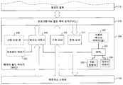
도 1은 본 발명의 여러 실시예들에 따른 메모리 시스템(100)의 블록도이다. 하나 이상의 실시예는 하나 이상의 발신(originating) 디바이스들(예를 들어, 하나 이상의 프로세서들)과 적층형 어레이 메모리 "볼트들"의 세트 사이에 지령들, 어드레스들, 및/또는 데이터의 복수의 아웃바운드 스트림(outbound stream)을 실질적으로 동시에 전송하도록 작동한다. 메모리 시스템 밀도, 대역폭, 병렬성(parallelism) 및 확장성이 증가될 수 있다.1 is a block diagram of a
본원에서 멀티-다이 메모리 어레이 실시예들은 이전 디자인들에서 각각의 개별 메모리 어레이 다이상에 정상적으로 배치되는 제어 로직을 종합하고 있다. 적층형 다이 그룹의 서브섹션들(이하 "메모리 볼트"로서 언급됨)은 공통의 제어 로직을 공유한다. 메모리 볼트 아키텍처는 파워드-온(powered-on) 메모리 뱅크들의 미세한 입상도(granularity)를 제공하면서 에너지 효율을 증가시키기 위해 메모리 제어 로직을 전략적으로 분할한다. 또한 본원에서 실시예들은 메모리 시스템 인터페이스에 대해 표준화된 호스트 프로세서를 사용할 수 있다. 표준화된 인터페이스는 메모리 기술이 발전함에 따라 재설계 사이클 시간을 감소시킬 수 있다.Multi-die memory array embodiments herein incorporate the control logic normally placed on each individual memory array die in previous designs. Subsections of the stacked die group (hereinafter referred to as "memory volts") share common control logic. The memory vault architecture strategically partitions the memory control logic to increase energy efficiency while providing fine granularity of powered-on memory banks. Embodiments herein may also use a host processor standardized for a memory system interface. Standardized interfaces can reduce redesign cycle times as memory technology advances.
도 2는 여러 실시예들에 따라 로직 다이(202)로 적층된 적층형-다이 3D 메모리 어레이(200)의 부분 개념 도면이다. 메모리 시스템(100)은 적층형-다이 3D 메모리 어레이(200)와 같은 타일형 메모리 어레이들의 스택을 하나 이상 통합하고 있다. 다중 메모리 어레이(예를 들어, 메모리 어레이(203))는 복수의 적층형 다이들(예를 들어, 적층형 다이(204)) 각각에 조립된다.2 is a partial conceptual diagram of a stacked-die
적층형 다이들 각각은 다중 "타일들"(예를 들어, 적층형 다이(204)와 관련된 타일들(205A, 205B, 205C))로 논리적으로 구분된다. 각각의 타일(예를 들어 타일(205C))은 하나 이상의 메모리 어레이(203)를 포함할 수 있다. 일부 실시예들에서, 각각의 메모리 어레이(203)는 메모리 시스템(100) 내에 하나 이상의 독립된 메모리 뱅크들로서 구성될 수 있다. 메모리 어레이(203)들은 어떠한 특별한 메모리 기술로 제한하지 않으며, DRAM(dynamic random access memory), SRAM(static random access memory), 플래시 메모리 등을 포함할 수 있다.Each of the stacked dies is logically divided into multiple “tiles” (eg,
메모리 어레이 타일(208)들의 적층형 세트는 적층형 다이들(예를 들어, 타일들(212B, 212C, 212D). 도 1에서 베이스 타일이 숨겨져 있음) 각각으로부터 단일 타일을 포함할 수 있다. 전력, 어드레스, 및/또는 데이터와, 이와 유사한 공통 신호들은 웨이퍼 관통 상호접속(TWI : through-wafer interconnect)과 같이, 전도성 경로들(예를 들어, 전도성 경로(224))상에 "Z" 크기(220)로서 타일(208)들의 적층형 세트를 횡단할 수 있다. 따라서 적층형-다이 3D 메모리 어레이(200)는 메모리 "볼트들"의 세트(예를 들어, 메모리 볼트(230))로 분할된다. 각각의 메모리 볼트는 타일들의 적층형 세트를 포함하고, 하나의 타일은 복수의 적층형 다이 각각으로부터 나온다. 볼트의 각각의 타일은 하나 이상의 메모리 어레이(예를 들어, 메모리 어레이(240))를 포함할 수 있다.The stacked set of
그 결과로 생성된 메모리 볼트들의 세트(102)가 도 1에 도시되어 있다. 이하에 설명된 제어, 스위칭 및 통신 로직은 로직 다이(202)상에 조립된다. 메모리 시스템(100)은 복수의 메모리 볼트 제어기(MVC)(104)(예를 들어, MVC(106))를 포함한다. 각각의 MVC는 대응하는 메모리 볼트(예를 들어, 메모리 볼트(110))에 1 대 1 관계로서 통신가능하게 연결된다. 따라서 각각의 MVC는 다른 MVC들과 그들 각자의 메모리 볼트들 사이의 통신으로부터 독립적으로 대응하는 메모리 볼트와 통신할 수 있다.The resulting set of
또한 메모리 시스템(100)은 복수의 구성가능한 직렬형 통신 링크 인터페이스(SCLI : serialized communication link interface)(112)를 포함한다. SCLI(112)들은 SCLI들의 아웃바운드 그룹(113)(예를 들어, 아웃바운드 SCLI(114)) 및 SCLI들의 인바운드(inbound) 그룹(115)으로 구분된다. 복수의 SCLI(112) 각각은 다른 SCLI(112)들과 동시 작동을 할 수 있다. SCLI(112)들은 다함께 복수의 MVC(104)들을 하나 이상의 호스트 프로세서(들)(114)에 통신가능하게 연결한다. 메모리 시스템(100)은 고도 추출된(highly abstracted) 멀티-링크 고처리율(high-throughput) 인터페이스를 호스트 프로세서(들)(114)에 제공한다.The
또한 메모리 시스템(100)은 매트릭스 스위치(116)를 포함할 수 있다. 매트릭스 스위치(116)는 복수의 SCLI(112) 및 복수의 MVC(104)에 통신가능하게 연결된다. 매트릭스 스위치(116)는 각각의 SCLI를 선택된 MVC에 교차접속할 수 있다. 호스트 프로세서(들)(114)는 따라서 실질적으로 동시에 복수의 SCLI(112)를 가로질러 복수의 메모리 볼트(102)에 접근할 수 있다. 이러한 아키텍처는 멀티-코어 기술들을 포함하는, 현대 프로세서 기술들에 의해 필요로 하는 프로세서 대 메모리 대역폭을 제공할 수 있다.The
또한 메모리 시스템(100)은 매트릭스 스위치(116)에 통신가능하게 연결된 메모리 패브릭(fabric) 제어 레지스터(117)를 포함할 수 있다. 메모리 패브릭 제어 레지스터(117)는 구성 소스로부터 메모리 패브릭 구성 파라미터들을 받아들이고, 그리고 선택가능한 모드에 따라 작동하도록 메모리 시스템(100)의 하나 이상의 컴포넌트를 구성한다. 예를 들어, 매트릭스 스위치(116), 각각의 복수의 메모리 볼트(102), 및 복수의 MVC(104)는 정상적으로는 별개의 메모리 요청들에 응답하여 서로 독립적으로 작동하도록 구성될 수 있다. 그러한 구성은 SCLI(112)들과 메모리 볼트(102)들 사이의 병렬성의 결과로서 메모리 시스템 대역폭을 강화시킬 수 있다.The
대안으로서, 메모리 시스템(100)은 복수의 메모리 볼트(102) 중 2개 이상의 메모리 볼트의 서브세트와 MVC들의 대응 서브세트가 단일 요청에 응답하여 동기 작동하도록 메모리 패브릭 제어 레지스터(117)를 경유하여 재구성될 수 있다. 후자의 구성은 아래에 더 상세히 설명되어 있듯이, 잠복기(latency)를 감소시키기 위해 정상보다 넓은(wider-than-normal) 데이터 워드에 접근하는데 사용될 수 있다. 다른 구성들은 선택된 비트 패턴을 메모리 패브릭 제어 레지스터(117)에 로딩시킴에 의하여 사용될 수 있다.Alternatively,
도 3 및 도 4는 여러 실시예들에 따라 각자의 예시적 패킷들(300 및 400)과 관련된 필드들을 도시하는 패킷 다이어그램들이다. 도 3 및 도 4를 고려하여 도 1로 돌아가면, 또한 메모리 시스템(100)은 매트릭스 스위치(116)에 통신가능하게 연결된 복수의 패킷 디코더(118)(예를 들어, 패킷 디코더(120))를 포함할 수 있다. 호스트 프로세서(들)(114)는 일부 실시예들에서 예시적 패킷(300 또는 400)과 구조가 유사한 아웃바운드 패킷(122)을 모은다. 즉, 아웃바운드 패킷(122)은 지령 필드(310), 어드레스 필드(320), 및/또는 데이터 필드(410)를 내장할 수 있다. 또한 아웃바운드 패킷(122)은 메모리 볼트 내의 프리페치 동작들과 관련된 프리페치 정보를 보유하기 위해 프리페치 정보 필드(412)를 내장할 수 있다. 프리페치 동작들은 도 5, 도 5a, 도 6a, 및 도 6b를 참고하여 아래에 설명되어 있다. 도 1로 돌아가서, 호스트 프로세서(114)가 아웃바운드 패킷(122)을 어셈블(assemble)한 후에, 호스트 프로세서는 이하에 상세히 설명된 방법으로 아웃바운드 패킷(122)을 아웃바운드 SCLI(예를 들어, 아웃바운드 SCLI(114))를 가로질러 패킷 디코더(120)로 전송한다.3 and 4 are packet diagrams showing fields associated with
아웃바운드 SCLI(114)는 복수의 아웃바운드 차동쌍 직렬 경로(differential pair serial path)(DPSP)(128)를 포함할 수 있다. DPSP(128)들은 호스트 프로세서(들)(114)에 통신가능하게 연결되고, 그리고 아웃바운드 패킷(122)을 집합적으로 운반할 수 있다. 즉, 복수의 DPSP(128) 중 각각의 DPSP는 제1 데이터 레이트에서 아웃바운드 패킷(122)의 제1 데이터 레이트 아웃바운드 서브-패킷 부분을 운반할 수 있다.
아웃바운드 SCLI(114)는 또한 복수의 아웃바운드 DPSP(128)에 통신가능하게 연결된 역직렬화기(130)를 포함할 수 있다. 역직렬화기(130)는 아웃바운드 패킷(122)의 각각의 제1 데이터 레이트 아웃바운드 서브-패킷 부분을 복수의 제2 데이터 레이트 아웃바운드 서브-패킷으로 변환한다. 복수의 제2 데이터 레이트 아웃바운드 서브-패킷은 제2 데이터 레이트에서 제1 복수의 아웃바운드 싱글-앤드(single-ended) 데이터 경로(SEDP)(134)를 가로질러 전송된다. 제2 데이터 레이트는 제1 데이터 레이트보다 더 느리다.The
아웃바운드 SCLI(114)는 또한 역직렬화기(130)에 통신가능하게 연결된 디멀티플렉서(demultiplexer)(138)를 포함할 수 있다. 디멀티플렉서(138)는 복수의 제2 데이터 레이트 아웃바운드 서브-패킷 각각을 복수의 제3 데이터 레이트 아웃바운드 서브-패킷으로 변환한다. 복수의 제3 데이터 레이트 아웃바운드 서브-패킷은 제2 복수의 아웃바운드 제3 데이터 레이트에서 SEDP(142)를 가로질러 패킷 디코더(120)로 전송된다. 제3 데이터 레이트는 제2 데이터 레이트보다 더 느리다.The
패킷 디코더(120)는 아웃바운드 패킷(122)을 수신하고, 지령 필드(310)(예를 들어, 예시적 패킷(300)), 어드레스 필드(320)(예를 들어, 예시적 패킷(300)), 및/또는 데이터 필드(예를 들어 예시적 패킷(400))를 추출한다. 일부 실시예들에서, 패킷 디코더(120)는 대응하는 메모리 볼트 선택 신호들의 세트를 결정하기 위해 어드레스 필드(320)를 디코딩한다. 패킷 디코더(120)는 인터페이스(146)상의 매트릭스 스위치(116)에 메모리 볼트 선택 신호들의 세트를 제공한다. 볼트 선택 신호들은 입력 데이터 경로(148)들이 아웃바운드 패킷(122)에 해당하는 MVC(106)로 전환되도록 만든다.The
이제 인바운드 데이터 경로들에 대해 설명하면, 메모리 시스템(100)은 매트릭스 스위치(116)에 통신가능하게 연결된 복수의 패킷 인코더(154)(예를 들어, 패킷 인코더(158))를 포함할 수 있다. 패킷 인코더(158)는 인바운드 메모리 지령, 인바운드 메모리 어드레스, 및/또는 인바운드 메모리 데이터를 복수의 MVC(104) 중 하나로부터 매트릭스 스위치(116)를 경유하여 수신할 수 있다. 패킷 인코더(158)는 인바운드 SCLI(164)를 가로질러 호스트 프로세서(114)로 전송하기 위해 인바운드 메모리 지령, 어드레스, 및/또는 데이터를 인바운드 패킷(160) 내로 인코딩한다.Referring now to inbound data paths,
일부 실시예들에서, 패킷 인코더(158)는 인바운드 패킷(160)을 복수의 제3 데이터 레이트 인바운드 서브-패킷으로 분할할 수 있다. 패킷 인코더(158)는 제3 데이터 레이트에서 복수의 제3 데이터 레이트 인바운드 서브-패킷을 제1 복수의 인바운드 싱글앤드 데이터 경로(SEDP)(166)를 가로질러 전송할 수 있다. 메모리 시스템(100)은 또한 패킷 인코더(158)에 통신가능하게 연결된 멀티플렉서(multiplexer)(168)를 포함할 수 있다. 멀티플렉서(168)는 제3 데이터 레이트 인바운드 서브-패킷들의 복수의 서브세트들 각각을 제2 데이터 레이트 인바운드 서브-패킷으로 멀티플렉싱할 수 있다. 멀티플렉서(168)는 제3 데이터 레이트보다 빠른 제2 데이터 레이트에서 제2 데이터 레이트 인바운드 서브-패킷들을 제2 복수의 인바운드 SEDP(170)를 가로질러 전송한다.In some embodiments,
메모리 시스템(100)은 멀티플렉서(168)에 통신가능하게 연결된 직렬화기(172)를 더 포함할 수 있다. 직렬화기(172)는 제2 데이터 레이트 인바운드 서브-패킷들의 복수의 서브세트들 각각을 제1 데이터 레이트 인바운드 서브-패킷 내로 집합시킨다. 제1 데이터 레이트 인바운드 서브-패킷들은 제2 데이트 레이트보다 빠른 제1 데이트 레이트에서 복수의 인바운드 차동쌍 직렬 경로(DPSP)(174)를 가로질러 호스트 프로세서(들)(114)로 전송된다. 따라서 지령, 어드레스 및 데이터 정보는 호스트 프로세서(들)(114)와 MVC(104)들 사이에서 매트릭스 스위치(116)를 경유하여 SCLI(112)들을 가로질러 전후로 전달된다.The
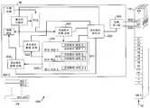
도 5는 여러 실시예들에 따른 MVC(예를 들어, MVC(106)) 및 관련 모듈들의 블록도이다. MVC(106)는 프로그램가능 볼트 제어 로직(PVCL) 컴포넌트(예를 들어, PVCL(510))을 포함할 수 있다. PVCL(510)은 MVC(106)를 대응하는 메모리 볼트(예를 들어, 메모리 볼트(110))에 인터페이스한다. PVCL(510)은 대응하는 메모리 볼트(110)와 관련된 하나 이상의 뱅크 제어 신호들 및/또는 타이밍 신호들을 발생한다.5 is a block diagram of an MVC (eg, MVC 106) and related modules in accordance with various embodiments.
PVCL(510)은 선택된 구성 또는 선택된 기술의 메모리 볼트(110)에 MVC(106)를 적응시키도록 구성될 수 있다. 따라서, 예를 들어 메모리 시스템(100)은 현재 이용가능한 DDR2 DRAM들을 이용하여 초기에 구성될 수 있다. 메모리 시스템(100)은 이어서 PVCL(510)이 DDR3 뱅크 제어 및 타이밍 로직을 포함하도록 재구성함으로써 DDR3-기반 메모리 볼트 기술을 수용하도록 적응될 수 있다.
MVC(106)는 또한 PVCL(510)에 통신가능하게 연결된 메모리 시퀀서(sequencer)(514)를 포함할 수 있다. 메모리 시퀀서(514)는 관련된 메모리 볼트(110)를 실행하는데 사용된 기술에 기초하여 메모리 기술에 의존한 동작들의 세트를 수행한다. 메모리 시퀀서(514)는 예를 들어, 지령 디코드 동작들, 메모리 어드레스 멀티플렉싱 동작들, 메모리 어드레스 디멀티플렉싱 동작들, 메모리 리프레시 동작들, 메모리 볼트 트레이닝 동작들, 및/또는 대응하는 메모리 볼트(110)와 관련된 메모리 볼트 프리페치 동작들을 수행할 수 있다. 일부 실시예들에서, 메모리 시퀀서(514)는 DRAM 시퀀서를 포함할 수 있다. 일부 실시예들에서, 메모리 리프레시 동작들은 리프레시 제어기(515)에서 시작될 수 있다.
메모리 시퀀서(514)는 선택된 구성 또는 기술의 메모리 볼트(110)에 메모리 시스템(100)을 적응시키도록 구성될 수 있다. 예를 들어, 메모리 시퀀서(514)는 메모리 시스템(100)과 관련된 다른 메모리 시퀀서들과 동기 작동되도록 구성될 수 있다. 그러한 구성은 멀티플 메모리 볼트들로부터의 넓은 데이터 워드를 단일 캐시 라인 요청에 응답하여 호스트 프로세서(들)(114)와 관련된 캐시 라인(도시 안됨)으로 전달하는데 사용될 수 있다.
또한 MVC(106)는 기록 버퍼(516)를 포함할 수 있다. 기록 버퍼(516)는 호스트 프로세서(들)(114)로부터 MVC(106)에 도달하는 데이터를 버퍼링하도록 PVCL(510)에 통신가능하게 연결될 수 있다. MVC(106)는 판독 버퍼(517)를 더 포함할 수 있다. 판독 버퍼(517)는 대응하는 메모리 볼트(110)로부터 MVC(106)에 도달하는 데이터를 버퍼링하도록 PVCL(510)에 통신가능하게 연결될 수 있다.
MVC(106)는 또한 고장(out-of-order) 요청 큐(518)를 포함할 수 있다. 고장 요청 큐(518)는 메모리 볼트(110) 내에 포함된 복수의 메모리 뱅크에서 판독 및/또는 기록 동작들의 명령에 따른 순서를 확립한다. 명령에 따른 순서는 뱅크 충돌을 감소시키며 판독-기록 전환 시간을 감소시키기 위해 어떤 단일 메모리 뱅크에서 순차적 동작들을 회피하도록 선택된다.
또한 MVC(106)는 메모리 볼트 리페어 로직(MVRL : memory vault repair logic) 컴포넌트(524)를 포함할 수 있다. MVRL(524)은 어레이 리페어 로직(526)을 이용하여 결함있는 메모리 어레이 어드레스 리맵핑(remapping) 동작들을 수행하도록 메모리 볼트(110)에 통신가능하게 연결될 수 있다. 또한 MVRL(524)은 TWI 리페어 로직(528)을 이용하여 메모리 볼트(110)와 관련된 TWI 리페어 동작들을 수행할 수 있다.
도 5a는 여러 실시예들에 따른 메모리 시스템(5000)의 블록도이다. 메모리 시스템(5000)은 메모리 볼트(102)들(예를 들어, 메모리 볼트(110))의 세트 및 대응하는 MVC(104)들(예를 들어 MVC(106))의 세트를 포함할 수 있다. MVC들은 전술한 바와 같이 메모리 어레이 다이들(예를 들어, 도 2의 메모리 어레이 다이(204))로 적층된 로직 다이(예를 들어, 도 2의 로직 다이(202))상에 조립된다.5A is a block diagram of a
도 5a의 아래 설명은 예시적 메모리 볼트(110), 예시적 MVC(106), 및 메모리 볼트 프리페치 동작들과 관련된 여러 구조 요소들 사이의 접속부들에 대해 언급하고 있다. 그러나, 주목해야 할 것은, 아래에 설명되고 도 5a에 예시된 접속부들 및 기능은 메모리 볼트(102)들의 세트 중 각각에 그리고 대응하는 MVC(104)들의 세트 각각에 적용된다는 점이다.The description below in FIG. 5A refers to connections between various structural elements associated with
메모리 시스템(5000)의 일부 실시예들에서, 메모리 볼트(102)의 대역폭은 메모리 요청들을 발신하는 디바이스(예를 들어, 호스트 컴퓨터)에 메모리 볼트(102)들을 연결하는 통신 채널들의 대역폭을 초과할 수 있다. 덧붙여, 발신 디바이스로부터의 요청 스트림은 연속적이 아닐 수 있다. 이러한 인자들은 메모리 볼트(102)들에서 초과 대역폭을 초래할 수 있다. 초과 대역폭은 프리페치 동작들을 수행하는데 사용될 수 있다. 프리페치 동작들은 메모리 볼트가 아이들(idle)일 때, 예를 들어 메모리 볼트에 대한 어떠한 판독 요청들도 메모리 볼트에서 처리되고 있지 않을 때 수행될 수 있다. 대안으로서, 프리페치 동작들은 메모리 볼트가 아이들이 아닐 때 수행될 수 있다.In some embodiments of the
메모리 시스템(5000)은 프리페치 제어기(5006)를 포함할 수 있다. 프리페치 제어기(5006)는 메모리 볼트(110)와 관련된 프리페치 동작들을 수행한다. 메모리 시스템(5000)은 또한 프리페치 캐시(5014) 내에 포함된 하나 이상의 프리페치 버퍼(5010)들을 포함할 수 있다. 프리페치 버퍼(5010)들은 프리페치 제어기(5006)에 통신가능하게 연결될 수 있다. 프리페치 버퍼(5010)들의 세트(예를 들어, 프리페치 버퍼(5018)들의 세트)는 판독 데이터의 하나 이상의 캐시 라인들(예를 들어, 캐시 라인(5020)들)을 저장하도록 그룹화될 수 있다. 프리페치 제어기(5006)는 캐시 라인(5020)들을 하나 이상 선택적으로 사용할 수 있도록 구성될 수 있다.The
프리페치 제어기(5006)는 메모리 볼트(110)를 향해 프리페치 판독 요청을 발행하도록 구성될 수 있어서, 프리페치 판독 요청은 메모리 볼트(110)가 아이들일 때 또는 메모리 볼트(110)가 아이들(idle)이 아닐 때 발행될 수 있다. 일부 실시예들에서, 프리페치 데이터 워드(들)는 이전 판독 요청에 응답하여 데이터 워드 판독에 해당하는 메모리 볼트 어드레스로부터 판독될 수 있다. 대안으로서 (또는 추가로), 프리페치 데이터 워드들은 MVC(106)를 향해 지령들을 발행하는 발신 디바이스에 의해 제공된 어드레스들의 범위로부터 선택된 메모리 볼트 어드레스로부터 판독될 수 있다. 예를 들어, 호스트 컴퓨터는 프리페치 버퍼(5010)들 내에 프리페칭되며 캐싱되도록 어드레스들의 범위를 특정할 수 있다.The
또한, 메모리 시스템(5000)은 프리페치 제어기(5006)에 통신가능하게 연결된 프리페치 기록 로직(5021)을 포함할 수 있다. 프리페치 기록 로직(5021)은 메모리 볼트(110) 및 프리페치 버퍼(5010)들을 추적하여 기록 데이터로 업데이트한다.The
메모리 시스템(5000)에 의한 프리페치의 사용은 다른 것들에 비하여 일부 동작 조건들하에서 더 필요로 할 수 있다. "집약성(locality)"은 전자 메모리 기술과 관련되어 있는 바와 같이, 다음 메모리 요청이 이전 요청과 동일한 메모리의 공간 영역으로부터 데이터를 참조할 것이라는 가능성을 말한다. 더 큰 집약성을 갖는 메모리 볼트 데이터 요청 스트림은 더 작은 집약성을 갖는 데이터 요청 스트림보다 프리페치 동작들로부터 더 많은 유익을 줄 수 있다. 그리고, 프리페치 동작들은 메모리 볼트(110)에서 전력을 소비한다는 점에 주목해야 한다. 결과적으로, 프리페치 제어기(5006)는 프리페치 동작들을 선택적으로 가능 및/또는 불가능하게 구성될 수 있다. 일부 실시예들은 데이터 스트림의 예상 집약성에 따라 및/또는 메모리 볼트(110)와 관련된 선택된 전력 비용을 목표로 하기 위해 프리페치 동작들을 가능/불가능하게 할 수 있다.The use of prefetch by
메모리 시스템(5000)은 프리페치 제어기(5006)에 통신가능하게 연결된 프리페치 활용 로직(5022)을 포함할 수 있다. 프리페치 활용 로직(5022)은 히트 측정 기간 동안에 캐시 라인 히트들의 개수를 추적한다. 본원의 내용에서의 "캐시 라인 히트(cache line hit)"는, 데이터 워드가 저장되어 있으며 상기 데이터 워드가 캐시 내에서 발견되는 메모리 볼트 어드레스를 판독 요청이 참조할 때 발생한다. 프리페치 제어기(5006)는 프리페치 캐시(5014)와 관련된 히트 레이트가 히트 레이트 측정 기간 동안에 선택된 임계값보다 작으면 프리페치 동작들을 불가능하도록 구성될 수 있다. 프리페치 동작들은 선택된 기간 동안 또는 프리페치 동작들을 재개하라는 지령이 호스트 컴퓨터와 같은 발신 디바이스로부터 수신될 때까지 불가능하게 될 수 있다. 일부 실시예들에서, 프리페치는 개별 캐시 라인에 기초하여 켜지거나 꺼질 수 있다.
메모리 시스템(5000)은 또한 메모리 볼트(110)에 배치된 하나 이상의 전압 센서(5026) 및/또는 온도 센서(5028)를 포함할 수 있다. 전력 모니터(5032)는 전압 센서(들)(5026) 및/또는 온도 센서(들)(5028)에 연결될 수 있다. 전력 모니터(5032)는 메모리 볼트(110)에서의 전력 소비 레벨를 프리페치 제어기(5006)에 지시할 수 있다. 프리페치 제어기(5006)는 메모리 볼트(110)에서의 전력 소비 레벨이 제1 선택 임계값보다 높으면 프리페치 동작들을 불가능하게 구성될 수 있다. 프리페치 동작들은 선택된 기간의 만료에 따라 다시 가능하게 될 수 있다. 대안으로서, 프리페치는 전력 소비 레벨이 제2 선택 임계값보다 낮거나, 또는 프리페치를 재개하도록 발신 디바이스로부터 지령을 수신하면, 다시 가능하게 될 수 있다.
메모리 시스템(5000)은 프리페치 제어기(5006)에 통신가능하게 연결된 프리페치 판독 로직(5036)을 더 포함할 수 있다. 프리페치 판독 로직(5036)은 MVC(106)에서 수신된 판독 요청이 하나 이상의 프리페치 워드를 참조하면 하나 이상의 프리페치 버퍼(5010)들로부터 하나 이상의 프리페치 워드들을 판독할 수 있다.
따라서, 메모리 시스템(100); 메모리 어레이들(200, 203, 240, 527); 다이(202, 204); 타일들(205A, 205B, 205C, 208, 212B, 212C, 212D); "Z" 크기(220); 경로들(224, 148); 메모리 볼트들(230, 102, 110); MVC들(104, 106); SCLI들(112, 113, 114, 115, 164); 프로세서(들)(114); 매트릭스 스위치(116); 레지스터(117); 패킷들(300, 400, 122, 160); 패킷 디코더들(118, 120); 필드들(310, 320, 410); DPSP들(128, 174); 역직렬화기(130); SEDP들(134, 142, 166, 170); 디멀티플렉서(138); 인터페이스(146); 패킷 인코더들(154, 158); 멀티플렉서(168); 직렬화기(172); PVCL(510); 메모리 시퀀서(514); 리프레시 제어기(515); 버퍼들(516, 517); 고장 요청 큐(518); MVRL(524); 어레이 리페어 로직(526); TWI 리페어 로직(528); 메모리 시스템(5000); 프리페치 제어기(5006); 프리페치 버퍼들(5010, 5018); 프리페치 캐시(5014); 캐시 라인들(5020); 프리페치 기록 로직(5021); 프리페치 활용 로직(5022); 센서들(5026, 5028); 전력 모니터(5032); 및 프리페치 판독 로직(5036) 모두는 본원에서 "모듈들"로서 특성을 가질 수 있다.Thus, the
모듈들은 메모리 시스템(5000)의 아키텍처에서 요구하는 대로 그리고 여러 실시예들의 특별한 실행에 적합한 대로, 하드웨어 회로망, 광학 컴포넌트들, 단일 또는 멀티-프로세서 회로들, 메모리 회로들, 컴퓨터-판독가능한 매체(그러나 소프웨어 목록이 아님) 내에 인코딩된 소프트웨어 프로그램 모듈들 및 객체들(objects), 펌웨어, 및 이들의 조합을 포함할 수 있다.Modules may include hardware circuitry, optical components, single or multi-processor circuits, memory circuits, computer-readable media, as required by the architecture of
여러 실시예들의 장치 및 시스템들은 고밀도 멀티-링크 고처리율 반도체 메모리 시스템(5000) 이외의 응용예들에서 유용하게 사용될 수 있다. 따라서, 본 발명의 여러 실시예들은 이것으로 제한하지 않는다. 메모리 시스템(5000)의 예시는 여러 실시예들의 구조를 일반적으로 이해시키기 위한 의도를 갖고 있다. 이것은 본원에서 설명된 구조들을 사용하였던 장치 및 시스템들의 요소들 및 특징들(features) 모두를 완전히 설명하는 것으로 사용될 의도는 없다.The apparatus and systems of various embodiments may be usefully used in applications other than the high density multi-link high throughput
여러 실시예들의 신규한 장치 및 시스템들은 컴퓨터들, 통신 및 신호 처리 회로, 단일-프로세서 또는 멀티-프로세서 모듈들, 단일 또는 멀티플 매립 프로세서들, 멀티-코어 프로세서들, 데이터 스위치들, 및 다중층 멀티칩 모듈들을 포함하는 주문형(application-specific) 모듈들을 포함하거나 통합될 수 있다. 그러한 장치 및 시스템들은 다양한 전자 시스템들, 즉 텔레비젼, 휴대폰, 개인용 컴퓨터(예를 들어, 랩탑 컴퓨터, 데스크탑 컴퓨터, 핸드헬드 컴퓨터, 태블릿 컴퓨터 등), 워크스테이션, 라디오, 비디오 플레이어, 오디오 플레이어(예를 들어, MP3(Motion Picture Experts Group, Audio Layer 3) 플레이어), 차량, 의료기구(예를 들어, 심장 모니터, 혈압 모니터 등), 셋탑 박스 등 내에 서브-컴포넌트로서 추가로 포함될 수 있다. 일부 실시예들은 다수의 방법을 포함할 수 있다.The novel apparatus and systems of the various embodiments include computers, communication and signal processing circuits, single-processor or multi-processor modules, single or multiple embedded processors, multi-core processors, data switches, and multilayer multi Application-specific modules including chip modules may be included or integrated. Such devices and systems include a variety of electronic systems, such as televisions, cell phones, personal computers (eg, laptop computers, desktop computers, handheld computers, tablet computers, etc.), workstations, radios, video players, audio players (eg For example, it may be further included as a sub-component in a Motion Picture Experts Group (MP3) player), a vehicle, a medical instrument (eg, a heart monitor, a blood pressure monitor, etc.), a set top box, or the like. Some embodiments may include a number of methods.
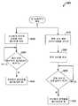
도 6a 및 도 6b는 여러 실시예들에 따른 방법(6000)을 예시하는 흐름도이다. 방법(6000)은 적층형-다이 메모리 시스템 내의 하나 이상의 메모리 볼트(예를 들어, 도 5a의 적층형-다이 메모리 시스템(5000) 내에 있는 메모리 볼트(110))와 관련된 프리페치 동작들을 수행하는 단계를 포함한다. 프리페치 동작들은 각각의 개별 메모리 볼트를 위해 개별적으로 구성된 프리페치 파라미터들을 선택적으로 사용가능 또는 불가능하게 될 수 있다. 일부 실시예들에서, 데이터 워드들의 프로그램가능 개수는 메모리 볼트 파이프라인이 비어 있을 때 때때로 프리페칭될 수 있다.6A and 6B are flowcharts illustrating a
방법(6000)은 발신 디바이스(예를 들어, 호스트 컴퓨터)로부터 MVC(도 5a의 MVC(106))에서 프리페치 구성 파라미터들을 수신하는 블록(6002)에서 시작할 수 있다. 프리페치 구성 파라미터들은 프리페치 어드레스 양상(modality)을 포함할 수 있다. 이 상황에서 "프리페치 어드레스 양상"은 메모리 볼트로부터 프리페칭될 어드레스가 이전에 액세스된 어드레스에 해당되는지 또는 발신 디바이스에 의해 특정된 범위로부터 나온 어드레스에 해당되는지를 의미한다. 다른 구성 파라미터들은 캐시 히트가 발생할 때 복귀하도록 캐시 라인들의 개수와 같은 캐시 라인 액세스 파라미터들을 포함할 수 있다. 또한 방법(6000)은 블록(6004)에서 프리페치 구성 파라미터들을 사용하여 메모리 시스템을 구성하는 단계를 포함할 수 있다.The
방법(6000)은 블록(6010)에서, 하나 이상의 프리페치 판독 요청을 메모리 볼트로 발행함으로써 계속될 수 있다. 방법(6000)은 메모리 볼트가 프리페치 판독 요청을 발행하기 전에 아이들인지를 확인할 수 있다. 메모리 볼트가 아이들이면, 예를 들어 메모리 볼트에 대해 어떠한 다른 판독 요청들도 메모리 볼트에서 처리되고 있지 않을 때, 방법(6000)은 프리페치 판독 요청을 발행할 수 있고 그리고 프리페치 동작들을 개시할 수 있다. 대안으로서, 방법(6000)은 메모리 볼트가 아이들이 아닐 때 프리페치 판독 요청을 발행할 수 있으며, 따라서 메모리 볼트에 대한 하나 이상의 다른 판독 요청들이 메모리 볼트에서 처리되고 있을지라도 프리페치 동작들이 판독 요청을 수신할 때 자동적으로 개시될 수 있다.The
방법(600)은 메모리 볼트가 프리페치 동작들을 수행하지 않도록 지시하는 프리페치 정보를 발신 디바이스(예를 들어, 호스트 컴퓨터)로부터 수신하면 메모리 볼트에 대해 프리페치 판독 요청을 발행하는 것(박스(6010))을 생략할 수 있다. 예를 들어, 방법(6000)이 도 1의 메모리 시스템(100)에서 사용될 때, 도 1의 호스트 프로세서(114)는 프리페치 동작들을 수행하지 않도록 지시하는 프리페치 정보를 갖는 아웃바운드 패킷(112)을 전송할 수 있다. 프리페치 정보는 도 4의 프리페치 정보 필드(412)와 같은 아웃바운드 패킷(122)의 필드 내에 포함될 수 있다. 메모리 볼트는 발신 디바이스로부터 프리페치 동작들이 수행되어야(또는 재개되어야) 할 것을 지시하는 프리페치 정보를 수신하면 프리페치 동작들을 수행하는 것을 재개할 수 있다. 프리페치 정보는 프리페치 동작들이 수행(또는 재개)되어야 하는지 아니면 수행되지 않아야(예를 들어 생략 또는 일시 중지) 하는지를 지시하는 값을 갖는 멀티플 비트들 또는 단지 단일 비트를 포함할 수 있다. 예를 들어, 프리페치 정보가 단지 단일 비트를 가지며 그리고 단일 비트가 "0"의 값을 가지면, 그때 프리페치 동작들은 생략되거나 일시 중지될 수 있다. 만일 단일 비트가 "1"의 값을 가지면, 그때 프리페치 동작이 수행(또는 재개)될 수 있다.The method 600 issues a prefetch read request for the memory vault upon receiving prefetch information from the originating device (eg, the host computer) instructing the memory vault not to perform prefetch operations (
도 6으로 돌아가서, 방법(6000)은 또한 블록(6014)에서 메모리 볼트에 해당하는 MVC에서 메모리 볼트로부터 하나 이상의 프리페치 데이터 워드를 수신하는 단계를 포함할 수 있다. 방법(6000)은 블록(6016)에서 프리페치 캐시에서 하나 이상의 프리페치 버퍼들 내에 프리페치 데이터 워드들을 저장하는 단계를 더 포함할 수 있다.Returning to FIG. 6, the
방법(6000)은 블록(6020)에서 MVC에서 판독 요청을 수신하는 것을 계속할 수 있다. 방법(6000)은 블록(6024)에서 판독 요청에 의해 참조한 데이터가 프리페치 캐시 내에 통용되고 있는지 판정하는 단계를 포함할 수 있다. '예' 이면, 방법(6000)은 블록(6028)에서 프리페치 캐시로부터 판독 요청을 서비스하며 그 결과 캐시 히트를 초래하는 것을 계속할 수 있다. 판독 요청에 의해 참조한 데이터가 프리페치 캐시 내에서 흐르지 않으면(캐시 히트가 없으면), 방법(6000)은 블록(6032)에서 선택된 메모리 볼트로부터 판독 요청을 서비스하는 것을 계속할 수 있다.The
또한 방법(6000)은 블록(6036)에서 제1 기간에 걸쳐 프리페치 캐시와 관련된 히트 레이트를 측정하는 단계를 포함할 수 있다. 방법(6000)은 추가로 블록(6040)에서 캐시 히트 레이트가 선택된 임계값보다 낮은지를 판정하는 단계를 포함할 수 있다. 히트 레이트가 선택된 임계값보다 낮으면, 방법(6000)은 블록(6044)에서 프리페치 동작들을 불가능하게 하는 단계를 포함할 수 있다. 프리페치 동작들은 선택된 기간 동안 또는 프리페치가 발신 디바이스로부터 수신된 지령을 경유하여 다시 가능하게 될 때까지 불가능하게 될 수 있다.The
일부 실시예들에서, 방법(6000)은 블록(6050)에서 선택된 메모리 볼트에서 전력 소비와 관련된 하나 이상의 동작 파라미터들을 모니터하는 단계를 포함할 수 있다. 예를 들어, 하나 이상의 전압 측정치들 및/또는 온도 측정치들은 메모리 볼트 내에 있는 센서들로부터 수신될 수 있다. 방법(6000)은 또한 블록(6054)에서 동작 파라미터들의 측정치들에 기초하여 메모리 볼트에서의 전력 소비를 계산하는 단계를 포함할 수 있다. 방법(6000)은 블록(6058)에서 전력 소비가 제1 선택 임계값보다 높은지를 판정하는 단계를 더 포함할 수 있다. 전력 소비가 제1 선택 임계값보다 높으면, 방법(6000)은 또한 블록(6062)에서 프리페치 동작들을 불가능하게 하는 단계를 포함할 수 있다. 프리페치 동작들은 선택된 기간 동안, 또는 전력 소비 레벨이 제2 선택 임계값보다 낮게 떨어질 때까지, 또는 프리페치가 발신 디바이스로부터 수신된 지령에 따라 다시 가능하게 될 때까지 불가능하게 될 수 있다.In some embodiments,
주목해야 할 것은, 본원에서 설명된 활동들은 설명된 순서 이외의 순서로 실행될 수 있다는 점이다. 상술한 방법들에 대하여 설명된 다양한 활동들은 또한 반복적, 직렬, 및/또는 병렬 방식으로 실행될 수 있다.It should be noted that the activities described herein may be executed in an order other than the described order. The various activities described with respect to the methods described above may also be executed in an iterative, serial, and / or parallel manner.
소프트웨어 프로그램은 소프트웨어 프로그램에 정의된 기능들을 실행하기 위해 컴퓨터-기반 시스템에서 컴퓨터-판독 가능한 프로그램으로부터 개시될 수 있다. 다양한 프로그래밍 언어들은 여기에 설명된 방법들을 실시하고 수행하도록 디자인된 소프트웨어 프로그램들을 만드는데 사용될 수 있다. 프로그램들은 Java 또는 C++와 같은 객체 지향 언어를 사용하여 객체지향 포맷으로 구성될 수 있다. 대안으로서, 프로그램들은 어셈블리 또는 C와 같은 절차 본위 언어를 사용하여 절차 본위 포맷으로 구성될 수 있다. 소프트웨어 컴포넌트들은 다른 것들 중에서 응용 프로그램 인터페이스, 인터-프로세스 통신 기술, 및 원격 절차 호출을 포함하는, 공지된 메카니즘들을 사용하여 통신할 수 있다. 여러 실시예들의 가르침은 어떠한 특별한 프로그래밍 언어 또는 환경으로 제한하지 않는다.The software program may be initiated from a computer-readable program in a computer-based system to perform the functions defined in the software program. Various programming languages can be used to create software programs designed to perform and perform the methods described herein. Programs can be organized in an object-oriented format using an object-oriented language such as Java or C ++. Alternatively, the programs can be organized in procedural format using an assembly or procedural language such as C. The software components can communicate using known mechanisms, including application program interfaces, inter-process communication techniques, and remote procedure calls, among others. The teachings of the various embodiments are not limited to any particular programming language or environment.
본원에서 설명된 장치, 시스템들, 및 방법들은 선택된 메모리 볼트와 관련된 파이프라인이 비어 있을 때 적층형-다이 메모리 시스템에서 선택된 메모리 볼트로부터 데이터 워드들의 프래그램가능 개수를 프리페치하도록 작동할 수 있다. 메모리 시스템 성능의 레벨이 증가될 수 있다.The apparatus, systems, and methods described herein may operate to prefetch a programmable number of data words from a selected memory vault in a stacked-die memory system when the pipeline associated with the selected memory vault is empty. The level of memory system performance may be increased.
예시에 따라 제한하지 않고, 첨부 도면들은 본 주제를 실시할 수 있는 특정 실시예들을 도시하고 있다. 예시된 실시예들은 기술에 숙련된 자가 여기에 설명된 가르침들을 실시할 수 있도록 충분히 상세하게 기술되어 있다. 다른 실시예들이 상기 실시예들로부터 유추되어 사용될 수 있으며, 따라서 구조적 및 논리적 대체 및 변경이 본원의 범위를 벗어나지 않고 가능하다. 따라서 "발명을 실시하기 위한 구체적인 내용"은 제한하는 의미로 받아들여서는 안 된다. 여러 실시예들의 폭은 첨부된 청구범위에서 형성되고 그러한 청구범위의 등가물의 전체 범위는 권리를 갖는다.Without limiting the example, the accompanying drawings illustrate specific embodiments in which the subject matter may be practiced. The illustrated embodiments are described in sufficient detail to enable those skilled in the art to practice the teachings described herein. Other embodiments may be inferred from the above embodiments, and thus structural and logical substitutions and changes are possible without departing from the scope of the present disclosure. Therefore, "details for carrying out the invention" should not be taken in a limiting sense. The breadth of the various embodiments is defined in the appended claims, and the full scope of equivalents of such claims is reserved.
본 발명의 주제의 그러한 실시예들은 용어 "발명"이 실제로 한번 이상 기술되어 있다면, 단순히 편리를 위해 그리고 본 출원을 어떠한 단일 발명 또는 발명의 개념으로 자발적으로 제한할 의도가 없이 개별적으로 또는 집합적으로 여기서 발명으로 언급될 수 있다. 따라서 특정 실시예들이 여기에 예시되고 설명되었지만, 동일한 목적을 달성하도록 계산된 어떠한 배열은 도시된 특정 실시예들로 대체될 수 있다. 상기 설명은 여러 실시예들의 모든 적용 또는 변화를 커버하도록 의도되어 있다. 상기 실시예들과 여기에 특별히 설명되지 않은 다른 실시예들의 조합은 상기 설명을 검토하여 기술에 숙련된 자들에게 명백히 나타날 것이다.Such embodiments of the subject matter of the present invention may be individually or collectively provided that the term “invention” is actually described more than once, simply for convenience and without the intention of spontaneously limiting the application to any single invention or concept of the invention. Reference may be made here to the invention. Thus, while specific embodiments have been illustrated and described herein, any arrangement calculated to achieve the same purpose may be replaced with the specific embodiments shown. The above description is intended to cover all adaptations or variations of various embodiments. Combinations of the above embodiments and other embodiments not specifically described herein will become apparent to those skilled in the art upon reviewing the above description.
본원의 요약은 독자가 기술적 설명의 성질을 신속히 알 수 있게 하는 요약을 요구하는 37 C.F.R. §1.72(b)에 부합하도록 제공되어 있다. 요약은 청구범위를 해석 또는 제한하는데 사용되지 않아야 함을 이해할 것이다. 상기 "발명을 실시하기 위한 구체적인 내용"에서, 여러 특징들은 본원을 간소화할 목적으로 단일 실시예로 함께 그룹으로 모인다. 본원의 방법은 각각의 청구항에서 명백히 언급한 것보다 더 많은 특징들을 요구하는 것으로 해석되어서는 안 된다. 오히려, 본 발명의 주제는 개시된 단일 실시예의 모든 특징들보다 더 작은 특징들에서 발견될 수 있다. 따라서 아래 청구범위는 각각의 청구항이 자체적으로 독립된 실시예를 가지면서 상기 "발명을 실시하기 위한 구체적인 내용"에 통합된다.The summary herein provides a summary that allows the reader to quickly understand the nature of the technical description. 37 C.F.R. It is provided to comply with §1.72 (b). It will be understood that the summary should not be used to interpret or limit the claims. In the foregoing description, various features are grouped together in a single embodiment for the purpose of streamlining the disclosure. The method herein should not be construed as requiring more features than are explicitly recited in each claim. Rather, the subject matter of the present invention can be found in features smaller than all the features of the disclosed single embodiment. Accordingly, the following claims are hereby incorporated into the above-mentioned "details for carrying out the invention" while each claim has its own independent embodiment.
Claims (39)
Translated fromKorean상기 적층형 메모리 다이들과 함께 적층된 로직 다이상에 배치되며, 상기 메모리 볼트와 관련된 제어, 스위칭 또는 통신 로직 중 적어도 하나를 제공하도록 상기 메모리 볼트에 통신가능하게 연결된 메모리 볼트 제어기(MVC : memory vault controller); 및
상기 메모리 볼트와 관련된 프리페치 동작들을 수행하기 위한 프리페치 제어기를 포함하는, 메모리 시스템.A memory vault including a plurality of stacked memory arrays each disposed in one of the plurality of stacked memory dies;
A memory vault controller disposed on a logic die stacked with the stacked memory dies and communicatively coupled to the memory vault to provide at least one of control, switching or communication logic associated with the memory vault. ); And
And a prefetch controller for performing prefetch operations associated with the memory vault.
판독 데이터의 적어도 하나의 캐시 라인을 저장하기 위해 상기 프리페치 제어기에 통신가능하게 연결된 프리페치 캐시에서의 적어도 하나의 프리페치 버퍼를 더 포함하는, 메모리 시스템.The method according to claim 1,
And at least one prefetch buffer in a prefetch cache communicatively coupled to the prefetch controller for storing at least one cache line of read data.
상기 프리페치 캐시는 복수의 프리페치 버퍼 세트를 포함하고, 각각의 프리페치 버퍼 세트는 캐시 라인을 포함하는, 메모리 시스템.The method according to claim 2,
Wherein the prefetch cache includes a plurality of prefetch buffer sets, each prefetch buffer set comprising a cache line.
상기 프리페치 제어기는 적어도 하나의 캐시 라인을 선택적으로 가능하도록 구성되는, 메모리 시스템.The method according to claim 3,
And the prefetch controller is configured to selectively enable at least one cache line.
상기 프리페치 제어기는 상기 메모리 볼트가 아이들(idle)일 때 상기 메모리 볼트에 대하여 프리페치 판독 요청을 발행하도록 구성되는, 메모리 시스템.The method according to claim 1,
The prefetch controller is configured to issue a prefetch read request for the memory vault when the memory vault is idle.
상기 프리페치 제어기는 이전 판독 요청에 응답하여 상기 메모리 볼트로부터 데이터 워드 판독에 해당하는 메모리 볼트 어드레스로부터 적어도 하나의 프리페치 데이터 워드를 판독하도록 구성되는, 메모리 시스템.The method according to claim 5,
The prefetch controller is configured to read at least one prefetch data word from a memory vault address corresponding to a data word read from the memory vault in response to a previous read request.
상기 프리페치 제어기는 상기 MVC에 지령들을 발행하는 발신 디바이스에 의해 제공된 어드레스들의 범위로부터 선택된 메모리 볼트 어드레스로부터 적어도 하나의 프리페치 데이터 워드를 판독하도록 구성되는, 메모리 시스템.The method according to claim 5,
The prefetch controller is configured to read at least one prefetch data word from a memory vault address selected from a range of addresses provided by an originating device issuing instructions to the MVC.
상기 프리페치 제어기는 프리페치 동작들을 선택적으로 가능하도록 구성되는, 메모리 시스템.The method according to claim 1,
And the prefetch controller is configured to selectively enable prefetch operations.
선택된 기간 동안에 다수의 캐시 라인 히트를 추적하도록 상기 프리페치 제어기에 통신가능하게 연결된 프리페치 활용 로직을 더 포함하는, 메모리 시스템.The method according to claim 1,
And prefetch utilization logic communicatively coupled to the prefetch controller to track a plurality of cache line hits for a selected period of time.
상기 프리페치 제어기는 프리페치 캐시와 관련된 히트 레이트가 제1 선택된 기간 동안 선택된 임계값보다 작으면 상기 프리페치 동작들을 사용할 수 없도록 구성되는, 메모리 시스템.The method according to claim 1,
And the prefetch controller is configured to disable the prefetch operations if the hit rate associated with the prefetch cache is less than the selected threshold for the first selected time period.
상기 프리페치 제어기는 제2 선택된 기간, 또는 상기 프리페치 동작들의 재개 지령이 발신 디바이스로부터 수신될 때까지 중에서 적어도 하나의 기간 동안에 상기 프리페치 동작들을 사용할 수 없도록 구성되는, 메모리 시스템.The method according to claim 10,
And the prefetch controller is configured to disable the prefetch operations for at least one of a second selected period, or until a resume instruction of the prefetch operations is received from an originating device.
상기 메모리 볼트 및 상기 프리페치 버퍼를 기록 데이터로 업데이트하기 위해 상기 프리페치 제어기에 통신가능하게 연결된 프리페치 기록 로직을 더 포함하는, 메모리 시스템.The method according to claim 1,
And prefetch write logic communicatively coupled to the prefetch controller to update the memory vault and the prefetch buffer with write data.
상기 MVC에서 수신한 판독 요청이 적어도 하나의 프리페치 워드를 참조한다면 적어도 하나의 프리페치 버퍼로부터 적어도 하나의 프리페치 워드를 판독하기 위해 상기 프리페치 제어기에 통신가능하게 연결된 프리페치 판독 로직을 더 포함하는, 메모리 시스템.The method according to claim 1,
And further comprising prefetch read logic communicatively coupled to the prefetch controller to read at least one prefetch word from at least one prefetch buffer if the read request received at the MVC references at least one prefetch word. Memory system.
상기 메모리 볼트에서의 전압 센서 또는 온도 센서 중 적어도 하나와;
상기 메모리 볼트에서 전력 소비 레벨을 상기 프리페치 제어기에 지시하기 위해 상기 전압 센서 또는 온도 센서에 연결된 전력 모니터를 더 포함하는, 메모리 시스템.The method according to claim 1,
At least one of a voltage sensor or a temperature sensor in the memory volt;
And a power monitor coupled to the voltage sensor or temperature sensor to instruct the prefetch controller a power consumption level in the memory volt.
상기 프리페치 제어기는 상기 메모리 볼트에서의 전력 소비 레벨이 제1 선택 임계값보다 큰 경우에 프리페치 동작들을 사용할 수 없게 구성되는, 메모리 시스템.The method according to claim 14,
The prefetch controller is configured to disable prefetch operations when the power consumption level in the memory volt is greater than a first selection threshold.
상기 프리페치 제어기는 선택된 주기, 제2 선택 임계값보다 낮게 떨어지는 전력 소비 레벨, 또는 상기 프리페치 동작들을 재개하도록 발신 디바이스로부터의 지령의 수신 중 적어도 하나를 따르는 상기 프리페치 동작들을 다시 가능하도록 구성되는, 메모리 시스템.The method according to claim 15,
The prefetch controller is configured to re-enable the prefetch operations following at least one of a selected period, a power consumption level falling below a second selection threshold, or receipt of a command from an originating device to resume the prefetch operations. , Memory system.
상기 프리페치 제어기는 상기 메모리 시스템내의 데이터 스트림의 집약성에 따라 상기 프리페치 동작들의 가능 및 불가능 중 적어도 하나를 수행하도록 구성되는, 메모리 시스템.The method according to claim 1,
And the prefetch controller is configured to perform at least one of enabling and disabling of the prefetch operations according to the density of data streams in the memory system.
상기 적층형 메모리 다이들과 함께 적층된 로직 다이상에 배치되며, 상기 메모리 볼트와 관련된 제어, 스위칭 또는 통신 로직 중 적어도 하나를 제공하도록 상기 메모리 볼트에 통신가능하게 연결된 메모리 볼트 제어기(MVC);
상기 메모리 볼트에 대하여 프리페치 판독 요청을 발행하기 위한 프리페치 제어기; 및
상기 프리페치 판독 요청과 관련된 적어도 하나의 프리페치 데이터 워드를 저장하기 위한 적어도 하나의 프리페치 버퍼를 포함하는, 메모리 시스템.A memory vault comprising a plurality of stacked memory arrays disposed respectively in one of the plurality of stacked memory dies;
A memory volt controller (MVC) disposed on a logic die stacked with the stacked memory dies and communicatively coupled to the memory volts to provide at least one of control, switching or communication logic associated with the memory volts;
A prefetch controller for issuing a prefetch read request for the memory vault; And
And at least one prefetch buffer for storing at least one prefetch data word associated with the prefetch read request.
선택된 기간 동안에 다수의 캐시 라인 히트를 추적하도록 상기 프리페치 제어기에 통신가능하게 연결된 프리페치 활용 로직을 더 포함하는, 메모리 시스템.The method according to claim 18,
And prefetch utilization logic communicatively coupled to the prefetch controller to track a plurality of cache line hits for a selected period of time.
상기 프리페치 제어기는 캐시 라인 히트들의 레이트가 선택된 레이트보다 클 때 프리페치 동작들을 수행하도록 구성되는, 메모리 시스템.The method according to claim 18,
And the prefetch controller is configured to perform prefetch operations when the rate of cache line hits is greater than the selected rate.
상기 프리페치 제어기는 상기 메모리 볼트가 아이들(idle)일 때 프리페치 동작들을 수행하도록 구성되는, 메모리 시스템.The method according to claim 18,
And the prefetch controller is configured to perform prefetch operations when the memory vault is idle.
상기 메모리 볼트의 선택된 전력 비용을 목표로 삼기 위해 상기 메모리 볼트와 관련된 프리페치 동작들의 가능 및 불가능 중 적어도 하나를 수행하도록 구성되는, 메모리 시스템.18. The method of claim 17,
And perform at least one of enabling and disabling of prefetch operations associated with the memory vault to target a selected power cost of the memory vault.
상기 선택된 메모리 볼트에 대해 프리페치 판독 요청을 발행하는 단계;
상기 선택된 메모리 볼트에 해당하는 메모리 볼트 제어기(MVC)에서 상기 선택된 메모리 볼트로부터 프리페치 데이터 워드를 수신하는 단계; 및
프리페치 캐시에 있는 프리페치 버퍼 내에 상기 프리페치 데이터 워드를 저장하는 단계를 더 포함하는 방법.The method according to claim 23,
Issuing a prefetch read request for the selected memory vault;
Receiving a prefetch data word from the selected memory vault at a memory vault controller (MVC) corresponding to the selected memory vault; And
Storing the prefetch data word in a prefetch buffer in a prefetch cache.
상기 프리페치 판독 요청은 상기 선택된 메모리 볼트에 대하여 어떠한 다른 판독 요청들도 상기 선택된 메모리 볼트에 의해 처리되고 있지 않을 때 발행되는 방법.The method of claim 24,
The prefetch read request is issued when no other read requests for the selected memory vault are being processed by the selected memory vault.
상기 MVC에서 판독 요청을 수신하는 단계;
이용가능한 경우에 상기 프리페치 캐시로부터 상기 판독 요청을 서비스하여 캐시 히트를 유발하는 단계; 및
캐시 히트가 없이 상기 선택된 메모리 볼트로부터 상기 판독 요청을 서비스하는 단계를 더 포함하는 방법.The method of claim 24,
Receiving a read request at the MVC;
Servicing the read request from the prefetch cache if available to cause a cache hit; And
Servicing the read request from the selected memory vault without a cache hit.
제1 기간에 걸쳐 상기 프리페치 캐시와 관련된 히트 레이트를 측정하는 단계;
상기 히트 레이트가 임계값 히트 레이트보다 작은지를 판정하는 단계; 및
상기 히트 레이트가 상기 임계값 히트 레이트보다 작으면 상기 프리페치 동작들을 불가능하게 하는 단계를 더 포함하는 방법.The method of claim 24,
Measuring a hit rate associated with the prefetch cache over a first period of time;
Determining if the hit rate is less than a threshold hit rate; And
Disabling the prefetch operations if the hit rate is less than the threshold hit rate.
상기 프리페치 동작들은 선택된 기간 또는 상기 프리페치 동작들을 재개하라는 지령이 발신 디바이스로부터 수신될 때까지 중에서 적어도 하나의 기간 동안에 불가능하게 되는 방법.The method of claim 27,
The prefetch operations are disabled for at least one of a selected period or until a command to resume the prefetch operations is received from an originating device.
상기 적층형-다이 메모리 시스템을 멀티-볼트 메모리 시스템으로서 구성하는 단계; 및
상기 프리페치 동작들을 각각의 메모리 볼트에서 독립적으로 수행하는 단계를 더 포함하는 방법.The method according to claim 23,
Configuring the stacked-die memory system as a multi-volt memory system; And
And independently performing the prefetch operations on each memory vault.
상기 선택된 메모리 볼트가 아이들(idle)인지를 확인하는 단계를 더 포함하는 방법.The method according to claim 23,
Determining whether the selected memory vault is idle.
상기 선택된 메모리 볼트에서 전력 소비와 관련된 적어도 하나의 동작 파라미터를 모니터하는 단계;
상기 적어도 하나의 동작 파라미터의 측정치에 기초하여 상기 선택된 메모리 볼트에서의 상기 전력 소비를 계산하는 단계;
상기 전력 소비가 제1 선택 임계값보다 높은지를 판정하는 단계; 및
상기 선택된 메모리 볼트에서의 상기 전력 소비가 상기 제1 선택 임계값보다 높으면 상기 프리페치 동작들을 불가능하게 하는 단계를 더 포함하는 방법.The method according to claim 23,
Monitoring at least one operating parameter associated with power consumption in the selected memory volt;
Calculating the power consumption at the selected memory volt based on the measurement of the at least one operating parameter;
Determining whether the power consumption is higher than a first selection threshold; And
Disabling the prefetch operations if the power consumption at the selected memory volt is higher than the first selection threshold.
상기 프리페치 동작들은 선택된 기간, 상기 전력 소비가 제2 선택 임계값보다 낮게 떨어질 때까지, 또는 상기 프리페치 동작들을 재개하라는 지령이 발신 디바이스로부터 수신될 때까지 중 적어도 하나의 기간 동안에 불가능하게 되는 방법.32. The method of claim 31,
Wherein the prefetch operations are disabled for at least one of a selected period, until the power consumption falls below a second selection threshold, or until a command to resume the prefetch operations is received from an originating device. .
상기 적어도 하나의 동작 파라미터를 모니터링하는 단계는 상기 메모리 볼트 내에 있는 센서들로부터 전압 레벨 측정치들 또는 온도 측정치들 중 적어도 하나를 수신하는 단계를 포함하는 방법.32. The method of claim 31,
Monitoring the at least one operating parameter comprises receiving at least one of voltage level measurements or temperature measurements from sensors in the memory volt.
상기 선택된 메모리 볼트에 대해 적어도 하나의 프리페치 판독 요청을 발행하는 단계;
각각의 프리페치 판독 요청을 위해, 상기 선택된 메모리 볼트에 해당하는 메모리 볼트 제어기(MVC)에서 상기 선택된 메모리 볼트로부터 프리페치 데이터 워드를 수신하는 단계;
프리페치 캐시에 있는 적어도 하나의 프리페치 버퍼 내에 상기 적어도 하나의 프리페치 데이터 워드를 저장하는 단계;
상기 MVC에서 적어도 하나의 판독 요청을 수신하는 단계;
이용가능한 경우에 상기 프리페치 캐시로부터 상기 적어도 하나의 판독 요청을 서비스하여 적어도 하나의 캐시 히트를 유발하는 단계; 및
상기 적어도 하나의 캐시 히트가 없이 상기 선택된 메모리 볼트로부터 상기 적어도 하나의 판독 요청을 서비스하는 단계를 더 포함하는 방법.35. The method of claim 34,
Issuing at least one prefetch read request for the selected memory vault;
Receiving a prefetch data word from the selected memory vault at a memory vault controller (MVC) corresponding to the selected memory vault for each prefetch read request;
Storing the at least one prefetch data word in at least one prefetch buffer in a prefetch cache;
Receiving at least one read request at the MVC;
Servicing the at least one read request from the prefetch cache if available to cause at least one cache hit; And
Servicing the at least one read request from the selected memory vault without the at least one cache hit.
발신 디바이스로부터 상기 MVC에서의 프리페치 구성 파라비터들을 수신하는 단계; 및
상기 프리페치 구성 파라미터들에 따라 상기 적층형-다이 메모리 시스템을 구성하는 단계를 더 포함하는 방법.36. The method of claim 35,
Receiving prefetch configuration parameters in the MVC from an originating device; And
Configuring the stacked-die memory system in accordance with the prefetch configuration parameters.
상기 프리페치 구성 파라미터들은 판독 데이터 요청에 응답하여 검색하기 위한 프리페치 어드레스 양상(modality) 또는 캐시 라인들의 개수 중 적어도 하나를 포함하는 방법.37. The method of claim 36,
Wherein the prefetch configuration parameters comprise at least one of a prefetch address modality or number of cache lines for retrieving in response to a read data request.
제1 기간에 걸쳐 상기 프리페치 캐시와 관련된 히트 레이트를 측정하는 단계;
상기 히트 레이트가 임계값 히트 레이트보다 작은지를 판정하는 단계; 및
상기 히트 레이트가 상기 임계값 히트 레이트보다 작으면 제2 기간 동안 상기 프리페치 동작들을 불가능하게 하는 단계를 더 포함하는 방법.36. The method of claim 35,
Measuring a hit rate associated with the prefetch cache over a first period of time;
Determining if the hit rate is less than a threshold hit rate; And
Disabling the prefetch operations for a second period if the hit rate is less than the threshold hit rate.
상기 선택된 메모리 볼트에서 전압 레벨 또는 온도 중 적어도 하나를 모니터하는 단계;
상기 전압 및/또는 온도의 측정치들에 기초하여 상기 선택된 메모리 볼트에서의 상기 전력 소비를 판정하는 단계;
상기 선택된 메모리 볼트에서의 상기 전력 소비가 제1 선택 임계값보다 높으면 상기 프리페치 동작들을 불가능하게 하는 단계; 및
상기 전력 소비가 제2 선택 임계값보다 낮으면 상기 프리페치 동작들을 다시 가능하게 하는 단계를 더 포함하는 방법.35. The method of claim 34,
Monitoring at least one of a voltage level or a temperature in the selected memory volt;
Determining the power consumption at the selected memory volt based on measurements of the voltage and / or temperature;
Disabling the prefetch operations if the power consumption at the selected memory volt is higher than a first selection threshold; And
Re-enabling the prefetch operations if the power consumption is lower than a second selection threshold.
Applications Claiming Priority (3)
| Application Number | Priority Date | Filing Date | Title |
|---|---|---|---|
| US12/371,389 | 2009-02-13 | ||
| US12/371,389US8364901B2 (en) | 2009-02-13 | 2009-02-13 | Memory prefetch systems and methods |
| PCT/US2010/024101WO2010093921A2 (en) | 2009-02-13 | 2010-02-12 | Memory prefetch systems and methods |
Related Child Applications (1)
| Application Number | Title | Priority Date | Filing Date |
|---|---|---|---|
| KR1020187015557ADivisionKR102030946B1 (en) | 2009-02-13 | 2010-02-12 | Memory prefetch systems and methods |
Publications (2)
| Publication Number | Publication Date |
|---|---|
| KR20110127193Atrue KR20110127193A (en) | 2011-11-24 |
| KR101865331B1 KR101865331B1 (en) | 2018-06-08 |
Family
ID=42560878
Family Applications (2)
| Application Number | Title | Priority Date | Filing Date |
|---|---|---|---|
| KR1020187015557AActiveKR102030946B1 (en) | 2009-02-13 | 2010-02-12 | Memory prefetch systems and methods |
| KR1020117020979AActiveKR101865331B1 (en) | 2009-02-13 | 2010-02-12 | Memory prefetch systems and methods |
Family Applications Before (1)
| Application Number | Title | Priority Date | Filing Date |
|---|---|---|---|
| KR1020187015557AActiveKR102030946B1 (en) | 2009-02-13 | 2010-02-12 | Memory prefetch systems and methods |
Country Status (7)
| Country | Link |
|---|---|
| US (3) | US8364901B2 (en) |
| EP (1) | EP2396790B1 (en) |
| JP (2) | JP2012518229A (en) |
| KR (2) | KR102030946B1 (en) |
| CN (1) | CN102349109B (en) |
| TW (1) | TWI494919B (en) |
| WO (1) | WO2010093921A2 (en) |
Cited By (3)
| Publication number | Priority date | Publication date | Assignee | Title |
|---|---|---|---|---|
| KR20160025613A (en)* | 2013-07-03 | 2016-03-08 | 마이크론 테크놀로지, 인크 | Memory controlled data movement and timing |
| US10157152B2 (en) | 2014-12-02 | 2018-12-18 | SK Hynix Inc. | Semiconductor device including a global buffer shared by a plurality of memory controllers |
| KR20190104642A (en)* | 2017-02-16 | 2019-09-10 | 마이크론 테크놀로지, 인크 | Active boundary quilting architecture memory |
Families Citing this family (29)
| Publication number | Priority date | Publication date | Assignee | Title |
|---|---|---|---|---|
| US7978721B2 (en) | 2008-07-02 | 2011-07-12 | Micron Technology Inc. | Multi-serial interface stacked-die memory architecture |
| US8364901B2 (en) | 2009-02-13 | 2013-01-29 | Micron Technology, Inc. | Memory prefetch systems and methods |
| US8018752B2 (en) | 2009-03-23 | 2011-09-13 | Micron Technology, Inc. | Configurable bandwidth memory devices and methods |
| US9123552B2 (en) | 2010-03-30 | 2015-09-01 | Micron Technology, Inc. | Apparatuses enabling concurrent communication between an interface die and a plurality of dice stacks, interleaved conductive paths in stacked devices, and methods for forming and operating the same |
| US8583894B2 (en)* | 2010-09-09 | 2013-11-12 | Advanced Micro Devices | Hybrid prefetch method and apparatus |
| GB2493191A (en)* | 2011-07-28 | 2013-01-30 | St Microelectronics Res & Dev | Cache arrangement with data pre-fetching requests having different quality of services |
| WO2013052056A1 (en)* | 2011-10-06 | 2013-04-11 | Intel Corporation | Apparatus and method for dynamically managing memory access bandwidth in multi-core processor |
| KR20140065678A (en)* | 2012-11-20 | 2014-05-30 | 에스케이하이닉스 주식회사 | Semiconductor apparatus and operating method for semiconductor apparatus using the same |
| US20140181415A1 (en)* | 2012-12-21 | 2014-06-26 | Advanced Micro Devices, Inc. | Prefetching functionality on a logic die stacked with memory |
| CN103915111B (en)* | 2013-01-09 | 2016-08-10 | 华邦电子股份有限公司 | Memory device and method for adjusting power supply thereof |
| US9183055B2 (en)* | 2013-02-07 | 2015-11-10 | Advanced Micro Devices, Inc. | Selecting a resource from a set of resources for performing an operation |
| US9679615B2 (en)* | 2013-03-15 | 2017-06-13 | Micron Technology, Inc. | Flexible memory system with a controller and a stack of memory |
| JP2016520226A (en)* | 2013-05-16 | 2016-07-11 | アドバンスト・マイクロ・ディバイシズ・インコーポレイテッドAdvanced Micro Devices Incorporated | Memory system with region specific memory access scheduling |
| US11768689B2 (en)* | 2013-08-08 | 2023-09-26 | Movidius Limited | Apparatus, systems, and methods for low power computational imaging |
| JP6287493B2 (en)* | 2014-03-31 | 2018-03-07 | 富士通株式会社 | Information processing apparatus, transfer apparatus, and control method |
| US10824335B2 (en)* | 2014-07-14 | 2020-11-03 | Western Digital Technologies, Inc. | Device and method to store predicted data at a host memory |
| US10114981B2 (en)* | 2016-12-31 | 2018-10-30 | Intel Corporation | Architecture for telemetry and adaptive lifetime control of integrated circuits |
| US10055384B2 (en)* | 2016-12-31 | 2018-08-21 | Entefy Inc. | Advanced zero-knowledge document processing and synchronization |
| US11442634B2 (en)* | 2018-04-12 | 2022-09-13 | Micron Technology, Inc. | Replay protected memory block command queue |
| US10831391B2 (en)* | 2018-04-27 | 2020-11-10 | EMC IP Holding Company LLC | Method to serve restores from remote high-latency tiers by reading available data from a local low-latency tier in a deduplication appliance |
| US10929062B2 (en)* | 2018-11-07 | 2021-02-23 | International Business Machines Corporation | Gradually throttling memory due to dynamic thermal conditions |
| KR102740370B1 (en)* | 2019-03-28 | 2024-12-06 | 에스케이하이닉스 주식회사 | Memory system, memory controller and operating method of thereof |
| EP4081889A4 (en)* | 2019-12-26 | 2023-05-31 | Micron Technology, Inc. | Host techniques for stacked memory systems |
| US11561731B2 (en) | 2019-12-26 | 2023-01-24 | Micron Technology, Inc. | Truth table extension for stacked memory systems |
| US11422934B2 (en) | 2020-07-14 | 2022-08-23 | Micron Technology, Inc. | Adaptive address tracking |
| US11409657B2 (en) | 2020-07-14 | 2022-08-09 | Micron Technology, Inc. | Adaptive address tracking |
| KR20220117747A (en) | 2021-02-17 | 2022-08-24 | 삼성전자주식회사 | Storage controller having data prefetching control function, operating method of storage controller, and operating method of storage device |
| US12164431B2 (en)* | 2021-11-30 | 2024-12-10 | Red Hat, Inc. | Managing prefetching operations for drives in distributed storage systems |
| KR20250058298A (en)* | 2023-10-23 | 2025-04-30 | 삼성전자주식회사 | Storage device based on flash memory and method for managing prefetch data thereof |
Citations (5)
| Publication number | Priority date | Publication date | Assignee | Title |
|---|---|---|---|---|
| KR100234647B1 (en)* | 1995-11-06 | 1999-12-15 | 포만 제프리 엘 | Data processing system with instruction prefetch |
| JP2004118305A (en)* | 2002-09-24 | 2004-04-15 | Sharp Corp | Cache memory controller |
| KR100449721B1 (en)* | 2002-05-20 | 2004-09-22 | 삼성전자주식회사 | Interface for devices having different data bus width and data transfer method using the same |
| JP2007537541A (en)* | 2004-05-14 | 2007-12-20 | マイクロン テクノロジー,インコーポレイテッド | Memory hub and method for memory sequencing |
| JP2008140220A (en)* | 2006-12-04 | 2008-06-19 | Nec Corp | Semiconductor device |
Family Cites Families (24)
| Publication number | Priority date | Publication date | Assignee | Title |
|---|---|---|---|---|
| JPS615357A (en)* | 1984-06-07 | 1986-01-11 | Fujitsu Ltd | Data processor |
| JP2631603B2 (en) | 1992-06-29 | 1997-07-16 | 川崎製鉄株式会社 | Metal strip winding device |
| JP3548616B2 (en)* | 1995-01-20 | 2004-07-28 | 株式会社日立製作所 | Information processing equipment |
| JPH1196081A (en)* | 1997-09-22 | 1999-04-09 | Chishiki Joho Kenkyusho:Kk | Storage device control method, storage device, and storage device manufacturing method |
| JP2001014840A (en) | 1999-06-24 | 2001-01-19 | Nec Corp | Plural line buffer type memory lsi |
| US6594730B1 (en)* | 1999-08-03 | 2003-07-15 | Intel Corporation | Prefetch system for memory controller |
| US7133972B2 (en)* | 2002-06-07 | 2006-11-07 | Micron Technology, Inc. | Memory hub with internal cache and/or memory access prediction |
| US6931494B2 (en)* | 2002-09-09 | 2005-08-16 | Broadcom Corporation | System and method for directional prefetching |
| US6983356B2 (en)* | 2002-12-19 | 2006-01-03 | Intel Corporation | High performance memory device-state aware chipset prefetcher |
| US7233880B2 (en)* | 2003-09-11 | 2007-06-19 | Intel Corporation | Adaptive cache algorithm for temperature sensitive memory |
| US7133324B2 (en)* | 2003-12-24 | 2006-11-07 | Samsung Electronics Co., Ltd. | Synchronous dynamic random access memory devices having dual data rate 1 (DDR1) and DDR2 modes of operation and methods of operating same |
| JP4444770B2 (en)* | 2004-09-14 | 2010-03-31 | シャープ株式会社 | Memory device |
| US20070005902A1 (en)* | 2004-12-07 | 2007-01-04 | Ocz Technology Group, Inc. | Integrated sram cache for a memory module and method therefor |
| US7327600B2 (en)* | 2004-12-23 | 2008-02-05 | Unity Semiconductor Corporation | Storage controller for multiple configurations of vertical memory |
| US20080126690A1 (en)* | 2006-02-09 | 2008-05-29 | Rajan Suresh N | Memory module with memory stack |
| US7283418B2 (en)* | 2005-07-26 | 2007-10-16 | Micron Technology, Inc. | Memory device and method having multiple address, data and command buses |
| JP4600825B2 (en)* | 2005-09-16 | 2010-12-22 | エルピーダメモリ株式会社 | Semiconductor memory device |
| WO2007095080A2 (en)* | 2006-02-09 | 2007-08-23 | Metaram, Inc. | Memory circuit system and method |
| US20070204106A1 (en)* | 2006-02-24 | 2007-08-30 | James Donald | Adjusting leakage power of caches |
| US20070220207A1 (en)* | 2006-03-14 | 2007-09-20 | Bryan Black | Transferring data from stacked memory |
| US8032711B2 (en)* | 2006-12-22 | 2011-10-04 | Intel Corporation | Prefetching from dynamic random access memory to a static random access memory |
| US7917702B2 (en)* | 2007-07-10 | 2011-03-29 | Qualcomm Incorporated | Data prefetch throttle |
| US20100121994A1 (en)* | 2008-11-10 | 2010-05-13 | International Business Machines Corporation | Stacked memory array |
| US8364901B2 (en) | 2009-02-13 | 2013-01-29 | Micron Technology, Inc. | Memory prefetch systems and methods |
- 2009
- 2009-02-13USUS12/371,389patent/US8364901B2/enactiveActive
- 2010
- 2010-02-12KRKR1020187015557Apatent/KR102030946B1/enactiveActive
- 2010-02-12EPEP10741802.2Apatent/EP2396790B1/enactiveActive
- 2010-02-12WOPCT/US2010/024101patent/WO2010093921A2/enactiveApplication Filing
- 2010-02-12CNCN201080012003.7Apatent/CN102349109B/enactiveActive
- 2010-02-12KRKR1020117020979Apatent/KR101865331B1/enactiveActive
- 2010-02-12JPJP2011550273Apatent/JP2012518229A/enactivePending
- 2010-02-12TWTW099104871Apatent/TWI494919B/enactive
- 2013
- 2013-01-28USUS13/751,502patent/US8607002B2/enactiveActive
- 2013-12-09USUS14/100,921patent/US8990508B2/enactiveActive
- 2014
- 2014-12-04JPJP2014245766Apatent/JP6127038B2/enactiveActive
Patent Citations (5)
| Publication number | Priority date | Publication date | Assignee | Title |
|---|---|---|---|---|
| KR100234647B1 (en)* | 1995-11-06 | 1999-12-15 | 포만 제프리 엘 | Data processing system with instruction prefetch |
| KR100449721B1 (en)* | 2002-05-20 | 2004-09-22 | 삼성전자주식회사 | Interface for devices having different data bus width and data transfer method using the same |
| JP2004118305A (en)* | 2002-09-24 | 2004-04-15 | Sharp Corp | Cache memory controller |
| JP2007537541A (en)* | 2004-05-14 | 2007-12-20 | マイクロン テクノロジー,インコーポレイテッド | Memory hub and method for memory sequencing |
| JP2008140220A (en)* | 2006-12-04 | 2008-06-19 | Nec Corp | Semiconductor device |
Cited By (6)
| Publication number | Priority date | Publication date | Assignee | Title |
|---|---|---|---|---|
| KR20160025613A (en)* | 2013-07-03 | 2016-03-08 | 마이크론 테크놀로지, 인크 | Memory controlled data movement and timing |
| KR20190107178A (en)* | 2013-07-03 | 2019-09-18 | 마이크론 테크놀로지, 인크 | Memory controlled data movement and timing |
| US11074169B2 (en) | 2013-07-03 | 2021-07-27 | Micron Technology, Inc. | Programmed memory controlled data movement and timing within a main memory device |
| US10157152B2 (en) | 2014-12-02 | 2018-12-18 | SK Hynix Inc. | Semiconductor device including a global buffer shared by a plurality of memory controllers |
| KR20190104642A (en)* | 2017-02-16 | 2019-09-10 | 마이크론 테크놀로지, 인크 | Active boundary quilting architecture memory |
| US11355162B2 (en) | 2017-02-16 | 2022-06-07 | Micron Technology, Inc. | Active boundary quilt architecture memory |
Also Published As
| Publication number | Publication date |
|---|---|
| EP2396790A2 (en) | 2011-12-21 |
| US20140156946A1 (en) | 2014-06-05 |
| TW201037704A (en) | 2010-10-16 |
| JP2012518229A (en) | 2012-08-09 |
| CN102349109A (en) | 2012-02-08 |
| US8607002B2 (en) | 2013-12-10 |
| CN102349109B (en) | 2015-08-26 |
| KR101865331B1 (en) | 2018-06-08 |
| TWI494919B (en) | 2015-08-01 |
| EP2396790A4 (en) | 2013-10-30 |
| US20100211745A1 (en) | 2010-08-19 |
| US20130145098A1 (en) | 2013-06-06 |
| WO2010093921A3 (en) | 2010-10-28 |
| JP6127038B2 (en) | 2017-05-10 |
| EP2396790B1 (en) | 2017-08-23 |
| WO2010093921A2 (en) | 2010-08-19 |
| KR20180063372A (en) | 2018-06-11 |
| US8990508B2 (en) | 2015-03-24 |
| JP2015079524A (en) | 2015-04-23 |
| US8364901B2 (en) | 2013-01-29 |
| KR102030946B1 (en) | 2019-10-10 |
Similar Documents
| Publication | Publication Date | Title |
|---|---|---|
| KR102030946B1 (en) | Memory prefetch systems and methods | |
| US8806131B2 (en) | Multi-serial interface stacked-die memory architecture | |
| US10297340B2 (en) | Switched interface stacked-die memory architecture |
Legal Events
| Date | Code | Title | Description |
|---|---|---|---|
| PA0105 | International application | Patent event date:20110908 Patent event code:PA01051R01D Comment text:International Patent Application | |
| PG1501 | Laying open of application | ||
| A201 | Request for examination | ||
| PA0201 | Request for examination | Patent event code:PA02012R01D Patent event date:20150212 Comment text:Request for Examination of Application | |
| E902 | Notification of reason for refusal | ||
| PE0902 | Notice of grounds for rejection | Comment text:Notification of reason for refusal Patent event date:20161013 Patent event code:PE09021S01D | |
| E90F | Notification of reason for final refusal | ||
| PE0902 | Notice of grounds for rejection | Comment text:Final Notice of Reason for Refusal Patent event date:20170821 Patent event code:PE09021S02D | |
| E701 | Decision to grant or registration of patent right | ||
| PE0701 | Decision of registration | Patent event code:PE07011S01D Comment text:Decision to Grant Registration Patent event date:20180227 | |
| PA0104 | Divisional application for international application | Comment text:Divisional Application for International Patent Patent event code:PA01041R01D Patent event date:20180531 | |
| PR0701 | Registration of establishment | Comment text:Registration of Establishment Patent event date:20180531 Patent event code:PR07011E01D | |
| PR1002 | Payment of registration fee | Payment date:20180601 End annual number:3 Start annual number:1 | |
| PG1601 | Publication of registration | ||
| PR1001 | Payment of annual fee | Payment date:20210524 Start annual number:4 End annual number:4 | |
| PR1001 | Payment of annual fee | Payment date:20220520 Start annual number:5 End annual number:5 | |
| PR1001 | Payment of annual fee | Payment date:20230522 Start annual number:6 End annual number:6 | |
| PR1001 | Payment of annual fee | Payment date:20240521 Start annual number:7 End annual number:7 |