KR20110112992A - Organic light emitting device and method for manufacturing same - Google Patents
Organic light emitting device and method for manufacturing sameDownload PDFInfo
- Publication number
- KR20110112992A KR20110112992AKR20100032286AKR20100032286AKR20110112992AKR 20110112992 AKR20110112992 AKR 20110112992AKR 20100032286 AKR20100032286 AKR 20100032286AKR 20100032286 AKR20100032286 AKR 20100032286AKR 20110112992 AKR20110112992 AKR 20110112992A
- Authority
- KR
- South Korea
- Prior art keywords
- layer
- oxide
- sulfide
- nitrides
- light emitting
- Prior art date
- Legal status (The legal status is an assumption and is not a legal conclusion. Google has not performed a legal analysis and makes no representation as to the accuracy of the status listed.)
- Ceased
Links
Images

Classifications
- H—ELECTRICITY
- H10—SEMICONDUCTOR DEVICES; ELECTRIC SOLID-STATE DEVICES NOT OTHERWISE PROVIDED FOR
- H10K—ORGANIC ELECTRIC SOLID-STATE DEVICES
- H10K50/00—Organic light-emitting devices
- H10K50/80—Constructional details
- H10K50/805—Electrodes
- H10K50/82—Cathodes
- H10K50/826—Multilayers, e.g. opaque multilayers
- H—ELECTRICITY
- H10—SEMICONDUCTOR DEVICES; ELECTRIC SOLID-STATE DEVICES NOT OTHERWISE PROVIDED FOR
- H10K—ORGANIC ELECTRIC SOLID-STATE DEVICES
- H10K50/00—Organic light-emitting devices
- H10K50/10—OLEDs or polymer light-emitting diodes [PLED]
- H10K50/17—Carrier injection layers
- H—ELECTRICITY
- H10—SEMICONDUCTOR DEVICES; ELECTRIC SOLID-STATE DEVICES NOT OTHERWISE PROVIDED FOR
- H10K—ORGANIC ELECTRIC SOLID-STATE DEVICES
- H10K59/00—Integrated devices, or assemblies of multiple devices, comprising at least one organic light-emitting element covered by group H10K50/00
- H10K59/10—OLED displays
- H10K59/12—Active-matrix OLED [AMOLED] displays
- H10K59/123—Connection of the pixel electrodes to the thin film transistors [TFT]
Landscapes
- Physics & Mathematics (AREA)
- Optics & Photonics (AREA)
- Electroluminescent Light Sources (AREA)
- Thin Film Transistor (AREA)
Abstract
Translated fromKoreanDescription
Translated fromKorean유기 발광 장치 및 이의 제조 방법에 관한 것이다.An organic light emitting device and a method of manufacturing the same.
유기 발광 장치(organic light emitting device)는 자발광형 장치로서 시야각이 넓고 콘트라스트가 우수할 뿐만 아니라, 응답시간이 빠르며, 휘도, 구동전압 및 응답속도 특성이 우수하고 다색화가 가능하다는 장점을 가지고 있다.The organic light emitting device is a self-luminous device, which has a wide viewing angle, excellent contrast, fast response time, excellent luminance, driving voltage and response speed, and multiple colors.
일반적인 유기 발광 장치는 애노드 및 캐소드와 상기 애노드 및 캐소드 사이에 개재된 유기층을 포함할 수 있다. 상기 유기층은, 정공수송층, 발광층, 전자수송층 및 캐소드 등을 포함할 수 있다. 또한, 상기 유기 발광 장치는 구동 트랜지스터 또는 스위칭 트랜지터 등을 포함할 수 있다.A general organic light emitting device may include an anode and a cathode and an organic layer interposed between the anode and the cathode. The organic layer may include a hole transport layer, a light emitting layer, an electron transport layer and a cathode. In addition, the organic light emitting device may include a driving transistor or a switching transistor.
상술한 바와 같은 구조를 갖는 유기 발광 장치의 구동 원리는 다음과 같다.The driving principle of the organic light emitting device having the structure as described above is as follows.
상기 애노드 및 캐소드 간에 전압을 인가하면, 애노드로부터 주입된 정공은 정공수송층을 경유하여 발광층으로 이동하고, 캐소드로부터 주입된 전자는 전자수송층을 경유하여 발광층으로 이동한다. 상기 정공 및 전자와 같은 캐리어들은 발광층 영역에서 재결합하여 엑시톤(exiton)을 생성하는데, 이 엑시톤이 여기 상태에서 기저상태로 변하면서 광이 생성된다.When a voltage is applied between the anode and the cathode, holes injected from the anode move to the light emitting layer via the hole transport layer, and electrons injected from the cathode move to the light emitting layer via the electron transport layer. Carriers such as holes and electrons recombine in the emission layer to generate excitons, which generate light as the excitons change from excited to ground state.
한편, 대면적 유기 발광 장치를 구현하기 위하여, 유기층을 습식 공정(wet process)을 이용하여 형성하고자 하는 연구가 최근 진행되고 있다.On the other hand, in order to implement a large area organic light emitting device, a study for forming an organic layer using a wet process has been recently conducted.
공정 안정성을 제공할 수 있으면서도 우수한 전기적 특성을 갖는 유기 발광 장치를 제공하는 것이다.It is to provide an organic light emitting device capable of providing process stability and having excellent electrical properties.
공정 안정성을 제공할 수 있는 유기 발광 장치의 제조 방법을 제공하는 것이다.It is to provide a method for manufacturing an organic light emitting device that can provide process stability.
기판;Board;
상기 기판 상에 형성되며, 소스 전극 및 드레인 전극, 산화물 반도체층, 게이트 전극, 및 상기 게이트 전극을 상기 소스 전극 및 드레인 전극과 절연시키는 게이트 절연층을 포함한 박막 트랜지스터;A thin film transistor formed on the substrate, the thin film transistor including a source electrode and a drain electrode, an oxide semiconductor layer, a gate electrode, and a gate insulating layer insulating the gate electrode from the source electrode and the drain electrode;
상기 박막 트랜지스터 상에 형성된 제1절연층;A first insulating layer formed on the thin film transistor;
상기 제1절연층 상에 형성되며 상기 박막 트랜지스터의 소스 전극 및 드레인 전극 중 하나와 연결된 캐소드;A cathode formed on the first insulating layer and connected to one of a source electrode and a drain electrode of the thin film transistor;
상기 캐소드 상에 형성되며, 금속, 금속 황화물, 금속 산화물, 금속 질화물, 및 이들 중 2 이상의 조합으로 이루어진 군으로부터 선택된 제1물질을 포함한 제1층;A first layer formed on the cathode and comprising a first material selected from the group consisting of metals, metal sulfides, metal oxides, metal nitrides, and combinations of two or more thereof;
상기 제1층 상에 형성된 유기층; 및An organic layer formed on the first layer; And
상기 유기층 상에 형성된 애노드;An anode formed on the organic layer;
를 포함한 유기 발광 장치가 제공된다.An organic light emitting device is provided.
상기 산화물 반도체층은 아연-함유 산화물을 포함할 수 있다.The oxide semiconductor layer may include a zinc-containing oxide.
상기 아연-함유 산화물은 제1성분을 더 포함하고, 상기 제1성분은 Hf, Y, Ta, Zr, Ga, Al, In, Fe, Sc, Lu, Yb, Tm, Er, Ho, Y, Mn, Co, Ni, Ti, Ge, Cu, Mo, Sn, 및 이들 중 2 이상의 조합으로 이루어진 군으로부터 선택될 수 있다.The zinc-containing oxide further includes a first component, wherein the first component is Hf, Y, Ta, Zr, Ga, Al, In, Fe, Sc, Lu, Yb, Tm, Er, Ho, Y, Mn , Co, Ni, Ti, Ge, Cu, Mo, Sn, and combinations of two or more thereof.
상기 캐소드는 Mg, Al, Ca, In, Ag, 및 이들 중 2 이상의 조합으로 이루어진 군으로부터 선택된 물질을 포함할 수 있다.The cathode may include a material selected from the group consisting of Mg, Al, Ca, In, Ag, and combinations of two or more thereof.
상기 제1물질은 2.6 eV 내지 4.6 eV 범위의 일함수를 가질 수 있다.The first material may have a work function in the range of 2.6 eV to 4.6 eV.
상기 제1물질은, K, Rb, Cs, Mg, Sr, Ba, Sc, Y, Ti, Mn, Zn, Yb, K 황화물, Rb 황화물, Cs 황화물, Mg 황화물, Sr 황화물, Ba 황화물, Sc 황화물, Y 황화물, Ti 황화물, Mn 황화물, Zn 황화물, Yb 황화물, K 산화물, Rb 산화물, Cs 산화물, Mg 산화물, Sr 산화물, Ba 산화물, Sc 산화물, Y 산화물, Ti 산화물, Mn 산화물, Zn 산화물, Yb 산화물, K 질화물, Rb 질화물, Cs 질화물, Mg 질화물, Sr 질화물, Ba 질화물, Sc 질화물, Y 질화물, Ti 질화물, Mn 질화물, Zn 질화물, Yb 질화물, 및 이들 중 2 이상의 조합으로 이루어진 군으로부터 선택될 수 있다.The first material is K, Rb, Cs, Mg, Sr, Ba, Sc, Y, Ti, Mn, Zn, Yb, K sulfide, Rb sulfide, Cs sulfide, Mg sulfide, Sr sulfide, Ba sulfide, Sc sulfide , Y sulfide, Ti sulfide, Mn sulfide, Zn sulfide, Yb sulfide, K oxide, Rb oxide, Cs oxide, Mg oxide, Sr oxide, Ba oxide, Sc oxide, Y oxide, Ti oxide, Mn oxide, Zn oxide, Yb Oxide, K nitride, Rb nitride, Cs nitride, Mg nitride, Sr nitride, Ba nitride, Sc nitride, Y nitride, Ti nitride, Mn nitride, Zn nitride, Yb nitride, and combinations of two or more thereof Can be.
상기 제1층은 전자 주입 물질을 더 포함할 수 있다.The first layer may further include an electron injection material.
상기 제1층의 두께는 3 nm 내지 30 nm일 수 있다.The thickness of the first layer may be 3 nm to 30 nm.
상기 제1층과 상기 캐소드 사이에는 전자 주입층이 개재될 수 있다.An electron injection layer may be interposed between the first layer and the cathode.
한편, 기판 상에, 소스 전극 및 드레인 전극, 산화물 반도체층, 게이트 전극, 및 상기 게이트 전극을 상기 소스 전극 및 드레인 전극과 절연시키는 게이트 절연층을 포함한 박막 트랜지스터를 형성하는 단계;On the other hand, forming a thin film transistor including a source electrode and a drain electrode, an oxide semiconductor layer, a gate electrode, and a gate insulating layer that insulates the gate electrode from the source electrode and the drain electrode;
상기 박막 트랜지스터 상에 제1절연층을 형성하는 단계;Forming a first insulating layer on the thin film transistor;
상기 제1절연층 상에 박막 트랜지스터의 소스 전극 및 드레인 전극 중 하나와 연결된 캐소드를 형성하는 단계;Forming a cathode connected to one of a source electrode and a drain electrode of the thin film transistor on the first insulating layer;
증착법 또는 스퍼터링법을 이용하여 상기 캐소드 상에 금속, 금속 황화물, 금속 산화물, 금속 질화물, 및 이들 중 2 이상의 조합으로 이루어진 군으로부터 선택된 제1물질을 포함한 제1층을 형성하는 단계;Forming a first layer comprising a first material selected from the group consisting of metals, metal sulfides, metal oxides, metal nitrides, and combinations of two or more thereof on the cathode using deposition or sputtering;
상기 제1층 상에 유기층을 형성하는 단계; 및Forming an organic layer on the first layer; And
상기 유기층 상에 애노드를 형성하는 단계;Forming an anode on the organic layer;
를 포함하는 유기 발광 장치의 제조 방법이 제공된다.A method of manufacturing an organic light emitting device is provided.
상기 산화물 반도체층은 제1성분을 더 포함하고, 상기 제1성분은 Hf, Y, Ta, Zr, Ga, Al, In, Fe, Sc, Lu, Yb, Tm, Er, Ho, Y, Mn, Co, Ni, Ti, Ge, Cu, Mo, 및 이들 중 2 이상의 조합으로 이루어진 군으로부터 선택될 수 있다.The oxide semiconductor layer further includes a first component, wherein the first component is Hf, Y, Ta, Zr, Ga, Al, In, Fe, Sc, Lu, Yb, Tm, Er, Ho, Y, Mn, Co, Ni, Ti, Ge, Cu, Mo, and combinations of two or more thereof.
상기 제1물질은 2.6 eV 내지 4.6 eV 범위의 일함수를 가질 수 있다.The first material may have a work function in the range of 2.6 eV to 4.6 eV.
상기 제1물질은, K, Rb, Cs, Mg, Sr, Ba, Sc, Y, Ti, Mn, Zn, Yb, K 황화물, Rb 황화물, Cs 황화물, Mg 황화물, Sr 황화물, Ba 황화물, Sc 황화물, Y 황화물, Ti 황화물, Mn 황화물, Zn 황화물, Yb 황화물, K 산화물, Rb 산화물, Cs 산화물, Mg 산화물, Sr 산화물, Ba 산화물, Sc 산화물, Y 산화물, Ti 산화물, Mn 산화물, Zn 산화물, Yb 산화물, K 질화물, Rb 질화물, Cs 질화물, Mg 질화물, Sr 질화물, Ba 질화물, Sc 질화물, Y 질화물, Ti 질화물, Mn 질화물, Zn 질화물, Yb 질화물, 및 이들 중 2 이상의 조합으로 이루어진 군으로부터 선택될 수 있다.The first material is K, Rb, Cs, Mg, Sr, Ba, Sc, Y, Ti, Mn, Zn, Yb, K sulfide, Rb sulfide, Cs sulfide, Mg sulfide, Sr sulfide, Ba sulfide, Sc sulfide , Y sulfide, Ti sulfide, Mn sulfide, Zn sulfide, Yb sulfide, K oxide, Rb oxide, Cs oxide, Mg oxide, Sr oxide, Ba oxide, Sc oxide, Y oxide, Ti oxide, Mn oxide, Zn oxide, Yb Oxide, K nitride, Rb nitride, Cs nitride, Mg nitride, Sr nitride, Ba nitride, Sc nitride, Y nitride, Ti nitride, Mn nitride, Zn nitride, Yb nitride, and combinations of two or more thereof Can be.
상기 제1층 형성 단계를, 제1물질 형성용 물질과 함께 전자 주입 물질을 증착 또는 스퍼터링함으로써 수행할 수 있다.The first layer forming step may be performed by depositing or sputtering an electron injection material together with the material for forming the first material.
상기 제1층 형성 단계 전에, 상기 캐소드 상에 전자 주입층을 형성하는 단계를 수행할 수 있다.Before forming the first layer, the forming of the electron injection layer on the cathode may be performed.
상기 유기층 형성 단계를 스핀 코팅, 스프레잉, 잉크젯 프린팅, 디핑, 캐스팅, 그라비아 코팅, 바코팅, 롤코팅, 와이어 바 코팅, 스크린 코팅, 플렉소 코팅, 또는 오프셋 코팅을 이용하여 수행할 수 있다.The organic layer forming step may be performed using spin coating, spraying, inkjet printing, dipping, casting, gravure coating, bar coating, roll coating, wire bar coating, screen coating, flexo coating, or offset coating.
상기 유기 발광 장치는 우수한 전기적 특성을 가지면서도 대면적으로 제작될 수 있고 공정 안정성이 우수하다.The organic light emitting device can be manufactured in a large area while having excellent electrical properties and excellent in process stability.
도 1은 일 구현예를 따르는 유기 발광 장치의 구조를 간략히 도시한 단면도이다.
도 2는 다른 구현예를 따르는 유기 발광 장치의 구조를 간략히 도시한 단면도이다.
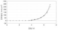
도 3은 장치 1(Device 1)의 전압-전류 밀도 특성을 2회 평가한 결과 얻은 그래프를 각각 도시한 것이다.
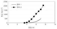
도 4는 장치 1(Device 1) 및 장치 2(Device 2)의 전압-휘도 특성을 나타낸 그래프를 각각 도시한 것이다.1 is a schematic cross-sectional view of a structure of an organic light emitting device according to an embodiment.
2 is a schematic cross-sectional view of a structure of an organic light emitting device according to another embodiment.
3 is a graph showing results obtained by evaluating voltage-current density characteristics of Device 1 twice.
4 is a graph illustrating voltage-luminance characteristics of device 1 and
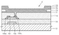
도 1은 일 구현예에 따른 유기 발광 장치의 단면을 개략적으로 도시한 단면도이다.1 is a schematic cross-sectional view of an organic light emitting device according to an embodiment.
상기 유기 발광 장치는, 기판(101) 상에 형성되며, 소스 전극(109a) 및 드레인 전극(109b), 산화물 반도체층(107), 게이트 전극(103), 및 상기 게이트 전극(103)을 상기 소스 전극(109a) 및 드레인 전극(109b)과 절연시키는 게이트 절연층(105)을 포함한 박막 트랜지스터를 포함한다. 상기 박막 트랜지스터 상에는 제1절연층(110)이 형성되어 있다. 또한, 상기 제1절연층(110) 상에 형성되며 상기 박막 트랜지스터의 드레인 전극(109b)와 연결된 캐소드(121)가 형성되어 있고, 화소 정의막(123)에 의하여 화소 영역이 정의되어 있다. 상기 캐소드(121) 상부로는 제1층(125), 유기층(127), 및 애노드(129)가 차례로 적층되어 있다.The organic light emitting device is formed on a
상기 기판(101)으로는, 통상적인 유기 발광 장치에서 사용되는 기판을 사용할 수 있는데, 기계적 강도, 열적 안정성, 투명성, 표면 평활성, 취급용이성 및 방수성이 우수한 유리 기판 또는 투명 플라스틱 기판을 사용할 수 있다.As the
게이트 전극(103)은 일반적인 전극 물질(예를 들면, 금속 등)로 형성될 수 있다. 예를 들어, 상기 게이트 전극(103)은 알루미늄(Al), 하프늄(Hf), 지르코늄(Zr), 아연(Zn), 텅스턴(W), 코발트(Co), 금(Au), 백금(Pt), 루테늄(Ru), 이리듐(Ir), 티타늄(Ti), 탄탈(Ta), 니켈(Ni), 은(Ag), 몰리브덴(Mo), 구리(Cu), 팔라듐(Pd), 인듐(In), 주석(Sn), 이들 중 2 이상의 조합(합금, 단순 혼합물 등을 포함함), 이들 중 1 이상의 원소를 포함하는 산화물(예를 들면, 인듐 틴 옥사이드(ITO), 인듐 아연 옥사이드(IZO) 등) 등일 수 있으나, 이에 한정되는 것은 아니다.The
게이트 절연층(105)은 게이트 전극(103)을 덮어 게이트 전극(103)을 소스 전극(109a) 및 드레인 전극(109b)과 절연시킬 수 있다. 상기 게이트 절연층(105)은 실리콘 산화물층이나 실리콘 질화물층일 수 있으나, 그 밖의 다른 물질층, 예컨대, 실리콘 질화물층보다 유전상수가 큰 고유전물질층일 수 있다. 게이트 절연층(105)는 실리콘 산화물층, 실리콘 질화물층 및 고유전물질층 중 적어도 두 층 이상이 적층된 구조를 가질 수도 있다.The
상기 산화물 반도체층(107) 중 산화물 반도체는 밴드갭(band gap)이 가시광 영역의 광 에너지보다 커서, 가시광을 실질적으로 흡수하지 않을 수 있다. 따라서, 상기 산화물 반도체층(107)을 구비한 박막 트랜지스터는 가시광 흡수에 따른 누설 전류 증가가 실질적으로 일어나지 않을 수 있다.The oxide semiconductor of the
상기 산화물 반도체층(107)은 아연-함유 산화물을 포함할 수 있다. 예를 들면, 상기 산화물 반도체층(107)은 ZnO를 포함할 수 있다.The
상기 아연-삼유 산화물은 제1성분을 더 포함하되, 상기 제1성분이 Hf, Y, Ta, Zr, Ga, Al, In, Fe, Sc, Lu, Yb, Tm, Er, Ho, Y, Mn, Co, Ni, Ti, Ge, Cu, Mo, Sn, 및 이들 중 2 이상의 조합으로 이루어진 군으로부터 선택될 수 있다.The zinc-trioxide oxide further includes a first component, wherein the first component is Hf, Y, Ta, Zr, Ga, Al, In, Fe, Sc, Lu, Yb, Tm, Er, Ho, Y, Mn , Co, Ni, Ti, Ge, Cu, Mo, Sn, and combinations of two or more thereof.
예를 들어, 상기 산화물 반도체층(107)은 Zn-Ga-O계 물질, Zn-In-O계 물질, Zn-In-Ga-O계 물질, Zn-Sn-O계 물질, 또는 Hf-In-Zn-O계 물질일 수 있으나, 이에 한정되는 것은 아니다.For example, the
게이트 절연층(105) 상에 산화물 반도체층(107)의 양단에 각각 접촉되는 소스 전극(109a) 및 드레인 전극(109b)이 구비되어 있다. 상기 소스 전극(109a) 및 드레인 전극(109b)은 단일 금속층 또는 다중 금속층일 수 있다. 소스 전극(109a) 및 드레인 전극(109b) 형성용 물질은 상기 게이트 전극(103) 형성용 물질을 참조할 수 있다.The
상술한 바와 같은 박막 트랜지스터의 제조 방법은 공지된 다양한 방법을 참조할 수 있다.The method of manufacturing the thin film transistor as described above may refer to various known methods.
도 1 중 제1절연층(110)은 상술한 바와 같은 박막 트랜지스터를 덮도록 형성될 수 있다. 상기 제1절연층(110)은 보호막 및/또는 평탄화막의 역할을 할 수도 있다. 상기 제1절연층(110)은 실리콘 산화물층이나 실리콘 질화물층일 수 있으나, 그 밖의 다른 물질층, 예컨대, 실리콘 질화물층보다 유전상수가 큰 고유전물질층일 수 있다. 제1절연층(110)는 실리콘 산화물층, 실리콘 질화물층 및 고유전물질층 중 적어도 두 층 이상이 적층된 구조를 가질 수도 있다. 상기 제1절연층(110)은 코팅법, 증착법, 스퍼터링법 등과 같은 공지된 다양한 방법을 이용하여 형성될 수 있다.In FIG. 1, the first insulating
상기 제1절연층(110) 상에는 캐소드(121)가 구비되어 있다. 상기 캐소드(121)는 비아홀을 통하여 드레인 전극(109b)과 전기적으로 연결되어 있다. 상기 캐소드(121)는 제1층(125)를 경유하여 유기층(127)에 전자를 주입하는 전극이다.The
상기 캐소드(121)는, 예를 들면, 리튬, 나트륨, 칼륨, 루비듐, 세슘 등의 알칼리 금속, 베릴륨, 마그네슘, 칼슘, 스트론튬, 바륨 등의 알칼리 토금속; 알루미늄, 스칸듐, 바나듐, 아연, 이트륨, 인듐, 세륨, 사마륨, 유로퓸, 테르븀, 이테르븀 등의 금속; 이들 중 2개 이상의 합금; 또는 이들 중 1개 이상과 금, 은, 백금, 구리, 망간, 티탄, 코발트, 니켈, 텅스텐, 주석 중 1개 이상과의 합금; 및 이들 중 2 이상의 조합을 포함할 수 있다. 상기 조합은 상술한 바와 같은 원소들 중 2 이상을 포함하는 합금, 상술한 바와 같은 원소들을 각각 포함한 다층 구조체 등을 포함한다. 합금으로서는, 예를 들면 마그네슘-은 합금, 마그네슘-인듐 합금, 마그네슘-알루미늄 합금, 인듐-은 합금, 리튬-알루미늄 합금, 리튬-마그네슘 합금, 리튬-인듐 합금, 칼슘-알루미늄 합금 등을 들 수 있다. 예를 들어, 상기 캐소드(121)는 Mg, Al, Ca, In, Ag, 및 이들 중 2 이상의 조합으로 이루어진 군으로부터 선택된 물질을 포함할 수 있으나, 이에 한정되는 것은 아니다. 또는, 상기 캐소드(121)는 ITO(인듐 틴 옥사이드), IZO(인듐 징크 옥사이드), 징크 산화물 등과 같은 상술한 바와 같은 금속 및 이들 중 2 이상의 합금의 산화물 등으로 형성될 수도 있다. 상기 캐소드(121)는 공지된 다양한 방법, 예를 들면, 증착법, 스퍼터링법 등을 이용하여 형성될 수 있다.The
상기 캐소드(121) 양단으로는 화소 영역을 정의하는 화소 정의막(123)이 형성되어 있다. 상기 화소 정의막(12)은 통상적인 유기 절연물 등으로 형성될 수 있다.A
상기 캐소드 (121) 상에는 제1층(123)이 구비되어 있다.The
상기 제1층(123)은 금속, 금속 황화물, 금속 산화물, 금속 질화물, 및 이들 중 2 이상의 조합으로 이루어진 군으로부터 선택된 제1물질을 포함할 수 있다.The
상기 제1물질은 2.6 eV 내지 4.6 eV 범위의 일함수, 예를 들면, 2.6 eV 내지 4.2 eV 범위의 일함수를 가질 수 있다. 상술한 바를 만족할 경우, 캐소드(121)로부터의 전자 주입이 효과적으로 이루어질 수 있어, 고효율 및 고휘도의 유기 발광 장치를 구현할 수 있다.The first material may have a work function in the range of 2.6 eV to 4.6 eV, for example, a work function in the range of 2.6 eV to 4.2 eV. When the above is satisfied, electron injection from the
상기 제1물질은 예를 들면, K, Rb, Cs, Mg, Sr, Ba, Sc, Y, Ti, Mn, Zn, Yb, K 황화물, Rb 황화물, Cs 황화물, Mg 황화물, Sr 황화물, Ba 황화물, Sc 황화물, Y 황화물, Ti 황화물, Mn 황화물, Zn 황화물, Yb 황화물, K 산화물, Rb 산화물, Cs 산화물, Mg 산화물, Sr 산화물, Ba 산화물, Sc 산화물, Y 산화물, Ti 산화물, Mn 산화물, Zn 산화물, Yb 산화물, K 질화물, Rb 질화물, Cs 질화물, Mg 질화물, Sr 질화물, Ba 질화물, Sc 질화물, Y 질화물, Ti 질화물, Mn 질화물, Zn 질화물, Yb 질화물, 및 이들 중 2 이상의 조합으로 이루어진 군으로부터 선택될 수 있다. 상기 "2 이상의 조합"은 예를 들면, 서로 다른 금속을 2 이상 포함한 물질(예를 들면, Ba-Cs-O계 물질)일 수도 있고, O, S 및 N 중 2 이상을 포함한 물질(예를 들면, Zn-O-N계 물질)일 수도 있다.The first material is, for example, K, Rb, Cs, Mg, Sr, Ba, Sc, Y, Ti, Mn, Zn, Yb, K sulfide, Rb sulfide, Cs sulfide, Mg sulfide, Sr sulfide, Ba sulfide , Sc sulfide, Y sulfide, Ti sulfide, Mn sulfide, Zn sulfide, Yb sulfide, K oxide, Rb oxide, Cs oxide, Mg oxide, Sr oxide, Ba oxide, Sc oxide, Y oxide, Ti oxide, Mn oxide, Zn Oxide, Yb oxide, K nitride, Rb nitride, Cs nitride, Mg nitride, Sr nitride, Ba nitride, Sc nitride, Y nitride, Ti nitride, Mn nitride, Zn nitride, Yb nitride, and combinations of two or more of these Can be selected from. The "combination of two or more" may be, for example, a material containing two or more different metals (for example, a Ba-Cs-O-based material), and a material containing two or more of O, S, and N (for example, Zn-ON based material).
상기 제1물질은 제1층(125)의 일함수 조절을 위하여 후술하는 바와 같이 다양하게 변형될 수 있다.The first material may be variously modified as described below for adjusting the work function of the
예를 들어, 상기 제1물질은, ZnS를 포함할 수 있다.For example, the first material may include ZnS.
또는, 상기 제1물질은, Sc2O3, CsO, BaO, 및 RbO으로 이루어진 군으로부터 선택될 수 있다.Alternatively, the first material may be selected from the group consisting of Sc2 O3 , CsO, BaO, and RbO.
또는, 상기 제1물질은, Y 황화물, Yb 황화물, Rb 황화물, Sr 황화물, Cs 황화물, Ba 황화물, Ti 황화물, Mn 황화물, Y 산화물, Yb 산화물, Rb 산화물, Sr 산화물, Cs 산화물, Ba 산화물, Ti 산화물, Mn 산화물, Y 질화물, Yb 질화물, Rb 질화물, Sr 질화물, Cs 질화물, Ba 질화물, Ti 질화물, 및 Mn 질화물로 이루어진 군으로부터 선택될 수 있다.Alternatively, the first material may be Y sulfide, Yb sulfide, Rb sulfide, Sr sulfide, Cs sulfide, Ba sulfide, Ti sulfide, Mn sulfide, Y oxide, Yb oxide, Rb oxide, Sr oxide, Cs oxide, Ba oxide, Ti oxide, Mn oxide, Y nitride, Yb nitride, Rb nitride, Sr nitride, Cs nitride, Ba nitride, Ti nitride, and Mn nitride.
또는, 상기 제1물질은 ZnS 및 Sc2O3 중 하나 이상과 Mg 황화물, Y 황화물, Yb 황화물, Mg 산화물, Y 산화물, Yb 산화물, Mg 질화물, Y 질화물, 및 Yb 질화물로 이루어진 군으로부터 선택된 하나 이상을 동시에 포함할 수 있다.Alternatively, the first material is at least one of ZnS and Sc2 O3 and one selected from the group consisting of Mg sulfide, Y sulfide, Yb sulfide, Mg oxide, Y oxide, Yb oxide, Mg nitride, Y nitride, and Yb nitride The above may be included simultaneously.
또는, 상기 제1물질은 ZnS 및 Sc2O3 중 하나 이상과 Mg, Y, 및 Yb로 이루어진 군으로부터 선택된 하나 이상을 동시에 포함할 수 있다.Alternatively, the first material may include at least one of ZnS and Sc2 O3 and at least one selected from the group consisting of Mg, Y, and Yb.
또는, 상기 제1물질은 Ti 황화물, Ti 산화물, Ti 질화물, Mn 황화물, Mn 산화물, 및 Mn 질화물 중 하나 이상과 Y 황화물, Yb 황화물, Rb 황화물, Cs 황화물, Ba 황화물, K 황화물, Y 산화물, Yb 산화물, Rb 산화물, Cs 산화물, Ba 산화물, K 산화물, Y 질화물, Yb 질화물, Rb 질화물, Cs 질화물, Ba 질화물, 및 K 질화물 중 하나 이상을 동시에 포함할 수 있으나, 이에 한정되는 것은 아니다.Alternatively, the first material may be at least one of Ti sulfide, Ti oxide, Ti nitride, Mn sulfide, Mn oxide, and Mn nitride and Y sulfide, Yb sulfide, Rb sulfide, Cs sulfide, Ba sulfide, K sulfide, Y oxide, One or more of Yb oxide, Rb oxide, Cs oxide, Ba oxide, K oxide, Y nitride, Yb nitride, Rb nitride, Cs nitride, Ba nitride, and K nitride may be simultaneously included, but is not limited thereto.
상기 제1층(125)은 상술한 바와 같은 제1물질 외에, 전자 주입 물질을 더 포함할 수 있다. 상기 전자 주입 물질은 유기 발광 소자의 전자 주입층 형성용 물질로서 공지된 임의의 물질 중에서 선택될 수 있다.The
예를 들어, 상기 전자 주입 물질은 LiF, NaCl, CsF, Li2O 및 BaF2으로 이루어진 군으로부터 선택될 수 있으나, 이에 한정되는 것은 아니다. 상기 전자 주입 물질은 예를 들면, LiF일 수 있으나, 이에 한정되는 것은 아니다.For example, the electron injection material may be selected from the group consisting of LiF, NaCl, CsF, Li2 O, and BaF2 , but is not limited thereto. The electron injection material may be, for example, LiF, but is not limited thereto.
예를 들어, 상기 제1층(125)은 제1물질 외에 전자 주입 물질을 더 포함하되, 상기 제1물질은 ZnS이고, 상기 전자 주입 물질은 LiF일 수 있다.For example, the
상기 제1층(125)이 전자 주입 물질을 더 포함할 경우, 상기 제1물질과 상기 전자 주입 물질의 중량비는 사용한 제1물질의 종류, 사용한 전자 주입 물질의 종류 등에 따라 상이할 것이나, 예를 들면, 10:1 내지 1:10, 구체적으로는 4:1 내지 1:4 일 수 있다.When the
상기 제1층(125)의 두께는 3 nm 내지 30 nm, 예를 들면, 5 nm 내지 20 nm일 수 있다. 상기 제1층(125)의 두께가 상술한 바와 같은 범위를 만족할 경우, 구동 전압의 상승없이 우수한 전자 주입 성능을 얻을 수 있다.The thickness of the
상기 제1층(125)은 증착법(예를 들면, 열증착) 또는 스퍼터링법을 이용하여 형성될 수 있다.The
예를 들면, 상기 제1물질 형성용 물질을 증착(예를 들면, 열증착) 또는 스퍼터링시킴으로써, 상기 제1층(125)을 형성할 수 있다.For example, the
본 명세서 중 "제1물질 형성용 물질"이란 상술한 바와 같은 제1물질 자체 또는 상술한 바와 같은 제1물질에 포함된 원소를 포함한 물질로서, 증착 또는 스퍼터링의 소스로 사용될 수 있는 물질을 가리키는 것이다. 예를 들어, 제1물질로서 ZnS를 포함한 제1층을 스퍼터링법을 이용하여 형성할 경우, 상기 제1물질 형성용 물질은 ZnS 타겟일 수 있고, 또는 Zn 타겟과 S 타겟일 수 있으며, 이는 당업자에게 용이하게 인식가능한 것이다.As used herein, "a material for forming a first material" refers to a material including an element included in the first material as described above or the first material as described above, and which may be used as a source of deposition or sputtering. . For example, when the first layer including ZnS as the first material is formed by the sputtering method, the material for forming the first material may be a ZnS target, or may be a Zn target and an S target, which is a person skilled in the art. It is easily recognizable to.
또한, 상기 제1층(125)이 제1물질 외에 전자 주입 물질을 더 포함할 경우, 상술한 바와 같은 제1물질 형성용 물질과 함께 전자 주입 물질을 증착 또는 스퍼터링시킴으로써, 제1층(125)을 형성할 수 있다.In addition, when the
예를 들면, ZnS와 LiF를 공증착시킴으로써, 제1층(125)을 형성할 수 있다.For example, the
상기 제1층(125) 상에는 유기층(127)이 형성될 수 있다. 상기 유기층(127)은 유기 발광 소자 분야에서 공지된 구조, 물질, 층 두께 등을 갖는 정공 저지층, 발광층, 정공 수송층 및 정공 주입층 중 하나 이상의 층을 포함할 수 있다. 상기 유기층(127)에 포함되는 물질은 유기물만을 의미하는 것은 아니며, 금속 착물(예를 들면, 발광 도펀트로서 이리듐 착물 등) 등도 포함할 수 있다.The
예를 들어, 상기 유기층(127)은 고분자를 포함할 수 있다. 예를 들어, 상기 유기층(127)은 제1층(125) 상에 차례로 전자 수송층, 정공 저지층, 발광층, 정공 수송층, 및 정공 주입층으로 이루어진 군으로부터 선택된 하나 이상의 층을 더 포함할 수 있다.For example, the
상기 전자 수송층은 진공증착법 등에 의하여 형성되거나 전자 수송 물질 및 용매를 포함한 혼합물을 전자 수송층 형성 영역에 제공한 다음 이를 열처리하는 습식 공정에 의하여 형성될 수 있다. 상기 전자 수송 물질 및 용매를 포함한 혼합물을 전자 수송층 형성 영역에 제공하는 방법으로는, 스핀코팅법, 캐스트법, 잉크젯 프린팅법, LB(Langmuir Blodgett)법 등과 같은 다양한 방법을 이용할 수 있다.The electron transport layer may be formed by a vacuum deposition method or by a wet process of providing a mixture including an electron transport material and a solvent to an electron transport layer formation region and then heat treating the electron transport layer. As a method of providing the mixture including the electron transporting material and the solvent to the electron transporting layer formation region, various methods such as spin coating, casting, inkjet printing, and LB (Langmuir Blodgett) method may be used.
진공증착법에 의하여 전자 수송층을 형성하는 경우, 그 증착 조건은 전자 수송층의 재료로서 사용하는 화합물, 목적으로 하는 전자 수송층의 구조 및 열적 특성 등에 따라 다르지만, 예를 들면, 증착온도 100 내지 500℃, 진공도 10-8 내지 10-3torr, 증착속도 0.01 내지 100Å/sec 범위에서 적절히 선택할 수 있다.When the electron transport layer is formed by vacuum deposition, the deposition conditions vary depending on the compound used as the material of the electron transport layer, the structure and thermal properties of the target electron transport layer, and the like. 10-8 to 10-3 torr, the deposition rate can be appropriately selected from 0.01 to 100 Pa / sec range.
스핀코팅법을 이용하여 전자 수송층을 형성하는 경우, 그 코팅 조건은 전자 수송층의 재료로서 사용하는 화합물, 목적하는 전자 수송층의 구조 및 열적 특성에 따라 상이하지만, 약 2000rpm 내지 5000rpm의 코팅 속도, 코팅 후 용매 제거를 위한 열처리 온도는 약 80℃ 내지 300℃의 온도 범위에서 적절히 선택할 수 있다.When the electron transport layer is formed by spin coating, the coating conditions are different depending on the compound used as the material of the electron transport layer, the structure and thermal properties of the desired electron transport layer, and a coating rate of about 2000 rpm to 5000 rpm, after coating The heat treatment temperature for the solvent removal may be appropriately selected in the temperature range of about 80 ℃ to 300 ℃.
상기 전자 수송층 재료로는 공지된 전자 수송 재료를 사용할 수 있는데, 예를 들면, Bphen(4,7-디페닐-1,10-페난트롤린(4,7-diphenyl-1,10-phenanthroline)), BAlq(하기 화학식 참조), 트리스(8-퀴놀리노레이트)알루미늄(Alq3), 베릴륨 비스(벤조퀴놀리-10-노에이트)(beryllium bis(benzoquinolin-10-olate: Bebq2), TPBi(하기 화학식 참조) 등과 같은 공지의 재료를 사용할 수 있다.As the electron transporting layer material, a known electron transporting material may be used. For example, Bphen (4,7-diphenyl-1,10-phenanthroline (4,7-diphenyl-1,10-phenanthroline)) , BAlq (see formula below), tris (8-quinolinorate) aluminum (Alq3), beryllium bis (benzoquinolin-10-olate: Bebq2 ), TPBi (below) Known materials such as chemical formulas) can be used.


TPBiTPBi
상기 전자수송층의 두께는 약 100Å 내지 1000Å, 예를 들면, 200Å 내지 500Å일 수 있다. 상기 전자수송층의 두께가 상술한 바와 같은 범위를 만족할 경우, 구동전압 상승 없이 만족스러운 전자 수송 특성을 얻을 수 있다.The electron transport layer may have a thickness of about 100 kPa to 1000 kPa, for example, 200 kPa to 500 kPa. When the thickness of the electron transport layer satisfies the above range, satisfactory electron transport characteristics may be obtained without increasing the driving voltage.
상기 정공 저지층은 형성 방법은 상술한 바와 같은 전자 수송층 형성 방법을 참조한다. 상기 정공 저지층 재료로는 공지의 정공저지재료, 예를 들면 옥사디아졸 유도체나 트리아졸 유도체, 페난트롤린 유도체, TAZ(하기 화학식 참조) 등을 들 수 있으나, 이에 한정되는 것은 아니다.The hole blocking layer is formed by the above-described method for forming an electron transporting layer. The hole blocking layer material may be a known hole blocking material, for example, an oxadiazole derivative, a triazole derivative, a phenanthroline derivative, or a TAZ (see the following chemical formula), but is not limited thereto.

상기 정공저지층의 두께는 약 50Å 내지 1000Å, 예를 들면 100Å 내지 300Å일 수 있다. 상기 정공저지층의 두께가 상술한 바와 같은 범위를 만족할 경우, 만족스러운 정공 저지 특성을 얻을 수 있다.The hole blocking layer may have a thickness of about 50 kPa to 1000 kPa, for example, 100 kPa to 300 kPa. When the thickness of the hole blocking layer satisfies the above range, satisfactory hole blocking characteristics can be obtained.
상기 발광층은 하나의 발광 물질을 포함하거나, 호스트와 도펀트의 조합을 포함할 수 있다. 공지의 호스트의 예로는 Alq3, CBP(4,4'-N,N'-디카바졸-비페닐), PVK(폴리(n-비닐카바졸)), 9,10-디(나프탈렌-2-일)안트라센(ADN), TCTA, TPBI(1,3,5-트리스(N-페닐벤즈이미다졸-2-일)벤젠(1,3,5-tris(N-phenylbenzimidazole-2-yl)benzene)), TBADN(3-tert-부틸-9,10-디(나프트-2-일) 안트라센), E3, DSA(디스티릴아릴렌) 등을 사용할 수 있으나, 이에 한정되는 것은 아니다.The light emitting layer may include one light emitting material or a combination of a host and a dopant. Examples of known hosts include Alq3 , CBP (4,4'-N, N'-dicarbazole-biphenyl), PVK (poly (n-vinylcarbazole)), 9,10-di (naphthalene-2- I) anthracene (ADN), TCTA, TPBI (1,3,5-tris (N-phenylbenzimidazol-2-yl) benzene (1,3,5-tris (N-phenylbenzimidazole-2-yl) benzene) ), TBADN (3-tert-butyl-9,10-di (naphth-2-yl) anthracene), E3, DSA (distyrylarylene) and the like can be used, but is not limited thereto.


PVKADNPVK ADN
한편, 공지된 적색 도펀트로서 PtOEP, Ir(piq)3, Btp2Ir(acac) 등을 이용할 수 있으나, 이에 한정되는 것은 아니다.On the other hand, PtOEP, Ir (piq)3 , Btp2 Ir (acac) and the like can be used as a known red dopant, but is not limited thereto.

또한, 공지된 녹색 도펀트로서, Ir(ppy)3(ppy = 페닐피리딘), Ir(ppy)2(acac), Ir(mpyp)3 등을 이용할 수 있으나, 이에 한정되는 것은 아니다.In addition, as the known green dopant, Ir (ppy)3 (ppy = phenylpyridine), Ir (ppy)2 (acac), Ir (mpyp)3, or the like may be used, but is not limited thereto.

한편, 공지된 청색 도펀트로서, F2Irpic, (F2ppy)2Ir(tmd), Ir(dfppz)3, ter-플루오렌(fluorene), 4,4'-비스(4-디페닐아미노스타릴) 비페닐 (DPAVBi), 2,5,8,11-테트라-티-부틸 페릴렌 (TBPe) 등을 이용할 수 있으나, 이에 한정되는 것은 아니다.On the other hand, as a known blue dopant, F2 Irpic, (F2 ppy)2 Ir (tmd), Ir (dfppz)3 , ter-fluorene, 4,4'-bis (4-diphenylaminostar Aryl) biphenyl (DPAVBi), 2,5,8,11-tetra-ti -butyl perylene (TBPe) and the like, but are not limited thereto.


DPAVBi TBPe DPAVBi TBPe
상기 발광층이 호스트 및 도펀트를 포함할 경우, 도펀트의 함량은 통상적으로 호스트 약 100 중량부를 기준으로 하여 약 0.01 내지 약 15 중량부의 범위에서 선택될 수 있으며, 이에 한정되는 것은 아니다.When the light emitting layer includes a host and a dopant, the content of the dopant may be generally selected from about 0.01 to about 15 parts by weight based on about 100 parts by weight of the host, but is not limited thereto.
상기 발광층의 두께는 약 100Å 내지 약 1000Å, 예를 들면 약 200Å 내지 약 600Å일 수 있다. 상기 발광층의 두께가 전술한 바와 같은 범위를 만족할 경우, 실질적인 구동 전압 상승없이 우수한 발광 특성을 나타낼 수 있다.The light emitting layer may have a thickness of about 100 kPa to about 1000 kPa, for example, about 200 kPa to about 600 kPa. When the thickness of the light emitting layer satisfies the aforementioned range, the light emitting layer may exhibit excellent light emission characteristics without a substantial increase in driving voltage.
상기 정공 수송층 재료로는 공지된 임의의 정공 수송 재료를 사용할 수 있는데, 예를 들면, N,N'-비스(3-메틸페닐)-N,N'-디페닐-[1,1-비페닐]-4,4'-디아민(TPD), N,N'-디(나프탈렌-1-일)-N,N'-디페닐 벤지딘(NPD), NPB(N, N'-diphenyl-N, N'-bis(1-naphthyl)-(1,1'-biphenyl)-4, 4'-diamine, N,N'-디페닐-N,N'-비스(1-나프틸)-(1,1'-비페닐)-4,4'-디아민) 등을 사용할 수 있다.Any hole transport material known in the art may be used as the hole transport layer material. For example, N, N'-bis (3-methylphenyl) -N, N'-diphenyl- [1,1-biphenyl] -4,4'-diamine (TPD), N, N'-di (naphthalen-1-yl) -N, N'-diphenyl benzidine (NPD), NPB (N, N'-diphenyl-N, N ' -bis (1-naphthyl)-(1,1'-biphenyl) -4, 4'-diamine, N, N'-diphenyl-N, N'-bis (1-naphthyl)-(1,1 ' -Biphenyl) -4,4'-diamine) etc. can be used.
상기 정공 수송층의 두께는 약 50Å 내지 1000Å, 예를 들면 100Å 내지 600Å일 수 있다. 상기 정공수송층의 두께가 상술한 범위를 만족할 경우, 구동전압의 상승없이 만족스러운 정도의 정공 수송 특성을 얻을 수 있다. 상기 정공 수송층은 1층 이상의 구조를 가질 수 있다.The hole transport layer may have a thickness of about 50 kPa to 1000 kPa, for example, 100 kPa to 600 kPa. When the thickness of the hole transport layer satisfies the above-described range, it is possible to obtain a satisfactory hole transport characteristic without increasing the driving voltage. The hole transport layer may have a structure of one or more layers.
상기 정공 주입층 재료로는 공지된 임의의 정공 주입 재료를 사용할 수 있는데, 예를 들면, m-MTDATA [4,4',4''-tris (3-methylphenylphenylamino) triphenylamine, 하기 화학식 참조], TDATA(하기 화학식 참조), 2T-NATA(하기 화학식 참조), Pani/DBSA (Polyaniline/Dodecylbenzenesulfonic acid:폴리아닐린/도데실벤젠술폰산, 하기 화학식 참조), PEDOT/PSS(Poly(3,4-ethylenedioxythiophene)/Poly(4-styrenesulfonate):폴리(3,4-에틸렌디옥시티오펜)/폴리(4-스티렌술포네이트), 하기 화학식 참조), Pani/CSA (Polyaniline/Camphor sulfonicacid:폴리아닐린/캠퍼술폰산) 또는 PANI/PSS (Polyaniline)/Poly(4-styrenesulfonate):폴리아닐린)/폴리(4-스티렌술포네이트)) 등을 사용할 수 있으나, 이에 한정되는 것은 아니다.As the hole injection layer material, any hole injection material known in the art may be used. For example, m-MTDATA [4,4 ′, 4 ''-tris (3-methylphenylphenylamino) triphenylamine (see the following Chemical Formula), TDATA (See formula below), 2T-NATA (see formula below), Pani / DBSA (Polyaniline / Dodecylbenzenesulfonic acid: polyaniline / dodecylbenzenesulfonic acid, see formula below), PEDOT / PSS (Poly (3,4-ethylenedioxythiophene) / Poly (4-styrenesulfonate): poly (3,4-ethylenedioxythiophene) / poly (4-styrenesulfonate), see formula below), Pani / CSA (Polyaniline / Camphor sulfonicacid: polyaniline / camphorsulfonic acid) or PANI / PSS (Polyaniline) / Poly (4-styrenesulfonate): polyaniline) / poly (4-styrenesulfonate)) and the like may be used, but is not limited thereto.


Pani/DBSA PEDOT/PSS
Pani / DBSA PEDOT / PSS
상기 정공주입층의 두께는 약 100Å 내지 10000Å, 예를 들면, 100Å 내지 1000Å일 수 있다. 상기 정공주입층의 두께가 상술한 바를 만족할 경우, 구동 전압의 상승없이 만족스러운 정공주입 특성을 얻을 수 있다.The hole injection layer may have a thickness of about 100 kPa to 10000 kPa, for example, 100 kPa to 1000 kPa. When the thickness of the hole injection layer satisfies the above, satisfactory hole injection characteristics may be obtained without increasing the driving voltage.
상기 유기층(127)은 공지된 다양한 방법을 이용하여 형성될 수 있다. 예를 들면, 상기 유기층(127)은 증착법, 스퍼터링법 등을 이용하여 형성될 수 있다. 또는 상기 유기층(127)이 고분자를 포함할 경우, 습식 공정을 이용하여 형성될 수도 있다.The
예를 들면, 상기 유기층(127)이 발광층을 포함하고, 상기 발광층이 상기 제1층(125) 상부에 형성될 경우, 임의의 발광 고분자 및 용매를 포함하는 혼합물을 상기 제1층(125) 상부에 제공한 다음, 이를 열처리함으로써 발광 고분자를 포함한 발광층을 형성할 수 있다. 여기서, 상기 발광 고분자 및 용매를 포함하는 혼합물을 상기 제1층(125) 상부에 제공하는 방법으로는, 스핀 코팅, 스프레잉, 잉크젯 프린팅, 디핑, 캐스팅, 그라비아 코팅, 바코팅, 롤코팅, 와이어 바 코팅, 스크린 코팅, 플렉소 코팅, 또는 오프셋 코팅을 이용할 수 있으나, 이에 한정되는 것은 아니다. 이 때, 상기 제1층(125)은 상기 제1물질(선택적으로 전자 주입 물질을 더 포함할 수 있음)을 포함하고, 및/또는 상술한 바와 같이 증착(예를 들면, 열증착) 또는 스퍼터링법을 이용하여 형성될 수 있으므로, 발광층 형성을 위하여 상기 발광 고분자 및 용매를 포함하는 혼합물을 상기 제1층(125) 상부에 제공하더라도, 제1층(125)이 상기 용매에 의하여 실질적으로 손상되지 않는다. 따라서, 상기 제1층(125)과 발광층 사이의 계면에는 상기 제1층(125)에 포함된 물질(즉, 상술한 바와 같은 제1물질과, 선택적으로는 전자 주입 물질)과 발광층에 포함된 물질(즉, 발광 고분자)이 공존하는 인터믹싱(intermixing) 영역이 실질적으로 존재하지 않을 수 있으며, 제1층(125)이 우수한 표면 특성을 유지할 수 있는 바, 우수한 전기적 특성을 확보하면서도 대면적 제작 용이성과 공정 안정성이 확보된 유기 발광 장치를 효과적으로 제작할 수 있다.For example, when the
상기 유기층(127) 상부로는 애노드(129)가 구비되어 있다. 상기 애노드(129)는 정공을 유기층(127)에 주입하는 전극이다.An
상기 애노드(129)는 산화 인듐, 산화아연, 산화주석, 및 이들의 복합체인 ITO, IZO 등과 같은 산화물 또는 금, 백금, 은, 구리 등을 이용할 수 있으나, 이에 한정되는 것은 아니다. 예를 들어, 상기 애노드(129)로서 ITO를 사용할 경우, 그 두께는 1000 내지 2000Å일 수 있다. 또는, 상기 애노드(129)로서 Ag를 사용할 경우, 그 두께는 150 내지 250Å일 수 있다.The
상기 애노드(129)는 공지된 다양한 방법, 예를 들면, 증착법, 스퍼터링법 등을 이용하여 형성될 수 있으나, 이에 한정되는 것은 아니다.The
도 2는 다른 구현예에 따른 유기 발광 장치를 개략적으로 도시한 단면도이다. 도 2의 유기 발광 장치는 제1층(125)과 캐소드(121) 사이에 전자 주입층(123)이 개재되어 있다는 점을 제외하고는 상기 도 1에 도시된 유기 발광 장치와 동일한 구조를 갖는 바, 이는 도 1에 대한 설명을 참조한다.2 is a schematic cross-sectional view of an organic light emitting device according to another embodiment. The organic light emitting device of FIG. 2 has the same structure as the organic light emitting device of FIG. 1 except that the
상기 전자 주입층(123)은 제1층(125)과 캐소드(121) 사이에 개재되어 캐소드(121)로부터 제1층(125)로의 전자가 효과적으로 주입될 수 있도록 한다.The
상기 전자 주입층(123)은 임의의 전자 주입 물질을 포함할 수 있다. 예를 들어, 상기 전자 주입층(123)은 LiF, NaCl, CsF, Li2O 및 BaF2으로 이루어진 군으로부터 선택된 하나 이상을 포함할 수 있으나, 이에 한정되는 것은 아니다. 상기 전자 주입층(123)은, 예를 들면, LiF를 포함할 수 있다.The
상기 전자 주입층(123)은 공지된 다양한 방법, 예를 들면, 증착법, 스퍼터링법 등을 이용하여 형성될 수 있다.The
상기 전자 주입층(123)의 두께는 0.1nm 내지 10nm, 예를 들면, 0.5nm 내지 5nm일 수 있다. 상기 전자 주입층(123)의 두께가 상술한 바와 같은 범위를 만족할 경우, 구동 전압 상승없이 만족스러운 전자 주입 성능을 얻을 수 있다.The thickness of the
한편, Hf-In-Zn-O계 산화물 반도체층을 구비한 박막 트랜지스터가 구비된 n-Type 형 기판 상에 Al층(캐소드, 700Å)/LiF층(전자 주입층, 10Å)/ZnS층(제1층, 250Å)/ (ADN + DPVBi)층 (발광층, 300Å, 도펀트인 DPVBi의 도핑 농도는 4중량%임)/NPB층(정공 수송층, 150Å)/ MTDATA층 (정공 주입층, 700Å)/ITO층(애노드, 1000 내지 2000Å)가 차례로 적층되어 있는 유기 발광 장치(이하,"장치 1" (Device 1)이라 함)를 제작하여, 상기 장치 1의 전류 밀도, 효율, 전력 효율, 휘도, 및 색좌표를 PR650 휘도계 Spectroscan Source Measurement Unit.(PhotoReaserch)와 Keithely 236(IVL 측정시 이용함)를 이용하여 평가하였다. 여기서, 상기 제1층은 열증착법을 이용하여 형성하였다. 도 3은 장치 1의 전류 밀도 특성을 2회 측정한 결과 수득한 그래프를 각각 도시한 도면이다.On the other hand, an Al layer (cathode, 700 kV) / LiF layer (electron injection layer, 10 kV) / ZnS layer (prepared on an n-type substrate having a thin film transistor having an Hf-In-Zn-O-based oxide semiconductor layer) 1 layer, 250 Å) / (ADN + DPVBi) layer (light emitting layer, 300 Å, dopant DPVBi doping concentration is 4% by weight) / NPB layer (hole transport layer, 150 Å) / MTDATA layer (hole injection layer, 700 Å) / ITO An organic light emitting device (hereinafter referred to as "Device 1") in which layers (anodes, 1000 to 2000 microseconds) are stacked in order is fabricated, and the current density, efficiency, power efficiency, luminance, and color coordinates of the device 1 are obtained. Were evaluated using a PR650 luminance meter Spectroscan Source Measurement Unit. (PhotoReaserch) and Keithely 236 (used for IVL measurements). Here, the first layer was formed using a thermal evaporation method. 3 is a graph showing the graphs obtained by measuring the current density characteristics of the apparatus 1 twice.
한편, 상기 장치 1의 구동 전압별 전류 밀도, 효율, 전력 효율, 휘도 및 색좌표는 하기 표 1을 참조한다:On the other hand, the current density, efficiency, power efficiency, luminance and color coordinates for each driving voltage of the device 1 refer to Table 1 below:
(V)Driving voltage
(V)
(mA/cm2)Current density
(mA / cm2 )
(Cd/A)efficiency
(Cd / A)
(Im/W)Power efficiency
(Im / W)
(Cd/m2)Luminance
(Cd / m2 )
도 3 및 표 1로부터 상기 장치 1은 우수한 전기적 특성을 가짐을 확인할 수 있다.3 and Table 1 it can be seen that the device 1 has excellent electrical properties.
한편, 제1층으로서 250Å의 ZnS층 형성하는 대신, ZnS과 LiF를 공증착(ZnS와 LiF의 중량비는 1:1임)하여 ZnS 및 LiF를 포함한 제1층(250Å)을 형성하였다는 점을 제외하고는 상기 장치 1과 동일한 구성을 갖는 유기 발광 장치(이하, "장치 2"(Device 2)라 함)를 제작하였다.Meanwhile, instead of forming a 250 ns ZnS layer as the first layer, ZnS and LiF were co-deposited (the weight ratio of ZnS and LiF is 1: 1) to form a first layer (250 ns) including ZnS and LiF. Except for the device 1, an organic light emitting device (hereinafter, referred to as “
한편, 상기 장치 2의 전류 밀도, 효율, 전력 효율, 휘도 및 색좌표는 하기 표 2를 참조한다:On the other hand, the current density, efficiency, power efficiency, brightness and color coordinates of the
(V)Driving voltage
(V)
(mA/cm2)Current density
(mA / cm2 )
(Cd/A)efficiency
(Cd / A)
(Im/W)Power efficiency
(Im / W)
(Cd/m2)Luminance
(Cd / m2 )
상기 표 2로부터 상기 장치 2는 우수한 전기적 특성을 가짐을 확인할 수 있다.It can be seen from Table 2 that the
또한, Hf-In-Zn-O계 산화물 반도체층을 구비한 박막 트랜지스터가 구비된 n-Type 형 기판 상에 Al층(캐소드, 1500Å)/LiF층(전자 주입층, 10Å)/ZnS층(제1층, 250Å)/Bebq2층(전자수송층, 250Å)/(ADN + DPVBi)층 (발광층, 300Å, 도펀트인 DPVBi의 도핑 농도는 4중량%임)/NPB층(정공 수송층, 150Å)/ MTDATA층 (정공 주입층, 700Å)/ITO층(애노드, 1000 내지 2000Å)가 차례로 적층되어 있는 유기 발광 장치(이하, "장치 3"(Device 3)이라 함) 및 Hf-In-Zn-O계 산화물 반도체층을 구비한 박막 트랜지스터가 구비된 n-Type 형 기판 상에 Al층(캐소드, 1500Å)/LiF층(전자 주입층, 10Å)/ZnS층(제1층, 250Å)/Bebq2층(전자수송층, 250Å)/(ADN + DPVBi)층 (발광층, 300Å, 도펀트인 DPVBi의 도핑 농도는 4중량%임)/NPB층(제1정공 수송층, 50Å)/NPB층(제2정공 수송층, 200Å)/PEDOT:PSS층(정공 주입층, 600Å)/ITO층(애노드, 1000 내지 2000Å)가 차례로 적층되어 있는 유기 발광 장치(이하, "장치 4" (Device 4)이라 함)를 제작하여, 상기 장치 1의 전류 밀도, 효율, 전력 효율, 휘도, 및 색좌표를 PR650 휘도계 Spectroscan Source Measurement Unit.(PhotoReaserch)와 Keithely 236(IVL 측정시 이용함)를 이용하여 평가하였다. 상기 장치 4 중 제2정공 수송층은 NPB 및 유기 용매를 포함한 혼합물을 제1정공 수송층 상부에 제공한 후 열처리하여 형성한 것이고, 정공 주입층은 PEDOT:PSS 용액을 제2정공 수송층 상부에 제공한 후 열처리하여 형성한 것이다.In addition, an Al layer (cathode, 1500 mV) / LiF layer (electron injection layer, 10 mV) / ZnS layer 1 layer, 250Å) / Bebq2 layer (electron transport layer, 250Å) / (ADN + DPVBi) layer (light emitting layer, 300Å, dopant DPVBi doping concentration is 4% by weight) / NPB layer (hole transport layer, 150Å) / MTDATA layer (Hole injection layer, 700 GPa) / ITO layer (anode, 1000 to 2000 GPa) organic light emitting device (hereinafter referred to as "device 3") and Hf-In-Zn-O-based oxide semiconductor Al layer (cathode, 1500Å) / LiF layer (electron injection layer, 10Å) / ZnS layer (first layer, 250Å) / Bebq2 layer (electron transport layer,) on n-type substrate with thin film transistor 250 μs) / (ADN + DPVBi) layer (light emitting layer, 300 μs, dopant DPVBi doping concentration is 4% by weight) / NPB layer (first hole transport layer, 50 μs) / NPB layer (second hole transport layer, 200 μs) / PEDOT : PSS layer (hole injection layer, 600 GPa) / ITO layer (anode, 1000 to 2000 GPa) An organic light emitting device (hereinafter referred to as "device 4") stacked in sequence is fabricated, and the current density, efficiency, power efficiency, luminance, and color coordinates of the device 1 are measured using a PR650 luminance meter Spectroscan Source Measurement Unit. (PhotoReaserch) and Keithely 236 (used for IVL measurement). In the
(V)Driving voltage
(V)
(mA/cm2)Current density
(mA / cm2 )
(Cd/A)efficiency
(Cd / A)
(Lm/W)Power efficiency
(Lm / W)
(Cd/m2)Luminance
(Cd / m2 )
Device 3
상기 표 3로부터 상기 장치 3 및 4는 우수한 전기적 특성을 가짐을 확인할 수 있다.It can be seen from Table 3 that the
101: 기판
109a: 소스 전극
109b: 드레인 전극
107: 산화물 반도체층
103: 게이트 전극
105: 게이트 절연층
110: 제1절연층
121: 캐소드
123: 화소 정의막
125: 제1층
127: 유기층
129:애노드101: substrate
109a: source electrode
109b: drain electrode
107: oxide semiconductor layer
103: gate electrode
105: gate insulating layer
110: first insulating layer
121: cathode
123: pixel defining layer
125: first layer
127: organic layer
129: anode
Claims (16)
Translated fromKorean상기 기판 상에 형성되며, 소스 전극 및 드레인 전극, 산화물 반도체층, 게이트 전극, 및 상기 게이트 전극을 상기 소스 전극 및 드레인 전극과 절연시키는 게이트 절연층을 포함한 박막 트랜지스터;
상기 박막 트랜지스터 상에 형성된 제1절연층;
상기 제1절연층 상에 형성되며 상기 박막 트랜지스터의 소스 전극 및 드레인 전극 중 하나와 연결된 캐소드;
상기 캐소드 상에 형성되며, 금속, 금속 황화물, 금속 산화물, 금속 질화물, 및 이들 중 2 이상의 조합으로 이루어진 군으로부터 선택된 제1물질을 포함한 제1층;
상기 제1층 상에 형성된 유기층; 및
상기 유기층 상에 형성된 애노드;
를 포함한 유기 발광 장치.Board;
A thin film transistor formed on the substrate, the thin film transistor including a source electrode and a drain electrode, an oxide semiconductor layer, a gate electrode, and a gate insulating layer insulating the gate electrode from the source electrode and the drain electrode;
A first insulating layer formed on the thin film transistor;
A cathode formed on the first insulating layer and connected to one of a source electrode and a drain electrode of the thin film transistor;
A first layer formed on the cathode and comprising a first material selected from the group consisting of metals, metal sulfides, metal oxides, metal nitrides, and combinations of two or more thereof;
An organic layer formed on the first layer; And
An anode formed on the organic layer;
Organic light emitting device including.
상기 산화물 반도체층이 아연-함유 산화물을 포함한 것을 특징으로 하는 유기 발광 장치.The method of claim 1,
And the oxide semiconductor layer comprises a zinc-containing oxide.
상기 아연-함유 산화물은 제1성분을 더 포함하고, 상기 제1성분이 Hf, Y, Ta, Zr, Ga, Al, In, Fe, Sc, Lu, Yb, Tm, Er, Ho, Y, Mn, Co, Ni, Ti, Ge, Cu, Mo, Sn, 및 이들 중 2 이상의 조합으로 이루어진 군으로부터 선택된 것을 특징으로 하는 유기 발광 장치.The method of claim 1,
The zinc-containing oxide further comprises a first component, wherein the first component is Hf, Y, Ta, Zr, Ga, Al, In, Fe, Sc, Lu, Yb, Tm, Er, Ho, Y, Mn , Co, Ni, Ti, Ge, Cu, Mo, Sn, and an organic light emitting device, characterized in that selected from the group consisting of two or more thereof.
상기 캐소드가 Mg, Al, Ca, In, Ag, 및 이들 중 2 이상의 조합으로 이루어진 군으로부터 선택된 물질을 포함한 것을 특징으로 하는 유기 발광 장치.The method of claim 1,
And the cathode comprises a material selected from the group consisting of Mg, Al, Ca, In, Ag, and combinations of two or more thereof.
상기 제1물질이 2.6 eV 내지 4.6 eV 범위의 일함수를 갖는 것을 특징으로 하는 유기 발광 장치.The method of claim 1,
And the first material has a work function in the range of 2.6 eV to 4.6 eV.
상기 제1물질이, K, Rb, Cs, Mg, Sr, Ba, Sc, Y, Ti, Mn, Zn, Yb, K 황화물, Rb 황화물, Cs 황화물, Mg 황화물, Sr 황화물, Ba 황화물, Sc 황화물, Y 황화물, Ti 황화물, Mn 황화물, Zn 황화물, Yb 황화물, K 산화물, Rb 산화물, Cs 산화물, Mg 산화물, Sr 산화물, Ba 산화물, Sc 산화물, Y 산화물, Ti 산화물, Mn 산화물, Zn 산화물, Yb 산화물, K 질화물, Rb 질화물, Cs 질화물, Mg 질화물, Sr 질화물, Ba 질화물, Sc 질화물, Y 질화물, Ti 질화물, Mn 질화물, Zn 질화물, Yb 질화물, 및 이들 중 2 이상의 조합으로 이루어진 군으로부터 선택된 것을 특징으로 하는 유기 발광 장치.The method of claim 1,
The first substance is K, Rb, Cs, Mg, Sr, Ba, Sc, Y, Ti, Mn, Zn, Yb, K sulfide, Rb sulfide, Cs sulfide, Mg sulfide, Sr sulfide, Ba sulfide, Sc sulfide , Y sulfide, Ti sulfide, Mn sulfide, Zn sulfide, Yb sulfide, K oxide, Rb oxide, Cs oxide, Mg oxide, Sr oxide, Ba oxide, Sc oxide, Y oxide, Ti oxide, Mn oxide, Zn oxide, Yb Oxides, K nitrides, Rb nitrides, Cs nitrides, Mg nitrides, Sr nitrides, Ba nitrides, Sc nitrides, Y nitrides, Ti nitrides, Mn nitrides, Zn nitrides, Yb nitrides, and combinations of two or more thereof An organic light emitting device.
상기 제1층이 전자 주입 물질을 더 포함한 것을 특징으로 하는 유기 발광 장치.The method of claim 1,
And the first layer further comprises an electron injection material.
상기 제1층의 두께가 3 nm 내지 30 nm인 것을 특징으로 하는 유기 발광 장치.The method of claim 1,
The thickness of the first layer is an organic light emitting device, characterized in that 3 nm to 30 nm.
상기 제1층과 상기 캐소드 사이에 전자 주입층이 개재된 것을 특징으로 하는 유기 발광 장치.The method of claim 1,
And an electron injection layer interposed between the first layer and the cathode.
상기 박막 트랜지스터 상에 제1절연층을 형성하는 단계;
상기 제1절연층 상에 박막 트랜지스터의 소스 전극 및 드레인 전극 중 하나와 연결된 캐소드를 형성하는 단계;
증착법 또는 스퍼터링법을 이용하여 상기 캐소드 상에 금속, 금속 황화물, 금속 산화물, 금속 질화물, 및 이들 중 2 이상의 조합으로 이루어진 군으로부터 선택된 제1물질을 포함한 제1층을 형성하는 단계;
상기 제1층 상에 유기층을 형성하는 단계; 및
상기 유기층 상에 애노드를 형성하는 단계;
를 포함하는 유기 발광 장치의 제조 방법.Forming a thin film transistor including a source electrode and a drain electrode, an oxide semiconductor layer, a gate electrode, and a gate insulating layer insulating the gate electrode from the source electrode and the drain electrode;
Forming a first insulating layer on the thin film transistor;
Forming a cathode connected to one of a source electrode and a drain electrode of the thin film transistor on the first insulating layer;
Forming a first layer comprising a first material selected from the group consisting of metals, metal sulfides, metal oxides, metal nitrides, and combinations of two or more thereof on the cathode using deposition or sputtering;
Forming an organic layer on the first layer; And
Forming an anode on the organic layer;
Method for manufacturing an organic light emitting device comprising a.
상기 산화물 반도체층이 제1성분을 더 포함하고, 상기 제1성분이 Hf, Y, Ta, Zr, Ga, Al, In, Fe, Sc, Lu, Yb, Tm, Er, Ho, Y, Mn, Co, Ni, Ti, Ge, Cu, Mo, 및 이들 중 2 이상의 조합으로 이루어진 군으로부터 선택된 것을 특징으로 하는 유기 발광 장치의 제조 방법.The method of claim 10,
The oxide semiconductor layer further comprises a first component, wherein the first component is Hf, Y, Ta, Zr, Ga, Al, In, Fe, Sc, Lu, Yb, Tm, Er, Ho, Y, Mn, Co, Ni, Ti, Ge, Cu, Mo, and a method for manufacturing an organic light emitting device, characterized in that selected from the group consisting of two or more thereof.
상기 제1물질이 2.6 eV 내지 4.6 eV 범위의 일함수를 갖는 것을 특징으로 하는 유기 발광 장치의 제조 방법.The method of claim 10,
And the first material has a work function in the range of 2.6 eV to 4.6 eV.
상기 제1물질이, K, Rb, Cs, Mg, Sr, Ba, Sc, Y, Ti, Mn, Zn, Yb, K 황화물, Rb 황화물, Cs 황화물, Mg 황화물, Sr 황화물, Ba 황화물, Sc 황화물, Y 황화물, Ti 황화물, Mn 황화물, Zn 황화물, Yb 황화물, K 산화물, Rb 산화물, Cs 산화물, Mg 산화물, Sr 산화물, Ba 산화물, Sc 산화물, Y 산화물, Ti 산화물, Mn 산화물, Zn 산화물, Yb 산화물, K 질화물, Rb 질화물, Cs 질화물, Mg 질화물, Sr 질화물, Ba 질화물, Sc 질화물, Y 질화물, Ti 질화물, Mn 질화물, Zn 질화물, Yb 질화물, 및 이들 중 2 이상의 조합으로 이루어진 군으로부터 선택된 것을 특징으로 하는 유기 발광 장치의 제조 방법.The method of claim 10,
The first substance is K, Rb, Cs, Mg, Sr, Ba, Sc, Y, Ti, Mn, Zn, Yb, K sulfide, Rb sulfide, Cs sulfide, Mg sulfide, Sr sulfide, Ba sulfide, Sc sulfide , Y sulfide, Ti sulfide, Mn sulfide, Zn sulfide, Yb sulfide, K oxide, Rb oxide, Cs oxide, Mg oxide, Sr oxide, Ba oxide, Sc oxide, Y oxide, Ti oxide, Mn oxide, Zn oxide, Yb Oxides, K nitrides, Rb nitrides, Cs nitrides, Mg nitrides, Sr nitrides, Ba nitrides, Sc nitrides, Y nitrides, Ti nitrides, Mn nitrides, Zn nitrides, Yb nitrides, and combinations of two or more thereof The manufacturing method of the organic light emitting device characterized by the above-mentioned.
제1물질 형성용 물질과 함께 전자 주입 물질을 증착 또는 스퍼터링함으로써 상기 제1층 형성 단계를 수행하는 것을 특징으로 하는 유기 발광 장치의 제조 방법.The method of claim 10,
And forming the first layer by depositing or sputtering an electron injection material together with a material for forming a first material.
상기 제1층 형성 단계 전에, 상기 캐소드 상에 전자 주입층을 형성하는 단계를 수행하는 것을 특징으로 하는 유기 발광 장치의 제조 방법.The method of claim 10,
Before forming the first layer, forming an electron injection layer on the cathode.
상기 유기층 형성 단계를 스핀 코팅, 스프레잉, 잉크젯 프린팅, 디핑, 캐스팅, 그라비아 코팅, 바코팅, 롤코팅, 와이어 바 코팅, 스크린 코팅, 플렉소 코팅, 또는 오프셋 코팅을 이용하여 수행하는 것을 특징으로 하는 유기 발광 장치의 제조 방법.The method of claim 10,
The organic layer forming step is performed using spin coating, spraying, inkjet printing, dipping, casting, gravure coating, bar coating, roll coating, wire bar coating, screen coating, flexographic coating, or offset coating. Method of manufacturing an organic light emitting device.
Priority Applications (3)
| Application Number | Priority Date | Filing Date | Title |
|---|---|---|---|
| KR20100032286AKR20110112992A (en) | 2010-04-08 | 2010-04-08 | Organic light emitting device and method for manufacturing same |
| JP2011085120AJP2011223001A (en) | 2010-04-08 | 2011-04-07 | Organic light-emitting device and manufacturing method thereof |
| US13/064,670US20110248259A1 (en) | 2010-04-08 | 2011-04-07 | Organic light emitting device and method of manufacturing the same |
Applications Claiming Priority (1)
| Application Number | Priority Date | Filing Date | Title |
|---|---|---|---|
| KR20100032286AKR20110112992A (en) | 2010-04-08 | 2010-04-08 | Organic light emitting device and method for manufacturing same |
Publications (1)
| Publication Number | Publication Date |
|---|---|
| KR20110112992Atrue KR20110112992A (en) | 2011-10-14 |
Family
ID=44760280
Family Applications (1)
| Application Number | Title | Priority Date | Filing Date |
|---|---|---|---|
| KR20100032286ACeasedKR20110112992A (en) | 2010-04-08 | 2010-04-08 | Organic light emitting device and method for manufacturing same |
Country Status (3)
| Country | Link |
|---|---|
| US (1) | US20110248259A1 (en) |
| JP (1) | JP2011223001A (en) |
| KR (1) | KR20110112992A (en) |
Cited By (1)
| Publication number | Priority date | Publication date | Assignee | Title |
|---|---|---|---|---|
| KR20170033968A (en)* | 2015-09-17 | 2017-03-28 | 삼성디스플레이 주식회사 | Organic light emitting device |
Families Citing this family (3)
| Publication number | Priority date | Publication date | Assignee | Title |
|---|---|---|---|---|
| TWI474479B (en)* | 2011-11-30 | 2015-02-21 | Au Optronics Corp | Organic light emitting display structure and organic light emitting display |
| KR101668030B1 (en)* | 2014-08-21 | 2016-10-21 | 삼성디스플레이 주식회사 | Organic light emitting diode and organic light emitting display device including the same |
| WO2022064580A1 (en)* | 2020-09-24 | 2022-03-31 | シャープ株式会社 | Light emitting element and display device |
Family Cites Families (5)
| Publication number | Priority date | Publication date | Assignee | Title |
|---|---|---|---|---|
| EP1144197B1 (en)* | 1999-01-15 | 2003-06-11 | 3M Innovative Properties Company | Thermal Transfer Method. |
| EP1770788A3 (en)* | 2005-09-29 | 2011-09-21 | Semiconductor Energy Laboratory Co., Ltd. | Semiconductor device having oxide semiconductor layer and manufacturing method thereof |
| KR100659105B1 (en)* | 2005-11-03 | 2006-12-19 | 삼성에스디아이 주식회사 | Organic light emitting display device |
| JP2009123696A (en)* | 2007-10-26 | 2009-06-04 | Mitsubishi Chemicals Corp | Organic electroluminescent device, image display device, and organic electroluminescent device manufacturing method |
| JP4907714B2 (en)* | 2009-11-16 | 2012-04-04 | 大日本印刷株式会社 | Organic electroluminescence device |
- 2010
- 2010-04-08KRKR20100032286Apatent/KR20110112992A/ennot_activeCeased
- 2011
- 2011-04-07JPJP2011085120Apatent/JP2011223001A/enactivePending
- 2011-04-07USUS13/064,670patent/US20110248259A1/ennot_activeAbandoned
Cited By (1)
| Publication number | Priority date | Publication date | Assignee | Title |
|---|---|---|---|---|
| KR20170033968A (en)* | 2015-09-17 | 2017-03-28 | 삼성디스플레이 주식회사 | Organic light emitting device |
Also Published As
| Publication number | Publication date |
|---|---|
| JP2011223001A (en) | 2011-11-04 |
| US20110248259A1 (en) | 2011-10-13 |
Similar Documents
| Publication | Publication Date | Title |
|---|---|---|
| KR101097339B1 (en) | Organic light emitting diode and method for preparing the same | |
| EP2012375B1 (en) | Organic light emitting device | |
| KR101927941B1 (en) | Organic light-emitting diode comprising multi-layered hole transporting layer, and flat display device including the same | |
| KR100922757B1 (en) | Organic light emitting device with improved lifespan | |
| KR100922760B1 (en) | Organic light emitting device | |
| EP2999019B1 (en) | Organic light-emitting diode including an electron transport layer stack comprising different lithium compounds and elemental metal | |
| KR102688407B1 (en) | Electronic device and method for preparing the same | |
| EP2365556B1 (en) | Light-emitting element, light-emitting device, electronic device, and lighting device | |
| EP3164898B1 (en) | Organic light-emitting diode (oled) including an electron transport layer stack comprising different lithium compounds | |
| JP5048145B2 (en) | ORGANIC LIGHT EMITTING ELEMENT AND METHOD FOR PRODUCING ORGANIC LIGHT EMITTING ELEMENT | |
| EP3035400B1 (en) | Organic light-emitting diode comprising electron transport layers with different matrix compounds | |
| KR102081281B1 (en) | Organic light emitting device | |
| KR101156428B1 (en) | Organic light emitting device | |
| US10522778B2 (en) | Organic light-emitting diode including an electronic transport layer comprising a three component blend of a matrix compound and two lithium compounds | |
| KR20100011290A (en) | A method for preparing an organic light emitting device and am organic light emitting device | |
| KR20210104788A (en) | Organic light emitting devices, methods of making them, and compositions for use therein | |
| KR102685868B1 (en) | Display device including common charge generation layer and method of manufacturing same | |
| US20240107793A1 (en) | Sheet resistance component | |
| KR102726233B1 (en) | Active OLED display | |
| KR20110112992A (en) | Organic light emitting device and method for manufacturing same | |
| KR20130112601A (en) | Polymer blend, organic light emitting diodes using the same and method for controlling charge mobility of the emitting layer of thereof | |
| KR20090125616A (en) | Organic light emitting device manufacturing method and organic light emitting device | |
| KR102017745B1 (en) | Organic light-emitting diode, method for preparing the same, and organic light-emitting devise including the same | |
| KR20210115255A (en) | Thin film, method of manufacturing the same and light emitting device including the same | |
| KR102872632B1 (en) | Active-matrix oled display |
Legal Events
| Date | Code | Title | Description |
|---|---|---|---|
| PA0109 | Patent application | Patent event code:PA01091R01D Comment text:Patent Application Patent event date:20100408 | |
| PG1501 | Laying open of application | ||
| N231 | Notification of change of applicant | ||
| PN2301 | Change of applicant | Patent event date:20120725 Comment text:Notification of Change of Applicant Patent event code:PN23011R01D | |
| A201 | Request for examination | ||
| PA0201 | Request for examination | Patent event code:PA02012R01D Patent event date:20150209 Comment text:Request for Examination of Application Patent event code:PA02011R01I Patent event date:20100408 Comment text:Patent Application | |
| E902 | Notification of reason for refusal | ||
| PE0902 | Notice of grounds for rejection | Comment text:Notification of reason for refusal Patent event date:20160109 Patent event code:PE09021S01D | |
| E601 | Decision to refuse application | ||
| PE0601 | Decision on rejection of patent | Patent event date:20160527 Comment text:Decision to Refuse Application Patent event code:PE06012S01D Patent event date:20160109 Comment text:Notification of reason for refusal Patent event code:PE06011S01I |