KR20110096464A - Multiple gas supply device and plasma processing device having the same - Google Patents
Multiple gas supply device and plasma processing device having the sameDownload PDFInfo
- Publication number
- KR20110096464A KR20110096464AKR1020100015918AKR20100015918AKR20110096464AKR 20110096464 AKR20110096464 AKR 20110096464AKR 1020100015918 AKR1020100015918 AKR 1020100015918AKR 20100015918 AKR20100015918 AKR 20100015918AKR 20110096464 AKR20110096464 AKR 20110096464A
- Authority
- KR
- South Korea
- Prior art keywords
- gas supply
- central
- peripheral
- plasma
- supply unit
- Prior art date
- Legal status (The legal status is an assumption and is not a legal conclusion. Google has not performed a legal analysis and makes no representation as to the accuracy of the status listed.)
- Granted
Links
Images


Classifications
- H—ELECTRICITY
- H01—ELECTRIC ELEMENTS
- H01L—SEMICONDUCTOR DEVICES NOT COVERED BY CLASS H10
- H01L21/00—Processes or apparatus adapted for the manufacture or treatment of semiconductor or solid state devices or of parts thereof
- H01L21/67—Apparatus specially adapted for handling semiconductor or electric solid state devices during manufacture or treatment thereof; Apparatus specially adapted for handling wafers during manufacture or treatment of semiconductor or electric solid state devices or components ; Apparatus not specifically provided for elsewhere
- H01L21/67005—Apparatus not specifically provided for elsewhere
- H01L21/67011—Apparatus for manufacture or treatment
- H01L21/67017—Apparatus for fluid treatment
- H01L21/67063—Apparatus for fluid treatment for etching
- H01L21/67069—Apparatus for fluid treatment for etching for drying etching
- H—ELECTRICITY
- H01—ELECTRIC ELEMENTS
- H01J—ELECTRIC DISCHARGE TUBES OR DISCHARGE LAMPS
- H01J37/00—Discharge tubes with provision for introducing objects or material to be exposed to the discharge, e.g. for the purpose of examination or processing thereof
- H01J37/32—Gas-filled discharge tubes
- H01J37/32009—Arrangements for generation of plasma specially adapted for examination or treatment of objects, e.g. plasma sources
- H01J37/32082—Radio frequency generated discharge
- H01J37/321—Radio frequency generated discharge the radio frequency energy being inductively coupled to the plasma
- H—ELECTRICITY
- H01—ELECTRIC ELEMENTS
- H01J—ELECTRIC DISCHARGE TUBES OR DISCHARGE LAMPS
- H01J37/00—Discharge tubes with provision for introducing objects or material to be exposed to the discharge, e.g. for the purpose of examination or processing thereof
- H01J37/32—Gas-filled discharge tubes
- H01J37/32431—Constructional details of the reactor
- H01J37/3244—Gas supply means
- H—ELECTRICITY
- H01—ELECTRIC ELEMENTS
- H01L—SEMICONDUCTOR DEVICES NOT COVERED BY CLASS H10
- H01L21/00—Processes or apparatus adapted for the manufacture or treatment of semiconductor or solid state devices or of parts thereof
- H01L21/02—Manufacture or treatment of semiconductor devices or of parts thereof
- H01L21/04—Manufacture or treatment of semiconductor devices or of parts thereof the devices having potential barriers, e.g. a PN junction, depletion layer or carrier concentration layer
- H01L21/18—Manufacture or treatment of semiconductor devices or of parts thereof the devices having potential barriers, e.g. a PN junction, depletion layer or carrier concentration layer the devices having semiconductor bodies comprising elements of Group IV of the Periodic Table or AIIIBV compounds with or without impurities, e.g. doping materials
- H01L21/30—Treatment of semiconductor bodies using processes or apparatus not provided for in groups H01L21/20 - H01L21/26
- H01L21/302—Treatment of semiconductor bodies using processes or apparatus not provided for in groups H01L21/20 - H01L21/26 to change their surface-physical characteristics or shape, e.g. etching, polishing, cutting
- H01L21/306—Chemical or electrical treatment, e.g. electrolytic etching
- H01L21/3065—Plasma etching; Reactive-ion etching
- H01L21/30655—Plasma etching; Reactive-ion etching comprising alternated and repeated etching and passivation steps, e.g. Bosch process
Landscapes
- Engineering & Computer Science (AREA)
- Physics & Mathematics (AREA)
- Plasma & Fusion (AREA)
- General Physics & Mathematics (AREA)
- Analytical Chemistry (AREA)
- Condensed Matter Physics & Semiconductors (AREA)
- Chemical & Material Sciences (AREA)
- Manufacturing & Machinery (AREA)
- Computer Hardware Design (AREA)
- Microelectronics & Electronic Packaging (AREA)
- Power Engineering (AREA)
- Drying Of Semiconductors (AREA)
- Plasma Technology (AREA)
Abstract
Translated fromKorean
Description
Translated fromKorean본 발명은 다중 가스공급장치 및 이를 구비한 플라즈마 처리장치에 관한 것으로, 구체적으로는 다중으로 공급되는 가스로 플라즈마를 유도하여 피처리 기판의 특정부를 깊게 에칭하는 방법에 관한 것이다.BACKGROUND OF THE
실리콘의 이방성 에칭 방법은 피처리 기판의 특정부를 에칭하고 에칭된 특정부에 패시베이션 층을 증착하는 과정을 반복적으로 수행한다. 에칭 및 증착 과정을 반복적으로 수행하면서 원하는 깊이 만큼 피처리 기판의 특정부를 에칭한다. 이러한 에칭 및 증착 과정은 플라즈마에 의해 이루어지게 된다.The anisotropic etching method of silicon repeatedly performs a process of etching a specific portion of a substrate to be processed and depositing a passivation layer on the etched specific portion. The specific portions of the substrate to be processed are etched to a desired depth while repeatedly performing the etching and deposition processes. This etching and deposition process is performed by the plasma.
플라즈마는 같은 수의 양이온(positive ions)과 전자(electrons)를 포함하는 고도로 이온화된 가스이다. 플라즈마 방전은 이온, 자유 래디컬, 원자, 분자를 포함하는 활성 가스를 발생하기 위한 가스 여기에 사용되고 있다. 활성 가스는 다양한 분야에서 널리 사용되고 있으며 집적 회로 장치, 액정 디스플레이, 태양 전지등과 같은 장치를 제조하기 위한 여러 반도체 제조 공정 예들 들어, 식각(etching), 증착(deposition), 세정(cleaning), 에싱(ashing) 등에 다양하게 사용된다.Plasma is a highly ionized gas containing the same number of positive ions and electrons. Plasma discharges are used for gas excitation to generate active gases containing ions, free radicals, atoms, molecules. Active gases are widely used in various fields and are used in various semiconductor manufacturing processes for manufacturing devices such as integrated circuit devices, liquid crystal displays, solar cells, etc., for example, etching, deposition, cleaning, and ashing. It is variously used for ashing.
플라즈마를 발생하기 위한 플라즈마 소스는 여러 가지가 있는데 무선 주파수(radio frequency)를 사용한 용량 결합 플라즈마(capacitive coupled plasma)와 유도 결합 플라즈마(inductive coupled plasma)가 그 대표적인 예이다. 용량 결합 플라즈마 소스는 정확한 용량 결합 조절과 이온 조절 능력이 높아서 타 플라즈마 소스에 비하여 공정 생산력이 높다는 장점을 갖는다. 그러나 대형화되는 피처리 기판을 처리하기 위하여 용량 결합 전극을 대형화하는 경우 전극의 열화에 의해 전극에 변형이 발생되거나 손상될 수 있다. 이러한 경우 전계 강도가 불균일하게 되어 플라즈마 밀도가 불균일하게 될 수 있으며 반응기 내부를 오염시킬 수 있다. 유도 결합 플라즈마 소스의 경우에도 유도 코일 안테나의 면적을 크게 하는 경우 마찬가지로 플라즈마 밀도를 균일하게 얻기가 어렵다.There are a number of plasma sources for generating plasma, and the representative examples are capacitive coupled plasma and inductive coupled plasma using radio frequency. Capacitively coupled plasma sources have the advantage of high process productivity compared to other plasma sources due to their high capacity for precise capacitive coupling and ion control. However, when the capacitively coupled electrode is enlarged in order to process an enlarged substrate, the electrode may be deformed or damaged by deterioration of the electrode. In this case, the electric field strength may be uneven, which may result in uneven plasma density and contaminate the inside of the reactor. In the case of an inductively coupled plasma source, it is also difficult to obtain a uniform plasma density when the area of the induction coil antenna is increased.
최근 반도체 제조 산업에서는 반도체 소자의 초미세화, 반도체 회로를 제조하기 위한 실리콘 웨이퍼 기판이나 유리 기판 또는 플라스틱 기판과 같은 피처리 기판의 대형화 그리고 새로운 처리 대상 물질의 개발되고 있는 등과 같은 여러 요인으로 인하여 더욱 향상된 플라즈마 처리 기술이 요구되고 있다. 특히, 대면적의 피처리 기판에 대한 우수한 처리 능력을 갖는 향상된 플라즈마 소스 및 플라즈마 처리 기술이 요구되고 있다. 더욱이 레이저를 이용한 다양한 반도체 제조 장치가 제공되고 있다. 레이저를 이용하는 반도체 제조 공정은 피처리 기판에 대한 증착, 식각, 어닐닝, 세정 등과 같은 다양한 공정에 넓게 적용되고 있다. 이와 같은 레이저를 이용한 반도체 제조 공정의 경우에도 상술한 문제점이 존재한다.In recent years, the semiconductor manufacturing industry has been further improved due to various factors such as ultra miniaturization of semiconductor devices, the enlargement of silicon wafer substrates or substrates to be processed such as glass or plastic substrates for manufacturing semiconductor circuits, and the development of new materials to be processed. Plasma treatment technology is required. In particular, there is a need for improved plasma sources and plasma processing techniques that have good processing capabilities for large area substrates. Furthermore, various semiconductor manufacturing apparatuses using lasers have been provided. Semiconductor manufacturing processes using lasers have been widely applied to various processes such as deposition, etching, annealing, cleaning, and the like on a substrate to be processed. In the case of a semiconductor manufacturing process using such a laser, the above-described problems exist.
피처리 기판의 대형화는 전체적인 생산 설비의 대형화를 야기하게 된다. 생산 설비의 대형화는 전체적인 설비 면적을 증가시켜 결과적으로 생산비를 증가시키는 요인이 된다. 그럼으로 가급적 설비 면적을 최소화 할 수 있는 플라즈마 반응기 및 플라즈마 처리 시스템이 요구되고 있다. 특히, 반도체 제조 공정에서는 단위 면적당 생산성이 최종 재품의 가격에 영향을 미치는 중요한 요인의 하나로 작용한다.The enlargement of the substrate to be processed causes the enlargement of the entire production equipment. Larger production facilities increase the overall plant area, resulting in increased production costs. Therefore, there is a need for a plasma reactor and a plasma processing system capable of minimizing the installation area. In particular, in the semiconductor manufacturing process, productivity per unit area is one of the important factors affecting the price of the final product.
또한 피처리 기판의 대형화로 인하여 피처리 기판의 중심영역과 주변영역은 플라즈마에 의해 균일하게 처리되지 못하는 문제가 발생한다. 즉, 플라즈마는 피처리 기판의 주변영역에 비해 중심영역으로 집중되어 형성되기 때문에 피처리 기판을 전체적으로 균일하게 처리하는데 어려움이 발생하였다.In addition, due to the larger size of the substrate, a problem arises in that the central region and the peripheral region of the substrate to be processed are not uniformly processed by the plasma. That is, since the plasma is concentrated in the center region compared to the peripheral region of the substrate, it is difficult to uniformly process the substrate.
본 발명의 목적은 대면적이면서 균일한 플라즈마를 다중으로 공급되는 공정가스와 중심 플라즈마소스 및 주변 플라즈마소스를 이용하여 형성함으로써 대형화되는 피처리 기판에 대한 처리 효율을 향상시킬 수 있는 다중 가스공급장치 및 이를 구비한 플라즈마 처리장치을 제공하는데 있다.An object of the present invention is to form a large area and uniform plasma by using a multi-process gas and the central plasma source and the surrounding plasma source to form a multi-gas supply apparatus that can improve the processing efficiency for the large sized substrate to be processed and The present invention provides a plasma processing apparatus having the same.
상기한 기술적 과제를 달성하기 위한 본 발명의 일면은 다중 가스공급장치 및 이를 구비한 플라즈마 처리장치에 관한 것이다. 본 발명의 다중 가스공급장치는 피처리 기판의 특정부를 에칭하는 단계; 및 상기 에칭된 특정부의 표면에 패시베이션층을 증착하는 단계;를 반복적으로 진행하여 상기 피처리 기판의 특정부 깊이를 증가시키면서 에칭하되, 상기 에칭 단계 또는 상기 증착 단계 중 어느 하나는 중심 플라즈마소스와 주변 플라즈마소스에 의해 형성된 플라즈마 존재하에서 실행되고, 중심 플라즈마소스에는 중심 가스공급부가 구비되고 주변 플라즈마소스에는 주변 가스공급부가 구비되어 공정가스를 공급한다.One aspect of the present invention for achieving the above technical problem relates to a multiple gas supply apparatus and a plasma processing apparatus having the same. The multiple gas supply apparatus of the present invention comprises the steps of etching a specific portion of the substrate to be processed; And depositing a passivation layer on the surface of the etched specific portion, repeatedly etching to increase the depth of the specific portion of the substrate to be processed, wherein either the etching step or the deposition step is performed around the central plasma source. It is executed in the presence of a plasma formed by the plasma source, the central plasma source is provided with a central gas supply unit and the peripheral plasma source is provided with a peripheral gas supply unit to supply the process gas.
일 실시예에 있어서, 상기 중심 가스 공급부 또는 상기 주변 가스 공급부는 복수 개의 가스 분사구를 포함하는 가스 샤워헤드로 형성된다.In one embodiment, the central gas supply unit or the peripheral gas supply unit is formed of a gas shower head including a plurality of gas injection holes.
일 실시예에 있어서, 상기 중심 가스 공급부와 상기 주변 가스 공급부는 상기 피처리 기판에 대하여 높이가 상이하게 배치된다.In one embodiment, the central gas supply portion and the peripheral gas supply portion are different in height with respect to the substrate to be processed.
일 실시예에 있어서, 상기 중심 가스 공급부와 상기 주변 가스 공급부는 가스 공급원으로부터 동일한 공정가스를 공급하거나 서로 다른 공정가스를 공급한다.In one embodiment, the central gas supply unit and the surrounding gas supply unit supply the same process gas or different process gases from a gas supply source.
본 발명의 다중 가스공급구조를 갖는 플라즈마 처리장치는 피처리 기판을 지지하기 위한 기판 지지대를 내부에 포함하는 반응기 몸체; 상기 반응기 몸체의 중심영역으로 공정가스를 공급하기 위한 중심 가스 공급부를 포함하는 중심 플라즈마소스; 상기 반응기 몸체의 주변영역으로 공정가스를 공급하기 위한 주변 가스 공급부를 포함하는 주변 플라즈마소스를 포함하여 상기 피처리 기판의 특정부를 에칭하고 에칭된 특정부의 표면에 패시베이션 층 증착하는 과정을 반복적으로 수행한다.Plasma processing apparatus having a multi-gas supply structure of the present invention includes a reactor body including a substrate support for supporting a substrate to be processed; A central plasma source including a central gas supply unit for supplying a process gas to a central region of the reactor body; Etching a specific portion of the substrate to be treated including a peripheral plasma source including a peripheral gas supply for supplying a process gas to the peripheral region of the reactor body and repeatedly depositing a passivation layer on the surface of the etched specific portion. .
일 실시예에 있어서, 상기 중심 가스 공급부와 상기 주변 가스 공급부는 복수 개의 가스 분사구를 포함하는 가스 샤워헤드로 형성된다.In one embodiment, the central gas supply and the peripheral gas supply is formed of a gas shower head including a plurality of gas injection holes.
일 실시예에 있어서, 상기 중심 가스 공급부와 상기 주변 가스 공급부는 상기 피처리 기판에 대하여 높이가 상이하게 배치되된다.In one embodiment, the central gas supply portion and the peripheral gas supply portion are arranged differently in height with respect to the substrate to be processed.
일 실시예에 있어서, 상기 처리장치는 반응기 몸체의 상부에 구비되어 중심영역 및 주변영역으로 분리되어 설치된 중심, 주변 무선 주파수 안테나; 상기 중심, 주변 무선 주파수 안테나의 하부에 각각 구비되어 자속을 통과시키기 위한 유전체 윈도우를 포함한다.In one embodiment, the processing device includes a central, peripheral radio frequency antenna provided in the upper portion of the reactor body is separated into a central region and a peripheral region; It is provided in the lower portion of the center, the surrounding radio frequency antenna and includes a dielectric window for passing the magnetic flux.
일 실시예에 있어서, 상기 유전체 윈도우는 상기 가스 분사구에 대응되는 복수 개의 가스 공급홀을 포함하는 것을 특징으로 하는 다중 가스공급장치를 구비한다.In one embodiment, the dielectric window is provided with a multi-gas supply device, characterized in that it comprises a plurality of gas supply holes corresponding to the gas injection port.
일 실시예에 있어서, 상기 중심 가스 공급부와 상기 주변 가스 공급부는 공정가스가 균일하게 공급되기 위한 배플을 포함한다.In one embodiment, the central gas supply unit and the surrounding gas supply unit includes a baffle for uniformly supplied process gas.
일 실시예에 있어서, 상기 중심 가스 공급부와 상기 주변 가스 공급부는 동일한 공정가스를 공급하거나 서로 다른 공정가스를 상기 반응기 몸체의 내부로 공급한다.In one embodiment, the central gas supply unit and the surrounding gas supply unit supplies the same process gas or different process gases into the reactor body.
일 실시예에 있어서, 상기 중심 무선 주파수 안테나에 전원을 공급하는 중심 전원 공급원과 상기 주변 무선 주파수 안테나에 전원을 공급하는 주변 전원공급원을 포함한다.In one embodiment, a central power source for supplying power to the central radio frequency antenna and a peripheral power supply for supplying power to the peripheral radio frequency antenna.
일 실시예에 있어서, 상기 중심 전원공급원과 상기 주변 전원공급원은 서로 다른 무선 주파수를 공급한다.In one embodiment, the central power supply and the peripheral power supply supply different radio frequencies.
일 실시예에 있어서, 상기 무선 주파수 안테나를 커버하며 자속 출입구가 상기 반응기 몸체의 내부로 향하도록 마련되는 마그네틱 코어 커버를 포함한다.In one embodiment, it comprises a magnetic core cover covering the radio frequency antenna and provided with a magnetic flux entry and exit toward the interior of the reactor body.
일 실시예에 있어서, 상기 중심 전원공급원은 1~5㎒의 주파수를 공급하고, 상기 주변 전원공급원은 1~500㎑의 주파수를 공급한다.In one embodiment, the central power supply supplies a frequency of 1-5 MHz, and the peripheral power supply supplies a frequency of 1-500 kHz.
일 실시예에 있어서, 상기 기판 지지대는 1~50㎒의 바이어스 전원을 공급하는 바이어스 전원 공급원에 연결된다.In one embodiment, the substrate support is connected to a bias power supply for supplying a bias power of 1-50 MHz.
본 발명의 다중 가스공급장치 및 이를 구비한 플라즈마 처리장치에 의하면, 중심 플라즈마소스와 주변 플라즈마소스가 구분되어 구비되고, 여기에 분리된 가스 공급부를 구비하므로 기판의 전영역에 걸쳐 균일하게 플라즈마 처리가 가능하다.According to the multiple gas supply apparatus and the plasma processing apparatus having the same of the present invention, since the central plasma source and the surrounding plasma source are provided separately, and the separated gas supply unit is provided, the plasma processing is uniformly distributed over the entire area of the substrate. It is possible.
또한, 중심 플라즈마소스와 주변 플라즈마소스 사이에 접지된 간섭 방지 전극을 이용하여 플라즈마 반응기 내부에 전기적 간섭이 없는 독립적인 다중 플라즈마 영역을 형성할 수 있다.In addition, by using an interference preventing electrode grounded between the central plasma source and the surrounding plasma source, an independent multiple plasma region without electrical interference may be formed in the plasma reactor.
또한 중심 플라즈마소스와 주변 플라즈마소스에 의해 형성된 플라즈마는 효율적으로 피처리 기판의 특정부를 깊게 에칭할 수 있다.In addition, the plasma formed by the central plasma source and the peripheral plasma source can efficiently etch a specific portion of the substrate to be processed efficiently.
도 1은 본 발명의 바람직한 실시예에 따라 다중 가스공급구조를 갖는 플라즈마 처리장치의 단면을 도시한 도면이다.
도 2는 본 발명의 플라즈마 처리장치에 설치되는 복수 개의 가스 공급홀이 구비된 유전체 윈도우의 평면을 도시한 도면이다.
도 3은 본 발명의 바람직한 실시예에 따라 중심 가스공급부와 주변 가스공급부에 각각 서로 다른 공정가스가 공급되는 플라즈마 처리장치의 단면을 도시한 도면이다.1 is a cross-sectional view of a plasma processing apparatus having a multiple gas supply structure according to a preferred embodiment of the present invention.
FIG. 2 is a diagram illustrating a plane of a dielectric window having a plurality of gas supply holes installed in the plasma processing apparatus of the present invention.
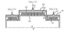
3 is a cross-sectional view of a plasma processing apparatus in which different process gases are supplied to a central gas supply unit and a peripheral gas supply unit according to a preferred embodiment of the present invention.
본 발명을 충분히 이해하기 위해서 본 발명의 바람직한 실시예를 첨부 도면을 참조하여 설명한다. 본 발명의 실시예는 여러 가지 형태로 변형될 수 있으며, 본 발명의 범위가 아래에서 상세히 설명하는 실시예로 한정되는 것으로 해석되어서는 안 된다. 본 실시예는 당업계에서 평균적인 지식을 가진 자에게 본 발명을 보다 완전하게 설명하기 위해서 제공 되어지는 것이다. 따라서 도면에서의 요소의 형상 등은 보다 명확한 설명을 강조하기 위해서 과장되어 표현될 수 있다. 각 도면에서 동일한 부재는 동일한 참조부호로 도시한 경우가 있음을 유의하여야 한다. 본 발명의 요지를 불필요하게 흐릴 수 있다고 판단되는 공지 기능 및 구성에 대한 상세한 기술은 생략된다.
In order to fully understand the present invention, preferred embodiments of the present invention will be described with reference to the accompanying drawings. Embodiment of the present invention may be modified in various forms, the scope of the invention should not be construed as limited to the embodiments described in detail below. This embodiment is provided to more completely explain the present invention to those skilled in the art. Therefore, the shape of the elements in the drawings and the like may be exaggerated to emphasize a more clear description. It should be noted that the same members in each drawing are sometimes shown with the same reference numerals. Detailed descriptions of well-known functions and configurations that are determined to unnecessarily obscure the subject matter of the present invention are omitted.
도 1은 본 발명의 바람직한 실시예에 따라 다중 가스공급구조를 갖는 플라즈마 처리장치의 단면을 도시한 도면이다.1 is a cross-sectional view of a plasma processing apparatus having a multiple gas supply structure according to a preferred embodiment of the present invention.
도 1에 도시된 바와 같이, 본 발명의 바람직한 플라즈마 처리장치는 반응기 몸체(11), 중심 플라즈마소스 및 주변 플라즈마소스로 구성된다. 반응기 몸체(11)는 내부에 피처리 기판(13)이 놓이는 기판 지지대(12)가 구비되고, 하부 측벽에 진공펌프(8)가 연결된다. 중심 플라즈마소스(20)는 반응기 몸체(11)의 상부에 구비되어 반응기 몸체(11) 내부의 중심영역으로 플라즈마를 형성한다. 주변 플라즈마소스(30)는 반응기 몸체(11) 내부의 주변영역으로 플라즈마를 형성한다. 이때 중심 플라즈마소스(20)와 주변 플라즈마소스(30)는 동일한 공정가스를 공급받아 플라즈마를 형성한다.
As shown in Fig. 1, the preferred plasma processing apparatus of the present invention is composed of a reactor body 11, a central plasma source and a peripheral plasma source. The reactor body 11 is provided with a
반응기 몸체(11)는 알루미늄, 스테인리스, 구리와 같은 금속 물질로 제작될 수 있다. 또는 코팅된 금속 예를 들어, 양극 처리된 알루미늄이나 니켈 도금된 알루미늄으로 제작될 수도 있다. 또는 탄소나노튜브가 공유 결합된 복합 금속을 사용할 수도 있다. 또는 내화 금속(refractory metal)로 제작될 수도 있다. 또 다른 대안으로 반응기 몸체(11)를 전체적 또는 부분적으로 석영, 세라믹과 같은 전기적 절연 물질로 제작하는 것도 가능하다. 이와 같이 반응기 몸체(11)는 의도된 플라즈마 프로세스가 수행되기에 적합한 어떠한 물질로도 제작될 수 있다. 반응기 몸체(11)의 구조는 피처리 기판(13)에 따라 그리고 플라즈마의 균일한 발생을 위하여 적합한 구조 예를 들어, 원형 구조나 사각형 구조 그리고 이외에도 어떠한 형태의 구조를 가질 수 있다. 피처리 기판(13)은 예를 들어, 반도체 장치, 디스플레이 장치, 태양전지 등과 같은 다양한 장치들의 제조를 위한 웨이퍼 기판, 유리 기판, 플라스틱 기판 등과 같은 기판들이다.The reactor body 11 may be made of a metal material such as aluminum, stainless steel, or copper. Or it may be made of coated metal, for example anodized aluminum or nickel plated aluminum. Alternatively, a composite metal in which carbon nanotubes are covalently bonded may be used. Alternatively, it may be made of refractory metal. As another alternative, it is also possible to fabricate the reactor body 11 in whole or in part with an electrically insulating material such as quartz, ceramic. As such, the reactor body 11 may be made of any material suitable for carrying out the intended plasma process. The structure of the reactor body 11 may have a structure suitable for uniform generation of the plasma, for example, a circular structure or a square structure, or any other structure depending on the
플라즈마 반응기(10)의 내부에는 피처리 기판(13)을 지지하기 위한 기판 지지대(12)가 구비된다. 기판 지지대(12)는 바이어스 전원 공급원(46)(서로 다른 무선 주파수 전원을 공급하는 두 개의 바이어스 전원 공급원이 연결될 수 있다)에 연결되어 바이어스 된다. 바이어스 전원 공급원(46)이 임피던스 정합기(48)(또는 각각의 임피던스 정합기)를 통하여 기판 지지대(12)에 전기적으로 연결된다. 또는 기판 지지대(12)는 바이어스 전원의 공급 없이 제로 퍼텐셜(zero potential)을 갖는 구조로 변형 실시될 수도 있다. 본 발명의 일 실시예에서는 바이어스 전원 공급원(46)에서 1~50㎒의 바이어스 전원을 공급하고, 13.56㎒의 바이어스 전원을 기판 지지대(12)에 공급하는 것이 바람직하다.The
그리고 기판 지지대(12)는 정전척을 포함할 수 있다. 또는 기판 지지대(12)는 히터를 포함할 수 있다. 기본적으로 기판 지지대(12)는 고정형 또는 수직으로 승하강이 가능한 구조로 구성된다. 또는 기판 지지대(12)는 전극 어셈블리와 평행하게 선형 또는 회전 이동 가능한 구조를 갖는다. 이러한 이동 가능한 구조에서 기판 지지대(12)를 선형 또는 회전 이동하기 위한 구동 메커니즘을 포함할 수 있다. 반응기 몸체(11)의 하부에 가스의 균일한 배기를 위하여 배기 배플(미도시)이 구성될 수 있다.
The
중심 플라즈마소스(20)와 주변 플라즈마소스(30)는 반응기 몸체(11)의 상부에 구비된다. 중심 플라즈마소스(20)와 주변 플라즈마소스(30) 사이는 전기적으로 절연될 수 있도록 절연구간(29)이 구비된다. 이때 절연구간(29)이 접지된 간섭방지전극으로 구성되어 중심 플라즈마소스(20)와 주변 플라즈마소스(30)간에 전기적으로 절연되어 분리된 플라즈마 영역을 갖도록 할 수 있다. 중심 플라즈마소스(20)는 반응기 몸체(11) 내부의 중심영역으로 플라즈마를 형성하고, 주변 플라즈마소스(30)는 반응기 몸체(11) 내부의 주변영역으로 플라즈마를 형성한다. 여기서, 중심 플라즈마소스(20)와 주변 플라즈마소스(30)는 가스 공급부와 무선 주파수 안테나(24, 34) 및 유전체 윈도우(26)가 구비된다. 가스 공급부는 중심 플라즈마소스(20)에 구비되는 중심 가스 공급부(60)와 주변 플라즈마소스(30)에 구비되는 주변 가스 공급부(70)로 구성된다. 중심 가스 공급부(60)와 주변 가스 공급부(70)는 각각 하나의 가스입구(62, 74)와 복수 개의 가스 분사구(64, 74)를 갖는다. 중심 가스 공급부(60)와 주변 가스 공급부(70)는 동일한 공정가스를 반응기 몸체(11)의 내부로 공급한다. 중심 가스공급부(60)와 주변 가스 공급부(70) 각각의 하부에는 중심 무선 주파수 안테나(24)와 주변 무선 주파수 안테나(34)가 설치되고, 중심 무선 주파수 안테나(24)와 주변 무선 주파수 안테나(34)의 하부에는 유전체 윈도우(26)가 구비된다.The
도 2는 본 발명의 플라즈마 처리장치에 설치되는 복수 개의 가스 공급홀이 구비된 유전체 윈도우의 평면을 도시한 도면이다.FIG. 2 is a diagram illustrating a plane of a dielectric window having a plurality of gas supply holes installed in the plasma processing apparatus of the present invention.
도 2에 도시된 바와 같이, 유전체 윈도우(26)는 전체적으로 원형으로 형성되고, 내부에 복수 개의 가스 공급홀(27)이 형성된다. 유전체 윈도우(26)는 무선 주파수 안테나에서 발생된 자속이 반응기 몸체(11) 내부로 통과되도록 한다. 유전체 윈도우(26)는 복수 개의 가스 공급홀(27)이 가스 공급부(60, 70)의 가스 분사구(64, 74)와 대응되도록 설치된다.As shown in FIG. 2, the
다시 도 1에 도시된 바와 같이, 중심 무선 주파수 안테나(24)와 주변 무선 주파수 안테나(34)의 상부에는 자속이 반응기 몸체(11)의 내부를 향하도록 마그네틱 코어 커버(32)가 설치된다. 마그네틱 코어 커버(32)는 중심 플라즈마소스(20) 또는 주변 플라즈마소스(30) 중 어느 하나에만 설치될 수 있고, 중심 플라즈마소스(20)와 주변 플라즈마소스(30) 모두에 설치될 수 있다.
As shown in FIG. 1 again, a
중심 무선 주파수 안테나(24)와 주변 무선 주파수 안테나(34)는 각각 중심 전원공급원(28)과 주변 전원공급원(38)에 연결되어 각각 임피던스 정합기(50)를 통해 임피던스된 무선 주파수를 공급받는다. 이때, 중심 전원공급원(28)과 주변 전원공급원(38)은 동일한 주파수를 공급하거나 서로 다른 주파수를 공급할 수 있다. 본 발명에서의 전원 공급원은 무선 저주파를 공급하는 바, 중심 전원공급원에서 1~5㎒의 주파수를 공급하고, 주변 전원 공급원은 1~500㎑의 주파수를 공급한다. 바람직하게는 중심 전원공급원(28)에서는 2㎒의 주파수를 공급하고, 주변 전원공급원(38)에서는 400㎑의 주파수를 공급한다.The central
중심 플라즈마소스(20)와 주변 플라즈마소스(30)는 피처리 기판(13)에 대하여 높이가 서로 다르게 반응기 몸체(11)에 설치될 수 있다. 즉, 중심 플라즈마소스(20)가 주변 플라즈마소스(30)에 비해 피처리 기판(13)에서 높게 형성되어 플라즈마가 중심영역으로만 집중되어 형성되는 것을 방지한다. 그러므로 플라즈마가 균일하게 형성되고 피처리 기판(13)에 대한 처리 효율이 향상된다. 이에 의해 중심 플라즈마와 주변 플라즈마의 세기와 강도 등을 고려하여 기판 전영역에 균일하게 플라즈마가 처리될 수 있다. 중심 플라즈마소스는 주변 플라즈마소스와 동일한 높으로 형성될 수 있다.
The
이하에서는 다중 유도결합 플라즈마 처리장치(10)를 이용한 피처리 기판(13)의 특정부를 깊게 에칭하는 방법에 대하여 설명한다.Hereinafter, a method of deeply etching a specific portion of the
본 발명은 상기에 설명된 플라즈마 처리장치(10)를 이용하여 피처리 기판(13)의 특정부를 에칭하고, 에칭된 특정부에 패시베이션층을 증착하는 단계를 반복적으로 수행하면서 특정부의 깊이를 증가시킨다. 즉, 피처리 기판(13)의 특정부를 에칭하고, 에칭된 특정부를 보호하기 위한 패시베이션층을 증착한다. 다시 에칭된 특정부에서 깊게 에칭하기 위한 부분의 패시베이션층을 제거한 후 피처리 기판(13)을 에칭함으로써 깊게 에칭된다.The present invention increases the depth of the specified portion while repeatedly performing the step of etching the specified portion of the
본 발명은 산화물의 이방성 에칭에 적용될 수 있다. 넓은 의미에서 산화물은 실리콘, 석영, 유리, 내열 유리, CVD에 의해 증착된 SiO2, Si 표면이 산화되는 곳에서 열, 플라즈마 또는 다른 수단에 의해 증착된 SiO2의 산화물을 언급한다. 이 산화물은 도핑 처리될 수 있고 그렇지 않을 수도 있다. 에칭은 플라즈마에서 생성된 라디칼에 의해 이루어진다. 특히 산화물을 깊게 이칭할 때, 이방성으로 기판을 신뢰있게 에칭하는 방법을 필요로한다.The present invention can be applied to anisotropic etching of oxides. In a broad sense refers to oxides of silicon, quartz, glass, heat-resistant glass, a CVD SiO2, oxides of the SiO2 deposited by heat, plasma or other means where the Si surface is oxidized by the vapor deposition. This oxide may or may not be doped. Etching is done by radicals generated in the plasma. In particular, when deeply oxidizing oxides, there is a need for a method of reliably etching a substrate with anisotropy.
패시베이션층 증착 단계에서 패시베이션층은 폴리머로 에칭된 특정부 및 피처리 기판의 모든 표면에 증착된다.In the passivation layer deposition step, the passivation layer is deposited on all surfaces of the substrate and the specific portions etched with the polymer.
특정부의 에칭 또는 패시베이션층의 증착을 반복적으로 수행하여 피처리 기판(13)의 특정부를 깊게 에칭하는 방법은 상기 단계 중 어느 하나가 중심 플라즈마소스(20)와 주변 플라즈마소스(30)를 갖는 플라즈마 처리장치(10)에서 수행된다. 여기서, 상기 두 단계 모두 플라즈마 처리장치(10)에서 플라즈마에 의해 실행될 수 있다. 또한 반복적 수행을 위해 패시베이션층을 제거하고 다시 에칭할 때도 본 발명에 따른 플라즈마 처리장치(10)에서 형성된 플라즈마로 수행할 수 있다. 이때 플라즈마는 패시베이션층을 자발적으로 에칭하지 않는다. 플라즈마는 전구체 가스 또는 전구체 혼합물을 포함한다. 적합한 플라즈마는 예를 들어 고분자를 물리적으로 제거하는 아르곤과 같은 불활성 기체 또는 할로-또는 히드로-탄소와 같은 화학적으로 증대된 베이스층을 물리적으로 제거하는 기체를 포함한다. 본 발명은 C4F8, SF6,O2, C2H4와 같은 가스 중 하나를 이용하여 상기에 설명된 에칭 및 증착 단계를 수행한다.A method of deeply etching a specific portion of the
상기에 설명된 에칭 및 패시베이션층 증착 단계는 본 발명에 따른 다중 유도결합 플라즈마 처리장치에 의해 처리된다. 이때 각 단계는 하나의 처리장치에서 반복적으로 수행될 수도 있고 분리된 플라즈마 처리장치를 거치면서 각 단계가 반복적으로 수행될 수도 있다. 여기서, 각 단계를 수행할 때는 수행하려는 단계에 적합한 공정 조건을 플라즈마 처리장치에 설정한다. 또한 복수의 처리장치를 에칭 및 증착에 적합하도록 조건을 설정하여 각 처리장치를 인라인 또는 클러스트 타입으로 배치하여 피처리 기판을 이동하면서 처리할 수도 있다.
The etching and passivation layer deposition steps described above are processed by the multiple inductively coupled plasma processing apparatus according to the present invention. In this case, each step may be repeatedly performed in one processing apparatus or each step may be repeatedly performed while passing through a separate plasma processing apparatus. Here, when performing each step, a process condition suitable for the step to be performed is set in the plasma processing apparatus. In addition, a plurality of processing apparatuses may be set under conditions suitable for etching and deposition, and each processing apparatus may be disposed in an inline or cluster type to be processed while moving the substrate to be processed.
도 3은 본 발명의 바람직한 실시예에 따라 중심 가스공급부와 주변 가스공급부에 각각 서로 다른 공정가스가 공급되는 플라즈마 처리장치의 단면을 도시한 도면이다.3 is a cross-sectional view of a plasma processing apparatus in which different process gases are supplied to a central gas supply unit and a peripheral gas supply unit according to a preferred embodiment of the present invention.
도 3에 도시된 바와 같이, 플라즈마 처리장치(10)는 중심 플라즈마소스(20)와 주변 플라즈마소스(30)를 통해 서로 다른 공정가스를 반응기 몸체(11) 내부에 공급할 수 있다. 가스 공급원(미도시)으로부터 공급된 제1 가스는 중심 가스 공급부(60)를 통해 중심 플라즈마소스(20)로 공급되고, 제2 가스는 주변 가스 공급부(70)를 통해 주변 플라즈마소스(30)로 공급된다.
As shown in FIG. 3, the
도면에 도시하지는 않았으나, 중심 플라즈마소스(20)는 두 개의 중심 전원공급원(28)과 연결되고, 주변 플라즈마소스(30)는 두 개의 주변 전원공급원(38)과 연결될 수 있다. 이때 각 전원공급원은 서로 다른 무선 주파수를 무선 주파수 안테나(24, 34)에 공급한다. 그러므로, 각 전원공급원을 이용하여 중심 플라즈마소스(20)와 주변 플라즈마소스(30)에 의해 발생되는 플라즈마를 조절할 수 있다.Although not shown, the
또한 기판 지지대(12)에 두 개의 바이어스 전원공급원(46)을 연결하여 이중 바이어스 구조를 형성할 수 있다. 기판 지지대(12)의 이중 바이어스 구조는 플라즈마 처리장치(10)의 내부에 플라즈마 발생을 용이하게 하고, 플라즈마 이온 에너지 조절을 더욱 개선시켜 공정 생산력을 향상 시킬 수 있다.
In addition, two
이상에서 설명된 본 발명의 다중 가스공급장치 및 이를 구비한 플라즈마 처리장치의 실시예는 예시적인 것에 불과하며, 본 발명이 속한 기술분야의 통상의 지식을 가진 자라면 이로부터 다양한 변형 및 균등한 타 실시예가 가능하다는 점을 잘 알 수 있을 것이다. 그럼으로 본 발명은 상기의 상세한 설명에서 언급되는 형태로만 한정되는 것은 아님을 잘 이해할 수 있을 것이다. 따라서 본 발명의 진정한 기술적 보호 범위는 첨부된 특허청구범위의 기술적 사상에 의해 정해져야 할 것이다. 또한, 본 발명은 첨부된 청구범위에 의해 정의되는 본 발명의 정신과 그 범위 내에 있는 모든 변형물과 균등물 및 대체물을 포함하는 것으로 이해되어야 한다.Embodiments of the multiple gas supply apparatus and the plasma processing apparatus having the same as described above are merely exemplary, and those skilled in the art to which the present invention pertains can make various modifications and equivalents therefrom. It will be appreciated that examples are possible. Accordingly, it is to be understood that the present invention is not limited to the above-described embodiments. Therefore, the true technical protection scope of the present invention will be defined by the technical spirit of the appended claims. It is also to be understood that the present invention includes all modifications, equivalents, and substitutes within the spirit and scope of the invention as defined by the appended claims.
8: 진공펌프 10: 플라즈마 처리장치
11: 반응기 몸체 12: 기판 지지대
13: 피처리 기판 20: 중심 플라즈마 소스
24: 중심 무선 주파수 안테나 26: 유전체 윈도우
27: 가스 공급홀 28: 중심 전원공급원
29: 절연구간 30: 주변 플라즈마 소스
32: 마그네틱 코어 34: 주변 무선 주파수 안테나
38: 주변 전원공급원 46: 바이어스 전원 공급원
48, 50: 임피던스 정합기 60: 중심 가스 공급부
62, 72: 가스입구 64, 74: 가스 분사구
70: 주변 가스 공급부8: vacuum pump 10: plasma processing apparatus
11: reactor body 12: substrate support
13: substrate to be processed 20: central plasma source
24: center radio frequency antenna 26: dielectric window
27: gas supply hole 28: central power supply
29: insulation section 30: ambient plasma source
32: magnetic core 34: surrounding radio frequency antenna
38: peripheral power supply 46: bias power supply
48, 50: impedance matcher 60: center gas supply
62, 72:
70: ambient gas supply
Claims (16)
Translated fromKorean상기 에칭된 특정부의 표면에 패시베이션층을 증착하는 단계;를 반복적으로 진행하여 상기 피처리 기판의 특정부 깊이를 증가시키면서 에칭하되, 상기 에칭 단계 또는 상기 증착 단계 중 어느 하나는 중심 플라즈마소스와 주변 플라즈마소스에 의해 형성된 플라즈마 존재하에서 실행되고, 중심 플라즈마소스에는 중심 가스공급부가 구비되고 주변 플라즈마소스에는 주변 가스공급부가 구비되어 공정가스를 공급하는 것을 특징으로 하는 다중 가스공급장치.Etching a specific portion of the substrate to be processed; And
Depositing a passivation layer on a surface of the etched specific portion; repeatedly etching to increase the depth of the specific portion of the substrate to be processed, wherein either the etching step or the deposition step is performed by the central plasma source and the surrounding plasma; A multi-gas supply apparatus, which is executed in the presence of a plasma formed by a source, wherein the central plasma source is provided with a central gas supply and the peripheral plasma source is provided with a peripheral gas supply.
상기 중심 가스 공급부 또는 상기 주변 가스 공급부는 복수 개의 가스 분사구를 포함하는 가스 샤워헤드로 형성된 것을 특징으로 하는 다중 가스공급장치.The method of claim 1,
And the central gas supply unit or the peripheral gas supply unit is formed of a gas shower head including a plurality of gas injection holes.
상기 중심 가스 공급부와 상기 주변 가스 공급부는 상기 피처리 기판에 대하여 높이가 상이하게 배치되는 것을 특징으로 하는 다중 가스공급장치.The method of claim 2,
And the center gas supply unit and the peripheral gas supply unit are arranged to have different heights with respect to the substrate to be processed.
상기 중심 가스 공급부와 상기 주변 가스 공급부는 가스 공급원으로부터 동일한 공정가스를 공급하거나 서로 다른 공정가스를 공급하는 것을 특징으로 하는 다중 가스공급장치.The method of claim 1,
And the central gas supply unit and the surrounding gas supply unit supply the same process gas or different process gases from a gas supply source.
상기 반응기 몸체의 중심영역으로 공정가스를 공급하기 위한 중심 가스 공급부를 포함하는 중심 플라즈마소스;
상기 반응기 몸체의 주변영역으로 공정가스를 공급하기 위한 주변 가스 공급부를 포함하는 주변 플라즈마소스를 포함하여
상기 피처리 기판의 특정부를 에칭하고 에칭된 특정부의 표면에 패시베이션 층 증착하는 과정을 반복적으로 수행하는 것을 특징으로 하는 다중 가스공급장치를 구비한 플라즈마 처리장치.A reactor body including a substrate support therein for supporting a substrate to be processed;
A central plasma source including a central gas supply unit for supplying a process gas to a central region of the reactor body;
Including a peripheral plasma source including a peripheral gas supply for supplying a process gas to the peripheral region of the reactor body
And etching the specific portion of the substrate to be treated and depositing a passivation layer on the surface of the etched specific portion.
상기 중심 가스 공급부와 상기 주변 가스 공급부는 복수 개의 가스 분사구를 포함하는 가스 샤워헤드로 형성된 것을 특징으로 하는 다중 가스공급장치를 구비한 플라즈마 처리장치.The method of claim 5,
And the central gas supply unit and the peripheral gas supply unit are formed of a gas shower head including a plurality of gas injection holes.
상기 중심 가스 공급부와 상기 주변 가스 공급부는 상기 피처리 기판에 대하여 높이가 상이하게 배치되는 것을 특징으로 하는 다중 가스공급장치를 구비한 플라즈마 처리장치.The method of claim 6,
And the center gas supply unit and the peripheral gas supply unit are arranged to have different heights with respect to the substrate to be processed.
상기 처리장치는
반응기 몸체의 상부에 구비되어 중심영역 및 주변영역으로 분리되어 설치된 중심, 주변 무선 주파수 안테나;
상기 중심, 주변 무선 주파수 안테나의 하부에 각각 구비되어 자속을 통과시키기 위한 유전체 윈도우를 포함하는 것을 특징으로 하는 다중 가스공급장치를 구비한 플라즈마 처리장치.The method of claim 5,
The processing device
A central and peripheral radio frequency antenna provided at an upper portion of the reactor body and separated into a central region and a peripheral region;
And a dielectric window provided under each of the center and peripheral radio frequency antennas to allow magnetic flux to pass therethrough.
상기 유전체 윈도우는 상기 가스 분사구에 대응되는 복수 개의 가스 공급홀을 포함하는 것을 특징으로 하는 다중 가스공급장치를 구비한 플라즈마 처리장치.The method of claim 8,
And the dielectric window comprises a plurality of gas supply holes corresponding to the gas injection holes.
상기 중심 가스 공급부와 상기 주변 가스 공급부는 공정가스가 균일하게 공급되기 위한 배플을 포함하는 것을 특징으로 하는 다중 가스공급장치를 구비한 플라즈마 처리장치.The method of claim 5,
And the center gas supply unit and the peripheral gas supply unit include a baffle for uniformly supplying process gas.
상기 중심 가스 공급부와 상기 주변 가스 공급부는 동일한 공정가스를 공급하거나 서로 다른 공정가스를 상기 반응기 몸체의 내부로 공급하는 것을 특징으로 하는 다중 가스공급장치를 구비한 플라즈마 처리장치.The method of claim 10,
And the central gas supply unit and the surrounding gas supply unit supply the same process gas or supply different process gases into the reactor body.
상기 중심 무선 주파수 안테나에 전원을 공급하는 중심 전원 공급원과 상기 주변 무선 주파수 안테나에 전원을 공급하는 주변 전원공급원을 포함하는 것을 특징으로 하는 다중 가스공급장치를 구비한 플라즈마 처리장치.The method of claim 8,
And a central power supply for supplying power to the central radio frequency antenna and a peripheral power supply for supplying power to the peripheral radio frequency antenna.
상기 중심 전원공급원과 상기 주변 전원공급원은 서로 다른 무선 주파수를 공급하는 것을 특징으로 하는 다중 가스공급장치를 구비한 플라즈마 처리장치.The method of claim 12,
And the central power supply and the peripheral power supply supply different radio frequencies.
상기 무선 주파수 안테나를 커버하며 자속 출입구가 상기 반응기 몸체의 내부로 향하도록 마련되는 마그네틱 코어 커버를 포함하는 것을 특징으로 하는 다중 가스공급장치를 구비한 플라즈마 처리장치.The method of claim 8,
And a magnetic core cover covering the radio frequency antenna and having a magnetic flux entrance and exit facing the inside of the reactor body.
상기 중심 전원공급원은 1~5㎒의 주파수를 공급하고, 상기 주변 전원공급원은 1~500㎑의 주파수를 공급하는 것을 특징으로 하는 다중 가스공급장치를 구비한 플라즈마 처리장치.The method of claim 13,
And the central power supply supplies a frequency of 1 to 5 MHz, and the peripheral power supply supplies a frequency of 1 to 500 kHz.
상기 기판 지지대는 1~50㎒의 바이어스 전원을 공급하는 바이어스 전원 공급원에 연결된 것을 특징으로 하는 다중 가스공급장치를 구비한 플라즈마 처리장치.The method of claim 5,
And the substrate support is connected to a bias power supply for supplying a bias power of 1 to 50 MHz.
Priority Applications (4)
| Application Number | Priority Date | Filing Date | Title |
|---|---|---|---|
| KR1020100015918AKR101139829B1 (en) | 2010-02-22 | 2010-02-22 | Apparatus for multi supplying gas and plasma reactor with apparatus for multi supplying gas |
| US12/715,522US20110204023A1 (en) | 2010-02-22 | 2010-03-02 | Multi inductively coupled plasma reactor and method thereof |
| EP10159457.0AEP2360713A3 (en) | 2010-02-22 | 2010-04-09 | Multi Inductively Coupled Plasma Reactor and Method Thereof |
| CN201010164265.7ACN102163538B (en) | 2010-02-22 | 2010-04-09 | Multi inductively coupled plasma reactor and method thereof |
Applications Claiming Priority (1)
| Application Number | Priority Date | Filing Date | Title |
|---|---|---|---|
| KR1020100015918AKR101139829B1 (en) | 2010-02-22 | 2010-02-22 | Apparatus for multi supplying gas and plasma reactor with apparatus for multi supplying gas |
Publications (2)
| Publication Number | Publication Date |
|---|---|
| KR20110096464Atrue KR20110096464A (en) | 2011-08-30 |
| KR101139829B1 KR101139829B1 (en) | 2012-04-30 |
Family
ID=44931703
Family Applications (1)
| Application Number | Title | Priority Date | Filing Date |
|---|---|---|---|
| KR1020100015918AActiveKR101139829B1 (en) | 2010-02-22 | 2010-02-22 | Apparatus for multi supplying gas and plasma reactor with apparatus for multi supplying gas |
Country Status (1)
| Country | Link |
|---|---|
| KR (1) | KR101139829B1 (en) |
Cited By (3)
| Publication number | Priority date | Publication date | Assignee | Title |
|---|---|---|---|---|
| KR20180003781A (en)* | 2016-07-01 | 2018-01-10 | 세메스 주식회사 | Apparatus for treating substrate |
| KR20210092322A (en)* | 2018-12-14 | 2021-07-23 | 어플라이드 머티어리얼스, 인코포레이티드 | Film Stress Control for Plasma Enhanced Chemical Vapor Deposition |
| WO2025037819A1 (en)* | 2023-08-11 | 2025-02-20 | 주식회사 원익아이피에스 | Substrate processing device |
Family Cites Families (3)
| Publication number | Priority date | Publication date | Assignee | Title |
|---|---|---|---|---|
| JP4895167B2 (en)* | 2006-01-31 | 2012-03-14 | 東京エレクトロン株式会社 | Gas supply apparatus, substrate processing apparatus, and gas supply method |
| US7932181B2 (en)* | 2006-06-20 | 2011-04-26 | Lam Research Corporation | Edge gas injection for critical dimension uniformity improvement |
| KR100801711B1 (en) | 2007-02-27 | 2008-02-11 | 삼성전자주식회사 | Semiconductor manufacturing equipment performing semiconductor etching and deposition processes and methods of forming a semiconductor device using the same |
- 2010
- 2010-02-22KRKR1020100015918Apatent/KR101139829B1/enactiveActive
Cited By (5)
| Publication number | Priority date | Publication date | Assignee | Title |
|---|---|---|---|---|
| KR20180003781A (en)* | 2016-07-01 | 2018-01-10 | 세메스 주식회사 | Apparatus for treating substrate |
| KR20210092322A (en)* | 2018-12-14 | 2021-07-23 | 어플라이드 머티어리얼스, 인코포레이티드 | Film Stress Control for Plasma Enhanced Chemical Vapor Deposition |
| US11854771B2 (en) | 2018-12-14 | 2023-12-26 | Applied Materials, Inc. | Film stress control for plasma enhanced chemical vapor deposition |
| US12362149B2 (en) | 2018-12-14 | 2025-07-15 | Applied Materials, Inc. | Film stress control for plasma enhanced chemical vapor deposition |
| WO2025037819A1 (en)* | 2023-08-11 | 2025-02-20 | 주식회사 원익아이피에스 | Substrate processing device |
Also Published As
| Publication number | Publication date |
|---|---|
| KR101139829B1 (en) | 2012-04-30 |
Similar Documents
| Publication | Publication Date | Title |
|---|---|---|
| CN102163538B (en) | Multi inductively coupled plasma reactor and method thereof | |
| KR100964398B1 (en) | Inductively Coupled Antenna and Plasma Processing Equipment Employing the Same | |
| KR100394484B1 (en) | Piasma processing method and apparatus | |
| US9543121B2 (en) | Inductively coupled plasma processing apparatus | |
| US7837825B2 (en) | Confined plasma with adjustable electrode area ratio | |
| WO2015018316A1 (en) | Precleaning chamber and semiconductor processing device | |
| WO2006135924A1 (en) | Improvement of etch rate uniformity using the independent movement of electrode pieces | |
| TW201508806A (en) | Plasma processing device | |
| JP2014017292A (en) | Plasma processing apparatus, and plasma processing method | |
| KR101562192B1 (en) | Plasma reactor | |
| KR100455350B1 (en) | Device for prducing inductively coupled plasma and method | |
| KR20090009369A (en) | Plasma reactor with inductively coupled plasma source with heater | |
| KR101139829B1 (en) | Apparatus for multi supplying gas and plasma reactor with apparatus for multi supplying gas | |
| KR101200743B1 (en) | Multi inductively coupled plasma reactor and method thereof | |
| JP5893260B2 (en) | Plasma processing apparatus and processing method | |
| KR101496840B1 (en) | Plasma reactor apparatus having magnetism control constitution | |
| CN101855707B (en) | Plasma processing apparatus | |
| KR100845917B1 (en) | Inductively Coupled Plasma Reactor for Large Area Plasma Treatment | |
| KR101297269B1 (en) | Plasma processing device and method thereof | |
| KR101161169B1 (en) | Multi capacitively coupled electrode assembly and processing appartus the same | |
| KR101093601B1 (en) | Multi-Capacitance Plasma Treatment Apparatus and Method | |
| KR100625319B1 (en) | Inductively Coupled Plasma Treatment Equipment | |
| KR20040021809A (en) | Inductively coupled plasma generating apparatus having antenna with different cross sections | |
| KR101161200B1 (en) | Plasma processing device and method | |
| JP4474120B2 (en) | Plasma processing equipment |
Legal Events
| Date | Code | Title | Description |
|---|---|---|---|
| A201 | Request for examination | ||
| PA0109 | Patent application | Patent event code:PA01091R01D Comment text:Patent Application Patent event date:20100222 | |
| PA0201 | Request for examination | ||
| N231 | Notification of change of applicant | ||
| PN2301 | Change of applicant | Patent event date:20110520 Comment text:Notification of Change of Applicant Patent event code:PN23011R01D | |
| PE0902 | Notice of grounds for rejection | Comment text:Notification of reason for refusal Patent event date:20110718 Patent event code:PE09021S01D | |
| PG1501 | Laying open of application | ||
| E701 | Decision to grant or registration of patent right | ||
| PE0701 | Decision of registration | Patent event code:PE07011S01D Comment text:Decision to Grant Registration Patent event date:20120314 | |
| GRNT | Written decision to grant | ||
| PR0701 | Registration of establishment | Comment text:Registration of Establishment Patent event date:20120418 Patent event code:PR07011E01D | |
| PR1002 | Payment of registration fee | Payment date:20120418 End annual number:3 Start annual number:1 | |
| PG1601 | Publication of registration | ||
| PR1001 | Payment of annual fee | Payment date:20150402 Start annual number:4 End annual number:4 | |
| FPAY | Annual fee payment | Payment date:20160406 Year of fee payment:5 | |
| PR1001 | Payment of annual fee | Payment date:20160406 Start annual number:5 End annual number:5 | |
| FPAY | Annual fee payment | Payment date:20170417 Year of fee payment:6 | |
| PR1001 | Payment of annual fee | Payment date:20170417 Start annual number:6 End annual number:6 | |
| FPAY | Annual fee payment | Payment date:20180411 Year of fee payment:7 | |
| PR1001 | Payment of annual fee | Payment date:20180411 Start annual number:7 End annual number:7 | |
| FPAY | Annual fee payment | Payment date:20190419 Year of fee payment:8 | |
| PR1001 | Payment of annual fee | Payment date:20190419 Start annual number:8 End annual number:8 | |
| PR1001 | Payment of annual fee | Payment date:20200420 Start annual number:9 End annual number:9 | |
| PR1001 | Payment of annual fee | Payment date:20210420 Start annual number:10 End annual number:10 | |
| PR1001 | Payment of annual fee | Payment date:20220227 Start annual number:11 End annual number:11 | |
| PR1001 | Payment of annual fee | Payment date:20230228 Start annual number:12 End annual number:12 | |
| PR1001 | Payment of annual fee | Payment date:20240409 Start annual number:13 End annual number:13 |