KR20110091456A - Method for forming a laminated structure comprising an amorphous carbon film and apparatus therefor - Google Patents
Method for forming a laminated structure comprising an amorphous carbon film and apparatus thereforDownload PDFInfo
- Publication number
- KR20110091456A KR20110091456AKR1020110009311AKR20110009311AKR20110091456AKR 20110091456 AKR20110091456 AKR 20110091456AKR 1020110009311 AKR1020110009311 AKR 1020110009311AKR 20110009311 AKR20110009311 AKR 20110009311AKR 20110091456 AKR20110091456 AKR 20110091456A
- Authority
- KR
- South Korea
- Prior art keywords
- film
- forming
- amorphous carbon
- carbon film
- laminated structure
- Prior art date
- Legal status (The legal status is an assumption and is not a legal conclusion. Google has not performed a legal analysis and makes no representation as to the accuracy of the status listed.)
- Granted
Links
- 238000000034methodMethods0.000titleclaimsabstractdescription145
- 229910003481amorphous carbonInorganic materials0.000titleclaimsabstractdescription118
- XUIMIQQOPSSXEZ-UHFFFAOYSA-NSiliconChemical compound[Si]XUIMIQQOPSSXEZ-UHFFFAOYSA-N0.000claimsabstractdescription57
- 229910052710siliconInorganic materials0.000claimsabstractdescription57
- 239000010703siliconSubstances0.000claimsabstractdescription57
- 229910010271silicon carbideInorganic materials0.000claimsabstractdescription54
- 229910018540Si CInorganic materials0.000claimsabstractdescription30
- 150000002430hydrocarbonsChemical class0.000claimsabstractdescription13
- 239000007789gasSubstances0.000claimsdescription112
- 230000008569processEffects0.000claimsdescription72
- 230000004888barrier functionEffects0.000claimsdescription33
- HBMJWWWQQXIZIP-UHFFFAOYSA-Nsilicon carbideChemical compound[Si+]#[C-]HBMJWWWQQXIZIP-UHFFFAOYSA-N0.000claimsdescription24
- 230000007246mechanismEffects0.000claimsdescription17
- 239000004065semiconductorSubstances0.000claimsdescription16
- 229910004298SiO 2Inorganic materials0.000claimsdescription14
- 239000011261inert gasSubstances0.000claimsdescription13
- OKTJSMMVPCPJKN-UHFFFAOYSA-NCarbonChemical compound[C]OKTJSMMVPCPJKN-UHFFFAOYSA-N0.000claimsdescription10
- 229910052799carbonInorganic materials0.000claimsdescription10
- 150000001412aminesChemical class0.000claimsdescription8
- WZUCGJVWOLJJAN-UHFFFAOYSA-NdiethylaminosiliconChemical compoundCCN([Si])CCWZUCGJVWOLJJAN-UHFFFAOYSA-N0.000claimsdescription8
- 238000003860storageMethods0.000claimsdescription8
- IJGRMHOSHXDMSA-UHFFFAOYSA-NAtomic nitrogenChemical compoundN#NIJGRMHOSHXDMSA-UHFFFAOYSA-N0.000claimsdescription7
- CGRVKSPUKAFTBN-UHFFFAOYSA-NN-silylbutan-1-amineChemical compoundCCCCN[SiH3]CGRVKSPUKAFTBN-UHFFFAOYSA-N0.000claimsdescription7
- 238000000137annealingMethods0.000claimsdescription7
- 238000010438heat treatmentMethods0.000claimsdescription7
- AWFPGKLDLMAPMK-UHFFFAOYSA-NdimethylaminosiliconChemical compoundCN(C)[Si]AWFPGKLDLMAPMK-UHFFFAOYSA-N0.000claimsdescription6
- 238000004519manufacturing processMethods0.000claimsdescription6
- 229910052581Si3N4Inorganic materials0.000claimsdescription5
- 239000012495reaction gasSubstances0.000claimsdescription5
- HQVNEWCFYHHQES-UHFFFAOYSA-Nsilicon nitrideChemical compoundN12[Si]34N5[Si]62N3[Si]51N64HQVNEWCFYHHQES-UHFFFAOYSA-N0.000claimsdescription5
- 238000005530etchingMethods0.000claimsdescription4
- 229920001296polysiloxanePolymers0.000claimsdescription4
- 230000003213activating effectEffects0.000claimsdescription2
- 229910052757nitrogenInorganic materials0.000claimsdescription2
- NJZXXBCJVZNZOI-UHFFFAOYSA-N1-[amino(propyl)silyl]propaneChemical compoundCCC[SiH](N)CCCNJZXXBCJVZNZOI-UHFFFAOYSA-N0.000claims1
- ZFFMLCVRJBZUDZ-UHFFFAOYSA-N2,3-dimethylbutaneChemical groupCC(C)C(C)CZFFMLCVRJBZUDZ-UHFFFAOYSA-N0.000claims1
- WTWRNRJJRBQKDA-UHFFFAOYSA-NCCCC[SiH2]NChemical compoundCCCC[SiH2]NWTWRNRJJRBQKDA-UHFFFAOYSA-N0.000claims1
- FZHAPNGMFPVSLP-UHFFFAOYSA-NsilanamineChemical class[SiH3]NFZHAPNGMFPVSLP-UHFFFAOYSA-N0.000claims1
- 239000010408filmSubstances0.000description195
- 239000010410layerSubstances0.000description61
- QJGQUHMNIGDVPM-UHFFFAOYSA-Nnitrogen groupChemical group[N]QJGQUHMNIGDVPM-UHFFFAOYSA-N0.000description18
- 235000012431wafersNutrition0.000description17
- VYPSYNLAJGMNEJ-UHFFFAOYSA-NSilicium dioxideChemical compoundO=[Si]=OVYPSYNLAJGMNEJ-UHFFFAOYSA-N0.000description9
- 230000008901benefitEffects0.000description9
- 239000006185dispersionSubstances0.000description8
- 235000012239silicon dioxideNutrition0.000description8
- 230000015572biosynthetic processEffects0.000description7
- 239000010453quartzSubstances0.000description7
- BLRPTPMANUNPDV-UHFFFAOYSA-NSilaneChemical compound[SiH4]BLRPTPMANUNPDV-UHFFFAOYSA-N0.000description6
- 230000003647oxidationEffects0.000description6
- 238000007254oxidation reactionMethods0.000description6
- 229910000077silaneInorganic materials0.000description6
- 239000000758substrateSubstances0.000description6
- 230000006870functionEffects0.000description5
- 238000010926purgeMethods0.000description5
- KDKYADYSIPSCCQ-UHFFFAOYSA-Nbut-1-yneChemical compoundCCC#CKDKYADYSIPSCCQ-UHFFFAOYSA-N0.000description4
- 238000011156evaluationMethods0.000description4
- VNWKTOKETHGBQD-UHFFFAOYSA-NmethaneChemical compoundCVNWKTOKETHGBQD-UHFFFAOYSA-N0.000description4
- 239000010409thin filmSubstances0.000description4
- BIVNKSDKIFWKFA-UHFFFAOYSA-NN-propan-2-yl-N-silylpropan-2-amineChemical compoundCC(C)N([SiH3])C(C)CBIVNKSDKIFWKFA-UHFFFAOYSA-N0.000description3
- UOERHRIFSQUTET-UHFFFAOYSA-NN-propyl-N-silylpropan-1-amineChemical compoundCCCN([SiH3])CCCUOERHRIFSQUTET-UHFFFAOYSA-N0.000description3
- 238000000151depositionMethods0.000description3
- 230000008021depositionEffects0.000description3
- XREKLQOUFWBSFH-UHFFFAOYSA-Ndimethyl 2-acetylbutanedioateChemical compoundCOC(=O)CC(C(C)=O)C(=O)OCXREKLQOUFWBSFH-UHFFFAOYSA-N0.000description3
- 229910001873dinitrogenInorganic materials0.000description3
- 230000006872improvementEffects0.000description3
- 238000007789sealingMethods0.000description3
- GIRKRMUMWJFNRI-UHFFFAOYSA-Ntris(dimethylamino)siliconChemical compoundCN(C)[Si](N(C)C)N(C)CGIRKRMUMWJFNRI-UHFFFAOYSA-N0.000description3
- QGZKDVFQNNGYKY-UHFFFAOYSA-NAmmoniaChemical compoundNQGZKDVFQNNGYKY-UHFFFAOYSA-N0.000description2
- OTMSDBZUPAUEDD-UHFFFAOYSA-NEthaneChemical compoundCCOTMSDBZUPAUEDD-UHFFFAOYSA-N0.000description2
- VGGSQFUCUMXWEO-UHFFFAOYSA-NEtheneChemical compoundC=CVGGSQFUCUMXWEO-UHFFFAOYSA-N0.000description2
- 239000005977EthyleneSubstances0.000description2
- 239000012790adhesive layerSubstances0.000description2
- 239000002390adhesive tapeSubstances0.000description2
- HSFWRNGVRCDJHI-UHFFFAOYSA-Nalpha-acetyleneNatural productsC#CHSFWRNGVRCDJHI-UHFFFAOYSA-N0.000description2
- 125000002534ethynyl groupChemical group[H]C#C*0.000description2
- 229910001220stainless steelInorganic materials0.000description2
- 239000010935stainless steelSubstances0.000description2
- 230000003746surface roughnessEffects0.000description2
- 239000000853adhesiveSubstances0.000description1
- 230000001070adhesive effectEffects0.000description1
- 229910021529ammoniaInorganic materials0.000description1
- -1and in this caseInorganic materials0.000description1
- 230000008859changeEffects0.000description1
- 238000005229chemical vapour depositionMethods0.000description1
- 229910052681coesiteInorganic materials0.000description1
- 229910052906cristobaliteInorganic materials0.000description1
- 238000010586diagramMethods0.000description1
- 239000011521glassSubstances0.000description1
- 239000004973liquid crystal related substanceSubstances0.000description1
- 239000011553magnetic fluidSubstances0.000description1
- 239000000463materialSubstances0.000description1
- 230000000149penetrating effectEffects0.000description1
- 230000002093peripheral effectEffects0.000description1
- 238000007790scrapingMethods0.000description1
- 239000000377silicon dioxideSubstances0.000description1
- 229910052682stishoviteInorganic materials0.000description1
- 230000009466transformationEffects0.000description1
- 229910052905tridymiteInorganic materials0.000description1
- 238000003466weldingMethods0.000description1
Images


Classifications
- C—CHEMISTRY; METALLURGY
- C23—COATING METALLIC MATERIAL; COATING MATERIAL WITH METALLIC MATERIAL; CHEMICAL SURFACE TREATMENT; DIFFUSION TREATMENT OF METALLIC MATERIAL; COATING BY VACUUM EVAPORATION, BY SPUTTERING, BY ION IMPLANTATION OR BY CHEMICAL VAPOUR DEPOSITION, IN GENERAL; INHIBITING CORROSION OF METALLIC MATERIAL OR INCRUSTATION IN GENERAL
- C23C—COATING METALLIC MATERIAL; COATING MATERIAL WITH METALLIC MATERIAL; SURFACE TREATMENT OF METALLIC MATERIAL BY DIFFUSION INTO THE SURFACE, BY CHEMICAL CONVERSION OR SUBSTITUTION; COATING BY VACUUM EVAPORATION, BY SPUTTERING, BY ION IMPLANTATION OR BY CHEMICAL VAPOUR DEPOSITION, IN GENERAL
- C23C16/00—Chemical coating by decomposition of gaseous compounds, without leaving reaction products of surface material in the coating, i.e. chemical vapour deposition [CVD] processes
- C23C16/02—Pretreatment of the material to be coated
- C23C16/0272—Deposition of sub-layers, e.g. to promote the adhesion of the main coating
- C—CHEMISTRY; METALLURGY
- C23—COATING METALLIC MATERIAL; COATING MATERIAL WITH METALLIC MATERIAL; CHEMICAL SURFACE TREATMENT; DIFFUSION TREATMENT OF METALLIC MATERIAL; COATING BY VACUUM EVAPORATION, BY SPUTTERING, BY ION IMPLANTATION OR BY CHEMICAL VAPOUR DEPOSITION, IN GENERAL; INHIBITING CORROSION OF METALLIC MATERIAL OR INCRUSTATION IN GENERAL
- C23C—COATING METALLIC MATERIAL; COATING MATERIAL WITH METALLIC MATERIAL; SURFACE TREATMENT OF METALLIC MATERIAL BY DIFFUSION INTO THE SURFACE, BY CHEMICAL CONVERSION OR SUBSTITUTION; COATING BY VACUUM EVAPORATION, BY SPUTTERING, BY ION IMPLANTATION OR BY CHEMICAL VAPOUR DEPOSITION, IN GENERAL
- C23C16/00—Chemical coating by decomposition of gaseous compounds, without leaving reaction products of surface material in the coating, i.e. chemical vapour deposition [CVD] processes
- C23C16/22—Chemical coating by decomposition of gaseous compounds, without leaving reaction products of surface material in the coating, i.e. chemical vapour deposition [CVD] processes characterised by the deposition of inorganic material, other than metallic material
- C23C16/26—Deposition of carbon only
- H—ELECTRICITY
- H01—ELECTRIC ELEMENTS
- H01L—SEMICONDUCTOR DEVICES NOT COVERED BY CLASS H10
- H01L21/00—Processes or apparatus adapted for the manufacture or treatment of semiconductor or solid state devices or of parts thereof
- H01L21/02—Manufacture or treatment of semiconductor devices or of parts thereof
- H01L21/02104—Forming layers
- H01L21/02107—Forming insulating materials on a substrate
- H01L21/02109—Forming insulating materials on a substrate characterised by the type of layer, e.g. type of material, porous/non-porous, pre-cursors, mixtures or laminates
- H01L21/02112—Forming insulating materials on a substrate characterised by the type of layer, e.g. type of material, porous/non-porous, pre-cursors, mixtures or laminates characterised by the material of the layer
- H01L21/02115—Forming insulating materials on a substrate characterised by the type of layer, e.g. type of material, porous/non-porous, pre-cursors, mixtures or laminates characterised by the material of the layer the material being carbon, e.g. alpha-C, diamond or hydrogen doped carbon
- H—ELECTRICITY
- H01—ELECTRIC ELEMENTS
- H01L—SEMICONDUCTOR DEVICES NOT COVERED BY CLASS H10
- H01L21/00—Processes or apparatus adapted for the manufacture or treatment of semiconductor or solid state devices or of parts thereof
- H01L21/02—Manufacture or treatment of semiconductor devices or of parts thereof
- H01L21/02104—Forming layers
- H01L21/02107—Forming insulating materials on a substrate
- H01L21/02109—Forming insulating materials on a substrate characterised by the type of layer, e.g. type of material, porous/non-porous, pre-cursors, mixtures or laminates
- H01L21/02112—Forming insulating materials on a substrate characterised by the type of layer, e.g. type of material, porous/non-porous, pre-cursors, mixtures or laminates characterised by the material of the layer
- H01L21/02123—Forming insulating materials on a substrate characterised by the type of layer, e.g. type of material, porous/non-porous, pre-cursors, mixtures or laminates characterised by the material of the layer the material containing silicon
- H01L21/02164—Forming insulating materials on a substrate characterised by the type of layer, e.g. type of material, porous/non-porous, pre-cursors, mixtures or laminates characterised by the material of the layer the material containing silicon the material being a silicon oxide, e.g. SiO2
- H—ELECTRICITY
- H01—ELECTRIC ELEMENTS
- H01L—SEMICONDUCTOR DEVICES NOT COVERED BY CLASS H10
- H01L21/00—Processes or apparatus adapted for the manufacture or treatment of semiconductor or solid state devices or of parts thereof
- H01L21/02—Manufacture or treatment of semiconductor devices or of parts thereof
- H01L21/02104—Forming layers
- H01L21/02107—Forming insulating materials on a substrate
- H01L21/02109—Forming insulating materials on a substrate characterised by the type of layer, e.g. type of material, porous/non-porous, pre-cursors, mixtures or laminates
- H01L21/02112—Forming insulating materials on a substrate characterised by the type of layer, e.g. type of material, porous/non-porous, pre-cursors, mixtures or laminates characterised by the material of the layer
- H01L21/02123—Forming insulating materials on a substrate characterised by the type of layer, e.g. type of material, porous/non-porous, pre-cursors, mixtures or laminates characterised by the material of the layer the material containing silicon
- H01L21/0217—Forming insulating materials on a substrate characterised by the type of layer, e.g. type of material, porous/non-porous, pre-cursors, mixtures or laminates characterised by the material of the layer the material containing silicon the material being a silicon nitride not containing oxygen, e.g. SixNy or SixByNz
- H—ELECTRICITY
- H01—ELECTRIC ELEMENTS
- H01L—SEMICONDUCTOR DEVICES NOT COVERED BY CLASS H10
- H01L21/00—Processes or apparatus adapted for the manufacture or treatment of semiconductor or solid state devices or of parts thereof
- H01L21/02—Manufacture or treatment of semiconductor devices or of parts thereof
- H01L21/02104—Forming layers
- H01L21/02107—Forming insulating materials on a substrate
- H01L21/02109—Forming insulating materials on a substrate characterised by the type of layer, e.g. type of material, porous/non-porous, pre-cursors, mixtures or laminates
- H01L21/022—Forming insulating materials on a substrate characterised by the type of layer, e.g. type of material, porous/non-porous, pre-cursors, mixtures or laminates the layer being a laminate, i.e. composed of sublayers, e.g. stacks of alternating high-k metal oxides
- H—ELECTRICITY
- H01—ELECTRIC ELEMENTS
- H01L—SEMICONDUCTOR DEVICES NOT COVERED BY CLASS H10
- H01L21/00—Processes or apparatus adapted for the manufacture or treatment of semiconductor or solid state devices or of parts thereof
- H01L21/02—Manufacture or treatment of semiconductor devices or of parts thereof
- H01L21/02104—Forming layers
- H01L21/02107—Forming insulating materials on a substrate
- H01L21/02109—Forming insulating materials on a substrate characterised by the type of layer, e.g. type of material, porous/non-porous, pre-cursors, mixtures or laminates
- H01L21/02205—Forming insulating materials on a substrate characterised by the type of layer, e.g. type of material, porous/non-porous, pre-cursors, mixtures or laminates the layer being characterised by the precursor material for deposition
- H01L21/02208—Forming insulating materials on a substrate characterised by the type of layer, e.g. type of material, porous/non-porous, pre-cursors, mixtures or laminates the layer being characterised by the precursor material for deposition the precursor containing a compound comprising Si
- H01L21/02214—Forming insulating materials on a substrate characterised by the type of layer, e.g. type of material, porous/non-porous, pre-cursors, mixtures or laminates the layer being characterised by the precursor material for deposition the precursor containing a compound comprising Si the compound comprising silicon and oxygen
- H01L21/02216—Forming insulating materials on a substrate characterised by the type of layer, e.g. type of material, porous/non-porous, pre-cursors, mixtures or laminates the layer being characterised by the precursor material for deposition the precursor containing a compound comprising Si the compound comprising silicon and oxygen the compound being a molecule comprising at least one silicon-oxygen bond and the compound having hydrogen or an organic group attached to the silicon or oxygen, e.g. a siloxane
- H—ELECTRICITY
- H01—ELECTRIC ELEMENTS
- H01L—SEMICONDUCTOR DEVICES NOT COVERED BY CLASS H10
- H01L21/00—Processes or apparatus adapted for the manufacture or treatment of semiconductor or solid state devices or of parts thereof
- H01L21/02—Manufacture or treatment of semiconductor devices or of parts thereof
- H01L21/02104—Forming layers
- H01L21/02107—Forming insulating materials on a substrate
- H01L21/02225—Forming insulating materials on a substrate characterised by the process for the formation of the insulating layer
- H01L21/0226—Forming insulating materials on a substrate characterised by the process for the formation of the insulating layer formation by a deposition process
- H01L21/02263—Forming insulating materials on a substrate characterised by the process for the formation of the insulating layer formation by a deposition process deposition from the gas or vapour phase
- H01L21/02271—Forming insulating materials on a substrate characterised by the process for the formation of the insulating layer formation by a deposition process deposition from the gas or vapour phase deposition by decomposition or reaction of gaseous or vapour phase compounds, i.e. chemical vapour deposition
- H01L21/0228—Forming insulating materials on a substrate characterised by the process for the formation of the insulating layer formation by a deposition process deposition from the gas or vapour phase deposition by decomposition or reaction of gaseous or vapour phase compounds, i.e. chemical vapour deposition deposition by cyclic CVD, e.g. ALD, ALE, pulsed CVD
- H—ELECTRICITY
- H01—ELECTRIC ELEMENTS
- H01L—SEMICONDUCTOR DEVICES NOT COVERED BY CLASS H10
- H01L21/00—Processes or apparatus adapted for the manufacture or treatment of semiconductor or solid state devices or of parts thereof
- H01L21/02—Manufacture or treatment of semiconductor devices or of parts thereof
- H01L21/02104—Forming layers
- H01L21/02107—Forming insulating materials on a substrate
- H01L21/02296—Forming insulating materials on a substrate characterised by the treatment performed before or after the formation of the layer
- H01L21/02299—Forming insulating materials on a substrate characterised by the treatment performed before or after the formation of the layer pre-treatment
- H01L21/02304—Forming insulating materials on a substrate characterised by the treatment performed before or after the formation of the layer pre-treatment formation of intermediate layers, e.g. buffer layers, layers to improve adhesion, lattice match or diffusion barriers
- H—ELECTRICITY
- H01—ELECTRIC ELEMENTS
- H01L—SEMICONDUCTOR DEVICES NOT COVERED BY CLASS H10
- H01L21/00—Processes or apparatus adapted for the manufacture or treatment of semiconductor or solid state devices or of parts thereof
- H01L21/02—Manufacture or treatment of semiconductor devices or of parts thereof
- H01L21/02104—Forming layers
- H01L21/02107—Forming insulating materials on a substrate
- H01L21/02296—Forming insulating materials on a substrate characterised by the treatment performed before or after the formation of the layer
- H01L21/02318—Forming insulating materials on a substrate characterised by the treatment performed before or after the formation of the layer post-treatment
- H01L21/02362—Forming insulating materials on a substrate characterised by the treatment performed before or after the formation of the layer post-treatment formation of intermediate layers, e.g. capping layers or diffusion barriers
- H—ELECTRICITY
- H01—ELECTRIC ELEMENTS
- H01L—SEMICONDUCTOR DEVICES NOT COVERED BY CLASS H10
- H01L21/00—Processes or apparatus adapted for the manufacture or treatment of semiconductor or solid state devices or of parts thereof
- H01L21/02—Manufacture or treatment of semiconductor devices or of parts thereof
- H01L21/02104—Forming layers
- H01L21/02365—Forming inorganic semiconducting materials on a substrate
- H01L21/02518—Deposited layers
- H01L21/02587—Structure
- H01L21/0259—Microstructure
- H01L21/02592—Microstructure amorphous
- H—ELECTRICITY
- H01—ELECTRIC ELEMENTS
- H01L—SEMICONDUCTOR DEVICES NOT COVERED BY CLASS H10
- H01L21/00—Processes or apparatus adapted for the manufacture or treatment of semiconductor or solid state devices or of parts thereof
- H01L21/02—Manufacture or treatment of semiconductor devices or of parts thereof
- H01L21/027—Making masks on semiconductor bodies for further photolithographic processing not provided for in group H01L21/18 or H01L21/34
- H01L21/033—Making masks on semiconductor bodies for further photolithographic processing not provided for in group H01L21/18 or H01L21/34 comprising inorganic layers
- H01L21/0332—Making masks on semiconductor bodies for further photolithographic processing not provided for in group H01L21/18 or H01L21/34 comprising inorganic layers characterised by their composition, e.g. multilayer masks, materials
- H—ELECTRICITY
- H01—ELECTRIC ELEMENTS
- H01L—SEMICONDUCTOR DEVICES NOT COVERED BY CLASS H10
- H01L21/00—Processes or apparatus adapted for the manufacture or treatment of semiconductor or solid state devices or of parts thereof
- H01L21/02—Manufacture or treatment of semiconductor devices or of parts thereof
- H01L21/04—Manufacture or treatment of semiconductor devices or of parts thereof the devices having potential barriers, e.g. a PN junction, depletion layer or carrier concentration layer
- H01L21/18—Manufacture or treatment of semiconductor devices or of parts thereof the devices having potential barriers, e.g. a PN junction, depletion layer or carrier concentration layer the devices having semiconductor bodies comprising elements of Group IV of the Periodic Table or AIIIBV compounds with or without impurities, e.g. doping materials
- H01L21/30—Treatment of semiconductor bodies using processes or apparatus not provided for in groups H01L21/20 - H01L21/26
- H01L21/31—Treatment of semiconductor bodies using processes or apparatus not provided for in groups H01L21/20 - H01L21/26 to form insulating layers thereon, e.g. for masking or by using photolithographic techniques; After treatment of these layers; Selection of materials for these layers
- H01L21/3105—After-treatment
- H01L21/311—Etching the insulating layers by chemical or physical means
- H01L21/31144—Etching the insulating layers by chemical or physical means using masks
- H—ELECTRICITY
- H01—ELECTRIC ELEMENTS
- H01L—SEMICONDUCTOR DEVICES NOT COVERED BY CLASS H10
- H01L21/00—Processes or apparatus adapted for the manufacture or treatment of semiconductor or solid state devices or of parts thereof
- H01L21/02—Manufacture or treatment of semiconductor devices or of parts thereof
- H01L21/04—Manufacture or treatment of semiconductor devices or of parts thereof the devices having potential barriers, e.g. a PN junction, depletion layer or carrier concentration layer
- H01L21/18—Manufacture or treatment of semiconductor devices or of parts thereof the devices having potential barriers, e.g. a PN junction, depletion layer or carrier concentration layer the devices having semiconductor bodies comprising elements of Group IV of the Periodic Table or AIIIBV compounds with or without impurities, e.g. doping materials
- H01L21/30—Treatment of semiconductor bodies using processes or apparatus not provided for in groups H01L21/20 - H01L21/26
- H01L21/324—Thermal treatment for modifying the properties of semiconductor bodies, e.g. annealing, sintering
- H—ELECTRICITY
- H01—ELECTRIC ELEMENTS
- H01L—SEMICONDUCTOR DEVICES NOT COVERED BY CLASS H10
- H01L21/00—Processes or apparatus adapted for the manufacture or treatment of semiconductor or solid state devices or of parts thereof
- H01L21/67—Apparatus specially adapted for handling semiconductor or electric solid state devices during manufacture or treatment thereof; Apparatus specially adapted for handling wafers during manufacture or treatment of semiconductor or electric solid state devices or components ; Apparatus not specifically provided for elsewhere
- H01L21/67005—Apparatus not specifically provided for elsewhere
- H01L21/67011—Apparatus for manufacture or treatment
- H01L21/67017—Apparatus for fluid treatment
- H—ELECTRICITY
- H01—ELECTRIC ELEMENTS
- H01L—SEMICONDUCTOR DEVICES NOT COVERED BY CLASS H10
- H01L21/00—Processes or apparatus adapted for the manufacture or treatment of semiconductor or solid state devices or of parts thereof
- H01L21/67—Apparatus specially adapted for handling semiconductor or electric solid state devices during manufacture or treatment thereof; Apparatus specially adapted for handling wafers during manufacture or treatment of semiconductor or electric solid state devices or components ; Apparatus not specifically provided for elsewhere
- H01L21/67005—Apparatus not specifically provided for elsewhere
- H01L21/67011—Apparatus for manufacture or treatment
- H01L21/67098—Apparatus for thermal treatment
- H—ELECTRICITY
- H01—ELECTRIC ELEMENTS
- H01L—SEMICONDUCTOR DEVICES NOT COVERED BY CLASS H10
- H01L21/00—Processes or apparatus adapted for the manufacture or treatment of semiconductor or solid state devices or of parts thereof
- H01L21/67—Apparatus specially adapted for handling semiconductor or electric solid state devices during manufacture or treatment thereof; Apparatus specially adapted for handling wafers during manufacture or treatment of semiconductor or electric solid state devices or components ; Apparatus not specifically provided for elsewhere
- H01L21/67005—Apparatus not specifically provided for elsewhere
- H01L21/67242—Apparatus for monitoring, sorting or marking
- H01L21/67276—Production flow monitoring, e.g. for increasing throughput
Landscapes
- Engineering & Computer Science (AREA)
- Chemical & Material Sciences (AREA)
- Physics & Mathematics (AREA)
- Power Engineering (AREA)
- Condensed Matter Physics & Semiconductors (AREA)
- General Physics & Mathematics (AREA)
- Manufacturing & Machinery (AREA)
- Computer Hardware Design (AREA)
- Microelectronics & Electronic Packaging (AREA)
- Chemical Kinetics & Catalysis (AREA)
- General Chemical & Material Sciences (AREA)
- Materials Engineering (AREA)
- Mechanical Engineering (AREA)
- Metallurgy (AREA)
- Organic Chemistry (AREA)
- Inorganic Chemistry (AREA)
- Crystallography & Structural Chemistry (AREA)
- Automation & Control Theory (AREA)
- Spectroscopy & Molecular Physics (AREA)
- Chemical Vapour Deposition (AREA)
- Formation Of Insulating Films (AREA)
- Internal Circuitry In Semiconductor Integrated Circuit Devices (AREA)
Abstract
Translated fromKoreanDescription
Translated fromKorean본 발명은, 어모퍼스 카본막을 포함하는 적층 구조를, 반도체 웨이퍼 등의 피처리체에 있는 하지층 상에 형성하는 반도체 처리 기술에 관한 것이다. 여기에서 반도체 처리란, 반도체 웨이퍼나 LCD(Liquid Crystal Display)와 같은 FPD(Flat Panel Display)용의 유리 기판 등의 피처리체 상에 반도체층, 절연층, 도전층 등을 소정의 패턴으로 형성함으로써, 당해 피처리체 상에 반도체 디바이스나, 반도체 디바이스에 접속되는 배선, 전극 등을 포함하는 구조물을 제조하기 위해 실시되는 여러 가지 처리를 의미한다.TECHNICAL FIELD This invention relates to the semiconductor processing technique which forms the laminated structure containing an amorphous carbon film on the underlayer in a to-be-processed object, such as a semiconductor wafer. Herein, semiconductor processing is performed by forming a semiconductor layer, an insulating layer, a conductive layer, or the like in a predetermined pattern on a target object such as a semiconductor wafer or a glass substrate for a flat panel display (FPD) such as an LCD (Liquid Crystal Display), It means various processes performed in order to manufacture the structure containing a semiconductor device, the wiring connected to a semiconductor device, an electrode, etc. on the to-be-processed object.
최근, 반도체 디바이스를 제조할 때의 에칭 마스크(etching mask)로서, 어모퍼스 카본막을 포함하는 적층 구조로 이루어지는 하드 마스크가 종종 사용된다.In recent years, as an etching mask at the time of manufacturing a semiconductor device, the hard mask which consists of a laminated structure containing an amorphous carbon film is often used.
이 종류의 하드 마스크로서 어모퍼스 카본막을 이용한 예는, 예를 들면, 특허문헌 1(일본특허공표공보 2007-523034호)에 기재되어 있다.An example of using an amorphous carbon film as this kind of hard mask is described in, for example, Patent Document 1 (Japanese Patent Laid-Open No. 2007-523034).
그러나, 어모퍼스 카본막은, 그 어모퍼스 카본막 아래에 형성되어 있는 하지층(underlying layer)과의 밀착성, 혹은 그 어모퍼스 카본막 상에 형성되는 박막과의 밀착성이 나쁘다는 사정이 있다.However, there is a problem that the amorphous carbon film is inferior in adhesion with the underlying layer formed under the amorphous carbon film, or in adhesion with the thin film formed on the amorphous carbon film.
본 발명은, 하지층과 어모퍼스 카본막과의 밀착성을 향상시키는 것이 가능한 방법 및 장치를 제공하는 것을 목적으로 한다. 본 발명은 또한, 어모퍼스 카본막과 상부막과의 밀착성을 향상시키는 것이 가능한 방법 및 장치를 제공하는 것을 목적으로 한다.An object of this invention is to provide the method and apparatus which can improve the adhesiveness of an underlayer and an amorphous carbon film. Another object of the present invention is to provide a method and an apparatus capable of improving the adhesion between the amorphous carbon film and the upper film.
본 발명의 제1 시점은, 어모퍼스 카본막을 포함하는 적층 구조를 하지층 상에 형성하는 방법으로서, 상기 하지층의 표면에 Si-C 결합을 포함하는 초기층(initial layer)을 형성하는 공정과, 여기에서 상기 하지층 상에 유기계 실리콘 가스를 공급하는 것과, 상기 초기층이 표면에 형성된 상기 하지층 상에 상기 어모퍼스 카본막을 열성막(熱成膜)으로 형성하는 공정과, 여기에서 상기 하지층 상에 탄화수소 화합물 가스를 포함하는 성막 가스를 공급하는 것을 구비한다.According to a first aspect of the present invention, there is provided a method of forming a laminated structure including an amorphous carbon film on a base layer, the step of forming an initial layer including Si—C bonds on the surface of the base layer; Supplying an organic silicon gas on the base layer, forming the amorphous carbon film as a thermal film on the base layer on which the initial layer is formed, and here, on the base layer It is equipped with supplying the film-forming gas containing a hydrocarbon compound gas to the.
본 발명의 제2 시점은, 제1 시점의 방법에 있어서, 상기 어모퍼스 카본막을 형성하는 공정 후에, 상기 방법은, 상기 어모퍼스 카본막의 표면에 Si-C 결합을 포함하는 중간층을 형성하는 공정과, 여기에서 상기 어모퍼스 카본막 상에 상기 유기계 실리콘 가스를 공급하는 것과, 상기 중간층이 표면에 형성된 상기 어모퍼스 카본막 상에 소정 두께의 질화 실리콘을 포함하는 장벽막(barrier film)을 열성막으로 형성하는 공정과, 여기에서 상기 어모퍼스 카본막 상에 질소를 포함하는 반응 가스를 공급하는 것 및 상기 유기계 실리콘 가스를 공급하는 것을 교대로 복수회 반복하는 것과, 상기 장벽막 상에 상기 적층 구조에 있어서의 상기 어모퍼스 카본막의 상방에 배치되는 실리콘을 포함하는 상부막을 형성하는 공정을 추가로 구비한다.According to a second aspect of the present invention, in the method of the first aspect, after the step of forming the amorphous carbon film, the method includes the steps of forming an intermediate layer containing Si—C bonds on the surface of the amorphous carbon film, and Supplying the organic silicon gas onto the amorphous carbon film, and forming a barrier film including silicon nitride having a predetermined thickness as a thermal film on the amorphous carbon film having the intermediate layer formed on the surface thereof. And repeatedly supplying a reaction gas containing nitrogen on the amorphous carbon film and supplying the organic silicon gas alternately a plurality of times, and the amorphous carbon in the laminated structure on the barrier film. And forming a top film containing silicon disposed above the film.
본 발명의 제3 시점은, 제1 시점의 방법에 있어서, 상기 어모퍼스 카본막을 형성하는 공정 후에, 상기 방법은, 상기 어모퍼스 카본막의 표면에 Si-C 결합을 포함하는 중간층을 형성하는 공정과, 여기에서 상기 어모퍼스 카본막 상에 상기 유기계 실리콘 가스를 공급하는 것과, 상기 중간층이 표면에 형성된 상기 어모퍼스 카본막 상에 소정 두께의 탄화 실리콘을 포함하는 장벽막을 열성막으로 형성하는 공정과, 여기에서 상기 어모퍼스 카본막 상에 탄소를 포함하는 반응 가스를 공급하는 것 및 상기 유기계 실리콘 가스를 공급하는 것을 교대로 복수회 반복하는 것과, 상기 장벽막 상에 상기 적층 구조에 있어서의 상기 어모퍼스 카본막의 상방에 배치되는 실리콘을 포함하는 상부막을 형성하는 공정을 추가로 구비한다.According to a third aspect of the present invention, in the method of the first viewpoint, after the step of forming the amorphous carbon film, the method includes the steps of forming an intermediate layer containing Si—C bonds on the surface of the amorphous carbon film; Supplying the organic silicon gas on the amorphous carbon film in the step of forming a barrier film containing silicon carbide having a predetermined thickness on the amorphous carbon film having the intermediate layer formed on the surface thereof as a thermal film; Supplying a reaction gas containing carbon onto the carbon film and supplying the organic silicon gas alternately a plurality of times, and disposed above the amorphous carbon film in the laminated structure on the barrier film. A step of forming an upper film containing silicon is further provided.
본 발명의 제4 시점은, 제1 시점의 방법에 있어서, 상기 어모퍼스 카본막을 형성하는 공정 후에, 상기 방법은, 상기 어모퍼스 카본막의 표면에 Si-C 결합을 포함하는 중간층을 형성함과 함께 탄화 실리콘 함유막을 열성막으로 형성하는 공정과, 여기에서 상기 어모퍼스 카본막 상에 상기 유기계 실리콘 가스를 공급하는 것과, 상기 탄화 실리콘 함유막에 대하여 불활성 가스 분위기 하에서 어닐(anneal) 처리하는 공정과, 여기에서 상기 탄화 실리콘 함유막을 형성했을 때의 온도 및 압력보다도 모두 높은 온도 및 압력을 사용하는 것과, 상기 어닐 처리 후의 상기 탄화 실리콘 함유막 상에 상기 적층 구조에 있어서의 상기 어모퍼스 카본막의 상방에 배치되는 실리콘을 포함하는 상부막을 형성하는 공정을 추가로 구비한다.According to a fourth aspect of the present invention, in the method of the first aspect, after the step of forming the amorphous carbon film, the method forms an intermediate layer containing Si-C bonds on the surface of the amorphous carbon film, and also silicon carbide. Forming a containing film as a thermal film, supplying the organic silicon gas onto the amorphous carbon film, annealing the silicon carbide containing film under an inert gas atmosphere, and wherein It uses a temperature and pressure higher than the temperature and pressure at the time of forming a silicon carbide containing film, and includes the silicon arrange | positioned above the amorphous carbon film in the said laminated structure on the said silicon carbide containing film after the said annealing treatment. A step of forming an upper film is further provided.
본 발명의 제5 시점은, 어모퍼스 카본막을 포함하는 적층 구조를 하지층 상에 형성하는 장치로서, 상기 하지층을 갖는 피처리체를 수용하는 처리실과, 상기 처리실 내에 처리 가스를 공급하는 처리 가스 공급 기구와, 상기 처리실 내에 공급된 처리 가스를 활성화시킴과 함께, 상기 처리실 내에 수용된 상기 피처리체를 가열하는 가열 기구와, 상기 처리실 내를 배기하는 배기 기구와, 상기 장치의 동작을 제어하는 컨트롤러와, 상기 컨트롤러는 제어 프로그램을 기억하는 비일시적 기억 매체를 포함하고, 제어 프로그램은 실행시에 제1 시점의 방법을 행하도록 상기 장치를 제어하는 것을 구비한다.A fifth aspect of the present invention is a device for forming a laminated structure including an amorphous carbon film on a base layer, comprising: a processing chamber accommodating a target object having the base layer; and a processing gas supply mechanism supplying a processing gas into the processing chamber. And a heating mechanism for activating the processing gas supplied into the processing chamber and heating the object to be accommodated in the processing chamber, an exhaust mechanism for exhausting the inside of the processing chamber, a controller for controlling the operation of the apparatus, The controller includes a non-transitory storage medium that stores a control program, and the control program includes controlling the apparatus to perform the method of the first point in time when executed.
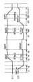
도 1은 본 발명의 제1 실시 형태에 따른 성막 방법의 시퀀스(sequence)를 나타내는 타임 차트이다.
도 2a∼도 2f는, 제1 실시 형태에 따른 시퀀스 중의 피처리체의 상태를 개략적으로 나타내는 단면도이다.
도 3은 밀착성 평가의 결과를 나타내는 도면이다.
도 4는 본 발명의 제2 실시 형태에 따른 성막 방법의 시퀀스를 나타내는 타임 차트이다.
도 5a∼도 5f는 제2 실시 형태에 따른 시퀀스 중의 피처리체의 상태를 개략적으로 나타내는 단면도이다.
도 6은 본 발명의 제3 실시 형태에 따른 성막 방법의 시퀀스를 나타내는 타임 차트이다.
도 7a∼도 7f는 제3 실시 형태에 따른 시퀀스 중의 피처리체의 상태를 개략적으로 나타내는 단면도이다.
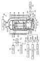
도 8은 제1∼제3 실시 형태에 따른 성막 방법을 실시하는 것이 가능한 성막 장치의 일 예를 개략적으로 나타내는 단면도이다.1 is a time chart showing a sequence of a film forming method according to the first embodiment of the present invention.
2A to 2F are cross-sectional views schematically showing the state of the object to be processed in the sequence according to the first embodiment.
It is a figure which shows the result of adhesive evaluation.
4 is a time chart showing a sequence of a film forming method according to the second embodiment of the present invention.
5A to 5F are cross-sectional views schematically showing the state of the object to be processed in the sequence according to the second embodiment.
6 is a time chart showing a sequence of a film forming method according to the third embodiment of the present invention.
7A to 7F are cross-sectional views schematically showing the state of the object to be processed in the sequence according to the third embodiment.
8 is a sectional views schematically showing an example of a film forming apparatus in which the film forming methods according to the first to third embodiments can be performed.
이하, 첨부 도면을 참조하면서 본 발명의 실시 형태에 대해서 상세하게 설명한다. 또한, 이하의 설명에 있어서, 대략 동일한 기능 및 구성을 갖는 구성 요소에 대해서는, 동일 부호를 붙이고, 중복 설명은 필요한 경우에만 행한다.EMBODIMENT OF THE INVENTION Hereinafter, embodiment of this invention is described in detail, referring an accompanying drawing. In addition, in the following description, about the component which has substantially the same function and structure, the same code | symbol is attached | subjected and duplication description is performed only when necessary.
(제1 실시 형태)(1st embodiment)
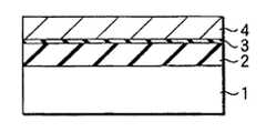
도 1은, 본 발명의 제1 실시 형태에 따른 성막 방법의 시퀀스를 나타내는 타임 차트이다. 도 2a∼도 2f는, 제1 실시 형태에 따른 시퀀스 중의 피처리체의 상태를 개략적으로 나타내는 단면도이다. 이 시퀀스는, 예를 들면, 전술한 바와 같이, 반도체 디바이스를 제조할 때의 에칭 마스크(하드 마스크)로서 사용되는 어모퍼스 카본막을 포함하는 적층 구조를 형성하는 것이다.1 is a time chart showing a sequence of a film forming method according to the first embodiment of the present invention. 2A to 2F are cross-sectional views schematically showing the state of the object to be processed in the sequence according to the first embodiment. This sequence forms a laminated structure containing an amorphous carbon film used as an etching mask (hard mask) at the time of manufacturing a semiconductor device, for example, as described above.
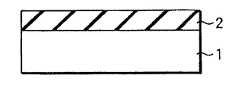
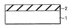
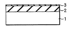
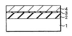
우선, 도 1 중의 공정 t1에 나타내는 바와 같이, 반도체 기판, 예를 들면, 실리콘 웨이퍼(1) 상에 두께 약 100nm의 SiO2막(2)이 형성된 피처리체(도 2a 참조)를, 성막 장치의 처리실에 반입한다. SiO2막(2)은, 나중에 어모퍼스 카본막이 형성되는 하지층이다.First, as shown in step t1 in FIG. 1, a workpiece (see FIG. 2A) in which a SiO2 film2 having a thickness of about 100 nm is formed on a semiconductor substrate, for example, a
다음으로, 공정 t2에 나타내는 바와 같이, 처리실 내부의 압력을 대기압(760Torr=1.01×10⁵Pa)으로부터 소정의 진공도, 예를 들면, 0.1Torr(13.3Pa) 미만으로 감압한다.Next, as shown in step t2, the pressure inside the processing chamber is reduced from the atmospheric pressure (760 Torr = 1.01 x 10⁵ Pa) to a predetermined degree of vacuum, for example, less than 0.1 Torr (13.3 Pa).
다음으로, 공정 t3에 나타내는 바와 같이, 처리실 내부의 압력이 안정되면, 피처리체를, 예를 들면, 약 550℃의 온도로 가열한다. 또한, 처리실 내부의 압력은, 소정의 진공도 0.1Torr 미만으로부터 0.1Torr(13.3Pa)로 올린다.Next, as shown to process t3, when the pressure in a process chamber is stabilized, a to-be-processed object will be heated to the temperature of about 550 degreeC, for example. In addition, the pressure inside a process chamber raises from predetermined | prescribed vacuum degree below 0.1 Torr to 0.1 Torr (13.3 Pa).
다음으로, 공정 t4에 나타내는 바와 같이, 처리실 내부의 압력 및, 피처리체의 온도가 안정되면, SiO2막(2)의 표면에 유기계 실리콘 가스를 공급하고, SiO2막(2)의 표면에 Si-C 결합을 포함하는 초기층(3)을 형성한다(도 2b 참조). 유기계 실리콘 가스의 예로서는, 아민계 실리콘 가스를 들 수 있다. 또한, 아민계 실리콘 가스의 예로서는, BAS(부틸아미노실란), BTBAS(비스터셔리부틸아미노실란), DMAS(디메틸아미노실란), BDMAS(비스디메틸아미노실란), TDMAS(트리디메틸아미노실란), DEAS(디에틸아미노실란), BDEAS(비스디에틸아미노실란), DPAS(디프로필아미노실란), DIPAS(디이소프로필아미노실란) 등을 들 수 있다. 본 예에서는, BTBAS를 이용한다.Next, as shown in step t4, the internal chamber pressure and, when the temperature of the subject to be treated rest, the surface of the feed an organic silicone gas to the surface of the SiO2 film 2 and, SiO2 film (2) Si Form an
본 실시 형태에 있어서, 초기층(3)을 형성하는 공정 t4의 처리 조건은 이하와 같이 설정된다.In this embodiment, the process conditions of the process t4 which forms the
BTBAS 유량 : 1∼1000sccm, 예를 들면 100sccmBTBAS flow rate: 1 to 1000 sccm, for example 100 sccm
처리 시간 : 0.1∼60min, 예를 들면 1minTreatment time: 0.1 to 60 min, for example 1 min
처리 온도 : 20∼750℃, 예를 들면 550℃Treatment temperature: 20 to 750 ° C, for example 550 ° C
처리 압력 : 0.05∼50Torr, 예를 들면 0.1Torr(13.3Pa)Treatment pressure: 0.05 to 50 Torr, for example 0.1 Torr (13.3 Pa)
다음으로, 공정 t5에 나타내는 바와 같이, 피처리체를 성막 온도로 가열함과 함께, 처리실 내부의 압력을 성막 압력까지 올린다.Next, as shown to process t5, while heating a to-be-processed object to film-forming temperature, the pressure in a process chamber is raised to film-forming pressure.
다음으로, 공정 t6에 나타내는 바와 같이, 처리실 내부의 압력 및, 피처리체의 온도가 안정되면, Si-C 결합을 포함하는 초기층(3)이 형성된 SiO2막(2) 상에, 어모퍼스 카본막(4)을 열성막한다(도 2c 참조). 어모퍼스 카본막(4)은, 탄화수소 화합물 가스를 포함하는 성막 가스를 피처리체 상에 공급하고, 탄화수소 화합물을 열분해함으로써 성막할 수 있다. 탄화수소 화합물 가스의 예로서는, CH4(메탄), C2H2(아세틸렌), C2H4(에틸렌), C2H6(에탄), C4H6(부틴) 등을 들 수 있다. 본 예에서는 C2H4를 이용한다.Next, as shown in process t6, when the pressure in a process chamber and the temperature of a to-be-processed object are stabilized, an amorphous carbon film is formed on the SiO2 film2 in which the
본 실시 형태에 있어서, 어모퍼스 카본막(4)을 형성하는 공정 t6 처리 조건은 이하와 같이 설정된다.In this embodiment, the process t6 process conditions of forming the
C2H4 유량 : 1∼5000sccm, 예를 들면 1000sccmC2 H4 Flow rate: 1 to 5000 sccm, for example 1000 sccm
성막 시간 : 0.1∼600분, 예를 들면 12.5분Deposition time: 0.1 to 600 minutes, for example 12.5 minutes
성막 온도 : 300∼1000℃, 예를 들면 800℃Film formation temperature: 300-1000 degreeC, for example 800 degreeC
성막 압력 : 1∼650Torr, 예를 들면 50Torr(6650Pa)Deposition pressure: 1 to 650 Torr, for example 50 Torr (6650 Pa)
또한, 「열성막」이란 성막 가스를 열만으로 활성화하여 피처리체 상에 막을 성막하는 성막법이며, 통상은 피처리체를 직접 혹은 간접적으로 가열한다. 이러한 성막법을, 본 명세서에 있어서는 「열성막」이라고 간략히 나타낸다.In addition, a "thermal film formation" is a film formation method which activates a film forming gas only by heat, and forms a film on a to-be-processed object, Usually, a to-be-processed object is heated directly or indirectly. Such a film formation method is briefly referred to as "thermal film formation" in the present specification.
다음으로, 공정 t7에 나타내는 바와 같이, 처리실의 내부를 배기한 후, 피처리체를 성막 온도보다도 낮은 온도로 함과 함께, 처리실 내부의 압력을 성막 압력 미만의 압력으로 한다.Next, as shown in process t7, after evacuating the inside of a process chamber, while making a to-be-processed object into temperature lower than film-forming temperature, the pressure inside a process chamber is made into the pressure below film-forming pressure.
다음으로, 공정 t8에 나타내는 바와 같이, 처리실 내부의 압력 및, 피처리체의 온도가 안정되면, 어모퍼스 카본막(4) 상에 유기계 실리콘 가스를 공급한다. 이어서 유기계 실리콘 가스를 불활성 가스(예를 들면, 질소 가스)로 퍼지(purge)한다. 이어서 도 1 중의 공정 t9에 나타내는 바와 같이 질소 함유 가스(반응 가스)를 공급한다. 이어서 질소 함유 가스를 불활성 가스(예를 들면, 질소 가스)로 퍼지한다. 그리고, 유기계 실리콘 가스의 공급(공정 t8)과, 질소 함유 가스의 공급(공정 t9)을 교대로 포함하는 상기 사이클을 반복한다.Next, as shown in process t8, when the pressure in a process chamber and the temperature of a to-be-processed object are stabilized, organic type silicon gas is supplied to the
이에 따라, 어모퍼스 카본막(4)의 표면에는, 우선, Si-C 결합을 포함하는 중간층(5)이 형성된다(도 2d 참조). 이어서 Si-C 결합을 포함하는 중간층(5)이 질화됨에 따라 어모퍼스 카본막(4) 상에 질화 실리콘을 포함하는 박막(6)이 열성막된다(도 2e 참조). 그리고, 유기계 실리콘 가스의 공급(공정 t8)과 질소 함유 가스의 공급(공정 t9)을 복수회 반복함으로써(ALD법), 소정 두께의 질화 실리콘 함유 장벽막(56)이 열성막된다. 이들 공정 t8, 공정 t9가 종료된 시점에서는, 어모퍼스 카본막(4)과 장벽막(56)과의 사이에 접착층이 되는 매우 얇은 중간층(5)이 존재하고 있는 상태가 된다. 그러나, 도면에서는 편의상, 이들 층 및 막의 두께는 정확한 것으로 되어 있지 않다.Accordingly, the
공정 t8에 있어서 이용되는 유기계 실리콘 가스의 예로서는, 아민계 실리콘 가스를 들 수 있다. 또한, 아민계 실리콘 가스의 예로서는, BAS(부틸아미노실란), BTBAS(비스터셔리부틸아미노실란), DMAS(디메틸아미노실란), BDMAS(비스디메틸아미노실란), TDMAS(트리디메틸아미노실란), DEAS(디에틸아미노실란), BDEAS(비스디에틸아미노실란), DPAS(디프로필아미노실란), DIPAS(디이소프로필아미노실란) 등을 들 수 있다. 본 예에서는, BTBAS를 이용한다.Examples of the organic silicon gas used in the step t8 include amine silicon gas. Moreover, as an example of an amine silicone gas, BAS (butylamino silane), BTBAS (bissteryl butylamino silane), DMAS (dimethylamino silane), BDMAS (bisdimethylamino silane), TDMAS (tridimethylamino silane), DEAS (Diethylaminosilane), BDEAS (bisdiethylaminosilane), DPAS (dipropylaminosilane), DIPAS (diisopropylaminosilane), etc. are mentioned. In this example, BTBAS is used.
본 실시 형태에 있어서, 중간층(5)을 형성하는 공정 t8의 처리 조건은 이하와 같이 설정된다.In this embodiment, the process conditions of the process t8 which forms the intermediate |
BTBAS 유량 : 1∼1000sccm, 예를 들면 100sccmBTBAS flow rate: 1 to 1000 sccm, for example 100 sccm
처리 시간 : 0.1∼60min, 예를 들면 5분Treatment time: 0.1 to 60 min, for example 5 minutes
처리 온도 : 20∼750℃, 예를 들면 550℃Treatment temperature: 20 to 750 ° C, for example 550 ° C
처리 압력 : 0.05∼50Torr, 예를 들면 0.1Torr(13.3Pa)Treatment pressure: 0.05 to 50 Torr, for example 0.1 Torr (13.3 Pa)
또한, 공정 t9에 있어서 이용되는 질소 함유 가스의 예로서는, NH3(암모니아)를 들 수 있다.In addition, NH3 (ammonia) is mentioned as an example of the nitrogen containing gas used at the process t9.
본 실시 형태에 있어서, 박막(6)을 형성하는 공정 t9의 처리 조건은 이하와 같이 설정된다.In this embodiment, the process conditions of the process t9 which forms the thin film 6 are set as follows.
NH3 유량 : 1∼5000sccm, 예를 들면 1000sccmNH3 flow rate: 1 to 5000 sccm, for example 1000 sccm
처리 시간 : 0.1∼60min, 예를 들면 5분Treatment time: 0.1 to 60 min, for example 5 minutes
처리 온도 : 20∼750℃, 예를 들면 550℃Treatment temperature: 20 to 750 ° C, for example 550 ° C
처리 압력 : 0.05∼750Torr, 예를 들면 1Torr(133Pa)Treatment pressure: 0.05 to 750 Torr, for example 1 Torr (133 Pa)
상기 처리 조건(예시의 값으로 특정된 것)으로 공정 t8, 공정 t9을 1사이클(반복 없음) 실시한 경우에는, 약 1nm 두께의 장벽막(56)이 형성된다. 따라서, 상기 처리 조건으로 공정 t8, 공정 t9를 3사이클(3회 반복) 실시한 경우에는 약 3nm 두께의 장벽막(56)이, 마찬가지로 5사이클(5회 반복) 실시한 경우에는 약 5nm 두께의 장벽막(56)이, 마찬가지로 10사이클(10회 반복) 실시한 경우에는 약 10nm 두께의 장벽막(56)이 형성된다.When step t8 and step t9 are performed one cycle (no repetition) under the above treatment conditions (the ones specified by the example values), the
공정 t8, t9의 소정 회수의 반복이 종료되면, 공정 t10에 나타내는 바와 같이, 피처리체의 온도를 낮추면서 처리실 내부를 배기한다. 배기가 종료되면, 공정 t11에 나타내는 바와 같이, 피처리체의 온도를 계속 낮추면서 처리실 내부에 퍼지 가스를 공급한다. 피처리체의 온도가 충분히 내려가고, 또한 처리실 내부의 압력이 대기압으로 복귀한 후, 피처리체를 처리실로부터 반출한다.When the repetition of the predetermined number of times of steps t8 and t9 is completed, as shown in step t10, the inside of the processing chamber is exhausted while lowering the temperature of the target object. When the exhaust is completed, as shown in step t11, the purge gas is supplied into the process chamber while continuously lowering the temperature of the target object. After the temperature of the workpiece is sufficiently lowered and the pressure inside the treatment chamber returns to atmospheric pressure, the workpiece is taken out of the treatment chamber.
이후, 피처리체를 다른 성막 장치의 처리실에 반입하고, 장벽막(56) 상에 적층 구조에 있어서의 어모퍼스 카본막(4)의 상부에 형성하는 상부막(7)을 형성한다. 본 예에서는 상부막(7)으로서, CVD법을 이용하여 SiO2막을 장벽막(56) 상에 형성한다(도 2f 참조).Subsequently, the object to be processed is carried into a processing chamber of another film forming apparatus, and an
이러한 제1 실시 형태에 의하면, 우선, 하지층인 SiO2막(2)의 표면에 Si-C 결합을 포함하는 초기층(3)을 형성하기 때문에, Si-C 결합을 포함하는 초기층(3)을 형성하지 않는 경우에 비교하여, 하지층과 어모퍼스 카본막(4)과의 밀착성이 향상된다는 이점을 얻을 수 있다.According to this first embodiment, since the
또한, 하지층인 SiO2막(2)의 표면에 Si-C 결합을 포함하는 초기층(3)을 형성함으로써, 어모퍼스 카본막의 표면 거칠기도 개선된다는 이점도 아울러 얻을 수 있다. 어모퍼스 카본막의 표면 거칠기가 개선되는 이유의 하나로서는, 하지층과의 밀착성이 높아짐으로써 하지층 상에 어모퍼스 카본막이 균일하게 성장하기 쉽게 되는 것에 기인한다.In addition, by forming the
또한, 제1 실시 형태에 의하면, 공정 t8, t9에 나타내는 바와 같이, 유기계 실리콘 가스의 공급(공정 t8)과, 질소 함유 가스의 공급(공정 t9)을 교대로 반복하는, 즉, ALD법을 채용한다. 이에 따라, 어모퍼스 카본막(4)의 표면에 Si-C 결합을 포함하는 중간층(5)을 형성하고, 이어서 Si-C 결합을 포함하는 중간층(5)이 표면에 형성된 어모퍼스 카본막(4) 상에 질화 실리콘 함유 장벽막(56)을 열성막한다. 이에 따라, Si-C 결합을 포함하는 중간층(5)을 형성하지 않는 경우, 혹은 장벽막(56)을 ALD법에 의해 열성막하지 않는 경우와 비교하여, 어모퍼스 카본막(4)과 상부막(7)과의 밀착성을 높일 수 있다는 이점을 얻을 수 있다. 또한, 장벽막(56)을 ALD법에 의해 열성막한 경우에는 막질이 치밀(dense)해진다. 이 때문에, 산화 장벽으로서 양호하게 기능하여, 어모퍼스 카본막(4)의 산화가 억제된다. 따라서, 장벽막(56)이 형성된 피처리체를 대기(atmosphere)에 개방한 경우에 있어서도 밀착성의 저하를 억제할 수 있다.According to the first embodiment, as shown in steps t8 and t9, the supply of the organic silicon gas (step t8) and the supply of the nitrogen-containing gas (step t9) are alternately repeated, that is, the ALD method is employed. do. Accordingly, the
도 3은, 유기계 실리콘 가스의 공급(공정 t8)과, 질소 함유 가스의 공급(공정 t9)의 반복 회수마다의 밀착성 평가의 결과를 나타내는 도면이다.3 is a diagram showing the results of the adhesion evaluation for each repetition number of supply of the organic silicon gas (step t8) and supply of the nitrogen-containing gas (step t9).
밀착성은, 상부막(7)(본 평가예에서는 SiO2막)에 접착 테이프를 접착하고 접착한 테이프를 벗겼을 때에, 상부막(7)이 박리되는지 아닌지를 평가했다.Adhesion, the
도 3에 나타내는 바와 같이, 본 평가 결과에 있어서는, 유기계 실리콘 가스의 공급(공정 t8)과, 질소 함유 가스의 공급(공정 t9)을 교대로 3회 이상 반복하면, 상부막(7)이 벗겨지지 않는다(OK)는 결과였다. 또한, 유기계 실리콘 가스의 공급(공정 t8)과, 질소 함유 가스의 공급(공정 t9)을 반복하지 않는 경우에는, 상부막(7)이 벗겨진다(NG)는 결과였다.As shown in FIG. 3, in this evaluation result, when the supply of an organic type silicon gas (step t8) and the supply of nitrogen containing gas (step t9) are repeated 3 or more times alternately, the
이와 같이, 유기계 실리콘 가스의 공급(공정 t8)과, 질소 함유 가스의 공급(공정 t9)을 교대로 반복함으로써, 반복하지 않는 경우와 비교하여 어모퍼스 카본막(4)과 이 어모퍼스 카본막(4)의 상부에 형성되는 상부막(7)과의 밀착성이 향상된다는 이점을 얻을 수 있다.Thus, by repeating the supply of the organic silicon gas (step t8) and the supply of the nitrogen-containing gas (step t9) alternately, the
(제2 실시 형태)(2nd embodiment)
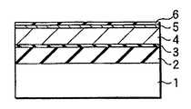
도 4는, 본 발명의 제2 실시 형태에 따른 성막 방법의 시퀀스를 나타내는 타임 차트이다. 도 5a∼도 5f는 제2 실시 형태에 따른 시퀀스 중의 피처리체의 상태를 개략적으로 나타내는 단면도이다.4 is a time chart showing a sequence of a film forming method according to the second embodiment of the present invention. 5A to 5F are cross-sectional views schematically showing the state of the object to be processed in the sequence according to the second embodiment.
또한, 도 4 및 도 5a∼도 5f에 있어서는, 도 1 및 도 2a∼도 2f와 동일 부분에는 동일한 참조 부호를 붙이고, 제1 실시 형태와 다른 부분만을 설명하기로 한다.In addition, in FIG.4 and FIG.5A-5F, the same code | symbol is attached | subjected to the same part as FIG.1 and FIG.2A-2F, and only the part different from 1st Embodiment is demonstrated.
도 4에 나타내는 바와 같이, 제2 실시 형태가 제1 실시 형태와 다른 부분은, 질소 함유 가스(반응 가스)를 공급하는 공정 t9 대신에, 탄소 함유 가스(반응 가스)를 공급하는 공정 t20을 사용하는 것이다. 탄소 함유 가스의 예로서는, 탄화수소 화합물 가스를 들 수 있다. 또한, 탄화수소 화합물 가스의 예로서는, CH4(메탄), C2H2(아세틸렌), C2H4(에틸렌), C2H6(에탄), C4H6(부틴) 등을 들 수 있다. 본 예에서는 C2H4를 이용한다.As shown in FIG. 4, the part from 2nd Embodiment different from 1st Embodiment uses the process t20 which supplies a carbon containing gas (reactive gas) instead of the process t9 which supplies a nitrogen containing gas (reactive gas). It is. Hydrocarbon compound gas is mentioned as an example of a carbon containing gas. In addition, examples of the hydrocarbon compound gas include CH4 (methane), C2 H2 (acetylene), C2 H4 (ethylene), C2 H6 (ethane), C4 H6 (butyne), and the like. . In this example, C2 H4 is used.
본 실시 형태에 있어서, 공정 t20의 처리 조건은 이하와 같이 설정된다.In this embodiment, the processing conditions of step t20 are set as follows.
C2H4 유량 : 1∼5000sccm, 예를 들면 1000sccmC2 H4 Flow rate: 1 to 5000 sccm, for example 1000 sccm
성막 시간 : 0.1∼30분, 예를 들면 0.5분Deposition time: 0.1-30 minutes, for example 0.5 minutes
성막 온도 : 20∼750℃, 예를 들면 550℃Film formation temperature: 20-750 degreeC, for example, 550 degreeC
성막 압력 : 0.05∼750Torr, 예를 들면 1Torr(133Pa)Film formation pressure: 0.05 to 750 Torr, for example 1 Torr (133 Pa)
이러한 제2 실시 형태에 있어서도, 공정 t7에 이어서 공정 t8, t20에 나타내는 바와 같이, 유기계 실리콘 가스의 공급(공정 t8)과, 탄소 함유 가스의 공급(공정 t20)을 교대로 포함하는 사이클을 반복한다. 이에 따라, 어모퍼스 카본막(4)의 표면에는, 우선, Si-C 결합을 포함하는 중간층(5)이 형성된다(도 5d 참조). 이어서 Si-C 결합을 포함하는 중간층(5)이 탄화됨으로써 어모퍼스 카본막(4) 상에 탄화 실리콘을 포함하는 박막(8)이 열성막된다(도 5e 참조). 그리고, 유기계 실리콘 가스의 공급(공정 t8)과 탄소 함유 가스의 공급(공정 t20)을 복수회 반복함으로써(ALD법), 소정 두께의 탄화 실리콘 함유 장벽막(58)이 열성막된다. 이들 공정 t8, t20이 종료된 시점에서는, 어모퍼스 카본막(4)과 장벽막(58)과의 사이에 접착층이 되는 매우 얇은 중간층(5)이 존재하고 있는 상태가 된다. 그러나, 도면에서는 편의상, 이들 층 및 막의 두께는 정확한 것으로 되어 있지 않다.Also in this 2nd Embodiment, as shown to process t8 and t20 following process t7, the cycle which alternately includes supply of organic type silicon gas (step t8) and supply of carbon containing gas (step t20) is repeated. . Accordingly, the
이에 따라, Si-C 결합을 포함하는 중간층(5)을 형성하지 않는 경우, 혹은 장벽막(58)을 ALD법에 의해 열성막하지 않는 경우와 비교하여, 어모퍼스 카본막(4)과 상부막(7)과의 밀착성을 높일 수 있다는 이점을 얻을 수 있다. 또한, 장벽막(58)은 ALD법에 의해 열성막되기 때문에, 장벽막(56)과 동일하게 막질이 치밀해진다. 이 때문에, 장벽막(58)은, 산화 장벽으로서 양호하게 기능하여 어모퍼스 카본막(4)의 산화가 억제된다. 따라서, 장벽막(58)이 형성된 피처리체를 대기에 개방한 경우에 있어서도 밀착성의 저하가 억제된다.Accordingly, the
(제3 실시 형태)(Third embodiment)
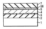
도 6은, 본 발명의 제3 실시 형태에 따른 성막 방법의 시퀀스를 나타내는 타임 차트이다. 도 7a∼도 7f는 제3 실시 형태에 따른 시퀀스 중의 피처리체의 상태를 개략적으로 나타내는 단면도이다.6 is a time chart showing a sequence of a film forming method according to the third embodiment of the present invention. 7A to 7F are cross-sectional views schematically showing the state of the object to be processed in the sequence according to the third embodiment.
또한, 도 6 및 도 7a∼도 7f에 있어서는, 도 1 및 도 2a∼도 2f와 동일 부분에는 동일한 참조 부호를 붙이고, 제1 실시 형태와 다른 부분만을 설명하기로 한다.In addition, in FIG.6 and FIG.7A-7F, the same code | symbol is attached | subjected to the same part as FIG.1 and FIG.2A-2F, and only the part different from 1st Embodiment is demonstrated.
도 6에 나타내는 바와 같이, 제3 실시 형태가 제1 실시 형태와 다른 부분은, 공정 t8, t9 대신에 어모퍼스 카본막(4) 상에 유기계 실리콘 가스를 공급하는 공정 t30과, 다음으로 유기계 실리콘 가스를 정지한 상태에서 어닐 처리를 행하는 공정 t32를 사용하는 것에 있다.As shown in FIG. 6, the third embodiment differs from the first embodiment in the step t30 of supplying the organic silicon gas on the
이러한 제3 실시 형태에 있어서도, 공정 t7에 이어서 공정 t30에 나타내는 바와 같이, 유기계 실리콘 가스를 공급하고, 어모퍼스 카본막(4)의 표면에 Si-C 결합을 포함하는 중간층(5)을 형성한다(도 7d 참조). 또한, 이 공정은 어느 정도의 길이로 함으로써, Si-C 결합을 포함하는 중간층(5) 및 그 위에 추가로 탄화 실리콘 함유막(9)을 열성막하는 공정(도 7e 참조)으로 해석할 수 있다.Also in this 3rd Embodiment, as shown to process t30 following process t7, organic type silicon gas is supplied and the intermediate |
공정 t30에 있어서 이용되는 유기계 실리콘 가스의 예로서는, 아민계 실리콘 가스를 들 수 있다. 또한, 아민계 실리콘 가스의 예로서는, BAS(부틸아미노실란), BTBAS(비스터셔리부틸아미노실란), DMAS(디메틸아미노실란), BDMAS(비스디메틸아미노실란), TDMAS(트리디메틸아미노실란), DEAS(디에틸아미노실란), BDEAS(비스디에틸아미노실란), DPAS(디프로필아미노실란), DIPAS(디이소프로필아미노실란) 등을 들 수 있다. 본 예에서는 BTBAS를 이용한다.Examples of the organic silicon gas used in the step t30 include an amine silicon gas. Moreover, as an example of an amine silicone gas, BAS (butylamino silane), BTBAS (bissteryl butylamino silane), DMAS (dimethylamino silane), BDMAS (bisdimethylamino silane), TDMAS (tridimethylamino silane), DEAS (Diethylaminosilane), BDEAS (bisdiethylaminosilane), DPAS (dipropylaminosilane), DIPAS (diisopropylaminosilane), etc. are mentioned. In this example, BTBAS is used.
본 실시 형태에 있어서, 공정 t30의 처리 조건은 이하와 같이 설정된다.In this embodiment, the processing conditions of step t30 are set as follows.
BTBAS 유량 : 1∼1000sccm, 예를 들면 100sccmBTBAS flow rate: 1 to 1000 sccm, for example 100 sccm
처리 시간 : 0.1∼60분, 예를 들면 5분Treatment time: 0.1 to 60 minutes, for example 5 minutes
처리 온도 : 20∼750℃, 예를 들면 550℃Treatment temperature: 20 to 750 ° C, for example 550 ° C
처리 압력 : 0.05∼50Torr, 예를 들면 0.1Torr(13.3Pa)Treatment pressure: 0.05 to 50 Torr, for example 0.1 Torr (13.3 Pa)
공정 t30에서 어모퍼스 카본막(4) 상에 Si-C 결합을 포함하는 중간층(5) 및 탄화 실리콘 함유막(9)을 형성한 후, 처리실의 내부를 배기한다. 이어서 공정 t31에 나타내는 바와 같이, 처리실 내부의 압력을 공정 t30보다 높은 압력으로 올린다. 또한, 피처리체의 온도를 공정 t30보다 높은 온도로 올린다.After forming the intermediate |
이어서, 공정 t32에 나타내는 바와 같이, 처리실 내부의 압력 및, 피처리체의 온도가 안정되면, 처리실 내에 불활성 가스를 공급하면서 피처리체를 불활성 가스 분위기 하에서 어닐 처리한다. 공정 t32에 있어서 이용되는 불활성 가스의 예로서는, 질소 가스를 들 수 있다.Subsequently, as shown in step t32, when the pressure inside the processing chamber and the temperature of the processing target are stabilized, the processing target is annealed under an inert gas atmosphere while supplying an inert gas into the processing chamber. Nitrogen gas is mentioned as an example of the inert gas used at the process t32.
본 실시 형태에 있어서, 공정 t32의 처리 조건은 이하와 같이 설정된다.In this embodiment, the processing conditions of step t32 are set as follows.
N2 유량 : 50∼30000sccm, 예를 들면 1000sccmN2 flow rate: 50 to 30000 sccm, for example 1000 sccm
처리 시간 : 0.5∼300분, 예를 들면 30분Treatment time: 0.5 to 300 minutes, for example 30 minutes
처리 온도 : 550∼1200℃, 예를 들면 800℃Treatment temperature: 550 to 1200 ° C, for example 800 ° C
처리 압력 : 0.1∼760Torr, 예를 들면 400Torr(53200Pa)Treatment pressure: 0.1 to 760 Torr, for example 400 Torr (53200 Pa)
이러한 제3 실시 형태에 있어서도, 어모퍼스 카본막(4)의 표면에 Si-C 결합을 포함하는 중간층(5)을 형성하고, 다음으로 탄화 실리콘 함유막(9)을 열성막한다. 또한, 탄화 실리콘 함유막(9)을, 이 탄화 실리콘 함유막(9)을 열성막했을 때보다 높은 압력 및 높은 온도로 불활성 가스 분위기 하에서 어닐 처리한다.Also in this 3rd embodiment, the intermediate |
이에 따라, Si-C 결합을 포함하는 중간층(5)을 형성하지 않는 경우, 혹은 탄화 실리콘 함유막(9)을 어닐 처리하지 않는 경우와 비교하여, 어모퍼스 카본막(4)과 상부막(7)과의 밀착성을 높일 수 있다는 이점을 얻을 수 있다.Accordingly, the
또한, 탄화 실리콘 함유막(9)은 어닐 처리되기 때문에, 장벽막(56)과 동일하게 막질이 치밀해진다. 이 때문에, 탄화 실리콘 함유막(9)은, 산화 장벽으로서 양호하게 기능하여 어모퍼스 카본막(4)의 산화가 억제된다. 따라서, 탄화 실리콘 함유막(9)이 형성된 피처리체를 대기에 개방한 경우에 있어서도 밀착성의 저하가 억제된다.In addition, since the silicon
(제4 실시 형태)(4th embodiment)
제4 실시 형태는, 상기 제1∼제3 실시 형태에 따른 성막 방법을 실시하는 것이 가능한 성막 장치의 일 예에 관한 것이다.4th Embodiment is related with an example of the film-forming apparatus which can implement the film-forming method which concerns on said 1st-3rd embodiment.
도 8은, 제1∼제3 실시 형태에 따른 성막 방법을 실시하는 것이 가능한 성막 장치의 일 예를 개략적으로 나타내는 단면도이다.FIG. 8: is sectional drawing which shows schematically an example of the film-forming apparatus which can implement the film-forming method which concerns on 1st-3rd embodiment.
도 8에 나타내는 바와 같이, 성막 장치(100)는, 하단이 개구된 천정이 있는 원통체 형상의 처리실(101)을 갖고 있다. 처리실(101)의 전체는, 예를 들면, 석영에 의해 형성되어 있다. 처리실(101) 내의 천정에는, 석영제의 천정판(102)이 설치되어 있다. 처리실(101)의 하단 개구부에는, 예를 들면, 스테인리스 스틸에 의해 원통체 형상으로 성형된 매니폴드(manifold; 103)가 O링 등의 시일 부재(104)를 개재하여 연결되어 있다.As shown in FIG. 8, the film-forming
매니폴드(103)는 처리실(101)의 하단을 지지하고 있다. 매니폴드(103)의 하단 개구로부터는 피처리체로서 복수매, 예를 들면, 50∼100매의 반도체 기판, 본 예에서는, 실리콘 웨이퍼(1)를 다단으로 재치 가능한 석영제의 웨이퍼 보트(105)가 처리실(101) 내에 삽입 가능하게 되어 있다. 본 예에서는, 각 실리콘 웨이퍼(1) 상에, 예를 들면 SiO2막이 배설되고, 이것은 전술한 바와 같이 어모퍼스 카본막을 포함하는 적층 구조가 그 위에 형성되게 하는 하지층으로서 기능한다. 웨이퍼 보트(105)는 복수개의 지주(106)를 갖고, 지주(106)에 형성된 홈에 의해 복수매의 실리콘 웨이퍼(1)가 지지되게 되어 있다.The manifold 103 supports the lower end of the
웨이퍼 보트(105)는, 석영제의 보온통(107)을 개재하여 테이블(108) 상에 올려놓여져 있다. 테이블(108)은, 매니폴드(103)의 하단 개구부를 개폐하는, 예를 들면, 스테인리스 스틸제의 덮개부(109)를 관통하는 회전축(110) 상에 지지된다. 회전축(110)의 관통부에는, 예를 들면, 자성 유체 시일(111)이 설치되고, 회전축(110)을 기밀하게 시일하면서 회전 가능하게 지지하고 있다. 덮개부(109)의 주변부와 매니폴드(103)의 하단부와의 사이에는, 예를 들면, O링으로 이루어지는 시일 부재(112)가 개설(interpose)되어 있다. 이에 따라 처리실(101) 내의 시일성이 보지(保持; holding)되어 있다. 회전축(110)은, 예를 들면, 보트 엘리베이터(boat elevator) 등의 승강 기구(도시하지 않음)에 지지된 아암(arm; 113)의 선단에 부착되어 있다. 승강 기구에 의해 웨이퍼 보트(105)가 덮개부(109)를 개재하여 승강되어, 처리실(101) 내에 대하여 삽입·이탈된다.The
성막 장치(100)는, 처리실(101) 내에 처리에 사용하는 가스를 공급하는 처리 가스 공급 기구(114)와, 처리실(101) 내에 퍼지 가스를 공급하는 퍼지 가스 공급 기구(115)를 갖고 있다.The film-forming
처리 가스 공급 기구(114)는 유기계 실리콘 가스 공급원(117), 탄화수소 화합물 가스 공급원(118), 질소 함유 가스 공급원(119)을 포함하고 있다. 퍼지 가스 공급 기구(115)는 불활성 가스 공급원(120)을 포함하고 있다.The processing
유기계 실리콘 가스 공급원(117)은 유량 제어기(121a) 및 개폐 밸브(122a)를 개재하여, 분산 노즐(123)에 접속되어 있다. 분산 노즐(123)은 석영관으로 이루어지며, 매니폴드(103)의 측벽을 내측으로 관통하여 상방향으로 굴곡되어 수직으로 연장된다. 분산 노즐(123)의 수직 부분에는, 웨이퍼 보트(105)의 웨이퍼 지지 범위에 대응하는 상하 방향의 길이에 걸쳐 복수의 가스 토출공(124)이 소정의 간격을 두고 형성되어 있다. 유기계 실리콘 가스는, 각 가스 토출공(124)으로부터 수평 방향으로 처리실(101) 내를 향하여 대략 균일하게 토출된다.The organic silicon
탄화수소 화합물 가스 공급원(118)은 유량 제어기(121b) 및 개폐 밸브(122b)를 개재하여, 분산 노즐(125)에 접속되어 있다. 질소 함유 가스 공급원(119)도 또한, 유량 제어기(121c) 및 개폐 밸브(122c)를 개재하여, 분산 노즐(125)에 접속되어 있다. 분산 노즐(125)은 석영관으로 이루어지며, 매니폴드(103)의 측벽을 내측으로 관통하여 상방향으로 굴곡되어 수직으로 연장된다. 분산 노즐(125)의 수직 부분에는, 웨이퍼 보트(105)의 웨이퍼 지지 범위에 대응하는 상하 방향의 길이에 걸쳐 복수의 가스 토출공(126)이 소정의 간격을 두고 형성되어 있다. 탄화수소 화합물 가스, 또는 질소 함유 가스는 각 가스 토출공(126)으로부터 수평 방향으로 처리실(101) 내를 향하여 대략 균일하게 토출된다.The hydrocarbon compound
퍼지 가스 공급 기구(115)는 불활성 가스 공급원(120)을 포함하고 있다. 불활성 가스 공급원(120)은 유량 제어기(121d) 및 개폐 밸브(122d)를 개재하여, 짧은 노즐(128)에 접속되어 있다. 노즐(128)은 석영관으로 이루어지며, 매니폴드(103)의 측벽을 관통하여, 그의 선단으로부터 불활성 가스를 수평 방향으로 처리실(101) 내를 향하여 토출시킨다.The purge
처리실(101) 내의, 분산 노즐(123 및 125)과 반대측 부분에는, 처리실(101) 내를 배기하기 위한 배기구(129)가 설치되어 있다. 배기구(129)는 처리실(101)의 측벽을 상하 방향으로 깎아냄으로써 가늘고 길게 형성되어 있다. 처리실(101)의 배기구(129)에 대응하는 부분에는, 배기구(129)를 덮도록 단면이 ㄷ자 형상으로 성형된 배기구 커버 부재(130)가 용접에 의해 부착되어 있다. 배기구 커버 부재(130)는 처리실(101)의 측벽을 따라 상방으로 연장되어 있고, 처리실(101)의 상방에 가스 출구(131)를 규정하고 있다. 가스 출구(131)에는 진공 펌프 등을 포함하는 배기 기구(132)가 접속된다. 배기 기구(132)는 처리실(101) 내를 배기함으로써 처리에 사용한 처리 가스의 배기 및, 처리실(101) 내의 압력을 처리에 따른 처리 압력으로 한다.An
처리실(101)의 외주에는 통체 형상의(cylindrical) 가열 기구(133)가 설치되어 있다. 가열 기구(133)는 처리실(101) 내에 공급된 가스를 활성화시킴과 함께, 처리실(101) 내에 수용된 피처리체, 예를 들면, 반도체 기판, 본 예에서는 실리콘 웨이퍼(1)를 가열한다.A
성막 장치(100) 각부의 제어는, 예를 들면 마이크로 프로세서(컴퓨터)로 이루어지는 컨트롤러(150)에 의해 행해진다. 컨트롤러(150)에는 오퍼레이터가 성막 장치(100)를 관리하기 위해 커맨드의 입력 조작 등을 행하는 키보드나, 성막 장치(100)의 가동 상황을 가시화하여 표시하는 디스플레이 등으로 이루어지는 유저 인터페이스(151)가 접속되어 있다.Control of each part of the film-forming
컨트롤러(150)에는 기억부(152)가 접속되어 있다. 기억부(152)는 성막 장치(100)에서 실행되는 각종 처리를 컨트롤러(150)의 제어로 실현하기 위한 제어 프로그램이나, 처리 조건에 따라서 성막 장치(100)의 각 구성부에 처리를 실행시키기 위한 프로그램, 즉 레시피가 격납된다. 레시피는, 예를 들면 기억부(152) 속의 기억 매체에 기억된다. 기억 매체는 하드 디스크나 반도체 메모리 등의 고정형(stationary type)의 것이라도 좋고, CD-ROM, DVD, 플래시 메모리 등의 가반성(portable type)의 것이라도 좋다. 또한, 다른 장치로부터, 예를 들면 전용 회선을 개재하여 레시피를 적절히 전송시키도록 해도 좋다. 레시피는, 필요에 따라서, 유저 인터페이스(151)로부터의 지시 등으로 기억부(152)로부터 읽혀지고, 읽어낸 레시피에 따른 처리를 컨트롤러(150)가 실행함으로써, 성막 장치(100)는 컨트롤러(150)의 제어 아래, 원하는 처리가 실시된다.The
본 예에서는, 컨트롤러(150)의 제어 아래, 상기 제1∼제3 실시 형태에 따른 성막 방법 중, 상부막(7)의 성막을 위한 부분을 제외한 도 1에 나타낸 공정 t1∼공정 t11에 따른 처리, 또는 도 4에 나타낸 공정 t1∼t8, t20, t10∼t11에 따른 처리, 또는 도 6에 나타낸 공정 t1∼t7, t30∼t32, t10+t11에 따른 처리가 순차로 실시된다.In this example, under the control of the
전술한 바와 같이, 상기 제1∼제3 실시 형태에 따른 성막 방법은, 도 8에 나타내는 바와 같은 성막 장치(100)를 이용하여 실시할 수 있다. 게다가, 성막 장치(100)에 의하면, 제1∼제3 실시 형태에 따른 성막 방법의 각 처리를, 상부막(7)의 성막을 위한 부분을 제외하고, 대기에 개방하는 일 없이 동일한 처리실(101) 내에서 연속하여 행할 수 있다.As mentioned above, the film-forming method which concerns on said 1st-3rd embodiment can be implemented using the film-forming
또한, 성막 장치(100)는 질소 함유 가스 공급원(119)을 구비하고 있지만, 제2, 제3 실시 형태를 실시하는 경우에는 질소 함유 가스 공급원(119)을 생략할 수도 있다. 질소 함유 가스 공급원(119)을 생략한 경우, 예를 들면, 제2 실시 형태에 있어서의 공정 t20에 대해서는, 탄화수소 화합물 가스 공급원(118)으로부터 탄소 함유 가스를 공급하면 좋다.In addition, although the film-forming
이상, 본 발명을 몇 가지 실시 형태에 따라 설명했지만, 본 발명은 상기 몇 가지 실시 형태에 한정되는 것은 아니고, 여러 가지 변형이 가능하다.As mentioned above, although this invention was demonstrated according to some embodiment, this invention is not limited to said some embodiment, A various deformation | transformation is possible.
예를 들면, 어모퍼스 카본막과 하지층과의 밀착성 및, 어모퍼스 카본막과 상부막과의 밀착성은, 쌍방을 동시에 향상시키는 것이 바람직하지만, 어느 한쪽만을 개선하도록 해도 좋다. 예를 들면, 상부막을 형성하지 않는 경우에는, 공정 t1∼공정 t6까지를 행하여 어모퍼스 카본막과 하지층과의 밀착성만을 향상시켜도 좋다.For example, the adhesion between the amorphous carbon film and the underlying layer and the adhesion between the amorphous carbon film and the upper film are preferably improved at the same time, but only one of them may be improved. For example, when the upper film is not formed, only the adhesion between the amorphous carbon film and the underlying layer may be performed by performing steps t1 to t6.
또한, 상기 몇 가지 실시 형태에 있어서는, 평탄한 하지층 상에 어모퍼스 카본막을 성막하는 예 및, 평탄한 어모퍼스 카본막 상에 상부막을 성막하는 예를 나타냈다. 그러나, 상기 몇 가지의 실시 형태 모두가 열성막 프로세스이고, 열성막 프로세스는 스텝 커버리지(step coverage)가 우수한 것이다. 이 때문에, 단차를 갖는 하지층 상에 어모퍼스 카본막을 성막하는 경우 및, 단차를 갖는 어모퍼스 카본막 상에 상부막을 성막하는 경우에도 문제는 발생하지 않는다.In some of the above embodiments, an example in which an amorphous carbon film is formed on a flat base layer and an example in which an upper film is formed on a flat amorphous carbon film are shown. However, all of the above described embodiments are thermal film forming processes, and the thermal film forming process is excellent in step coverage. For this reason, a problem does not arise even when an amorphous carbon film is formed into a film on a base layer which has a step difference, and when an upper film is formed into a film of an amorphous carbon film which has a step difference.
또한, 상기 몇 가지 실시 형태에 있어서는, 하지층 및 상부막의 쌍방을 SiO2로 했지만, 하지층 및 상부막은 SiO2에 한정되는 것도 아니다. 예를 들면, 하지층 및 상부막의 각각은 실리콘을 함유하는 다른 재료라도 좋고, 이 경우도 어모퍼스 카본막과 하지층 혹은 어모퍼스 카본막과 상부막과의 사이에 Si-C 결합을 발생시킬 수 있다.Furthermore, nor is it to be in the above-mentioned several embodiments, but the base layer and the upper layer both as SiO2, only the base layer and the top film is SiO2. For example, each of the base layer and the top film may be another material containing silicon, and in this case, Si-C bonds can be generated between the amorphous carbon film and the base layer or the amorphous carbon film and the top film.
또한, 상기 몇 가지 실시 형태에 있어서는, 본 발명은 배치식(batch type)의 성막 장치에 적용되지만, 이를 대신하여 본 발명은 매엽식(single-substrate type)의 성막 장치에 적용 가능하다.In addition, in some of said embodiments, this invention is applied to the film-forming apparatus of a batch type, but instead this invention is applicable to the film-forming apparatus of a single-substrate type.
또한, 상기 몇 가지 실시 형태에 있어서는, 처리 조건을 구체적으로 나타냈지만, 이들은 단순한 예이며, 그것은 다음과 같은 이유에 의한다.In addition, although the processing conditions were shown concretely in the said some embodiment, these are simple examples and it is for the following reasons.
본 발명에 의한 제1 이점인 하지층과 어모퍼스 카본막(4)과의 밀착성 향상은, 하지층의 표면에 Si-C 결합을 포함하는 초기층(3)을 형성하고, 그 위에 어모퍼스 카본막(4)을 열성막함으로써 얻어진다.The adhesiveness improvement of the base layer and the
본 발명에 의한 제2 이점인 어모퍼스 카본막(4)과 상부막(7)과의 밀착성 향상은, 어모퍼스 카본막(4)의 표면에 Si-C 결합을 포함하는 중간층(5)을 형성하고, 그 위에 장벽막(56 또는 58)을 유기계 실리콘 가스의 공급(공정 t8)과, 질소 함유 가스의 공급(공정 t9) 또는 탄소 함유 가스 공급(t20)을 교대로 반복하는, 즉, ALD법에 의해 열성막함으로써 얻어진다.Adhesion improvement of the
대신에, 본 발명에 의한 제2 이점인 어모퍼스 카본막(4)과 상부막(7)과의 밀착성 향상은, 어모퍼스 카본막(4)의 표면에 Si-C 결합을 포함하는 중간층(5)을 형성하고, 그 위에 탄화 실리콘 함유막(9)을 열성막하고, 또한, 탄화 실리콘 함유막(9)을, 이 탄화 실리콘 함유막(9)을 열성막했을 때보다 높은 압력 및 높은 온도로 불활성 가스 분위기 하에서 어닐 처리함으로써 얻어진다.Instead, the improvement of the adhesion between the
따라서, 상기 실시 형태에 기재한 구체적인 처리 조건은 단순한 예시이며, 실리콘 웨이퍼(1)의 크기, 처리실의 용적 변화 등에 따라서 상기 이점을 손상시키지 않는 범위에서 변경할 수 있다.Therefore, the specific processing conditions described in the above embodiments are merely examples and can be changed within a range that does not impair the above advantages depending on the size of the
또한, 상기 실시 형태에 기재한 성막 방법에 의하면, 나노미터(nm) 오더의 막두께 치수로 성막되는 것이기 때문에, 반도체 디바이스의 제조 프로세스에 매우 적합하게 이용할 수 있다. 또한, 상기 실시 형태에 기재한 성막 방법이 이용된 어모퍼스 카본막은 하지층과의 밀착성 및, 상부막과의 밀착성이 높다. 이 때문에, 각 실시 형태의 어모퍼스 카본막을 포함하는 적층 구조는, 반도체 디바이스의 제조 프로세스에 있어서, 예를 들면, 에칭 마스크로서 사용되는 하드 마스크에 특히 매우 적합하게 이용할 수 있다.Moreover, according to the film-forming method described in the said embodiment, since it forms into a film thickness dimension of a nanometer (nm) order, it can use suitably for the manufacturing process of a semiconductor device. Moreover, the amorphous carbon film using the film-forming method described in the said embodiment has high adhesiveness with a base layer, and adhesiveness with an upper film. For this reason, the laminated structure containing the amorphous carbon film of each embodiment can be used especially suitably for the hard mask used as an etching mask in the manufacturing process of a semiconductor device, for example.
Claims (21)
Translated fromKorean상기 하지층의 표면에 Si-C 결합을 포함하는 초기층을 형성하는 공정과, 여기에서 상기 하지층 상에 유기계 실리콘 가스를 공급하는 것과,
상기 초기층이 표면에 형성된 상기 하지층 상에 상기 어모퍼스 카본막을 열성막(熱成膜)으로 형성하는 공정과, 여기에서 상기 하지층 상에 탄화수소 화합물 가스를 포함하는 성막 가스를 공급하는 것을 구비하는, 어모퍼스 카본막을 포함하는 적층 구조를 하지층 상에 형성하는 방법.As a method of forming a laminated structure containing an amorphous carbon film on a base layer,
Forming an initial layer including a Si—C bond on the surface of the underlayer, supplying an organic silicon gas onto the underlayer,
Forming the amorphous carbon film as a thermal film on the base layer having the initial layer formed on the surface, and supplying a film forming gas containing a hydrocarbon compound gas to the base layer. And forming a laminated structure containing an amorphous carbon film on a base layer.
상기 하지층은 실리콘을 포함하는 층인, 어모퍼스 카본막을 포함하는 적층 구조를 하지층 상에 형성하는 방법.The method of claim 1,
And the base layer is a layer containing silicon, forming a laminated structure comprising an amorphous carbon film on the base layer.
상기 하지층은 SiO2층인, 어모퍼스 카본막을 포함하는 적층 구조를 하지층 상에 형성하는 방법.The method of claim 1,
The base layer is a method of forming a laminated structure comprising an amorphous carbon film, the SiO2 layer on the base layer.
상기 유기계 실리콘 가스는 아민계 실리콘 가스인, 어모퍼스 카본막을 포함하는 적층 구조를 하지층 상에 형성하는 방법.The method of claim 1,
And the organic silicon gas is an amine silicon gas, forming a laminated structure comprising an amorphous carbon film on the underlying layer.
상기 아민계 실리콘 가스는 부틸아미노실란, 비스터셔리부틸아미노실란, 디메틸아미노실란, 비스디메틸아미노실란, 트리디메틸아미노실란, 디에틸아미노실란, 비스디에틸아미노실란, 디프로필아미노실란, 디이소프로필아미노실란으로 이루어지는 군으로부터 선택되는, 어모퍼스 카본막을 포함하는 적층 구조를 하지층 상에 형성하는 방법.The method of claim 4, wherein
The amine-based silicone gas is butylamino silane, bisterary butyl amino silane, dimethyl amino silane, bis dimethyl amino silane, tri dimethyl amino silane, diethyl amino silane, bis diethyl amino silane, dipropyl amino silane, diisopropyl A method for forming a laminated structure comprising an amorphous carbon film, selected from the group consisting of aminosilanes, on an underlying layer.
상기 탄화수소 화합물 가스는 CH4, C2H2, C2H4, C2H6, C4H6으로 이루어지는 군으로부터 선택되는, 어모퍼스 카본막을 포함하는 적층 구조를 하지층 상에 형성하는 방법.The method of claim 1,
The hydrocarbon compound gas is a method of forming a laminated structure comprising an amorphous carbon film, selected from the group consisting of CH4 , C2 H2 , C2 H4 , C2 H6 , C4 H6 , on an underlying layer.
상기 초기층을 형성하는 공정은 처리 온도 20∼750℃와 처리 압력 0.05∼50Torr를 사용하고, 상기 어모퍼스 카본막을 형성하는 공정은 처리 온도 300∼1000℃와 처리 압력 1∼650Torr를 사용하는, 어모퍼스 카본막을 포함하는 적층 구조를 하지층 상에 형성하는 방법.The method of claim 1,
The process of forming the said initial layer uses the processing temperature of 20-750 degreeC, and the processing pressure of 0.05-50 Torr, The process of forming the amorphous carbon film uses the process carbon of 300-1000 degreeC and the processing pressure of 1-650 Torr A method of forming a laminated structure comprising a film on an underlayer.
상기 어모퍼스 카본막을 형성하는 공정 후에, 상기 방법은 추가로,
상기 어모퍼스 카본막의 표면에 Si-C 결합을 포함하는 중간층을 형성하는 공정과, 여기에서 상기 어모퍼스 카본막 상에 상기 유기계 실리콘 가스를 공급하는 것과,
상기 중간층이 표면에 형성된 상기 어모퍼스 카본막 상에 소정 두께의 질화 실리콘을 포함하는 장벽막을 열성막으로 형성하는 공정과, 여기에서 상기 어모퍼스 카본막 상에 질소를 포함하는 반응 가스를 공급하는 것 및 상기 유기계 실리콘 가스를 공급하는 것을 교대로 복수회 반복하는 것과,
상기 장벽막 상에, 상기 적층 구조에 있어서 상기 어모퍼스 카본막의 상방에 배치되는 실리콘을 포함하는 상부막을 형성하는 공정을 구비하는, 어모퍼스 카본막을 포함하는 적층 구조를 하지층 상에 형성하는 방법.The method of claim 1,
After the step of forming the amorphous carbon film, the method further comprises:
Forming an intermediate layer containing a Si—C bond on the surface of the amorphous carbon film, supplying the organic silicon gas onto the amorphous carbon film,
Forming a barrier film containing silicon nitride having a predetermined thickness as a thermal film on the amorphous carbon film having the intermediate layer formed on the surface thereof, supplying a reaction gas containing nitrogen on the amorphous carbon film, and the Alternately repeating the supply of the organic silicon gas a plurality of times,
A method of forming a laminated structure comprising an amorphous carbon film on a base layer, the method comprising: forming an upper film containing silicon disposed above the amorphous carbon film in the laminated structure on the barrier film.
상기 상부막은 SiO2막인, 어모퍼스 카본막을 포함하는 적층 구조를 하지층 상에 형성하는 방법.The method of claim 8,
And wherein the upper film is a SiO2 film, and forms a laminated structure comprising an amorphous carbon film on the underlying layer.
상기 반응 가스는 NH3 가스인, 어모퍼스 카본막을 포함하는 적층 구조를 하지층 상에 형성하는 방법.The method of claim 8,
And the reactive gas is an NH3 gas, forming a laminated structure comprising an amorphous carbon film on the underlying layer.
상기 상부막은 CVD로 형성하는, 어모퍼스 카본막을 포함하는 적층 구조를 하지층 상에 형성하는 방법.The method of claim 8,
And the upper film is formed by a CVD, the laminated structure comprising an amorphous carbon film on a base layer.
상기 중간층을 형성하는 공정 및 상기 장벽막을 형성하는 공정에 있어서, 상기 유기계 실리콘 가스를 공급하는 것은 처리 온도 20∼750℃와 처리 압력 0.05∼50Torr로 행하고, 상기 반응 가스를 공급하는 것은 처리 온도 20∼750℃와 처리 압력 0.05∼750Torr로 행하는, 어모퍼스 카본막을 포함하는 적층 구조를 하지층 상에 형성하는 방법.The method of claim 8,
In the step of forming the intermediate layer and the step of forming the barrier film, the supplying of the organic silicon gas is performed at a processing temperature of 20 to 750 ° C. and a processing pressure of 0.05 to 50 Torr. The method of forming the laminated structure containing an amorphous carbon film on 750 degreeC and processing pressure 0.05-750 Torr on a base layer.
상기 어모퍼스 카본막을 형성하는 공정 후에, 상기 방법은 추가로,
상기 어모퍼스 카본막의 표면에 Si-C 결합을 포함하는 중간층을 형성하는 공정과, 여기에서 상기 어모퍼스 카본막 상에 상기 유기계 실리콘 가스를 공급하는 것과,
상기 중간층이 표면에 형성된 상기 어모퍼스 카본막 상에 소정 두께의 탄화 실리콘을 포함하는 장벽막을 열성막으로 형성하는 공정과, 여기에서 상기 어모퍼스 카본막 상에 탄소를 포함하는 반응 가스를 공급하는 것 및 상기 유기계 실리콘 가스를 공급하는 것을 교대로 복수회 반복하는 것과,
상기 장벽막 상에, 상기 적층 구조에 있어서 상기 어모퍼스 카본막의 상방에 배치되는 실리콘을 포함하는 상부막을 형성하는 공정을 구비하는, 어모퍼스 카본막을 포함하는 적층 구조를 하지층 상에 형성하는 방법.The method of claim 1,
After the step of forming the amorphous carbon film, the method further comprises:
Forming an intermediate layer containing a Si—C bond on the surface of the amorphous carbon film, supplying the organic silicon gas onto the amorphous carbon film,
Forming a barrier film containing silicon carbide having a predetermined thickness as a thermal film on the amorphous carbon film having the intermediate layer formed on a surface thereof, and supplying a reaction gas containing carbon on the amorphous carbon film, and the Alternately repeating the supply of the organic silicon gas a plurality of times,
A method of forming a laminated structure comprising an amorphous carbon film on a base layer, the method comprising: forming an upper film containing silicon disposed above the amorphous carbon film in the laminated structure on the barrier film.
상기 상부막은 SiO2막인, 어모퍼스 카본막을 포함하는 적층 구조를 하지층 상에 형성하는 방법.The method of claim 13,
And wherein the upper film is a SiO2 film, and forms a laminated structure comprising an amorphous carbon film on the underlying layer.
상기 반응 가스는 CH4, C2H2, C2H4, C2H6, C4H6으로 이루어지는 군으로부터 선택되는, 어모퍼스 카본막을 포함하는 적층 구조를 하지층 상에 형성하는 방법.The method of claim 13,
And the reaction gas is selected from the group consisting of CH4 , C2 H2 , C2 H4 , C2 H6 , and C4 H6 , forming a laminated structure comprising an amorphous carbon film on the underlying layer.
상기 상부막은 CVD로 형성하는, 어모퍼스 카본막을 포함하는 적층 구조를 하지층 상에 형성하는 방법.The method of claim 13,
And the upper film is formed by a CVD, the laminated structure comprising an amorphous carbon film on a base layer.
상기 중간층을 형성하는 공정 및 상기 장벽막을 형성하는 공정에 있어서, 상기 유기계 실리콘 가스를 공급하는 것은 처리 온도 20∼750℃와 처리 압력 0.05∼50Torr로 행하고, 상기 반응 가스를 공급하는 것은 처리 온도 20∼750℃와 처리 압력 0.05∼750Torr로 행하는, 어모퍼스 카본막을 포함하는 적층 구조를 하지층 상에 형성하는 방법.The method of claim 13,
In the step of forming the intermediate layer and the step of forming the barrier film, the supplying of the organic silicon gas is performed at a processing temperature of 20 to 750 ° C. and a processing pressure of 0.05 to 50 Torr. The method of forming the laminated structure containing an amorphous carbon film on 750 degreeC and processing pressure 0.05-750 Torr on a base layer.
상기 어모퍼스 카본막을 형성하는 공정 후에, 상기 방법은 추가로,
상기 어모퍼스 카본막의 표면에 Si-C 결합을 포함하는 중간층을 형성함과 함께 탄화 실리콘 함유막을 열성막으로 형성하는 공정과, 여기에서 상기 어모퍼스 카본막 상에 상기 유기계 실리콘 가스를 공급하는 것과,
상기 탄화 실리콘 함유막에 대하여 불활성 가스 분위기 하에서 어닐 처리하는 공정과, 여기에서 상기 탄화 실리콘 함유막을 형성했을 때의 온도 및 압력보다도 모두 높은 온도 및 압력을 사용하는 것과,
상기 어닐 처리 후의 상기 탄화 실리콘 함유막 상에, 상기 적층 구조에 있어서 상기 어모퍼스 카본막의 상방에 배치되는 실리콘을 포함하는 상부막을 형성하는 공정을 구비하는, 어모퍼스 카본막을 포함하는 적층 구조를 하지층 상에 형성하는 방법.The method of claim 1,
After the step of forming the amorphous carbon film, the method further comprises:
Forming an intermediate layer containing Si—C bonds on the surface of the amorphous carbon film and forming a silicon carbide-containing film as a thermal film, wherein the organic silicon gas is supplied onto the amorphous carbon film;
Annealing the silicon carbide-containing film under an inert gas atmosphere, using both a temperature and pressure higher than the temperature and pressure when the silicon carbide-containing film is formed;
On the underlying layer, a laminated structure including an amorphous carbon film is formed on the silicon carbide-containing film after the annealing process, and a step of forming an upper film containing silicon disposed above the amorphous carbon film in the laminated structure. How to form.
상기 중간층을 형성하는 공정 및 상기 탄화 실리콘 함유막을 형성하는 공정은 처리 온도 20∼750℃와 처리 압력 0.05∼50Torr를 사용하고, 상기 어닐 처리하는 공정은 처리 온도 550∼1200℃와 처리 압력 0.1∼760Torr를 사용하는, 어모퍼스 카본막을 포함하는 적층 구조를 하지층 상에 형성하는 방법.The method of claim 18,
The step of forming the intermediate layer and the step of forming the silicon carbide-containing film use a processing temperature of 20 to 750 ° C. and a processing pressure of 0.05 to 50 Torr. The step of annealing is a processing temperature of 550 to 1200 ° C. and a processing pressure of 0.1 to 760 Torr. The method of forming the laminated structure containing an amorphous carbon film on a base layer using the following.
상기 적층 구조는, 반도체 디바이스의 제조 프로세스에 있어서 에칭 마스크로서 이용되는 하드 마스크인, 어모퍼스 카본막을 포함하는 적층 구조를 하지층 상에 형성하는 방법.The method of claim 1,
The said laminated structure is a method of forming the laminated structure containing an amorphous carbon film which is a hard mask used as an etching mask in the manufacturing process of a semiconductor device on a base layer.
상기 하지층을 갖는 피처리체를 수용하는 처리실과,
상기 처리실 내에, 처리 가스를 공급하는 처리 가스 공급 기구와,
상기 처리실 내에 공급된 처리 가스를 활성화시킴과 함께, 상기 처리실 내에 수용된 상기 피처리체를 가열하는 가열 기구와,
상기 처리실 내를 배기하는 배기 기구와,
상기 장치의 동작을 제어하는 컨트롤러와, 상기 컨트롤러는 제어 프로그램을 기억하는 비일시적 기억 매체를 포함하고, 제어 프로그램은, 실행시에 제1항에 기재된 방법을 행하도록 상기 장치를 제어하는 것을 구비하는, 어모퍼스 카본막을 포함하는 적층 구조를 하지층 상에 형성하는 장치.An apparatus for forming a laminated structure containing an amorphous carbon film on a base layer,
A processing chamber accommodating a target object having the underlayer;
A processing gas supply mechanism for supplying a processing gas into the processing chamber;
A heating mechanism for activating a processing gas supplied into the processing chamber and heating the target object contained in the processing chamber;
An exhaust mechanism for exhausting the inside of the processing chamber;
A controller for controlling the operation of the apparatus, and the controller includes a non-transitory storage medium storing a control program, wherein the control program includes controlling the apparatus to perform the method according to claim 1 at the time of execution. And an apparatus for forming a laminated structure comprising an amorphous carbon film on an underlayer.
Applications Claiming Priority (2)
| Application Number | Priority Date | Filing Date | Title |
|---|---|---|---|
| JP2010023922 | 2010-02-05 | ||
| JPJP-P-2010-023922 | 2010-02-05 |
Publications (2)
| Publication Number | Publication Date |
|---|---|
| KR20110091456Atrue KR20110091456A (en) | 2011-08-11 |
| KR101344297B1 KR101344297B1 (en) | 2013-12-23 |
Family
ID=44354060
Family Applications (1)
| Application Number | Title | Priority Date | Filing Date |
|---|---|---|---|
| KR1020110009311AActiveKR101344297B1 (en) | 2010-02-05 | 2011-01-31 | Method for forming laminated structure including amorphous carbon film and apparatus therefor |
Country Status (5)
| Country | Link |
|---|---|
| US (1) | US8592324B2 (en) |
| JP (1) | JP5411171B2 (en) |
| KR (1) | KR101344297B1 (en) |
| CN (1) | CN102168255B (en) |
| TW (1) | TWI506679B (en) |
Cited By (2)
| Publication number | Priority date | Publication date | Assignee | Title |
|---|---|---|---|---|
| KR20140007279A (en)* | 2012-07-09 | 2014-01-17 | 도쿄엘렉트론가부시키가이샤 | Method and apparatus of forming carbon film |
| KR101401717B1 (en)* | 2012-04-20 | 2014-05-30 | 가부시키가이샤 히다치 고쿠사이 덴키 | Semiconductor device manufacturing method, substrate processing method, substrate processing device and recording medium |
Families Citing this family (10)
| Publication number | Priority date | Publication date | Assignee | Title |
|---|---|---|---|---|
| US8435287B2 (en)* | 2004-03-30 | 2013-05-07 | Toyo Advanced Technologies Co., Ltd. | Stent and method for fabricating the same |
| JP5351948B2 (en)* | 2009-06-04 | 2013-11-27 | 東京エレクトロン株式会社 | Method and apparatus for forming amorphous carbon film |
| US8993460B2 (en) | 2013-01-10 | 2015-03-31 | Novellus Systems, Inc. | Apparatuses and methods for depositing SiC/SiCN films via cross-metathesis reactions with organometallic co-reactants |
| JP5854112B2 (en)* | 2011-09-30 | 2016-02-09 | 東京エレクトロン株式会社 | Thin film forming method and film forming apparatus |
| JP5807511B2 (en) | 2011-10-27 | 2015-11-10 | 東京エレクトロン株式会社 | Film forming apparatus and operation method thereof |
| JP5772508B2 (en)* | 2011-10-27 | 2015-09-02 | 東京エレクトロン株式会社 | Film forming apparatus and operation method thereof |
| JP5792101B2 (en)* | 2012-03-15 | 2015-10-07 | 東京エレクトロン株式会社 | Method for forming laminated semiconductor film |
| JP6017396B2 (en)* | 2012-12-18 | 2016-11-02 | 東京エレクトロン株式会社 | Thin film forming method and thin film forming apparatus |
| CN109440191A (en)* | 2018-12-28 | 2019-03-08 | 河北普兴电子科技股份有限公司 | A kind of carborundum crystals the high temperature anneal method |
| US11702751B2 (en) | 2019-08-15 | 2023-07-18 | Applied Materials, Inc. | Non-conformal high selectivity film for etch critical dimension control |
Family Cites Families (18)
| Publication number | Priority date | Publication date | Assignee | Title |
|---|---|---|---|---|
| JPH0490740A (en) | 1990-08-03 | 1992-03-24 | Olympus Optical Co Ltd | Endoscope |
| US6184572B1 (en) | 1998-04-29 | 2001-02-06 | Novellus Systems, Inc. | Interlevel dielectric stack containing plasma deposited fluorinated amorphous carbon films for semiconductor devices |
| JP5121090B2 (en)* | 2000-02-17 | 2013-01-16 | アプライド マテリアルズ インコーポレイテッド | Method for depositing amorphous carbon layer |
| US6440878B1 (en) | 2000-04-03 | 2002-08-27 | Sharp Laboratories Of America, Inc. | Method to enhance the adhesion of silicon nitride to low-k fluorinated amorphous carbon using a silicon carbide adhesion promoter layer |
| TW200421483A (en)* | 2003-03-17 | 2004-10-16 | Semiconductor Leading Edge Tec | Semiconductor device and method of manufacturing the same |
| US7129180B2 (en)* | 2003-09-12 | 2006-10-31 | Micron Technology, Inc. | Masking structure having multiple layers including an amorphous carbon layer |
| JP4647499B2 (en)* | 2003-12-18 | 2011-03-09 | 東京エレクトロン株式会社 | Film-forming method and computer-readable recording medium |
| US7115993B2 (en) | 2004-01-30 | 2006-10-03 | Tokyo Electron Limited | Structure comprising amorphous carbon film and method of forming thereof |
| DE102005056262A1 (en)* | 2005-11-25 | 2007-05-31 | Infineon Technologies Ag | Production of layer arrangement, such arrangement and electronic component, comprises covers carbon layer with protective layer of carbide before applying electrically isolating layer |
| JP5200371B2 (en)* | 2006-12-01 | 2013-06-05 | 東京エレクトロン株式会社 | Film forming method, semiconductor device, and storage medium |
| CN101569003B (en)* | 2006-12-22 | 2011-02-16 | 日本电气株式会社 | Semiconductor device and method for manufacturing the same |
| US8021975B2 (en)* | 2007-07-24 | 2011-09-20 | Tokyo Electron Limited | Plasma processing method for forming a film and an electronic component manufactured by the method |
| JP2009088267A (en)* | 2007-09-28 | 2009-04-23 | Tokyo Electron Ltd | Film forming method, film forming apparatus, storage medium, and semiconductor device |
| US20090093128A1 (en) | 2007-10-08 | 2009-04-09 | Martin Jay Seamons | Methods for high temperature deposition of an amorphous carbon layer |
| JP5425404B2 (en)* | 2008-01-18 | 2014-02-26 | 東京エレクトロン株式会社 | Method for processing amorphous carbon film and method for manufacturing semiconductor device using the same |
| WO2009096251A1 (en)* | 2008-01-30 | 2009-08-06 | Tokyo Electron Limited | Method of aftertreatment of amorphous hydrocarbon film and method for manufacturing electronic device by using the aftertreatment method |
| JP4959733B2 (en)* | 2008-02-01 | 2012-06-27 | 東京エレクトロン株式会社 | Thin film forming method, thin film forming apparatus, and program |
| US8986561B2 (en)* | 2008-12-26 | 2015-03-24 | Tokyo Electron Limited | Substrate processing method and storage medium |
- 2011
- 2011-01-20JPJP2011009705Apatent/JP5411171B2/enactiveActive
- 2011-01-25TWTW100102664Apatent/TWI506679B/ennot_activeIP Right Cessation
- 2011-01-30CNCN201110034604.4Apatent/CN102168255B/enactiveActive
- 2011-01-31KRKR1020110009311Apatent/KR101344297B1/enactiveActive
- 2011-02-02USUS13/019,553patent/US8592324B2/enactiveActive
Cited By (3)
| Publication number | Priority date | Publication date | Assignee | Title |
|---|---|---|---|---|
| KR101401717B1 (en)* | 2012-04-20 | 2014-05-30 | 가부시키가이샤 히다치 고쿠사이 덴키 | Semiconductor device manufacturing method, substrate processing method, substrate processing device and recording medium |
| KR101446002B1 (en)* | 2012-04-20 | 2014-09-29 | 가부시키가이샤 히다치 고쿠사이 덴키 | Semiconductor device manufacturing method, substrate processing method, substrate processing device and recording medium |
| KR20140007279A (en)* | 2012-07-09 | 2014-01-17 | 도쿄엘렉트론가부시키가이샤 | Method and apparatus of forming carbon film |
Also Published As
| Publication number | Publication date |
|---|---|
| TW201133562A (en) | 2011-10-01 |
| JP2011181903A (en) | 2011-09-15 |
| CN102168255B (en) | 2015-03-25 |
| TWI506679B (en) | 2015-11-01 |
| CN102168255A (en) | 2011-08-31 |
| KR101344297B1 (en) | 2013-12-23 |
| US20110195580A1 (en) | 2011-08-11 |
| US8592324B2 (en) | 2013-11-26 |
| JP5411171B2 (en) | 2014-02-12 |
Similar Documents
| Publication | Publication Date | Title |
|---|---|---|
| KR101344297B1 (en) | Method for forming laminated structure including amorphous carbon film and apparatus therefor | |
| JP5689398B2 (en) | Method and apparatus for forming silicon nitride film | |
| KR101759157B1 (en) | Film-forming method for forming silicon oxide film | |
| TWI509693B (en) | Film formation method and film formation apparatus | |
| KR20230039625A (en) | Chamber undercoat preparation method for low temperature ald films | |
| KR101503725B1 (en) | Film forming method and film forming apparatus | |
| US8871655B2 (en) | Method of forming silicon oxycarbonitride film | |
| JP6817845B2 (en) | Semiconductor device manufacturing methods, substrate processing devices and programs | |
| CN103325676A (en) | Method of manufacturing semiconductor device, method of processing substrate, and substrate processing apparatus | |
| CN109314053B (en) | Substrate processing apparatus, method for manufacturing semiconductor device, and electrode fixing unit | |
| TW201439360A (en) | Film forming method and film forming apparatus | |
| KR102120529B1 (en) | Carbon film forming method, carbon film forming apparatus, and storage medium | |
| KR101475557B1 (en) | Method and apparatus for forming oxide film on carbon film | |
| CN107240563A (en) | The manufacture method of lining processor and semiconductor devices | |
| US9460913B2 (en) | Film-forming method for forming silicon oxide film on tungsten film or tungsten oxide film | |
| US9466476B2 (en) | Film-forming method for forming silicon oxide film on tungsten film or tungsten oxide film | |
| US20240096617A1 (en) | Method of processing substrate, method of manufacturing semiconductor device, substrate processing apparatus, and recording medium | |
| KR20210024348A (en) | Apparatus and Method for Deposition of Thin Film | |
| TW202214044A (en) | Substrate processing device, plasma light emission device, method for manufacturing semiconductor device, and program |
Legal Events
| Date | Code | Title | Description |
|---|---|---|---|
| PA0109 | Patent application | Patent event code:PA01091R01D Comment text:Patent Application Patent event date:20110131 | |
| PG1501 | Laying open of application | ||
| A201 | Request for examination | ||
| PA0201 | Request for examination | Patent event code:PA02012R01D Patent event date:20120822 Comment text:Request for Examination of Application Patent event code:PA02011R01I Patent event date:20110131 Comment text:Patent Application | |
| E902 | Notification of reason for refusal | ||
| PE0902 | Notice of grounds for rejection | Comment text:Notification of reason for refusal Patent event date:20130716 Patent event code:PE09021S01D | |
| E701 | Decision to grant or registration of patent right | ||
| PE0701 | Decision of registration | Patent event code:PE07011S01D Comment text:Decision to Grant Registration Patent event date:20131125 | |
| GRNT | Written decision to grant | ||
| PR0701 | Registration of establishment | Comment text:Registration of Establishment Patent event date:20131217 Patent event code:PR07011E01D | |
| PR1002 | Payment of registration fee | Payment date:20131218 End annual number:3 Start annual number:1 | |
| PG1601 | Publication of registration | ||
| FPAY | Annual fee payment | Payment date:20161122 Year of fee payment:4 | |
| PR1001 | Payment of annual fee | Payment date:20161122 Start annual number:4 End annual number:4 | |
| FPAY | Annual fee payment | Payment date:20171120 Year of fee payment:5 | |
| PR1001 | Payment of annual fee | Payment date:20171120 Start annual number:5 End annual number:5 | |
| FPAY | Annual fee payment | Payment date:20181129 Year of fee payment:6 | |
| PR1001 | Payment of annual fee | Payment date:20181129 Start annual number:6 End annual number:6 | |
| FPAY | Annual fee payment | Payment date:20191202 Year of fee payment:7 | |
| PR1001 | Payment of annual fee | Payment date:20191202 Start annual number:7 End annual number:7 | |
| PR1001 | Payment of annual fee | Payment date:20201201 Start annual number:8 End annual number:8 | |
| PR1001 | Payment of annual fee | Payment date:20211201 Start annual number:9 End annual number:9 | |
| PR1001 | Payment of annual fee | Payment date:20221121 Start annual number:10 End annual number:10 | |
| PR1001 | Payment of annual fee | Payment date:20231120 Start annual number:11 End annual number:11 | |
| PR1001 | Payment of annual fee | Payment date:20241121 Start annual number:12 End annual number:12 |