KR20110080592A - Method of manufacturing surface light source device - Google Patents
Method of manufacturing surface light source deviceDownload PDFInfo
- Publication number
- KR20110080592A KR20110080592AKR1020100000903AKR20100000903AKR20110080592AKR 20110080592 AKR20110080592 AKR 20110080592AKR 1020100000903 AKR1020100000903 AKR 1020100000903AKR 20100000903 AKR20100000903 AKR 20100000903AKR 20110080592 AKR20110080592 AKR 20110080592A
- Authority
- KR
- South Korea
- Prior art keywords
- substrate
- light source
- source device
- surface light
- glass beads
- Prior art date
- Legal status (The legal status is an assumption and is not a legal conclusion. Google has not performed a legal analysis and makes no representation as to the accuracy of the status listed.)
- Granted
Links
Images


Classifications
- B—PERFORMING OPERATIONS; TRANSPORTING
- B32—LAYERED PRODUCTS
- B32B—LAYERED PRODUCTS, i.e. PRODUCTS BUILT-UP OF STRATA OF FLAT OR NON-FLAT, e.g. CELLULAR OR HONEYCOMB, FORM
- B32B37/00—Methods or apparatus for laminating, e.g. by curing or by ultrasonic bonding
- B32B37/14—Methods or apparatus for laminating, e.g. by curing or by ultrasonic bonding characterised by the properties of the layers
- B32B37/16—Methods or apparatus for laminating, e.g. by curing or by ultrasonic bonding characterised by the properties of the layers with all layers existing as coherent layers before laminating
- B32B37/22—Methods or apparatus for laminating, e.g. by curing or by ultrasonic bonding characterised by the properties of the layers with all layers existing as coherent layers before laminating involving the assembly of both discrete and continuous layers
- B32B37/223—One or more of the layers being plastic
- B32B37/226—Laminating sheets, panels or inserts between two continuous plastic layers
- G—PHYSICS
- G02—OPTICS
- G02B—OPTICAL ELEMENTS, SYSTEMS OR APPARATUS
- G02B6/00—Light guides; Structural details of arrangements comprising light guides and other optical elements, e.g. couplings
- G02B6/0001—Light guides; Structural details of arrangements comprising light guides and other optical elements, e.g. couplings specially adapted for lighting devices or systems
- G02B6/0011—Light guides; Structural details of arrangements comprising light guides and other optical elements, e.g. couplings specially adapted for lighting devices or systems the light guides being planar or of plate-like form
- G02B6/0033—Means for improving the coupling-out of light from the light guide
- G02B6/0035—Means for improving the coupling-out of light from the light guide provided on the surface of the light guide or in the bulk of it
- G02B6/004—Scattering dots or dot-like elements, e.g. microbeads, scattering particles, nanoparticles
- G02B6/0041—Scattering dots or dot-like elements, e.g. microbeads, scattering particles, nanoparticles provided in the bulk of the light guide
- B—PERFORMING OPERATIONS; TRANSPORTING
- B32—LAYERED PRODUCTS
- B32B—LAYERED PRODUCTS, i.e. PRODUCTS BUILT-UP OF STRATA OF FLAT OR NON-FLAT, e.g. CELLULAR OR HONEYCOMB, FORM
- B32B37/00—Methods or apparatus for laminating, e.g. by curing or by ultrasonic bonding
- B32B37/12—Methods or apparatus for laminating, e.g. by curing or by ultrasonic bonding characterised by using adhesives
- G—PHYSICS
- G02—OPTICS
- G02B—OPTICAL ELEMENTS, SYSTEMS OR APPARATUS
- G02B6/00—Light guides; Structural details of arrangements comprising light guides and other optical elements, e.g. couplings
- G02B6/0001—Light guides; Structural details of arrangements comprising light guides and other optical elements, e.g. couplings specially adapted for lighting devices or systems
- G02B6/0011—Light guides; Structural details of arrangements comprising light guides and other optical elements, e.g. couplings specially adapted for lighting devices or systems the light guides being planar or of plate-like form
- G02B6/0013—Means for improving the coupling-in of light from the light source into the light guide
- G02B6/0015—Means for improving the coupling-in of light from the light source into the light guide provided on the surface of the light guide or in the bulk of it
- G02B6/0016—Grooves, prisms, gratings, scattering particles or rough surfaces
- G—PHYSICS
- G02—OPTICS
- G02B—OPTICAL ELEMENTS, SYSTEMS OR APPARATUS
- G02B6/00—Light guides; Structural details of arrangements comprising light guides and other optical elements, e.g. couplings
- G02B6/0001—Light guides; Structural details of arrangements comprising light guides and other optical elements, e.g. couplings specially adapted for lighting devices or systems
- G02B6/0011—Light guides; Structural details of arrangements comprising light guides and other optical elements, e.g. couplings specially adapted for lighting devices or systems the light guides being planar or of plate-like form
- G02B6/0033—Means for improving the coupling-out of light from the light guide
- G02B6/0035—Means for improving the coupling-out of light from the light guide provided on the surface of the light guide or in the bulk of it
- G02B6/0036—2-D arrangement of prisms, protrusions, indentations or roughened surfaces
- G—PHYSICS
- G02—OPTICS
- G02B—OPTICAL ELEMENTS, SYSTEMS OR APPARATUS
- G02B6/00—Light guides; Structural details of arrangements comprising light guides and other optical elements, e.g. couplings
- G02B6/0001—Light guides; Structural details of arrangements comprising light guides and other optical elements, e.g. couplings specially adapted for lighting devices or systems
- G02B6/0011—Light guides; Structural details of arrangements comprising light guides and other optical elements, e.g. couplings specially adapted for lighting devices or systems the light guides being planar or of plate-like form
- G02B6/0033—Means for improving the coupling-out of light from the light guide
- G02B6/005—Means for improving the coupling-out of light from the light guide provided by one optical element, or plurality thereof, placed on the light output side of the light guide
- G02B6/0051—Diffusing sheet or layer
- G—PHYSICS
- G02—OPTICS
- G02B—OPTICAL ELEMENTS, SYSTEMS OR APPARATUS
- G02B6/00—Light guides; Structural details of arrangements comprising light guides and other optical elements, e.g. couplings
- G02B6/0001—Light guides; Structural details of arrangements comprising light guides and other optical elements, e.g. couplings specially adapted for lighting devices or systems
- G02B6/0011—Light guides; Structural details of arrangements comprising light guides and other optical elements, e.g. couplings specially adapted for lighting devices or systems the light guides being planar or of plate-like form
- G02B6/0065—Manufacturing aspects; Material aspects
- B—PERFORMING OPERATIONS; TRANSPORTING
- B32—LAYERED PRODUCTS
- B32B—LAYERED PRODUCTS, i.e. PRODUCTS BUILT-UP OF STRATA OF FLAT OR NON-FLAT, e.g. CELLULAR OR HONEYCOMB, FORM
- B32B2309/00—Parameters for the laminating or treatment process; Apparatus details
- B32B2309/08—Dimensions, e.g. volume
- B32B2309/10—Dimensions, e.g. volume linear, e.g. length, distance, width
- B32B2309/105—Thickness
- B—PERFORMING OPERATIONS; TRANSPORTING
- B32—LAYERED PRODUCTS
- B32B—LAYERED PRODUCTS, i.e. PRODUCTS BUILT-UP OF STRATA OF FLAT OR NON-FLAT, e.g. CELLULAR OR HONEYCOMB, FORM
- B32B2315/00—Other materials containing non-metallic inorganic compounds not provided for in groups B32B2311/00 - B32B2313/04
- B32B2315/08—Glass
- B—PERFORMING OPERATIONS; TRANSPORTING
- B32—LAYERED PRODUCTS
- B32B—LAYERED PRODUCTS, i.e. PRODUCTS BUILT-UP OF STRATA OF FLAT OR NON-FLAT, e.g. CELLULAR OR HONEYCOMB, FORM
- B32B2457/00—Electrical equipment
- B32B2457/20—Displays, e.g. liquid crystal displays, plasma displays
- B32B2457/202—LCD, i.e. liquid crystal displays
- B—PERFORMING OPERATIONS; TRANSPORTING
- B32—LAYERED PRODUCTS
- B32B—LAYERED PRODUCTS, i.e. PRODUCTS BUILT-UP OF STRATA OF FLAT OR NON-FLAT, e.g. CELLULAR OR HONEYCOMB, FORM
- B32B2551/00—Optical elements
Landscapes
- Physics & Mathematics (AREA)
- General Physics & Mathematics (AREA)
- Optics & Photonics (AREA)
- Engineering & Computer Science (AREA)
- Manufacturing & Machinery (AREA)
- Planar Illumination Modules (AREA)
Abstract
Translated fromKoreanDescription
Translated fromKorean본 개시는 면광원 장치 제조방법에 관한 것이다.The present disclosure relates to a method for manufacturing a surface light source device.
면광원 장치는 점광원 또는 선광원에서 발광된 광을 면발광 형태로 변환시켜 출사시키는 장치이다. 면광원 장치는 예를 들어, 스스로 빛을 내지 못하고 광을 외부에서 공급받아 화상을 형성하는 액정 디스플레이 장치의 화상 형성용 광원 등으로 이용된다. 투과형 액정 표시 장치에서는 백라이트 유닛의 형태로, 반사형 액정 표시 장치에서는 프론트 라이트 유닛의 형태로 사용된다.The surface light source device converts light emitted from a point light source or a line light source into a surface light emitting form and emits the light. The surface light source device is used, for example, as a light source for forming an image of a liquid crystal display device that receives light from outside and forms an image by itself. In the transmissive liquid crystal display, the backlight unit is used, and in the reflective liquid crystal display, the front light unit is used.
면광원 장치의 일반적인 구성을 살펴보면, 도광판의 측면에서 입사된 광이 도광판의 상부면으로 출광되도록, 도광판의 상부에 다양한 출사 구조를 구비하게 된다. 출사 구조로서, 예를 들어 프리즘 구조가 도광판 상면에 접착되는 구조가 채용될 수 있는데, 이 경우, 접착층에 의한 광의 간섭은 출광 효율을 저하시킬 수 있다. 또한, 접착층을 사용하지 않는 구조로서, 출사 구조가 도광판에 일체형으로 결합된 구조가 있는데, 출사 구조의 형태에 따라서, 사출 형성이 곤란한 경우가 있다.Looking at the general configuration of the surface light source device, it is provided with a variety of emission structure on the upper portion of the light guide plate so that the light incident from the side of the light guide plate is emitted to the upper surface of the light guide plate. As the emission structure, for example, a structure in which the prism structure is adhered to the upper surface of the light guide plate may be employed. In this case, interference of light by the adhesive layer may lower the light emission efficiency. In addition, there is a structure in which the emitting structure is integrally coupled to the light guide plate as a structure that does not use the adhesive layer. Depending on the form of the emitting structure, injection molding may be difficult.
이러한 면광원 장치는 광효율이나 출광 균일성과 같은 광학 성능의 측면에서, 소형화, 박형화의 측면에서 다양한 설계안이 지속적으로 제시되고 있다.In the surface light source device, various designs have been continuously proposed in terms of miniaturization and thinning in terms of optical performance such as light efficiency and light uniformity.
본 개시는 면광원 장치 제조방법을 제공하고자 한다.The present disclosure is to provide a method for manufacturing a surface light source device.
제1기판과 복수의 글래스 비드를 포함하며, 상기 글래스 비드 각각의 일부 영역은 상기 제1기판의 내부에 임베드되고 나머지 영역은 상기 제1기판의 상부로 돌출된 형태의 제1구조물을 형성하는 단계; 제2기판 상에 접착물질층이 형성된 제2구조물을 형성하는 단계; 상기 글래스 비드의 돌출된 영역 일부가 상기 접착물질층 내에 임베드되도록, 제1구조물과 상기 제2구조물을 접착하는 단계;를 포함하는 면광원 장치 제조방법이 제공된다.Forming a first structure having a first substrate and a plurality of glass beads, wherein a portion of each of the glass beads is embedded in the first substrate, and the remaining regions protrude to the upper portion of the first substrate. ; Forming a second structure having an adhesive material layer formed on the second substrate; And bonding the first structure and the second structure such that a portion of the protruding region of the glass bead is embedded in the adhesive material layer.
용융 상태의 투명 물질에 글래스 비드를 분산시킴으로써 상기 제1구조물을 형성할 수 있다.The first structure may be formed by dispersing glass beads in a molten transparent material.
상기 투명 물질은 PMMA, PC, 실리콘 러버 중 어느 하나일 수 있다.The transparent material may be any one of PMMA, PC, and silicone rubber.
상기 제1기판의 두께는 상기 글래스 비드의 반경 이하일 수 있다.The thickness of the first substrate may be less than or equal to the radius of the glass beads.
상기 제2기판은 PMMA, PC, 실리콘 러버 중 어느 하나로 이루어질 수 있다.The second substrate may be made of any one of PMMA, PC, and silicon rubber.
상기 접착물질층의 두께는 대략, 상기 글래스 비드의 반경의 10% 이내일 수 있다.The thickness of the adhesive material layer may be approximately within 10% of the radius of the glass beads.
상기 접착물질층은 PSA(pressure sensitive adhesive)로 이루어질 수 있다.The adhesive material layer may be made of a pressure sensitive adhesive (PSA).
롤 투 롤(roll to roll) 공정에 의해 상기 제1구조물과 제2구조물의 형성과 상호 접착이 수행될 수 있다.Formation and mutual bonding of the first structure and the second structure may be performed by a roll to roll process.
일 실시예의 면광원 장치 제조방법은 상기 제1기판에서 상기 복수의 글래스 비드가 돌출된 면의 이면에 확산층을 형성하는 단계를 더 포함할 수 있다.The method of manufacturing a surface light source device according to an embodiment may further include forming a diffusion layer on a rear surface of the surface on which the plurality of glass beads protrude from the first substrate.
상기 확산층은 투명기판내에 복수의 산란 입자들이 임베드된 형태로 이루어질 수 있고, 상기 확산 입자는 topaz일 수 있다.The diffusion layer may have a shape in which a plurality of scattering particles are embedded in the transparent substrate, and the diffusion particles may be topaz.
상기 확산층 형성 단계는 상기 제1구조물과 제2구조물이 접착된 다음에 또는 상기 제1구조물과 제2구조물이 접착되기 전에 수행될 수 있다.The forming of the diffusion layer may be performed after the first structure and the second structure are bonded or before the first structure and the second structure are bonded.
일 실시예의 면광원 장치 제조방법은 상기 제1구조물과 제2구조물이 접착된 후, 상기 제1기판과 상기 제1기판에 임베드된 글래스 비드의 일부 영역을 제거하는 단계를 더 포함할 수 있다.The method of manufacturing the surface light source device according to one embodiment may further include removing a portion of the glass bead embedded in the first substrate and the first substrate after the first structure and the second structure are bonded.
상기 제1기판 및 상기 제1기판에 임베드된 글래스 비드의 일부 영역이 식각 공정 또는 연마 공정에 의해 제거될 수 있다.A portion of the glass substrate embedded in the first substrate and the first substrate may be removed by an etching process or a polishing process.
상기 제1기판의 제거에 따라 노출되는 상기 글래스 비드의 절단면에 출사광 확산을 위한 스크래치 구조를 형성하는 단계를 더 포함할 수 있다.The method may further include forming a scratch structure for diffusing outgoing light on the cut surface of the glass bead exposed by the removal of the first substrate.
상술한 면광원 장치 제조방법은 면광원 장치를 대량 생산하기에 용이하며, 또한, 대형 구조로 제조하기도 용이하다.The above-described method for manufacturing a surface light source device is easy to mass produce the surface light source device, and also can be easily manufactured in a large structure.
상술한 제조방법에 따라 제조된 면광원 장치는 일체형으로 제작되어 sheet-less한 구조로서 광학 성능이 우수하여, 디스플레이의 화상 형성용 광원 장치나 또는 대형 벽면 조명장치로 적용되기에 적합하다.The surface light source device manufactured according to the above-described manufacturing method is manufactured integrally and has a sheet-less structure, which is excellent in optical performance, and is suitable for application as a light source device for forming an image of a display or a large wall lighting device.
도 1a 내지 도 1c는 본 발명의 실시예에 의한 면광원 장치 제조방법을 설명하는 도면들이다.
도 2a 내지 도 2b는 본 발명의 다른 실시예에 의한 면광원 장치 제조방법을 설명하는 도면들이다.
도 3은 제조된 면광원 장치에서 광이 출사되는 광경로를 보인다.
도 4는 글래스 비드가 접착층에 잠긴 깊이에 따라 면광원 장치가 나타내는 휘도를 보인 그래프이다.
도 5는 다른 실시예에 의한 면광원 장치 제조방법을 설명하는 도면이다.
도 6은 다른 실시예에 의한 면광원 장치 제조방법을 설명하는 도면이다.
<도면의 주요 부분에 대한 부호의 설명>
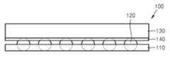
100,200,300...면광원 장치 110...제1기판
120...글래스 비드 130...제2기판
140...접착물질층1A to 1C are views illustrating a method for manufacturing a surface light source device according to an embodiment of the present invention.
2A to 2B are views for explaining a method for manufacturing a surface light source device according to another embodiment of the present invention.
3 shows an optical path through which light is emitted from the manufactured surface light source device.
4 is a graph showing the luminance represented by the surface light source device according to the depth of the glass beads immersed in the adhesive layer.
5 is a view for explaining a method for manufacturing a surface light source device according to another embodiment.
6 is a view for explaining a method for manufacturing a surface light source device according to another embodiment.
<Explanation of symbols for the main parts of the drawings>
100,200,300 ... plane
120
140 ... Adhesive Layer
이하, 첨부된 도면을 참조하여 본 발명의 바람직한 실시예를 상세히 설명하기로 한다. 이하의 도면들에서 동일한 참조부호는 동일한 구성요소를 지칭하며, 도면상에서 각 구성요소의 크기는 설명의 명료성과 편의상 과장되어 있을 수 있다.Hereinafter, exemplary embodiments of the present invention will be described in detail with reference to the accompanying drawings. In the drawings, like reference numerals refer to like elements, and the size of each element in the drawings may be exaggerated for clarity and convenience of description.
도 1a 내지 도 1c는 본 발명의 실시예에 의한 면광원 장치 제조방법을 설명하는 도면들이다.1A to 1C are views illustrating a method for manufacturing a surface light source device according to an embodiment of the present invention.
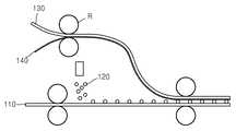
먼저, 도 1a를 참조하면, 제1기판(110)과 복수의 글래스 비드(120)를 포함하는 구조물을 형성한다. 복수의 글래스 비드(120) 각각은 일부 영역이 제1기판(110)의 내부에 임베드(embed)되고 나머지 영역은 제1기판(110)의 상부로 돌출된 형태이다. 이러한 형태는 용융 상태의 투명 물질에 글래스 비드(120)를 분산시킴으로써 형성할 수 있다.First, referring to FIG. 1A, a structure including a
글래스 비드(120)는 제조될 면광원장치에서 출사 구조를 형성하기 위해 제시되는 것이다. 도면에서, 글래스 비드(120)는 제1기판(110) 상에 일정한 조밀도로 분포하고 있으나, 이는 예시적인 것이며, 광원이 배치될 위치와 휘도 분포를 고려하여, 조밀도를 조절할 수 있다. 예를 들어, 광원으로부터 멀어질수록 조밀도가 커지도록 복수의 글래스 비드(120)의 분포를 정할 수 있다. 또한, 글래스 비드(120)의 크기도 일정하게 도시되어 있으나, 예시적인 것이며, 필요에 따라 가변될 수 있다. 투명 물질로는 PMMA(polymethyl methacrylate), PC(poly carbonate), 실리콘 러버와 같은 재질이 사용될 수 있다. 글래스 비드(120)의 굴절률을 대략 1.5 정도이며, 이와 실질적으로 동일한 굴절률을 갖도록 투명 물질을 선택한다. 글래스 비드(120) 일부 영역이 제1기판(110) 상부로 돌출되도록 제1기판(110)의 두께는 글래스 비드(120)의 직경보다 작은 크기를 가지도록 한다. 바람직하게는 반경 이하로 하며, 대략, 글래스 비드(120)의 반경 정도로 제1기판(110)의 두께를 정할 수 있다.
다음, 도 1b와 같이, 제2기판(130) 상에 접착물질층(140)을 형성한다. 접착물질층(140)으로는 예를 들어, PSA(pressure sensitive adhesive)를 사용할 수 있다. PSA는 압력을 가하면 가한 형상에 따라 접착력이 생기는 기능성 접착제이다. 제2기판(130)은 투명 재질로서 PMMA(polymethyl methacrylate), PC(poly carbonate), 실리콘 러버와 같은 재질이 사용될 수 있다. 또한, 글래스 비드(120)의 굴절률과 거의 같은 값의 굴절률을 갖도록, 제2기판(130)이나 접착물질층(140)의 재질을 선택한다.Next, as shown in FIG. 1B, the
다음, 도 1c와 같이 글래스 비드(120)의 돌출된 영역의 일부가 접착물질층(140) 내에 임베드되도록, 도 1a의 구조물과 도 1b의 구조물을 마주하게 배치되고, 접착물질층(140)이 경화됨으로써 도시된 면광원 장치(100)의 구조가 형성된다.Next, as shown in FIG. 1C, the structure of FIG. 1A and the structure of FIG. 1B are disposed to face each other so that a part of the protruding region of the
도 2a 내지 도 2b는 본 발명의 다른 실시예에 의한 면광원 장치 제조방법을 설명하는 도면들이다. 도 2a는 도 1a 내지 도 1c에서 설명한 과정이 롤 투 롤(roll to roll) 공정에 따라 행해지는 것을 보인다. 도면을 참조하면, 제1기판(110) 상에 글래스 비드(120)를 분사하며, 롤러를 통해 가열, 가압한다. 제2기판(130)과 접착물질층(140)도 롤러를 통해 접합된다. 다음, 제1기판(110) 상에 복수의 글래스 비드(120)가 형성된 구조물과 제2기판(130) 상에 접착물질층(140)이 형성된 구조물이 롤러를 통해 접합된다. 이와 같은 과정을 통해 도 2b와 같은 구조의 면광원 장치(100)가 형성된다. 이와 같이 롤 투 롤 공정을 사용하는 경우, 대형 구조로 형성하기가 용이하며, 대량 생산도 용이해진다.2A to 2B are views for explaining a method for manufacturing a surface light source device according to another embodiment of the present invention. 2A shows that the process described in FIGS. 1A-1C is performed according to a roll to roll process. Referring to the drawings, the
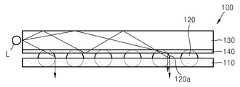
도 3은 제조된 면광원 장치(100)에서 광이 출사되는 광경로를 보인다. 광원(L)에서 조사된 광은 제2기판(130)의 내벽에서 전반사되며 내부를 진행하다가 글래스 비드(120)로 입사된다. 글래스 비드(120)의 측면(120a)에서 반사된 다음에는 전반사가 일어나지 않는 입사각으로 제1기판(110)의 면에 입사하여 외부로 출사된다.3 shows an optical path through which light is emitted from the manufactured surface
이와 같은 과정에 있어서, 글래스 비드(120)가 접착물질층(140)에 임베드된 깊이는 휘도 등의 광학 성능에 영향을 미치는 요소이다. 글래스 비드(120)가 접착물질층(140)에 임베드된 깊이는 실질적으로는 접착물질층(140)의 두께에 의해 정해지는데, 출사광의 휘도를 고려하여 접착물질층(140)의 두께를 정하는 것이 좋다. 접착물질층(140)의 두께는 대략, 글래스 비드(120) 반경의 10% 이내의 값을 갖도록 정할 수 있다.In this process, the depth of the
도 4는 글래스 비드(120)가 접착물질층(140)에 잠긴 깊이에 따라 면광원 장치(100)로부터 출사되는 광의 휘도를 보인 그래프이다. 그래프는 직경 50um의 글래스 비드(120)가 50um 간격으로 배치된 구조에서 접착물질층(140)의 두께에 따라 휘도를 전산 모사한 것이다. 그래프를 참조하면, 대략, 0.5um~1.5um 범위에서 휘도가 최대가 됨을 볼 수 있다.4 is a graph showing luminance of light emitted from the surface
도 5는 다른 실시예에 의한 면광원 장치 제조방법을 설명하는 도면이다. 도시된 면광원 장치(200)는 확산층(150)이 더 형성된 구조인 점에서, 도 1a 내지 도 1c에서 설명한 면광원 장치(100)와 차이가 있다. 확산층(150)은 제1기판(110)에서 글래스 비드(120)가 돌출된 면의 이면에 형성될 수 있다. 이러한 확산층(150)은 광이 보다 균일하게 혼합되어 출사되도록 하기 위해 마련될 수 있는데, 투명물질내에 예를 들어, topaz와 같은 산란 입자(scattering particle)(p)들을 임베드시켜서 형성할 수 있다.5 is a view for explaining a method for manufacturing a surface light source device according to another embodiment. The illustrated surface
확산층(150) 형성 과정은 도 1c의 과정, 즉, 제1기판(110)에 글래스 비드(120)가 형성된 구조물과 제2기판(130)상에 접착물질층(140)이 형성된 구조물이 접착되는 공정 다음에 수행될 수 있으며, 또는 그 전에 수행되는 것도 가능하다.The process of forming the
도면에서는 확산층(150)을 예시하여 설명하였으나, 필요에 따라, 확산층(150) 대신, 프리즘이나 렌즈 어레이가 더 형성될 수도 있다.In the drawing, the
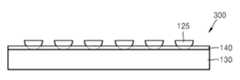
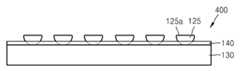
도 6은 다른 실시예에 의한 면광원 장치 제조방법을 설명하는 도면이다. 도면을 참조하면, 도 1c의 면광원 장치(100) 구조에서, 제1기판(110)과 제1기판(110)에 임베드된 글래스 비드(120)의 일부 영역이 제거된 구조이다. 즉, 제1기판(110)에 글래스 비드(120)가 형성된 구조물과 제2기판(130)상에 접착물질층(140)이 형성된 구조물이 접착되는 공정 다음에 제1기판(110)이 제거될 수 있다. 이러한 형상은 글래스 비드(120)를 절삭하거나, 또는, 제1기판(100)과 이에 임베드된 글래스 비드(120) 영역을 식각 또는 연마함으로써 형성할 수 있다. 반구형으로 절단된 글래스 비드(125)의 절단면이 광출사면이 된다. 본 실시예의 구조는 제1기판(100)이 제조 과정상의 필요에 의해 제시되는 것이며, 광학 성능에 있어서는 실질적인 영향을 미치지 않음을 고려한 것이다. 제1기판(110)이 제거됨으로써 보다 박형화된 구조가 된다.6 is a view for explaining a method for manufacturing a surface light source device according to another embodiment. Referring to the drawings, in the structure of the surface
도 7은 다른 실시예에 의한 면광원 장치 제조방법을 설명하는 도면이다. 면광원 장치(400)는 광출사면이 되는, 글래스 비드(125)의 절단면에 스크래치 구조(125a)를 형성한 것으로, 출사되는 광을 확산 혼합하는 역할을 할 수 있다.7 is a view for explaining a method for manufacturing a surface light source device according to another embodiment. The surface
이러한 본원 발명인 면광원 장치 제조방법은 이해를 돕기 위하여 도면에 도시된 실시예를 참고로 설명되었으나, 이는 예시적인 것에 불과하며, 당해 분야에서 통상적 지식을 가진 자라면 이로부터 다양한 변형 및 균등한 타 실시예가 가능하다는 점을 이해할 것이다. 따라서, 본 발명의 진정한 기술적 보호 범위는 첨부된 특허청구범위에 의해 정해져야 할 것이다. Such a method of manufacturing the surface light source device of the present invention has been described with reference to the embodiment shown in the drawings for clarity, but this is only an example, and those skilled in the art may various modifications and other equivalents therefrom. It will be appreciated that examples are possible. Therefore, the true technical protection scope of the present invention will be defined by the appended claims.
Claims (16)
Translated fromKorean제2기판 상에 접착물질층이 형성된 제2구조물을 형성하는 단계;
상기 글래스 비드의 돌출된 영역의 일부가 상기 접착물질층 내에 임베드되도록, 제1구조물과 상기 제2구조물을 접착하는 단계;를 포함하는 면광원 장치 제조방법.Forming a first structure having a first substrate and a plurality of glass beads, wherein a portion of each of the glass beads is embedded in the first substrate, and the remaining regions protrude to the upper portion of the first substrate. ;
Forming a second structure having an adhesive material layer formed on the second substrate;
Bonding the first structure and the second structure such that a portion of the protruding region of the glass bead is embedded in the adhesive material layer.
상기 제1구조물을 형성하는 단계는,
용융 상태의 투명 물질에 글래스 비드를 분산시킴으로써 상기 제1구조물을 형성하는 면광원 장치 제조방법.The method of claim 1,
Forming the first structure,
And dispersing glass beads in a transparent material in a molten state to form the first structure.
상기 투명 물질은 PMMA, PC, 실리콘 러버 중 어느 하나로 이루어지는 면광원 장치 제조방법.The method of claim 2,
The transparent material is a surface light source device manufacturing method made of any one of PMMA, PC, silicon rubber.
상기 제1기판의 두께는 상기 글래스 비드의 반경 이하인 면광원 장치 제조방법.The method of claim 1,
And a thickness of the first substrate is less than or equal to the radius of the glass beads.
상기 접착물질층의 두께는 대략, 상기 글래스 비드의 반경의 10% 이내인 면광원 장치 제조방법.The method of claim 1,
And the thickness of the adhesive material layer is approximately 10% of the radius of the glass beads.
롤 투 롤(roll to roll) 공정에 의해 상기 제1구조물과 제2구조물의 형성과 상호 접착이 수행되는 면광원 장치 제조방법.The method of claim 1,
A method of manufacturing a surface light source device in which formation and mutual bonding of the first structure and the second structure are performed by a roll to roll process.
상기 제1기판에서 상기 복수의 글래스 비드가 돌출된 면의 이면에 확산층을 형성하는 단계를 더 포함하는 면광원 장치 제조방법.The method of claim 1,
The method of claim 1, further comprising forming a diffusion layer on a rear surface of the first substrate to which the plurality of glass beads protrude.
상기 확산층은 투명기판내에 복수의 산란 입자들이 임베드된 형태로 이루어지는 면광원 장치 제조방법.The method of claim 7, wherein
The diffusion layer is a surface light source device manufacturing method comprising a plurality of scattering particles embedded in a transparent substrate.
상기 확산 입자는 Topaz인 면광원 장치 제조방법.The method of claim 8,
The diffusion particle is a surface light source device manufacturing method of Topaz.
상기 확산층 형성 단계는 상기 제1구조물과 제2구조물이 접착된 다음에 수행되는 면광원 장치 제조방법.The method of claim 7, wherein
The diffusing layer forming step is performed after the first structure and the second structure is bonded.
상기 확산층 형성 단계는 상기 제1구조물과 제2구조물이 접착되기 전에 수행되는 면광원 장치 제조방법.The method of claim 7, wherein
The diffusion layer forming step is performed before the first structure and the second structure is bonded.
상기 제1구조물과 제2구조물이 접착된 후, 상기 제1기판과 상기 제1기판에 임베드된 글래스 비드의 일부 영역을 제거하는 단계를 더 포함하는 면광원 장치 제조방법.The method of claim 1,
And after removing the first structure and the second structure, removing a portion of the glass beads embedded in the first substrate and the first substrate.
상기 제1기판 및 상기 제1기판에 임베드된 글래스 비드의 일부 영역이 식각 공정 또는 연마 공정에 의해 제거되는 면광원 장치 제조방법.The method of claim 12,
And a portion of the glass bead embedded in the first substrate and the first substrate is removed by an etching process or a polishing process.
상기 제1기판의 제거에 따라 노출되는 상기 글래스 비드의 절단면에 출사광 확산을 위한 스크래치 구조를 형성하는 단계를 더 포함하는 면광원 장치 제조방법.The method of claim 12,
And forming a scratch structure for diffusing outgoing light on the cut surface of the glass bead exposed by the removal of the first substrate.
상기 제2기판은 PMMA, PC, 실리콘 러버 중 어느 하나로 이루어지는 면광원 장치 제조방법.The method according to any one of claims 1 to 14,
The second substrate is a surface light source device manufacturing method consisting of any one of PMMA, PC, silicon rubber.
상기 접착물질층은 PSA(pressure sensitive adhesive)로 이루어지는 면광원 장치 제조방법.The method according to any one of claims 1 to 14,
The adhesive material layer is a surface light source device manufacturing method consisting of a pressure sensitive adhesive (PSA).
Priority Applications (2)
| Application Number | Priority Date | Filing Date | Title |
|---|---|---|---|
| KR1020100000903AKR101687016B1 (en) | 2010-01-06 | 2010-01-06 | Method of manufacturing a surface light source device |
| US12/926,126US8685261B2 (en) | 2010-01-06 | 2010-10-27 | Methods of manufacturing surface light source devices |
Applications Claiming Priority (1)
| Application Number | Priority Date | Filing Date | Title |
|---|---|---|---|
| KR1020100000903AKR101687016B1 (en) | 2010-01-06 | 2010-01-06 | Method of manufacturing a surface light source device |
Publications (2)
| Publication Number | Publication Date |
|---|---|
| KR20110080592Atrue KR20110080592A (en) | 2011-07-13 |
| KR101687016B1 KR101687016B1 (en) | 2016-12-16 |
Family
ID=44224110
Family Applications (1)
| Application Number | Title | Priority Date | Filing Date |
|---|---|---|---|
| KR1020100000903AExpired - Fee RelatedKR101687016B1 (en) | 2010-01-06 | 2010-01-06 | Method of manufacturing a surface light source device |
Country Status (2)
| Country | Link |
|---|---|
| US (1) | US8685261B2 (en) |
| KR (1) | KR101687016B1 (en) |
Families Citing this family (10)
| Publication number | Priority date | Publication date | Assignee | Title |
|---|---|---|---|---|
| KR101934427B1 (en)* | 2012-05-31 | 2019-01-03 | 엘지이노텍 주식회사 | Illuminating device |
| TW201426037A (en)* | 2012-12-26 | 2014-07-01 | Hon Hai Prec Ind Co Ltd | Light guide plate and making method thereof |
| TWI548918B (en)* | 2015-04-13 | 2016-09-11 | 揚昇照明股份有限公司 | Light source module |
| KR102155405B1 (en)* | 2016-04-15 | 2020-09-14 | 주식회사 엘지화학 | Light guide plate unit, back light unit and liquid crystal display comprising the same |
| DE102016118885A1 (en) | 2016-10-05 | 2018-04-05 | Temicon Gmbh | Light-deflecting device, method of manufacturing a light-deflecting device and lighting device |
| CN106597599A (en)* | 2017-01-17 | 2017-04-26 | 京东方科技集团股份有限公司 | Backlight module, display panel and display device |
| KR102526416B1 (en)* | 2018-06-25 | 2023-04-27 | 삼성디스플레이 주식회사 | Optical member, display including the same and method for fabricating the optical member |
| CN108873150A (en)* | 2018-07-11 | 2018-11-23 | 东莞市银泰丰光学科技有限公司 | A kind of microstructured glass leaded light board machining process |
| CN111694077B (en)* | 2020-06-24 | 2021-08-17 | 电子科技大学 | A kind of hemispherical microlens and preparation method thereof |
| CN111999786A (en)* | 2020-09-11 | 2020-11-27 | 电子科技大学 | Hemispherical lens with opaque film covering spherical center and preparation method thereof |
Citations (4)
| Publication number | Priority date | Publication date | Assignee | Title |
|---|---|---|---|---|
| US6060157A (en)* | 1994-11-29 | 2000-05-09 | 3M Innovative Properties Company | Transparent decorative article having an etched appearing/prismatic image thereon |
| KR20010053475A (en)* | 1998-07-10 | 2001-06-25 | 가나이 쓰토무 | Luminous intensity distribution control device and display having the same |
| JP2005215166A (en)* | 2004-01-28 | 2005-08-11 | Dainippon Printing Co Ltd | Transfer substrate for forming single particle film, method for forming single particle film using transfer substrate, and electrophoretic display device |
| KR20080109659A (en)* | 2007-06-12 | 2008-12-17 | 이터널 케미컬주식회사 | Optical film |
Family Cites Families (6)
| Publication number | Priority date | Publication date | Assignee | Title |
|---|---|---|---|---|
| US7160017B2 (en) | 2004-06-03 | 2007-01-09 | Eastman Kodak Company | Brightness enhancement film using a linear arrangement of light concentrators |
| CN1766704A (en) | 2004-10-29 | 2006-05-03 | 清华大学 | Light guide plate and surface emitting device |
| WO2006093087A1 (en) | 2005-02-28 | 2006-09-08 | Kuraray Co., Ltd. | Photodiffusion film, planar light source element using the same, and liquid crystal display device |
| KR101345375B1 (en) | 2006-03-28 | 2013-12-31 | 삼성전자주식회사 | all-in-one type light guide plate, backlighting apparatus employing the same and Method for manufacturing the same |
| JP2007329007A (en) | 2006-06-07 | 2007-12-20 | Omron Corp | Point light source backlight, and liquid crystal display device |
| US10105875B2 (en)* | 2008-08-21 | 2018-10-23 | Cam Holding Corporation | Enhanced surfaces, coatings, and related methods |
- 2010
- 2010-01-06KRKR1020100000903Apatent/KR101687016B1/ennot_activeExpired - Fee Related
- 2010-10-27USUS12/926,126patent/US8685261B2/ennot_activeExpired - Fee Related
Patent Citations (4)
| Publication number | Priority date | Publication date | Assignee | Title |
|---|---|---|---|---|
| US6060157A (en)* | 1994-11-29 | 2000-05-09 | 3M Innovative Properties Company | Transparent decorative article having an etched appearing/prismatic image thereon |
| KR20010053475A (en)* | 1998-07-10 | 2001-06-25 | 가나이 쓰토무 | Luminous intensity distribution control device and display having the same |
| JP2005215166A (en)* | 2004-01-28 | 2005-08-11 | Dainippon Printing Co Ltd | Transfer substrate for forming single particle film, method for forming single particle film using transfer substrate, and electrophoretic display device |
| KR20080109659A (en)* | 2007-06-12 | 2008-12-17 | 이터널 케미컬주식회사 | Optical film |
Also Published As
| Publication number | Publication date |
|---|---|
| KR101687016B1 (en) | 2016-12-16 |
| US8685261B2 (en) | 2014-04-01 |
| US20110163066A1 (en) | 2011-07-07 |
Similar Documents
| Publication | Publication Date | Title |
|---|---|---|
| KR20110080592A (en) | Method of manufacturing surface light source device | |
| TWI655464B (en) | Light guide plate, surface light source device, display device and electronic device | |
| US8128800B2 (en) | Method of manufacturing light guide panel with pattern accuracy | |
| KR20090055137A (en) | Method of manufacturing a reflective display device and a light guide plate | |
| US8351119B2 (en) | Multi-coated hybrid optical film structure | |
| JP2008040480A (en) | Optical plate, method for manufacturing the same, and backlight using the optical plate | |
| JP2010123569A (en) | Backlight assembly using flexible light guide film and liquid crystal display module including the same | |
| CN108730921B (en) | Light guide module, total reflection type display device and method for manufacturing light guide module | |
| CN210244014U (en) | Backlight module, display screen and mobile terminal | |
| CN101329414A (en) | Light-collecting composite sheet | |
| KR20120036293A (en) | Back light guide plate and manufacturing method for the same | |
| CN100409037C (en) | Light control film and backlight device using the same | |
| CN113311530B (en) | Light source assembly and display device | |
| TWI354838B (en) | Backlight module and method for manufacturing the | |
| JP2005134441A (en) | Light guide and method for manufacturing the same, and liquid crystal display device | |
| TW201209461A (en) | Light guide plate with light entrance structure and manufacture method for manufacturing the same | |
| CN101408629A (en) | Backlight module unit and prism lens | |
| KR20140011702A (en) | Backlight assembly | |
| KR20160047440A (en) | Light guide plate including optical sheet and backlight unit containing the same | |
| JP2009294240A (en) | Optical sheet, back light unit, liquid crystal display device and display device | |
| TW201510620A (en) | Thin shape direct back light module | |
| CN116381986A (en) | Glass lamp panel assembly and method of manufacturing the same | |
| CN101329415A (en) | Light-collecting composite sheet | |
| CN204650015U (en) | Thin light guide plate | |
| KR101210986B1 (en) | Condensing film for backlight unit |
Legal Events
| Date | Code | Title | Description |
|---|---|---|---|
| PA0109 | Patent application | St.27 status event code:A-0-1-A10-A12-nap-PA0109 | |
| PG1501 | Laying open of application | St.27 status event code:A-1-1-Q10-Q12-nap-PG1501 | |
| R18-X000 | Changes to party contact information recorded | St.27 status event code:A-3-3-R10-R18-oth-X000 | |
| A201 | Request for examination | ||
| PA0201 | Request for examination | St.27 status event code:A-1-2-D10-D11-exm-PA0201 | |
| D13-X000 | Search requested | St.27 status event code:A-1-2-D10-D13-srh-X000 | |
| D14-X000 | Search report completed | St.27 status event code:A-1-2-D10-D14-srh-X000 | |
| E902 | Notification of reason for refusal | ||
| PE0902 | Notice of grounds for rejection | St.27 status event code:A-1-2-D10-D21-exm-PE0902 | |
| P22-X000 | Classification modified | St.27 status event code:A-2-2-P10-P22-nap-X000 | |
| P11-X000 | Amendment of application requested | St.27 status event code:A-2-2-P10-P11-nap-X000 | |
| P13-X000 | Application amended | St.27 status event code:A-2-2-P10-P13-nap-X000 | |
| E701 | Decision to grant or registration of patent right | ||
| PE0701 | Decision of registration | St.27 status event code:A-1-2-D10-D22-exm-PE0701 | |
| GRNT | Written decision to grant | ||
| PR0701 | Registration of establishment | St.27 status event code:A-2-4-F10-F11-exm-PR0701 | |
| PR1002 | Payment of registration fee | St.27 status event code:A-2-2-U10-U11-oth-PR1002 Fee payment year number:1 | |
| PG1601 | Publication of registration | St.27 status event code:A-4-4-Q10-Q13-nap-PG1601 | |
| FPAY | Annual fee payment | Payment date:20191115 Year of fee payment:4 | |
| PR1001 | Payment of annual fee | St.27 status event code:A-4-4-U10-U11-oth-PR1001 Fee payment year number:4 | |
| PC1903 | Unpaid annual fee | St.27 status event code:A-4-4-U10-U13-oth-PC1903 Not in force date:20201210 Payment event data comment text:Termination Category : DEFAULT_OF_REGISTRATION_FEE | |
| PC1903 | Unpaid annual fee | St.27 status event code:N-4-6-H10-H13-oth-PC1903 Ip right cessation event data comment text:Termination Category : DEFAULT_OF_REGISTRATION_FEE Not in force date:20201210 |