KR20110080318A - Light emitting device package - Google Patents
Light emitting device packageDownload PDFInfo
- Publication number
- KR20110080318A KR20110080318AKR1020100000486AKR20100000486AKR20110080318AKR 20110080318 AKR20110080318 AKR 20110080318AKR 1020100000486 AKR1020100000486 AKR 1020100000486AKR 20100000486 AKR20100000486 AKR 20100000486AKR 20110080318 AKR20110080318 AKR 20110080318A
- Authority
- KR
- South Korea
- Prior art keywords
- light emitting
- emitting device
- layer
- electrode layer
- device package
- Prior art date
- Legal status (The legal status is an assumption and is not a legal conclusion. Google has not performed a legal analysis and makes no representation as to the accuracy of the status listed.)
- Ceased
Links
Images
Classifications
- H—ELECTRICITY
- H10—SEMICONDUCTOR DEVICES; ELECTRIC SOLID-STATE DEVICES NOT OTHERWISE PROVIDED FOR
- H10H—INORGANIC LIGHT-EMITTING SEMICONDUCTOR DEVICES HAVING POTENTIAL BARRIERS
- H10H20/00—Individual inorganic light-emitting semiconductor devices having potential barriers, e.g. light-emitting diodes [LED]
- H10H20/80—Constructional details
- H10H20/85—Packages
- H10H20/851—Wavelength conversion means
- H10H20/8514—Wavelength conversion means characterised by their shape, e.g. plate or foil
- H—ELECTRICITY
- H10—SEMICONDUCTOR DEVICES; ELECTRIC SOLID-STATE DEVICES NOT OTHERWISE PROVIDED FOR
- H10H—INORGANIC LIGHT-EMITTING SEMICONDUCTOR DEVICES HAVING POTENTIAL BARRIERS
- H10H20/00—Individual inorganic light-emitting semiconductor devices having potential barriers, e.g. light-emitting diodes [LED]
- H10H20/80—Constructional details
- H10H20/85—Packages
- H10H20/851—Wavelength conversion means
- H10H20/8515—Wavelength conversion means not being in contact with the bodies
- H—ELECTRICITY
- H10—SEMICONDUCTOR DEVICES; ELECTRIC SOLID-STATE DEVICES NOT OTHERWISE PROVIDED FOR
- H10H—INORGANIC LIGHT-EMITTING SEMICONDUCTOR DEVICES HAVING POTENTIAL BARRIERS
- H10H20/00—Individual inorganic light-emitting semiconductor devices having potential barriers, e.g. light-emitting diodes [LED]
- H10H20/80—Constructional details
- H10H20/85—Packages
- H10H20/852—Encapsulations
- H10H20/854—Encapsulations characterised by their material, e.g. epoxy or silicone resins
- H—ELECTRICITY
- H01—ELECTRIC ELEMENTS
- H01L—SEMICONDUCTOR DEVICES NOT COVERED BY CLASS H10
- H01L2224/00—Indexing scheme for arrangements for connecting or disconnecting semiconductor or solid-state bodies and methods related thereto as covered by H01L24/00
- H01L2224/01—Means for bonding being attached to, or being formed on, the surface to be connected, e.g. chip-to-package, die-attach, "first-level" interconnects; Manufacturing methods related thereto
- H01L2224/42—Wire connectors; Manufacturing methods related thereto
- H01L2224/47—Structure, shape, material or disposition of the wire connectors after the connecting process
- H01L2224/48—Structure, shape, material or disposition of the wire connectors after the connecting process of an individual wire connector
- H01L2224/4805—Shape
- H01L2224/4809—Loop shape
- H01L2224/48091—Arched
- H—ELECTRICITY
- H01—ELECTRIC ELEMENTS
- H01L—SEMICONDUCTOR DEVICES NOT COVERED BY CLASS H10
- H01L2224/00—Indexing scheme for arrangements for connecting or disconnecting semiconductor or solid-state bodies and methods related thereto as covered by H01L24/00
- H01L2224/80—Methods for connecting semiconductor or other solid state bodies using means for bonding being attached to, or being formed on, the surface to be connected
- H01L2224/85—Methods for connecting semiconductor or other solid state bodies using means for bonding being attached to, or being formed on, the surface to be connected using a wire connector
- H01L2224/85909—Post-treatment of the connector or wire bonding area
- H01L2224/8592—Applying permanent coating, e.g. protective coating
- H—ELECTRICITY
- H01—ELECTRIC ELEMENTS
- H01L—SEMICONDUCTOR DEVICES NOT COVERED BY CLASS H10
- H01L2924/00—Indexing scheme for arrangements or methods for connecting or disconnecting semiconductor or solid-state bodies as covered by H01L24/00
- H01L2924/15—Details of package parts other than the semiconductor or other solid state devices to be connected
- H01L2924/181—Encapsulation
- H—ELECTRICITY
- H10—SEMICONDUCTOR DEVICES; ELECTRIC SOLID-STATE DEVICES NOT OTHERWISE PROVIDED FOR
- H10H—INORGANIC LIGHT-EMITTING SEMICONDUCTOR DEVICES HAVING POTENTIAL BARRIERS
- H10H20/00—Individual inorganic light-emitting semiconductor devices having potential barriers, e.g. light-emitting diodes [LED]
- H10H20/80—Constructional details
- H10H20/85—Packages
- H10H20/8506—Containers
- H—ELECTRICITY
- H10—SEMICONDUCTOR DEVICES; ELECTRIC SOLID-STATE DEVICES NOT OTHERWISE PROVIDED FOR
- H10H—INORGANIC LIGHT-EMITTING SEMICONDUCTOR DEVICES HAVING POTENTIAL BARRIERS
- H10H20/00—Individual inorganic light-emitting semiconductor devices having potential barriers, e.g. light-emitting diodes [LED]
- H10H20/80—Constructional details
- H10H20/85—Packages
- H10H20/852—Encapsulations
- H10H20/853—Encapsulations characterised by their shape
Landscapes
- Led Device Packages (AREA)
- Electroluminescent Light Sources (AREA)
Abstract
Translated fromKoreanDescription
Translated fromKorean실시예는 발광 소자 패키지에 관한 것이다.Embodiments relate to a light emitting device package.
발광 다이오드(Light Emitting Diode: LED)는 전류를 빛으로 변환시키는 발광 소자이다.Light emitting diodes (LEDs) are light emitting devices that convert current into light.
이러한 LED에 의해 방출되는 빛의 파장은 LED를 제조하는데 사용되는 반도체 재료에 따른다. 이는 방출된 빛의 파장이 가전자대(valence band) 전자들과 전도대(conduction band) 전자들 사이의 에너지 차를 나타내는 반도체 재료의 밴드갭(band-gap)에 따르기 때문이다.The wavelength of light emitted by these LEDs depends on the semiconductor material used to make the LEDs. This is because the wavelength of the emitted light depends on the band-gap of the semiconductor material, which represents the energy difference between the valence band electrons and the conduction band electrons.
최근 발광 다이오드(Light Emitting Diode; LED)는 휘도가 점차 증가하게 되어 디스플레이용 광원, 자동차용 광원 및 조명용 광원으로 사용되고 있으며, 형광 물질을 이용하거나 다양한 색의 LED를 조합함으로써 효율이 우수한 백색 광을 발광하는 LED도 구현이 가능하다.In recent years, light emitting diodes (LEDs) have been gradually increased in brightness and are used as light sources for displays, automotive light sources, and lighting sources, and emit highly efficient white light by using fluorescent materials or by combining LEDs of various colors. LED can be implemented.
실시예는 새로운 구조를 갖는 발광 소자 패키지를 제공한다.The embodiment provides a light emitting device package having a new structure.
실시예는 색 편차가 감소된 빛을 방출하는 발광 소자 패키지를 제공한다.The embodiment provides a light emitting device package that emits light with reduced color deviation.
실시예에 따른 발광 소자 패키지는 몸체부; 상기 몸체부 상에 제1 전극층 및 제2 전극층; 상기 몸체부 상에 배치되고, 상기 제1 전극층 및 제2 전극층과 전기적으로 연결되는 발광 소자; 상기 발광 소자를 포위하는 형광체층; 및 상기 형광체층 상에 파티클을 포함하는 봉지층을 포함한다.The light emitting device package according to the embodiment includes a body portion; A first electrode layer and a second electrode layer on the body portion; A light emitting element disposed on the body portion and electrically connected to the first electrode layer and the second electrode layer; A phosphor layer surrounding the light emitting element; And an encapsulation layer including particles on the phosphor layer.
실시예는 새로운 구조를 갖는 발광 소자 패키지를 제공할 수 있다.The embodiment can provide a light emitting device package having a new structure.
실시예는 색 편차가 감소된 빛을 방출하는 발광 소자 패키지를 제공할 수 있다.The embodiment can provide a light emitting device package that emits light with reduced color deviation.
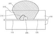
도 1은 제1 실시예에 따른 발광 소자 패키지를 설명하는 도면.
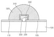
도 2는 제2 실시예에 따른 발광 소자 패키지를 설명하는 도면.
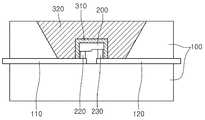
도 3은 제3 실시예에 따른 발광 소자 패키지를 설명하는 도면.1 is a view for explaining a light emitting device package according to the first embodiment.
2 is a view for explaining a light emitting device package according to the second embodiment;
3 is a view for explaining a light emitting device package according to the third embodiment;
실시예의 설명에 있어서, 각 층(막), 영역, 패턴 또는 구조물들이 기판, 각 층(막), 영역, 패드 또는 패턴들의 "상/위(on)"에 또는 "하/아래(under)"에 형성되는 것으로 기재되는 경우에 있어, "상/위(on)"와 "하/아래(under)"는 "직접(directly)" 또는 "다른 층을 개재하여 (indirectly)" 형성되는 것을 모두 포함한다. 또한 각 층의 상/위 또는 하/아래에 대한 기준은 도면을 기준으로 설명한다.In the description of an embodiment, each layer, region, pattern or structure may be "under" or "under" the substrate, each layer, region, pad or pattern. In the case where it is described as being formed at, "up" and "under" include both "directly" or "indirectly" formed through another layer. do. In addition, the criteria for up / down or down / down each layer will be described with reference to the drawings.
도면에서 각층의 두께나 크기는 설명의 편의 및 명확성을 위하여 과장되거나 생략되거나 또는 개략적으로 도시되었다. 또한 각 구성요소의 크기는 실제크기를 전적으로 반영하는 것은 아니다.In the drawings, the thickness or size of each layer is exaggerated, omitted, or schematically illustrated for convenience and clarity of description. In addition, the size of each component does not necessarily reflect the actual size.
이하, 첨부된 도면을 참조하여 실시예들에 따른 발광 소자 패키지에 대해 상세히 설명하도록 한다.Hereinafter, a light emitting device package according to embodiments will be described in detail with reference to the accompanying drawings.
도 1은 제1 실시예에 따른 발광 소자 패키지를 설명하는 도면이다.1 is a view illustrating a light emitting device package according to a first embodiment.
도 1을 참조하면, 제1 실시예에 따른 발광 소자 패키지는 몸체부(100)와, 상기 몸체부(100)에 설치된 제1 전극층(110) 및 제2 전극층(120)과, 상기 몸체부(100)에 설치되어 상기 제1 전극층(110) 및 제2 전극층(120)과 전기적으로 연결되는 발광 소자(200)와, 상기 발광 소자(200)를 포위하는 형광체층(310)과, 상기 형광체층(310) 상에 형성된 봉지층(320)을 포함한다.Referring to FIG. 1, the light emitting device package according to the first embodiment includes a
상기 몸체부(100)는 실리콘 재질, 합성수지 재질, 또는 금속 재질을 포함하여 형성될 수 있으며, 상기 몸체부(100)에는 상기 발광 소자(200)의 주위를 둘러싸는 경사면이 형성된 캐비티가 포함될 수 있고, 상기 경사면에는 반사층(미도시)이 형성될 수도 있다.The
상기 제1 전극층(110) 및 제2 전극층(120)은 서로 전기적으로 분리되고, 상기 몸체부(100)를 관통하여 형성될 수 도 있으며, 상기 발광 소자(200)에 전원을 제공하는 역할을 한다. 또한, 상기 제1 전극층(110) 및 제2 전극층(120)은 상기 발광 소자(200)에서 발생된 빛을 반사시켜 광 효율을 증가시키는 역할을 할 수 있으며, 상기 발광 소자(200)에서 발생된 열을 외부로 배출시키는 역할을 할 수도 있다.The
상기 발광 소자(200)는 n측 전극층과 p측 전극층이 모두 발광 소자 구조물의 상면에 배치되는 수평형 타입의 발광 소자, n측 전극층과 p측 전극층이 모두 발광 소자 구조물의 하면에 배치되는 플립칩 타입의 발광 소자, 또는 n측 전극층과 p측 전극층이 각각 발광 소자 구조물의 상면과 하면에 배치되는 수직형 타입의 발광 소자가 적용될 수 있다. 도 1에는 수직형 타입의 발광 소자가 예시되어 있으며, 상기 발광 소자(200)의 n측 전극층은 와이어(210)를 통해 제1 전극층(110)과 전기적으로 연결되고 상기 발광 소자(200)의 p측 전극층은 상기 제2 전극층(120)과 접촉하여 연결된다. 예를 들어, 상기 발광 소자(200)는 n형 반도체층, 활성층, p형 반도체층을 포함하는 발광 다이오드로 형성될 수 있다.The
상기 발광 소자(200)는 상기 몸체부(100) 상에 설치되거나 상기 제1 전극층(110) 또는 제2 전극층(120) 상에 설치될 수 있다. 도 1에는 상기 발광 소자(200)가 제2 전극층(120) 상에 설치된 것이 예시되어 있다.The
상기 형광체층(310)은 상기 몸체부(100) 상에 형성되어 상기 발광 소자(200)를 포위하고, 상기 봉지층(320)은 상기 형광체층(310) 상에 형성된다. 상기 형광체층(310)은 상기 발광 소자(200)에서 발생된 빛을 색 변환하는 역할을 하고, 상기 봉지층(320)은 상기 형광체층(310)을 보호하는 보호층 역할과 함께 상기 발광 소자(200)에서 방출된 빛의 지향각을 제어하는 렌즈의 역할을 한다. 상기 봉지층(320)은 상면이 볼록하게 형성되어 상기 봉지층(320)을 통해 외부로 방출되는 빛이 상기 봉지층(3200과 외부의 경계면에서 전반사되는 양을 감소시킨다.The
상기 형광체층(310)은 실리콘 젤 또는 에폭시에 형광체를 분산시켜 형성할 수 있으며, 상기 봉지층(320)은 실리콘 젤 또는 에폭시에 상기 실리콘 젤 또는 에폭시 보다 굴절률이 큰 고굴절 파티클을 분산시켜 형성할 수 있다.The
실시예에서 상기 형광체층(310)과 상기 봉지층(320)은 굴절률이 서로 매칭된다. 상기 형광체층(310)은 제1 굴절률을 갖고 상기 봉지층(320)은 상기 제1 굴절률과 동일하거나 10%이하의 편차를 갖는 제2 굴절률을 갖는다. 예를 들어, 상기 형광체층(310)의 굴절률이 1.7인 경우, 상기 봉지층(320)의 굴절률은 1.53~1.87의 굴절률을 갖는다.In an embodiment, the
상기 형광체층(310)의 굴절률과 봉지층(320)의 굴절률의 차이가 큰 경우, 상기 발광 소자(200)에서 방출된 광은 상기 형광체층(310)을 지나 상기 형광체층(310)과 봉지층(320) 사이의 경계면에서 전반사되어 다시 상기 형광체층(310)에서 진행하다가 외부로 방출될 가능성이 증가된다. 이때, 상기 발광 소자(200)에서 방출된 광 중 상기 경계면에서 전반사되지 않고 바로 방출된 광과, 상기 경계면에서 전반사되어 다시 상기 형광체층(310)을 진행하다가 방출된 광은 색 변환 정도에 있어서 차이를 갖게 되고 이것이 발광 소자(200)의 색 편차를 가져온다.When the difference between the refractive index of the
따라서, 실시예에 따른 발광 소자 패키지는 상기 형광체층(310)의 굴절률과 봉지층(320)의 굴절률을 동일하거나 유사하게 조절함으로써 상기 발광 소자(200)에서 방출된 광의 색 편차를 감소시킨다.Therefore, the light emitting device package according to the embodiment reduces the color deviation of the light emitted from the
예를 들어, 상기 형광체층(310)은 굴절률이 1.4~1.6인 실리콘 젤에 굴절률이 대략 1.8인 야그(YAG)계 형광체 또는 굴절률이 대략 2.0인 실리케이트계 형광체를 혼합하여 형성하며, 상기 형광체층(310)은 1.6~1.8의 유효 굴절률을 갖는다. 한편, 상기 봉지층(320)은 굴절률이 1.4~1.6인 실리콘 젤을 사용하여 형성할 수 있는데, 이 경우 상기 형광체층(310)과 봉지층(320)의 굴절률 차이에 의해 상기 경계면에서의 전반사가 증가하게 된다.For example, the
따라서, 실시예에서는 상기 봉지층(320)에 파티클을 혼합하여 상기 봉지층(320)의 유효 굴절률이 상기 형광체층(310)의 유효 굴절률과 유사하도록 조절한다.Therefore, in an embodiment, particles are mixed with the
상기 파티클은 고굴절 파티클이 사용될 수 있고, 예를 들어, 금속 산화물이 사용될 수 있으며, TiO2, Al2O3, TaO2, CeO2, 실리카 중 적어도 어느 하나가 사용될 수 있다. 상기 봉지층(320)에 상기 파티클이 포함되는 경우, 상기 봉지층(320)의 유효 굴절률은 1.6~1.8로 증가된다.The particle may be a high refractive particle, for example, a metal oxide may be used, and at least one of TiO2 , Al2 O3 , TaO2 , CeO2 , silica may be used. When the particles are included in the
따라서, 상기 형광체층(310)과 상기 봉지층(320)의 굴절률은 동일하거나 유사하게 되어 상기 형광체층(310)과 봉지층(320) 사이의 경계면에서 전반사가 감소되며, 결과적으로, 상기 발광 소자(200)에서 방출되는 빛의 색 편차가 감소될 수 있다.Therefore, the refractive indexes of the
도 2는 제2 실시예에 따른 발광 소자 패키지를 설명하는 도면이다.2 is a view illustrating a light emitting device package according to a second embodiment.
제2 실시예에 따른 발광 소자 패키지를 설명함에 있어서 제1 실시예에 따른 발광 소자 패키지에 대한 설명과 중복되는 설명을 생략하도록 한다.In the description of the light emitting device package according to the second embodiment, a description overlapping with the description of the light emitting device package according to the first embodiment will be omitted.
도 2를 참조하면, 제2 실시예에 따른 발광 소자 패키지는 몸체부(100)와, 상기 몸체부(100)에 설치된 제1 전극층(110) 및 제2 전극층(120)과, 상기 제1 전극층(110) 및 제2 전극층(120) 상에 배치되어 상기 제1 전극층(110) 및 제2 전극층(120)과 전기적으로 연결되는 발광 소자(200)와, 상기 발광 소자(200)를 포위하는 형광체층(310)과, 상기 형광체층(310)을 포위하는 봉지층(320)을 포함한다.Referring to FIG. 2, the light emitting device package according to the second embodiment may include a
상기 몸체부(100)는 상면이 평평한 기판 형태로 형성될 수 있으며, 상기 몸체부(100) 상에는 반사층(미도시)이 형성될 수 있다. 또한, 상기 제1 전극층(110) 및 제2 전극층(120)은 상기 반사층의 역할을 수행할 수도 있다.The
상기 발광 소자(200)는 제1 범프(220) 및 제2 범프(230)를 통해 상기 제1 전극층(110) 및 제2 전극층(120)과 전기적으로 연결되는 플립칩 타입의 발광 소자가 사용될 수 있다.The
상기 형광체층(310)은 상기 발광 소자(200)의 주위에 실질적으로 균일한 두께로 형성될 수 있다. 즉, 상기 형광체층(310)은 컨포멀 코팅(conformal coating)으로 도포될 수 있다. 다른 예로서, 상기 형광체층(310)은 형광체가 포함된 필름으로 형성될 수 있다.The
상기 봉지층(320)은 상기 형광체층(310), 제1 전극층(110), 및 제2 전극층(120) 상에 형성된다.The
상기 형광체층(310)을 컨포멀 코팅으로 형성하는 이유는 상기 발광 소자(200)에서 방출된 빛이 균일한 두께의 형광체층(310)을 지나도록 하여 색 편차를 감소시키기 위함이다. 그러나, 상기 형광체층(310)을 균일한 두께로 형성한다고 하더라도 상기 형광체층(310)과 봉지층(320) 사이의 굴절률 차이가 큰 경우, 발광 소자(200)에서 방출된 빛 중 일부는 상기 형광체층(310)과 봉지층(320) 사이의 경계에서 전반사되어 다시 상기 형광체층(310)을 진행하다가 외부로 방출된다. 따라서, 상기 형광체층(310)을 컨포멀 코팅하여도 상기 발광 소자(200)에서 방출된 빛의 색 편차를 감소시키는데 한계가 있다.The reason why the
앞서 제1 실시예에서 설명한 바와 같이, 상기 봉지층(320)은 고굴절 파티클을 분산시켜 형성함으로써 상기 형광체층(310)과 유효 굴절률이 유사하도록 조절할 수 있다.As described above in the first embodiment, the
따라서, 실시예에 따른 발광 소자 패키지는 상기 형광체층(310)과 봉지층(320)의 굴절률을 서로 동일하거나 유사하게 매칭시킴으로써, 상기 형광체층(310)과 봉지층(320) 사이의 경계에서 전반사되는 빛의 양을 감소시킨다.Accordingly, in the light emitting device package according to the embodiment, the total reflection at the boundary between the
도 3은 제3 실시예에 따른 발광 소자 패키지를 설명하는 도면이다.3 is a view illustrating a light emitting device package according to a third embodiment.
제3 실시예에 따른 발광 소자 패키지를 설명함에 있어서 제1 실시예 및 제2 실시예에 따른 발광 소자 패키지에 대한 설명과 중복되는 설명을 생략하도록 한다.In the description of the light emitting device package according to the third embodiment, a description overlapping with the description of the light emitting device package according to the first and second embodiments will be omitted.
도 3을 참조하면, 제3 실시예에 따른 발광 소자 패키지는 몸체부(100)와, 상기 몸체부(100)에 설치된 제1 전극층(110) 및 제2 전극층(120)과, 상기 제1 전극층(110) 및 제2 전극층(120) 상에 배치되어 상기 제1 전극층(110) 및 제2 전극층(120)과 전기적으로 연결되는 발광 소자(200)와, 상기 발광 소자(200)를 포위하는 형광체층(310)과, 상기 형광체층(310)을 포위하는 봉지층(320)을 포함한다.Referring to FIG. 3, the light emitting device package according to the third embodiment may include a
상기 몸체부(100)는 상기 발광 소자(200)의 주위를 둘러싸는 경사면을 포함할 수 있고, 상기 경사면에는 반사층(미도시)이 형성될 수도 있다.The
상기 제1 전극층(110) 및 제2 전극층(120)은 서로 전기적으로 분리되고, 상기 몸체부(100)를 관통하여 형성되며, 상기 발광 소자(200)에 전원을 제공하는 역할을 한다. 또한, 상기 제1 전극층(110) 및 제2 전극층(120)은 상기 발광 소자(200)에서 발생된 빛을 반사시켜 광 효율을 증가시키는 역할을 할 수 있으며, 상기 발광 소자(200)에서 발생된 열을 외부로 배출시키는 역할을 할 수도 있다.The
상기 발광 소자(200)는 제1 범프(220) 및 제2 범프(230)를 통해 상기 제1 전극층(110) 및 제2 전극층(120)과 전기적으로 연결되는 플립칩 타입의 발광 소자가 사용될 수 있다.The
상기 형광체층(310)은 상기 발광 소자(200)의 주위에 실질적으로 균일한 두께로 형성될 수 있다. 즉, 상기 형광체층(310)은 컨포멀 코팅(conformal coating)으로 도포될 수 있다. 다른 예로서, 상기 형광체층(310)은 형광체가 포함된 필름으로 형성될 수 있다.The
상기 봉지층(320)은 상기 형광체층(310), 제1 전극층(110), 및 제2 전극층(120) 상에 형성된다. 상기 봉지층(320)은 상기 몸체부(100)가 형성하는 캐비티 내에 형성되며, 상면이 평평하게 형성될 수도 있다.The
상기 봉지층(320)은 파티클을 포함하기 때문에, 상기 봉지층(320)의 상면이 평평한 경우에도 상기 봉지층(320)을 지나는 빛은 임의의 각도로 산란되므로 상기 봉지층(320)과 외부 공기층 사이의 경계에서 전반사되는 양이 감소되어 광 특성이 개선될 수 있다.Since the
제3 실시예에 따른 발광 소자 패키지는 앞선 실시예에서 설명한 바와 같이, 상기 형광체층(310)과 봉지층(320)의 굴절률을 서로 동일하거나 유사하게 매칭시킴으로써, 상기 형광체층(310)과 봉지층(320) 사이의 경계에서 전반사되는 빛의 양을 감소시킨다.In the light emitting device package according to the third embodiment, as described above, the refractive indexes of the
상기 봉지층(320)은 고굴절 파티클을 분산시켜 형성함으로써 상기 형광체층(310)과 유효 굴절률이 유사하도록 조절할 수 있고, 상기 봉지층(320)을 지나는 빛을 임의의 각도로 산란시킬 수 있다.The
이상에서 실시예들에 설명된 특징, 구조, 효과 등은 본 발명의 적어도 하나의 실시예에 포함되며, 반드시 하나의 실시예에만 한정되는 것은 아니다. 나아가, 각 실시예에서 예시된 특징, 구조, 효과 등은 실시예들이 속하는 분야의 통상의 지식을 가지는 자에 의해 다른 실시예들에 대해서도 조합 또는 변형되어 실시 가능하다. 따라서 이러한 조합과 변형에 관계된 내용들은 본 발명의 범위에 포함되는 것으로 해석되어야 할 것이다.Features, structures, effects, and the like described in the above embodiments are included in at least one embodiment of the present invention, and are not necessarily limited to only one embodiment. Furthermore, the features, structures, effects, and the like illustrated in the embodiments may be combined or modified with respect to other embodiments by those skilled in the art to which the embodiments belong. Therefore, it should be understood that the present invention is not limited to these combinations and modifications.
이상에서 실시예를 중심으로 설명하였으나 이는 단지 예시일 뿐 본 발명을 한정하는 것이 아니며, 본 발명이 속하는 분야의 통상의 지식을 가진 자라면 본 실시예의 본질적인 특성을 벗어나지 않는 범위에서 이상에 예시되지 않은 여러 가지의 변형과 응용이 가능함을 알 수 있을 것이다. 예를 들어, 실시예에 구체적으로 나타난 각 구성 요소는 변형하여 실시할 수 있는 것이다. 그리고 이러한 변형과 응용에 관계된 차이점들은 첨부된 청구 범위에서 규정하는 본 발명의 범위에 포함되는 것으로 해석되어야 할 것이다.Although the above description has been made based on the embodiments, these are merely examples and are not intended to limit the present invention. Those skilled in the art to which the present invention pertains may not have been exemplified above without departing from the essential characteristics of the present embodiments. It will be appreciated that many variations and applications are possible. For example, each component specifically shown in the embodiment can be modified. And differences relating to such modifications and applications will have to be construed as being included in the scope of the invention defined in the appended claims.
100: 몸체부, 110: 제1 전극층, 120: 제2 전극층, 200: 발광 소자, 210: 와이어, 220: 제1 범프, 230: 제2 범프, 310: 형광체층, 320: 봉지층Reference Signs List 100: body portion, 110: first electrode layer, 120: second electrode layer, 200: light emitting element, 210: wire, 220: first bump, 230: second bump, 310: phosphor layer, 320: encapsulation layer
Claims (9)
Translated fromKorean상기 몸체부 상에 제1 전극층 및 제2 전극층;
상기 몸체부 상에 배치되고, 상기 제1 전극층 및 제2 전극층과 전기적으로 연결되는 발광 소자;
상기 발광 소자를 포위하는 형광체층; 및
상기 형광체층 상에 파티클을 포함하는 봉지층을 포함하는 발광 소자 패키지.A body portion;
A first electrode layer and a second electrode layer on the body portion;
A light emitting element disposed on the body portion and electrically connected to the first electrode layer and the second electrode layer;
A phosphor layer surrounding the light emitting element; And
A light emitting device package including an encapsulation layer including particles on the phosphor layer.
상기 형광체층의 유효 굴절률과 상기 봉지층의 유효 굴절률은 10% 이하의 편차를 갖는 발광 소자 패키지.The method of claim 1,
The effective refractive index of the phosphor layer and the effective refractive index of the encapsulation layer has a deviation of less than 10%.
상기 파티클은 금속 산화물을 포함하는 발광 소자 패키지.The method of claim 1,
The particle includes a light emitting device package containing a metal oxide.
상기 파티클은 TiO2, Al2O3, TaO2, CeO2, 실리카 중 적어도 어느 하나를 포함하는 발광 소자 패키지.The method of claim 1,
The particle is a light emitting device package including at least one of TiO2 , Al2 O3 , TaO2 , CeO2 , silica.
상기 형광체층은 상기 발광 소자의 표면에 균일한 두께로 형성된 발광 소자 패키지.The method of claim 1,
The phosphor layer has a light emitting device package having a uniform thickness on the surface of the light emitting device.
상기 형광체층은 상기 발광 소자의 표면에 컨포멀 코팅으로 도포된 발광 소자 패키지.The method of claim 1,
The phosphor layer is a light emitting device package coated on the surface of the light emitting device by a conformal coating.
상기 형광체층은 상기 발광 소자의 표면에 형광체가 포함된 필름이 부착된 발광 소자 패키지.The method of claim 1,
The phosphor layer is a light emitting device package is attached to the film containing a phosphor on the surface of the light emitting device.
상기 봉지층은 상기 형광체층 및 상기 제1 전극층과 제2 전극층 상에 형성된 발광 소자 패키지.The method of claim 1,
The encapsulation layer is a light emitting device package formed on the phosphor layer and the first electrode layer and the second electrode layer.
상기 형광체층의 유효 굴절률은 1.6~1.8이고, 상기 봉지층의 유효 굴절률은 1.6~1.8인 발광 소자 패키지.The method of claim 1,
The effective refractive index of the phosphor layer is 1.6 to 1.8, the effective refractive index of the encapsulation layer is 1.6 to 1.8 light emitting device package.
Priority Applications (4)
| Application Number | Priority Date | Filing Date | Title |
|---|---|---|---|
| KR1020100000486AKR20110080318A (en) | 2010-01-05 | 2010-01-05 | Light emitting device package |
| US12/984,369US8791495B2 (en) | 2010-01-05 | 2011-01-04 | Light emitting device package and lighting system |
| EP11150222.5AEP2341563B1 (en) | 2010-01-05 | 2011-01-05 | Light emitting device package and lighting system |
| CN2011100053151ACN102122698A (en) | 2010-01-05 | 2011-01-05 | Light emitting device package and lighting system |
Applications Claiming Priority (1)
| Application Number | Priority Date | Filing Date | Title |
|---|---|---|---|
| KR1020100000486AKR20110080318A (en) | 2010-01-05 | 2010-01-05 | Light emitting device package |
Publications (1)
| Publication Number | Publication Date |
|---|---|
| KR20110080318Atrue KR20110080318A (en) | 2011-07-13 |
Family
ID=43837975
Family Applications (1)
| Application Number | Title | Priority Date | Filing Date |
|---|---|---|---|
| KR1020100000486ACeasedKR20110080318A (en) | 2010-01-05 | 2010-01-05 | Light emitting device package |
Country Status (4)
| Country | Link |
|---|---|
| US (1) | US8791495B2 (en) |
| EP (1) | EP2341563B1 (en) |
| KR (1) | KR20110080318A (en) |
| CN (1) | CN102122698A (en) |
Cited By (1)
| Publication number | Priority date | Publication date | Assignee | Title |
|---|---|---|---|---|
| KR20150138605A (en)* | 2014-06-02 | 2015-12-10 | 엘지이노텍 주식회사 | Light emitting device module |
Families Citing this family (9)
| Publication number | Priority date | Publication date | Assignee | Title |
|---|---|---|---|---|
| KR20120013758A (en)* | 2010-08-06 | 2012-02-15 | 엘지이노텍 주식회사 | Light emitting device package and manufacturing method thereof |
| JP6042545B2 (en) | 2012-08-23 | 2016-12-14 | 国立大学法人東京農工大学 | Highly transparent aluminum nitride single crystal layer and device comprising the same |
| WO2014120637A1 (en) | 2013-01-29 | 2014-08-07 | Hexatech, Inc. | Optoelectronic devices incorporating single crystalline aluminum nitride substrate |
| JP2016520992A (en) | 2013-03-14 | 2016-07-14 | ヘクサテック,インコーポレイテッド | Power semiconductor device incorporating an aluminum nitride single crystal substrate |
| WO2014168339A1 (en)* | 2013-04-12 | 2014-10-16 | 서울바이오시스 주식회사 | Ultraviolet light-emitting device |
| US10770608B2 (en)* | 2013-05-23 | 2020-09-08 | Garmin Switzerland Gmbh | Semi-transparent thin-film photovoltaic mono cell |
| JP6552190B2 (en)* | 2014-12-11 | 2019-07-31 | シチズン電子株式会社 | Light emitting device and method of manufacturing light emitting device |
| CN105720173A (en)* | 2014-12-17 | 2016-06-29 | 日东电工株式会社 | Light semiconductor component covered with fluorescent layer and manufacturing method thereof |
| CN115440868A (en)* | 2022-08-15 | 2022-12-06 | 上海应用技术大学 | Quasi-sunlight/full-spectrum LED based on single-component full-spectrum fluorescent powder packaging |
Family Cites Families (26)
| Publication number | Priority date | Publication date | Assignee | Title |
|---|---|---|---|---|
| US7157839B2 (en) | 2003-01-27 | 2007-01-02 | 3M Innovative Properties Company | Phosphor based light sources utilizing total internal reflection |
| WO2005027576A2 (en)* | 2003-09-08 | 2005-03-24 | Nanocrystal Lighting Corporation | Light efficient packaging configurations for led lamps using high refractive index encapsulants |
| US7279724B2 (en)* | 2004-02-25 | 2007-10-09 | Philips Lumileds Lighting Company, Llc | Ceramic substrate for a light emitting diode where the substrate incorporates ESD protection |
| JP2005310756A (en)* | 2004-03-26 | 2005-11-04 | Koito Mfg Co Ltd | Light source module and vehicle headlamp |
| US7495325B2 (en)* | 2005-05-05 | 2009-02-24 | Stats Chippac, Ltd. | Optical die-down quad flat non-leaded package |
| WO2007018039A1 (en) | 2005-08-05 | 2007-02-15 | Matsushita Electric Industrial Co., Ltd. | Semiconductor light-emitting device |
| JP4961887B2 (en)* | 2005-09-07 | 2012-06-27 | 豊田合成株式会社 | Solid state device |
| JP4415972B2 (en)* | 2005-09-22 | 2010-02-17 | ソニー株式会社 | Method for producing metal oxide nanoparticles |
| CN100470860C (en) | 2006-02-15 | 2009-03-18 | 深圳市量子光电子有限公司 | Light-emitted diode |
| JP2007258136A (en) | 2006-03-27 | 2007-10-04 | Nidec Sankyo Corp | Light source and lighting system |
| US20080035942A1 (en)* | 2006-08-08 | 2008-02-14 | Lg Electronics Inc. | Light emitting device package and method for manufacturing the same |
| KR100866879B1 (en) | 2006-12-19 | 2008-11-04 | 엘지전자 주식회사 | Light emitting device package and its manufacturing method |
| TWI318013B (en)* | 2006-09-05 | 2009-12-01 | Epistar Corp | A light emitting device and the manufacture method thereof |
| TWI338380B (en)* | 2006-10-11 | 2011-03-01 | Chuan Yu Hung | Light emitting diode incorporating high refractive index material |
| KR100818518B1 (en)* | 2007-03-14 | 2008-03-31 | 삼성전기주식회사 | LED Package |
| CN101369619B (en) | 2007-08-14 | 2011-01-05 | 富士迈半导体精密工业(上海)有限公司 | Surface labeling type LED component and LED back light module unit |
| US7791093B2 (en)* | 2007-09-04 | 2010-09-07 | Koninklijke Philips Electronics N.V. | LED with particles in encapsulant for increased light extraction and non-yellow off-state color |
| TWI472549B (en)* | 2007-09-25 | 2015-02-11 | Hitachi Chemical Co Ltd | Resin composition for thermosetting light reflection, substrate for mounting optical semiconductor element using the same, method for producing the same, and optical semiconductor device |
| DE102007057812A1 (en) | 2007-11-30 | 2009-06-25 | Schott Ag | LED, has light converter comprising light conversion material for receiving output light and producing converted light, and sol gel glass, where light conversion material and filler are embedded in sol-gel glass |
| CN101459163B (en)* | 2007-12-12 | 2011-07-06 | 富士迈半导体精密工业(上海)有限公司 | led |
| CN101465345B (en)* | 2007-12-19 | 2013-01-09 | 富士迈半导体精密工业(上海)有限公司 | Light source device Light source die set and method for manufacturing the light source device |
| JP2009206459A (en)* | 2008-02-29 | 2009-09-10 | Sharp Corp | Color conversion member and light-emitting apparatus using the same |
| US9287469B2 (en)* | 2008-05-02 | 2016-03-15 | Cree, Inc. | Encapsulation for phosphor-converted white light emitting diode |
| US8415692B2 (en)* | 2009-07-06 | 2013-04-09 | Cree, Inc. | LED packages with scattering particle regions |
| JP5659519B2 (en)* | 2009-11-19 | 2015-01-28 | 豊田合成株式会社 | Light emitting device, method for manufacturing light emitting device, method for mounting light emitting device, and light source device |
| JP5707697B2 (en)* | 2009-12-17 | 2015-04-30 | 日亜化学工業株式会社 | Light emitting device |
- 2010
- 2010-01-05KRKR1020100000486Apatent/KR20110080318A/ennot_activeCeased
- 2011
- 2011-01-04USUS12/984,369patent/US8791495B2/enactiveActive
- 2011-01-05CNCN2011100053151Apatent/CN102122698A/enactivePending
- 2011-01-05EPEP11150222.5Apatent/EP2341563B1/ennot_activeNot-in-force
Cited By (1)
| Publication number | Priority date | Publication date | Assignee | Title |
|---|---|---|---|---|
| KR20150138605A (en)* | 2014-06-02 | 2015-12-10 | 엘지이노텍 주식회사 | Light emitting device module |
Also Published As
| Publication number | Publication date |
|---|---|
| US20110198643A1 (en) | 2011-08-18 |
| EP2341563A3 (en) | 2014-04-16 |
| US8791495B2 (en) | 2014-07-29 |
| EP2341563A2 (en) | 2011-07-06 |
| EP2341563B1 (en) | 2017-10-04 |
| CN102122698A (en) | 2011-07-13 |
Similar Documents
| Publication | Publication Date | Title |
|---|---|---|
| KR20110080318A (en) | Light emitting device package | |
| US9153749B2 (en) | Light emitting device package and lighting device with the same | |
| KR100880638B1 (en) | Light emitting device package | |
| JP5707697B2 (en) | Light emitting device | |
| JP5676599B2 (en) | LED package having scattering particle region | |
| JP6387954B2 (en) | Method for manufacturing light emitting device using wavelength conversion member | |
| US8835951B2 (en) | Light emitting device | |
| JP7506328B2 (en) | Light source and light emitting device including the light source | |
| US10032969B2 (en) | Light emitting device | |
| US9640738B2 (en) | Light-emitting device | |
| JP6457225B2 (en) | Light emitting device | |
| US20110248623A1 (en) | Light emitting device | |
| CN104981915A (en) | Light-emitting module | |
| JP2008172239A (en) | LED package | |
| US10707383B2 (en) | Light emitting device and method of manufacturing light emitting device | |
| JP5644967B2 (en) | Light emitting device and manufacturing method thereof | |
| CN105981187A (en) | Optoelectronic component | |
| KR20200068030A (en) | Light-emitting device | |
| TW201724573A (en) | Light emitting device and method of manufacturing same | |
| JP2013232484A (en) | Light-emitting device and method for manufacturing the same | |
| US10355180B2 (en) | Light emitting device and light emitting module | |
| KR20120077252A (en) | Light-emitting package | |
| JP2021082655A (en) | Light-emitting device and manufacturing method thereof | |
| KR102426861B1 (en) | Light emitting device package | |
| US12206052B2 (en) | Light-emitting device and planar light source that utilizes multiple wavelength conversion layers |
Legal Events
| Date | Code | Title | Description |
|---|---|---|---|
| A201 | Request for examination | ||
| PA0109 | Patent application | Patent event code:PA01091R01D Comment text:Patent Application Patent event date:20100105 | |
| PA0201 | Request for examination | ||
| A302 | Request for accelerated examination | ||
| PA0302 | Request for accelerated examination | Patent event date:20110110 Patent event code:PA03022R01D Comment text:Request for Accelerated Examination Patent event date:20100105 Patent event code:PA03021R01I Comment text:Patent Application | |
| AMND | Amendment | ||
| E902 | Notification of reason for refusal | ||
| PE0902 | Notice of grounds for rejection | Comment text:Notification of reason for refusal Patent event date:20110317 Patent event code:PE09021S01D | |
| AMND | Amendment | ||
| E601 | Decision to refuse application | ||
| PE0601 | Decision on rejection of patent | Patent event date:20110627 Comment text:Decision to Refuse Application Patent event code:PE06012S01D Patent event date:20110317 Comment text:Notification of reason for refusal Patent event code:PE06011S01I | |
| PG1501 | Laying open of application | ||
| AMND | Amendment | ||
| PX0901 | Re-examination | Patent event code:PX09011S01I Patent event date:20110627 Comment text:Decision to Refuse Application Patent event code:PX09012R01I Patent event date:20110427 Comment text:Amendment to Specification, etc. Patent event code:PX09012R01I Patent event date:20110201 Comment text:Amendment to Specification, etc. | |
| E90F | Notification of reason for final refusal | ||
| PE0902 | Notice of grounds for rejection | Comment text:Final Notice of Reason for Refusal Patent event date:20110816 Patent event code:PE09021S02D | |
| PX0601 | Decision of rejection after re-examination | Comment text:Decision to Refuse Application Patent event code:PX06014S01D Patent event date:20111027 Comment text:Final Notice of Reason for Refusal Patent event code:PX06013S02I Patent event date:20110816 Comment text:Amendment to Specification, etc. Patent event code:PX06012R01I Patent event date:20110727 Comment text:Decision to Refuse Application Patent event code:PX06011S01I Patent event date:20110627 Comment text:Amendment to Specification, etc. Patent event code:PX06012R01I Patent event date:20110427 Comment text:Notification of reason for refusal Patent event code:PX06013S01I Patent event date:20110317 Comment text:Amendment to Specification, etc. Patent event code:PX06012R01I Patent event date:20110201 |