KR20110078326A - Dielectric film forming method and semiconductor device manufacturing method using same - Google Patents
Dielectric film forming method and semiconductor device manufacturing method using sameDownload PDFInfo
- Publication number
- KR20110078326A KR20110078326AKR1020090135106AKR20090135106AKR20110078326AKR 20110078326 AKR20110078326 AKR 20110078326AKR 1020090135106 AKR1020090135106 AKR 1020090135106AKR 20090135106 AKR20090135106 AKR 20090135106AKR 20110078326 AKR20110078326 AKR 20110078326A
- Authority
- KR
- South Korea
- Prior art keywords
- gas
- aluminum
- source gas
- aluminum oxide
- chamber
- Prior art date
- Legal status (The legal status is an assumption and is not a legal conclusion. Google has not performed a legal analysis and makes no representation as to the accuracy of the status listed.)
- Withdrawn
Links
Images


Classifications
- H—ELECTRICITY
- H01—ELECTRIC ELEMENTS
- H01L—SEMICONDUCTOR DEVICES NOT COVERED BY CLASS H10
- H01L21/00—Processes or apparatus adapted for the manufacture or treatment of semiconductor or solid state devices or of parts thereof
- H01L21/02—Manufacture or treatment of semiconductor devices or of parts thereof
- H01L21/04—Manufacture or treatment of semiconductor devices or of parts thereof the devices having potential barriers, e.g. a PN junction, depletion layer or carrier concentration layer
- H01L21/18—Manufacture or treatment of semiconductor devices or of parts thereof the devices having potential barriers, e.g. a PN junction, depletion layer or carrier concentration layer the devices having semiconductor bodies comprising elements of Group IV of the Periodic Table or AIIIBV compounds with or without impurities, e.g. doping materials
- H01L21/30—Treatment of semiconductor bodies using processes or apparatus not provided for in groups H01L21/20 - H01L21/26
- H01L21/31—Treatment of semiconductor bodies using processes or apparatus not provided for in groups H01L21/20 - H01L21/26 to form insulating layers thereon, e.g. for masking or by using photolithographic techniques; After treatment of these layers; Selection of materials for these layers
- H—ELECTRICITY
- H01—ELECTRIC ELEMENTS
- H01L—SEMICONDUCTOR DEVICES NOT COVERED BY CLASS H10
- H01L21/00—Processes or apparatus adapted for the manufacture or treatment of semiconductor or solid state devices or of parts thereof
- H01L21/02—Manufacture or treatment of semiconductor devices or of parts thereof
- H01L21/04—Manufacture or treatment of semiconductor devices or of parts thereof the devices having potential barriers, e.g. a PN junction, depletion layer or carrier concentration layer
- H01L21/18—Manufacture or treatment of semiconductor devices or of parts thereof the devices having potential barriers, e.g. a PN junction, depletion layer or carrier concentration layer the devices having semiconductor bodies comprising elements of Group IV of the Periodic Table or AIIIBV compounds with or without impurities, e.g. doping materials
- H01L21/28—Manufacture of electrodes on semiconductor bodies using processes or apparatus not provided for in groups H01L21/20 - H01L21/268
- H01L21/28008—Making conductor-insulator-semiconductor electrodes
- H01L21/28017—Making conductor-insulator-semiconductor electrodes the insulator being formed after the semiconductor body, the semiconductor being silicon
- H01L21/28158—Making the insulator
- H01L21/28167—Making the insulator on single crystalline silicon, e.g. using a liquid, i.e. chemical oxidation
- H01L21/28194—Making the insulator on single crystalline silicon, e.g. using a liquid, i.e. chemical oxidation by deposition, e.g. evaporation, ALD, CVD, sputtering, laser deposition
- C—CHEMISTRY; METALLURGY
- C23—COATING METALLIC MATERIAL; COATING MATERIAL WITH METALLIC MATERIAL; CHEMICAL SURFACE TREATMENT; DIFFUSION TREATMENT OF METALLIC MATERIAL; COATING BY VACUUM EVAPORATION, BY SPUTTERING, BY ION IMPLANTATION OR BY CHEMICAL VAPOUR DEPOSITION, IN GENERAL; INHIBITING CORROSION OF METALLIC MATERIAL OR INCRUSTATION IN GENERAL
- C23C—COATING METALLIC MATERIAL; COATING MATERIAL WITH METALLIC MATERIAL; SURFACE TREATMENT OF METALLIC MATERIAL BY DIFFUSION INTO THE SURFACE, BY CHEMICAL CONVERSION OR SUBSTITUTION; COATING BY VACUUM EVAPORATION, BY SPUTTERING, BY ION IMPLANTATION OR BY CHEMICAL VAPOUR DEPOSITION, IN GENERAL
- C23C16/00—Chemical coating by decomposition of gaseous compounds, without leaving reaction products of surface material in the coating, i.e. chemical vapour deposition [CVD] processes
- C23C16/22—Chemical coating by decomposition of gaseous compounds, without leaving reaction products of surface material in the coating, i.e. chemical vapour deposition [CVD] processes characterised by the deposition of inorganic material, other than metallic material
- C23C16/30—Deposition of compounds, mixtures or solid solutions, e.g. borides, carbides, nitrides
- C23C16/40—Oxides
- C23C16/403—Oxides of aluminium, magnesium or beryllium
- C—CHEMISTRY; METALLURGY
- C23—COATING METALLIC MATERIAL; COATING MATERIAL WITH METALLIC MATERIAL; CHEMICAL SURFACE TREATMENT; DIFFUSION TREATMENT OF METALLIC MATERIAL; COATING BY VACUUM EVAPORATION, BY SPUTTERING, BY ION IMPLANTATION OR BY CHEMICAL VAPOUR DEPOSITION, IN GENERAL; INHIBITING CORROSION OF METALLIC MATERIAL OR INCRUSTATION IN GENERAL
- C23C—COATING METALLIC MATERIAL; COATING MATERIAL WITH METALLIC MATERIAL; SURFACE TREATMENT OF METALLIC MATERIAL BY DIFFUSION INTO THE SURFACE, BY CHEMICAL CONVERSION OR SUBSTITUTION; COATING BY VACUUM EVAPORATION, BY SPUTTERING, BY ION IMPLANTATION OR BY CHEMICAL VAPOUR DEPOSITION, IN GENERAL
- C23C16/00—Chemical coating by decomposition of gaseous compounds, without leaving reaction products of surface material in the coating, i.e. chemical vapour deposition [CVD] processes
- C23C16/44—Chemical coating by decomposition of gaseous compounds, without leaving reaction products of surface material in the coating, i.e. chemical vapour deposition [CVD] processes characterised by the method of coating
- C23C16/455—Chemical coating by decomposition of gaseous compounds, without leaving reaction products of surface material in the coating, i.e. chemical vapour deposition [CVD] processes characterised by the method of coating characterised by the method used for introducing gases into reaction chamber or for modifying gas flows in reaction chamber
- C23C16/45523—Pulsed gas flow or change of composition over time
- C23C16/45525—Atomic layer deposition [ALD]
- C—CHEMISTRY; METALLURGY
- C23—COATING METALLIC MATERIAL; COATING MATERIAL WITH METALLIC MATERIAL; CHEMICAL SURFACE TREATMENT; DIFFUSION TREATMENT OF METALLIC MATERIAL; COATING BY VACUUM EVAPORATION, BY SPUTTERING, BY ION IMPLANTATION OR BY CHEMICAL VAPOUR DEPOSITION, IN GENERAL; INHIBITING CORROSION OF METALLIC MATERIAL OR INCRUSTATION IN GENERAL
- C23C—COATING METALLIC MATERIAL; COATING MATERIAL WITH METALLIC MATERIAL; SURFACE TREATMENT OF METALLIC MATERIAL BY DIFFUSION INTO THE SURFACE, BY CHEMICAL CONVERSION OR SUBSTITUTION; COATING BY VACUUM EVAPORATION, BY SPUTTERING, BY ION IMPLANTATION OR BY CHEMICAL VAPOUR DEPOSITION, IN GENERAL
- C23C16/00—Chemical coating by decomposition of gaseous compounds, without leaving reaction products of surface material in the coating, i.e. chemical vapour deposition [CVD] processes
- C23C16/56—After-treatment
- H—ELECTRICITY
- H01—ELECTRIC ELEMENTS
- H01L—SEMICONDUCTOR DEVICES NOT COVERED BY CLASS H10
- H01L21/00—Processes or apparatus adapted for the manufacture or treatment of semiconductor or solid state devices or of parts thereof
- H01L21/02—Manufacture or treatment of semiconductor devices or of parts thereof
- H01L21/02104—Forming layers
- H01L21/02107—Forming insulating materials on a substrate
- H01L21/02109—Forming insulating materials on a substrate characterised by the type of layer, e.g. type of material, porous/non-porous, pre-cursors, mixtures or laminates
- H01L21/02112—Forming insulating materials on a substrate characterised by the type of layer, e.g. type of material, porous/non-porous, pre-cursors, mixtures or laminates characterised by the material of the layer
- H01L21/02172—Forming insulating materials on a substrate characterised by the type of layer, e.g. type of material, porous/non-porous, pre-cursors, mixtures or laminates characterised by the material of the layer the material containing at least one metal element, e.g. metal oxides, metal nitrides, metal oxynitrides or metal carbides
- H01L21/02175—Forming insulating materials on a substrate characterised by the type of layer, e.g. type of material, porous/non-porous, pre-cursors, mixtures or laminates characterised by the material of the layer the material containing at least one metal element, e.g. metal oxides, metal nitrides, metal oxynitrides or metal carbides characterised by the metal
- H01L21/02178—Forming insulating materials on a substrate characterised by the type of layer, e.g. type of material, porous/non-porous, pre-cursors, mixtures or laminates characterised by the material of the layer the material containing at least one metal element, e.g. metal oxides, metal nitrides, metal oxynitrides or metal carbides characterised by the metal the material containing aluminium, e.g. Al2O3
- H—ELECTRICITY
- H01—ELECTRIC ELEMENTS
- H01L—SEMICONDUCTOR DEVICES NOT COVERED BY CLASS H10
- H01L21/00—Processes or apparatus adapted for the manufacture or treatment of semiconductor or solid state devices or of parts thereof
- H01L21/02—Manufacture or treatment of semiconductor devices or of parts thereof
- H01L21/02104—Forming layers
- H01L21/02107—Forming insulating materials on a substrate
- H01L21/02225—Forming insulating materials on a substrate characterised by the process for the formation of the insulating layer
- H01L21/0226—Forming insulating materials on a substrate characterised by the process for the formation of the insulating layer formation by a deposition process
- H01L21/02263—Forming insulating materials on a substrate characterised by the process for the formation of the insulating layer formation by a deposition process deposition from the gas or vapour phase
- H01L21/02271—Forming insulating materials on a substrate characterised by the process for the formation of the insulating layer formation by a deposition process deposition from the gas or vapour phase deposition by decomposition or reaction of gaseous or vapour phase compounds, i.e. chemical vapour deposition
- H01L21/0228—Forming insulating materials on a substrate characterised by the process for the formation of the insulating layer formation by a deposition process deposition from the gas or vapour phase deposition by decomposition or reaction of gaseous or vapour phase compounds, i.e. chemical vapour deposition deposition by cyclic CVD, e.g. ALD, ALE, pulsed CVD
- H—ELECTRICITY
- H10—SEMICONDUCTOR DEVICES; ELECTRIC SOLID-STATE DEVICES NOT OTHERWISE PROVIDED FOR
- H10B—ELECTRONIC MEMORY DEVICES
- H10B12/00—Dynamic random access memory [DRAM] devices
- H10B12/01—Manufacture or treatment
- H10B12/02—Manufacture or treatment for one transistor one-capacitor [1T-1C] memory cells
- H10B12/03—Making the capacitor or connections thereto
- H10B12/033—Making the capacitor or connections thereto the capacitor extending over the transistor
- H—ELECTRICITY
- H10—SEMICONDUCTOR DEVICES; ELECTRIC SOLID-STATE DEVICES NOT OTHERWISE PROVIDED FOR
- H10B—ELECTRONIC MEMORY DEVICES
- H10B41/00—Electrically erasable-and-programmable ROM [EEPROM] devices comprising floating gates
- H10B41/20—Electrically erasable-and-programmable ROM [EEPROM] devices comprising floating gates characterised by three-dimensional arrangements, e.g. with cells on different height levels
- H10B41/23—Electrically erasable-and-programmable ROM [EEPROM] devices comprising floating gates characterised by three-dimensional arrangements, e.g. with cells on different height levels with source and drain on different levels, e.g. with sloping channels
- H10B41/27—Electrically erasable-and-programmable ROM [EEPROM] devices comprising floating gates characterised by three-dimensional arrangements, e.g. with cells on different height levels with source and drain on different levels, e.g. with sloping channels the channels comprising vertical portions, e.g. U-shaped channels
- H—ELECTRICITY
- H10—SEMICONDUCTOR DEVICES; ELECTRIC SOLID-STATE DEVICES NOT OTHERWISE PROVIDED FOR
- H10B—ELECTRONIC MEMORY DEVICES
- H10B43/00—EEPROM devices comprising charge-trapping gate insulators
- H10B43/20—EEPROM devices comprising charge-trapping gate insulators characterised by three-dimensional arrangements, e.g. with cells on different height levels
- H10B43/23—EEPROM devices comprising charge-trapping gate insulators characterised by three-dimensional arrangements, e.g. with cells on different height levels with source and drain on different levels, e.g. with sloping channels
- H10B43/27—EEPROM devices comprising charge-trapping gate insulators characterised by three-dimensional arrangements, e.g. with cells on different height levels with source and drain on different levels, e.g. with sloping channels the channels comprising vertical portions, e.g. U-shaped channels
- H—ELECTRICITY
- H10—SEMICONDUCTOR DEVICES; ELECTRIC SOLID-STATE DEVICES NOT OTHERWISE PROVIDED FOR
- H10D—INORGANIC ELECTRIC SEMICONDUCTOR DEVICES
- H10D1/00—Resistors, capacitors or inductors
- H10D1/60—Capacitors
- H10D1/68—Capacitors having no potential barriers
- H—ELECTRICITY
- H10—SEMICONDUCTOR DEVICES; ELECTRIC SOLID-STATE DEVICES NOT OTHERWISE PROVIDED FOR
- H10D—INORGANIC ELECTRIC SEMICONDUCTOR DEVICES
- H10D64/00—Electrodes of devices having potential barriers
- H10D64/01—Manufacture or treatment
- H10D64/031—Manufacture or treatment of data-storage electrodes
- H10D64/035—Manufacture or treatment of data-storage electrodes comprising conductor-insulator-conductor-insulator-semiconductor structures
- H—ELECTRICITY
- H10—SEMICONDUCTOR DEVICES; ELECTRIC SOLID-STATE DEVICES NOT OTHERWISE PROVIDED FOR
- H10D—INORGANIC ELECTRIC SEMICONDUCTOR DEVICES
- H10D64/00—Electrodes of devices having potential barriers
- H10D64/01—Manufacture or treatment
- H10D64/031—Manufacture or treatment of data-storage electrodes
- H10D64/037—Manufacture or treatment of data-storage electrodes comprising charge-trapping insulators
- H—ELECTRICITY
- H10—SEMICONDUCTOR DEVICES; ELECTRIC SOLID-STATE DEVICES NOT OTHERWISE PROVIDED FOR
- H10D—INORGANIC ELECTRIC SEMICONDUCTOR DEVICES
- H10D30/00—Field-effect transistors [FET]
- H10D30/60—Insulated-gate field-effect transistors [IGFET]
Landscapes
- Chemical & Material Sciences (AREA)
- Engineering & Computer Science (AREA)
- Chemical Kinetics & Catalysis (AREA)
- Manufacturing & Machinery (AREA)
- General Chemical & Material Sciences (AREA)
- Computer Hardware Design (AREA)
- Physics & Mathematics (AREA)
- Condensed Matter Physics & Semiconductors (AREA)
- General Physics & Mathematics (AREA)
- Microelectronics & Electronic Packaging (AREA)
- Power Engineering (AREA)
- Metallurgy (AREA)
- Organic Chemistry (AREA)
- Mechanical Engineering (AREA)
- Materials Engineering (AREA)
- Crystallography & Structural Chemistry (AREA)
- Inorganic Chemistry (AREA)
- Semiconductor Memories (AREA)
Abstract
Translated fromKoreanDescription
Translated fromKorean본 발명은 유전막 형성 방법 및 이를 이용한 반도체 소자 제조 방법에 관한 것이다. 보다 상세하게는, 알루미늄 산화물로 이루어지는 유전막 형성 방법 및 이를 이용한 반도체 소자 제조 방법에 관한 것이다.The present invention relates to a dielectric film forming method and a semiconductor device manufacturing method using the same. More specifically, the present invention relates to a dielectric film forming method of aluminum oxide and a semiconductor device manufacturing method using the same.
반도체 소자 내에는 고유전율을 갖는 유전막이 포함된다. 예를들어, 상기 유전막은 커패시터, 플래시 메모리 소자의 블록킹 절연막, 게이트 산화막 등에 사용된다. 최근에, 상기 고유전율을 갖는 유전막의 하나로 알루미늄 산화막이 사용되고 있다.The semiconductor device includes a dielectric film having a high dielectric constant. For example, the dielectric film is used for a capacitor, a blocking insulating film of a flash memory device, a gate oxide film, and the like. Recently, an aluminum oxide film has been used as one of the dielectric films having the above high dielectric constant.
상기 반도체 소자에서 유전막으로 사용되는 알루미늄 산화막은 높은 밀도를 가지면서도 불순물의 함량이 작은 것이 바람직하다. 또한, 열에 의한 막의 수축이 거의 발생되지 않고, 재현성 있는 식각율을 나타내는 것이 바람직하다. 이에 더하여, 트랩 특성, 누설 전류 특성 및 밴드갭 특성이 우수하여야 한다. 그러나, 상기와 같은 우수한 특성을 갖는 알루미늄 산화막을 형성하는 것이 용이하지 않다.The aluminum oxide film used as the dielectric film in the semiconductor device may have a high density and a low content of impurities. In addition, it is preferable that shrinkage of the film due to heat hardly occurs, and exhibit a reproducible etching rate. In addition, the trap characteristics, the leakage current characteristics and the band gap characteristics should be excellent. However, it is not easy to form the aluminum oxide film having the above excellent characteristics.
본 발명의 목적은 높은 밀도 및 신뢰성을 갖는 유전막의 형성 방법을 제공하는데 있다.An object of the present invention is to provide a method of forming a dielectric film having high density and reliability.
본 발명의 다른 목적은 상기한 유전막을 포함하는 플래시 메모리 소자의 제조 방법을 제공하는데 있다.Another object of the present invention is to provide a method of manufacturing a flash memory device including the dielectric film.
본 발명의 다른 목적은 상기한 유전막을 포함하는 커패시터의 제조 방법을 제공하는데 있다.Another object of the present invention is to provide a method of manufacturing a capacitor including the above dielectric film.
상기한 목적을 달성하기 위한 본 발명의 일 실시예에 따른 유전막의 형성 방법으로, 알루미늄 소오스 가스 및 희석 가스를 동일한 노즐을 통해 챔버 내에 유입하여, 상기 챔버 내의 기판들 상에 알루미늄 소오스 가스를 흡착시킨다. 상기 챔버 내에 퍼지 가스를 공급하여 상기 기판들에 물리적으로 흡착된 알루미늄 소오스 가스를 퍼지한다. 상기 챔버 내에 산소 소오스 가스를 공급하여 상기 기판들에 알루미늄 산화막을 생성시킨다. 상기 챔버 내에 퍼지 가스를 공급하여 반응 잔류물 및 상기 기판들에 물리적으로 흡착된 잔여 가스를 퍼지한다. 다음에, 상기 설명한 단계들을 복수회 반복 수행한다.In a method of forming a dielectric film according to an embodiment of the present invention, an aluminum source gas and a dilution gas are introduced into a chamber through the same nozzle to adsorb aluminum source gas onto substrates in the chamber. . A purge gas is supplied into the chamber to purge the aluminum source gas that is physically adsorbed to the substrates. An oxygen source gas is supplied into the chamber to form an aluminum oxide film on the substrates. A purge gas is supplied into the chamber to purge the reaction residue and the residual gas that is physically adsorbed to the substrates. Next, the above-described steps are repeated a plurality of times.
본 발명의 일 실시예로, 상기 챔버 내의 기판들의 온도를 450 내지 700℃로 유지시킬 수 있다.In one embodiment of the present invention, the temperature of the substrates in the chamber can be maintained at 450 to 700 ℃.
본 발명의 일 실시예로, 상기 희석 가스는 가스 공급 노즐 내에서 상기 알루미늄 소오스 가스가 분해되는 것을 억제되도록 하는 양만큼 유입될 수 있다. 상기 알루미늄 소오스 가스 및 희석 가스는 1 : 5 내지 80의 유량으로 유입될 수 있다.In one embodiment of the present invention, the dilution gas may be introduced by an amount to suppress the decomposition of the aluminum source gas in the gas supply nozzle. The aluminum source gas and the dilution gas may be introduced at a flow rate of 1: 5 to 80.
본 발명의 일 실시예로, 상기 알루미늄 소오스 가스는 트리메틸 알루미늄 (trimethyl aluminium, Al(CH3)3), 트리에틸 알루미늄(triethyl aluminium, Al(C2H6)3), 트리이소부틸 알루미늄(triisobutyl aluminium, Al[(C2H3(CH3)2]3, 및 염화 디에틸알루미늄(diethyl aluminium chloride, AlCl(C2H6)3) 으로 이루어지는 군에서 선택된 어느 하나일 수 있다. 보다 바람직하게, 상기 알루미늄 소오스 가스는 트리메틸 알루미늄일 수 있다.In one embodiment of the present invention, the aluminum source gas is trimethyl aluminum (trimethyl aluminum, Al (CH3 )3 ), triethyl aluminum (triethyl aluminum, Al (C2 H6 )3 ), triisobutyl aluminum (triisobutyl aluminum) aluminum, Al [(C2 H3 (CH3 )2 ]3 , and diethylaluminum chloride, AlCl (C2 H6 )3 ). The aluminum source gas may be trimethyl aluminum.
본 발명의 일 실시예로, 상기 희석 가스는 질소, 아르곤 및 핼륨으로 이루어지는 군에서 선택된 적어도 하나일 수 있다.In one embodiment of the present invention, the diluent gas may be at least one selected from the group consisting of nitrogen, argon and helium.
본 발명의 일 실시예로, 상기 산소 소오스 가스는 오존 또는 H2O를 포함할 수 있다. 상기 산소 소오스 가스는 오존을 사용하고, 상기 오존은 300g/㎤의 농도를 갖고, 10slm 이상이 유입될 수 있다. 상기 오존은 복수의 오존 생성기에서 각각 생성되고, 상기 각각 생성된 오존이 하나의 노즐을 통해 상기 챔버 내에 유입될 수 있다.In one embodiment of the present invention, the oxygen source gas may include ozone or H2 O. The oxygen source gas uses ozone, and the ozone has a concentration of 300 g /
본 발명의 일 실시예로, 상기 알루미늄 소오스 가스 및 희석 가스는 각각의 가스 공급부와 연결된 공급관을 통해 제공되고, 알루미늄 소오스 가스 공급관 및 희석 가스 공급관이 서로 연결된 부위에서 상기 가스들이 희석된 상태로 상기 챔버 내부에 유입될 수 있다.In one embodiment of the present invention, the aluminum source gas and the dilution gas is provided through a supply pipe connected to each gas supply unit, the chamber in which the gases are diluted at a portion where the aluminum source gas supply pipe and the dilution gas supply pipe are connected to each other. It can be introduced inside.
본 발명의 일 실시예로, 상기 형성된 알루미늄 산화막을 열처리하는 공정을 더 포함할 수 있다.In one embodiment of the present invention, the method may further include heat treating the formed aluminum oxide film.
상기한 다른 목적을 달성하기 위한 본 발명의 일 실시예에 따른 플래시 메모리 소자의 제조 방법으로, 기판들 상에 터널 산화막, 전하 저장막 패턴을 형성한다. 상기 전하 저장막 패턴이 형성된 기판들을 챔버 내에 로딩한다. 알루미늄 소오스 가스 및 희석 가스를 동일한 노즐을 통해 상기 챔버 내에 유입하여, 상기 기판들 상에 알루미늄 소오스 가스를 흡착시킨다. 상기 챔버 내에 퍼지 가스를 공급하여 상기 기판들에 물리적으로 흡착된 알루미늄 소오스 가스를 퍼지한다. 상기 챔버 내에 산소 소오스 가스를 공급하여 상기 기판들에 알루미늄 산화막을 생성시킨다. 상기 챔버 내에 퍼지 가스를 공급하여 반응 잔류물 및 상기 기판들에 물리적으로 흡착된 잔여 가스를 퍼지하여 알루미늄 산화막을 형성한다. 다음에, 상기 알루미늄 산화막 상에 콘트롤 게이트 전극을 형성한다.In a method of manufacturing a flash memory device according to an embodiment of the present invention for achieving the above object, a tunnel oxide film and a charge storage film pattern are formed on substrates. The substrates on which the charge storage layer pattern is formed are loaded into a chamber. Aluminum source gas and dilution gas are introduced into the chamber through the same nozzle to adsorb aluminum source gas on the substrates. A purge gas is supplied into the chamber to purge the aluminum source gas that is physically adsorbed to the substrates. An oxygen source gas is supplied into the chamber to form an aluminum oxide film on the substrates. A purge gas is supplied into the chamber to purge the reaction residue and the residual gas that is physically adsorbed to the substrates to form an aluminum oxide film. Next, a control gate electrode is formed on the aluminum oxide film.
본 발명의 일 실시예로, 상기 알루미늄 산화막을 형성하기 위한 상기 챔버 내의 기판들은 450 내지 700℃로 유지될 수 있다.In one embodiment of the present invention, the substrates in the chamber for forming the aluminum oxide film may be maintained at 450 to 700 ℃.
본 발명의 일 실시예로, 상기 알루미늄 소오스 가스 및 희석 가스는 1 : 5 내지 80의 유량으로 유입될 수 있다.In one embodiment of the present invention, the aluminum source gas and the dilution gas may be introduced at a flow rate of 1: 5 to 80.
본 발명의 일 실시예로, 상기 전하 저장막 패턴은 폴리실리콘 또는 실리콘 질화물로 형성될 수 있다.In one embodiment of the present invention, the charge storage layer pattern may be formed of polysilicon or silicon nitride.
본 발명의 일 실시예로, 상기 알루미늄 산화막과 접촉하는 상기 콘트롤 게이트 전극은 금속 물질을 포함할 수 있다.In one embodiment of the present invention, the control gate electrode in contact with the aluminum oxide layer may include a metal material.
상기한 다른 목적을 달성하기 위한 본 발명의 일 실시예에 따른 커패시터의 제조 방법으로, 기판들 상에 하부 전극을 형성한다. 상기 하부 전극이 형성된 기판들을 챔버 내에 로딩한다. 알루미늄 소오스 가스 및 희석 가스를 동일한 노즐을 통해 상기 챔버 내에 유입하여, 상기 기판들 상에 알루미늄 소오스 가스를 흡착시킨다. 상기 챔버 내에 퍼지 가스를 공급하여 상기 기판들에 물리적으로 흡착된 알루미늄 소오스 가스를 퍼지한다. 상기 챔버 내에 산소 소오스 가스를 공급하여 상기 기판들에 알루미늄 산화막을 생성시킨다. 상기 챔버 내에 퍼지 가스를 공급하여 반응 잔류물 및 상기 기판들에 물리적으로 흡착된 잔여 가스를 퍼지하여 알루미늄 산화막을 형성한다. 상기 알루미늄 산화막 상에 상부 전극을 형성한다.In a method of manufacturing a capacitor according to an embodiment of the present invention for achieving the above another object, to form a lower electrode on the substrate. The substrates on which the lower electrode is formed are loaded into the chamber. Aluminum source gas and dilution gas are introduced into the chamber through the same nozzle to adsorb aluminum source gas on the substrates. A purge gas is supplied into the chamber to purge the aluminum source gas that is physically adsorbed to the substrates. An oxygen source gas is supplied into the chamber to form an aluminum oxide film on the substrates. A purge gas is supplied into the chamber to purge the reaction residue and the residual gas that is physically adsorbed to the substrates to form an aluminum oxide film. An upper electrode is formed on the aluminum oxide film.
본 발명의 일 실시예로, 상기 알루미늄 산화막을 형성하기 위한 상기 챔버 내의 기판들은 450 내지 700℃로 유지될 수 있다.In one embodiment of the present invention, the substrates in the chamber for forming the aluminum oxide film may be maintained at 450 to 700 ℃.
본 발명의 일 실시예로, 상기 알루미늄 소오스 가스 및 희석 가스는 1 : 5 내지 80의 유량으로 유입될 수 있다.In one embodiment of the present invention, the aluminum source gas and the dilution gas may be introduced at a flow rate of 1: 5 to 80.
본 발명의 일 실시예로, 상기 상부 전극은 금속 물질 및 폴리실리콘 물질을 적층하여 형성할 수 있다.In one embodiment of the present invention, the upper electrode may be formed by stacking a metal material and a polysilicon material.
설명한 것과 같이, 본 발명의 방법에 의해 형성된 유전막은 막의 밀도가 높고, 불순물이 감소되며, 열에 의한 막의 수축이 감소되고, 식각율이 감소된다. 더구나, 상기 유전막은 트랩이 감소되고, 누설 전류 특성 및 밴드갭 특성이 양호하다. 때문에, 상기 본 발명의 방법에 의해 형성된 유전막은 디램의 커패시터, 플래시 메모리 소자의 IPD, 블록킹 산화막으로 사용할 수 있다. 이로써, 고성능의 반도 체 소자를 제조할 수 있다.As described, the dielectric film formed by the method of the present invention has a high film density, reduced impurities, reduced shrinkage of the film by heat, and reduced etching rate. Moreover, the dielectric film has a reduced trap and good leakage current characteristics and band gap characteristics. Therefore, the dielectric film formed by the method of the present invention can be used as a capacitor of a DRAM, an IPD of a flash memory device, and a blocking oxide film. Thereby, a high performance semiconductor element can be manufactured.
이하, 첨부한 도면을 참조하여 본 발명의 바람직한 실시예를 상세히 설명하고자 한다.Hereinafter, exemplary embodiments of the present invention will be described in detail with reference to the accompanying drawings.
본 발명의 각 도면에 있어서, 구조물들의 치수는 본 발명의 명확성을 기하기 위하여 실제보다 확대하여 도시한 것이다.In the drawings of the present invention, the dimensions of the structures are enlarged to illustrate the present invention in order to clarify the present invention.
본 발명에서, 제1, 제2 등의 용어는 다양한 구성요소들을 설명하는데 사용될 수 있지만, 상기 구성요소들은 상기 용어들에 의해 한정되어서는 안 된다. 상기 용어들은 하나의 구성요소를 다른 구성요소로부터 구별하는 목적으로만 사용된다.In the present invention, the terms first, second, etc. may be used to describe various elements, but the elements should not be limited by the terms. The terms are used only for the purpose of distinguishing one component from another.
본 발명에서 사용한 용어는 단지 특정한 실시예를 설명하기 위해 사용된 것으로, 본 발명을 한정하려는 의도가 아니다. 단수의 표현은 문맥상 명백하게 다르게 뜻하지 않는 한, 복수의 표현을 포함한다. 본 출원에서, "포함하다" 또는 "가지다" 등의 용어는 명세서 상에 기재된 특징, 숫자, 단계, 동작, 구성요소, 부품 또는 이들을 조합한 것이 존재함을 지정하려는 것이지, 하나 또는 그 이상의 다른 특징들이나 숫자, 단계, 동작, 구성요소, 부품 또는 이들을 조합한 것들의 존재 또는 부가 가능성을 미리 배제하지 않는 것으로 이해되어야 한다.The terminology used herein is for the purpose of describing particular example embodiments only and is not intended to be limiting of the present invention. Singular expressions include plural expressions unless the context clearly indicates otherwise. In the present application, the terms "comprises" or "having" and the like are used to specify that there is a feature, a number, a step, an operation, an element, a component or a combination thereof described in the specification, But do not preclude the presence or addition of one or more other features, integers, steps, operations, elements, components, or combinations thereof.
본 발명에 있어서, 각 층(막), 영역, 전극, 패턴 또는 구조물들이 대상체, 기판, 각 층(막), 영역, 전극 또는 패턴들의 "상에", "상부에" 또는 "하부"에 형성되는 것으로 언급되는 경우에는 각 층(막), 영역, 전극, 패턴 또는 구조물들이 직접 기판, 각 층(막), 영역, 또는 패턴들 위에 형성되거나 아래에 위치하는 것을 의 미하거나, 다른 층(막), 다른 영역, 다른 전극, 다른 패턴 또는 다른 구조물들이 대상체나 기판 상에 추가적으로 형성될 수 있다.In the present invention, each layer (film), region, electrode, pattern or structures is formed on, "on" or "bottom" of the object, substrate, each layer (film), region, electrode or pattern. When referred to, that means that each layer (film), region, electrode, pattern, or structure is formed directly over or below the substrate, each layer (film), region, or patterns, or another layer (film). ), Other regions, different electrodes, different patterns or other structures may be additionally formed on the object or the substrate.
본문에 개시되어 있는 본 발명의 실시예들에 대해서, 특정한 구조적 내지 기능적 설명들은 단지 본 발명의 실시예를 설명하기 위한 목적으로 예시된 것으로, 본 발명의 실시예들은 다양한 형태로 실시될 수 있으며 본문에 설명된 실시예들에 한정되는 것으로 해석되어서는 안된다.For the embodiments of the invention disclosed herein, specific structural and functional descriptions are set forth for the purpose of describing an embodiment of the invention only, and it is to be understood that the embodiments of the invention may be practiced in various forms, But should not be construed as limited to the embodiments set forth in the claims.
즉, 본 발명은 다양한 변경을 가할 수 있고 여러 가지 형태를 가질 수 있는 바, 특정 실시예들을 도면에 예시하고 본문에 상세하게 설명하고자 한다. 그러나, 이는 본 발명을 특정한 개시 형태에 대해 한정하려는 것이 아니며, 본 발명의 사상 및 기술 범위에 포함되는 모든 변경, 균등물 내지 대체물을 포함하는 것으로 이해되어야 한다.That is, the present invention may be modified in various ways and may have various forms. Specific embodiments are illustrated in the drawings and described in detail in the text. However, this is not intended to limit the present invention to the specific disclosed form, it should be understood to include all modifications, equivalents, and substitutes included in the spirit and scope of the present invention.
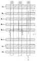
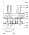
도 1은 본 발명에 따른 유전막을 형성하기에 적합한 증착 반응기를 나타낸다.1 shows a deposition reactor suitable for forming a dielectric film according to the present invention.
도 1을 참조하면, 복수의 기판(W)을 수용하기 위한 공간이 마련되고, 증착 공정이 수행되는 반응 챔버(10)가 구비된다. 상기 반응 챔버(10)는 하단부가 매니폴더 및 시일 캡에 의해 공기가 통하지 않게 밀폐되어 있다.Referring to FIG. 1, a space for accommodating a plurality of substrates W is provided, and a
시일 캡(14)을 통해 기판(W)을 로딩하기 위한 보우트(12)가 삽입되고, 상기 보우트(12)는 상기 반응 챔버(10) 내부에 위치하게 된다. 상기 보우트(12)에는 배치(batch) 처리되는 복수의 기판(W)이 적재된다.A
히터(16)는 반응 챔버(10) 내에 삽입된 기판(W)들을 가열한다. 상기 히터(16)는 상기 반응 챔버(10) 외측에 구비될 수 있다.The
상기 반응 챔버(10) 내에는 적어도 하나의 가스 공급 노즐(18)이 구비되어 있다. 상기 가스 공급 노즐(18)에는 복수의 가스 공급용 홀(도시안함)들이 포함되어 있으며, 상기 가스 공급용 홀들로부터 가스들이 상기 반응 챔버(10)로 공급된다.At least one
상기 가스 공급 노즐(18)과 연결되어 외부로부터 상기 가스가 공급되는 가스 공급관들(20a, 20b, 20c, 24)이 구비된다. 상기 가스 공급관(20a, 20b, 20c, 24)은 공급되는 가스의 종류에 따라 복수개가 구비될 수 있다. 상기 가스 공급관(20a, 20b, 20c, 24)은 매니폴드의 하부를 관통하여 설치된다. 상기 가스 공급관들(20a, 20b, 20b, 24)에는 유량 제어 부재 및 개폐 밸브가 구비될 수 있다.
일 예로, 알루미늄 소오스 가스가 플로우되는 제1 가스 공급관(20a)이 구비된다. 상기 알루미늄 소오스 가스를 희석하기 위한 희석 가스가 플로우되는 제2 가스 공급관(20b)이 구비된다. 상기 제2 가스 공급관(20b)의 일 단부는 상기 제1 가스 공급관(20a)과 연결되어 있다. 즉, 상기 제2 가스 공급관(20b)은 상기 제1 가스 공급관(20a)으로부터 분기된 형상을 갖는다.For example, the first
산소 소오스 가스가 플로우되는 제3 가스 공급관(20c)이 구비된다. 또한, 액체 상태의 알루미늄 소오스를 버블링시켜 기화시키기 위한 케리어 가스가 플로우되는 케리어 가스 공급관(24)이 구비된다.A third
상기 제1 가스 공급관(20a)에는 유량 제어를 위한 제1 매스플로우 컨트롤러 (도시안됨), 제1 개폐 밸브(도시안됨)가 구비될 수 있다.The first
상기 제1 가스 공급관(20a)은 알루미늄 소오스가 채워져 있는 알루미늄 소오스 용기(22)와 연결된다.The first
상기 알루미늄 소오스 용기(22)에는 상기 케리어 가스를 공급하는 케리어 가스 공급관(24)이 연결된다. 상기 알루미늄 소오스 용기(22)에 공급된 알루미늄 소오스는 상온에서 액체 상태이므로, 상기 케리어 가스를 상기 알루미늄 소오스 용기(22) 중에 통과시켜 상기 액체 상태의 알루미늄 소오스를 기화시킨다.The carrier
상기 제2 가스 공급관(20b)은 희석 가스 공급부(28)와 연결된다. 따라서, 상기 제2 가스 공급관(20b)으로 플로우되는 희석 가스는 상기 제1 가스 공급관(20a) 내부로 들어가게 된다. 그러므로, 상기 알루미늄 소오스 가스는 상기 희석 가스에 의해 희석된 상태로 상기 제1 가스 공급관(20a)을 통해 상기 반응 챔버(10) 내부로 제공된다.The second
또한, 상기 제3 가스 공급관(20c)에는 유량 제어를 위한 제2 매스플로우 컨트롤러(도시안됨) 및 제2 개폐 밸브(도시안됨)가 구비될 수 있다. 상기 제3 가스 공급관(20c)에는 적어도 하나의 산소 소오스 가스 발생기가 연결된다. 상기 산소 소오스 가스 발생기는 오존 발생기일 수 있다. 구체적으로, 고농도의 오존을 다량으로 공급하기 위하여, 도시된 것과 같이, 상기 제3 가스 공급관(20c)에 복수개의 오존 발생기(26)가 연결될 수도 있다. 그러나, 이와는 달리, 상기 제3 가스 공급관(20c)에는 1개의 오존 발생기(26)가 연결될 수도 있다.In addition, the third
상기 반응 챔버(10)에는 가스를 배기하는 배기관인 가스 배기관(30)이 연결 되고, 밸브(32)를 통해 배기 수단인 진공 펌프(34)에 접속된다.The
실시예 1Example 1
도 2는 발명의 실시예 1에 따른 알루미늄 산화막을 형성하는 방법을 나타낸다.2 shows a method of forming an aluminum oxide film according to Example 1 of the invention.
이하에서는, 도 1의 증착 반응기를 참조하여 알루미늄 산화막을 형성하는 방법을 설명한다.Hereinafter, a method of forming an aluminum oxide film will be described with reference to the deposition reactor of FIG. 1.
도 2를 참조하면, 배치식 증착 반응기의 반응 챔버(10) 내에 복수의 기판(W)을 로딩한다. 상기 기판(W)들은 서로 이격되면서 보우트(12) 내에 적재되어 있다.Referring to FIG. 2, a plurality of substrates W are loaded into the
상기 반응 챔버(10) 내부에 로딩된 기판(W)은 450 내지 700℃의 온도가 되도록 한다.The substrate W loaded in the
상기 기판(W)들 상에 알루미늄 산화막을 형성하는 공정 시에 상기 기판(W)들의 온도가 450℃보다 낮으면, 형성되는 알루미늄 산화막 내에 불순물이 증가하게 된다. 또한, 막의 치밀도가 감소하게 되어 열을 가했을 때 막이 과도하게 수축되며, 습식 식각 공정을 수행하였을 때 식각율이 증가될 뿐 아니라 식각율의 산포가 커지게 된다. 더구나, 상기 알루미늄 산화막은 트랩이 증가하며, 누설 전류가 증가하게 된다. 반면에, 상기 증착 공정에서 기판들의 온도가 700℃보다 높으면, 알루미늄 소오스 가스가 분해되는 것을 억제할 수 없어 바람직하지 않다. 그러므로, 상기 증착 공정을 수행할 때 상기 반응 챔버 내의 기판들은 450 내지 700℃의 온도가 되도록 한다.When the temperature of the substrates W is lower than 450 ° C. in the process of forming the aluminum oxide layers on the substrates W, impurities may increase in the formed aluminum oxide layers. In addition, as the density of the film decreases, the film is excessively contracted when heat is applied, and when the wet etching process is performed, the etching rate is increased and the spread of the etching rate is increased. Moreover, the aluminum oxide film has an increased trap and an increased leakage current. On the other hand, if the temperature of the substrates in the deposition process is higher than 700 ℃, it is not preferable because it can not suppress the decomposition of the aluminum source gas. Therefore, when performing the deposition process, the substrates in the reaction chamber are brought to a temperature of 450 to 700 ° C.
제1 단계로, 액체 상태의 알루미늄 소오스가 수용되어 있는 알루미늄 소오스 용기(22) 내에 케리어 가스를 유입시키고, 상기 캐리어 가스를 통해 알루미늄 소오스를 기화시킨다. 그리고, 상기 기화된 알루미늄 소오스를 상기 캐리어 가스와 함께 상기 반응 챔버(10) 내부로 이동시킨다. 상기 알루미늄 소오스 가스는 상기 제1 가스 공급관(20a)을 통해 상기 반응 챔버 내부로 이동하게 된다.In a first step, a carrier gas is introduced into an
사용할 수 있는 상기 알루미늄 소오스의 예로는 트리메틸 알루미늄 (trimethyl aluminium, Al(CH3)3), 트리에틸 알루미늄(triethyl aluminium, Al(C2H6)3), 트리이소부틸 알루미늄(triisobutyl aluminium, Al[(C2H3(CH3)2]3) 및 염화 디에틸알루미늄(diethyl aluminium chloride, AlCl(C2H6)3) 등을 들 수 있다. 상기 물질들은 단독으로 또는 상기 물질들의 혼합으로 사용될 수 있다. 상기 알루미늄 소오스는 트리메틸 알루미늄(TMA)을 사용하는 것이 바람직하며, 이하에서는 상기 트리메틸 알루미늄(TMA)을 적용하여 설명한다.Examples of the aluminum source that can be used include trimethyl aluminum (Al (CH3 )3 ), triethyl aluminum, Al (C2 H6 )3 ), triisobutyl aluminum, Al [ (C2 H3 (CH3 )2 ]3 ) and diethyl aluminum chloride (AlCl (C2 H6 )3 ), etc. The materials may be used alone or in combination of the above materials. The aluminum source is preferably trimethyl aluminum (TMA), and will be described below by applying the trimethyl aluminum (TMA).
또한, 상기 알루미늄 소오스 가스와 함께 상기 희석 가스를 상기 반응 챔버(10) 내부로 유입시킨다. 상기 희석 가스는 불활성 가스를 포함한다. 일 예로, 상기 희석 가스는 질소, 아르곤 및 핼륨으로 이루어지는 군에서 선택된 적어도 하나를 포함할 수 있다.In addition, the diluent gas is introduced into the
상기 희석 가스는 제2 가스 공급관(20b)을 통해 상기 제1 가스 공급관(20a)으로 들어가게 되고, 상기 제1 가스 공급관(20a) 내부에 플로우되는 상기 알루미늄 소오스 가스를 희석시킨다. 상기 제1 가스 공급관(20a) 내부에서 희석된 알루미늄 소오스 가스는 상기 반응 챔버(10) 내부에 유입된다. 이와같이, 상기 희석된 알루미늄 소오스 가스는 동일한 공급관을 통해 상기 반응 챔버 내부(10)로 유입된다.The dilution gas enters the first
본 실시예와는 달리 일반적인 방법으로, 상기 가스 공급관을 통해 상기 반응 챔버에 상기 알루미늄 소오스 가스만을 유입하는 경우에는 상기 증착 온도인 450 내지 700℃의 온도에서 상기 알루미늄 소오스 가스가 쉽게 분해된다. 그러므로, 상기 제1 가스 공급관(20a), 반응 챔버(10) 및 보우트(12)에 알루미늄이 부착되어 상기 제1 가스 공급관(20a), 반응 챔버(10) 및 보우트(12)가 오염된다. 또한, 상기 알루미늄 소오스 가스가 분해됨으로써, 상기 반응 챔버(10) 내의 각 기판(W)에 형성되는 박막들의 두께 산포가 매우 커지게 된다.Unlike the present embodiment, when only the aluminum source gas is introduced into the reaction chamber through the gas supply pipe, the aluminum source gas is easily decomposed at the deposition temperature of 450 to 700 ° C. Therefore, aluminum is attached to the first
그러나, 본 실시예에서와 같이, 상기 알루미늄 소오스 가스와 희석 가스를 동일 가스 공급관을 통해 유입시키는 경우, 상기 450 내지 700℃의 온도에서도 상기 알루미늄 소오스 가스의 분해가 억제된다.However, as in the present embodiment, when the aluminum source gas and the dilution gas are introduced through the same gas supply pipe, decomposition of the aluminum source gas is suppressed even at the temperature of 450 to 700 ° C.
구체적으로, 상기 알루미늄 소오스 가스와 함께 상기 알루미늄 소오스 가스의 5배 이상의 유량으로 희석 가스를 유입하면, 상기 450 내지 700℃의 온도에서도 상기 알루미늄 소오스 가스의 분해가 억제된다. 상기 알루미늄 소오스 가스와 함께 희석 가스가 유입되면, 상기 알루미늄 소오스 가스의 유속이 증가된다. 반면에, 전체 유입 가스에서 상기 알루미늄 소오스 가스의 농도는 상대적으로 감소된다. 따라서, 상기 450 내지 700℃의 고온에서도 상기 알루미늄 소오스 가스의 분해가 억제되는 것이다.Specifically, when the diluent gas is introduced at a flow rate of five times or more of the aluminum source gas together with the aluminum source gas, decomposition of the aluminum source gas is suppressed even at the temperature of 450 to 700 ° C. When a dilution gas is introduced together with the aluminum source gas, the flow rate of the aluminum source gas is increased. On the other hand, the concentration of the aluminum source gas in the total incoming gas is relatively reduced. Therefore, decomposition of the aluminum source gas is suppressed even at the high temperature of 450 to 700 ° C.
상기 알루미늄 소오스 가스의 분해를 억제시키기 위해서는 상기 희석 가스의 유입량을 증가시키는 것이 바람직하다. 그러나, 상기 희석 가스가 상기 알루미늄 소오스 가스의 80배 이상이 되는 경우에는 상대적으로 알루미늄 소오스 가스의 양이 감소되어 알루미늄 산화막의 증착 속도가 지나치게 느려질 수 있다. 그러므로, 상기 알루미늄 소오스 가스 및 희석 가스의 비는 1: 5 내지 80인 것이 바람직하다.In order to suppress decomposition of the aluminum source gas, it is preferable to increase the inflow amount of the diluent gas. However, when the dilution gas is 80 times or more than the aluminum source gas, the amount of aluminum source gas may be relatively reduced, and the deposition rate of the aluminum oxide film may be too slow. Therefore, the ratio of the aluminum source gas and the dilution gas is preferably 1: 5 to 80.
제2 단계로, 상기 알루미늄 소오스 가스를 퍼지한다. 즉, 상기 알루미늄 소오스 가스의 유입을 중단시킨 다음, 상기 반응 챔버 내부에 알루미늄 소오스 가스를 퍼지하기 위한 퍼지 가스를 유입시킨다. 상기 퍼지 가스는 불활성 가스를 포함한다.In a second step, the aluminum source gas is purged. That is, after the inflow of the aluminum source gas is stopped, a purge gas for purging the aluminum source gas is introduced into the reaction chamber. The purge gas includes an inert gas.
제3 단계로, 상기 반응 챔버(10) 내부에 로딩된 기판으로 산소 소오스 가스를 유입한다. 상기 산소 소오스 가스는 오존, H2O 등을 들 수 있다. 본 실시예에서 상기 소오스 가스는 오존을 사용하며, 상기 제3 가스 공급관(20c)으로부터 오존 가스를 유입시킨다.In a third step, the oxygen source gas is introduced into the substrate loaded in the
또한, 상기 오존 가스는 350g/㎤의 농도를 가지면서 10slm(Standard Liter per Minute)이상의 유량으로 유입시키는 것이 바람직하다. 즉, 본 실시예에서는 증착 공정을 통해 형성된 알루미늄 산화막 내에 산화물이 결합되지 않은 빈공간(vacancy)이 감소되도록 하기 위하여, 상기 오존 가스의 유입량 및 오존 가스의 농도를 증가시킨다. 이를 위하여, 도 1에 도시된 것과 같이, 상기 알루미늄 산화막을 형성하기 위한 증착 설비에는 복수개의 오존 생성기가 연결되어 있을 수 있다.In addition, the ozone gas is preferably introduced at a flow rate of 10 slm (Standard Liter per Minute) or more while having a concentration of 350 g /
상기 오존 가스는 상기 기판 상에 흡착되어 있는 알루미늄 소오스 가스와 반 응한다. 이로써, 상기 기판 상에는 알루미늄 산화 박막(Al2O3)이 형성된다.The ozone gas reacts with the aluminum source gas adsorbed on the substrate. As a result, an aluminum oxide thin film (Al2 O3 ) is formed on the substrate.
설명한 것과 같이, 상기 알루미늄 산화 박막은 450 내지 700℃의 고온에서 형성된다. 그러므로, 상기 고온에서 형성된 알루미늄 산화막은 400℃ 이하의 낮은 온도에서 형성되는 알루미늄 산화막에 비해 불순물이 감소되고, 높은 밀도를 가지며, 누설 전류 특성도 양호하다.As described, the aluminum oxide thin film is formed at a high temperature of 450 to 700 ℃. Therefore, the aluminum oxide film formed at the high temperature has less impurities, higher density, and better leakage current characteristics than the aluminum oxide film formed at a low temperature of 400 ° C. or lower.
제4 단계로, 상기 산소 소오스 가스를 퍼지한다. 즉, 상기 오존 가스의 유입을 중단시킨 다음, 상기 반응 챔버(10) 내부에 오존 가스를 퍼지하기 위한 퍼지 가스를 유입시킨다. 상기 퍼지 가스는 불활성 가스를 포함한다.In a fourth step, the oxygen source gas is purged. That is, after the inflow of the ozone gas is stopped, a purge gas for purging the ozone gas is introduced into the
상기 설명한 1 내지 4단계를 하나의 싸이클로 하고, 상기 싸이클을 복수회 반복함으로써 상기 기판 상에 원하는 두께의 알루미늄 산화막을 형성한다.
상기 공정을 통해 형성된 알루미늄 산화막은 인-웨이퍼 두께(In-Wafer thickness) 산포가 1% 이내가 된다. 즉, 각각의 기판 상에 형성된 알루미늄 산화막은 각 기판 표면의 위치별로 두께 산포가 1% 이내가 된다. 또한, 상기 공정을 통해 형성된 알루미늄 산화막은 웨이퍼간 두께(wafer to wafer thickness) 산포가 1% 이내가 된다. 즉, 상기 반응 챔버 내의 복수의 기판에 형성된 각 알루미늄 산화막은 두께의 산포가 1% 이내가 된다. 이와같이, 동일한 챔버 내에서 형성된 기판들에 형성된 알루미늄 산화막의 두께 산포 및 각 기판 내에 형성된 알루미늄 산화막의 두께 산포가 모두 낮다. 그러므로, 균일한 두께를 갖는 알루미늄 산화막을 형성할 수 있다.The aluminum oxide film formed through the process has an in-wafer thickness distribution within 1%. In other words, the aluminum oxide film formed on each substrate has a thickness variation of less than 1% for each position of each substrate surface. In addition, the aluminum oxide film formed through the above process has a dispersion of wafer to wafer thickness within 1%. That is, each aluminum oxide film formed on the plurality of substrates in the reaction chamber has a dispersion of less than 1% in thickness. As such, both the thickness distribution of the aluminum oxide film formed on the substrates formed in the same chamber and the thickness distribution of the aluminum oxide film formed in each substrate are low. Therefore, an aluminum oxide film having a uniform thickness can be formed.
상기 공정을 통해 형성된 알루미늄 산화막은 막의 밀도가 치밀하고 불순물의 함량이 작으므로, 막의 수축 및 식각율의 특성이 양호하다. 이에 더하여, 상기 알루미늄 산화막은 막 내의 수소의 함량이 감소되므로 트랩 특성, 누설 전류 특성 및 밴드갭 특성이 양호하다.Since the aluminum oxide film formed through the process has a dense film and a small content of impurities, the film has good characteristics of shrinkage and etching rate. In addition, since the content of hydrogen in the film is reduced, the aluminum oxide film has good trap characteristics, leakage current characteristics, and band gap characteristics.
이하에서는, 도 2를 참조로 설명한 알루미늄 산화막을 포함하는 플래시 메모리 소자 및 그 제조 방법에 대해 설명한다.Hereinafter, a flash memory device including the aluminum oxide film described with reference to FIG. 2 and a manufacturing method thereof will be described.
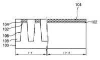
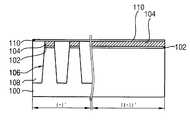
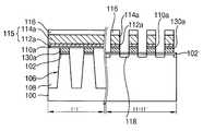
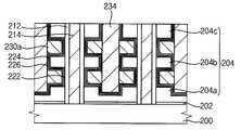
도 3은 도 1에 도시한 알루미늄 산화막을 포함하는 플래시 메모리 소자의 평면도이다. 도 4는 도 3에 도시한 플래시 메모리 소자의 단면도이다. 도 4는 도 3에서 I-I' 라인 및 II-II' 라인을 따라 절단된 단면들을 도시한다.3 is a plan view of a flash memory device including the aluminum oxide film shown in FIG. 1. 4 is a cross-sectional view of the flash memory device shown in FIG. 3. 4 shows cross-sections cut along the lines II ′ and II-II ′ in FIG. 3.
도 3 및 4를 참조하면, 소자 분리막 패턴(108)이 형성된 기판(100)이 마련된다. 상기 소자 분리막 패턴에 의해 정의된 액티브 영역은 제1 방향으로 연장되는 라인 형상을 갖는다.3 and 4, the
상기 기판(100) 상에 터널 산화막(102), 플로팅 게이트 패턴(104a)이 적층된다. 상기 터널 산화막(102)은 실리콘 산화물을 포함할 수 있다. 상기 플로팅 게이트 패턴(104a)은 불순물이 도핑된 폴리실리콘으로 이루어질 수 있다.The
상기 플로팅 게이트 패턴(104a) 및 소자 분리막 패턴(108) 상에 유전막 패턴(110a)이 구비된다. 상기 유전막 패턴(110a)은 상기 소자 분리막 패턴(108)과 수직하게 배치되는 라인 형상을 갖는다. 상기 유전막 패턴(110a)은 알루미늄 산화물로 이루어진다. 상기 알루미늄 산화물은 실시예 1의 방법에 의해 형성된 것이다. 즉, 상기 알루미늄 산화물은 산화물 베이컨시가 감소되어 높은 밀도를 가지고, 불순물로 인한 트랩이 작다. 이와같이, 플래시 메모리 소자에 고유전율을 가지면서도 높은 및도 및 낮은 불순물을 갖는 유전막 패턴이 포함됨으로써, 상기 플래시 메모리 소자는 누설 전류가 낮아지고 및 신뢰성이 높아진다.A
상기 유전막 패턴(110a) 상에, 금속막 패턴(112a) 및 폴리실리콘 패턴(114a)이 적층된 콘트롤 게이트 패턴(115)이 구비된다. 상기 금속막 패턴(112a)으로 사용되는 물질의 예로는 티타늄, 티타늄 질화물, 탄탄륨, 탄탈륨 질화물 등을 들 수 있다. 이들은 단독 또는 2 이상이 적층될 수 있다. 상기 콘트롤 게이트 패턴(115)은 워드 라인으로 제공된다. 상기 콘트롤 게이트 패턴(115)은 상기 제1 방향과 수직한 제2 방향으로 연장되는 라인 형상을 갖는다.On the
상기 콘트롤 게이트 패턴(115) 상에는 하드 마스크 패턴(116)이 구비된다.The
상기 터널 산화막(102), 플로팅 게이트 패턴(104a), 유전막 패턴(110a), 콘트롤 게이트 패턴(115) 및 하드 마스크 패턴(116)이 적층된 게이트 구조물들 사이의 기판(100) 아래는 불순물 영역(118)이 구비된다.An impurity region may be formed under the
또한, 도 3에 도시된 것과 같이, 셀을 선택하기 위한 선택 트랜지스터들이 구비될 수 있다. 상기 선택 트랜지스터의 게이트 전극은 각각 소오스 선택 라인(SSL) 및 접지 선택 라인(GSL)으로 제공된다. 또한, 비트 라인 및 공통 소스 라인(CSL)이 구비된다.In addition, as illustrated in FIG. 3, select transistors for selecting a cell may be provided. The gate electrode of the select transistor is provided to the source select line SSL and the ground select line GSL, respectively. In addition, a bit line and a common source line CSL are provided.
도 5 내지 도 8은 도 3 및 도 4에 도시된 플래시 메모리 소자의 제조 방법을 설명하기 위한 단면도들이다.5 to 8 are cross-sectional views illustrating a method of manufacturing the flash memory device illustrated in FIGS. 3 and 4.
도 5 내지 도 8은 도 3에서 I-I' 라인 및 II-II' 라인을 따라 절단된 단면들을 도시한다.5 to 8 show cross sections cut along the lines II ′ and II-II ′ in FIG. 3.
도 5를 참조하면, 기판(100) 상에 터널 산화막(102) 및 플로팅 게이트막(도시안됨)을 순차적으로 형성한다. 상기 기판(100)은 실리콘(silicon) 또는 게르마늄(germanium)을 포함하는 반도체 기판일 수 있다. 상기 터널 산화막(102)은 기판의 표면 부위를 열 산화시키는 열 산화(thermal oxidation) 공정을 이용하여 형성될 수 있다. 상기 플로팅 게이트막은 폴리실리콘막을 증착하여 형성할 수 있다.Referring to FIG. 5, a
상기 플로팅 게이트막 상에 제1 하드 마스크 패턴(도시안됨)을 형성한다. 상기 제1 하드 마스크 패턴을 식각 마스크로 이용하여, 상기 플로팅 게이트막, 터널 산화막(102) 및 기판(100)을 식각한다. 상기 공정을 통해, 예비 플로팅 게이트 패턴(104)이 형성된다. 또한, 소자 분리 영역의 기판(100)에 트렌치(106)가 형성된다.A first hard mask pattern (not shown) is formed on the floating gate layer. The floating gate layer, the
상기 트렌치(106) 내부 및 상기 예비 플로팅 게이트 패턴(104) 사이를 채우는 절연막을 형성하고, 이를 연마함으로써, 소자 분리막 패턴(108)을 형성한다. 다음에, 상기 제1 하드 마스크 패턴을 제거한다. 도시하지는 않았지만, 선택적으로, 상기 예비 플로팅 게이트 패턴(104)의 측벽 일부가 노출되도록 상기 소자 분리막 패턴(108)의 상부를 일부 제거할 수도 있다.An insulating layer filling the inside of the
도 6을 참조하면, 상기 예비 플로팅 게이트 패턴(104) 및 소자 분리막 패턴(108) 상에 블록킹 유전막으로 제공되기 위한 알루미늄 산화막(110)을 형성한다.Referring to FIG. 6, an
상기 블록킹 유전막은 얇은 등가 산화막 두께(EOT)를 유지할 수 있도록 고유전율을 갖는 것이 바람직하다. 또한, 상기 블록킹 유전막은 고밀도를 가지면서 트랩이 감소되어, 상기 블록킹 유전막으로부터 누설 전류가 발생되지 않는 것이 바람직하다.The blocking dielectric layer preferably has a high dielectric constant to maintain a thin equivalent oxide film thickness (EOT). In addition, it is preferable that the blocking dielectric layer has a high density and a trap is reduced, so that no leakage current is generated from the blocking dielectric layer.
본 실시예에서, 상기 실시예 1의 알루미늄 산화막의 형성 공정과 동일한 공정을 수행함으로써 블록킹 유전막으로 제공되는 알루미늄 산화막(110)을 형성한다. 상기 공정을 통해 형성되는 알루미늄 산화막(110)은 막 내의 수소 함량이 작아서 트랩 특성, 누설 전류 특성 및 밴드갭 특성이 양호하다. 또한, 상기 알루미늄 산화막(110)은 밀도가 높아서 치밀한 구조를 갖는다.In this embodiment, the
상기 알루미늄 산화막(110)을 형성한 후에 상기 알루미늄 산화막(110)을 열처리하여 알루미늄 산화막(110) 내의 결정 결함들을 치유한다. 상기 열처리는 700 내지 1000℃의 고온으로 진행될 수 있다. 상기 열처리 공정은 자외선 오존(UV-O3) 처리, 플라즈마 처리 등을 포함할 수 있다.After the
도시하지는 않았지만, 플래시 메모리 소자에서 선택 트랜지스터가 형성될 부위의 알루미늄 산화막(110)을 제거하는 버팅(butting) 공정을 더 수행한다. 따라서, 상기 알루미늄 산화막(110)이 제거된 부위는 후속 공정을 통해 셀 스트링을 선택하기 위한 스위치 기능을 하는 MOS 트랜지스터로 제공된다.Although not shown, a butting process of removing the
도 7을 참조하면, 상기 알루미늄 산화막(110) 상에 금속막(112)을 형성한다. 상기 금속막(112)은 티타늄, 티타늄 질화물, 탄탈륨, 탄탈륨 질화물 등으로 형성할 수 있으며, 이들은 단독으로 형성되거나 2층 이상으로 적층시켜 형성할 수도 있다. 상기 금속막(112)은 패터닝하기가 용이하지 않으므로 1000Å이하의 낮은 두께로 형성하는 것이 바람직하다. 상기 금속막(112) 상에 불순물이 도핑된 폴리실리콘막(114)을 형성한다. 상기 금속막(112) 및 폴리실리콘막(114)은 후속 공정을 통해 콘트롤 게이트 패턴으로 제공된다.Referring to FIG. 7, a
도 8을 참조하면, 상기 폴리실리콘막(114) 상에 하드 마스크 패턴(116)을 형성한다. 이 후, 상기 폴리실리콘막(114), 금속막(112), 알루미늄 산화막(110), 예비 플로팅 게이트 패턴(104)을 순차적으로 식각하여 게이트 구조물을 형성한다. 상기 게이트 구조물에는 터널 산화막(102), 고립된 패턴 형상을 갖는 플로팅 게이트 패턴(104a), 상기 플로팅 게이트 패턴(104a) 상에 형성되고 알루미늄 산화물로 이루어지는 유전막 패턴(110a), 라인 형상을 갖는 콘트롤 게이트 패턴(115) 및 하드 마스크 패턴(116)이 포함된다. 상기 콘트롤 게이트 패턴(115)은 금속 및 폴리실리콘이 적층된 형상을 갖는다.Referring to FIG. 8, a
상기 게이트 구조물 사이의 기판(100) 표면 아래로 불순물을 주입하여 불순물 영역(118)을 형성한다.An
상기 공정을 수행하면, 고유전율을 가지고, 고밀도를 가지면서 불순물의 함량이 작은 알루미늄 산화물을 포함하는 플래시 메모리 소자를 제조할 수 있다. 따라서, 상기 플래시 메모리 소자는 우수한 전기적 특성을 갖는다.By performing the above process, a flash memory device having a high dielectric constant, a high density, and a small content of impurities may be manufactured. Thus, the flash memory device has excellent electrical characteristics.
실시예 2Example 2
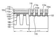
도 9는 본 발명의 실시예 2에 따른 플래시 메모리 소자를 나타낸다. 이하에서 설명하는 본 실시예의 플래시 메모리 소자는 실시예 1의 방법으로 형성된 알루미늄 산화막이 포함된다. 또한, 본 실시예의 메모리 소자는 전하를 저장하기 위한 패턴으로써, 전하 트랩막 패턴을 사용하는 것을 제외하고는 실시예 1의 플래시 메모리 소자와 동일한 구성을 갖는다.9 shows a flash memory device according to
도 9를 참조하면, 소자 분리막 패턴(도시안됨)이 형성된 기판(100)이 마련된다. 상기 기판(100)상에 터널 산화막(102), 전하 트랩막 패턴(130a) 및 유전막 패턴(110a)이 적층된다.9, a
상기 전하 트랩막 패턴(130a)은 실리콘 질화물로 이루어질 수 있다. 이와는 달리, 상기 전하 트랩막 패턴(130a)은 금속 산화물로 이루어질 수도 있다.The charge
상기 유전막 패턴(110a)은 실시예 1의 방법에 의해 형성된 알루미늄 산화물로 이루어진다. 상기 알루미늄 산화물로 이루어지는 유전막 패턴(110a)은 높은 밀도를 가지고, 불순물 함량이 작으며, 트랩이 감소된다.The
상기 유전막 패턴(110a) 상에, 금속막 패턴(112a) 및 폴리실리콘 패턴(114a)이 적층된 콘트롤 게이트 패턴(115)이 구비된다. 상기 콘트롤 게이트 패턴(115) 상에는 하드 마스크 패턴(116)이 구비된다. 상기 터널 산화막(102), 플로팅 게이트 패턴(104a), 유전막 패턴(110a), 콘트롤 게이트 패턴(115)이 적층된 게이트 구조물들 사이의 기판 아래는 불순물 영역(118)이 구비된다.On the
상기 실시예 2에 따른 비휘발성 메모리 소자는 전하 저장막으로써 플로팅 게이트막 대신에 전하 트랩막을 형성하는 것을 제외하고는 도 5 내지 도 8을 참조로 설명한 것과 동일하게 진행하여 제조될 수 있다.The nonvolatile memory device according to the second embodiment may be manufactured in the same manner as described with reference to FIGS. 5 to 8 except that a charge trap layer is formed instead of the floating gate layer as the charge storage layer.
실시예 3Example 3
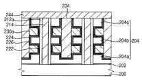
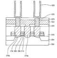
도 10a는 본 발명의 실시예 3에 따른 수직형 NAND 플래시 메모리 소자를 나타내는 사시도이다. 도 10b는 도 10a에 도시된 수직형 NAND 플래시 메모리 소자를 나타내는 단면도이다.10A is a perspective view illustrating a vertical NAND flash memory device according to
본 실시예의 수직형 NAND 플래시 메모리 소자는 도 1을 참조로 설명한 것과 동일한 공정을 통해 수득된 알루미늄 산화막이 포함된다.The vertical NAND flash memory device of this embodiment includes an aluminum oxide film obtained through the same process as described with reference to FIG.
도 10a 및 도 10b를 참조하면, 단결정 반도체 물질로 이루어지는 기판(200)이 구비된다. 상기 기판(200) 표면 아래에는 공통 소오스 라인으로 제공되는 불순물 영역(도시안됨)이 구비된다. 상기 불순물 영역이 구비됨으로써, 상기 단결정 반도체 패턴(212a)들에 형성되어 있는 각 셀 스트링들의 하부가 서로 연결된다.10A and 10B, a
상기 기판(200) 상에는 패드 산화막(202)이 구비된다. 상기 기판(200) 상에는 제1 방향으로 연장되는 라인 형상의 절연막 패턴들(214)이 구비된다. 상기 라인 형상의 절연막 패턴(214)은 기판 표면으로부터 수직하게 배치된다.The
상기 절연막 패턴(214)의 양 측벽에는 필러 형상의 단결정 반도체 패턴(212a)들이 구비된다. 상기 단결정 반도체 패턴(212a)들은 수직에 가까운 측벽 경사를 갖는다. 상기 단결정 반도체 패턴(212a)은 직육면체의 필러 형상을 가지면서 규칙적으로 배치된다.Filler-shaped single
상기 단결정 반도체 패턴(212a)에서 상기 절연막 패턴(214)과 접하는 측벽 (이하, 제1 측벽)과 마주하는 다른 측벽(이하, 제2 측벽)에는 플래시 메모리 소자의 셀들을 이루는 셀 트랜지스터들이 구비된다. 상기 필러 형상의 단결정 반도체 패턴(212a)에는 수직방향으로 직렬 연결된 셀 트랜지스터들이 구비되고, 상기 셀 트랜지스터들은 하나의 셀 스트링을 이룬다.In the single
상기 단결정 반도체 패턴(212a)들의 제2 측벽과 접촉하는 층간 절연막 패턴(204)들이 구비된다. 상기 층간 절연막 패턴(204)들은 서로 일정 간격 이격되도록 배치되고, 제1 방향으로 연장되는 라인 형상을 갖는다.Interlayer insulating
상기 층간 절연막 패턴(204)들 사이의 갭 부위에는 상기 셀 트랜지스터들이 구비된다. 이하에서는, 상기 단결정 반도체 패턴(212a)에 형성되는 셀 트랜지스터에 대해 보다 상세하게 설명한다.The cell transistors are provided in the gap region between the interlayer insulating
상기 단결정 반도체 패턴(212a)들 일 측벽에는 터널 산화막(222)이 구비된다. 상기 터널 산화막(222) 상에는 전하 트랩막(224)들이 구비된다. 상기 전하 트랩막(224)은 전하를 트랩핑할 수 있는 물질인 실리콘 질화물로 이루어질 수 있다.A
상기 전하 트랩막(224) 상에는 블록킹 유전막(226)이 구비된다. 상기 블록킹 유전막(226)은 알루미늄 산화물로 이루어질 수 있다. 상기 알루미늄 산화물은 실시예 1에서 설명한 것과 동일한 공정을 통해 형성된 것 일 수 있다. 상기 알루미늄 산화물은 산화물 베이컨시가 감소되어 높은 밀도를 가지고, 불순물로 인한 트랩이 작다. 이와같이, 수직형 NAND 플래시 메모리 소자에 고유전율을 가지면서도 밀도가 높고 불순물이 거의 없는 블록킹 유전막(226)이 포함됨으로써, 상기 수직형 NAND 플래시 메모리 소자는 누설 전류가 낮아지고 및 신뢰성이 높아진다.A blocking
상기 전하 트랩막(224)과 동일한 층에서 제1 방향으로 배치되는 블록킹 유전막(226)은 수평 방향으로 서로 연결되어 있는 형상을 가질 수 있다. 또한, 도시된 것과 같이, 동일한 단결정 반도체 패턴(212a)에 형성되는 블록킹 유전막(226)은 수직 방향으로도 서로 연결될 수도 있다.The blocking
상기 블록킹 유전막(226) 표면과 접촉하면서 상기 층간 절연막 패턴들 사이의 갭 부위에 콘트롤 게이트 패턴(230a)들이 구비된다. 동일한 층에서 제1 방향으로 배치되는 상기 콘트롤 게이트 패턴(230a)들은 라인 형상을 갖는다. 때문에, 상기 각각의 콘트롤 게이트 패턴(230a)은 워드 라인으로 제공된다.
또한, 상기 층간 절연막 패턴들(204) 및 상기 콘트롤 게이트 패턴(230a)들의 사이에는 실리콘 산화막 패턴(242)이 구비된다.In addition, a silicon
상기 제1 방향으로 배치된 상기 단결정 반도체 패턴(212a)들의 상부면을 전기적으로 연결시키는 비트 라인(244)이 구비된다.The
도시되지는 않았지만, 본 발명의 일 실시예에서 상기 단결정 반도체 패턴(212a)의 최 상부 및 최 하부의 각 측벽에는 게이트 절연막 패턴 및 게이트 전극이 구비된 상, 하부 선택 트랜지스터가 구비될 수도 있다.Although not shown, top and bottom sidewalls of the single
본 실시예에 따른 수직형 NAND 플래시 메모리 소자는 고유전율을 가지고, 고밀도를 가지면서 불순물의 함량이 작은 알루미늄 산화물을 포함한다. 따라서, 상기 수직형 NAND 플래시 메모리 소자는 우수한 전기적 특성을 갖는다.The vertical NAND flash memory device according to the present exemplary embodiment includes aluminum oxide having high dielectric constant, high density, and low content of impurities. Thus, the vertical NAND flash memory device has excellent electrical characteristics.
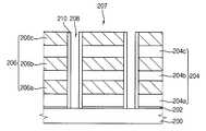
도 11 내지 도 19는 도 10a 및 도 10b에 도시된 수직형 NAND 플래시 메모리 소자의 제조 방법을 나타내는 단면도이다.11 to 19 are cross-sectional views illustrating a method of manufacturing the vertical NAND flash memory device illustrated in FIGS. 10A and 10B.
도 17은 도 16의 일부 영역을 확대 도시한 것이다.17 is an enlarged view of a portion of FIG. 16.
도 11을 참조하면, 단결정 실리콘으로 이루진 기판(200)을 마련한다. 상기 기판(200)의 일부 영역에 N형의 불순물을 도핑함으로써, NAND 플래시 메모리 소자의 공통 소오스 라인으로 제공되는 불순물 영역(도시안됨)을 형성한다. 상기 기판(200) 상에 패드 산화막(202)을 형성한다. 상기 패드 산화막(202) 상에 층간 절연막 및 희생막을 반복하여 적층한다.Referring to FIG. 11, a
최 상부에 위치하는 희생막 상에 제1 식각 마스크 패턴을 형성하고, 이를 이용하여 상기 희생막들 및 층간 절연막들을 순차적으로 식각함으로써 제1 방향으로 연장되는 형상의 제1 트렌치(208)들을 형성한다. 따라서, 상기 희생막 패턴들(206) 및 층간 절연막 패턴들(204)이 적층되고, 제1 트렌치가 생성되어 있는 절연막 구조물이 형성된다.A first etching mask pattern is formed on the sacrificial layer positioned on the uppermost layer, and the
상기 제1 트렌치(208)들의 측벽, 기판(200) 표면 및 희생막 패턴(206)의 상부면을 따라 비정질 실리콘막(도시안됨)을 형성한다. 이 후, 상기 제1 트렌치(208)의 양 측벽에만 상기 비정질 실리콘막이 남아있도록 상기 비정질 실리콘막을 이방성으로 식각하여 스페이서 형상의 비정질 실리콘 패턴(210)을 형성한다.An amorphous silicon layer (not shown) is formed along the sidewalls of the
도 12를 참조하면, 상기 비정질 실리콘 패턴(210)이 형성되어 있는 제1 트렌치(208) 내부를 채우는 실리콘 산화막 패턴(213)을 형성한다.Referring to FIG. 12, a silicon
다음에, 상기 비정질 실리콘 패턴(210)을 열처리 또는 레이저 빔 조사 등을 통해 상기 비정질 실리콘을 단결정 실리콘으로 상전이시킨다. 따라서, 상기 제1 트 렌치(208) 내부에 예비 단결정 실리콘 패턴(212)을 형성한다.Next, the
도 13을 참조하면, 상기 최상부 층간 절연막 패턴(204c)의 상부면이 노출되도록 상기 실리콘 산화막 패턴(213) 및 예비 단결정 실리콘 패턴(212)의 일부와 최상부 희생막 패턴(206c)을 연마함으로써, 상기 제1 트렌치(208) 내부를 채우는 절연막 패턴(214)을 형성한다. 또한, 상기 공정을 수행함으로써, 예비 단결정 실리콘 패턴(212)의 상부면이 평탄해지게 된다.Referring to FIG. 13, a portion of the silicon
다음에, 상기 최상부 층간 절연막 패턴(204c), 절연막 패턴(214) 및 예비 단결정 실리콘 패턴(212) 상에 캡핑막(216)을 형성한다.Next, a
도 14를 참조하면, 상기 캡핑막(216) 상에 상기 예비 단결정 실리콘 패턴(212) 사이의 절연막 구조물의 일부분을 노출시키는 제2 식각 마스크 패턴(도시안됨)을 형성한다. 다음에, 상기 제2 식각 마스크 패턴을 식각 마스크로 사용하여 상기 캡핑막(216) 및 상기 절연막 구조물의 각 층들을 순차적으로 식각함으로써 제1 개구부(218)를 형성한다.Referring to FIG. 14, a second etching mask pattern (not shown) is formed on the
상기 제1 개구부(218) 측벽에 노출되는 각 층 희생막 패턴(206)들을 습식 식각 공정을 통해 제거함으로써, 제1 개구부(218) 측방과 연통하는 제2 개구부(220)를 형성한다. 상기 제2 개구부(220)의 일부 표면에는 상기 예비 단결정 실리콘 패턴(212)의 측벽이 노출된다.Each layer
상기 공정을 수행하면, 상기 예비 단결정 실리콘 패턴(212)의 일 측벽에는 제1 방향으로 연장되는 층간 절연막 패턴들(204)이 형성된다. 또한, 상기 층간 절연막 패턴들(204) 사이에는 제2 개구부(220)가 생성된다.When the process is performed, interlayer insulating
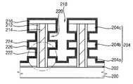
도 15를 참조하면, 상기 노출된 예비 단결정 실리콘 패턴(212)에 터널 산화막(222)을 형성한다. 상기 터널 산화막(222)은 열산화 공정 또는 화학기상 증착법을 통해 형성될 수 있다. 다음에, 상기 터널 산화막(222) 표면을 따라 전하 트랩막(224)을 형성한다. 상기 전하 트랩막(224)은 화학기상증착법으로 형성될 수 있다. 상기 전하 트랩막(224)은 실리콘 질화물 또는 금속 산화물을 증착시켜 형성할 수 있다. 상기 실리콘 질화물 및 금속 산화물은 절연 물질이므로, 서로 연결되어 있더라도 각 셀 트랜지스터들이 서로 전기적으로 쇼트되지 않는다.Referring to FIG. 15, a
도 16 및 도 17을 참조하면, 상기 전하 트랩막(224) 표면 상에 블록킹 유전막(226)을 형성한다. 상기 블록킹 유전막(226)은 알루미늄 산화물을 증착시켜 형성한다. 상기 알루미늄 산화물은 실시예 1에서 설명한 것과 동일한 공정을 통해 형성될 수 있다. 따라서, 상기 블록킹 유전막(226)은 상기 알루미늄 산화물은 산화물 베이컨시가 감소되어 높은 밀도를 가지고, 불순물로 인한 트랩이 작다.16 and 17, a blocking
도 18을 참조하면, 상기 블록킹 유전막(226) 상에, 상기 제1 개구부(218) 및 제2 개구부(220) 내부를 완전히 채우도록 도전막(도시안됨)을 증착한다. 상기 도전막을 증착한 이 후에, 최상부 층간 절연막 패턴(204c)의 상부면이 노출되도록 상기 도전막을 연마함으로써, 상기 제1 개구부(218) 및 제2 개구부(220) 내부에 도전막 패턴(도시안됨)을 형성한다.Referring to FIG. 18, a conductive film (not shown) is deposited on the blocking
상기 결과물의 상부 표면에 상기 제1 개구부(218) 내부에 형성되어 있는 도전막 패턴 상부면을 선택적으로 노출하는 제3 식각 마스크 패턴(도시안됨)을 형성한다. 상기 제3 식각 마스크 패턴을 사용하여 상기 노출된 도전막 패턴(도시안됨) 을 이방성 식각함으로써, 상기 각 층의 도전막 패턴들이 수직 방향으로 서로 분리되도록 하는 제3 개구부(232)를 형성한다. 즉, 상기 제3 개구부(232)는 상기 제1 개구부(218)와 동일한 형상을 갖는다.A third etch mask pattern (not shown) is formed on an upper surface of the resultant material to selectively expose an upper surface of the conductive layer pattern formed in the
상기 공정에 의해, 상기 각 층 층간 절연막 패턴(204) 사이에 수직 방향으로 서로 분리된 콘트롤 게이트 패턴(230a)들이 형성된다. 상기 콘트롤 게이트 패턴(230a)의 상, 하부면 및 일 측벽은 상기 블록킹 유전막(226)과 접하는 형상을 갖는다.By the above process, control
도 19를 참조하면, 상기 제3 개구부(232) 내부에 실리콘 산화막을 증착시키고, 상기 최상부 층간 절연막 패턴(204c)이 노출되도록 상기 실리콘 산화막을 연마함으로써 제1 실리콘 산화막 패턴(234)을 형성한다.Referring to FIG. 19, a silicon oxide film is deposited inside the
이 후에, 도 10a 및 도 10b에 도시된 것과 같이, 상기 예비 단결정 실리콘 패턴(212)의 일부분을 이방성 식각함으로써, 필러 형상의 단결정 반도체 패턴(212a)을 형성한다. 또한, 상기 필러 형상의 단결정 반도체 패턴(212a) 사이의 갭 내에 제2 실리콘 산화막 패턴(242)을 형성한다.Thereafter, as shown in FIGS. 10A and 10B, a portion of the preliminary single
계속하여, 상기 제1 방향으로 배치된 상기 단결정 반도체 패턴(212a)들의 상부면을 전기적으로 연결시키는 비트 라인(244)을 형성한다.Subsequently, a
상기 공정을 수행함으로써, 수직형 NAND 플래시 메모리 소자를 형성할 수 있다.By performing the above process, a vertical NAND flash memory device can be formed.
실시예 4Example 4
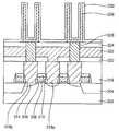
도 20은 본 발명의 실시예 4에 따른 커패시터를 나타낸다.20 shows a capacitor according to
도 20을 참조하면, 기판(250) 상에 하부 전극(252)이 구비된다. 상기 하부 전극(252)은 폴리 실리콘, 티타늄, 티타늄 질화물, 탄탈륨, 탄탈륨 질화물, 텅스텐 질화물, 루테늄 등과 같은 물질로 이루어질 수 있다. 상기 물질은 한 층으로 이루어질 수도 있고, 둘 이상이 적층될 수도 있다.Referring to FIG. 20, a
상기 하부 전극(252) 상에는 유전막 패턴(254)이 구비된다. 상기 유전막 패턴(254)은 실시예 1에서 설명한 방법으로 형성된 알루미늄 산화물로 이루어진다. 상기 알루미늄 산화물로 이루어진 유전막 패턴은 고유전율을 갖는다. 또한, 상기 유전막 패턴은 높은 밀도를 갖고 불순물의 함량이 작다. 때문에, 상기 유전막 패턴을 포함하는 커패시터는 높은 커패시턴스를 가지면서도 누설 전류가 거의 없다.A
상기 유전막 패턴(254) 상에는 상부 전극(259)이 구비된다. 상기 유전막 패턴(254)과 직접 접촉되는 부위의 상부 전극(259)은 금속 패턴(256)으로 이루어지는 것이 바람직하다. 일 예로, 상기 금속 패턴(256)을 이루는 물질은 질화 티타늄, 질화 탄탈륨, 질화 텅스텐, 루데늄 등을 들 수 있다. 또한, 상기 금속 패턴(256) 상에는 폴리실리콘 패턴(258)이 더 구비될 수 있다.An
본 실시예의 커패시터의 하부 전극은 스택 구조를 가지지만, 이와는 달리, 하부 전극이 실린더의 형상을 가질 수도 있다.Although the lower electrode of the capacitor of the present embodiment has a stack structure, the lower electrode may alternatively have the shape of a cylinder.
도 20에 도시된 커패시터는 다음에 설명하는 공정들을 수행함으로써 형성할 수 있다.The capacitor shown in FIG. 20 can be formed by performing the processes described below.
먼저, 기판(250) 상에 하부 전극막을 형성한다. 상기 하부 전극막은 폴리 실리콘, 티타늄, 티타늄 질화물, 탄탈륨, 탄탈륨 질화물, 텅스텐 질화물, 루데늄 등과 같은 물질을 사용하여 형성한다. 상기 물질은 단독으로 사용할 수도 있고, 둘 이상을 혼합하여 사용할 수도 있다.First, a lower electrode film is formed on the
상기 하부 전극막 상에 유전막을 형성한다. 상기 유전막은 실시예 1에서 설명한 방법으로 알루미늄 산화물을 증착시켜 형성한다. 상기 유전막을 형성한 후에 유전막을 열처리하여 유전막 내의 결정 결함들을 치유한다.A dielectric film is formed on the lower electrode film. The dielectric film is formed by depositing aluminum oxide by the method described in Example 1. After the dielectric film is formed, the dielectric film is heat treated to heal crystal defects in the dielectric film.
상기 유전막 상에 상부 전극막을 형성한다. 상기 유전막은 금속 물질을 포함할 수 있다. 일 예로, 상기 상부 전극막은 금속 및 폴리실리콘이 적층된 형상을 가질 수 있다. 이와는 달리, 상기 상부 전극막은 금속 또는 금속 질화물로 이루어질 수도 있다. 상기 상부 전극막은 티타늄, 티타늄 질화물, 탄탈륨, 탄탈륨 질화물, 텅스텐 질화물 등을 포함할 수 있다. 누설 전류를 억제하고, 유전막의 전기적인 두께를 감소시키기 위하여, 상기 유전막의 표면과 접촉되는 상부 전극의 표면은 금속 물질로 형성하는 것이 바람직하다.An upper electrode film is formed on the dielectric film. The dielectric layer may include a metal material. For example, the upper electrode layer may have a shape in which metals and polysilicon are stacked. Alternatively, the upper electrode film may be made of metal or metal nitride. The upper electrode layer may include titanium, titanium nitride, tantalum, tantalum nitride, tungsten nitride, or the like. In order to suppress the leakage current and reduce the electrical thickness of the dielectric film, the surface of the upper electrode in contact with the surface of the dielectric film is preferably formed of a metal material.
이 후, 상기 상부 전극막, 유전막 및 하부 전극막을 패터닝함으로써, 하부 전극(252), 유전막 패턴(254) 및 상부 전극(259)이 적층된 커패시터를 형성한다. 상기 커패시터는 알루미늄 산화물로 이루어지는 유전막 패턴이 포함됨으로써, 높은 커패시턴스를 갖는다.Thereafter, the upper electrode film, the dielectric film, and the lower electrode film are patterned to form a capacitor in which the
실시예 5Example 5
도 21은 본 발명의 실시예 5에 따른 디램 소자를 나타낸다.21 illustrates a DRAM device according to Embodiment 5 of the present invention.
도 21을 참조하면, 소자 분리막 패턴(304)에 의해 액티브 영역 및 소자 분리 영역이 정의된 기판(300)이 마련된다. 상기 액티브 영역은 고립된 패턴 형상을 갖는다.Referring to FIG. 21, a
상기 기판(300) 상에 선택 트랜지스터가 구비된다. 상기 선택 트랜지스터는 게이트 유전막(306), 게이트 전극(308) 및 하드 마스크 패턴(310)이 적층된 게이트 구조물을 포함한다. 상기 게이트 구조물 양측에는 불순물 영역(314)들이 구비된다.A selection transistor is provided on the
일 예로, 상기 게이트 유전막(306)은 금속 산화물로 이루어지고, 상기 게이트 전극(308)은 금속 및 폴리실리콘이 적층된 형상을 가질 수 있다. 상기 금속 산화물은 실시예 1의 방법에 의해 형성된 알루미늄 산화물일 수 있다. 다른 예로, 상기 게이트 유전막(306)은 실리콘 산화물로 이루어지고, 상기 게이트 전극(308)은 폴리실리콘으로 이루어질 수도 있다.For example, the
상기 선택 트랜지스터의 불순물 영역(314) 중 어느 하나와 전기적으로 연결되는 비트 라인(322)이 구비된다. 상기 불순물 영역(314) 및 비트 라인은 제1 패드 콘택(318a) 및 비트 라인 콘택에 의해 서로 연결된다.The
또한, 상기 기판(300) 상에 상기 선택 트랜지스터의 불순물 영역(314) 중 다른 하나와 전기적으로 연결되는 커패시터가 구비된다. 상기 불순물 영역(314) 및 커패시터는 제2 패드 콘택(318b) 및 스토리지 노드 콘택(326)에 의해 서로 연결된다.In addition, a capacitor is provided on the
상기 커패시터는 실린더 형상의 하부 전극(328), 알루미늄 산화물로 이루어 지는 유전막(330) 및 상부 전극(332)으로 이루어진다.The capacitor includes a cylindrical
상기 실린더 형상의 하부 전극(328)은 폴리실리콘, 티타늄, 티타늄 질화물, 탄탈륨, 탄탈륨 질화물, 텅스텐 질화물, 루테늄 등과 같은 물질로 이루어질 수 있다. 이들은 단독 또는 혼합된 형상을 가질 수 있다.The cylindrical
또한, 상기 상부 전극(332)은 티타늄, 티타늄 질화물, 탄탈륨, 탄탈륨 질화물, 텅스텐 질화물, 루테늄 등과 같은 물질을 사용하여 형성할 수 있다. 이들은 단독 또는 혼합된 형상을 가질 수 있다. 상기 상부 전극 상에는 폴리실리콘으로 이루어지는 전극으로 이루어질 수 있다.In addition, the
상기 커패시터에서 상기 유전막(330)은 실시예 1에서 설명한 방법으로 형성된 알루미늄 산화물로 이루어진다.In the capacitor, the
이하에서는, 도 21에 도시된 디램 소자의 제조 방법을 설명한다.Hereinafter, a method of manufacturing the DRAM device illustrated in FIG. 21 will be described.
도 22 내지 도 24는 디램 소자의 제조 방법을 나타내는 단면도들이다.22 to 24 are cross-sectional views illustrating a method of manufacturing a DRAM device.
도 22를 참조하면, 기판(300) 상에 패드 산화막 패턴 및 제1 하드 마스크 패턴을 형성한다. 상기 제1 하드 마스크 패턴을 식각 마스크로 사용하여 상기 기판(300)을 식각하여 소자 분리용 트렌치(302)를 형성한다. 상기 소자 분리용 트렌치(302) 내부에 절연막을 채워넣은 다음 상기 절연막을 연마함으로써, 소자 분리 패턴(304)을 형성한다. 상기 공정을 통해, 상기 기판(300)은 액티브 영역 및 소자 분리 영역이 구분된다.Referring to FIG. 22, a pad oxide layer pattern and a first hard mask pattern are formed on a
상기 기판(300)에 게이트 유전막(306)을 형성한다. 상기 게이트 유전막(306) 은 상기 금속 산화물을 증착하여 형성할 수 있다. 일 예로, 상기 게이트 유전막(306)은 실시예 1의 방법을 통해 알루미늄 산화물을 증착시켜 형성할 수 있다. 이와는 달리, 상기 게이트 유전막(306)은 실리콘 산화물로 형성할 수도 있다.A
상기 게이트 유전막(306) 상에 게이트 전극막(도시안됨) 및 하드 마스크 패턴(310)을 형성한다. 상기 하드 마스크 패턴(310)을 이용하여 상기 게이트 전극막을 식각함으로써 게이트 전극(308)을 형성한다. 상기 게이트 전극(308) 양측에는 스페이서(312)를 형성한다. 또한, 상기 게이트 전극(308) 양측에 불순물을 주입시켜 불순물 영역들(314)을 형성한다. 이로써, 상기 기판(300)에는 선택 트랜지스터들이 형성된다.A gate electrode layer (not shown) and a
상기 기판(300) 상에 선택 트랜지스터들을 덮는 제1 층간 절연막(316)을 형성한다. 상기 제1 층간 절연막(316)의 일부를 식각하여 상기 불순물 영역들(314)을 노출하는 제1 콘택홀들을 형성한다. 상기 제1 콘택홀들 내에 도전 물질을 채워넣어 상기 불순물 영역들(314)과 전기적으로 연결되는 제1 및 제2 패드 콘택(318a, 318b)들을 각각 형성한다.A first
상기 제1 층간 절연막(316) 상에 제2 층간 절연막(320)을 형성한다. 상기 제2 층간 절연막(320)의 일부를 식각하여 상기 제1 패드 콘택(318a)들 상부를 노출하는 제2 콘택홀(도시안됨)들을 형성한다. 상기 제2 콘택홀들 내에 도전 물질을 채워넣어 비트 라인 콘택을 형성한다. 또한, 상기 제2 층간 절연막(320) 상에 상기 비트 라인 콘택들과 접촉되는 비트 라인(322)을 형성한다.A second
상기 제2 층간 절연막(320) 상에 상기 비트 라인(322)을 덮는 제3 층간 절연 막(324)을 형성한다.A third
상기 제3 및 제2 층간 절연막(324, 320)의 일부분을 식각하여 상기 제2 콘택 패드(318b)들 상부를 노출하는 제3 콘택홀들을 형성한다. 상기 제3 콘택홀들 내에 도전 물질을 채워넣어 스토리지 노드 콘택(326)을 형성한다.Portions of the third and second
도 23을 참조하면, 상기 제3 층간 절연막(324) 상에 몰드막(도시안됨)을 형성한다. 상기 몰드막의 일부를 식각함으로써 상기 스토리지 노드 콘택 상부면을 노출하는 개구부(도시안됨)를 형성한다.Referring to FIG. 23, a mold layer (not shown) is formed on the third
상기 개구부의 측벽 및 저면과 상기 몰드막의 상부면을 따라 하부 전극용 도전막(도시안됨)을 형성한다. 상기 하부 전극용 도전막은 폴리실리콘, 티타늄, 티타늄 질화물, 탄탈륨, 탄탈륨 질화물, 텅스텐 질화물, 루테늄 등과 같은 물질을 사용하여 형성할 수 있다. 상기 물질은 단독으로 사용하는 것이 바람직하지만, 경우에 따라서 둘 이상을 적층하여 사용할 수도 있다.A lower electrode conductive film (not shown) is formed along the sidewalls and the bottom surface of the opening and the upper surface of the mold layer. The lower electrode conductive film may be formed using a material such as polysilicon, titanium, titanium nitride, tantalum, tantalum nitride, tungsten nitride, ruthenium, or the like. It is preferable to use the above materials alone, but in some cases, two or more of them may be laminated.
상기 하부 전극용 도전막 상에 희생막(도시안됨)을 형성한 후, 상기 몰드막의 상부면이 노출되도록 상기 희생막 및 하부 전극용 도전막의 일부를 제거한다. 이로써, 상기 하부 전극용 도전막이 노드 분리되어 실린더 형상의 하부 전극(328)이 형성된다. 다음에, 상기 희생막 및 몰드막을 제거한다.After forming a sacrificial film (not shown) on the conductive film for the lower electrode, a portion of the conductive film for the sacrificial film and the lower electrode is removed to expose the upper surface of the mold film. As a result, the lower electrode conductive film is divided into nodes to form a cylindrical
도 24를 참조하면, 하부 전극(328) 상에 유전막(330)을 형성한다. 여기서, 유전막(330)은 얇은 등가 산화막 두께와 고유전율을 가지면서도 하부전극(328)과 상부 전극(332) 사이에서 발생하는 누설 전류를 충분하게 줄일 수 있어야 한다. 따라서, 상기 유전막(330)은 알루미늄 산화물을 증착시켜 형성한다. 또한, 상기 알루 미늄 산화물은 실시예 1에서 설명한 것과 동일한 공정을 통해 형성한다.Referring to FIG. 24, a
계속하여, 상기 유전막(330)을 형성한 후에 유전막(330)을 열처리하여 상기 유전막(330) 내에 산소 결함들을 회복한다. 상기 열처리 공정의 예는 주로 자외선 오존(UV-O3) 처리, 플라즈마 처리 등을 들 수 있다.Subsequently, after forming the
이어서, 도 21에 도시된 것과 같이, 상기 유전막(330)의 상에 상부전극(332)을 형성한다. 상기 상부전극(332)은 질화 티타늄, 질화 탄탈륨, 질화 텅스텐, 루데늄 등과 같은 물질을 사용하여 형성한다. 상기 물질은 단독으로 사용하는 것이 바람직하지만, 경우에 따라서 둘 이상을 혼합하여 사용할 수도 있다. 상기 상부 전극 상에 폴리실리콘막을 더 형성할 수 있다.Next, as shown in FIG. 21, an
이에 따라, 실린더형의 하부전극(328), 알루미늄 산화물로 이루어지는 유전막(330) 및 상부전극(332)으로 이루어지는 커패시터가 형성된다.As a result, a capacitor including a cylindrical
이와 같이, 본 발명의 일 실시예에 따라 고유전율을 갖고, 높은 밀도를 갖고, 트랩 개수가 작은 유전막(330)을 형성함으로써, 열적 화학적으로 안정한 동시에 높은 커패시턴스를 갖는 커패시터를 제조할 수 있다.As described above, by forming the
알루미늄 산화물 특성 실험Aluminum Oxide Characteristic Experiment
샘플 1
도 1을 참조로 설명한 방법을 통해 알루미늄 산화막을 형성하였다. 즉, 오존 가스 유입 단계, 제1 퍼지 단계, 알루미늄 소오스 가스 및 희석 가스의 혼합 가스 유입 단계 및 제2 퍼지 단계로 이루어지는 싸이클들을 반복 수행함으로써, 기판 상에 알루미늄 산화막을 형성하였다. 상기 알루미늄 소오스를 기화시키고 이송하기 위한 케리어 가스가 사용되었다. 상기 알루미늄 산화막의 증착 시에 기판 온도는 550℃로 유지하였다. 상기 알루미늄 소오스 가스는 TMA를 사용하였으며, 희석 가스는 질소를 사용하였다. 또한, 상기 알루미늄 소오스 가스 및 희석 가스는 1: 40의 비율로 유입되었다.An aluminum oxide film was formed through the method described with reference to FIG. 1. That is, by repeatedly performing cycles consisting of an ozone gas inflow step, a first purge step, a mixed gas inflow step of an aluminum source gas and a diluent gas, and a second purge step, an aluminum oxide film was formed on the substrate. A carrier gas was used to vaporize and transport the aluminum source. The substrate temperature was maintained at 550 ° C. during the deposition of the aluminum oxide film. The aluminum source gas was TMA, and the diluent gas was nitrogen. In addition, the aluminum source gas and the dilution gas were introduced at a ratio of 1:40.
비교 샘플 1
본 발명에 따른 알루미늄 산화막과 특성을 비교하기 위한 비교 샘플1을 형성하였다.
오존 가스 유입 단계, 제1 퍼지 단계, 알루미늄 소오스 가스 유입 단계 및 제2 퍼지 단계로 이루어지는 싸이클들을 반복 수행함으로써, 기판 상에 알루미늄 산화막을 형성하였다. 상기 비교 샘플1의 알루미늄 산화막은 상기 샘플 1의 알루미늄 산화막과 실질적으로 동일한 두께를 갖도록 형성되었다. 상기 증착 공정에서, 상기 알루미늄 소오스를 기화시키고 이송하기 위한 케리어 가스는 샘플 1의 형성 시와 동일하게 사용되었다. 상기 알루미늄 산화막의 증착 시에 기판 온도는 380℃로 유지하였다. 상기 알루미늄 소오스 가스는 TMA를 사용하였으며, 희석 가스는 사용하지 않았다.By repeatedly performing cycles consisting of an ozone gas inflow step, a first purge step, an aluminum source gas inflow step, and a second purge step, an aluminum oxide film was formed on the substrate. The aluminum oxide film of
막의 밀도 측정Measurement of the density of the membrane
상기 샘플 1 및 비교 샘플 1의 알루미늄 산화막에 대해 각각 X-ray 반사법(X-ray Reflectivity)을 이용하여 밀도를 측정하였다.Density was measured for each of the aluminum oxide films of
도 25는 상기 샘플 1 및 비교 샘플 1에 대하여 막의 밀도를 측정한 결과이다.FIG. 25 is a result of measuring the density of the membrane for
도 25에 도시된 것과 같이, 상기 샘플 1의 알루미늄 산화막(500)은 상기 비교 샘플 1의 알루미늄 산화막(510)과 비교할 때 높은 밀도를 가짐을 알 수 있었다.As shown in FIG. 25, it can be seen that the
막의 식각율 측정Etch Rate Measurement of Membrane
상기 샘플 1 및 비교 샘플 1의 알루미늄 산화막을 습식 식각하고, 식각 공정 시간이 경과함에 따라 상기 알루미늄 산화막의 식각된 두께를 측정하였다. 상기 식각 공정에서 HF 희석액을 식각액으로 사용하였다.The aluminum oxide films of
도 26은 상기 샘플 1 및 비교 샘플 1에 대하여 식각 공정 시간이 경과함에 따른 알루미늄 산화막의 식각된 두께를 측정한 결과이다.FIG. 26 illustrates a result of measuring the etched thickness of the aluminum oxide layer as the etching process time passes with respect to the
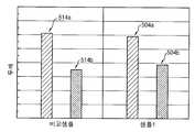
도 26에 도시된 것과 같이, 샘플 1의 알루미늄 산화막(502)은 비교 샘플 1의 알루미늄 산화막(512)과 비교할 때 낮은 식각율을 가짐을 알 수 있었다. 이와같이, 샘플 1의 알루미늄 산화막(502)은 상기 비교 샘플 1의 알루미늄 산화막(512)에 비해 치밀도가 높음을 알 수 있었다. 또한, 상기 샘플 1의 알루미늄 산화막(502)은 식각율이 상대적으로 낮으므로 용이하게 식각을 제어할 수 있음을 알 수 있었다.As shown in FIG. 26, it can be seen that the
막의 수축율 측정Membrane shrinkage measurement
상기 샘플 1 및 비교 샘플 1에 증착된 알루미늄 산화막에 대해, 결정화를 위한 어닐을 수행하였다. 다음에, 상기 어닐 공정 전 후의 알루미늄 산화막의 두께를 각각 측정하였다. 상기 어닐 공정은 1000℃의 온도에서 진행하였다.Annealing for crystallization was performed on the aluminum oxide film deposited on the
도 27은 샘플 1 및 비교 샘플 1에 대하여 결정화를 위한 어닐 전 후의 알루 미늄 산화막의 두께를 측정한 결과이다.27 is a result of measuring the thickness of the aluminum oxide film before and after annealing for crystallization for
도 287 도시된 것과 같이, 샘플 1의 알루미늄 산화막은 상기 결정화를 위한 어닐을 수행한 후에 두께가 약 10% 정도 감소되었다. 반면에, 비교 샘플 1의 알루미늄 산화막은 상기 결정화를 위한 어닐을 수행한 후에 두께가 약 13% 정도 감소되었다. 이와같이, 샘플 1의 알루미늄 산화막은 상기 비교 샘플 1의 알루미늄 산화막보다 결정화를 위한 어닐에 의해 막의 수축이 더 작게 발생됨을 알 수 있었다. 그러므로, 상기 샘플 1의 알루미늄 산화막의 치밀도가 상대적으로 더 높음을 알 수 있었다.As shown in FIG. 287, the aluminum oxide film of
막의 누설 전류 특성 측정Measurement of leakage current characteristics of membrane
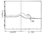
상기 샘플 1 및 비교 샘플 1에 형성된 알루미늄 산화막의 양단에 각각 전기장을 형성시키고, 상기 알루미늄 산화막을 통해 흐르는 전류 밀도를 각각 측정하였다.Electric fields were formed at both ends of the aluminum oxide film formed in the
도 28은 샘플 1 및 비교 샘플 1의 알루미늄 산화막에 대하여 전기장에 따른 전류밀도를 측정한 결과이다.FIG. 28 is a result of measuring current density according to an electric field with respect to aluminum oxide films of
도 28에 도시된 것과 같이, 동일한 전기장에서 샘플 1의 알루미늄 산화막은 상기 비교 샘플 1의 알루미늄 산화막에 비해 더 작은 전류 밀도가 측정되었다. 그 결과, 상기 샘플 1의 알루미늄 산화막은 상기 비교 샘플 1의 알루미늄 산화막에 비해 누설 전류가 더 작게 발생됨을 알 수 있었다.As shown in FIG. 28, in the same electric field, the aluminum oxide film of
막 내의 수소 함량 측정Determination of hydrogen content in the membrane
상기 샘플 1 및 비교 샘플 1에 형성된 알루미늄 산화막에 포함되어 있는 수 소 함량을 측정하였다. 상기 수소 함량은 SIMS(Secondary Ion Mass Spectroscopy)를 이용하여 측정하였다.The hydrogen content contained in the aluminum oxide film formed on the
도 29는 샘플 1 및 비교 샘플 1의 알루미늄 산화막에 대하여 수소 함량을 측정한 결과이다.29 is a result of measuring the hydrogen content of the aluminum oxide film of
도 29에 도시된 것과 같이, 상기 샘플 1의 알루미늄 산화막은 상기 비교 샘플 1의 알루미늄 산화막에 비해 수소 함량이 더 작았다. 이와같이, 상기 샘플 1의 알루미늄 산화막은 상기 비교 샘플 1의 알루미늄 산화막에 비해 불순물이 더 작게 발생되었으며, 그 결과 막 내의 트랩이 더 감소됨을 알 수 있었다.As shown in FIG. 29, the aluminum oxide film of
도 30은 본 발명의 일 실시예에 따라 제조되는 반도체 소자를 포함하는 장치를 도시한다.30 illustrates an apparatus including a semiconductor device fabricated in accordance with one embodiment of the present invention.
도시된 바와 같이, 본 실시예에 따른 장치는 메모리(610) 및 메모리 컨트롤러(620)가 메모리 카드(630)로 구현된다.As shown, in the apparatus according to the present embodiment, the
상기 메모리(610)는 상술한 본 발명의 실시예들에 따른 방법으로 제조되는 플래시 메모리 소자 또는 디램 소자를 포함할 수 있다. 메모리 컨트롤러(620)는 메모리(610)의 동작을 제어하는 입력 신호를 공급할 수 있다. 예를들어 메모리 제어기(610)는 명령어 및 어드레스 신호를 제공할 수 있다. 메모리 컨트롤러(620)는 수신한 제어신호에 기초해서 메모리(610)를 제어할 수 있다.The
상기 메모리 카드(630)는 디지털 카메라, 퍼스널 컴퓨터 등의 소비자 전자 장치와 함께 사용되기 위한 표준을 만족하는 메모리 카드일 수 있다. 메모리 컨트 롤러(620)는 메모리 카드(630)가 다른 장치, 예를들어 외부 장치로부터 수신한 제어신호에 기초해서 메모리(610)를 제어할 수 있다.The
도 31은 일 실시예에 따라 제조되는 반도체 소자를 포함하는 휴대장치를 도시한다.31 illustrates a portable device including a semiconductor device manufactured according to an embodiment.
도시된 바와 같이, 휴대장치(700)는 MP3, 비디오 재생기, 비디오 및 오디오 재생기 등일 수 있다. 도시된 바와 같이, 휴대장치(700)는 메모리(610) 및 메모리 컨트롤러(620)를 포함한다. 메모리(610)는 상술한 실시예들에 따라 제조되는 반도체 메모리 소자를 포함한다. 휴대장치(700)는 인코더 및 디코더(EDC)(710), 표시부재(720) 및 인터페이스(730)를 포함할 수 있다. 데이터(비디오, 오디오 등)는 메모리 컨트롤러(620)를 경유하여 메모리(610)와 인코더 및 디코더(EDC)(710) 사이에서 서로 주고받을 수 있다. 점선으로 표시된 바와 같이, 데이터는 메모리(610)와 인코더 및 디코더(EDC)(710) 사이에서 직접적으로 주고받을 수 있다.As shown, the
EDC(710)는 메모리(610)에 저장될 데이터를 인코드할 수 있다. 예를들어, EDC(710)는 오디오 데이터를 MP3 인코딩하여 메모리(610)에 저장할 수 있다. 또는, EDC(710)는 MPEG 비디오 데이터를 인코딩(예를들어, MPEG3, MPEG3, MPEG4 등)하여 메모리(610)에 저장할 수 있다. 또, EDC(710)는 다른 데이터 포맷에 따른 다른 유형의 데이터를 인코딩하는 다수의 인코더를 포함할 수 있다. 예를들어, EDC(710)는 오디오 데이터를 위한 MP3 인코더 및 비디오 데이터를 위한 MPEG 인코더를 포함할 수 있다. EDC(710)는 메모리(610)에서 출력되는 데이터를 디코드할 수 있다. 예를 들어 EDC(710)는 메모리(610)에서 출력되는 오디오 데이터를 MP3 디코딩할 수 있 다. 또는, EDC(710)는 메모리(610)에서 출력되는 비디오 데이터를 MPEG 디코딩(예를 들어, MPEG3, MPEG3, MPEG4 등)할 수 있다. 또, EDC(710)는 다른 데이터 포맷에 따른 다른 유형의 데이터를 디코딩 다수의 디코더를 포함할 수 있다.The
예를 들어 EDC(710)는 오디오 데이터를 위한 MP3 디코더 및 비디오 데이터를 위한 MPEG 디코더를 포함할 수 있다. 또 EDC(710)는 디코더만을 포함할 수도 있다. 예를 들어 이미 인코드된 데이터가 EDC(710)에 전달되어 디코딩된 후 메모리 컨트롤러(620) 그리고/또는 메모리(610)에 전달될 수 있다.For example, the
EDC(710)는 인터페이스(730)를 경유하여 인코딩을 위한 데이터 또는 이미 인코드된 데이터를 수신한다. 인터페이스(730)는 잘 알려진 표준(예를 들어 USB, 파이어와이어 등)을 따를 수 있다. 인터페이스(730)는 또한 하나 이상의 인터페이스를 포함할 수 있다. 예를 들어 인터페이스(730)는 파이어와이어(firewire) 인터페이스, USB 인터페이스 등을 포함할 수 있다. 메모리(610)로부터 제공된 데이터는 또한 인터페이스(730)를 거쳐 출력될 수 있다.
표시부재(720)는 메모리(610) 그리고/또는 EDC(710)에 의해 디코딩된 데이터를 사용자가 인식할 수 있도록 표시한다. 예를 들어, 표시부재(720)는 비디오 데이터 등을 출력하는 표시 스크린, 오디오 데이터를 출력하는 스피커 잭 등을 포함할 수 있다. The
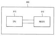
도 32는 일 실시예에 따라 제조되는 반도체 소자를 포함하는 장치를 도시한다. 도시된 바와 같이 본 실시예의 장치에 따르면, 메모리(610)는 컴퓨터 시스템(800) 내의 중앙처리장치(CPU)(810)에 연결될 수 있다.32 illustrates an apparatus including a semiconductor device manufactured according to one embodiment. As shown, in accordance with the device of this embodiment,
예를 들어 컴퓨터 시스템(800)은 퍼스널 컴퓨터, 퍼스널 데이터 어시스턴트(assistant) 등일 수 있다. 메모리(610)는 중앙처리장치(810)에 버스(bus)를 통해서 연결될 수 있다.For example,
도 33은 일 실시예에 따라 제조되는 반도체 소자를 포함하는 장치를 도시한다. 도시된 바와 같이 본 실시예에 따른 장치(900)는 컨트롤러(910), 키보드, 디스플레이 등의 입출력 장치(920), 메모리(610), 인터페이스(930)를 포함할 수 있다. 본 실시예에서 장치의 각 구성은 버스(950)를 통해서 서로 연결될 수 있다. 컨트롤러(910)는 하나 이상의 마이크로프로세서, 디지털 프로세서, 마이크로컨트롤러, 또는 프로세서를 포함할 수 있다. 메모리(610)는 데이터 그리고/또는 컨트롤러(910)에 의해 실행된 명령을 저장할 수 있다. 인터페이스(930)는 다른 시스템 예를 들어 통신 네트워크로부터 또는 통신 네트워크로 데이터를 전송하는 데 사용될 수 있다. 장치(900)는 PDA 같은 모바일 시스템, 휴대용 컴퓨터, 웹 타블렛(Web tablet), 무선 전화기, 모바일 전화기, 디지털 음악 재생기, 메모리 카드 또는 정보를 송신 그리고/또는 수신할 수 있는 다른 시스템일 수 있다.33 illustrates an apparatus including a semiconductor device manufactured according to one embodiment. As shown, the
상기 설명한 것과 같이, 본 발명에 의하면 불순물이 감소되고 높은 밀도를 갖는 우수한 특성의 알루미늄 산화물을 형성할 수 있다. 본 발명에 따른 알루미늄 산화물은 반도체 소자에 포함되는 유전막을 형성할 때 사용될 수 있다.As described above, according to the present invention, it is possible to form aluminum oxide of excellent properties with reduced impurities and high density. The aluminum oxide according to the present invention can be used when forming a dielectric film included in a semiconductor device.
도 1은 본 발명에 따른 유전막을 형성하기에 적합한 증착 반응기를 나타낸다.1 shows a deposition reactor suitable for forming a dielectric film according to the present invention.
도 2는 발명의 실시예 1에 따른 알루미늄 산화막을 형성하는 방법을 나타낸다.2 shows a method of forming an aluminum oxide film according to Example 1 of the invention.
도 3은 도 1에 도시한 알루미늄 산화막을 포함하는 플래시 메모리 소자의 평면도이다.3 is a plan view of a flash memory device including the aluminum oxide film shown in FIG. 1.
도 4는 도 3에 도시한 플래시 메모리 소자의 단면도이다.4 is a cross-sectional view of the flash memory device shown in FIG. 3.
도 5 내지 도 8은 도 3 및 도 4에 도시된 플래시 메모리 소자의 제조 방법을 설명하기 위한 단면도들이다.5 to 8 are cross-sectional views illustrating a method of manufacturing the flash memory device illustrated in FIGS. 3 and 4.
도 9는 본 발명의 실시예 2에 따른 플래시 메모리 소자를 나타낸다.9 shows a flash memory device according to
도 10a는 본 발명의 실시예 3에 따른 수직형 NAND 플래시 메모리 소자를 나타내는 사시도이다.10A is a perspective view illustrating a vertical NAND flash memory device according to
도 10b는 도 10a에 도시된 수직형 NAND 플래시 메모리 소자를 나타내는 단면도이다.FIG. 10B is a cross-sectional view illustrating the vertical NAND flash memory device illustrated in FIG. 10A.
도 11 내지 도 19는 도 10a 및 도 10b에 도시된 수직형 NAND 플래시 메모리 소자의 제조 방법을 나타내는 단면도이다.11 to 19 are cross-sectional views illustrating a method of manufacturing the vertical NAND flash memory device illustrated in FIGS. 10A and 10B.
도 20은 본 발명의 실시예 4에 따른 커패시터를 나타낸다.20 shows a capacitor according to
도 21은 본 발명의 실시예 5에 따른 디램 소자를 나타낸다.21 illustrates a DRAM device according to Embodiment 5 of the present invention.
도 22 내지 도 24는 디램 소자의 제조 방법을 나타내는 단면도들이다.22 to 24 are cross-sectional views illustrating a method of manufacturing a DRAM device.
도 25는 상기 샘플 1 및 비교 샘플 1에 대하여 막의 밀도를 측정한 결과이다.FIG. 25 is a result of measuring the density of the membrane for
도 26은 상기 샘플 1 및 비교 샘플 1에 대하여 식각 공정 시간이 경과함에 따른 알루미늄 산화막의 식각된 두께를 측정한 결과이다.FIG. 26 illustrates a result of measuring the etched thickness of the aluminum oxide layer as the etching process time passes with respect to the
도 27은 샘플 1 및 비교 샘플 1에 대하여 결정화를 위한 어닐 전 후의 알루미늄 산화막의 두께를 측정한 결과이다.27 is a result of measuring the thickness of the aluminum oxide film before and after annealing for crystallization for
도 28은 샘플 1 및 비교 샘플 1의 알루미늄 산화막에 대하여 전기장에 따른 전류밀도를 측정한 결과이다.FIG. 28 is a result of measuring current density according to an electric field with respect to aluminum oxide films of
도 29는 샘플 1 및 비교 샘플 1의 알루미늄 산화막에 대하여 수소 함량을 측정한 결과이다.29 is a result of measuring the hydrogen content of the aluminum oxide film of
도 30은 본 발명의 일 실시예에 따라 제조되는 반도체 소자를 포함하는 장치를 도시한다.30 illustrates an apparatus including a semiconductor device fabricated in accordance with one embodiment of the present invention.
도 31은 일 실시예에 따라 제조되는 반도체 소자를 포함하는 휴대장치를 도시한다.31 illustrates a portable device including a semiconductor device manufactured according to an embodiment.
도 32는 일 실시예에 따라 제조되는 반도체 소자를 포함하는 장치를 도시한다.32 illustrates an apparatus including a semiconductor device manufactured according to one embodiment.
도 33은 일 실시예에 따라 제조되는 반도체 소자를 포함하는 장치를 도시한다.33 illustrates an apparatus including a semiconductor device manufactured according to one embodiment.
Claims (10)
Translated fromKoreanPriority Applications (2)
| Application Number | Priority Date | Filing Date | Title |
|---|---|---|---|
| KR1020090135106AKR20110078326A (en) | 2009-12-31 | 2009-12-31 | Dielectric film forming method and semiconductor device manufacturing method using same |
| US12/975,071US20110159680A1 (en) | 2009-12-31 | 2010-12-21 | Method of forming a dielectric layer and method of manufacturing a semiconductor device using the same |
Applications Claiming Priority (1)
| Application Number | Priority Date | Filing Date | Title |
|---|---|---|---|
| KR1020090135106AKR20110078326A (en) | 2009-12-31 | 2009-12-31 | Dielectric film forming method and semiconductor device manufacturing method using same |
Publications (1)
| Publication Number | Publication Date |
|---|---|
| KR20110078326Atrue KR20110078326A (en) | 2011-07-07 |
Family
ID=44188062
Family Applications (1)
| Application Number | Title | Priority Date | Filing Date |
|---|---|---|---|
| KR1020090135106AWithdrawnKR20110078326A (en) | 2009-12-31 | 2009-12-31 | Dielectric film forming method and semiconductor device manufacturing method using same |
Country Status (2)
| Country | Link |
|---|---|
| US (1) | US20110159680A1 (en) |
| KR (1) | KR20110078326A (en) |
Cited By (1)
| Publication number | Priority date | Publication date | Assignee | Title |
|---|---|---|---|---|
| KR101432910B1 (en)* | 2012-03-16 | 2014-08-21 | 후지쯔 가부시끼가이샤 | Method of fabricating semiconductor device and semiconductor device |
Families Citing this family (362)
| Publication number | Priority date | Publication date | Assignee | Title |
|---|---|---|---|---|
| US10378106B2 (en) | 2008-11-14 | 2019-08-13 | Asm Ip Holding B.V. | Method of forming insulation film by modified PEALD |
| US9394608B2 (en) | 2009-04-06 | 2016-07-19 | Asm America, Inc. | Semiconductor processing reactor and components thereof |
| US8802201B2 (en) | 2009-08-14 | 2014-08-12 | Asm America, Inc. | Systems and methods for thin-film deposition of metal oxides using excited nitrogen-oxygen species |
| US9312155B2 (en) | 2011-06-06 | 2016-04-12 | Asm Japan K.K. | High-throughput semiconductor-processing apparatus equipped with multiple dual-chamber modules |
| US10364496B2 (en) | 2011-06-27 | 2019-07-30 | Asm Ip Holding B.V. | Dual section module having shared and unshared mass flow controllers |
| US10854498B2 (en) | 2011-07-15 | 2020-12-01 | Asm Ip Holding B.V. | Wafer-supporting device and method for producing same |
| US20130023129A1 (en) | 2011-07-20 | 2013-01-24 | Asm America, Inc. | Pressure transmitter for a semiconductor processing environment |
| US9017481B1 (en) | 2011-10-28 | 2015-04-28 | Asm America, Inc. | Process feed management for semiconductor substrate processing |
| US9659799B2 (en) | 2012-08-28 | 2017-05-23 | Asm Ip Holding B.V. | Systems and methods for dynamic semiconductor process scheduling |
| US9021985B2 (en) | 2012-09-12 | 2015-05-05 | Asm Ip Holdings B.V. | Process gas management for an inductively-coupled plasma deposition reactor |
| US10714315B2 (en) | 2012-10-12 | 2020-07-14 | Asm Ip Holdings B.V. | Semiconductor reaction chamber showerhead |
| US20160376700A1 (en) | 2013-02-01 | 2016-12-29 | Asm Ip Holding B.V. | System for treatment of deposition reactor |
| US9589770B2 (en) | 2013-03-08 | 2017-03-07 | Asm Ip Holding B.V. | Method and systems for in-situ formation of intermediate reactive species |
| US9484191B2 (en) | 2013-03-08 | 2016-11-01 | Asm Ip Holding B.V. | Pulsed remote plasma method and system |
| EP3011596B1 (en)* | 2013-07-11 | 2019-01-09 | Yissum Research Development Company of the Hebrew University of Jerusalem Ltd. | Thermal doping by vacancy formation in nanocrystals |
| US9240412B2 (en) | 2013-09-27 | 2016-01-19 | Asm Ip Holding B.V. | Semiconductor structure and device and methods of forming same using selective epitaxial process |
| US10683571B2 (en) | 2014-02-25 | 2020-06-16 | Asm Ip Holding B.V. | Gas supply manifold and method of supplying gases to chamber using same |
| US10167557B2 (en) | 2014-03-18 | 2019-01-01 | Asm Ip Holding B.V. | Gas distribution system, reactor including the system, and methods of using the same |
| US11015245B2 (en) | 2014-03-19 | 2021-05-25 | Asm Ip Holding B.V. | Gas-phase reactor and system having exhaust plenum and components thereof |
| US10858737B2 (en) | 2014-07-28 | 2020-12-08 | Asm Ip Holding B.V. | Showerhead assembly and components thereof |
| US9890456B2 (en) | 2014-08-21 | 2018-02-13 | Asm Ip Holding B.V. | Method and system for in situ formation of gas-phase compounds |
| US9657845B2 (en) | 2014-10-07 | 2017-05-23 | Asm Ip Holding B.V. | Variable conductance gas distribution apparatus and method |
| US10941490B2 (en) | 2014-10-07 | 2021-03-09 | Asm Ip Holding B.V. | Multiple temperature range susceptor, assembly, reactor and system including the susceptor, and methods of using the same |
| KR102300403B1 (en) | 2014-11-19 | 2021-09-09 | 에이에스엠 아이피 홀딩 비.브이. | Method of depositing thin film |
| KR102263121B1 (en)* | 2014-12-22 | 2021-06-09 | 에이에스엠 아이피 홀딩 비.브이. | Semiconductor device and manufacuring method thereof |
| US10529542B2 (en) | 2015-03-11 | 2020-01-07 | Asm Ip Holdings B.V. | Cross-flow reactor and method |
| US10276355B2 (en) | 2015-03-12 | 2019-04-30 | Asm Ip Holding B.V. | Multi-zone reactor, system including the reactor, and method of using the same |
| US10458018B2 (en) | 2015-06-26 | 2019-10-29 | Asm Ip Holding B.V. | Structures including metal carbide material, devices including the structures, and methods of forming same |
| US10600673B2 (en) | 2015-07-07 | 2020-03-24 | Asm Ip Holding B.V. | Magnetic susceptor to baseplate seal |
| US10043661B2 (en) | 2015-07-13 | 2018-08-07 | Asm Ip Holding B.V. | Method for protecting layer by forming hydrocarbon-based extremely thin film |
| US10083836B2 (en) | 2015-07-24 | 2018-09-25 | Asm Ip Holding B.V. | Formation of boron-doped titanium metal films with high work function |
| US9960072B2 (en) | 2015-09-29 | 2018-05-01 | Asm Ip Holding B.V. | Variable adjustment for precise matching of multiple chamber cavity housings |
| US10211308B2 (en) | 2015-10-21 | 2019-02-19 | Asm Ip Holding B.V. | NbMC layers |
| US10322384B2 (en) | 2015-11-09 | 2019-06-18 | Asm Ip Holding B.V. | Counter flow mixer for process chamber |
| US11139308B2 (en) | 2015-12-29 | 2021-10-05 | Asm Ip Holding B.V. | Atomic layer deposition of III-V compounds to form V-NAND devices |
| US10529554B2 (en) | 2016-02-19 | 2020-01-07 | Asm Ip Holding B.V. | Method for forming silicon nitride film selectively on sidewalls or flat surfaces of trenches |
| US10468251B2 (en) | 2016-02-19 | 2019-11-05 | Asm Ip Holding B.V. | Method for forming spacers using silicon nitride film for spacer-defined multiple patterning |
| US10501866B2 (en) | 2016-03-09 | 2019-12-10 | Asm Ip Holding B.V. | Gas distribution apparatus for improved film uniformity in an epitaxial system |
| US10343920B2 (en) | 2016-03-18 | 2019-07-09 | Asm Ip Holding B.V. | Aligned carbon nanotubes |
| US9892913B2 (en) | 2016-03-24 | 2018-02-13 | Asm Ip Holding B.V. | Radial and thickness control via biased multi-port injection settings |
| US10087522B2 (en) | 2016-04-21 | 2018-10-02 | Asm Ip Holding B.V. | Deposition of metal borides |
| US10190213B2 (en) | 2016-04-21 | 2019-01-29 | Asm Ip Holding B.V. | Deposition of metal borides |
| US10865475B2 (en) | 2016-04-21 | 2020-12-15 | Asm Ip Holding B.V. | Deposition of metal borides and silicides |
| US10032628B2 (en) | 2016-05-02 | 2018-07-24 | Asm Ip Holding B.V. | Source/drain performance through conformal solid state doping |
| US10367080B2 (en) | 2016-05-02 | 2019-07-30 | Asm Ip Holding B.V. | Method of forming a germanium oxynitride film |
| KR102592471B1 (en) | 2016-05-17 | 2023-10-20 | 에이에스엠 아이피 홀딩 비.브이. | Method of forming metal interconnection and method of fabricating semiconductor device using the same |
| US11453943B2 (en) | 2016-05-25 | 2022-09-27 | Asm Ip Holding B.V. | Method for forming carbon-containing silicon/metal oxide or nitride film by ALD using silicon precursor and hydrocarbon precursor |
| US10388509B2 (en) | 2016-06-28 | 2019-08-20 | Asm Ip Holding B.V. | Formation of epitaxial layers via dislocation filtering |
| US9859151B1 (en) | 2016-07-08 | 2018-01-02 | Asm Ip Holding B.V. | Selective film deposition method to form air gaps |
| US10612137B2 (en) | 2016-07-08 | 2020-04-07 | Asm Ip Holdings B.V. | Organic reactants for atomic layer deposition |
| US9793135B1 (en) | 2016-07-14 | 2017-10-17 | ASM IP Holding B.V | Method of cyclic dry etching using etchant film |
| US10714385B2 (en) | 2016-07-19 | 2020-07-14 | Asm Ip Holding B.V. | Selective deposition of tungsten |
| KR102354490B1 (en) | 2016-07-27 | 2022-01-21 | 에이에스엠 아이피 홀딩 비.브이. | Method of processing a substrate |
| US9887082B1 (en) | 2016-07-28 | 2018-02-06 | Asm Ip Holding B.V. | Method and apparatus for filling a gap |
| KR102532607B1 (en) | 2016-07-28 | 2023-05-15 | 에이에스엠 아이피 홀딩 비.브이. | Substrate processing apparatus and method of operating the same |
| US10395919B2 (en) | 2016-07-28 | 2019-08-27 | Asm Ip Holding B.V. | Method and apparatus for filling a gap |
| US10177025B2 (en) | 2016-07-28 | 2019-01-08 | Asm Ip Holding B.V. | Method and apparatus for filling a gap |
| US9812320B1 (en) | 2016-07-28 | 2017-11-07 | Asm Ip Holding B.V. | Method and apparatus for filling a gap |
| US10090316B2 (en) | 2016-09-01 | 2018-10-02 | Asm Ip Holding B.V. | 3D stacked multilayer semiconductor memory using doped select transistor channel |
| US10410943B2 (en) | 2016-10-13 | 2019-09-10 | Asm Ip Holding B.V. | Method for passivating a surface of a semiconductor and related systems |
| US10643826B2 (en) | 2016-10-26 | 2020-05-05 | Asm Ip Holdings B.V. | Methods for thermally calibrating reaction chambers |
| US11532757B2 (en) | 2016-10-27 | 2022-12-20 | Asm Ip Holding B.V. | Deposition of charge trapping layers |
| US10643904B2 (en) | 2016-11-01 | 2020-05-05 | Asm Ip Holdings B.V. | Methods for forming a semiconductor device and related semiconductor device structures |
| US10435790B2 (en) | 2016-11-01 | 2019-10-08 | Asm Ip Holding B.V. | Method of subatmospheric plasma-enhanced ALD using capacitively coupled electrodes with narrow gap |
| US10714350B2 (en) | 2016-11-01 | 2020-07-14 | ASM IP Holdings, B.V. | Methods for forming a transition metal niobium nitride film on a substrate by atomic layer deposition and related semiconductor device structures |
| US10229833B2 (en) | 2016-11-01 | 2019-03-12 | Asm Ip Holding B.V. | Methods for forming a transition metal nitride film on a substrate by atomic layer deposition and related semiconductor device structures |
| US10134757B2 (en) | 2016-11-07 | 2018-11-20 | Asm Ip Holding B.V. | Method of processing a substrate and a device manufactured by using the method |
| KR102546317B1 (en) | 2016-11-15 | 2023-06-21 | 에이에스엠 아이피 홀딩 비.브이. | Gas supply unit and substrate processing apparatus including the same |
| US10340135B2 (en) | 2016-11-28 | 2019-07-02 | Asm Ip Holding B.V. | Method of topologically restricted plasma-enhanced cyclic deposition of silicon or metal nitride |
| KR102762543B1 (en) | 2016-12-14 | 2025-02-05 | 에이에스엠 아이피 홀딩 비.브이. | Substrate processing apparatus |
| US11581186B2 (en) | 2016-12-15 | 2023-02-14 | Asm Ip Holding B.V. | Sequential infiltration synthesis apparatus |
| US11447861B2 (en) | 2016-12-15 | 2022-09-20 | Asm Ip Holding B.V. | Sequential infiltration synthesis apparatus and a method of forming a patterned structure |
| US9916980B1 (en) | 2016-12-15 | 2018-03-13 | Asm Ip Holding B.V. | Method of forming a structure on a substrate |
| KR102700194B1 (en) | 2016-12-19 | 2024-08-28 | 에이에스엠 아이피 홀딩 비.브이. | Substrate processing apparatus |
| US10269558B2 (en) | 2016-12-22 | 2019-04-23 | Asm Ip Holding B.V. | Method of forming a structure on a substrate |
| US10867788B2 (en) | 2016-12-28 | 2020-12-15 | Asm Ip Holding B.V. | Method of forming a structure on a substrate |
| US11390950B2 (en) | 2017-01-10 | 2022-07-19 | Asm Ip Holding B.V. | Reactor system and method to reduce residue buildup during a film deposition process |
| US10655221B2 (en) | 2017-02-09 | 2020-05-19 | Asm Ip Holding B.V. | Method for depositing oxide film by thermal ALD and PEALD |
| US10468261B2 (en) | 2017-02-15 | 2019-11-05 | Asm Ip Holding B.V. | Methods for forming a metallic film on a substrate by cyclical deposition and related semiconductor device structures |
| US10283353B2 (en) | 2017-03-29 | 2019-05-07 | Asm Ip Holding B.V. | Method of reforming insulating film deposited on substrate with recess pattern |
| US10529563B2 (en) | 2017-03-29 | 2020-01-07 | Asm Ip Holdings B.V. | Method for forming doped metal oxide films on a substrate by cyclical deposition and related semiconductor device structures |
| US10103040B1 (en) | 2017-03-31 | 2018-10-16 | Asm Ip Holding B.V. | Apparatus and method for manufacturing a semiconductor device |
| USD830981S1 (en) | 2017-04-07 | 2018-10-16 | Asm Ip Holding B.V. | Susceptor for semiconductor substrate processing apparatus |
| KR102457289B1 (en) | 2017-04-25 | 2022-10-21 | 에이에스엠 아이피 홀딩 비.브이. | Method for depositing a thin film and manufacturing a semiconductor device |
| US10446393B2 (en) | 2017-05-08 | 2019-10-15 | Asm Ip Holding B.V. | Methods for forming silicon-containing epitaxial layers and related semiconductor device structures |
| US10892156B2 (en) | 2017-05-08 | 2021-01-12 | Asm Ip Holding B.V. | Methods for forming a silicon nitride film on a substrate and related semiconductor device structures |
| US10770286B2 (en) | 2017-05-08 | 2020-09-08 | Asm Ip Holdings B.V. | Methods for selectively forming a silicon nitride film on a substrate and related semiconductor device structures |
| US10504742B2 (en) | 2017-05-31 | 2019-12-10 | Asm Ip Holding B.V. | Method of atomic layer etching using hydrogen plasma |
| US10886123B2 (en) | 2017-06-02 | 2021-01-05 | Asm Ip Holding B.V. | Methods for forming low temperature semiconductor layers and related semiconductor device structures |
| US12040200B2 (en) | 2017-06-20 | 2024-07-16 | Asm Ip Holding B.V. | Semiconductor processing apparatus and methods for calibrating a semiconductor processing apparatus |
| US11306395B2 (en) | 2017-06-28 | 2022-04-19 | Asm Ip Holding B.V. | Methods for depositing a transition metal nitride film on a substrate by atomic layer deposition and related deposition apparatus |
| US10685834B2 (en) | 2017-07-05 | 2020-06-16 | Asm Ip Holdings B.V. | Methods for forming a silicon germanium tin layer and related semiconductor device structures |
| KR20190009245A (en) | 2017-07-18 | 2019-01-28 | 에이에스엠 아이피 홀딩 비.브이. | Methods for forming a semiconductor device structure and related semiconductor device structures |
| US11374112B2 (en) | 2017-07-19 | 2022-06-28 | Asm Ip Holding B.V. | Method for depositing a group IV semiconductor and related semiconductor device structures |
| US11018002B2 (en) | 2017-07-19 | 2021-05-25 | Asm Ip Holding B.V. | Method for selectively depositing a Group IV semiconductor and related semiconductor device structures |
| US10541333B2 (en) | 2017-07-19 | 2020-01-21 | Asm Ip Holding B.V. | Method for depositing a group IV semiconductor and related semiconductor device structures |
| US10605530B2 (en) | 2017-07-26 | 2020-03-31 | Asm Ip Holding B.V. | Assembly of a liner and a flange for a vertical furnace as well as the liner and the vertical furnace |
| US10590535B2 (en) | 2017-07-26 | 2020-03-17 | Asm Ip Holdings B.V. | Chemical treatment, deposition and/or infiltration apparatus and method for using the same |
| US10312055B2 (en) | 2017-07-26 | 2019-06-04 | Asm Ip Holding B.V. | Method of depositing film by PEALD using negative bias |
| TWI815813B (en) | 2017-08-04 | 2023-09-21 | 荷蘭商Asm智慧財產控股公司 | Showerhead assembly for distributing a gas within a reaction chamber |
| US10692741B2 (en) | 2017-08-08 | 2020-06-23 | Asm Ip Holdings B.V. | Radiation shield |
| US10770336B2 (en) | 2017-08-08 | 2020-09-08 | Asm Ip Holding B.V. | Substrate lift mechanism and reactor including same |
| US11769682B2 (en) | 2017-08-09 | 2023-09-26 | Asm Ip Holding B.V. | Storage apparatus for storing cassettes for substrates and processing apparatus equipped therewith |
| US10249524B2 (en) | 2017-08-09 | 2019-04-02 | Asm Ip Holding B.V. | Cassette holder assembly for a substrate cassette and holding member for use in such assembly |
| US11139191B2 (en) | 2017-08-09 | 2021-10-05 | Asm Ip Holding B.V. | Storage apparatus for storing cassettes for substrates and processing apparatus equipped therewith |
| US10236177B1 (en) | 2017-08-22 | 2019-03-19 | ASM IP Holding B.V.. | Methods for depositing a doped germanium tin semiconductor and related semiconductor device structures |
| USD900036S1 (en) | 2017-08-24 | 2020-10-27 | Asm Ip Holding B.V. | Heater electrical connector and adapter |
| US11830730B2 (en) | 2017-08-29 | 2023-11-28 | Asm Ip Holding B.V. | Layer forming method and apparatus |
| KR102491945B1 (en) | 2017-08-30 | 2023-01-26 | 에이에스엠 아이피 홀딩 비.브이. | Substrate processing apparatus |
| US11056344B2 (en) | 2017-08-30 | 2021-07-06 | Asm Ip Holding B.V. | Layer forming method |
| US11295980B2 (en) | 2017-08-30 | 2022-04-05 | Asm Ip Holding B.V. | Methods for depositing a molybdenum metal film over a dielectric surface of a substrate by a cyclical deposition process and related semiconductor device structures |
| KR102401446B1 (en) | 2017-08-31 | 2022-05-24 | 에이에스엠 아이피 홀딩 비.브이. | Substrate processing apparatus |
| US10607895B2 (en) | 2017-09-18 | 2020-03-31 | Asm Ip Holdings B.V. | Method for forming a semiconductor device structure comprising a gate fill metal |
| KR102630301B1 (en) | 2017-09-21 | 2024-01-29 | 에이에스엠 아이피 홀딩 비.브이. | Method of sequential infiltration synthesis treatment of infiltrateable material and structures and devices formed using same |
| US10844484B2 (en) | 2017-09-22 | 2020-11-24 | Asm Ip Holding B.V. | Apparatus for dispensing a vapor phase reactant to a reaction chamber and related methods |
| US10658205B2 (en) | 2017-09-28 | 2020-05-19 | Asm Ip Holdings B.V. | Chemical dispensing apparatus and methods for dispensing a chemical to a reaction chamber |
| US10403504B2 (en) | 2017-10-05 | 2019-09-03 | Asm Ip Holding B.V. | Method for selectively depositing a metallic film on a substrate |
| US10319588B2 (en) | 2017-10-10 | 2019-06-11 | Asm Ip Holding B.V. | Method for depositing a metal chalcogenide on a substrate by cyclical deposition |
| US10923344B2 (en) | 2017-10-30 | 2021-02-16 | Asm Ip Holding B.V. | Methods for forming a semiconductor structure and related semiconductor structures |
| KR102443047B1 (en) | 2017-11-16 | 2022-09-14 | 에이에스엠 아이피 홀딩 비.브이. | Method of processing a substrate and a device manufactured by the same |
| US10910262B2 (en) | 2017-11-16 | 2021-02-02 | Asm Ip Holding B.V. | Method of selectively depositing a capping layer structure on a semiconductor device structure |
| US11022879B2 (en) | 2017-11-24 | 2021-06-01 | Asm Ip Holding B.V. | Method of forming an enhanced unexposed photoresist layer |
| WO2019103613A1 (en) | 2017-11-27 | 2019-05-31 | Asm Ip Holding B.V. | A storage device for storing wafer cassettes for use with a batch furnace |
| CN111344522B (en) | 2017-11-27 | 2022-04-12 | 阿斯莫Ip控股公司 | Including clean mini-environment device |
| US10290508B1 (en) | 2017-12-05 | 2019-05-14 | Asm Ip Holding B.V. | Method for forming vertical spacers for spacer-defined patterning |
| US10872771B2 (en) | 2018-01-16 | 2020-12-22 | Asm Ip Holding B. V. | Method for depositing a material film on a substrate within a reaction chamber by a cyclical deposition process and related device structures |
| KR102695659B1 (en) | 2018-01-19 | 2024-08-14 | 에이에스엠 아이피 홀딩 비.브이. | Method for depositing a gap filling layer by plasma assisted deposition |
| TWI799494B (en) | 2018-01-19 | 2023-04-21 | 荷蘭商Asm 智慧財產控股公司 | Deposition method |
| USD903477S1 (en) | 2018-01-24 | 2020-12-01 | Asm Ip Holdings B.V. | Metal clamp |
| US11018047B2 (en) | 2018-01-25 | 2021-05-25 | Asm Ip Holding B.V. | Hybrid lift pin |
| USD880437S1 (en) | 2018-02-01 | 2020-04-07 | Asm Ip Holding B.V. | Gas supply plate for semiconductor manufacturing apparatus |
| US10535516B2 (en) | 2018-02-01 | 2020-01-14 | Asm Ip Holdings B.V. | Method for depositing a semiconductor structure on a surface of a substrate and related semiconductor structures |
| US11081345B2 (en) | 2018-02-06 | 2021-08-03 | Asm Ip Holding B.V. | Method of post-deposition treatment for silicon oxide film |
| US10896820B2 (en) | 2018-02-14 | 2021-01-19 | Asm Ip Holding B.V. | Method for depositing a ruthenium-containing film on a substrate by a cyclical deposition process |
| WO2019158960A1 (en) | 2018-02-14 | 2019-08-22 | Asm Ip Holding B.V. | A method for depositing a ruthenium-containing film on a substrate by a cyclical deposition process |
| US10731249B2 (en) | 2018-02-15 | 2020-08-04 | Asm Ip Holding B.V. | Method of forming a transition metal containing film on a substrate by a cyclical deposition process, a method for supplying a transition metal halide compound to a reaction chamber, and related vapor deposition apparatus |
| KR102636427B1 (en) | 2018-02-20 | 2024-02-13 | 에이에스엠 아이피 홀딩 비.브이. | Substrate processing method and apparatus |
| US10658181B2 (en) | 2018-02-20 | 2020-05-19 | Asm Ip Holding B.V. | Method of spacer-defined direct patterning in semiconductor fabrication |
| US10975470B2 (en) | 2018-02-23 | 2021-04-13 | Asm Ip Holding B.V. | Apparatus for detecting or monitoring for a chemical precursor in a high temperature environment |
| US11473195B2 (en) | 2018-03-01 | 2022-10-18 | Asm Ip Holding B.V. | Semiconductor processing apparatus and a method for processing a substrate |
| US11629406B2 (en) | 2018-03-09 | 2023-04-18 | Asm Ip Holding B.V. | Semiconductor processing apparatus comprising one or more pyrometers for measuring a temperature of a substrate during transfer of the substrate |
| US11114283B2 (en) | 2018-03-16 | 2021-09-07 | Asm Ip Holding B.V. | Reactor, system including the reactor, and methods of manufacturing and using same |
| KR102646467B1 (en) | 2018-03-27 | 2024-03-11 | 에이에스엠 아이피 홀딩 비.브이. | Method of forming an electrode on a substrate and a semiconductor device structure including an electrode |
| US11230766B2 (en) | 2018-03-29 | 2022-01-25 | Asm Ip Holding B.V. | Substrate processing apparatus and method |
| US10510536B2 (en) | 2018-03-29 | 2019-12-17 | Asm Ip Holding B.V. | Method of depositing a co-doped polysilicon film on a surface of a substrate within a reaction chamber |
| US11088002B2 (en) | 2018-03-29 | 2021-08-10 | Asm Ip Holding B.V. | Substrate rack and a substrate processing system and method |
| KR102501472B1 (en) | 2018-03-30 | 2023-02-20 | 에이에스엠 아이피 홀딩 비.브이. | Substrate processing method |
| KR102600229B1 (en) | 2018-04-09 | 2023-11-10 | 에이에스엠 아이피 홀딩 비.브이. | Substrate supporting device, substrate processing apparatus including the same and substrate processing method |
| US12025484B2 (en) | 2018-05-08 | 2024-07-02 | Asm Ip Holding B.V. | Thin film forming method |
| TWI811348B (en) | 2018-05-08 | 2023-08-11 | 荷蘭商Asm 智慧財產控股公司 | Methods for depositing an oxide film on a substrate by a cyclical deposition process and related device structures |
| US12272527B2 (en) | 2018-05-09 | 2025-04-08 | Asm Ip Holding B.V. | Apparatus for use with hydrogen radicals and method of using same |
| KR20190129718A (en) | 2018-05-11 | 2019-11-20 | 에이에스엠 아이피 홀딩 비.브이. | Methods for forming a doped metal carbide film on a substrate and related semiconductor device structures |
| KR102596988B1 (en) | 2018-05-28 | 2023-10-31 | 에이에스엠 아이피 홀딩 비.브이. | Method of processing a substrate and a device manufactured by the same |
| US11718913B2 (en) | 2018-06-04 | 2023-08-08 | Asm Ip Holding B.V. | Gas distribution system and reactor system including same |
| TWI840362B (en) | 2018-06-04 | 2024-05-01 | 荷蘭商Asm Ip私人控股有限公司 | Wafer handling chamber with moisture reduction |
| US11286562B2 (en) | 2018-06-08 | 2022-03-29 | Asm Ip Holding B.V. | Gas-phase chemical reactor and method of using same |
| US10797133B2 (en) | 2018-06-21 | 2020-10-06 | Asm Ip Holding B.V. | Method for depositing a phosphorus doped silicon arsenide film and related semiconductor device structures |
| KR102568797B1 (en) | 2018-06-21 | 2023-08-21 | 에이에스엠 아이피 홀딩 비.브이. | Substrate processing system |
| TWI873894B (en) | 2018-06-27 | 2025-02-21 | 荷蘭商Asm Ip私人控股有限公司 | Cyclic deposition methods for forming metal-containing material and films and structures including the metal-containing material |
| KR102854019B1 (en) | 2018-06-27 | 2025-09-02 | 에이에스엠 아이피 홀딩 비.브이. | Periodic deposition method for forming a metal-containing material and films and structures comprising the metal-containing material |
| US10612136B2 (en) | 2018-06-29 | 2020-04-07 | ASM IP Holding, B.V. | Temperature-controlled flange and reactor system including same |
| KR102686758B1 (en) | 2018-06-29 | 2024-07-18 | 에이에스엠 아이피 홀딩 비.브이. | Method for depositing a thin film and manufacturing a semiconductor device |
| US10388513B1 (en) | 2018-07-03 | 2019-08-20 | Asm Ip Holding B.V. | Method for depositing silicon-free carbon-containing film as gap-fill layer by pulse plasma-assisted deposition |
| US10755922B2 (en) | 2018-07-03 | 2020-08-25 | Asm Ip Holding B.V. | Method for depositing silicon-free carbon-containing film as gap-fill layer by pulse plasma-assisted deposition |
| US10767789B2 (en) | 2018-07-16 | 2020-09-08 | Asm Ip Holding B.V. | Diaphragm valves, valve components, and methods for forming valve components |
| US10483099B1 (en) | 2018-07-26 | 2019-11-19 | Asm Ip Holding B.V. | Method for forming thermally stable organosilicon polymer film |
| US11053591B2 (en) | 2018-08-06 | 2021-07-06 | Asm Ip Holding B.V. | Multi-port gas injection system and reactor system including same |
| US10883175B2 (en) | 2018-08-09 | 2021-01-05 | Asm Ip Holding B.V. | Vertical furnace for processing substrates and a liner for use therein |
| US10829852B2 (en) | 2018-08-16 | 2020-11-10 | Asm Ip Holding B.V. | Gas distribution device for a wafer processing apparatus |
| US11430674B2 (en) | 2018-08-22 | 2022-08-30 | Asm Ip Holding B.V. | Sensor array, apparatus for dispensing a vapor phase reactant to a reaction chamber and related methods |
| US11024523B2 (en) | 2018-09-11 | 2021-06-01 | Asm Ip Holding B.V. | Substrate processing apparatus and method |
| KR102707956B1 (en) | 2018-09-11 | 2024-09-19 | 에이에스엠 아이피 홀딩 비.브이. | Method for deposition of a thin film |
| US11049751B2 (en) | 2018-09-14 | 2021-06-29 | Asm Ip Holding B.V. | Cassette supply system to store and handle cassettes and processing apparatus equipped therewith |
| CN110970344B (en) | 2018-10-01 | 2024-10-25 | Asmip控股有限公司 | Substrate holding apparatus, system comprising the same and method of using the same |
| US11232963B2 (en) | 2018-10-03 | 2022-01-25 | Asm Ip Holding B.V. | Substrate processing apparatus and method |
| KR102592699B1 (en) | 2018-10-08 | 2023-10-23 | 에이에스엠 아이피 홀딩 비.브이. | Substrate support unit and apparatuses for depositing thin film and processing the substrate including the same |
| US10847365B2 (en) | 2018-10-11 | 2020-11-24 | Asm Ip Holding B.V. | Method of forming conformal silicon carbide film by cyclic CVD |
| US10811256B2 (en) | 2018-10-16 | 2020-10-20 | Asm Ip Holding B.V. | Method for etching a carbon-containing feature |
| KR102605121B1 (en) | 2018-10-19 | 2023-11-23 | 에이에스엠 아이피 홀딩 비.브이. | Substrate processing apparatus and substrate processing method |
| KR102546322B1 (en) | 2018-10-19 | 2023-06-21 | 에이에스엠 아이피 홀딩 비.브이. | Substrate processing apparatus and substrate processing method |
| USD948463S1 (en) | 2018-10-24 | 2022-04-12 | Asm Ip Holding B.V. | Susceptor for semiconductor substrate supporting apparatus |
| US10381219B1 (en) | 2018-10-25 | 2019-08-13 | Asm Ip Holding B.V. | Methods for forming a silicon nitride film |
| US12378665B2 (en) | 2018-10-26 | 2025-08-05 | Asm Ip Holding B.V. | High temperature coatings for a preclean and etch apparatus and related methods |
| US11087997B2 (en) | 2018-10-31 | 2021-08-10 | Asm Ip Holding B.V. | Substrate processing apparatus for processing substrates |
| KR102748291B1 (en) | 2018-11-02 | 2024-12-31 | 에이에스엠 아이피 홀딩 비.브이. | Substrate support unit and substrate processing apparatus including the same |
| US11572620B2 (en) | 2018-11-06 | 2023-02-07 | Asm Ip Holding B.V. | Methods for selectively depositing an amorphous silicon film on a substrate |
| US11031242B2 (en) | 2018-11-07 | 2021-06-08 | Asm Ip Holding B.V. | Methods for depositing a boron doped silicon germanium film |
| US10847366B2 (en) | 2018-11-16 | 2020-11-24 | Asm Ip Holding B.V. | Methods for depositing a transition metal chalcogenide film on a substrate by a cyclical deposition process |
| US10818758B2 (en) | 2018-11-16 | 2020-10-27 | Asm Ip Holding B.V. | Methods for forming a metal silicate film on a substrate in a reaction chamber and related semiconductor device structures |
| US10559458B1 (en) | 2018-11-26 | 2020-02-11 | Asm Ip Holding B.V. | Method of forming oxynitride film |
| US12040199B2 (en) | 2018-11-28 | 2024-07-16 | Asm Ip Holding B.V. | Substrate processing apparatus for processing substrates |
| US11217444B2 (en) | 2018-11-30 | 2022-01-04 | Asm Ip Holding B.V. | Method for forming an ultraviolet radiation responsive metal oxide-containing film |
| KR102636428B1 (en) | 2018-12-04 | 2024-02-13 | 에이에스엠 아이피 홀딩 비.브이. | A method for cleaning a substrate processing apparatus |
| US11158513B2 (en) | 2018-12-13 | 2021-10-26 | Asm Ip Holding B.V. | Methods for forming a rhenium-containing film on a substrate by a cyclical deposition process and related semiconductor device structures |
| TWI874340B (en) | 2018-12-14 | 2025-03-01 | 荷蘭商Asm Ip私人控股有限公司 | Method of forming device structure, structure formed by the method and system for performing the method |
| TWI866480B (en) | 2019-01-17 | 2024-12-11 | 荷蘭商Asm Ip 私人控股有限公司 | Methods of forming a transition metal containing film on a substrate by a cyclical deposition process |
| KR102727227B1 (en) | 2019-01-22 | 2024-11-07 | 에이에스엠 아이피 홀딩 비.브이. | Semiconductor processing device |
| CN111524788B (en) | 2019-02-01 | 2023-11-24 | Asm Ip私人控股有限公司 | Method for forming topologically selective films of silicon oxide |
| KR102626263B1 (en) | 2019-02-20 | 2024-01-16 | 에이에스엠 아이피 홀딩 비.브이. | Cyclical deposition method including treatment step and apparatus for same |
| TWI838458B (en) | 2019-02-20 | 2024-04-11 | 荷蘭商Asm Ip私人控股有限公司 | Apparatus and methods for plug fill deposition in 3-d nand applications |
| TWI845607B (en) | 2019-02-20 | 2024-06-21 | 荷蘭商Asm Ip私人控股有限公司 | Cyclical deposition method and apparatus for filling a recess formed within a substrate surface |
| TWI873122B (en) | 2019-02-20 | 2025-02-21 | 荷蘭商Asm Ip私人控股有限公司 | Method of filling a recess formed within a surface of a substrate, semiconductor structure formed according to the method, and semiconductor processing apparatus |
| TWI842826B (en) | 2019-02-22 | 2024-05-21 | 荷蘭商Asm Ip私人控股有限公司 | Substrate processing apparatus and method for processing substrate |
| KR102782593B1 (en) | 2019-03-08 | 2025-03-14 | 에이에스엠 아이피 홀딩 비.브이. | Structure Including SiOC Layer and Method of Forming Same |
| US11742198B2 (en) | 2019-03-08 | 2023-08-29 | Asm Ip Holding B.V. | Structure including SiOCN layer and method of forming same |
| KR102858005B1 (en) | 2019-03-08 | 2025-09-09 | 에이에스엠 아이피 홀딩 비.브이. | Method for Selective Deposition of Silicon Nitride Layer and Structure Including Selectively-Deposited Silicon Nitride Layer |
| JP2020167398A (en) | 2019-03-28 | 2020-10-08 | エーエスエム・アイピー・ホールディング・ベー・フェー | Door openers and substrate processing equipment provided with door openers |
| KR102809999B1 (en) | 2019-04-01 | 2025-05-19 | 에이에스엠 아이피 홀딩 비.브이. | Method of manufacturing semiconductor device |
| KR20200123380A (en) | 2019-04-19 | 2020-10-29 | 에이에스엠 아이피 홀딩 비.브이. | Layer forming method and apparatus |
| KR20200125453A (en) | 2019-04-24 | 2020-11-04 | 에이에스엠 아이피 홀딩 비.브이. | Gas-phase reactor system and method of using same |
| KR20200130121A (en) | 2019-05-07 | 2020-11-18 | 에이에스엠 아이피 홀딩 비.브이. | Chemical source vessel with dip tube |
| US11289326B2 (en) | 2019-05-07 | 2022-03-29 | Asm Ip Holding B.V. | Method for reforming amorphous carbon polymer film |
| KR20200130652A (en) | 2019-05-10 | 2020-11-19 | 에이에스엠 아이피 홀딩 비.브이. | Method of depositing material onto a surface and structure formed according to the method |
| JP7598201B2 (en) | 2019-05-16 | 2024-12-11 | エーエスエム・アイピー・ホールディング・ベー・フェー | Wafer boat handling apparatus, vertical batch furnace and method |
| JP7612342B2 (en) | 2019-05-16 | 2025-01-14 | エーエスエム・アイピー・ホールディング・ベー・フェー | Wafer boat handling apparatus, vertical batch furnace and method |
| USD975665S1 (en) | 2019-05-17 | 2023-01-17 | Asm Ip Holding B.V. | Susceptor shaft |
| USD947913S1 (en) | 2019-05-17 | 2022-04-05 | Asm Ip Holding B.V. | Susceptor shaft |
| USD935572S1 (en) | 2019-05-24 | 2021-11-09 | Asm Ip Holding B.V. | Gas channel plate |
| USD922229S1 (en) | 2019-06-05 | 2021-06-15 | Asm Ip Holding B.V. | Device for controlling a temperature of a gas supply unit |
| KR20200141002A (en) | 2019-06-06 | 2020-12-17 | 에이에스엠 아이피 홀딩 비.브이. | Method of using a gas-phase reactor system including analyzing exhausted gas |
| KR20200141931A (en) | 2019-06-10 | 2020-12-21 | 에이에스엠 아이피 홀딩 비.브이. | Method for cleaning quartz epitaxial chambers |
| KR20200143254A (en) | 2019-06-11 | 2020-12-23 | 에이에스엠 아이피 홀딩 비.브이. | Method of forming an electronic structure using an reforming gas, system for performing the method, and structure formed using the method |
| USD944946S1 (en) | 2019-06-14 | 2022-03-01 | Asm Ip Holding B.V. | Shower plate |
| USD931978S1 (en) | 2019-06-27 | 2021-09-28 | Asm Ip Holding B.V. | Showerhead vacuum transport |
| KR20210005515A (en) | 2019-07-03 | 2021-01-14 | 에이에스엠 아이피 홀딩 비.브이. | Temperature control assembly for substrate processing apparatus and method of using same |
| JP7499079B2 (en) | 2019-07-09 | 2024-06-13 | エーエスエム・アイピー・ホールディング・ベー・フェー | Plasma device using coaxial waveguide and substrate processing method |
| CN112216646A (en) | 2019-07-10 | 2021-01-12 | Asm Ip私人控股有限公司 | Substrate supporting assembly and substrate processing device comprising same |
| KR20210010307A (en) | 2019-07-16 | 2021-01-27 | 에이에스엠 아이피 홀딩 비.브이. | Substrate processing apparatus |
| KR20210010816A (en) | 2019-07-17 | 2021-01-28 | 에이에스엠 아이피 홀딩 비.브이. | Radical assist ignition plasma system and method |
| KR102860110B1 (en) | 2019-07-17 | 2025-09-16 | 에이에스엠 아이피 홀딩 비.브이. | Methods of forming silicon germanium structures |
| US11643724B2 (en) | 2019-07-18 | 2023-05-09 | Asm Ip Holding B.V. | Method of forming structures using a neutral beam |
| KR20210010817A (en) | 2019-07-19 | 2021-01-28 | 에이에스엠 아이피 홀딩 비.브이. | Method of Forming Topology-Controlled Amorphous Carbon Polymer Film |
| TWI839544B (en) | 2019-07-19 | 2024-04-21 | 荷蘭商Asm Ip私人控股有限公司 | Method of forming topology-controlled amorphous carbon polymer film |
| TWI851767B (en) | 2019-07-29 | 2024-08-11 | 荷蘭商Asm Ip私人控股有限公司 | Methods for selective deposition utilizing n-type dopants and/or alternative dopants to achieve high dopant incorporation |
| CN112309900A (en) | 2019-07-30 | 2021-02-02 | Asm Ip私人控股有限公司 | Substrate processing apparatus |
| US12169361B2 (en) | 2019-07-30 | 2024-12-17 | Asm Ip Holding B.V. | Substrate processing apparatus and method |
| CN112309899A (en) | 2019-07-30 | 2021-02-02 | Asm Ip私人控股有限公司 | Substrate processing apparatus |
| US11587814B2 (en) | 2019-07-31 | 2023-02-21 | Asm Ip Holding B.V. | Vertical batch furnace assembly |
| US11227782B2 (en) | 2019-07-31 | 2022-01-18 | Asm Ip Holding B.V. | Vertical batch furnace assembly |
| US11587815B2 (en) | 2019-07-31 | 2023-02-21 | Asm Ip Holding B.V. | Vertical batch furnace assembly |
| CN112323048B (en) | 2019-08-05 | 2024-02-09 | Asm Ip私人控股有限公司 | Liquid level sensor for chemical source container |
| CN112342526A (en) | 2019-08-09 | 2021-02-09 | Asm Ip私人控股有限公司 | Heater assembly including cooling device and method of using same |
| USD965524S1 (en) | 2019-08-19 | 2022-10-04 | Asm Ip Holding B.V. | Susceptor support |
| USD965044S1 (en) | 2019-08-19 | 2022-09-27 | Asm Ip Holding B.V. | Susceptor shaft |
| JP2021031769A (en) | 2019-08-21 | 2021-03-01 | エーエスエム アイピー ホールディング ビー.ブイ. | Production apparatus of mixed gas of film deposition raw material and film deposition apparatus |
| USD979506S1 (en) | 2019-08-22 | 2023-02-28 | Asm Ip Holding B.V. | Insulator |
| KR20210024423A (en) | 2019-08-22 | 2021-03-05 | 에이에스엠 아이피 홀딩 비.브이. | Method for forming a structure with a hole |
| USD930782S1 (en) | 2019-08-22 | 2021-09-14 | Asm Ip Holding B.V. | Gas distributor |
| USD940837S1 (en) | 2019-08-22 | 2022-01-11 | Asm Ip Holding B.V. | Electrode |
| USD949319S1 (en) | 2019-08-22 | 2022-04-19 | Asm Ip Holding B.V. | Exhaust duct |
| KR20210024420A (en) | 2019-08-23 | 2021-03-05 | 에이에스엠 아이피 홀딩 비.브이. | Method for depositing silicon oxide film having improved quality by peald using bis(diethylamino)silane |
| US11286558B2 (en) | 2019-08-23 | 2022-03-29 | Asm Ip Holding B.V. | Methods for depositing a molybdenum nitride film on a surface of a substrate by a cyclical deposition process and related semiconductor device structures including a molybdenum nitride film |
| KR102806450B1 (en) | 2019-09-04 | 2025-05-12 | 에이에스엠 아이피 홀딩 비.브이. | Methods for selective deposition using a sacrificial capping layer |
| KR102733104B1 (en) | 2019-09-05 | 2024-11-22 | 에이에스엠 아이피 홀딩 비.브이. | Substrate processing apparatus |
| US11562901B2 (en) | 2019-09-25 | 2023-01-24 | Asm Ip Holding B.V. | Substrate processing method |
| CN112593212B (en) | 2019-10-02 | 2023-12-22 | Asm Ip私人控股有限公司 | Method for forming topologically selective silicon oxide film by cyclic plasma enhanced deposition process |
| TW202128273A (en) | 2019-10-08 | 2021-08-01 | 荷蘭商Asm Ip私人控股有限公司 | Gas injection system, reactor system, and method of depositing material on surface of substratewithin reaction chamber |
| TWI846953B (en) | 2019-10-08 | 2024-07-01 | 荷蘭商Asm Ip私人控股有限公司 | Substrate processing device |
| KR20210042810A (en) | 2019-10-08 | 2021-04-20 | 에이에스엠 아이피 홀딩 비.브이. | Reactor system including a gas distribution assembly for use with activated species and method of using same |
| TWI846966B (en) | 2019-10-10 | 2024-07-01 | 荷蘭商Asm Ip私人控股有限公司 | Method of forming a photoresist underlayer and structure including same |
| US12009241B2 (en) | 2019-10-14 | 2024-06-11 | Asm Ip Holding B.V. | Vertical batch furnace assembly with detector to detect cassette |
| TWI834919B (en) | 2019-10-16 | 2024-03-11 | 荷蘭商Asm Ip私人控股有限公司 | Method of topology-selective film formation of silicon oxide |
| US11637014B2 (en) | 2019-10-17 | 2023-04-25 | Asm Ip Holding B.V. | Methods for selective deposition of doped semiconductor material |
| KR102845724B1 (en) | 2019-10-21 | 2025-08-13 | 에이에스엠 아이피 홀딩 비.브이. | Apparatus and methods for selectively etching films |
| KR20210050453A (en) | 2019-10-25 | 2021-05-07 | 에이에스엠 아이피 홀딩 비.브이. | Methods for filling a gap feature on a substrate surface and related semiconductor structures |
| US11646205B2 (en) | 2019-10-29 | 2023-05-09 | Asm Ip Holding B.V. | Methods of selectively forming n-type doped material on a surface, systems for selectively forming n-type doped material, and structures formed using same |
| KR20210054983A (en) | 2019-11-05 | 2021-05-14 | 에이에스엠 아이피 홀딩 비.브이. | Structures with doped semiconductor layers and methods and systems for forming same |
| US11501968B2 (en) | 2019-11-15 | 2022-11-15 | Asm Ip Holding B.V. | Method for providing a semiconductor device with silicon filled gaps |
| KR102861314B1 (en) | 2019-11-20 | 2025-09-17 | 에이에스엠 아이피 홀딩 비.브이. | Method of depositing carbon-containing material on a surface of a substrate, structure formed using the method, and system for forming the structure |
| CN112951697B (en) | 2019-11-26 | 2025-07-29 | Asmip私人控股有限公司 | Substrate processing apparatus |
| US11450529B2 (en) | 2019-11-26 | 2022-09-20 | Asm Ip Holding B.V. | Methods for selectively forming a target film on a substrate comprising a first dielectric surface and a second metallic surface |
| CN112885692B (en) | 2019-11-29 | 2025-08-15 | Asmip私人控股有限公司 | Substrate processing apparatus |
| CN120432376A (en) | 2019-11-29 | 2025-08-05 | Asm Ip私人控股有限公司 | Substrate processing apparatus |
| JP7527928B2 (en) | 2019-12-02 | 2024-08-05 | エーエスエム・アイピー・ホールディング・ベー・フェー | Substrate processing apparatus and substrate processing method |
| KR20210070898A (en) | 2019-12-04 | 2021-06-15 | 에이에스엠 아이피 홀딩 비.브이. | Substrate processing apparatus |
| KR20210078405A (en) | 2019-12-17 | 2021-06-28 | 에이에스엠 아이피 홀딩 비.브이. | Method of forming vanadium nitride layer and structure including the vanadium nitride layer |
| KR20210080214A (en) | 2019-12-19 | 2021-06-30 | 에이에스엠 아이피 홀딩 비.브이. | Methods for filling a gap feature on a substrate and related semiconductor structures |
| JP7636892B2 (en) | 2020-01-06 | 2025-02-27 | エーエスエム・アイピー・ホールディング・ベー・フェー | Channeled Lift Pins |
| JP7730637B2 (en) | 2020-01-06 | 2025-08-28 | エーエスエム・アイピー・ホールディング・ベー・フェー | Gas delivery assembly, components thereof, and reactor system including same |
| US11993847B2 (en) | 2020-01-08 | 2024-05-28 | Asm Ip Holding B.V. | Injector |
| KR20210093163A (en) | 2020-01-16 | 2021-07-27 | 에이에스엠 아이피 홀딩 비.브이. | Method of forming high aspect ratio features |
| KR102675856B1 (en) | 2020-01-20 | 2024-06-17 | 에이에스엠 아이피 홀딩 비.브이. | Method of forming thin film and method of modifying surface of thin film |
| TWI889744B (en) | 2020-01-29 | 2025-07-11 | 荷蘭商Asm Ip私人控股有限公司 | Contaminant trap system, and baffle plate stack |
| TW202513845A (en) | 2020-02-03 | 2025-04-01 | 荷蘭商Asm Ip私人控股有限公司 | Semiconductor structures and methods for forming the same |
| KR20210100010A (en) | 2020-02-04 | 2021-08-13 | 에이에스엠 아이피 홀딩 비.브이. | Method and apparatus for transmittance measurements of large articles |
| US11776846B2 (en) | 2020-02-07 | 2023-10-03 | Asm Ip Holding B.V. | Methods for depositing gap filling fluids and related systems and devices |
| KR20210103956A (en) | 2020-02-13 | 2021-08-24 | 에이에스엠 아이피 홀딩 비.브이. | Substrate processing apparatus including light receiving device and calibration method of light receiving device |
| TW202146691A (en) | 2020-02-13 | 2021-12-16 | 荷蘭商Asm Ip私人控股有限公司 | Gas distribution assembly, shower plate assembly, and method of adjusting conductance of gas to reaction chamber |
| TWI855223B (en) | 2020-02-17 | 2024-09-11 | 荷蘭商Asm Ip私人控股有限公司 | Method for growing phosphorous-doped silicon layer |
| CN113410160A (en) | 2020-02-28 | 2021-09-17 | Asm Ip私人控股有限公司 | System specially used for cleaning parts |
| KR20210113043A (en) | 2020-03-04 | 2021-09-15 | 에이에스엠 아이피 홀딩 비.브이. | Alignment fixture for a reactor system |
| US11876356B2 (en) | 2020-03-11 | 2024-01-16 | Asm Ip Holding B.V. | Lockout tagout assembly and system and method of using same |
| KR20210116240A (en) | 2020-03-11 | 2021-09-27 | 에이에스엠 아이피 홀딩 비.브이. | Substrate handling device with adjustable joints |
| KR102775390B1 (en) | 2020-03-12 | 2025-02-28 | 에이에스엠 아이피 홀딩 비.브이. | Method for Fabricating Layer Structure Having Target Topological Profile |
| US12173404B2 (en) | 2020-03-17 | 2024-12-24 | Asm Ip Holding B.V. | Method of depositing epitaxial material, structure formed using the method, and system for performing the method |
| KR102755229B1 (en) | 2020-04-02 | 2025-01-14 | 에이에스엠 아이피 홀딩 비.브이. | Thin film forming method |
| TWI887376B (en) | 2020-04-03 | 2025-06-21 | 荷蘭商Asm Ip私人控股有限公司 | Method for manufacturing semiconductor device |
| TWI888525B (en) | 2020-04-08 | 2025-07-01 | 荷蘭商Asm Ip私人控股有限公司 | Apparatus and methods for selectively etching silcon oxide films |
| KR20210128343A (en) | 2020-04-15 | 2021-10-26 | 에이에스엠 아이피 홀딩 비.브이. | Method of forming chromium nitride layer and structure including the chromium nitride layer |
| US11821078B2 (en) | 2020-04-15 | 2023-11-21 | Asm Ip Holding B.V. | Method for forming precoat film and method for forming silicon-containing film |
| US11996289B2 (en) | 2020-04-16 | 2024-05-28 | Asm Ip Holding B.V. | Methods of forming structures including silicon germanium and silicon layers, devices formed using the methods, and systems for performing the methods |
| KR20210130646A (en) | 2020-04-21 | 2021-11-01 | 에이에스엠 아이피 홀딩 비.브이. | Method for processing a substrate |
| KR102866804B1 (en) | 2020-04-24 | 2025-09-30 | 에이에스엠 아이피 홀딩 비.브이. | Vertical batch furnace assembly comprising a cooling gas supply |
| KR20210132612A (en) | 2020-04-24 | 2021-11-04 | 에이에스엠 아이피 홀딩 비.브이. | Methods and apparatus for stabilizing vanadium compounds |
| KR20210132600A (en) | 2020-04-24 | 2021-11-04 | 에이에스엠 아이피 홀딩 비.브이. | Methods and systems for depositing a layer comprising vanadium, nitrogen, and a further element |
| CN113555279A (en) | 2020-04-24 | 2021-10-26 | Asm Ip私人控股有限公司 | Methods of forming vanadium nitride-containing layers and structures comprising the same |
| TW202208671A (en) | 2020-04-24 | 2022-03-01 | 荷蘭商Asm Ip私人控股有限公司 | Methods of forming structures including vanadium boride and vanadium phosphide layers |
| KR102783898B1 (en) | 2020-04-29 | 2025-03-18 | 에이에스엠 아이피 홀딩 비.브이. | Solid source precursor vessel |
| KR20210134869A (en) | 2020-05-01 | 2021-11-11 | 에이에스엠 아이피 홀딩 비.브이. | Fast FOUP swapping with a FOUP handler |
| JP7726664B2 (en) | 2020-05-04 | 2025-08-20 | エーエスエム・アイピー・ホールディング・ベー・フェー | Substrate processing system for processing a substrate |
| KR102788543B1 (en) | 2020-05-13 | 2025-03-27 | 에이에스엠 아이피 홀딩 비.브이. | Laser alignment fixture for a reactor system |
| TW202146699A (en) | 2020-05-15 | 2021-12-16 | 荷蘭商Asm Ip私人控股有限公司 | Method of forming a silicon germanium layer, semiconductor structure, semiconductor device, method of forming a deposition layer, and deposition system |
| KR20210143653A (en) | 2020-05-19 | 2021-11-29 | 에이에스엠 아이피 홀딩 비.브이. | Substrate processing apparatus |
| KR102795476B1 (en) | 2020-05-21 | 2025-04-11 | 에이에스엠 아이피 홀딩 비.브이. | Structures including multiple carbon layers and methods of forming and using same |
| KR20210145079A (en) | 2020-05-21 | 2021-12-01 | 에이에스엠 아이피 홀딩 비.브이. | Flange and apparatus for processing substrates |
| TWI873343B (en) | 2020-05-22 | 2025-02-21 | 荷蘭商Asm Ip私人控股有限公司 | Reaction system for forming thin film on substrate |
| KR20210146802A (en) | 2020-05-26 | 2021-12-06 | 에이에스엠 아이피 홀딩 비.브이. | Method for depositing boron and gallium containing silicon germanium layers |
| TWI876048B (en) | 2020-05-29 | 2025-03-11 | 荷蘭商Asm Ip私人控股有限公司 | Substrate processing device |
| TW202212620A (en) | 2020-06-02 | 2022-04-01 | 荷蘭商Asm Ip私人控股有限公司 | Apparatus for processing substrate, method of forming film, and method of controlling apparatus for processing substrate |
| TW202208659A (en) | 2020-06-16 | 2022-03-01 | 荷蘭商Asm Ip私人控股有限公司 | Method for depositing boron containing silicon germanium layers |
| TW202218133A (en) | 2020-06-24 | 2022-05-01 | 荷蘭商Asm Ip私人控股有限公司 | Method for forming a layer provided with silicon |
| TWI873359B (en) | 2020-06-30 | 2025-02-21 | 荷蘭商Asm Ip私人控股有限公司 | Substrate processing method |
| US12431354B2 (en) | 2020-07-01 | 2025-09-30 | Asm Ip Holding B.V. | Silicon nitride and silicon oxide deposition methods using fluorine inhibitor |
| TW202202649A (en) | 2020-07-08 | 2022-01-16 | 荷蘭商Asm Ip私人控股有限公司 | Substrate processing method |
| KR20220010438A (en) | 2020-07-17 | 2022-01-25 | 에이에스엠 아이피 홀딩 비.브이. | Structures and methods for use in photolithography |
| TWI878570B (en) | 2020-07-20 | 2025-04-01 | 荷蘭商Asm Ip私人控股有限公司 | Method and system for depositing molybdenum layers |
| KR20220011092A (en) | 2020-07-20 | 2022-01-27 | 에이에스엠 아이피 홀딩 비.브이. | Method and system for forming structures including transition metal layers |
| US12322591B2 (en) | 2020-07-27 | 2025-06-03 | Asm Ip Holding B.V. | Thin film deposition process |
| KR20220021863A (en) | 2020-08-14 | 2022-02-22 | 에이에스엠 아이피 홀딩 비.브이. | Method for processing a substrate |
| US12040177B2 (en) | 2020-08-18 | 2024-07-16 | Asm Ip Holding B.V. | Methods for forming a laminate film by cyclical plasma-enhanced deposition processes |
| TW202228863A (en) | 2020-08-25 | 2022-08-01 | 荷蘭商Asm Ip私人控股有限公司 | Method for cleaning a substrate, method for selectively depositing, and reaction system |
| US11725280B2 (en) | 2020-08-26 | 2023-08-15 | Asm Ip Holding B.V. | Method for forming metal silicon oxide and metal silicon oxynitride layers |
| TW202229601A (en) | 2020-08-27 | 2022-08-01 | 荷蘭商Asm Ip私人控股有限公司 | Method of forming patterned structures, method of manipulating mechanical property, device structure, and substrate processing system |
| TW202217045A (en) | 2020-09-10 | 2022-05-01 | 荷蘭商Asm Ip私人控股有限公司 | Methods for depositing gap filing fluids and related systems and devices |
| USD990534S1 (en) | 2020-09-11 | 2023-06-27 | Asm Ip Holding B.V. | Weighted lift pin |
| KR20220036866A (en) | 2020-09-16 | 2022-03-23 | 에이에스엠 아이피 홀딩 비.브이. | Silicon oxide deposition method |
| USD1012873S1 (en) | 2020-09-24 | 2024-01-30 | Asm Ip Holding B.V. | Electrode for semiconductor processing apparatus |
| TWI889903B (en) | 2020-09-25 | 2025-07-11 | 荷蘭商Asm Ip私人控股有限公司 | Semiconductor processing method |
| US12009224B2 (en) | 2020-09-29 | 2024-06-11 | Asm Ip Holding B.V. | Apparatus and method for etching metal nitrides |
| KR20220045900A (en) | 2020-10-06 | 2022-04-13 | 에이에스엠 아이피 홀딩 비.브이. | Deposition method and an apparatus for depositing a silicon-containing material |
| CN114293174A (en) | 2020-10-07 | 2022-04-08 | Asm Ip私人控股有限公司 | Gas supply unit and substrate processing apparatus including the same |
| TW202229613A (en) | 2020-10-14 | 2022-08-01 | 荷蘭商Asm Ip私人控股有限公司 | Method of depositing material on stepped structure |
| TW202232565A (en) | 2020-10-15 | 2022-08-16 | 荷蘭商Asm Ip私人控股有限公司 | Method of manufacturing semiconductor device, and substrate treatment apparatus using ether-cat |
| TW202217037A (en) | 2020-10-22 | 2022-05-01 | 荷蘭商Asm Ip私人控股有限公司 | Method of depositing vanadium metal, structure, device and a deposition assembly |
| TW202223136A (en) | 2020-10-28 | 2022-06-16 | 荷蘭商Asm Ip私人控股有限公司 | Method for forming layer on substrate, and semiconductor processing system |
| TW202229620A (en) | 2020-11-12 | 2022-08-01 | 特文特大學 | Deposition system, method for controlling reaction condition, method for depositing |
| TW202229795A (en) | 2020-11-23 | 2022-08-01 | 荷蘭商Asm Ip私人控股有限公司 | A substrate processing apparatus with an injector |
| TW202235649A (en) | 2020-11-24 | 2022-09-16 | 荷蘭商Asm Ip私人控股有限公司 | Methods for filling a gap and related systems and devices |
| TW202235675A (en) | 2020-11-30 | 2022-09-16 | 荷蘭商Asm Ip私人控股有限公司 | Injector, and substrate processing apparatus |
| US12255053B2 (en) | 2020-12-10 | 2025-03-18 | Asm Ip Holding B.V. | Methods and systems for depositing a layer |
| TW202233884A (en) | 2020-12-14 | 2022-09-01 | 荷蘭商Asm Ip私人控股有限公司 | Method of forming structures for threshold voltage control |
| US11946137B2 (en) | 2020-12-16 | 2024-04-02 | Asm Ip Holding B.V. | Runout and wobble measurement fixtures |
| TW202232639A (en) | 2020-12-18 | 2022-08-16 | 荷蘭商Asm Ip私人控股有限公司 | Wafer processing apparatus with a rotatable table |
| TW202226899A (en) | 2020-12-22 | 2022-07-01 | 荷蘭商Asm Ip私人控股有限公司 | Plasma treatment device having matching box |
| TW202242184A (en) | 2020-12-22 | 2022-11-01 | 荷蘭商Asm Ip私人控股有限公司 | Precursor capsule, precursor vessel, vapor deposition assembly, and method of loading solid precursor into precursor vessel |
| TW202231903A (en) | 2020-12-22 | 2022-08-16 | 荷蘭商Asm Ip私人控股有限公司 | Transition metal deposition method, transition metal layer, and deposition assembly for depositing transition metal on substrate |
| USD980813S1 (en) | 2021-05-11 | 2023-03-14 | Asm Ip Holding B.V. | Gas flow control plate for substrate processing apparatus |
| USD981973S1 (en) | 2021-05-11 | 2023-03-28 | Asm Ip Holding B.V. | Reactor wall for substrate processing apparatus |
| USD980814S1 (en) | 2021-05-11 | 2023-03-14 | Asm Ip Holding B.V. | Gas distributor for substrate processing apparatus |
| USD1023959S1 (en) | 2021-05-11 | 2024-04-23 | Asm Ip Holding B.V. | Electrode for substrate processing apparatus |
| USD990441S1 (en) | 2021-09-07 | 2023-06-27 | Asm Ip Holding B.V. | Gas flow control plate |
| USD1060598S1 (en) | 2021-12-03 | 2025-02-04 | Asm Ip Holding B.V. | Split showerhead cover |
Family Cites Families (5)
| Publication number | Priority date | Publication date | Assignee | Title |
|---|---|---|---|---|
| JP3999059B2 (en)* | 2002-06-26 | 2007-10-31 | 東京エレクトロン株式会社 | Substrate processing system and substrate processing method |
| WO2005124845A1 (en)* | 2004-06-15 | 2005-12-29 | Hitachi Kokusai Electric Inc. | Substrate processing equipment and semiconductor device manufacturing method |
| KR20090017040A (en)* | 2007-08-13 | 2009-02-18 | 삼성전자주식회사 | Nonvolatile Memory Device and Manufacturing Method Thereof |
| KR101226685B1 (en)* | 2007-11-08 | 2013-01-25 | 삼성전자주식회사 | Vertical type semiconductor device and Method of manufacturing the same |
| KR101549858B1 (en)* | 2009-07-31 | 2015-09-03 | 삼성전자주식회사 | Flash memory device having vertical channel structure |
- 2009
- 2009-12-31KRKR1020090135106Apatent/KR20110078326A/ennot_activeWithdrawn
- 2010
- 2010-12-21USUS12/975,071patent/US20110159680A1/ennot_activeAbandoned
Cited By (1)
| Publication number | Priority date | Publication date | Assignee | Title |
|---|---|---|---|---|
| KR101432910B1 (en)* | 2012-03-16 | 2014-08-21 | 후지쯔 가부시끼가이샤 | Method of fabricating semiconductor device and semiconductor device |
Also Published As
| Publication number | Publication date |
|---|---|
| US20110159680A1 (en) | 2011-06-30 |
Similar Documents
| Publication | Publication Date | Title |
|---|---|---|
| KR20110078326A (en) | Dielectric film forming method and semiconductor device manufacturing method using same | |
| US10153262B2 (en) | Semiconductor device and manufacturing method thereof | |
| KR100589062B1 (en) | Thin film formation method of atomic layer stacking method and capacitor formation method of semiconductor device using same | |
| KR100622609B1 (en) | Thin Film Formation Method | |
| US8497142B2 (en) | Methods of forming conductive layer patterns using gas phase cleaning process and methods of manufacturing semiconductor devices | |
| US20090258470A1 (en) | Method of Manufacturing a Semiconductor Device Using an Atomic Layer Deposition Process | |
| US11437232B2 (en) | Method of manufacturing semiconductor device | |
| US20060148269A1 (en) | Semiconductor devices and methods for depositing a dielectric film | |
| US20250185343A1 (en) | Methods of forming an electronic device comprising deuterium-containing materials | |
| KR100703833B1 (en) | Manufacturing method of capacitor with double dielectric film | |
| US20240365561A1 (en) | Semiconductor device and method for manufacturing the same | |
| US8258064B2 (en) | Methods of forming a metal silicate layer and methods of fabricating a semiconductor device including the metal silicate layer | |
| US20070077759A1 (en) | Method for forming dielectric film and method for manufacturing semiconductor device by using the same | |
| KR20140100948A (en) | Interlayer polysilicon dielectric cap and method of forming thereof | |
| JP2009132961A (en) | Film-forming method, film-forming apparatus and storage medium | |
| KR100578786B1 (en) | Thin film formation method of atomic layer stacking method and capacitor formation method of semiconductor device using same | |
| JP2013143424A (en) | Semiconductor device and method of manufacturing the same | |
| KR20060072338A (en) | Dielectric film formation method and capacitor formation method of semiconductor device using same | |
| US8952445B2 (en) | Nonvolatile semiconductor memory device | |
| US12062573B2 (en) | Method for forming barrier layer in semiconductor structure | |
| US11282713B1 (en) | Semiconductor manufacturing apparatus and method of manufacturing semiconductor device | |
| KR20050056408A (en) | Method of manufacturing capacitor for semiconductor device | |
| KR100647484B1 (en) | Thin film manufacturing method and method of manufacturing gate structure, capacitor and flash memory device using same | |
| KR100596486B1 (en) | Stacked semiconductor device and method of manufacturing the same | |
| JP2025104047A (en) | SUBSTRATE PROCESSING METHOD, SEMICONDUCTOR DEVICE MANUFACTURING APPARATUS, PROGRAM, AND SUBSTRATE PROCESSING APPARATUS |
Legal Events
| Date | Code | Title | Description |
|---|---|---|---|
| PA0109 | Patent application | Patent event code:PA01091R01D Comment text:Patent Application Patent event date:20091231 | |
| PG1501 | Laying open of application | ||
| PC1203 | Withdrawal of no request for examination | ||
| WITN | Application deemed withdrawn, e.g. because no request for examination was filed or no examination fee was paid |