KR20110077485A - Wafer processing method - Google Patents
Wafer processing methodDownload PDFInfo
- Publication number
- KR20110077485A KR20110077485AKR1020090134083AKR20090134083AKR20110077485AKR 20110077485 AKR20110077485 AKR 20110077485AKR 1020090134083 AKR1020090134083 AKR 1020090134083AKR 20090134083 AKR20090134083 AKR 20090134083AKR 20110077485 AKR20110077485 AKR 20110077485A
- Authority
- KR
- South Korea
- Prior art keywords
- wafer
- grinding
- semiconductor wafer
- capture layer
- back surface
- Prior art date
- Legal status (The legal status is an assumption and is not a legal conclusion. Google has not performed a legal analysis and makes no representation as to the accuracy of the status listed.)
- Withdrawn
Links
- 238000003672processing methodMethods0.000titleclaimsdescription11
- 239000004065semiconductorSubstances0.000claimsabstractdescription81
- 238000000034methodMethods0.000claimsabstractdescription41
- 239000002184metalSubstances0.000claimsabstractdescription36
- 229910052796boronInorganic materials0.000claimsdescription20
- 238000005468ion implantationMethods0.000claimsdescription14
- 238000005498polishingMethods0.000claimsdescription13
- -1boron ionsChemical class0.000claimsdescription9
- 230000001681protective effectEffects0.000claimsdescription8
- 150000002500ionsChemical class0.000claimsdescription5
- 230000007547defectEffects0.000abstractdescription15
- 235000012431wafersNutrition0.000description70
- 239000010410layerSubstances0.000description27
- 238000005247getteringMethods0.000description12
- ZOXJGFHDIHLPTG-UHFFFAOYSA-NBoronChemical compound[B]ZOXJGFHDIHLPTG-UHFFFAOYSA-N0.000description11
- 239000012535impuritySubstances0.000description11
- 230000000694effectsEffects0.000description7
- 239000012790adhesive layerSubstances0.000description5
- 239000000758substrateSubstances0.000description5
- 238000009826distributionMethods0.000description4
- 230000001965increasing effectEffects0.000description4
- 238000012858packaging processMethods0.000description4
- 230000015556catabolic processEffects0.000description3
- 239000013078crystalSubstances0.000description3
- 238000010586diagramMethods0.000description3
- 238000010438heat treatmentMethods0.000description3
- 238000005516engineering processMethods0.000description2
- 230000006870functionEffects0.000description2
- 239000011159matrix materialSubstances0.000description2
- 238000004220aggregationMethods0.000description1
- 230000002776aggregationEffects0.000description1
- 238000011109contaminationMethods0.000description1
- 238000005336crackingMethods0.000description1
- 238000006731degradation reactionMethods0.000description1
- 230000002708enhancing effectEffects0.000description1
- 238000004519manufacturing processMethods0.000description1
- 238000007517polishing processMethods0.000description1
Images


Classifications
- H—ELECTRICITY
- H01—ELECTRIC ELEMENTS
- H01L—SEMICONDUCTOR DEVICES NOT COVERED BY CLASS H10
- H01L21/00—Processes or apparatus adapted for the manufacture or treatment of semiconductor or solid state devices or of parts thereof
- H01L21/67—Apparatus specially adapted for handling semiconductor or electric solid state devices during manufacture or treatment thereof; Apparatus specially adapted for handling wafers during manufacture or treatment of semiconductor or electric solid state devices or components ; Apparatus not specifically provided for elsewhere
- H01L21/67005—Apparatus not specifically provided for elsewhere
- H01L21/67011—Apparatus for manufacture or treatment
- H01L21/67132—Apparatus for placing on an insulating substrate, e.g. tape
- H—ELECTRICITY
- H01—ELECTRIC ELEMENTS
- H01L—SEMICONDUCTOR DEVICES NOT COVERED BY CLASS H10
- H01L21/00—Processes or apparatus adapted for the manufacture or treatment of semiconductor or solid state devices or of parts thereof
- H01L21/02—Manufacture or treatment of semiconductor devices or of parts thereof
- H01L21/04—Manufacture or treatment of semiconductor devices or of parts thereof the devices having potential barriers, e.g. a PN junction, depletion layer or carrier concentration layer
- H01L21/18—Manufacture or treatment of semiconductor devices or of parts thereof the devices having potential barriers, e.g. a PN junction, depletion layer or carrier concentration layer the devices having semiconductor bodies comprising elements of Group IV of the Periodic Table or AIIIBV compounds with or without impurities, e.g. doping materials
- H01L21/26—Bombardment with radiation
- H01L21/263—Bombardment with radiation with high-energy radiation
- H01L21/265—Bombardment with radiation with high-energy radiation producing ion implantation
- H—ELECTRICITY
- H01—ELECTRIC ELEMENTS
- H01L—SEMICONDUCTOR DEVICES NOT COVERED BY CLASS H10
- H01L21/00—Processes or apparatus adapted for the manufacture or treatment of semiconductor or solid state devices or of parts thereof
- H01L21/02—Manufacture or treatment of semiconductor devices or of parts thereof
- H01L21/04—Manufacture or treatment of semiconductor devices or of parts thereof the devices having potential barriers, e.g. a PN junction, depletion layer or carrier concentration layer
- H01L21/18—Manufacture or treatment of semiconductor devices or of parts thereof the devices having potential barriers, e.g. a PN junction, depletion layer or carrier concentration layer the devices having semiconductor bodies comprising elements of Group IV of the Periodic Table or AIIIBV compounds with or without impurities, e.g. doping materials
- H01L21/30—Treatment of semiconductor bodies using processes or apparatus not provided for in groups H01L21/20 - H01L21/26
- H01L21/302—Treatment of semiconductor bodies using processes or apparatus not provided for in groups H01L21/20 - H01L21/26 to change their surface-physical characteristics or shape, e.g. etching, polishing, cutting
- H01L21/304—Mechanical treatment, e.g. grinding, polishing, cutting
- H—ELECTRICITY
- H01—ELECTRIC ELEMENTS
- H01L—SEMICONDUCTOR DEVICES NOT COVERED BY CLASS H10
- H01L21/00—Processes or apparatus adapted for the manufacture or treatment of semiconductor or solid state devices or of parts thereof
- H01L21/70—Manufacture or treatment of devices consisting of a plurality of solid state components formed in or on a common substrate or of parts thereof; Manufacture of integrated circuit devices or of parts thereof
- H01L21/71—Manufacture of specific parts of devices defined in group H01L21/70
- H01L21/76—Making of isolation regions between components
Landscapes
- Engineering & Computer Science (AREA)
- Physics & Mathematics (AREA)
- Condensed Matter Physics & Semiconductors (AREA)
- General Physics & Mathematics (AREA)
- Manufacturing & Machinery (AREA)
- Computer Hardware Design (AREA)
- Microelectronics & Electronic Packaging (AREA)
- Power Engineering (AREA)
- High Energy & Nuclear Physics (AREA)
- Health & Medical Sciences (AREA)
- Toxicology (AREA)
- Mechanical Treatment Of Semiconductor (AREA)
Abstract
Description
Translated fromKorean본 발명은 반도체 제조 기술에 관한 것으로, 특히 웨이퍼 가공 방법에 관한 것이며, 더 자세히는 패키지 공정 중의 게터링 능력을 강화할 수 있는 웨이퍼 가공 방법에 관한 것이다.TECHNICAL FIELD The present invention relates to semiconductor manufacturing techniques, and more particularly, to a wafer processing method, and more particularly, to a wafer processing method capable of enhancing gettering capability during a package process.
전기, 전자 제품 등의 고성능화에 따라, 한정된 크기의 기판에 보다 많은 수의 패키지를 실장 하기 위한 많은 기술들이 연구되고 있다. 특히, 이동 전화와 같은 모바일 장치 등에 장착되는 메모리 반도체 칩의 경우 보다 더 캠팩트하고 작은 사이즈를 요구하기 때문에 필요한 용량을 충분히 확보하면서 보다 박형으로 형성하는 것이 요구되고 있다.With the high performance of electrical and electronic products, many techniques for mounting a larger number of packages on a limited size substrate have been studied. In particular, in the case of a memory semiconductor chip mounted on a mobile device such as a mobile phone, etc., since it is more compact and requires a smaller size, it is required to form a thinner shape while sufficiently securing necessary capacity.
이러한 메모리 반도체 칩의 박형화 및 고용량화를 달성하기 위해 적층(stack) 기술이 개발되고 있으며, 특히 모바일 장치에서는 메모리 반도체 칩을 MCP(Multi Chip Package) 또는 SIP(System In Package) 공정에 의해 적용하고 있다. 이 중 메모리 반도체 칩만을 적층하는 MCP 공정은 특히 메모리 디바이스 제조 자들에게 있어 중점적 기술 개발 분야 중이 하나로서 고밀도 메모리 디바이스의 요구에 따라 칩의 적층 수는 최대화하고 패키지 면적은 최소화하는 것이 중요하기 때문에, 칩의 두께를 초박형화하는 기술이 더욱 더 요구되고 있다. 예를 들어, 향후에는 칩의 적층 수가 10개 이상으로 증가되어 칩의 두께는 더욱 더 박형화 될 것으로 예상되고 있다.In order to achieve thinning and high capacity of such a memory semiconductor chip, a stack technology has been developed. In particular, in a mobile device, a memory semiconductor chip is applied by a MCP (Multi Chip Package) or SIP (System In Package) process. The MCP process, which stacks only memory semiconductor chips, is one of the key technology development areas, especially for memory device manufacturers, and it is important to maximize the number of chips and minimize the package area according to the demand of high-density memory devices. There is an increasing demand for a technique for ultra-thinning the thickness. For example, in the future, the number of chips is increased to 10 or more, and the thickness of the chips is expected to become even thinner.
한편, 웨이퍼 또는 칩의 두께를 최종적으로 약 100㎛ 이하로 하기 위해서는, 웨이퍼 후면의 그라인딩 공정이 반드시 요구되고, 이러한 그라인딩 공정에 의해 웨이퍼 후면에 발생된 기계적 결함을 제거하여 칩의 크랙 문제를 억제하여야 하므로, 그라인딩 공정 후에 스트레스 완화 공정이 추가로 이루어지고 있다.On the other hand, in order to finally reduce the thickness of the wafer or chip to about 100 μm or less, a grinding process on the back side of the wafer is required, and mechanical defects generated on the back side of the wafer by the grinding process must be removed to suppress the chip crack problem. Therefore, a stress relaxation process is further performed after the grinding process.
이러한 종래의 웨이퍼 가공 방법을 도 1a 내지 도 1h를 참조하여 설명한다.Such a conventional wafer processing method will be described with reference to FIGS. 1A to 1H.
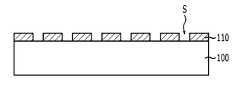
도 1a를 참조하면, 반도체 웨이퍼(100)의 전면 상에 반도체 칩(110)을 매트릭스(matrix) 배열을 이루도록 서로 일정 간격 이격시켜 형성한다. 또한, 반도체 웨이퍼(100)의 전면 상에는 각 반도체 칩(110)의 외곽을 둘러싸도록 일정 폭을 갖는 스크라이브 라인(scribe line)(S)이 형성된다. 반도체 칩(110)은 소정 기능을 수행하는 회로부(미도시)를 구비한다.Referring to FIG. 1A, the
도 1b를 참조하면, 반도체 칩(110)을 보호하도록 반도체 칩(110) 상에 보호 테이프(120)를 형성한다.Referring to FIG. 1B, a
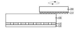
도 1c를 참조하면, 그라인더(200)에 메시수가 200 내지 400 가량인 그라인딩 휠(210)을 사용하여 러프(rough) 그라인딩 공정에 의해 반도체 웨이퍼(100)의 후면을 제1 그라인딩 한다.Referring to FIG. 1C, the back surface of the
도 1d를 참조하면, 그라인더(200)에 메시수가 2000 이상인 그라인딩 휠(220)을 사용하여 미세 그라인딩 공정에 의해 제1 그라인딩된 반도체 웨이퍼(100A)의 후면을 제2 그라인딩 한다.Referring to FIG. 1D, the back surface of the first
도 1e를 참조하면, 제2 그라인딩된 반도체 웨이퍼(100B)의 후면을 연마기(300)를 이용하여 건식 연마에 의해 연마하여, 그라인딩 공정들에서 반도체 웨이퍼(100B)의 후면에 발생된 기계적 결함 등을 제거함으로써 반도체 웨이퍼(100B) 후면의 스트레스를 완화시켜, 결함 등에 의해 반도체 칩(110)에 크랙이 발생되지 않도록 한다.Referring to FIG. 1E, the back surface of the second
도 1f를 참조하면, 연마된 반도체 웨이퍼(100C)의 후면에 다이싱/다이본드 시트(140)를 부착한다.Referring to FIG. 1F, a dicing /
여기서, 다이싱/다이본드 시트(140)는 기재(142) 및 기재(142) 상에 형성된 접착층(144)으로 이루어져 접착층(144)을 통해 반도체 웨이퍼(100C)에 부착된다.Here, the dicing /
도 1g에 나타낸 바와 같이, 보호 테이프(120)를 제거한 후, 도 1h에 나타낸 바와 같이, 블레이드(400)를 이용하여 반도체 웨이퍼(100C)의 스크라이브 라인(S)을 절단하여 반도체 칩(110)을 분리한다.As shown in FIG. 1G, after removing the
이와 같이 종래의 웨이퍼 가공 방법에서는 그라인딩 공정들을 수행한 후 연마를 수행하기 때문에 그라인딩 공정에 의해 웨이퍼(100B) 후면에 발생된 기계적 결함을 제거할 수 있었다.As described above, in the conventional wafer processing method, since grinding is performed after grinding processes, mechanical defects generated on the back surface of the
반면, 그라인딩 공정들에 의해 반도체 웨이퍼(100B) 후면에 발생된 기계적 결함은 이처럼 반도체 칩(110)의 크랙 문제를 유발하기도 하지만, 후속 패키지 공 정 중에 오염되는 금속 등의 불순물을 포획하는 EG(extrinsic gettering) 효과를 가지고 있다. 따라서, 연마 공정에 의해 기계적 결함을 완전히 제거하게 되면 EG 효과를 얻을 수 없어 패키지 공정 중 금속 등의 불순물에 의한 반도체 웨이퍼(100C)의 오염을 방지하기가 어렵다.On the other hand, mechanical defects generated on the back surface of the
이러한 웨이퍼(100C)에 잔존하는 금속 등의 불순물은 산화막 내압을 저하시키고 결정 결함 등을 유발할 뿐만 아니라 누설 전류를 증가시켜, 결국 디바이스의 수율 및 신뢰성을 저하시킨다.Impurities such as metal remaining in the
본 발명은 상기와 같은 종래기술의 문제점을 해결하기 위하여 제안된 것으로, 그라인딩 공정 후 발생되는 기계적 결함에 의한 반도체 칩의 크랙을 방지하면서 패키지 공정 중의 게터링 능력을 강화할 수 있는 웨이퍼 가공 방법을 제공하는데 그 목적이 있다.The present invention has been proposed to solve the above problems of the prior art, to provide a wafer processing method that can enhance the gettering capability during the packaging process while preventing cracking of the semiconductor chip due to mechanical defects generated after the grinding process. The purpose is.
상기의 기술적 과제를 달성하기 위한 본 발명의 일 측면에 따르면, 전면 상에 반도체 칩이 배열된 웨이퍼를 준비하는 단계; 반도체 칩 상에 보호 테이프를 형성하는 단계; 웨이퍼의 후면을 그라인딩하는 단계; 그라인딩된 웨이퍼의 후면을 연마하는 단계; 및 연마된 웨이퍼의 후면 표면 내에 금속 포획층을 형성하는 단계를 포함하는, 웨이퍼 가공 방법이 제공된다.According to an aspect of the present invention for achieving the above technical problem, preparing a wafer having a semiconductor chip arranged on the front surface; Forming a protective tape on the semiconductor chip; Grinding the back side of the wafer; Polishing the back side of the ground wafer; And forming a metal capture layer within the backside surface of the polished wafer.
여기서, 금속 포획층은 상기 웨이퍼의 후면의 표면으로부터 0.1 내지 수 ㎛의 깊이로 형성하는 것이 바람직하다.Here, the metal capture layer is preferably formed to a depth of 0.1 to several micrometers from the surface of the back surface of the wafer.
또한, 금속 포획층은 고농도의 보론 이온을 이온주입하여 형성할 수도 있고, 고농도의 As 이온을 이온주입하여 형성할 수도 있다.The metal capture layer may be formed by ion implantation of high concentration of boron ions, or may be formed by ion implantation of high concentration of As ions.
또한, 웨이퍼의 후면을 그라인딩 하는 단계는, 웨이퍼의 후면을 러프 그라인딩 공정에 의해 제1 그라인딩 하는 단계; 및 제1 그라인딩된 웨이퍼의 후면을 미세 그라인딩 공정에 의해 제2 그라인딩 하는 단계를 포함할 수도 있다.In addition, the grinding of the back surface of the wafer may include: first grinding the back surface of the wafer by a rough grinding process; And second grinding the back surface of the first ground wafer by a fine grinding process.
또한, 웨이퍼의 후면을 연마하는 단계는 건식 연마로 수행할 수도 있다.In addition, the polishing of the back surface of the wafer may be performed by dry polishing.
또한, 금속 포획층이 형성된 웨이퍼의 후면에 다이싱/다이본드 시트를 부착하는 단계; 보호 테이프를 제거하는 단계; 및 반도체 칩을 분리하는 단계를 더 포함할 수도 있다.In addition, attaching a dicing / die bond sheet to the back of the wafer on which the metal capture layer is formed; Removing the protective tape; And separating the semiconductor chip.
전술한 본 발명은, 그라인딩 공정들을 수행한 후 연마를 수행하여 그라인딩 공정에 의해 반도체 웨이퍼의 후면에 발생된 기계적 결함을 제거함으로써 반도체 칩의 크랙을 억제할 수 있다.According to the present invention described above, the grinding of the semiconductor chip can be suppressed by removing the mechanical defects generated on the back surface of the semiconductor wafer by the grinding process by performing grinding.
또한, 연마를 수행한 후 반도체 웨이퍼의 후면 표면 내에 고농도의 보론 이온 주입층으로 이루어진 금속 포획층을 형성하여 패키지 공정 중의 금속 등의 불순물에 대한 게터링 능력을 강화시킴으로써 산화막 내압 저하, 결정 결함 유발 및 누설 전류 증가 등의 문제를 방지할 수 있다.In addition, after polishing, a metal capture layer made of a high concentration of boron ion implantation layer is formed on the back surface of the semiconductor wafer to enhance gettering ability of impurities such as metal during the packaging process, thereby lowering the oxide pressure resistance and causing crystal defects. Problems such as an increase in leakage current can be prevented.
또한, 게터링 효과 강화를 위해 사용되는 P/P+ 에피층 구조의 웨이퍼 사용을 대체할 수 있다.It can also replace the use of wafers with P / P + epilayer structures used to enhance gettering effects.
그 결과, 반도체 디바이스의 수율 및 신뢰성을 개선할 수 있는 효과가 있다.As a result, there is an effect that can improve the yield and the reliability of the semiconductor device.
이하, 본 발명이 속한 기술분야에서 통상의 지식을 가진 자가 본 발명을 보다 용이하게 실시할 수 있도록 하기 위하여 본 발명의 실시예를 소개하기로 한다.Hereinafter, embodiments of the present invention will be introduced in order to enable those skilled in the art to more easily implement the present invention.
그러나, 본 발명의 실시예는 여러 가지 다른 형태로 변형될 수 있으며, 본 발명의 범위가 아래에서 상술하는 실시예로 한정되는 것으로 해석되어서는 안 된다. 또한, 도면에서 막 또는 영역들의 크기 또는 두께는 명세서의 명확성을 위하 여 과장된 것이며, 도면 상에서 동일한 부호로 표시된 요소는 동일한 요소를 의미한다.However, embodiments of the present invention may be modified in many different forms, and the scope of the present invention should not be construed as being limited to the embodiments described below. In addition, the size or thickness of the film or regions in the drawings are exaggerated for clarity of the specification, elements denoted by the same reference numerals in the drawings means the same element.
도 2a 내지 도 2i는 본 발명의 실시예에 따른 웨이퍼 가공 방법을 설명하기 위한 순차적 공정 단면도들이다.2A to 2I are sequential process cross-sectional views illustrating a wafer processing method according to an embodiment of the present invention.
도 2a를 참조하면, 반도체 웨이퍼(100)의 전면 상에 반도체 칩(110)을 매트릭스(matrix) 배열을 이루도록 서로 일정 간격 이격시켜 형성한다. 또한, 각 반도체 칩(110)의 외곽을 둘러싸도록 일정 폭을 갖는 스크라이브 라인(scribe line)(S)이 형성된다. 여기서, 반도체 칩(110)은 소정 기능을 수행하는 회로부(미도시)를 구비한다.Referring to FIG. 2A, the
도 2b를 참조하면, 반도체 칩(110)을 보호하도록 반도체 칩(110) 상에 보호 테이프(120)를 형성한다.Referring to FIG. 2B, a
도 2c를 참조하면, 그라인더(200)에 메시수가 200 내지 400 가량인 그라인딩 휠(210)을 사용하여 러프(rough) 그라인딩 공정에 의해 반도체 웨이퍼(100)의 후면을 제1 그라인딩 한다.Referring to FIG. 2C, the back surface of the
도 2d를 참조하면, 그라인더(200)에 메시수가 2000 이상인 그라인딩 휠(220)을 사용하여 미세 그라인딩 공정에 의해 제1 그라인딩된 반도체 웨이퍼(100A)의 후면을 제2 그라인딩 한다.Referring to FIG. 2D, the back surface of the first
도 2e를 참조하면, 제2 그라인딩된 반도체 웨이퍼(100B)의 후면을 연마기(300)를 이용하여 건식 연마에 의해 연마하여, 그라인딩 공정들에서 반도체 웨이퍼(100B)의 후면에 발생된 기계적 결함 등을 제거함으로써 반도체 웨이퍼(100B) 후 면의 스트레스를 완화시켜, 결함 등에 의해 반도체 칩(110)에 크랙이 발생되지 않도록 한다.Referring to FIG. 2E, the back surface of the second
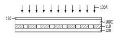
도 2f를 참조하면, 연마된 반도체 웨이퍼(100C)의 후면에 보론(B) 이온을 이온주입(130A)하여 반도체 웨이퍼(100C)의 후면 표면 내에 보론 이온주입층으로 이루어진 금속 포획층(130)을 형성한다.Referring to FIG. 2F, boron (B) ions are implanted into the back surface of the
이때, 금속 포획층(130)은 반도체 웨이퍼(100C)의 후면 표면으로부터 0.1 내지 수 ㎛의 깊이로 형성하는 것이 바람직하다.In this case, the
이와 같이, 반도체 웨이퍼(100C)의 후면 표면 내에 보론 이온주입층으로 이루어진 금속 포획층(130)이 형성되면, 반도체 웨이퍼(100C)가 금속 등의 불순물에 의해 오염되는 경우 금속 포획층(130)에 의해 금속 등의 불순물의 용해도가 증가되어 금속 포획층(130) 내로 확산되고, 여기서 세그리게이션(segregation)에 의한 게터링 효과가 발휘된다.As such, when the
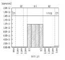
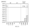
한편, 도 3a 및 도 3b는 반도체 웨이퍼(100C)의 후면에 보론 이온을 이온주입한 후의 반도체 웨이퍼(100C) 내의 불순물 농도 프로파일을 나타낸 도면으로서, 도 3a는 이온주입 직후의 보론 농도 분포를 나타내고, 도 3b는 통상의 열처리 공정을 수행한 후의 보론의 농도 분포를 나타낸 것으로, 보론 이온의 농도가 높을수록(G2) 열처리 후에도 반도체 웨이퍼(100C)에 더 높은 농도로 더 깊게 분포하게 되어 세그리게이션 게터링 효과가 더 높게 발휘됨을 알 수 있다.3A and 3B are diagrams showing impurity concentration profiles in the
또한, 도 4a 내지 도 4c는 반도체 웨이퍼 내에서의 Cu 게터링 능력을 나타낸 도면으로서, 도 4a는 반도체 웨이퍼의 후면에 금속 포획층(130)이 형성되지 않은 경우의 Cu 게터링 능력을 나타내고, 도 4b 및 도 4c는 모두 반도체 웨이퍼(100C)의 후면에 금속 포획층(130)이 형성된 경우의 Cu 게터링 능력을 나타낸 것으로, 도 4b의 경우가 도 4a의 경우보다 금속 포획층(130)의 보론 이온의 농도가 높은 경우를 나타낸다. 도 4a의 경우에는 대부분의 Cu가 반도체 웨이퍼의 후면 및 전면으로부터 약 2㎛ 이상의 깊이 이내의 벌크 내에 존재하고, 도 4b 및 도 4c의 경우 반도체 웨이퍼 후면의 금속 포획층(130) 주위에서 대부분의 Cu가 존재하지만, 특히 도 4c의 경우 금속 포획층(130) 위치에서 대부분의 Cu가 존재함을 알 수 있다.4A to 4C show the Cu gettering capability in the semiconductor wafer, and FIG. 4A shows the Cu gettering capability when the
따라서, 금속 포획층(130) 형성을 위한 보론 이온의 이온 주입시 보론 이온의 농도는, 비교적 고농도로, 바람직하게 6E15 atoms/㎠ 이상으로 조절하는 것이 바람직하다.Therefore, the concentration of the boron ions at the time of ion implantation of the boron ions for forming the
도 2g를 참조하면, 금속 포획층(130)이 형성된 반도체 웨이퍼(100C)의 후면에 다이싱/다이본드 시트(140)를 부착한다.Referring to FIG. 2G, the dicing / die
여기서, 다이싱/다이본드 시트(140)는 기재(142) 및 기재(142) 상에 형성된 접착층(144)으로 이루어져 접착층(144)을 통해 반도체 웨이퍼(100C)에 부착된다.Here, the dicing / die
도 2h에 나타낸 바와 같이, 보호 테이프(120)를 제거한 후, 도 2i에 나타낸 바와 같이, 블레이드(400)를 이용하여 반도체 웨이퍼(100C)의 스크라이브 라인(S)을 절단하여 반도체 칩(110)을 분리한다.As shown in FIG. 2H, after removing the
상기 실시예에 의하면, 그라인딩 공정들을 수행한 후 연마를 수행하여 그라인딩 공정에 의해 반도체 웨이퍼(100B)의 후면에 발생된 기계적 결함을 제거함으로써 반도체 칩(110)의 크랙을 억제할 수 있다.According to the above embodiment, the grinding of the
또한 연마를 수행한 후 반도체 웨이퍼(100C)의 후면 표면 내에 고농도의 보론 이온 주입층으로 이루어진 금속 포획층(130)을 형성하여 패키지 공정 중의 금속 등의 불순물에 대한 게터링 능력을 강화시킴으로써, 산화막 내압 저하, 결정 결함 유발 및 누설 전류 증가 등의 문제를 방지할 수 있다.In addition, after polishing, a
또한, 게터링 효과 강화를 위해 사용되는 P/P+ 에피층 구조의 웨이퍼 사용을 대체할 수 있다.It can also replace the use of wafers with P / P + epilayer structures used to enhance gettering effects.
그 결과, 반도체 디바이스의 수율 및 신뢰성을 개선할 수 있다.As a result, the yield and reliability of the semiconductor device can be improved.
본 발명의 기술 사상은 상기 실시예에 따라 구체적으로 기술되었으나, 상기한 실시예는 그 설명을 위한 것이며 그 제한을 위한 것이 아님을 주의하여야 한다. 또한, 본 발명의 기술 분야의 통상의 전문가라면 본 발명의 기술 사상의 범위 내에서 다양한 실시예가 가능함을 이해할 수 있을 것이다.Although the technical spirit of the present invention has been described in detail according to the above embodiments, it should be noted that the above embodiments are for the purpose of description and not of limitation. In addition, those skilled in the art will understand that various embodiments are possible within the scope of the technical idea of the present invention.
예컨대, 전술한 실시예에서는 금속 포획층으로서 보론 이온과 같은 P형 불순물이 고농도로 이온주입되어 형성되었지만, 보론 대신에 As 이온과 같은 N형 불순물이 사용될 수도 있다.For example, in the above embodiment, P-type impurities such as boron ions are formed by ion implantation at high concentration as the metal capture layer, but N-type impurities such as As ions may be used instead of boron.
도 1a 내지 도 1h는 종래의 웨이퍼 가공 방법을 설명하기 위한 순차적 공정 단면도.1A to 1H are sequential process cross-sectional views for explaining a conventional wafer processing method.
도 2a 내지 도 2i는 본 발명의 실시예에 따른 웨이퍼 가공 방법을 설명하기 위한 순차적 공정 단면도.2A to 2I are sequential process cross-sectional views for explaining a wafer processing method according to an embodiment of the present invention.
도 3a 및 도 3b는 반도체 웨이퍼의 후면에 보론 이온을 이온주입한 후의 반도체 웨이퍼 내의 불순물 농도 프로파일을 나타낸 도면으로서, 도 3a는 이온주입 직후의 보론 농도 분포를 나타내고, 도 3b는 통상의 열처리 공정을 수행한 후의 보론의 농도 분포를 나타냄.3A and 3B show an impurity concentration profile in a semiconductor wafer after ion implantation of boron ions on a back surface of the semiconductor wafer. FIG. 3A shows a boron concentration distribution immediately after ion implantation, and FIG. 3B shows a conventional heat treatment process. Shows the concentration distribution of boron after execution.
도 4a 내지 도 4c는 반도체 웨이퍼 내에서의 Cu 게터링 능력을 나타낸 도면으로서, 도 4a는 반도체 웨이퍼의 후면에 금속 포획층이 형성되지 않은 경우를 나타낸 것으로, 도 4b 및 도 4c는 모두 반도체 웨이퍼의 후면에 금속 포획층이 형성된 경우이며, 도 4b의 경우가 도 4a의 경우보다 금속 포획층의 보론 이온의 농도가 높음.4A to 4C are diagrams showing Cu gettering capability in a semiconductor wafer, and FIG. 4A shows a case in which a metal capture layer is not formed on a rear surface of a semiconductor wafer. FIGS. 4B and 4C are both diagrams of a semiconductor wafer. The metal capture layer is formed on the back surface, and the concentration of boron ions in the metal capture layer is higher in the case of FIG. 4B than in FIG. 4A.
* 도면의 주요 부분에 대한 부호의 설명* Explanation of symbols for the main parts of the drawings
100, 100A, 100B, 100C : 반도체 웨이퍼100, 100A, 100B, 100C: semiconductor wafer
110 : 반도체 칩110: semiconductor chip
120 : 보호 테이프120: protective tape
130 : 금속 포획층130: metal capture layer
140 : 다이싱/다이 본드 시트140: dicing / die bond sheet
142 : 기재142: description
144 : 접착층144: adhesive layer
200 : 그라인더200 grinder
210, 220 : 그라인딩 휠210, 220: Grinding Wheel
300 : 연마기300: grinding machine
S : 스크라이브 라인S: scribe line
400 : 블레이드400: blade
Claims (7)
Translated fromKoreanPriority Applications (1)
| Application Number | Priority Date | Filing Date | Title |
|---|---|---|---|
| KR1020090134083AKR20110077485A (en) | 2009-12-30 | 2009-12-30 | Wafer processing method |
Applications Claiming Priority (1)
| Application Number | Priority Date | Filing Date | Title |
|---|---|---|---|
| KR1020090134083AKR20110077485A (en) | 2009-12-30 | 2009-12-30 | Wafer processing method |
Publications (1)
| Publication Number | Publication Date |
|---|---|
| KR20110077485Atrue KR20110077485A (en) | 2011-07-07 |
Family
ID=44917072
Family Applications (1)
| Application Number | Title | Priority Date | Filing Date |
|---|---|---|---|
| KR1020090134083AWithdrawnKR20110077485A (en) | 2009-12-30 | 2009-12-30 | Wafer processing method |
Country Status (1)
| Country | Link |
|---|---|
| KR (1) | KR20110077485A (en) |
Cited By (4)
| Publication number | Priority date | Publication date | Assignee | Title |
|---|---|---|---|---|
| US8866269B2 (en) | 2012-07-16 | 2014-10-21 | SK Hynix Inc. | Semiconductor chips having improved solidity, semiconductor packages including the same and methods of fabricating the same |
| KR20160067334A (en) | 2014-12-04 | 2016-06-14 | 주식회사 포스코 | Spray apparatus |
| US9589842B2 (en) | 2015-01-30 | 2017-03-07 | Samsung Electronics Co., Ltd. | Semiconductor package and method of fabricating the same |
| KR20180123434A (en)* | 2017-05-08 | 2018-11-16 | 가부시기가이샤 디스코 | Method for forming gettering layer |
- 2009
- 2009-12-30KRKR1020090134083Apatent/KR20110077485A/ennot_activeWithdrawn
Cited By (5)
| Publication number | Priority date | Publication date | Assignee | Title |
|---|---|---|---|---|
| US8866269B2 (en) | 2012-07-16 | 2014-10-21 | SK Hynix Inc. | Semiconductor chips having improved solidity, semiconductor packages including the same and methods of fabricating the same |
| US9324686B2 (en) | 2012-07-16 | 2016-04-26 | SK Hynix Inc. | Semiconductor chips having improved solidity, semiconductor packages including the same and methods of fabricating the same |
| KR20160067334A (en) | 2014-12-04 | 2016-06-14 | 주식회사 포스코 | Spray apparatus |
| US9589842B2 (en) | 2015-01-30 | 2017-03-07 | Samsung Electronics Co., Ltd. | Semiconductor package and method of fabricating the same |
| KR20180123434A (en)* | 2017-05-08 | 2018-11-16 | 가부시기가이샤 디스코 | Method for forming gettering layer |
Similar Documents
| Publication | Publication Date | Title |
|---|---|---|
| KR102320674B1 (en) | Processed stacked dies | |
| KR101469331B1 (en) | Scribe lines in wafers | |
| CN103035571B (en) | For the method for testing of semiconductor device | |
| TW201314757A (en) | Dicing before grinding after coating | |
| US9070672B2 (en) | Semiconductor device packaging structure and packaging method | |
| US7846776B2 (en) | Methods for releasably attaching sacrificial support members to microfeature workpieces and microfeature devices formed using such methods | |
| US20060022321A1 (en) | Semiconductor chip having gettering layer, and method for manufacturing the same | |
| TW201126648A (en) | Semiconductor die singulation method | |
| US12424574B2 (en) | Polymer coated semiconductor devices and hybrid bonding to form semiconductor assemblies | |
| US9917011B2 (en) | Semiconductor wafer, semiconductor device diced from semiconductor wafer, and method for manufacturing semiconductor device | |
| KR20140018226A (en) | Pre-cut wafer applied underfill film | |
| CN102693941A (en) | Wafer cutting process | |
| KR20110077485A (en) | Wafer processing method | |
| JP2012064656A (en) | Manufacturing method of semiconductor device | |
| CN106796874B (en) | Manufacturing method of semiconductor device | |
| US7659140B2 (en) | Integrated circuit system with a debris trapping system | |
| US8993412B1 (en) | Method for reducing backside die damage during die separation process | |
| US20170154853A1 (en) | Method for singulating a multiplicity of chips | |
| US8765527B1 (en) | Semiconductor device with redistributed contacts | |
| KR100954921B1 (en) | Back metal layer filling test method for vertical semiconductor devices | |
| JP4724729B2 (en) | Manufacturing method of semiconductor device | |
| JP5470766B2 (en) | Manufacturing method of semiconductor device | |
| JP2009295766A (en) | Method of manufacturing semiconductor device | |
| JP2004186442A (en) | Method for manufacturing power semiconductor chip | |
| JP2003303790A (en) | Semiconductor wafer |
Legal Events
| Date | Code | Title | Description |
|---|---|---|---|
| PA0109 | Patent application | Patent event code:PA01091R01D Comment text:Patent Application Patent event date:20091230 | |
| PG1501 | Laying open of application | ||
| PC1203 | Withdrawal of no request for examination | ||
| WITN | Application deemed withdrawn, e.g. because no request for examination was filed or no examination fee was paid |