KR20110059724A - Laser material removal method and apparatus - Google Patents
Laser material removal method and apparatusDownload PDFInfo
- Publication number
- KR20110059724A KR20110059724AKR1020117006576AKR20117006576AKR20110059724AKR 20110059724 AKR20110059724 AKR 20110059724AKR 1020117006576 AKR1020117006576 AKR 1020117006576AKR 20117006576 AKR20117006576 AKR 20117006576AKR 20110059724 AKR20110059724 AKR 20110059724A
- Authority
- KR
- South Korea
- Prior art keywords
- substrate
- dielectric layer
- laser scanner
- laser
- robot
- Prior art date
- Legal status (The legal status is an assumption and is not a legal conclusion. Google has not performed a legal analysis and makes no representation as to the accuracy of the status listed.)
- Withdrawn
Links
- 238000000034methodMethods0.000titleclaimsabstractdescription53
- 239000000463materialSubstances0.000titleclaimsabstractdescription30
- 239000000758substrateSubstances0.000claimsabstractdescription361
- 238000000151depositionMethods0.000claimsabstractdescription36
- 238000012546transferMethods0.000claimsdescription71
- 230000008021depositionEffects0.000claimsdescription30
- 238000012545processingMethods0.000claimsdescription21
- 239000003989dielectric materialSubstances0.000claimsdescription16
- 238000001704evaporationMethods0.000claimsdescription16
- 238000003672processing methodMethods0.000claims4
- 230000008646thermal stressEffects0.000abstractdescription8
- 238000004519manufacturing processMethods0.000abstractdescription6
- 238000005286illuminationMethods0.000description28
- 238000007689inspectionMethods0.000description26
- VYPSYNLAJGMNEJ-UHFFFAOYSA-NSilicium dioxideChemical compoundO=[Si]=OVYPSYNLAJGMNEJ-UHFFFAOYSA-N0.000description15
- 238000005240physical vapour depositionMethods0.000description12
- 230000008020evaporationEffects0.000description11
- 238000010586diagramMethods0.000description10
- 229910052814silicon oxideInorganic materials0.000description9
- 238000000059patterningMethods0.000description8
- 229910052581Si3N4Inorganic materials0.000description7
- HQVNEWCFYHHQES-UHFFFAOYSA-Nsilicon nitrideChemical compoundN12[Si]34N5[Si]62N3[Si]51N64HQVNEWCFYHHQES-UHFFFAOYSA-N0.000description7
- PXHVJJICTQNCMI-UHFFFAOYSA-NNickelChemical compound[Ni]PXHVJJICTQNCMI-UHFFFAOYSA-N0.000description6
- 238000000608laser ablationMethods0.000description6
- 238000005259measurementMethods0.000description6
- 238000000623plasma-assisted chemical vapour depositionMethods0.000description6
- 230000004044responseEffects0.000description6
- 239000007787solidSubstances0.000description6
- 229910052710siliconInorganic materials0.000description5
- 239000010703siliconSubstances0.000description5
- XUIMIQQOPSSXEZ-UHFFFAOYSA-NSiliconChemical compound[Si]XUIMIQQOPSSXEZ-UHFFFAOYSA-N0.000description4
- 229910052782aluminiumInorganic materials0.000description4
- XAGFODPZIPBFFR-UHFFFAOYSA-NaluminiumChemical compound[Al]XAGFODPZIPBFFR-UHFFFAOYSA-N0.000description4
- 229910021417amorphous siliconInorganic materials0.000description4
- JBRZTFJDHDCESZ-UHFFFAOYSA-NAsGaChemical compound[As]#[Ga]JBRZTFJDHDCESZ-UHFFFAOYSA-N0.000description3
- KTSFMFGEAAANTF-UHFFFAOYSA-N[Cu].[Se].[Se].[In]Chemical compound[Cu].[Se].[Se].[In]KTSFMFGEAAANTF-UHFFFAOYSA-N0.000description3
- 230000003667anti-reflective effectEffects0.000description3
- 238000005229chemical vapour depositionMethods0.000description3
- 239000010949copperSubstances0.000description3
- 230000003287optical effectEffects0.000description3
- 230000002093peripheral effectEffects0.000description3
- 235000012239silicon dioxideNutrition0.000description3
- 239000000377silicon dioxideSubstances0.000description3
- WUPHOULIZUERAE-UHFFFAOYSA-N3-(oxolan-2-yl)propanoic acidChemical compoundOC(=O)CCC1CCCO1WUPHOULIZUERAE-UHFFFAOYSA-N0.000description2
- MARUHZGHZWCEQU-UHFFFAOYSA-N5-phenyl-2h-tetrazoleChemical compoundC1=CC=CC=C1C1=NNN=N1MARUHZGHZWCEQU-UHFFFAOYSA-N0.000description2
- RYGMFSIKBFXOCR-UHFFFAOYSA-NCopperChemical compound[Cu]RYGMFSIKBFXOCR-UHFFFAOYSA-N0.000description2
- 229910001218Gallium arsenideInorganic materials0.000description2
- BQCADISMDOOEFD-UHFFFAOYSA-NSilverChemical compound[Ag]BQCADISMDOOEFD-UHFFFAOYSA-N0.000description2
- ATJFFYVFTNAWJD-UHFFFAOYSA-NTinChemical compound[Sn]ATJFFYVFTNAWJD-UHFFFAOYSA-N0.000description2
- 229910052980cadmium sulfideInorganic materials0.000description2
- 229910017052cobaltInorganic materials0.000description2
- 239000010941cobaltSubstances0.000description2
- GUTLYIVDDKVIGB-UHFFFAOYSA-Ncobalt atomChemical compound[Co]GUTLYIVDDKVIGB-UHFFFAOYSA-N0.000description2
- 229910052802copperInorganic materials0.000description2
- 238000013461designMethods0.000description2
- 230000005611electricityEffects0.000description2
- 229910052751metalInorganic materials0.000description2
- 239000002184metalSubstances0.000description2
- 150000002739metalsChemical class0.000description2
- 229910052759nickelInorganic materials0.000description2
- HBVFXTAPOLSOPB-UHFFFAOYSA-Nnickel vanadiumChemical compound[V].[Ni]HBVFXTAPOLSOPB-UHFFFAOYSA-N0.000description2
- 230000003647oxidationEffects0.000description2
- 238000007254oxidation reactionMethods0.000description2
- 238000002161passivationMethods0.000description2
- 229910021420polycrystalline siliconInorganic materials0.000description2
- 229910052702rheniumInorganic materials0.000description2
- WUAPFZMCVAUBPE-UHFFFAOYSA-Nrhenium atomChemical compound[Re]WUAPFZMCVAUBPE-UHFFFAOYSA-N0.000description2
- 229910052709silverInorganic materials0.000description2
- 239000004332silverSubstances0.000description2
- 239000007921spraySubstances0.000description2
- 230000035882stressEffects0.000description2
- JBQYATWDVHIOAR-UHFFFAOYSA-NtellanylidenegermaniumChemical compound[Te]=[Ge]JBQYATWDVHIOAR-UHFFFAOYSA-N0.000description2
- GYHNNYVSQQEPJS-UHFFFAOYSA-NGalliumChemical compound[Ga]GYHNNYVSQQEPJS-UHFFFAOYSA-N0.000description1
- GPXJNWSHGFTCBW-UHFFFAOYSA-NIndium phosphideChemical compound[In]#PGPXJNWSHGFTCBW-UHFFFAOYSA-N0.000description1
- 238000000137annealingMethods0.000description1
- 238000000429assemblyMethods0.000description1
- 230000000712assemblyEffects0.000description1
- 238000001505atmospheric-pressure chemical vapour depositionMethods0.000description1
- 238000004891communicationMethods0.000description1
- 239000004020conductorSubstances0.000description1
- 239000013078crystalSubstances0.000description1
- 238000005137deposition processMethods0.000description1
- 238000009792diffusion processMethods0.000description1
- 238000009826distributionMethods0.000description1
- 239000000835fiberSubstances0.000description1
- 239000012530fluidSubstances0.000description1
- 229910052733galliumInorganic materials0.000description1
- 229910052732germaniumInorganic materials0.000description1
- GNPVGFCGXDBREM-UHFFFAOYSA-Ngermanium atomChemical compound[Ge]GNPVGFCGXDBREM-UHFFFAOYSA-N0.000description1
- 238000011068loading methodMethods0.000description1
- 238000004518low pressure chemical vapour depositionMethods0.000description1
- 229910021421monocrystalline siliconInorganic materials0.000description1
- 239000011368organic materialSubstances0.000description1
- 238000002360preparation methodMethods0.000description1
- 230000001902propagating effectEffects0.000description1
- 238000007650screen-printingMethods0.000description1
- SBIBMFFZSBJNJF-UHFFFAOYSA-Nselenium;zincChemical compound[Se]=[Zn]SBIBMFFZSBJNJF-UHFFFAOYSA-N0.000description1
- HBMJWWWQQXIZIP-UHFFFAOYSA-Nsilicon carbideChemical compound[Si+]#[C-]HBMJWWWQQXIZIP-UHFFFAOYSA-N0.000description1
- 229910010271silicon carbideInorganic materials0.000description1
- 238000003860storageMethods0.000description1
- 239000012808vapor phaseSubstances0.000description1
Images


Classifications
- B—PERFORMING OPERATIONS; TRANSPORTING
- B23—MACHINE TOOLS; METAL-WORKING NOT OTHERWISE PROVIDED FOR
- B23K—SOLDERING OR UNSOLDERING; WELDING; CLADDING OR PLATING BY SOLDERING OR WELDING; CUTTING BY APPLYING HEAT LOCALLY, e.g. FLAME CUTTING; WORKING BY LASER BEAM
- B23K26/00—Working by laser beam, e.g. welding, cutting or boring
- B23K26/02—Positioning or observing the workpiece, e.g. with respect to the point of impact; Aligning, aiming or focusing the laser beam
- B23K26/03—Observing, e.g. monitoring, the workpiece
- B—PERFORMING OPERATIONS; TRANSPORTING
- B23—MACHINE TOOLS; METAL-WORKING NOT OTHERWISE PROVIDED FOR
- B23K—SOLDERING OR UNSOLDERING; WELDING; CLADDING OR PLATING BY SOLDERING OR WELDING; CUTTING BY APPLYING HEAT LOCALLY, e.g. FLAME CUTTING; WORKING BY LASER BEAM
- B23K26/00—Working by laser beam, e.g. welding, cutting or boring
- B23K26/02—Positioning or observing the workpiece, e.g. with respect to the point of impact; Aligning, aiming or focusing the laser beam
- B23K26/06—Shaping the laser beam, e.g. by masks or multi-focusing
- B23K26/062—Shaping the laser beam, e.g. by masks or multi-focusing by direct control of the laser beam
- B23K26/0622—Shaping the laser beam, e.g. by masks or multi-focusing by direct control of the laser beam by shaping pulses
- B23K26/0624—Shaping the laser beam, e.g. by masks or multi-focusing by direct control of the laser beam by shaping pulses using ultrashort pulses, i.e. pulses of 1ns or less
- B—PERFORMING OPERATIONS; TRANSPORTING
- B23—MACHINE TOOLS; METAL-WORKING NOT OTHERWISE PROVIDED FOR
- B23K—SOLDERING OR UNSOLDERING; WELDING; CLADDING OR PLATING BY SOLDERING OR WELDING; CUTTING BY APPLYING HEAT LOCALLY, e.g. FLAME CUTTING; WORKING BY LASER BEAM
- B23K26/00—Working by laser beam, e.g. welding, cutting or boring
- B23K26/08—Devices involving relative movement between laser beam and workpiece
- B23K26/082—Scanning systems, i.e. devices involving movement of the laser beam relative to the laser head
- B—PERFORMING OPERATIONS; TRANSPORTING
- B23—MACHINE TOOLS; METAL-WORKING NOT OTHERWISE PROVIDED FOR
- B23K—SOLDERING OR UNSOLDERING; WELDING; CLADDING OR PLATING BY SOLDERING OR WELDING; CUTTING BY APPLYING HEAT LOCALLY, e.g. FLAME CUTTING; WORKING BY LASER BEAM
- B23K26/00—Working by laser beam, e.g. welding, cutting or boring
- B23K26/08—Devices involving relative movement between laser beam and workpiece
- B23K26/083—Devices involving movement of the workpiece in at least one axial direction
- B23K26/0853—Devices involving movement of the workpiece in at least in two axial directions, e.g. in a plane
- B—PERFORMING OPERATIONS; TRANSPORTING
- B23—MACHINE TOOLS; METAL-WORKING NOT OTHERWISE PROVIDED FOR
- B23K—SOLDERING OR UNSOLDERING; WELDING; CLADDING OR PLATING BY SOLDERING OR WELDING; CUTTING BY APPLYING HEAT LOCALLY, e.g. FLAME CUTTING; WORKING BY LASER BEAM
- B23K26/00—Working by laser beam, e.g. welding, cutting or boring
- B23K26/36—Removing material
- B23K26/362—Laser etching
- B23K26/364—Laser etching for making a groove or trench, e.g. for scribing a break initiation groove
- B—PERFORMING OPERATIONS; TRANSPORTING
- B23—MACHINE TOOLS; METAL-WORKING NOT OTHERWISE PROVIDED FOR
- B23K—SOLDERING OR UNSOLDERING; WELDING; CLADDING OR PLATING BY SOLDERING OR WELDING; CUTTING BY APPLYING HEAT LOCALLY, e.g. FLAME CUTTING; WORKING BY LASER BEAM
- B23K26/00—Working by laser beam, e.g. welding, cutting or boring
- B23K26/36—Removing material
- B23K26/40—Removing material taking account of the properties of the material involved
- H—ELECTRICITY
- H10—SEMICONDUCTOR DEVICES; ELECTRIC SOLID-STATE DEVICES NOT OTHERWISE PROVIDED FOR
- H10F—INORGANIC SEMICONDUCTOR DEVICES SENSITIVE TO INFRARED RADIATION, LIGHT, ELECTROMAGNETIC RADIATION OF SHORTER WAVELENGTH OR CORPUSCULAR RADIATION
- H10F10/00—Individual photovoltaic cells, e.g. solar cells
- H10F10/10—Individual photovoltaic cells, e.g. solar cells having potential barriers
- H10F10/14—Photovoltaic cells having only PN homojunction potential barriers
- H10F10/146—Back-junction photovoltaic cells, e.g. having interdigitated base-emitter regions on the back side
- H—ELECTRICITY
- H10—SEMICONDUCTOR DEVICES; ELECTRIC SOLID-STATE DEVICES NOT OTHERWISE PROVIDED FOR
- H10F—INORGANIC SEMICONDUCTOR DEVICES SENSITIVE TO INFRARED RADIATION, LIGHT, ELECTROMAGNETIC RADIATION OF SHORTER WAVELENGTH OR CORPUSCULAR RADIATION
- H10F19/00—Integrated devices, or assemblies of multiple devices, comprising at least one photovoltaic cell covered by group H10F10/00, e.g. photovoltaic modules
- H—ELECTRICITY
- H10—SEMICONDUCTOR DEVICES; ELECTRIC SOLID-STATE DEVICES NOT OTHERWISE PROVIDED FOR
- H10F—INORGANIC SEMICONDUCTOR DEVICES SENSITIVE TO INFRARED RADIATION, LIGHT, ELECTROMAGNETIC RADIATION OF SHORTER WAVELENGTH OR CORPUSCULAR RADIATION
- H10F71/00—Manufacture or treatment of devices covered by this subclass
- H—ELECTRICITY
- H10—SEMICONDUCTOR DEVICES; ELECTRIC SOLID-STATE DEVICES NOT OTHERWISE PROVIDED FOR
- H10F—INORGANIC SEMICONDUCTOR DEVICES SENSITIVE TO INFRARED RADIATION, LIGHT, ELECTROMAGNETIC RADIATION OF SHORTER WAVELENGTH OR CORPUSCULAR RADIATION
- H10F77/00—Constructional details of devices covered by this subclass
- H10F77/20—Electrodes
- H10F77/206—Electrodes for devices having potential barriers
- H10F77/211—Electrodes for devices having potential barriers for photovoltaic cells
- H10F77/219—Arrangements for electrodes of back-contact photovoltaic cells
- B—PERFORMING OPERATIONS; TRANSPORTING
- B23—MACHINE TOOLS; METAL-WORKING NOT OTHERWISE PROVIDED FOR
- B23K—SOLDERING OR UNSOLDERING; WELDING; CLADDING OR PLATING BY SOLDERING OR WELDING; CUTTING BY APPLYING HEAT LOCALLY, e.g. FLAME CUTTING; WORKING BY LASER BEAM
- B23K2101/00—Articles made by soldering, welding or cutting
- B23K2101/36—Electric or electronic devices
- B23K2101/40—Semiconductor devices
- B—PERFORMING OPERATIONS; TRANSPORTING
- B23—MACHINE TOOLS; METAL-WORKING NOT OTHERWISE PROVIDED FOR
- B23K—SOLDERING OR UNSOLDERING; WELDING; CLADDING OR PLATING BY SOLDERING OR WELDING; CUTTING BY APPLYING HEAT LOCALLY, e.g. FLAME CUTTING; WORKING BY LASER BEAM
- B23K2103/00—Materials to be soldered, welded or cut
- B23K2103/50—Inorganic material, e.g. metals, not provided for in B23K2103/02 – B23K2103/26
- Y—GENERAL TAGGING OF NEW TECHNOLOGICAL DEVELOPMENTS; GENERAL TAGGING OF CROSS-SECTIONAL TECHNOLOGIES SPANNING OVER SEVERAL SECTIONS OF THE IPC; TECHNICAL SUBJECTS COVERED BY FORMER USPC CROSS-REFERENCE ART COLLECTIONS [XRACs] AND DIGESTS
- Y02—TECHNOLOGIES OR APPLICATIONS FOR MITIGATION OR ADAPTATION AGAINST CLIMATE CHANGE
- Y02E—REDUCTION OF GREENHOUSE GAS [GHG] EMISSIONS, RELATED TO ENERGY GENERATION, TRANSMISSION OR DISTRIBUTION
- Y02E10/00—Energy generation through renewable energy sources
- Y02E10/50—Photovoltaic [PV] energy
- Y02E10/547—Monocrystalline silicon PV cells
Landscapes
- Physics & Mathematics (AREA)
- Optics & Photonics (AREA)
- Engineering & Computer Science (AREA)
- Mechanical Engineering (AREA)
- Plasma & Fusion (AREA)
- Chemical & Material Sciences (AREA)
- Inorganic Chemistry (AREA)
- Laser Beam Processing (AREA)
- Container, Conveyance, Adherence, Positioning, Of Wafer (AREA)
- Photovoltaic Devices (AREA)
- Physical Vapour Deposition (AREA)
- Drying Of Semiconductors (AREA)
Abstract
Translated fromKorean
Description
Translated fromKorean본 발명의 실시예는 일반적으로 광전지(photovoltaic cells)의 제조에 관한 것이다. 특히, 본 발명의 실시예는 희망 패턴에 따라 재료 층의 일부를 레이저 제거하는 장치 및 방법에 관한 것이다.
Embodiments of the present invention generally relate to the manufacture of photovoltaic cells. In particular, embodiments of the present invention relate to an apparatus and method for laser removing a portion of a material layer in accordance with a desired pattern.
태양 전지는 태양 광을 직접적으로 전력으로 전환시키는 광기전성(PV) 장치이다. 가장 일반적인 태양 전지 재료는 실리콘이며, 때때로 웨이퍼로 지칭되는 단결정 또는 멀티 크리스탈(multicrystalline) 기판의 형태이다. 전기를 발생시키기 위해 실리콘 기반 태양 전지를 형성하는 감가상각 비용은 전통적인 방법을 사용하여 전기를 발생시키는 비용보다 일반적으로 더 높기 때문에, 태양 전지를 형성하는 비용을 감소시키는 것이 바람직하다.Solar cells are photovoltaic (PV) devices that convert sunlight directly into power. The most common solar cell material is silicon and is in the form of a single crystal or multicrystalline substrate, sometimes referred to as a wafer. Since the depreciation cost of forming silicon-based solar cells to generate electricity is generally higher than the cost of generating electricity using traditional methods, it is desirable to reduce the cost of forming solar cells.
다양한 방법으로 태양 전지의 전도체, 부동화 영역(passivation regions) 및 활성 영역(active regions)을 제조할 수 있다. 그러나 이러한 종래의 제조 방법 및 장치에는 몇몇 문제점이 존재한다. 예를 들면, 태양 전지 제조 중에 유전체 층 및 전도성 층의 일부를 레이저 제거하도록 제공하는 현행 방법은 시간 소모적이며 기저 기판을 손상시키게 될 수 있다.Various methods can be used to prepare the conductors, passivation regions and active regions of the solar cell. However, there are some problems with this conventional manufacturing method and apparatus. For example, current methods of providing for laser removal of portions of the dielectric and conductive layers during solar cell manufacturing are time consuming and can damage the underlying substrate.
따라서, 태양 전지의 제조중에 기판 수율을 향상시키고 층의 일부를 제거하는 향상된 레이저 제거 기술 및 장치가 필요하다.
Thus, there is a need for improved laser removal techniques and devices that improve substrate yield and remove portions of layers during the manufacture of solar cells.
본 발명의 일 실시예에서, 재료 제거를 위한 장치는 제1 표면상에 유전체 층이 증착되는 기판을 입력 영역으로부터 기판 이송 표면상의 복수의 지지 피처 중 하나로 이송하도록 구성되는 제1 로봇; 상기 기판의 실제 위치를 탐지하고, 상기 실제 위치에 관한 정보를 시스템 제어기로 전달하도록(communicate) 구성되는 비전 시스템(vision system); 상기 유전체 층의 일부를 희망 패턴으로 제거하도록 위치되는 제1 레이저 스캐너; 및 상기 제1 레이저 스캐너로부터 상기 유전체 층 위에 전도성 층을 증착하도록 구성되는 증착 챔버로 패터닝된 유전체 층을 갖는 기판을 이송하도록 구성되는 자동화 시스템을 포함한다. 일 실시예에서, 상기 시스템 제어기는 상기 기판의 예상 위치에 대한 상기 실제 위치의 오프셋을 결정하고 상기 오프셋을 수정하도록 상기 레이저 스캐너 또는 상기 제1 로봇을 조정하도록 구성된다.In one embodiment of the invention, an apparatus for material removal comprises: a first robot configured to transfer a substrate on which a dielectric layer is deposited onto a first surface from an input region to one of a plurality of support features on a substrate transfer surface; A vision system configured to detect an actual position of the substrate and communicate information about the actual position to a system controller; A first laser scanner positioned to remove a portion of the dielectric layer in a desired pattern; And an automation system configured to transfer the substrate having the patterned dielectric layer from the first laser scanner to a deposition chamber configured to deposit a conductive layer over the dielectric layer. In one embodiment, the system controller is configured to determine the offset of the actual position relative to the expected position of the substrate and to adjust the laser scanner or the first robot to correct the offset.
다른 실시예에서, 레이저 재료 제거 방법은 기판상에 증착된 재료의 레이저 제거 임계값(laser ablation threshold)을 결정하는 단계, 레이저로부터 방출된 빛의 일부가 상기 제거 임계값 아래에서 상기 기판에 부딪히도록 레이저를 탈초점시킴으로써(defocusing) 레이저의 파라미터 또는 기판의 위치를 변경하는 단계, 및 기저 기판을 손상시키지 않고 재료를 제거하는 단계를 포함한다.In another embodiment, a method of laser material removal comprises determining a laser ablation threshold of material deposited on a substrate, such that a portion of the light emitted from the laser strikes the substrate below the removal threshold. Changing the parameters of the laser or the position of the substrate by defocusing the laser, and removing the material without damaging the underlying substrate.
다른 실시예에서, 레이저 재료 제거 방법은 레이저로부터 방출된 빛을 기판상에 증착된 유전체 재료의 영역 상에 집중시킴으로써 기판상에 증착된 유전체 재료의 영역에 열적으로 응력을 가하고 상기 재료를 증발시키지 않고 상기 영역으로부터 재료를 물리적으로 제거하는 단계를 포함한다.In another embodiment, a laser material removal method thermally stresses a region of dielectric material deposited on a substrate by focusing light emitted from the laser onto a region of dielectric material deposited on the substrate and without evaporating the material. Physically removing material from the region.
본 발명의 다른 실시예에서, 처리 장치는 입력 영역으로부터 기판 이송 표면상의 복수의 지지 피처 중 하나로 기판을 이송하도록 구성되는 제1 로봇, 상기 기판의 실제 위치를 탐지하고, 상기 실제 위치에 관한 정보를 시스템 제어기로 전달하는 비전 시스템, 상기 기판상에 유전체 층을 증착하도록 구성되는 제1 증착 챔버, 상기 기판이 상기 기판 이송 표면상에 위치되는 동안 상기 기판으로부터 상기 유전체 층의 일부를 희망 패턴으로 제거하도록 위치되는 제1 레이저 스캐너, 패터닝된 상기 유전체 층 위에 전도성 층을 증착하도록 구성되는 제2 증착 챔버, 및 상기 제1 증착 챔버, 제1 레이저 스캐너 및 제2 증착 챔버 사이에서 상기 기판을 이송하도록 구성되는 자동화 시스템을 포함한다. 일 실시예에서, 상기 시스템 제어기는 상기 기판의 예상 위치에 대한 상기 실제 위치의 오프셋을 결정하고 상기 오프셋을 수정하도록 상기 레이저 스캐너를 조정하도록 구성된다.In another embodiment of the present invention, a processing apparatus detects an actual position of a substrate, a first robot configured to transfer a substrate from an input area to one of a plurality of support features on a substrate transfer surface, and obtains information about the actual position. A vision system for delivering to a system controller, a first deposition chamber configured to deposit a dielectric layer on the substrate, to remove a portion of the dielectric layer in a desired pattern from the substrate while the substrate is positioned on the substrate transfer surface A first laser scanner positioned, a second deposition chamber configured to deposit a conductive layer over the patterned dielectric layer, and configured to transfer the substrate between the first deposition chamber, the first laser scanner, and the second deposition chamber. It includes an automation system. In one embodiment, the system controller is configured to determine the offset of the actual position relative to the expected position of the substrate and to adjust the laser scanner to correct the offset.
본 발명의 전술한 특징이 세부적으로 이해될 수 있도록, 일부가 첨부 도면에 도시된 실시예를 참조로 상기에 간략히 요약된 본 발명이 보다 구체적으로 설명될 수 있다. 그러나 첨부 도면은 본 발명의 단지 통상적인 실시예를 도시하며, 따라서 본 발명의 범주를 제한하는 것으로 간주되지 않을 것이며, 본 발명은 다른 동등하게 효과적인 실시예를 인정할 수 있음에 주의해야 한다.
BRIEF DESCRIPTION OF DRAWINGS In order that the above-described features of the present invention may be understood in detail, the present invention, which is briefly summarized above with reference to the embodiments illustrated in the accompanying drawings, may be described in more detail. It is to be noted, however, that the appended drawings illustrate only typical embodiments of the invention and, therefore, are not to be considered limiting of its scope, for the invention may admit to other equally effective embodiments.
도 1a 내지 도 1e는 태양 전지의 표면상에 접촉 구조물을 형성하는데 사용되는 처리 순서의 상이한 단계 동안의 태양 전지 기판의 개략적인 횡단면도를 도시하고,
도 2는 태양 전지 상에 접촉 구조물을 형성하는데 사용되는 처리 순서를 도시하며,
도 3a는 본 발명의 일 실시예에 따른 처리 순서를 실행하기 위한 장치의 개략적 평면도이며,
도 3b는 본 발명의 다른 실시예에 따른 처리 순서를 실행하기 위한 장치의 개략적 평면도이며,
도 4는 본 발명의 일 실시예에 따라 비전 시스템 위에 기판을 지지하는 로봇의 개략적 측면도이며,
도 5a는 본 발명의 다른 실시예에 따른 처리 순서를 실행하기 위한 장치의 개략적 평면도이며,
도 5b는 본 발명의 다른 실시예에 따른 처리 순서를 실행하기 위한 장치의 개략적 평면도이며,
도 6은 본 발명의 일 실시예에 따라 기판 홀더 내에 위치되는 기판의 개략적 측면도이며,
도 7a는 본 발명의 다른 실시예에 따른 처리 순서를 실행하기 위한 장치의 개략적 평면도이며,
도 7b는 본 발명의 다른 실시예에 따른 처리 순서를 실행하기 위한 장치의 개략적 평면도이며,
도 8은 본 발명의 다른 실시예에 따른 처리 순서를 실행하기 위한 장치의 개략적 평면도이며,
도 9는 본 발명의 다른 실시예에 따른 처리 순서를 실행하기 위한 장치의 개략적 평면도이며,
도 10은 레이저로부터 거리를 따라 빔(beam)을 전파하는 레이저의 개략도이며,
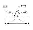
도 11은 도 10에 도시된 특정된 위치에서의 빔의 가우스 강도 프로파일(Gaussian intensity profile)의 개략도이며,
도 12는 본 발명의 일 실시예에 따라 도 10에 도시된 조정된 위치에서의 빔의 가우스 강도 프로파일의 개략도이며,
도 13은 본 발명의 일 실시예에 따라 열적으로 성장된 산화물의 물리적 리프트 오프(lift off) 및 열 응력에 의해 야기된 레이저 제거의 일례의 개략도이며,
도 14는 본 발명의 일 실시예에 따라 플라즈마 강화 화학기상증착(PECVD)에 의해 증착된 실리콘 산화물의 물리적 리프트 오프 및 열 응력에 의해 야기된 레이저 제거의 일례의 개략도이다.1A-1E show schematic cross-sectional views of a solar cell substrate during different stages of the processing sequence used to form a contact structure on the surface of the solar cell,
2 shows a processing sequence used to form a contact structure on a solar cell,
3A is a schematic plan view of an apparatus for executing a processing sequence according to an embodiment of the present invention,
3B is a schematic plan view of an apparatus for executing a processing sequence according to another embodiment of the present invention,
4 is a schematic side view of a robot supporting a substrate over a vision system according to one embodiment of the invention,
5A is a schematic plan view of an apparatus for executing a processing sequence according to another embodiment of the present invention,
5B is a schematic plan view of an apparatus for executing a processing sequence according to another embodiment of the present invention,
6 is a schematic side view of a substrate positioned within a substrate holder in accordance with one embodiment of the present invention;
7A is a schematic plan view of an apparatus for executing a processing sequence according to another embodiment of the present invention,
7B is a schematic plan view of an apparatus for executing a processing sequence according to another embodiment of the present invention,
8 is a schematic plan view of an apparatus for executing a processing sequence according to another embodiment of the present invention,
9 is a schematic plan view of an apparatus for executing a processing sequence according to another embodiment of the present invention,
10 is a schematic diagram of a laser propagating a beam along a distance from the laser,
FIG. 11 is a schematic diagram of a Gaussian intensity profile of a beam at the specified position shown in FIG. 10,
12 is a schematic diagram of a Gaussian intensity profile of a beam at the adjusted position shown in FIG. 10, in accordance with an embodiment of the present invention;
13 is a schematic diagram of an example of laser ablation caused by physical lift off and thermal stress of thermally grown oxide in accordance with one embodiment of the present invention;
14 is a schematic diagram of an example of laser ablation caused by physical lift off and thermal stress of silicon oxide deposited by plasma enhanced chemical vapor deposition (PECVD) in accordance with one embodiment of the present invention.
본 발명의 실시예는 일반적으로 태양 전지의 제조시 사용하는 재료 제거를 위한 방법 및 장치를 제공한다. 일 실시예에서, 패터닝된 유전체 층 위에 전도성 층을 증착하고 희망 패턴에 따라 태양 전지 기판상에 증착되는 유전체 층의 일부를 정밀하게 제거하는 장치가 제공된다. 일 실시예에서, 이 장치는 희망 패턴으로 전도성 층의 일부를 또한 제거한다. 특정 실시예에서, 기저 기판을 손상시키지 않고 레이저에 의해 재료의 일부를 제거하는 방법이 제공된다. 일 실시예에서, 빔의 강도 프로파일은 기판 표면상에 형성된 점(spot) 내에서의 최대 강도와 최소 강도 사이의 차이가 최적 범위로 감소되도록 조정된다. 일례에서, 이 기판은 기판의 둘레(periphery)에 대한 중심의 최고 강도(peak intensity)가 낮아지도록 위치된다. 일 실시예에서, 펄스 에너지(pulse energy)는 유전체 층의 희망 부분의 물리적 리프트-오프(lift-off) 및 열 응력을 제공하도록 개선된다.Embodiments of the present invention generally provide methods and apparatus for material removal for use in the manufacture of solar cells. In one embodiment, an apparatus is provided for depositing a conductive layer over a patterned dielectric layer and precisely removing a portion of the dielectric layer deposited on a solar cell substrate in accordance with a desired pattern. In one embodiment, the device also removes a portion of the conductive layer in the desired pattern. In certain embodiments, a method is provided for removing a portion of a material by a laser without damaging the underlying substrate. In one embodiment, the intensity profile of the beam is adjusted such that the difference between maximum and minimum intensity within a spot formed on the substrate surface is reduced to an optimal range. In one example, the substrate is positioned such that the peak intensity of the center relative to the periphery of the substrate is low. In one embodiment, pulse energy is improved to provide physical lift-off and thermal stress of the desired portion of the dielectric layer.
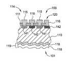
도 1a 내지 도 1e는 태양 전지(100)의 표면상에 접촉 구조물을 형성하는데 사용되는 처리 순서에서 상이한 단계 동안의 태양 전지 기판(110)의 개략적 횡단면도를 도시한다. 도 2는 태양 전지 상에 접촉 구조물을 형성하는데 사용되는 처리 순서(200)를 도시한다.1A-1E show schematic cross-sectional views of the
도 1a를 참조하면, 태양 전지 기판(110)은 전면(101) 및 후면(120)을 갖는다. 일 실시예에서, 기판(110)은 단결정성 실리콘, 멀티 크리스탈 실리콘(multicrystalline silicon), 또는 폴리 크리스탈 실리콘(polycrystalline silicon)을 포함한다. 다른 실시예에서, 기판(110)은 유기 물질, 게르마늄(Ge), 갈륨 비소(GaAs), 카드뮴 텔루라이드(CdTe), 황화 카드뮴(CdS), 구리 인듐 갈륨 셀레나이드(CIGS), 구리 인듐 셀레나이드(CuInSe2), 또는 갈륨 인듐 인화물(GaInP2) 뿐 아니라, ZnSe/GaAs/Ge 또는 GaInP/GaAs/Ge과 같은 이질 접합 셀(heterojunction cells)을 포함할 수 있으며, 이들은 태양광을 전력으로 전환시키는데 사용된다.Referring to FIG. 1A, the
단계(202)에서, 도 1a에 도시된 바와 같이, 유전체 층(111)은 기판(110)의 후면(120) 상에 형성된다. 일 실시예에서, 유전체 층(111)은 실리콘 함유 기판의 표면(120) 상에 형성된 실리콘 이산화물 층과 같은 실리콘 산화물 층이다. 일 실시예에서, 유전체 층(111)은 실리콘 질화물 층, 실리콘 옥시나이트라이드 층, 실리콘 카바이드 층, 실리콘 옥시 카바이드 층, 또는 다른 유사한 유형의 층이다. 유전체 층(111)은 노 어닐링 프로세스(furnace annealing process), 급속 열 산화 프로세스, 대기압 또는 저압 화학 기상 증착(CVD) 프로세스, 플라즈마 강화 CVD 프로세스, 물리 기상 증착(PVD) 프로세스, 증발 프로세스, 분무(spray-on) 프로세스, 스핀-온(spin-on) 프로세스, 롤-온(roll-on) 프로세스, 스크린 인쇄 프로세스, 또는 다른 유사한 증착 프로세스와 같은 통상의 산화 프로세스를 사용하여 형성될 수 있다.In
일 실시예에서, 유전체 층(111)은 두께가 약 50Å 내지 약 3000Å인 실리콘 이산화물 층이다. 다른 실시예에서, 유전체 층(111)은 두께가 약 2000Å 미만인 실리콘 이산화물 층이다. 일 실시예에서, 유전체 층(111)은 약 100Å 내지 약 1000Å의 두께를 갖는 실리콘 질화물 층이다. 다른 실시예에서, 유전체 층(111)은 실리콘 산화물/실리콘 질화물 층 스택, 비정질 실리콘/실리콘 산화물 층 스택, 또는 비정질 실리콘/실리콘 질화물 층 스택과 같은 다층 막 스택을 포함한다. 일 실시예에서, 실리콘 산화물 층은 약 20Å 내지 약 3000Å 두께이며, 실리콘 질화물 층은 약 100Å 내지 약 1000Å 두께이다. 일 실시예에서, 비정질 실리콘 층은 약 30Å 내지 약 100Å 두께이고, 실리콘 산화물 층은 약 100Å 내지 약 3000Å 두께이다. 일 실시예에서, 비정질 실리콘 층은 약 30Å 내지 약 100Å 두께이고, 실리콘 질화물 층은 약 100Å 내지 약 1000Å 두께이다.In one embodiment,
단계(204)에서, 기판(110)의 후면(120)의 영역(125)은 도 1b에 도시된 바와 같이 노출된다. 일 실시예에서, 이 영역(125)은 하나 또는 그보다 많은 레이저 장치(190)를 사용하여 유전체 층(111)의 일부를 제거함으로써 노출된다. 일 실시예에서, 레이저 장치(190)는 Nd:YAG 레이저, Nd:YVO4 레이저 또는 섬유 레이저(fiber laser)와 같은 고체 상태 레이저(solid state laser)이다. 하나 또는 그보다 많은 레이저를 사용하여 유전체 층(111)을 제거하는 방법은 "레이저 제거 방법"이 제목인 섹션에서 추후 설명된다.In
단계(206)에서, 도 1c에 도시된 바와 같이 전도성 층(114)이 기판(110)의 후면(120) 상의 유전체 층(111) 위에 증착된다. 전도성 층(114)은 기판(110)의 후면(120) 상의 노출된 영역(125)을 통해 기판(110)에 전기적으로 연결된다. 일 실시예에서, 형성된 전도성 층(114)은 약 500Å 내지 약 500,000Å의 두께이고, 구리(CU), 은(Ag), 주석(Sn), 코발트(Co), 레늄(Rh), 니켈(Ni), 아연(Zn), 납(Pb) 및/또는 알루미늄(Al)과 같은 금속을 함유한다. 일 실시예에서, 전도성 층(114)은 PVD 프로세스 또는 증발 프로세스에 의해 형성되는 알루미늄(Al) 층이다. 일 실시예에서, 전도성 층(114)은 PVD 프로세스 또는 증발 프로세스에 의해 알루미늄(Al) 층을 먼저 증착한 후, PVD 프로세스에 의해 니켈 바나듐(NiV) 캐핑 층(capping layer)을 증착함으로써 형성되는 2개의 층을 포함한다.In
전도성 층(114)이 서로 맞물린 모든 후면 접촉 태양 전지 구조물 위에 도포되는 실시예에서, 격리된 영역을 형성하도록 증착된 전도성 층(114)을 패터닝하는 것이 바람직할 수 있다. 이러한 실시예에서, 단계(208)는 도 1d에 도시된 바와 같이 실행된다. 일 실시예에서, 기판(110) 내에 형성된 활성 영역에 각각 전기적으로 연결되는 전도성 피처(115, 116)를 형성하도록, 동일하거나 다른 레이저 장치(190)를 사용하여 영역(130) 내의 전도성 층(114)으로부터 재료가 제거된다. 일 실시예에서, 전도성 피처(115)는 기판(110) 내의 p-타입 도핑된 영역(141)과 전기 접촉하고, 전도성 피처(116)는 기판(110) 내에 형성된 n-타입 도핑된 영역(142)과 전기 접촉하며, 이들은 모두 태양 전지(100)의 활성 영역의 일부를 형성한다.In embodiments where the
그 후, 다양한 처리 단계가 실행되어, 도 1e에 도시된 바와 같이 기판의 전면(101)을 준비하고/준비하거나 텍스처링할 수 있다. 일 실시예에서, 전면(101)은 태양 전지가 형성된 후 태양광을 수용하도록 구성된다. 한 경우에, 전면(101)은 텍스처링된 후, 분무 또는 증기상(vapor phase) 고온 확산 프로세스를 사용하여 선택적으로 도핑된다. 전면(101)은 그 후 반사 방지(ARC) 층(119)(예를 들면, 실리콘 질화물)을 증착함으로써 부동화된다(passivated). 일 실시예에서, 하나 또는 그보다 많은 활성 층(118)(예를 들면, p-타입 기판 상의 i-n 타입 층)을 갖는 이질 접합형 태양 전지는 텍스처링된 전면(101) 상에 형성된다. 일 실시예에서, 전면의 준비는 프로세스 순서(200)를 실행하기 전에 실행된다. 일 실시예에서, 전면(101)을 준비한 후, 태양 전지(100)의 전방 접촉 구조물을 형성하도록 통상의 프로세스를 사용하여 전면 상에 하나 또는 그보다 많은 전도성 전방 접촉 라인(미도시)이 형성될 수 있다.Various processing steps may then be performed to prepare and / or texturize the
일 실시예에서, 기판(110)의 전면(101) 상에 배치된 하나 또는 그보다 많은 층의 일부는 (전술된) 레이저 장치(190)와 같은 하나 또는 그보다 많은 레이저 장치를 사용하여 제거된다. 부동화 및/또는 ARC 층을 제거하는 방법은 제목이 "레이저 제거 방법"인 섹션에서 추후 설명된다. 일례에서, 하나 또는 그보다 많은 전도성 전방 접촉 라인(또는 핑거)이 그 후 레이저 제거 프로세스에 의해 노출된 영역 위에 증착된다. 하나 또는 그보다 많은 전도성 전방 접촉 라인은 그 후 더 처리될 수 있어서, 바람직한 전기 연결이 기판(110)의 전면(101) 상의 노출된 영역을 통해 기판(110) 상에 형성되는 것을 보장한다. 일 실시예에서, 하나 또는 그보다 많은 전도성 전방 접촉 라인은 구리(Cu), 은(Ag), 주석(Sn), 코발트(Co), 레늄(Rh), 니켈(Ni), 아연(Zn), 납(Pb) 및/또는 알루미늄(Al)과 같은 금속을 함유한다.In one embodiment, some of the one or more layers disposed on the
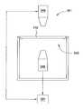
도 3a는 본 발명의 일 실시예에 따른 단계(204 내지 208)를 실행하는 장치(300A)의 개략적 평면도이다. 도 3b는 본 발명의 다른 실시예에 따른 단계(204 내지 208)를 실행하는 장치(300B)의 개략적 평면도이다. 일 실시예에서, 자신의 후면(120) 상에 증착된 유전체 층(111)을 갖는 기판(110)은 유입 컨베이어(310)에 의해 수용 영역(320)으로 이송된다. 일 실시예에서, 기판(110)은 유입 컨베이어(310) 상으로 개별적으로 이송된다. 다른 실시예에서, 기판(110)은 카세트로 이송된다. 다른 실시예에서, 기판(110)은 스택 박스(stack boxes)로 이송된다. 일 실시예에서, 각각의 개별적인 기판(110)이 수용 영역(320)으로 전달되면, 이송 로봇(330)이 수용 영역(320)으로부터 각각의 기판(110)을 회수하고, 비전 시스템(340) 위에서 기판(110)을 지지한다.3A is a schematic top view of an
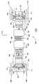
도 4는 비전 시스템(340) 위에서 기판(110)을 지지하는 로봇(330)의 개략적 측면도이다. 일 실시예에서, 비전 시스템(340)은 상부를 보는 검사 장치(342), 조명 소오스(344) 및 레이저 스캐너(346)를 포함한다. 일 실시예에서, 검사 장치(342)는 컬러 카메라 또는 흑백 카메라와 같은 카메라이다. 일 실시예에서, 조명 소오스(344)는 특정된 파장 범위 내에서 빛을 방출하도록 구성된 발광 다이오드(LED) 소오스이다. 다른 실시예에서, 조명 소오스(344)는 기판(110)을 향해 원하는 빛의 파장을 방출하기 위해, 하나 또는 그보다 많은 필터(미도시) 및 광대역 램프를 포함한다. 일 실시예에서, 레이저 스캐너(346)는 전술된 레이저 장치(190)와 같은 고체 상태 레이저를 포함한다. 일 실시예에서, 검사 장치(342), 조명 소오스(344), 및 레이저 스캐너(346)는 시스템 제어기(301)와 통신한다.4 is a schematic side view of the
시스템 제어기(301)는 전체 장치(300A 또는 300B)의 자동화 및 제어를 용이하게 하며, 중앙 처리 유닛(CPU)(미도시), 메모리(미도시), 및 지원 회로(또는 I/O)(미도시)를 포함할 수 있다. CPU는 다양한 챔버 프로세스 및 하드웨어(예를 들면, 컨베이어, 광학 검사 조립체, 모터, 유체 전달 하드웨어 등)를 제어하기 위한 산업 설정에 사용되고 시스템 및 챔버 프로세스(예를 들면, 기판 위치, 프로세스 시간, 탐지기 신호 등)를 모니터링하는 임의의 형태의 컴퓨터 프로세서 중 하나일 수 있다. 메모리는 CPU에 연결되며, 임의 접근 메모리(RAM), 판독 전용 메모리(ROM), 플로피 디스크, 하드 디스크, 또는 임의의 다른 형태의 디지털 로컬 또는 원격 저장소와 같이 용이하게 이용 가능한 메모리 중 하나 이상일 수 있다. 소프트웨어 명령 및 데이터는 CPU에 명령하기 위해 메모리 내에 코드화되어 저장될 수 있다. 지원 회로는 또한 통상의 방식으로 프로세스를 지원하기 위해 CPU에 연결된다. 지원 회로는 캐시(cache), 전원, 시간 기록 회로(clock circuits), 입력/출력 회로, 하부 시스템 등을 포함할 수 있다. 시스템 제어기(301)에 의해 판독 가능한 프로그램(또는 컴퓨터 명령)은 기판상에서 어떠한 작업이 실행가능한지를 결정한다. 바람직하게, 이 프로그램은 시스템 제어기(301)에 의해 판독 가능한 소프트웨어이며, 적어도 기판 위치상의 정보, 다양한 제어 구성요소들의 이동 순서, 기판의 광학적 검사 시스템 정보 및 이들의 임의의 조합을 발생시키고 저장하도록 하는 코드를 포함한다.
일 실시예에서, 로봇(330)이 비전 시스템(340) 위에서 기판(110)을 지지할 때, 검사 장치(342) 및 조명 소오스(344)는 시스템 제어기(301)와 함께 작동하여, 레이저 스캐너(346)에 대한 기판(110)이 정밀한 위치를 결정한다. 이러한 측정은 그 후 레이저 패터닝을 위해 레이저 스캐너(346)에 대해 기판(110)을 정밀하게 정렬시키는데 사용된다. 일 실시예에서 이러한 측정은 그 후 레이저 패터닝을 위해 기판(110)에 대해 레이저 스캐너(346)를 정밀하게 정렬시키는데 사용된다. 레이저 스캐너(346)는 그 후 전술된 단계(204)에 따라 희망 패턴으로 유전체 층(111)의 일부를 제거한다. 패터닝 후, 패터닝된 기판(110)의 표면은 추가 처리 이전에 검사 장치(342)에 의해 검사될 수 있다.In one embodiment, when the
다른 실시예에서, 비전 시스템(340)은 수용 영역(320) 내에 위치된다. 이 실시예에서, 조명 소오스(344)는 기판(110)의 일측면 상에 위치될 수 있고, 검사 장치(342)는 기판(110)의 반대 측면 상에 위치될 수 있다. 예를 들면, 검사 장치(342)는 기판(110) 위에 놓일 수 있지만, 조명 소오스(344)는 기판(110) 아래에 놓인다. 이 실시예에서, 검사 장치(342)가 기판(110)의 이미지를 획득(capture)하고 이 이미지를 시스템 제어기(301)로 전달하는 동안, 조명 소오스(344)는 후방 조명(back lighting)을 제공할 수 있다.In another embodiment,
다시 도 3을 참조하면, 로봇(330)은 그 후 패터닝된 기판(110)을 기판 이송 표면(350) 상의 특정 피처(352) 안에 배치한다. 일 실시예에서, 이 피처(352)는 포켓(pockets)이며, 기판 이송 표면(350)은 기판 캐리어이다. 다른 실시예에서, 피처(352)는 지지 요소이며, 기판 이송 표면(350)은 기판 핸들링 로봇 상의 복수의 측면 아암을 포함한다. 다른 실시예에서, 피처(352)는 지지 요소 또는 포켓이며, 기판 이송 표면(350)은 기판 컨베이어의 상부 표면과 같은 자동화 시스템(381)의 플랫폼 부분이다. 기판 이송 표면(350)의 피처(352) 각각이 패터닝된 기판(110)으로 채워진 후, 기판(110)은 자동화 시스템(381)에 의해 증발 챔버 또는 PVD 챔버와 같은 증착 챔버(360)로 이송된다. 일 실시예에서, 자동화 시스템(381)은 기판 이송 표면(350) 상에서 기판(110)을 선형적으로 이동시키기 위한 액츄에이터(미도시) 및 롤러(미도시)를 포함한다. 일 실시예에서, 자동화 시스템(381)은 기판 핸들링 로봇이다. 증착 챔버(360)에서, 전도성 층(114)은 전술된 단계(206)에 따라 패터닝된 유전체 층(111) 위에 증착된다.Referring again to FIG. 3, the
일 실시예에서, 전도성 층(114)이 증착된 후, 기판(110)은 자동화 시스템(381)에 의해 증착 챔버(360)로부터 기판 이송 표면(350) 상으로 이송된다. 이때, 동일하거나 다른 로봇(330)이 그 각각의 피처(352)로부터 개별적인 기판(110)을 제거하고 이를 동일하거나 다른 비전 시스템(340) 위에서 지지할 수 있다. 일 실시예에서, 기판(110)의 정밀한 위치 결정은 시스템 제어기(301)와 와 함께 조명 소오스(344) 및 검사 장치(342)에 의해 다시 결정된다. 이러한 측정은 그 후 전술된 단계(208)에 따른 전도성 층(114)의 레이저 패터닝을 위해, 기판(110)에 대해 레이저 스캐너(346)를 정밀하게 정렬시키거나 레이저 스캐너(346)에 대해 기판(110)을 정밀하게 정렬시키는데 사용될 수 있다. 일 실시예에서, 패터닝된 전도성 층(114)은 그 후 비전 시스템(340)에 의해 검사될 수 있다. 로봇(330)은 그 후 기판(110)을 출구 영역(370)에 배치하며, 이들을 배출 컨베이어(380) 상에서 장치(300A 또는 300B)로부터 멀리 이송되게 할 수 있다.In one embodiment, after the
도 3a 및 도 3b에 도시된 실시예는 각각의 개별적인 기판(110)이 레이저 스캐너(346)의 좌표계에 대해 위치되기 때문에, 기판(110)의 층 상에 레이저 패턴을 대단히 정밀하게 위치시키도록 제공된다. 이 실시예는 또한 비교적 단순한 레이저 헤드(laser head) 설계를 허용하는데, 이는 레이저 작동 영역이 단일한 기판(110)의 크기로 제한되기 때문이다. 추가로, 기판 파손의 가능성이 최소화되는데, 이는 각각의 기판이 일단 사전 증착 측에 있고, 증착 챔버(360)의 사후 증착 측에 있으면, 단지 로봇(340)에 의해서 이동되기 때문이다.3A and 3B provide for highly precise positioning of the laser pattern on the layer of
도 5a는 본 발명의 다른 실시예에 따라 단계(204 내지 208)를 실행하는 장치(500A)의 개략적 평면도이다. 도 5b는 본 발명의 다른 실시예에 따라 단계(204 내지 208)를 실행하는 장치(500B)의 개략적 평면도이다. 일 실시예에서, 자신의 후면(120) 상에 증착되는 유전체 층(111)을 갖는 기판(110)은 유입 컨베이어(510)에 의해 수용 영역(520)으로 이송된다. 일 실시예에서, 기판(110)은 유입 컨베이어(510)로 개별적으로 이송된다. 다른 실시예에서, 기판(110)은 카세트로 이송된다. 다른 실시예에서, 기판(110)은 스택 박스로 이송된다.5A is a schematic top view of an
일 실시예에서, 비전 시스템(540)은 수용 영역(520) 내에 위치된다. 이 실시예에서, 조명 소오스(544)는 기판(110)의 일 측면 상에 위치될 수 있고, 검사 장치(542)는 기판(110)의 반대 측면 상에 위치될 수 있다. 예를 들면, 검사 장치(542)는 기판(110) 위에 위치될 수 있지만, 조명 소오스(544)는 기판(110) 아래에 위치된다. 이 실시예에서, 검사 장치(542)가 기판(110)의 이미지를 획득하고 이 이미지를 시스템 제어기(301)로 전달하는 동안, 조명 소오스(544)는 후방 조명을 제공할 수 있다. 일 실시예에서, 검사 장치(542) 및 조명 소오스(544)는 시스템 제어기(301)와 함께 작동하여 기판(110)의 정밀한 위치를 결정한다.In one embodiment,
일 실시예에서, 각각의 개별적인 기판(110)이 수용 영역(520)으로 전달되면, 이송 로봇(530)이 수용 영역(520)으로부터 기판(110)을 회수하고, 기판(110)의 위치에 관한 정보를 사용하여, 기판 홀더(541) 상에 기판(110)을 배치한다. 도 6은 기판 홀더(541) 내에 위치되는 기판(110)의 개략적인 측면도이다. 이 실시예에서, 기판 홀더(541)는 기판 포켓(548) 및 이 기판 포켓(548) 아래에 위치되는 레이저 스캐너(546)를 포함하며, 이 경우, 유전체 층(111)은 아래를 향하는 기판(110)의 측면상에 제공된다. 위를 향하는 기판(110)의 측면상에 유전체 층(111)이 제공되는 실시예에서, 레이저 스캐너(546)가 기판 포켓(548) 위에 위치된다. 일 실시예에서, 레이저 스캐너(546)는 레이저 장치(190)와 같은 고체 상태 레이저를 포함한다. 일 실시예에서, 레이저 스캐너(546)는 그 후 전술된 단계(204)에 따라 희망 패턴으로 유전체 층(111)의 일부를 제거한다. 일 실시예에서, 하나의 기판(110)은 기판 홀더(541)의 하나의 기판 포켓(548) 내에서 패터닝되는 반면, (이미 패터닝된) 다른 기판(110)은 인접한 기판 포켓(548)으로부터 제거될 수 있고/있거나, 제3 기판(110)이 인접한 기판 포켓(548) 상에 로딩될 수 있다. 일 실시예에서, 기판 홀더(541)는 기판(110)의 패터닝된 표면을 검사하기 위해 조명 소오스(544) 및 검사 장치(542)를 더 포함할 수 있다.In one embodiment, once each
다시 도 5a 및 도 5b를 참조하면, 로봇(530)은 그 후 기판 이송 표면(550) 상의 특정 피처(552) 안에 패터닝된 기판(110)을 배치한다. 일 실시예에서, 이 피처(552)는 포켓이며, 기판 이송 표면(550)은 기판 캐리어이다. 다른 실시예에서, 피처(552)는 지지 요소이고, 기판 이송 표면(550)은 기판 핸들링 로봇 상의 복수의 측면 아암을 포함한다. 다른 실시예에서, 피처(552)는 지지 요소 또는 포켓이고, 기판 이송 표면(550)은 기판 컨베이어의 상부 표면과 같은 자동화 시스템(581)의 플랫폼 부분이다. 기판 이송 표면(550)의 피처(552) 각각이 패터닝된 기판(110)으로 채워진 후, 기판(110)은 자동화 시스템(581)에 의해 증발 챔버 또는 PVD 챔버와 같은 증착 챔버(560)로 이송된다. 일 실시예에서, 자동화 시스템(581)은 기판 이송 표면(550) 상에서 기판(110)을 선형적으로 이동시키기 위해 액츄에이터(미도시) 및 롤러(미도시)를 포함한다. 일 실시예에서, 자동화 시스템(581)은 기판 핸들링 로봇이다. 전도성 층(114)은 그 후 전술된 단계(206)에 따라 패터닝된 유전체 층(111) 위에 증착된다.Referring again to FIGS. 5A and 5B, the
일 실시예에서, 전도성 층(114)이 증착된 후, 기판(110)은 증착 챔버(560)의 외부로 이송된다. 이때, 동일하거나 다른 로봇(530)은 그 각각의 피처(552)로부터 개별적인 기판(110)을 제거하고 이를 동일하거나 다른 기판 홀더(541) 내에 배치할 수 있다. 레이저 스캐너(546)는 그 후 전술된 단계(208)에 따라 전도성 층(114)을 레이저 패터닝할 수 있다. 일 실시예에서, 검사 장치(542) 및 조명 소오스(544)는 패터닝된 전도성 층(114)을 검사하는데 사용될 수 있다. 일 실시예에서, 로봇(530)은 그 후 기판(110)을 출구 영역(570)에 배치하며, 이들을 배출 컨베이어(580) 상에서 장치(500A 또는 500B)로부터 멀리 이송되게 할 수 있다.In one embodiment, after the
도 5a 및 도 5b에 도시된 실시예는 각각의 개별적인 기판(110)이 레이저 스캐너(546)의 좌표계에 대해 위치되기 때문에, 기판(110)의 층 상에 레이저 패턴을 대단히 정밀하게 위치시키도록 제공된다. 이 실시예는 또한 비교적 단순한 레이저 헤드 설계를 허용하는데, 이는 레이저 작동 영역이 2개의 기판(110)의 크기로 제한되기 때문이다. 추가로, 장치(500A 또는 500B)의 증가된 기판(110) 수율이 획득될 수 있는데, 이는 인접한 기판(110)이 레이저 패터닝되는 동안 로봇(530)이 하나의 기판(110)을 로딩/언로딩할 수 있기 때문이다.5A and 5B provide for highly precise positioning of the laser pattern on the layer of
도 7a는 본 발명의 일 실시예에 따라 단계(204 내지 208)를 실행하는 장치(700A)의 개략적 평면도이다. 도 7b는 본 발명의 다른 실시예에 따라 단계(204 내지 208)를 실행하는 장치(700B)의 개략적 평면도이다. 일 실시예에서, 자신의 후면(120) 상에 증착된 유전체 층(111)을 갖는 기판(110)은 유입 컨베이어(710)에 의해 수용 영역(720)으로 이송된다. 일 실시예에서, 기판(110)은 유입 컨베이어(710) 상으로 개별적으로 이송된다. 다른 실시예에서, 기판(110)은 카세트로 이송된다. 다른 실시예에서, 기판(110)은 스택 박스로 이송된다. 일 실시예에서, 비전 시스템(740)은 수용 영역(720) 내에 위치된다. 이 실시예에서, 조명 소오스(744)는 기판(110)의 일 측면상에 위치될 수 있고, 검사 장치(742)는 기판(110)의 반대 측면상에 위치될 수 있다. 예를 들면, 검사 장치(742)는 기판(110) 위에 위치될 수 있는 반면, 조명 소오스(744)는 기판(110) 아래에 위치된다. 이 실시예에서, 검사 장치(742)가 기판(110)의 이미지를 획득하고 이 이미지를 시스템 제어기(301)로 전달하는 동안, 조명 소오스(744)는 후방 조명을 제공하여, 예상 위치에 대하여 기판(110)의 정밀한 위치를 결정할 수 있다.7A is a schematic top view of an
다른 실시예에서, 각각의 개별적인 기판(110)이 수용 영역(720)으로 전달되면, 이송 로봇(730)이 수용 영역(720)으로부터 기판(110)을 회수하고, 비전 시스템(740) 위에서 기판(110)을 지지한다. 일 실시예에서, 로봇(730)이 비전 시스템(740) 위에서 기판(110)을 지지할 때, 비전 시스템(740)은 시스템 제어기(301)와 함께 작동하여, 예상 위치에 대하여 기판(110)의 정밀한 위치를 결정한다.In another embodiment, when each
다음으로, 이러한 측정은 기판 이송 표면(750) 상의 특정 피처(752) 내에 기판(110)을 정밀하게 위치시키는데 사용될 수 있다. 일 실시예에서, 이 피처(752)는 포켓이며, 기판 이송 표면(750)은 기판 캐리어이다. 다른 실시예에서, 피처(752)는 지지 요소이며, 기판 이송 표면(750)은 기판 핸들링 로봇 상의 복수의 측면 아암을 포함한다. 다른 실시예에서, 피처(752)는 지지 요소 또는 포켓이며, 기판 이송 표면(750)은 기판 컨베이어의 상부 표면과 같은 자동화 시스템(781)의 플랫폼 부분이다. 일 실시예에서, 자동화 시스템(781)은 기판 이송 표면(750) 상에서 기판(110)을 선형적으로 이동시키기 위해 액츄에이터(미도시) 및 롤러(미도시)를 포함한다. 일 실시예에서, 자동화 시스템(781)은 기판 핸들링 로봇이다.This measurement can then be used to precisely position the
기판 이송 표면(750)의 피처(752) 각각이 패터닝된 기판(110)으로 채워진 후, 기판(110)은 전술된 단계(204)에 따라서 및 희망 패턴에 따라서 기판 이송 표면(750) 상에 위치된 각각의 기판(110)의 유전체 층(111)의 일부를 제거하기 위해, 레이저 스캐너(746) 아래로(위를 향하는 기판(110)의 측면 상에 유전체 층(111)이 제공되는 실시예에서) 또는 레이저 스캐너 위로(아래를 향하는 기판(110)의 측면상에 유전체 층(111)이 제공되는 실시예에서) 자동화 시스템(781)에 의해 이송된다. 일 실시예에서, 레이저 스캐너(746)는 레이저 장치(190)와 같은 고체 상태 레이저를 포함한다. 일 실시예에서, 레이저 스캐너(746)는 Y 방향으로 이동하도록 구성된다. 이러한 실시예에서, 기판(110)은 각각의 열에서 각각의 기판(110)을 패터닝하기 위해 한번에 한열 씩, 자동화 시스템(781)에 의해 레이저 스캐너(746)를 지나서 인덱스된다(indexed). 다른 실시예에서, 레이저 스캐너(746)는 X 방향 및 Y 방향으로 이동하도록 구성된다.After each of the
일 실시예에서, 장치(700A 또는 700B)는 레이저 스캐너(746)에 대해 기판 이송 표면(750)의 정밀한 위치설정을 결정하기 위해 비전 시스템(790)을 포함한다. 일 실시예에서, 기판 이송 표면(750)의 정확한 위치는 기판 이송 표면(750) 상에 형성된 하나 또는 그보다 많은 기준 마크(fiducial marks) 및 비전 시스템(790)을 사용하여 결정된다. 비전 시스템(790)은 기판 이송 표면(750) 상에서 발견되는 기준 마크를 조사하도록 위치되는 탐지기를 포함한다. 레이저 스캐너(746)의 알려진 위치에 대한 기판 이송 표면(750)의 각도 배향 및 위치는 그 후 시스템 제어기(301)에 의해 결정될 수 있다. 이러한 오프셋(offset)은 그 후 각각의 기판(110)의 유전체 층(111)을 패터닝하기 위해 레이저 스캐너(746)를 정밀하게 위치시키는데 사용될 수 있다. 또한, 비전 시스템(790)은 각각의 기판(110)의 패터닝된 유전체 층(111)을 검사하는데 사용될 수 있다.In one embodiment, the
일 실시예에서, 각각의 기판(110)의 유전체 층(111)을 패터닝한 후에, 기판은 자동화 시스템(781)에 의해 증발 챔버 또는 PVD 챔버와 같은 증착 챔버(760)로 이송된다. 증착 챔버(760)에서, 전도성 층(114)은 전술된 단계(206)에 따라 각각의 기판(110)의 패터닝된 유전체 층(111) 위에 증착된다.In one embodiment, after patterning the
일 실시예에서, 전도성 층(114)이 각각의 기판(110) 위에 증착된 후, 기판(110)은 자동화 시스템(781)에 의해 증착 챔버(760)의 외부로 이송된다. 일 실시예에서, 다른 레이저 스캐너(746)는 그 후 전술된 단계(208)에 따라 각각의 기판(110)의 전도성 층(114)을 패터닝한다.In one embodiment, after the
이때, 동일하거나 다른 로봇(730)이 그 각각의 피처(752)로부터 각각의 기판(110)을 제거하고, 이 기판(110)을 출구 영역(770)에 배치할 수 있으며, 이들을 배출 컨베이어(780) 상에서 장치(700A 또는 700B)로부터 멀리 이송되게 할 수 있다.At this time, the same or
도 7a 및 도 7b에 도시된 실시예는 각각의 개별적인 기판(110)이 레이저 스캐너(746)의 좌표계에 대해 위치될 수 있고/있거나 각각의 기판 이송 표면(750)이 레이저 스캐너(746)의 좌표계에 대해 위치될 수 있기 때문에, 기판(110)의 층 상에 레이저 패턴을 대단히 정밀하게 위치시키도록 제공된다. 추가로, 도 7a 및 도 7b의 실시예는 이송 로봇(730)의 기판 수율에 영향을 미치지 않는데, 이는 모든 패터닝 프로세스가 기판(110)의 로딩 이후 및/또는 언로딩 이전에 실행되기 때문이다.7A and 7B show that each
도 8은 본 발명의 일 실시예에 따른 단계(202 내지 208)를 실행하는 장치(800)의 개략적 평면도이다. 일 실시예에서, 기판(110)은 유입 컨베이어(810)에 의해 수용 영역(820)으로 이송된다. 일 실시예에서, 기판(110)은 유입 컨베이어(810) 상으로 개별적으로 이송된다. 다른 실시예에서, 기판(110)은 카세트로 이송된다. 다른 실시예에서, 기판(110)은 스택 박스로 이송된다. 일 실시예에서, 비전 시스템(840)은 수용 영역(820) 내에 위치된다. 이 실시예에서, 조명 소오스(844)는 기판(110)의 일 측면상에 위치될 수 있고, 검사 장치(842)는 기판(110)의 반대 측면상에 위치될 수 있다. 예를 들면, 검사 장치(842)는 기판(110) 위에 위치될 수 있지만, 조명 소오스(844)는 기판(110) 아래에 위치된다. 이 실시예에서, 검사 장치(842)가 기판(110)의 이미지를 획득하고 이 이미지를 시스템 제어기(301)로 전달하는 동안, 조명 소오스(844)는 후방 조명을 제공하여, 예상 위치에 대해 기판(110)의 정밀한 위치를 결정할 수 있다.8 is a schematic top view of an
다음으로, 이러한 측정은 기판 이송 표면(850) 상의 특정 피처(852) 내에 기판(110)을 정밀하게 위치시키는데 사용될 수 있다. 일 실시예에서, 이 피처(852)는 포켓이며, 기판 이송 표면(850)은 기판 캐리어이다. 다른 실시예에서, 피처(852)는 지지 요소 또는 포켓이며, 기판 이송 표면(850)은 기판 컨베이어의 상부 표면과 같은 자동화 시스템(881)의 플랫폼 부분이다.This measurement can then be used to precisely position the
기판 이송 표면(850)의 피처(852) 각각이 패터닝된 기판(110)으로 채워진 후, 기판(110)은 자동화 시스템(881)에 의해 PVD 챔버 또는 CVD 챔버와 같은 증착 챔버(855)로 이송된다. 일 실시예에서, 자동화 시스템(881)은 기판 이송 표면(850) 상에서 기판(110)을 선형적으로 이동시키기 위해 액츄에이터(미도시) 및 롤러(미도시)를 포함한다. 증착 챔버(855)에서, 유전체 층(111)은 각각의 기판(110)의 후면(120) 상에 증착된다.After each of the
유전체 층(111)이 증착된 후, 기판은 전술된 단계(204)에 따라서 및 희망 패턴에 따라 기판 이송 표면(850) 상에 위치된 기판 각각의 유전체 층(111)의 일부를 제거하기 위해 레이저 스캐너(846)로 이송된다. 일 실시예에서, 레이저 스캐너(846)는 레이저 장치(190)와 같은 고체 상태 레이저를 포함한다. 일 실시예에서, 레이저 스캐너(846)는 Y방향으로 이동하도록 구성된다. 이러한 실시예에서, 기판(110)은 각각의 열에서 각각의 기판(110)을 패터닝하기 위해, 한번에 한열 씩, 자동화 시스템(881)에 의해 레이저 스캐너(846)를 지나서 인덱스된다. 다른 실시예에서, 레이저 스캐너(846)는 X 방향 및 Y 방향으로 이동하도록 구성된다.After the
일 실시예에서, 장치(800)는 레이저 스캐너(846)에 대해 기판 이송 표면(850)의 정밀한 위치 설정을 결정하기 위한 비전 시스템(890)을 포함한다. 일 실시예에서, 기판 이송 표면(850)의 정확한 위치는 기판 이송 표면(850) 상에 형성된 하나 또는 그보다 많은 기준 마크 및 비전 시스템(890)을 사용하여 결정된다. 이 비전 시스템(890)은 기판 이송 표면(850) 상에서 발견되는 기준 마크를 조사하도록 위치되는 탐지기를 포함한다. 레이저 스캐너(846)의 알려진 위치에 대한 기판 이송 표면(850)의 각도 배향 및 위치는 그 후 시스템 제어기(301)에 의해 결정될 수 있다. 이러한 오프셋은 그 후 각각의 기판(110)의 유전체 층(111)을 패터닝하기 위해 레이저 스캐너(846)를 정밀하게 위치시키는데 사용될 수 있다. 또한, 비전 시스템(890)은 각각의 기판(110)의 패터닝된 유전체 층(111)을 검사하는데 사용될 수 있다.In one embodiment, the
일 실시예에서, 각각의 기판(110)의 유전체 층(111)을 패터닝한 후에, 기판(110)은 자동화 시스템(881)에 의해 증발 챔버 또는 PVD 챔버와 같은 증착 챔버(860)로 이송된다. 증착 챔버(860)에서, 전도성 층(114)은 전술된 단계(206)에 따라 각각의 기판(110)의 패터닝된 유전체 층(111) 위에 위치된다.In one embodiment, after patterning the
일 실시예에서, 전도성 층(114)이 각각의 기판(110) 상에 증착된 후, 기판(110)은 자동화 시스템(881)에 의해 증착 챔버(860)의 외부로 이송된다. 일 실시예에서, 다른 레이저 스캐너(846)는 그 후 전술된 단계(208)에 따라 각각의 기판(110)의 전도성 층(114)을 패터닝한다.In one embodiment, after the
이때, 다른 로봇(830)은 그 각각의 피처(852)로부터 각각의 기판(110)을 제거하고, 이 기판(110)을 출구 영역(870)에 배치할 수 있으며, 이들을 배출 컨베이어(880) 상에서 장치(800)로부터 멀리 이송되게 할 수 있다.At this time, the
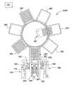
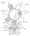
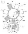
도 9는 본 발명의 일 실시예에 따라 단계(202 내지 208)를 실행하는 장치(900)의 개략적 평면도이다. 일 실시예에서, 기판(110)은 유입 컨베이어(910)에 의해 수용 영역(920)으로 이송된다. 일 실시예에서, 기판(110)은 유입 컨베이어(910) 상으로 개별적으로 이송된다. 다른 실시예에서, 기판(110)은 카세트로 이송된다. 다른 실시예에서, 기판(110)은 스택 박스로 이송된다. 일 실시예에서, 비전 시스템(940)은 수용 영역(920) 내에 위치된다. 이 실시예에서, 조명 소오스(944)는 기판(110)의 일측면 상에 위치될 수 있고, 검사 장치(942)는 기판(110)의 반대 측면상에 위치될 수 있다. 예를 들면, 검사 장치(942)는 기판(110) 위에 위치될 수 있는 반면, 조명 소오스(944)는 기판(110) 아래에 놓인다. 이 실시예에서, 검사 장치(942)가 기판(110)의 이미지를 획득하고 이 이미지를 시스템 제어기(301)로 전달하는 동안, 조명 소오스(944)는 후방 조명을 제공하여, 예상 위치에 대해 기판(110)의 정밀한 위치를 결정할 수 있다.9 is a schematic plan view of an
다음으로, 이러한 측정은 기판 이송 표면(950) 상의 특정 피처(952)로 기판(110)을 정밀하게 위치시키는데 사용될 수 있다. 일 실시예에서, 피처(952)는 포켓이며, 기판 이송 표면(950)은 기판 캐리어이다. 다른 실시예에서, 피처(952)는 지지 요소이고, 기판 이송 표면(950)은 기판 핸들링 로봇 상의 복수의 측면 아암을 포함한다.This measurement can then be used to precisely position the
기판 이송 표면(950)의 피처(952) 각각이 기판(110)으로 채워진 후, 기판(110)은 자동화 시스템(981)에 의해 로드록 챔버(953)로 이송된다. 일 실시예에서, 자동화 시스템(981)은 기판 핸들링 로봇이다. 다음으로, 일 실시예에서, 로드록 챔버(953)는 진공 펌프(미도시)를 사용하여 희망 압력으로 펌프 다운(pumped down)된다. 로드록 챔버(953) 내에 희망 압력을 획득한 후, 기판(110)은 자동화 시스템(981)에 의해 CVD 또는 PVD 챔버와 같은 증착 챔버(955)로 이송된다. 일 실시예에서, 자동화 시스템은 추가의 기판 핸들링 로봇을 포함한다. 증착 챔버(955)에서, 유전체 층(111)은 전술된 단계(202)에 따라 각각의 기판(110)의 후면(120) 상에 증착된다.After each of the
유전체 층(111)이 증착된 후, 기판(110)은 전술된 단계(204)에 따라서 및 희망 패턴에 따라 기판 이송 표면(950) 상에 위치된 기판 각각의 유전체 층(111)의 일부를 제거하기 위해 레이저 스캐너(946)로 이송된다. 일 실시예에서, 레이저 스캐너(946)는 레이저 장치(190)와 같은 고체 상태 레이저를 포함한다.After the
일 실시예에서, 장치(900)는 레이저 스캐너(946)에 대해 기판 이송 표면(950)의 정밀한 위치 설정을 결정하기 위한 비전 시스템(990)을 포함한다. 일 실시예에서, 기판 이송 표면(950)의 정확한 위치는 기판 이송 표면(950) 상에 형성된 하나 또는 그보다 많은 기준 마크 및 비전 시스템(9900)을 사용하여 결정된다. 비전 시스템(990)은 기판 이송 표면(950) 상에서 발견되는 기준 마크를 조사하도록 위치되는 탐지기를 포함한다. 레이저 스캐너(946)의 알려진 위치에 대한 기판 이송 표면(950)의 각도 배향 및 위치는 그 후 시스템 제어기(301)에 의해 결정될 수 있다. 이러한 오프셋은 그 후 각각의 기판(110)의 유전체 층(111)을 패터닝하기 위해 레이저 스캐너(946)를 정밀하게 위치시키도록 사용될 수 있다. 또한, 비전 시스템(990)은 각각의 기판(110)의 패터닝된 유전체 층(111)을 검사하는데 사용될 수 있다.In one embodiment, the
일 실시예에서, 각각의 기판(110)의 유전체 층(111)을 패터닝한 후, 기판(110)은 자동화 시스템(981)에 의해 증발 챔버 또는 PVD 챔버와 같은 증착 챔버(960)로 이송된다. 증착 챔버(960)에서, 전도성 층(114)은 전술된 단계(206)에 따라 각각의 기판(110)의 패터닝된 유전체 층(111) 위에 증착된다.In one embodiment, after patterning the
일 실시예에서, 전도성 층(114)이 각각의 기판(110) 상에 증착된 후, 기판(110)은 전술된 단계(208)에 따라 전도성 층(114)을 패터닝하기 위해 동일하거나 상이한 레이저 스캐너(946)로 이송된다. 일 실시예에서, 비전 시스템(990)은 각각의 기판(110)의 패터닝된 전도성 층(114)을 검사하는데 사용될 수 있다.In one embodiment, after
일 실시예에서, 기판(110)은 그 후 로드록 챔버(953)로 다시 이동된 후 로드록 챔버(953)의 외부로 이송된다. 이때, 동일하거나 다른 로봇(930)은 그 각각의 피처(952)로부터 각각의 기판(110)을 제거하고, 이 기판(110)을 출구 영역(970)에 배치할 수 있으며, 이들을 배출 컨베이어(980) 상에서 장치(900)로부터 멀리 이송되게 할 수 있다.
In one embodiment, the
레이저 제거 방법Laser Removal Method
상기 제시된 바와 같이, 재료 층의 일부(예를 들면, 유전체 층(111) 또는 전도성 층(114))를 제거하는 것은 레이저 장치(190)의 사용에 의해 이루어질 수 있다. 통상적으로, 재료 제거는 재료 층의 완전한 증발을 얻기 위해, 기판(110) 상의 특정 점(specific spot)에서의 감응, 펄스 기간, 파장, 및 특정한 주파수에서 레이저 장치(190)를 펄싱함으로써 실행된다. 그러나 기저 기판(110)을 손상시키지 않고 재료 층, 특히 유전체 층(111)의 일부의 완전한 증발을 얻기는 어렵다.As set forth above, removing a portion of the material layer (eg,
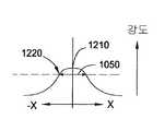
기판(110)을 손상시키지 않고 유전체 층(111)의 일부를 제거하는 어려움의 한가지 이유는 기판(110) 상에 집중되는 레이저 점(laser spot)의 영역에 걸친 강도의 변화에 의한 것이다. 순수한 가우스 프로파일을 갖는(즉, 기본 가로축 모드(fundamental transverse mode) 또는 TEM00 모드 상에서 작동하는) 빔을 방출하는 이상적인 레이저에서, 제거될 재료상의 희망 점의 중심에서의 최고 강도는 이 점의 둘레 주위에서보다 더 높다. 도 10은 레이저 장치(190)로부터 거리(Z)를 따라 빔(1000)을 전파하는 레이저 장치(190)의 개략도이다. 도 11은 도 10의 지점(1100)에서의 빔(1000)의 가우스 강도 프로파일의 개략도이다. 도 12는 도 10의 지점(1200)에서의 빔(1000)의 가우스 강도 프로파일의 개략도이다.One reason for the difficulty of removing a portion of the
도 10 및 도 11을 참조하면, 빔(1000) 상의 지점(1100)은 희망 점(1050)을 가로질러 유전체 층(111)의 완전한 증발을 얻기 위해, 레이저 장치(190)에 대한 기판(110)의 통상적인 "인 포커스(in focus)" 위치설정을 나타낸다. 볼 수 있는 바와 같이, 점(1050)의 중심에서의 최고 강도(1110)는 점(1050)의 둘레에서의 주변 강도(1120)보다 상당히 더 높은데, 이는 점(1050)의 둘레가 유전체 층(111)의 재료의 제거 임계값에서 설정되어야 하기 때문이다. 따라서, 주변 강도(1120)가 점(1050)의 둘레를 따라 유전체 층(111)의 제거를 얻기에 충분한 정도로만 높더라도, 상당히 높은 최고 강도(1110)가 점(1050)의 중심에서 기저 기판(110)에 손상을 야기한다.Referring to FIGS. 10 and 11, the
본 발명의 일 실시예에서, 기판(110)을 손상시키지 않고 희망 점(1050)을 가로지르는 유전체 층(111)의 완전한 제거는 예를 들면 빔(1000)에 대한 기판(110)의 위치를 조정함으로써 유전체 층(111)으로 전달되는 빔(1000)의 강도 프로파일을 탈초점시킴으로써 이루어진다. 도 10에 도시된 바와 같은 일례에서, 기판(110)은 빔이 보다 인 포커스인 위치(예를 들면, 지점(1100))로부터 보다 탈 초점인 위치(예를 들면, 지점(1200))로 이동된다. 도 10 및 도 12를 참조하면, 점(1050)의 중심에서의 최고 강도(1210)는 점(1050)의 둘레를 따르는 주변 강도(1220)보다 단지 약간 더 높은 것을 볼 수 있다. 최고 강도(1210)가 레이저 장치(190)의 탈초점(즉, 빔(1000)의 정상 초점 영역의 외부에 기판(110)을 위치설정하는 것)으로 인해 상당히 낮아지기 때문에, 유전체 층(111)의 완전한 제거가 희망 점(1050) 내에서 기저 기판(110)에 대한 손상을 야기하지 않고 제거된다. 또한, 점(1050)의 희망 크기보다 더 큰 기판(110)의 영역에서 빔(1000)이 제거되지만, 점(1050) 내에서 유전체 층(111)의 일부만이 제거되는데, 이는 주변 강도(1220)가 점(1050)의 둘레를 따라 유전체 층(111)의 제거를 이룰 수 있을 정도로만 높기 때문이다. 이러한 임계값 아래로 빔(1000)을 수용하는 임의의 영역의 유전체 층(111)은 제거되지 않는다.In one embodiment of the present invention, complete removal of the
다른 실시예에서, 특정한 광학 구성요소(예를 들면, 렌즈 및 빔 확장기)가 빔(1000)을 조절하기 위해 조종되어서, 도 12에 도시된 바와 유사한 가우스 강도 분포가 레이저 장치(190)를 탈초점시키지 않고 얻어진다. 유사하게, 유전체 층(111)의 완전한 제거는 기저 기판(110)을 손상시키지 않고 희망 점(1050) 내에서 제거되는데, 이는 최고 강도가 점(1050)의 둘레 주위의 주변 강도보다 단지 약간 더 높기 때문이다.In other embodiments, certain optical components (eg, lenses and beam expanders) are steered to adjust the
기판(110)을 손상시키지 않고 유전체 층(111)의 희망 부분을 제거하는 어려움에 대한 다른 이유는 유전체 재료를 증발시키는데 요구되는 높은 펄스 에너지로 인한 것이다. 본 발명의 일 실시예에서, 상당히 낮은 펄스 에너지가 사용되어 유전체 층(111)의 희망 영역을 증발시키지 않고 이를 물리적으로 리프트 오프시키며 열적으로 응력을 가한다.Another reason for the difficulty of removing the desired portion of the
도 13은 열적으로 성장한 산화물의 물리적 리프트 오프(lift off) 및 열 응력에 의해 야기된 레이저 제거의 일례의 개략도이다. 일 실시예에서, 유전체 층(111)은 기판(110) 상에서 열적으로 성장된 약 1000Å 내지 약 3000Å의 두께를 갖는 실리콘 산화물이다. 일 실시예에서, 열 응력 및 물리적 리프트 오프는 약 355nm의 파장 및 약 10 피코초(picoseconds) 내지 약 15 피코초의 펄스 기간을 사용하여 레이저 장치(190)에 의해 이루어졌다. 유전체 층(111)의 점의 완전한 물리적 리프트 오프에 요구되는 레이저 감응은 약 0.18J/cm2이었다. 이러한 예시에서, 임의의 낮은 감응은 완전한 리프트 오프를 획득하지 못했으며, 상당히 높은 감응은 기저 기판(110)에 손상을 야기하였다.13 is a schematic diagram of one example of laser ablation caused by physical lift off and thermal stress of thermally grown oxides. In one embodiment,
도 14는 플라즈마 강화 화학기상증착(PECVD)에 의해 증착된 실리콘 산화물의 물리적 리프트 오프 및 열 응력에 의하여 야기된 레이저 제거의 일례의 개략도이다. 일 실시예에서, 유전체 층(111)은 기판(110) 상에 PECVD에 의해 증착된 약 1000Å 내지 약 3000Å의 두께를 갖는 실리콘 산화물이다. 일 실시예에서, 열 응력 및 물리적 리프트 오프는 약 355nm의 파장 및 약 10 피코초 내지 약 15 피코초의 펄스 기간을 사용하여 레이저 장치(190)에 의해 이루어졌다. 유전체 층(111)의 점의 완전한 물리적 리프트 오프에 요구되는 레이저 감응은 약 0.08J/cm2이었다. 이러한 예시에서, 임의의 낮은 감응은 완전한 리프트 오프를 획득하지 못했으며, 상당히 높은 감응은 기저 기판(110)에 손상을 야기하였다.14 is a schematic diagram of one example of laser ablation caused by physical lift off and thermal stress of silicon oxide deposited by plasma enhanced chemical vapor deposition (PECVD). In one embodiment,
전술한 바는 본 발명의 실시예들에 관한 것이지만, 본 발명의 기본 범주를 벗어나지 않고 본 발명의 여타 실시예가 안출될 수 있으며, 본 발명의 범주는 이어지는 특허청구범위에 의해서 결정된다.While the foregoing is directed to embodiments of the invention, other embodiments of the invention may be devised without departing from the basic scope thereof, and the scope thereof is determined by the claims that follow.
Claims (15)
Translated fromKorean제1 표면상에 유전체 층이 증착되는 기판을 입력 영역으로부터 기판 이송 표면상의 복수의 지지 피처 중 하나로 이송하도록 구성되는 제1 로봇;
상기 기판의 실제 위치를 탐지하고, 상기 실제 위치에 관한 정보를 시스템 제어기로 전달하도록 구성되는 비전 시스템;
상기 유전체 층의 일부를 희망 패턴으로 제거하도록 위치되는 제1 레이저 스캐너; 및
상기 제1 레이저 스캐너로부터 상기 유전체 층 위에 전도성 층을 증착하도록 구성되는 증착 챔버로 패터닝된 유전체 층을 갖는 기판을 이송하도록 구성되는 자동화 시스템을 포함하며,
상기 시스템 제어기가 상기 기판의 예상 위치에 대한 상기 실제 위치의 오프셋을 결정하고 상기 오프셋을 수정하도록 상기 레이저 스캐너 또는 상기 제1 로봇을 조정하도록 구성되는
재료 제거 장치.
As material removal device:
A first robot configured to transfer a substrate on which a dielectric layer is deposited on the first surface from an input region to one of a plurality of support features on the substrate transfer surface;
A vision system configured to detect an actual position of the substrate and to convey information about the actual position to a system controller;
A first laser scanner positioned to remove a portion of the dielectric layer in a desired pattern; And
An automation system configured to transfer a substrate having a dielectric layer patterned from the first laser scanner to a deposition chamber configured to deposit a conductive layer over the dielectric layer,
The system controller is configured to adjust the laser scanner or the first robot to determine an offset of the actual position relative to an expected position of the substrate and to correct the offset.
Material removal device.
상기 유전체 재료의 일부가 기저 기판을 손상시키지 않고 제거되는 동안, 상기 제1 레이저 스캐너로부터 방출된 빛의 일부가 제거 임계값 아래에서 상기 기판에 부딪히도록 상기 기판이 위치되는
재료 제거 장치.
The method according to claim 1,
While the portion of the dielectric material is removed without damaging the underlying substrate, the substrate is positioned such that a portion of the light emitted from the first laser scanner strikes the substrate below a removal threshold.
Material removal device.
상기 제1 레이저 스캐너는 상기 유전체 층의 일부에 빛을 집중시킴으로써 상기 유전체 층의 일부에 열적으로 응력을 가하고, 상기 유전체 재료를 증발시키지 않고 상기 유전체 층의 일부를 물리적으로 제거하는
재료 제거 장치.
The method according to claim 1,
The first laser scanner thermally stresses a portion of the dielectric layer by concentrating light on a portion of the dielectric layer and physically removing a portion of the dielectric layer without evaporating the dielectric material.
Material removal device.
상기 전도성 층의 일부를 희망 패턴으로 제거하도록 위치되는 제2 레이저 스캐너; 및
상기 기판을 상기 기판 이송 표면으로부터 출구 영역으로 이송하도록 구성되는 제2 로봇;을 더 포함하는
재료 제거 장치.
The method according to claim 1,
A second laser scanner positioned to remove a portion of the conductive layer in a desired pattern; And
And a second robot configured to transfer the substrate from the substrate transfer surface to an exit area.
Material removal device.
상기 제1 로봇은, 상기 제1 레이저 스캐너가 상기 유전체 층의 일부를 제거하는 동안, 아래로 향하는 상기 제1 표면을 이용하여 상기 기판을 지지하도록 구성되는
재료 제거 장치.
The method according to claim 1,
The first robot is configured to support the substrate with the first surface facing downward while the first laser scanner removes a portion of the dielectric layer.
Material removal device.
상기 시스템 제어기는 상기 기판의 예상 위치에 대한 상기 실제 위치의 오프셋을 결정하고 상기 오프셋을 수정하도록 상기 레이저 스캐너 또는 제1 로봇을 조정하도록 구성되는
재료 제거 장치.
The method of claim 5,
The system controller is configured to adjust the laser scanner or the first robot to determine the offset of the actual position relative to the expected position of the substrate and to correct the offset.
Material removal device.
상기 레이저 스캐너가 상기 유전체 층의 일부를 제거하는 동안 상기 기판을 지지하도록 구성되는 제1 기판 홀더를 더 포함하는
재료 제거 장치.
The method according to claim 1,
Further comprising a first substrate holder configured to support the substrate while the laser scanner removes a portion of the dielectric layer
Material removal device.
상기 레이저 스캐너는 상기 기판이 상기 기판 이송 표면의 상기 지지 피처 내에 위치되는 동안 상기 기판으로부터 상기 유전체 층의 일부를 제거하도록 위치되는
재료 제거 장치.
The method according to claim 1,
The laser scanner is positioned to remove a portion of the dielectric layer from the substrate while the substrate is located within the support feature of the substrate transfer surface.
Material removal device.
입력 영역으로부터 기판 이송 표면상의 복수의 지지 피처 중 하나로 기판을 이송하도록 구성되는 제1 로봇;
상기 기판의 실제 위치를 탐지하고, 상기 실제 위치에 관한 정보를 시스템 제어기로 전달하는 비전 시스템;
상기 기판상에 유전체 층을 증착하도록 구성되는 제1 증착 챔버;
상기 기판이 상기 기판 이송 표면상에 위치되는 동안 상기 기판으로부터 상기 유전체 층의 일부를 희망 패턴으로 제거하도록 위치되는 제1 레이저 스캐너;
패터닝된 상기 유전체 층 위에 전도성 층을 증착하도록 구성되는 제2 증착 챔버; 및
상기 제1 증착 챔버, 제1 레이저 스캐너 및 제2 증착 챔버 사이에서 상기 기판을 이송하도록 구성되는 자동화 시스템;을 포함하며,
상기 시스템 제어기는 상기 기판의 예상 위치에 대한 상기 실제 위치의 오프셋을 결정하고 상기 오프셋을 수정하도록 상기 레이저 스캐너를 조정하도록 구성되는
처리 장치.
As a processing unit:
A first robot configured to transfer the substrate from the input area to one of a plurality of support features on the substrate transfer surface;
A vision system for detecting the actual position of the substrate and for conveying information about the actual position to a system controller;
A first deposition chamber configured to deposit a dielectric layer on the substrate;
A first laser scanner positioned to remove a portion of the dielectric layer from the substrate in a desired pattern while the substrate is positioned on the substrate transfer surface;
A second deposition chamber configured to deposit a conductive layer over the patterned dielectric layer; And
An automation system configured to transfer the substrate between the first deposition chamber, the first laser scanner, and the second deposition chamber;
The system controller is configured to determine the offset of the actual position relative to the expected position of the substrate and to adjust the laser scanner to correct the offset.
Processing unit.
상기 유전체 재료의 일부가 기저 기판을 손상시키지 않고 제거되는 동안, 상기 제1 레이저 스캐너로부터 방출된 빛의 일부가 제거 임계값 아래에서 상기 기판에 부딪히도록, 상기 기판이 위치되는
처리 장치.
10. The method of claim 9,
While the portion of the dielectric material is removed without damaging the underlying substrate, the substrate is positioned such that a portion of the light emitted from the first laser scanner strikes the substrate below a removal threshold.
Processing unit.
상기 제1 레이저 스캐너는 상기 유전체 층의 일부에 빛을 집중시킴으로써 상기 유전체 층의 일부에 열적으로 응력을 가하고, 상기 유전체 재료를 증발시키지 않고 상기 유전체 층의 일부를 물리적으로 제거하는
처리 장치.
10. The method of claim 9,
The first laser scanner thermally stresses a portion of the dielectric layer by concentrating light on a portion of the dielectric layer and physically removing a portion of the dielectric layer without evaporating the dielectric material.
Processing unit.
상기 전도성 층의 일부를 희망 패턴으로 제거하도록 위치되는 제2 레이저 스캐너; 및
상기 기판을 상기 기판 이송 표면으로부터 출구 영역으로 이송하도록 구성되는 제2 로봇;을 더 포함하는
처리 장치.
10. The method of claim 9,
A second laser scanner positioned to remove a portion of the conductive layer in a desired pattern; And
And a second robot configured to transfer the substrate from the substrate transfer surface to an exit area.
Processing unit.
표면상에 유전체 재료가 증착되는 기판의 실제 위치를 탐지하는 단계;
상기 기판의 예상 위치에 대한 상기 실제 위치의 오프셋을 결정하는 단계;
상기 기판을 기판 이송 표면상의 복수의 지지 피처 중 하나로 로봇에 의해 이송하는 단계;
상기 오프셋을 기초로 제1 레이저를 조정하는 단계;
상기 제1 레이저에 의해 상기 기판의 표면으로부터 희망 패턴으로 상기 유전체 재료의 일부를 제거하는 단계;
상기 기판을 증착 챔버로 이동시키는 단계;
패터닝된 상기 유전체 층 위에 전도성 층을 증착하는 단계;
상기 오프셋을 기초로 제2 레이저를 조정하는 단계; 및
상기 제2 레이저에 의해 희망 패턴으로 상기 전도성 층의 일부를 제거하는 단계;를 포함하는
기판 처리 방법.
As a substrate processing method:
Detecting the actual location of the substrate on which the dielectric material is deposited;
Determining an offset of the actual position relative to an expected position of the substrate;
Transferring the substrate by a robot to one of a plurality of support features on a substrate transfer surface;
Adjusting a first laser based on the offset;
Removing a portion of the dielectric material in a desired pattern from the surface of the substrate by the first laser;
Moving the substrate to a deposition chamber;
Depositing a conductive layer over the patterned dielectric layer;
Adjusting a second laser based on the offset; And
Removing a portion of the conductive layer in a desired pattern by the second laser;
Substrate processing method.
상기 유전체 재료의 일부를 제거하는 단계는, 상기 유전체 재료의 일부가 기저 기판을 손상시키지 않고 제거되는 동안, 상기 제1 레이저로부터 방출된 빛의 일부가 제거 임계값 아래에서 상기 기판에 부딪히도록, 상기 기판을 위치시키는 단계를 포함하는
기판 처리 방법.
The method of claim 13,
Removing the portion of the dielectric material may cause the portion of light emitted from the first laser to strike the substrate below a removal threshold while the portion of the dielectric material is removed without damaging the underlying substrate. Positioning the substrate
Substrate processing method.
상기 유전체 재료의 일부를 제거하는 단계는, 상기 유전체 재료의 일부에 빛을 집중시킴으로써 상기 유전체 재료의 일부에 열적으로 응력을 가하고, 상기 유전체 재료를 증발시키지 않고 상기 유전체 재료의 일부를 물리적으로 제거하는 단계를 포함하는
기판 처리 방법.The method of claim 13,
Removing the portion of the dielectric material may thermally stress the portion of the dielectric material by concentrating light on the portion of the dielectric material and physically removing the portion of the dielectric material without evaporating the dielectric material. Containing steps
Substrate processing method.
Applications Claiming Priority (2)
| Application Number | Priority Date | Filing Date | Title |
|---|---|---|---|
| US9204408P | 2008-08-26 | 2008-08-26 | |
| US61/092,044 | 2008-08-26 |
Publications (1)
| Publication Number | Publication Date |
|---|---|
| KR20110059724Atrue KR20110059724A (en) | 2011-06-03 |
Family
ID=41726084
Family Applications (1)
| Application Number | Title | Priority Date | Filing Date |
|---|---|---|---|
| KR1020117006576AWithdrawnKR20110059724A (en) | 2008-08-26 | 2009-08-21 | Laser material removal method and apparatus |
Country Status (7)
| Country | Link |
|---|---|
| US (2) | US8258426B2 (en) |
| EP (1) | EP2329518A2 (en) |
| JP (1) | JP2012501249A (en) |
| KR (1) | KR20110059724A (en) |
| CN (2) | CN102132378B (en) |
| TW (1) | TW201013965A (en) |
| WO (1) | WO2010027712A2 (en) |
Cited By (1)
| Publication number | Priority date | Publication date | Assignee | Title |
|---|---|---|---|---|
| US11869763B2 (en) | 2019-04-30 | 2024-01-09 | Semes Co., Ltd. | Apparatus and system for treating substrate |
Families Citing this family (22)
| Publication number | Priority date | Publication date | Assignee | Title |
|---|---|---|---|---|
| KR20110059724A (en) | 2008-08-26 | 2011-06-03 | 어플라이드 머티어리얼스, 인코포레이티드 | Laser material removal method and apparatus |
| US8283199B2 (en)* | 2009-01-29 | 2012-10-09 | Applied Materials, Inc. | Solar cell patterning and metallization |
| EP2422374A4 (en)* | 2009-04-21 | 2016-09-14 | Tetrasun Inc | METHOD FOR FORMATION OF STRUCTURES IN A SOLAR CELL |
| CN101879657B (en)* | 2009-05-08 | 2016-06-29 | 东莞市中镓半导体科技有限公司 | Solid laser lift-off apparatus and lift-off method |
| EP2448486B1 (en)* | 2009-07-02 | 2021-08-25 | Dexcom, Inc. | Analyte sensors and methods of manufacturing same |
| JP2011061140A (en)* | 2009-09-14 | 2011-03-24 | Hitachi High-Technologies Corp | Film removal inspection device and film removal inspection method, and solar cell panel production line, and solar cell panel production method |
| US8173473B2 (en)* | 2009-09-29 | 2012-05-08 | Applied Materials, Inc. | Laser system for processing solar wafers in a carrier |
| US8211731B2 (en)* | 2010-06-07 | 2012-07-03 | Sunpower Corporation | Ablation of film stacks in solar cell fabrication processes |
| US8263899B2 (en)* | 2010-07-01 | 2012-09-11 | Sunpower Corporation | High throughput solar cell ablation system |
| US8586403B2 (en)* | 2011-02-15 | 2013-11-19 | Sunpower Corporation | Process and structures for fabrication of solar cells with laser ablation steps to form contact holes |
| CN102169815B (en)* | 2011-03-09 | 2012-09-05 | 清华大学 | Vacuum laser processing device with high productivity and processing method |
| JP5573861B2 (en)* | 2012-02-16 | 2014-08-20 | 株式会社安川電機 | Transport system |
| US9508887B2 (en) | 2012-10-25 | 2016-11-29 | Tetrasun, Inc. | Methods of forming solar cells |
| CN104002602B (en)* | 2013-02-25 | 2017-08-04 | 比亚迪股份有限公司 | Laser activation equipment and laser activation method with processing accuracy correction function |
| JP6121832B2 (en)* | 2013-07-29 | 2017-04-26 | 株式会社Screenホールディングス | Substrate processing apparatus, substrate processing method, and substrate processing system |
| KR101867855B1 (en)* | 2014-03-17 | 2018-06-15 | 엘지전자 주식회사 | Solar cell |
| US10618131B2 (en)* | 2014-06-05 | 2020-04-14 | Nlight, Inc. | Laser patterning skew correction |
| JP2017143267A (en)* | 2016-02-12 | 2017-08-17 | エルジー エレクトロニクス インコーポレイティド | Solar cell and manufacturing method thereof |
| DE102016222186B3 (en)* | 2016-11-11 | 2018-04-12 | Trumpf Laser- Und Systemtechnik Gmbh | Method for calibrating two scanner devices each for positioning a laser beam in an operating field and processing machine for producing three-dimensional components by irradiation of powder layers |
| JP7547202B2 (en)* | 2018-01-17 | 2024-09-09 | コーニング インコーポレイテッド | Through-substrate laser patterning and isolation of conductive thin films |
| CN110653498B (en)* | 2018-06-28 | 2021-09-21 | 大族激光科技产业集团股份有限公司 | Sapphire glass laser processing platform and laser cutting equipment |
| US11558010B2 (en) | 2021-02-22 | 2023-01-17 | Merlin Solar Technologies, Inc. | Method for blackening an electrical conduit |
Family Cites Families (57)
| Publication number | Priority date | Publication date | Assignee | Title |
|---|---|---|---|---|
| US4144493A (en)* | 1976-06-30 | 1979-03-13 | International Business Machines Corporation | Integrated circuit test structure |
| JPS62165979A (en)* | 1986-01-17 | 1987-07-22 | Sanyo Electric Co Ltd | Manufacture of solar battery |
| US4892592A (en)* | 1987-03-26 | 1990-01-09 | Solarex Corporation | Thin film semiconductor solar cell array and method of making |
| US4773944A (en)* | 1987-09-08 | 1988-09-27 | Energy Conversion Devices, Inc. | Large area, low voltage, high current photovoltaic modules and method of fabricating same |
| US5258077A (en)* | 1991-09-13 | 1993-11-02 | Solec International, Inc. | High efficiency silicon solar cells and method of fabrication |
| US5248349A (en)* | 1992-05-12 | 1993-09-28 | Solar Cells, Inc. | Process for making photovoltaic devices and resultant product |
| JPH06140570A (en) | 1992-10-26 | 1994-05-20 | Fujitsu Ltd | Electronic component having high dielectric constant dielectric thin film and manufacturing method thereof |
| US5910854A (en)* | 1993-02-26 | 1999-06-08 | Donnelly Corporation | Electrochromic polymeric solid films, manufacturing electrochromic devices using such solid films, and processes for making such solid films and devices |
| JP3510740B2 (en)* | 1996-08-26 | 2004-03-29 | シャープ株式会社 | Manufacturing method of integrated thin-film solar cell |
| JPH11238897A (en)* | 1998-02-23 | 1999-08-31 | Canon Inc | Solar cell module manufacturing method and solar cell module |
| AUPP437598A0 (en)* | 1998-06-29 | 1998-07-23 | Unisearch Limited | A self aligning method for forming a selective emitter and metallization in a solar cell |
| US6077722A (en)* | 1998-07-14 | 2000-06-20 | Bp Solarex | Producing thin film photovoltaic modules with high integrity interconnects and dual layer contacts |
| US6281696B1 (en)* | 1998-08-24 | 2001-08-28 | Xilinx, Inc. | Method and test circuit for developing integrated circuit fabrication processes |
| US6333485B1 (en)* | 1998-12-11 | 2001-12-25 | International Business Machines Corporation | Method for minimizing sample damage during the ablation of material using a focused ultrashort pulsed beam |
| US6455347B1 (en)* | 1999-06-14 | 2002-09-24 | Kaneka Corporation | Method of fabricating thin-film photovoltaic module |
| US6452133B1 (en)* | 1999-07-26 | 2002-09-17 | Alza Corporation | Apparatus and methods for alternating laser treatment of pharmaceutical dispensers |
| EP1089346B1 (en)* | 1999-09-28 | 2011-03-02 | Kaneka Corporation | Method of controlling manufacturing process of photoelectric conversion apparatus |
| US6300593B1 (en)* | 1999-12-07 | 2001-10-09 | First Solar, Llc | Apparatus and method for laser scribing a coated substrate |
| NL1013900C2 (en)* | 1999-12-21 | 2001-06-25 | Akzo Nobel Nv | Method for the production of a solar cell foil with series-connected solar cells. |
| JP2001225242A (en)* | 2000-02-14 | 2001-08-21 | Kawasaki Heavy Ind Ltd | Processing jig |
| JP2001250966A (en) | 2000-03-08 | 2001-09-14 | Fuji Xerox Co Ltd | Solar battery |
| US6423565B1 (en)* | 2000-05-30 | 2002-07-23 | Kurt L. Barth | Apparatus and processes for the massproduction of photovotaic modules |
| US6784361B2 (en)* | 2000-09-20 | 2004-08-31 | Bp Corporation North America Inc. | Amorphous silicon photovoltaic devices |
| US20030044539A1 (en)* | 2001-02-06 | 2003-03-06 | Oswald Robert S. | Process for producing photovoltaic devices |
| US20020117199A1 (en)* | 2001-02-06 | 2002-08-29 | Oswald Robert S. | Process for producing photovoltaic devices |
| US6559411B2 (en)* | 2001-08-10 | 2003-05-06 | First Solar, Llc | Method and apparatus for laser scribing glass sheet substrate coatings |
| JP2003168645A (en) | 2001-12-03 | 2003-06-13 | Hitachi Ltd | Semiconductor thin film device, method of manufacturing the same, and image display device |
| US6841728B2 (en)* | 2002-01-04 | 2005-01-11 | G.T. Equipment Technologies, Inc. | Solar cell stringing machine |
| US7259321B2 (en)* | 2002-01-07 | 2007-08-21 | Bp Corporation North America Inc. | Method of manufacturing thin film photovoltaic modules |
| JP2004303766A (en) | 2003-03-28 | 2004-10-28 | Seiko Epson Corp | Method for manufacturing semiconductor device |
| JP2004342455A (en) | 2003-05-15 | 2004-12-02 | Tokki Corp | Flat panel display manufacturing device |
| JP4231349B2 (en)* | 2003-07-02 | 2009-02-25 | 株式会社ディスコ | Laser processing method and laser processing apparatus |
| JP2005081392A (en)* | 2003-09-09 | 2005-03-31 | Fuji Electric Holdings Co Ltd | Laser processing method and laser processing apparatus |
| JP4370186B2 (en)* | 2004-02-18 | 2009-11-25 | 三菱重工業株式会社 | Thin film solar cell manufacturing system |
| US7486705B2 (en)* | 2004-03-31 | 2009-02-03 | Imra America, Inc. | Femtosecond laser processing system with process parameters, controls and feedback |
| DE102004050463B3 (en)* | 2004-10-16 | 2006-04-20 | Manz Automation Ag | Test system for solar cells |
| JP4340246B2 (en)* | 2005-03-07 | 2009-10-07 | シャープ株式会社 | Thin film solar cell and manufacturing method thereof |
| JP4765448B2 (en)* | 2005-07-13 | 2011-09-07 | 富士電機株式会社 | Thin film solar cell manufacturing method and manufacturing apparatus |
| JP2007048835A (en)* | 2005-08-08 | 2007-02-22 | Shibaura Mechatronics Corp | Laser processing apparatus and solar cell substrate patterning method using the same |
| JP4506632B2 (en)* | 2005-09-30 | 2010-07-21 | 株式会社Ihi | Butt welding method and apparatus |
| JP4892225B2 (en)* | 2005-10-28 | 2012-03-07 | 株式会社日立ハイテクノロジーズ | Vacuum processing method, vacuum transfer apparatus, and semiconductor processing apparatus |
| DE102006015089A1 (en)* | 2006-03-31 | 2007-10-11 | Advanced Micro Devices, Inc., Sunnyvale | System and method for wafer handling in semiconductor process equipment |
| US8207442B2 (en)* | 2006-04-18 | 2012-06-26 | Itn Energy Systems, Inc. | Reinforcing structures for thin-film photovoltaic device substrates, and associated methods |
| US7880155B2 (en)* | 2006-06-15 | 2011-02-01 | Brooks Automation, Inc. | Substrate alignment apparatus comprising a controller to measure alignment during transport |
| DE102006033296A1 (en)* | 2006-07-17 | 2008-01-31 | Manz Automation Ag | Plant for structuring solar modules |
| US7732351B2 (en)* | 2006-09-21 | 2010-06-08 | Semiconductor Energy Laboratory Co., Ltd. | Manufacturing method of semiconductor device and laser processing apparatus |
| JP4872570B2 (en)* | 2006-09-27 | 2012-02-08 | マックス株式会社 | Clincher groove of stapler |
| DE102006051555A1 (en)* | 2006-11-02 | 2008-05-08 | Manz Automation Ag | Process for structuring a thin-film solar module |
| JP4829748B2 (en)* | 2006-11-02 | 2011-12-07 | 浜松ホトニクス株式会社 | Deburring apparatus, deburring method, and resin product manufacturing method |
| DE102006051556A1 (en)* | 2006-11-02 | 2008-05-08 | Manz Automation Ag | Process for structuring solar modules and structuring device |
| KR20090125078A (en) | 2007-01-31 | 2009-12-03 | 뉴사우스 이노베이션즈 피티와이 리미티드 | Method of forming openings in selected material |
| KR20100051738A (en)* | 2007-08-31 | 2010-05-17 | 어플라이드 머티어리얼스, 인코포레이티드 | Photovoltaic production line |
| US7820540B2 (en)* | 2007-12-21 | 2010-10-26 | Palo Alto Research Center Incorporated | Metallization contact structures and methods for forming multiple-layer electrode structures for silicon solar cells |
| US20090321399A1 (en)* | 2008-04-11 | 2009-12-31 | Applied Materials, Inc. | Dynamic scribe alignment for laser scribing, welding or any patterning system |
| KR20110059724A (en) | 2008-08-26 | 2011-06-03 | 어플라이드 머티어리얼스, 인코포레이티드 | Laser material removal method and apparatus |
| WO2010042577A2 (en)* | 2008-10-07 | 2010-04-15 | Applied Materials, Inc. | Advanced platform for processing crystalline silicon solar cells |
| US8173473B2 (en)* | 2009-09-29 | 2012-05-08 | Applied Materials, Inc. | Laser system for processing solar wafers in a carrier |
- 2009
- 2009-08-21KRKR1020117006576Apatent/KR20110059724A/ennot_activeWithdrawn
- 2009-08-21CNCN2009801337931Apatent/CN102132378B/ennot_activeExpired - Fee Related
- 2009-08-21JPJP2011525114Apatent/JP2012501249A/enactivePending
- 2009-08-21USUS12/545,488patent/US8258426B2/ennot_activeExpired - Fee Related
- 2009-08-21CNCN201310590403.1Apatent/CN103537811A/enactivePending
- 2009-08-21EPEP09811971Apatent/EP2329518A2/ennot_activeWithdrawn
- 2009-08-21WOPCT/US2009/054677patent/WO2010027712A2/enactiveApplication Filing
- 2009-08-25TWTW098128535Apatent/TW201013965A/enunknown
- 2012
- 2012-08-02USUS13/565,455patent/US8569650B2/ennot_activeExpired - Fee Related
Cited By (1)
| Publication number | Priority date | Publication date | Assignee | Title |
|---|---|---|---|---|
| US11869763B2 (en) | 2019-04-30 | 2024-01-09 | Semes Co., Ltd. | Apparatus and system for treating substrate |
Also Published As
| Publication number | Publication date |
|---|---|
| JP2012501249A (en) | 2012-01-19 |
| WO2010027712A2 (en) | 2010-03-11 |
| US20100055901A1 (en) | 2010-03-04 |
| EP2329518A2 (en) | 2011-06-08 |
| US8569650B2 (en) | 2013-10-29 |
| TW201013965A (en) | 2010-04-01 |
| US8258426B2 (en) | 2012-09-04 |
| WO2010027712A3 (en) | 2010-05-14 |
| CN102132378B (en) | 2013-12-11 |
| CN103537811A (en) | 2014-01-29 |
| CN102132378A (en) | 2011-07-20 |
| US20120295440A1 (en) | 2012-11-22 |
Similar Documents
| Publication | Publication Date | Title |
|---|---|---|
| KR20110059724A (en) | Laser material removal method and apparatus | |
| US8173473B2 (en) | Laser system for processing solar wafers in a carrier | |
| US8673679B2 (en) | Enhanced vision system for screen printing pattern alignment | |
| CN102299208B (en) | Thin film solar cell module and manufacturing method thereof | |
| US20110000532A1 (en) | Solar Cell Device and Method of Manufacturing Solar Cell Device | |
| KR101892912B1 (en) | High speed laser scanning system for silicon solar cell fabrication | |
| EP2940738B1 (en) | Solar cell element and method for manufacturing solar cell element | |
| US20120100666A1 (en) | Photoluminescence image for alignment of selective-emitter diffusions | |
| TWI433340B (en) | Semiconductor component and method of increasing effective operating area of semiconductor component | |
| CN101185989A (en) | Multi-station scanning displacement constant laser ablation device | |
| US20130109132A1 (en) | Back contact through-holes formation process for solar cell fabrication | |
| US20110005458A1 (en) | Method and apparatus for improving scribe accuracy in solar cell modules | |
| US20140256068A1 (en) | Adjustable laser patterning process to form through-holes in a passivation layer for solar cell fabrication | |
| US20170243987A1 (en) | Photovoltaic devices with fine-line metallization and methods for manufacture | |
| US20120015471A1 (en) | Multiple-path laser edge delete process for thin-film solar modules | |
| WO2010136081A1 (en) | Fiber laser application for edge film removal process in solar cell applications | |
| JP2013520821A (en) | Method for forming selective contacts | |
| US20140227820A1 (en) | Passivation layer removal by delivering a split laser pulse | |
| US20110065227A1 (en) | Common laser module for a photovoltaic production line | |
| US20140213015A1 (en) | Laser patterning process for back contact through-holes formation process for solar cell fabrication | |
| CN101312222A (en) | Method for manufacturing solar cell | |
| JP2013257156A (en) | Method for inspecting surface of semiconductor substrate, method for manufacturing solar cell wafer, method for manufacturing solar cell, device for inspecting surface of semiconductor substrate, device for manufacturing solar cell wafer, and device for manufacturing solar cell | |
| JP2014112584A (en) | Method of manufacturing solar battery cell and solar battery cell | |
| KR20140050777A (en) | Method for opening dielectric film of perl type solar cell |
Legal Events
| Date | Code | Title | Description |
|---|---|---|---|
| PA0105 | International application | Patent event date:20110322 Patent event code:PA01051R01D Comment text:International Patent Application | |
| PG1501 | Laying open of application | ||
| PC1203 | Withdrawal of no request for examination | ||
| WITN | Application deemed withdrawn, e.g. because no request for examination was filed or no examination fee was paid |