KR20110058895A - Touch screen liquid crystal display - Google Patents
Touch screen liquid crystal displayDownload PDFInfo
- Publication number
- KR20110058895A KR20110058895AKR1020117009048AKR20117009048AKR20110058895AKR 20110058895 AKR20110058895 AKR 20110058895AKR 1020117009048 AKR1020117009048 AKR 1020117009048AKR 20117009048 AKR20117009048 AKR 20117009048AKR 20110058895 AKR20110058895 AKR 20110058895A
- Authority
- KR
- South Korea
- Prior art keywords
- touch
- display
- drive
- lcd
- electrodes
- Prior art date
- Legal status (The legal status is an assumption and is not a legal conclusion. Google has not performed a legal analysis and makes no representation as to the accuracy of the status listed.)
- Ceased
Links
Images


Classifications
- G—PHYSICS
- G06—COMPUTING OR CALCULATING; COUNTING
- G06F—ELECTRIC DIGITAL DATA PROCESSING
- G06F3/00—Input arrangements for transferring data to be processed into a form capable of being handled by the computer; Output arrangements for transferring data from processing unit to output unit, e.g. interface arrangements
- G06F3/01—Input arrangements or combined input and output arrangements for interaction between user and computer
- G06F3/03—Arrangements for converting the position or the displacement of a member into a coded form
- G06F3/041—Digitisers, e.g. for touch screens or touch pads, characterised by the transducing means
- G06F3/0412—Digitisers structurally integrated in a display
- G—PHYSICS
- G02—OPTICS
- G02F—OPTICAL DEVICES OR ARRANGEMENTS FOR THE CONTROL OF LIGHT BY MODIFICATION OF THE OPTICAL PROPERTIES OF THE MEDIA OF THE ELEMENTS INVOLVED THEREIN; NON-LINEAR OPTICS; FREQUENCY-CHANGING OF LIGHT; OPTICAL LOGIC ELEMENTS; OPTICAL ANALOGUE/DIGITAL CONVERTERS
- G02F1/00—Devices or arrangements for the control of the intensity, colour, phase, polarisation or direction of light arriving from an independent light source, e.g. switching, gating or modulating; Non-linear optics
- G02F1/01—Devices or arrangements for the control of the intensity, colour, phase, polarisation or direction of light arriving from an independent light source, e.g. switching, gating or modulating; Non-linear optics for the control of the intensity, phase, polarisation or colour
- G02F1/13—Devices or arrangements for the control of the intensity, colour, phase, polarisation or direction of light arriving from an independent light source, e.g. switching, gating or modulating; Non-linear optics for the control of the intensity, phase, polarisation or colour based on liquid crystals, e.g. single liquid crystal display cells
- G02F1/133—Constructional arrangements; Operation of liquid crystal cells; Circuit arrangements
- G02F1/1333—Constructional arrangements; Manufacturing methods
- G02F1/13338—Input devices, e.g. touch panels
- G—PHYSICS
- G02—OPTICS
- G02F—OPTICAL DEVICES OR ARRANGEMENTS FOR THE CONTROL OF LIGHT BY MODIFICATION OF THE OPTICAL PROPERTIES OF THE MEDIA OF THE ELEMENTS INVOLVED THEREIN; NON-LINEAR OPTICS; FREQUENCY-CHANGING OF LIGHT; OPTICAL LOGIC ELEMENTS; OPTICAL ANALOGUE/DIGITAL CONVERTERS
- G02F1/00—Devices or arrangements for the control of the intensity, colour, phase, polarisation or direction of light arriving from an independent light source, e.g. switching, gating or modulating; Non-linear optics
- G02F1/01—Devices or arrangements for the control of the intensity, colour, phase, polarisation or direction of light arriving from an independent light source, e.g. switching, gating or modulating; Non-linear optics for the control of the intensity, phase, polarisation or colour
- G02F1/13—Devices or arrangements for the control of the intensity, colour, phase, polarisation or direction of light arriving from an independent light source, e.g. switching, gating or modulating; Non-linear optics for the control of the intensity, phase, polarisation or colour based on liquid crystals, e.g. single liquid crystal display cells
- G02F1/133—Constructional arrangements; Operation of liquid crystal cells; Circuit arrangements
- G02F1/1333—Constructional arrangements; Manufacturing methods
- G02F1/1335—Structural association of cells with optical devices, e.g. polarisers or reflectors
- G02F1/133509—Filters, e.g. light shielding masks
- G02F1/133514—Colour filters
- G—PHYSICS
- G02—OPTICS
- G02F—OPTICAL DEVICES OR ARRANGEMENTS FOR THE CONTROL OF LIGHT BY MODIFICATION OF THE OPTICAL PROPERTIES OF THE MEDIA OF THE ELEMENTS INVOLVED THEREIN; NON-LINEAR OPTICS; FREQUENCY-CHANGING OF LIGHT; OPTICAL LOGIC ELEMENTS; OPTICAL ANALOGUE/DIGITAL CONVERTERS
- G02F1/00—Devices or arrangements for the control of the intensity, colour, phase, polarisation or direction of light arriving from an independent light source, e.g. switching, gating or modulating; Non-linear optics
- G02F1/01—Devices or arrangements for the control of the intensity, colour, phase, polarisation or direction of light arriving from an independent light source, e.g. switching, gating or modulating; Non-linear optics for the control of the intensity, phase, polarisation or colour
- G02F1/13—Devices or arrangements for the control of the intensity, colour, phase, polarisation or direction of light arriving from an independent light source, e.g. switching, gating or modulating; Non-linear optics for the control of the intensity, phase, polarisation or colour based on liquid crystals, e.g. single liquid crystal display cells
- G02F1/133—Constructional arrangements; Operation of liquid crystal cells; Circuit arrangements
- G02F1/1333—Constructional arrangements; Manufacturing methods
- G02F1/1335—Structural association of cells with optical devices, e.g. polarisers or reflectors
- G02F1/133528—Polarisers
- G—PHYSICS
- G02—OPTICS
- G02F—OPTICAL DEVICES OR ARRANGEMENTS FOR THE CONTROL OF LIGHT BY MODIFICATION OF THE OPTICAL PROPERTIES OF THE MEDIA OF THE ELEMENTS INVOLVED THEREIN; NON-LINEAR OPTICS; FREQUENCY-CHANGING OF LIGHT; OPTICAL LOGIC ELEMENTS; OPTICAL ANALOGUE/DIGITAL CONVERTERS
- G02F1/00—Devices or arrangements for the control of the intensity, colour, phase, polarisation or direction of light arriving from an independent light source, e.g. switching, gating or modulating; Non-linear optics
- G02F1/01—Devices or arrangements for the control of the intensity, colour, phase, polarisation or direction of light arriving from an independent light source, e.g. switching, gating or modulating; Non-linear optics for the control of the intensity, phase, polarisation or colour
- G02F1/13—Devices or arrangements for the control of the intensity, colour, phase, polarisation or direction of light arriving from an independent light source, e.g. switching, gating or modulating; Non-linear optics for the control of the intensity, phase, polarisation or colour based on liquid crystals, e.g. single liquid crystal display cells
- G02F1/133—Constructional arrangements; Operation of liquid crystal cells; Circuit arrangements
- G02F1/1333—Constructional arrangements; Manufacturing methods
- G02F1/1343—Electrodes
- G02F1/134309—Electrodes characterised by their geometrical arrangement
- G02F1/134363—Electrodes characterised by their geometrical arrangement for applying an electric field parallel to the substrate, i.e. in-plane switching [IPS]
- G—PHYSICS
- G02—OPTICS
- G02F—OPTICAL DEVICES OR ARRANGEMENTS FOR THE CONTROL OF LIGHT BY MODIFICATION OF THE OPTICAL PROPERTIES OF THE MEDIA OF THE ELEMENTS INVOLVED THEREIN; NON-LINEAR OPTICS; FREQUENCY-CHANGING OF LIGHT; OPTICAL LOGIC ELEMENTS; OPTICAL ANALOGUE/DIGITAL CONVERTERS
- G02F1/00—Devices or arrangements for the control of the intensity, colour, phase, polarisation or direction of light arriving from an independent light source, e.g. switching, gating or modulating; Non-linear optics
- G02F1/01—Devices or arrangements for the control of the intensity, colour, phase, polarisation or direction of light arriving from an independent light source, e.g. switching, gating or modulating; Non-linear optics for the control of the intensity, phase, polarisation or colour
- G02F1/13—Devices or arrangements for the control of the intensity, colour, phase, polarisation or direction of light arriving from an independent light source, e.g. switching, gating or modulating; Non-linear optics for the control of the intensity, phase, polarisation or colour based on liquid crystals, e.g. single liquid crystal display cells
- G02F1/133—Constructional arrangements; Operation of liquid crystal cells; Circuit arrangements
- G02F1/136—Liquid crystal cells structurally associated with a semi-conducting layer or substrate, e.g. cells forming part of an integrated circuit
- G02F1/1362—Active matrix addressed cells
- G—PHYSICS
- G06—COMPUTING OR CALCULATING; COUNTING
- G06F—ELECTRIC DIGITAL DATA PROCESSING
- G06F3/00—Input arrangements for transferring data to be processed into a form capable of being handled by the computer; Output arrangements for transferring data from processing unit to output unit, e.g. interface arrangements
- G06F3/01—Input arrangements or combined input and output arrangements for interaction between user and computer
- G06F3/03—Arrangements for converting the position or the displacement of a member into a coded form
- G06F3/041—Digitisers, e.g. for touch screens or touch pads, characterised by the transducing means
- G06F3/0416—Control or interface arrangements specially adapted for digitisers
- G06F3/04166—Details of scanning methods, e.g. sampling time, grouping of sub areas or time sharing with display driving
- G—PHYSICS
- G06—COMPUTING OR CALCULATING; COUNTING
- G06F—ELECTRIC DIGITAL DATA PROCESSING
- G06F3/00—Input arrangements for transferring data to be processed into a form capable of being handled by the computer; Output arrangements for transferring data from processing unit to output unit, e.g. interface arrangements
- G06F3/01—Input arrangements or combined input and output arrangements for interaction between user and computer
- G06F3/03—Arrangements for converting the position or the displacement of a member into a coded form
- G06F3/041—Digitisers, e.g. for touch screens or touch pads, characterised by the transducing means
- G06F3/0416—Control or interface arrangements specially adapted for digitisers
- G06F3/0418—Control or interface arrangements specially adapted for digitisers for error correction or compensation, e.g. based on parallax, calibration or alignment
- G06F3/04184—Synchronisation with the driving of the display or the backlighting unit to avoid interferences generated internally
- G—PHYSICS
- G06—COMPUTING OR CALCULATING; COUNTING
- G06F—ELECTRIC DIGITAL DATA PROCESSING
- G06F3/00—Input arrangements for transferring data to be processed into a form capable of being handled by the computer; Output arrangements for transferring data from processing unit to output unit, e.g. interface arrangements
- G06F3/01—Input arrangements or combined input and output arrangements for interaction between user and computer
- G06F3/03—Arrangements for converting the position or the displacement of a member into a coded form
- G06F3/041—Digitisers, e.g. for touch screens or touch pads, characterised by the transducing means
- G06F3/044—Digitisers, e.g. for touch screens or touch pads, characterised by the transducing means by capacitive means
- G06F3/0443—Digitisers, e.g. for touch screens or touch pads, characterised by the transducing means by capacitive means using a single layer of sensing electrodes
- G—PHYSICS
- G06—COMPUTING OR CALCULATING; COUNTING
- G06F—ELECTRIC DIGITAL DATA PROCESSING
- G06F3/00—Input arrangements for transferring data to be processed into a form capable of being handled by the computer; Output arrangements for transferring data from processing unit to output unit, e.g. interface arrangements
- G06F3/01—Input arrangements or combined input and output arrangements for interaction between user and computer
- G06F3/03—Arrangements for converting the position or the displacement of a member into a coded form
- G06F3/041—Digitisers, e.g. for touch screens or touch pads, characterised by the transducing means
- G06F3/044—Digitisers, e.g. for touch screens or touch pads, characterised by the transducing means by capacitive means
- G06F3/0444—Digitisers, e.g. for touch screens or touch pads, characterised by the transducing means by capacitive means using a single conductive element covering the whole sensing surface, e.g. by sensing the electrical current flowing at the corners
- G—PHYSICS
- G06—COMPUTING OR CALCULATING; COUNTING
- G06F—ELECTRIC DIGITAL DATA PROCESSING
- G06F3/00—Input arrangements for transferring data to be processed into a form capable of being handled by the computer; Output arrangements for transferring data from processing unit to output unit, e.g. interface arrangements
- G06F3/01—Input arrangements or combined input and output arrangements for interaction between user and computer
- G06F3/03—Arrangements for converting the position or the displacement of a member into a coded form
- G06F3/041—Digitisers, e.g. for touch screens or touch pads, characterised by the transducing means
- G06F3/044—Digitisers, e.g. for touch screens or touch pads, characterised by the transducing means by capacitive means
- G06F3/0445—Digitisers, e.g. for touch screens or touch pads, characterised by the transducing means by capacitive means using two or more layers of sensing electrodes, e.g. using two layers of electrodes separated by a dielectric layer
- G—PHYSICS
- G06—COMPUTING OR CALCULATING; COUNTING
- G06F—ELECTRIC DIGITAL DATA PROCESSING
- G06F3/00—Input arrangements for transferring data to be processed into a form capable of being handled by the computer; Output arrangements for transferring data from processing unit to output unit, e.g. interface arrangements
- G06F3/01—Input arrangements or combined input and output arrangements for interaction between user and computer
- G06F3/03—Arrangements for converting the position or the displacement of a member into a coded form
- G06F3/041—Digitisers, e.g. for touch screens or touch pads, characterised by the transducing means
- G06F3/044—Digitisers, e.g. for touch screens or touch pads, characterised by the transducing means by capacitive means
- G06F3/0446—Digitisers, e.g. for touch screens or touch pads, characterised by the transducing means by capacitive means using a grid-like structure of electrodes in at least two directions, e.g. using row and column electrodes
- G—PHYSICS
- G09—EDUCATION; CRYPTOGRAPHY; DISPLAY; ADVERTISING; SEALS
- G09G—ARRANGEMENTS OR CIRCUITS FOR CONTROL OF INDICATING DEVICES USING STATIC MEANS TO PRESENT VARIABLE INFORMATION
- G09G3/00—Control arrangements or circuits, of interest only in connection with visual indicators other than cathode-ray tubes
- G09G3/20—Control arrangements or circuits, of interest only in connection with visual indicators other than cathode-ray tubes for presentation of an assembly of a number of characters, e.g. a page, by composing the assembly by combination of individual elements arranged in a matrix no fixed position being assigned to or needed to be assigned to the individual characters or partial characters
- G09G3/34—Control arrangements or circuits, of interest only in connection with visual indicators other than cathode-ray tubes for presentation of an assembly of a number of characters, e.g. a page, by composing the assembly by combination of individual elements arranged in a matrix no fixed position being assigned to or needed to be assigned to the individual characters or partial characters by control of light from an independent source
- G09G3/36—Control arrangements or circuits, of interest only in connection with visual indicators other than cathode-ray tubes for presentation of an assembly of a number of characters, e.g. a page, by composing the assembly by combination of individual elements arranged in a matrix no fixed position being assigned to or needed to be assigned to the individual characters or partial characters by control of light from an independent source using liquid crystals
- G09G3/3611—Control of matrices with row and column drivers
- G09G3/3614—Control of polarity reversal in general
- G—PHYSICS
- G09—EDUCATION; CRYPTOGRAPHY; DISPLAY; ADVERTISING; SEALS
- G09G—ARRANGEMENTS OR CIRCUITS FOR CONTROL OF INDICATING DEVICES USING STATIC MEANS TO PRESENT VARIABLE INFORMATION
- G09G3/00—Control arrangements or circuits, of interest only in connection with visual indicators other than cathode-ray tubes
- G09G3/20—Control arrangements or circuits, of interest only in connection with visual indicators other than cathode-ray tubes for presentation of an assembly of a number of characters, e.g. a page, by composing the assembly by combination of individual elements arranged in a matrix no fixed position being assigned to or needed to be assigned to the individual characters or partial characters
- G09G3/34—Control arrangements or circuits, of interest only in connection with visual indicators other than cathode-ray tubes for presentation of an assembly of a number of characters, e.g. a page, by composing the assembly by combination of individual elements arranged in a matrix no fixed position being assigned to or needed to be assigned to the individual characters or partial characters by control of light from an independent source
- G09G3/36—Control arrangements or circuits, of interest only in connection with visual indicators other than cathode-ray tubes for presentation of an assembly of a number of characters, e.g. a page, by composing the assembly by combination of individual elements arranged in a matrix no fixed position being assigned to or needed to be assigned to the individual characters or partial characters by control of light from an independent source using liquid crystals
- G09G3/3611—Control of matrices with row and column drivers
- G09G3/3648—Control of matrices with row and column drivers using an active matrix
- H—ELECTRICITY
- H10—SEMICONDUCTOR DEVICES; ELECTRIC SOLID-STATE DEVICES NOT OTHERWISE PROVIDED FOR
- H10K—ORGANIC ELECTRIC SOLID-STATE DEVICES
- H10K59/00—Integrated devices, or assemblies of multiple devices, comprising at least one organic light-emitting element covered by group H10K50/00
- H10K59/40—OLEDs integrated with touch screens
- G—PHYSICS
- G02—OPTICS
- G02F—OPTICAL DEVICES OR ARRANGEMENTS FOR THE CONTROL OF LIGHT BY MODIFICATION OF THE OPTICAL PROPERTIES OF THE MEDIA OF THE ELEMENTS INVOLVED THEREIN; NON-LINEAR OPTICS; FREQUENCY-CHANGING OF LIGHT; OPTICAL LOGIC ELEMENTS; OPTICAL ANALOGUE/DIGITAL CONVERTERS
- G02F2201/00—Constructional arrangements not provided for in groups G02F1/00 - G02F7/00
- G02F2201/12—Constructional arrangements not provided for in groups G02F1/00 - G02F7/00 electrode
- G02F2201/124—Constructional arrangements not provided for in groups G02F1/00 - G02F7/00 electrode interdigital
- G—PHYSICS
- G06—COMPUTING OR CALCULATING; COUNTING
- G06F—ELECTRIC DIGITAL DATA PROCESSING
- G06F2203/00—Indexing scheme relating to G06F3/00 - G06F3/048
- G06F2203/041—Indexing scheme relating to G06F3/041 - G06F3/045
- G06F2203/04103—Manufacturing, i.e. details related to manufacturing processes specially suited for touch sensitive devices
- G—PHYSICS
- G06—COMPUTING OR CALCULATING; COUNTING
- G06F—ELECTRIC DIGITAL DATA PROCESSING
- G06F2203/00—Indexing scheme relating to G06F3/00 - G06F3/048
- G06F2203/041—Indexing scheme relating to G06F3/041 - G06F3/045
- G06F2203/04104—Multi-touch detection in digitiser, i.e. details about the simultaneous detection of a plurality of touching locations, e.g. multiple fingers or pen and finger
- G—PHYSICS
- G06—COMPUTING OR CALCULATING; COUNTING
- G06F—ELECTRIC DIGITAL DATA PROCESSING
- G06F2203/00—Indexing scheme relating to G06F3/00 - G06F3/048
- G06F2203/041—Indexing scheme relating to G06F3/041 - G06F3/045
- G06F2203/04111—Cross over in capacitive digitiser, i.e. details of structures for connecting electrodes of the sensing pattern where the connections cross each other, e.g. bridge structures comprising an insulating layer, or vias through substrate
- G—PHYSICS
- G06—COMPUTING OR CALCULATING; COUNTING
- G06F—ELECTRIC DIGITAL DATA PROCESSING
- G06F2203/00—Indexing scheme relating to G06F3/00 - G06F3/048
- G06F2203/041—Indexing scheme relating to G06F3/041 - G06F3/045
- G06F2203/04112—Electrode mesh in capacitive digitiser: electrode for touch sensing is formed of a mesh of very fine, normally metallic, interconnected lines that are almost invisible to see. This provides a quite large but transparent electrode surface, without need for ITO or similar transparent conductive material
- G—PHYSICS
- G06—COMPUTING OR CALCULATING; COUNTING
- G06F—ELECTRIC DIGITAL DATA PROCESSING
- G06F3/00—Input arrangements for transferring data to be processed into a form capable of being handled by the computer; Output arrangements for transferring data from processing unit to output unit, e.g. interface arrangements
- G06F3/01—Input arrangements or combined input and output arrangements for interaction between user and computer
- G06F3/03—Arrangements for converting the position or the displacement of a member into a coded form
- G06F3/041—Digitisers, e.g. for touch screens or touch pads, characterised by the transducing means
- G06F3/0416—Control or interface arrangements specially adapted for digitisers
- G06F3/04164—Connections between sensors and controllers, e.g. routing lines between electrodes and connection pads
- G—PHYSICS
- G09—EDUCATION; CRYPTOGRAPHY; DISPLAY; ADVERTISING; SEALS
- G09G—ARRANGEMENTS OR CIRCUITS FOR CONTROL OF INDICATING DEVICES USING STATIC MEANS TO PRESENT VARIABLE INFORMATION
- G09G2300/00—Aspects of the constitution of display devices
- G09G2300/04—Structural and physical details of display devices
- G09G2300/0421—Structural details of the set of electrodes
- G09G2300/0426—Layout of electrodes and connections
- G—PHYSICS
- G09—EDUCATION; CRYPTOGRAPHY; DISPLAY; ADVERTISING; SEALS
- G09G—ARRANGEMENTS OR CIRCUITS FOR CONTROL OF INDICATING DEVICES USING STATIC MEANS TO PRESENT VARIABLE INFORMATION
- G09G2300/00—Aspects of the constitution of display devices
- G09G2300/04—Structural and physical details of display devices
- G09G2300/0439—Pixel structures
- G09G2300/0456—Pixel structures with a reflective area and a transmissive area combined in one pixel, such as in transflectance pixels
- G—PHYSICS
- G09—EDUCATION; CRYPTOGRAPHY; DISPLAY; ADVERTISING; SEALS
- G09G—ARRANGEMENTS OR CIRCUITS FOR CONTROL OF INDICATING DEVICES USING STATIC MEANS TO PRESENT VARIABLE INFORMATION
- G09G2300/00—Aspects of the constitution of display devices
- G09G2300/04—Structural and physical details of display devices
- G09G2300/0469—Details of the physics of pixel operation
- G09G2300/0478—Details of the physics of pixel operation related to liquid crystal pixels
- G—PHYSICS
- G09—EDUCATION; CRYPTOGRAPHY; DISPLAY; ADVERTISING; SEALS
- G09G—ARRANGEMENTS OR CIRCUITS FOR CONTROL OF INDICATING DEVICES USING STATIC MEANS TO PRESENT VARIABLE INFORMATION
- G09G2310/00—Command of the display device
- G09G2310/02—Addressing, scanning or driving the display screen or processing steps related thereto
- G09G2310/0202—Addressing of scan or signal lines
- G09G2310/0205—Simultaneous scanning of several lines in flat panels
Landscapes
- Physics & Mathematics (AREA)
- Engineering & Computer Science (AREA)
- Theoretical Computer Science (AREA)
- General Engineering & Computer Science (AREA)
- General Physics & Mathematics (AREA)
- Nonlinear Science (AREA)
- Human Computer Interaction (AREA)
- Chemical & Material Sciences (AREA)
- Crystallography & Structural Chemistry (AREA)
- Optics & Photonics (AREA)
- Mathematical Physics (AREA)
- Geometry (AREA)
- Computer Hardware Design (AREA)
- Microelectronics & Electronic Packaging (AREA)
- Liquid Crystal (AREA)
- Position Input By Displaying (AREA)
- Control Of Indicators Other Than Cathode Ray Tubes (AREA)
- Devices For Indicating Variable Information By Combining Individual Elements (AREA)
- Push-Button Switches (AREA)
- Overhead Projectors And Projection Screens (AREA)
- Indicating Measured Values (AREA)
- Liquid Crystal Display Device Control (AREA)
Abstract
Translated fromKoreanDescription
Translated fromKorean<관련 출원에 대한 상호 참조><Cross Reference to Related Application>
본원은 다음의 각 출원들의 우선권을 주장하며, 다음의 출원들은 모두 본원에 참고로 통합된다.This application claims the priority of each of the following applications, all of which are hereby incorporated by reference.


본원은 다음의 출원들에 관련되고, 다음의 출원들은 모두 본원에 참고로 통합된다.This application is related to the following applications, which are all incorporated herein by reference.


현재는 많은 유형의 핸드헬드 전자 장치가 존재하고, 이들 각각은 어떤 종류의 사용자 인터페이스를 이용한다. 사용자 인터페이스는 액정 디스플레이(LCD)와 같은 디스플레이의 형태의 출력 장치, 및 기계적으로 작동될 수 있고(예를 들면, 스위치, 버튼, 키, 다이얼, 조이스틱, 조이 패드) 또는 전기적으로 작동될 수 있는(예를 들면, 터치 패드 또는 터치 스크린), 하나 이상의 입력 장치를 포함할 수 있다. 디스플레이는 텍스트, 멀티미디어 데이터, 및 그래픽과 같은 시각 정보를 제공하도록 구성될 수 있고, 입력 장치들은 명령을 발행하거나, 선택을 하거나, 또는 전자 장치에서 커서 또는 선택자(selector)를 움직이는 등의 동작들을 수행하도록 구성될 수 있다.There are currently many types of handheld electronic devices, each of which uses some kind of user interface. The user interface may be output devices in the form of a display, such as a liquid crystal display (LCD), and may be mechanically actuated (e.g., switches, buttons, keys, dials, joysticks, joy pads) or electrically actuated ( For example, a touch pad or a touch screen) may include one or more input devices. The display may be configured to provide visual information such as text, multimedia data, and graphics, and the input devices perform operations such as issuing a command, making a selection, or moving a cursor or selector in the electronic device. It can be configured to.
근래에는 다양한 장치들을 단일 핸드헬드 장치로 통합하는 것에 관한 연구가 진행되어 왔다. 이는 더 나아가서 다수의 사용자 인터페이스 모델들 및 장치들을 단일 유닛으로 통합하려는 시도로 이어졌다. 그러한 시스템들에서는 실용적이고 미적인 이유로 터치 스크린이 이용될 수 있다. 또한, 멀티 터치 가능(multi-touch capable) 터치 스크린은 그러한 장치에 다양한 이점들을 제공할 수 있다.In recent years, research has been conducted on integrating various devices into a single handheld device. This further led to attempts to integrate multiple user interface models and devices into a single unit. In such systems a touch screen may be used for practical and aesthetic reasons. In addition, multi-touch capable touch screens can provide various advantages for such devices.
지금까지, 터치 스크린은, 싱글 터치이든 멀티 터치이든 간에, 종래의 LCD 스크린을 제조하고, 이 스크린의 정면에 실질적으로 투명한 터치 감지 장치를 배치하는 것에 의해 생성될 수 있었다. 그러나, 이는 상당한 제조 비용을 포함하여, 다수의 불리점들을 나타낸다.To date, touch screens, whether single or multi-touch, have been produced by manufacturing conventional LCD screens and placing a substantially transparent touch sensing device in front of the screen. However, this presents a number of disadvantages, including significant manufacturing costs.
본 발명의 일 실시예에 따르면, 통합 액정 디스플레이 터치 스크린이 제공된다. 터치 스크린은 디스플레이 제어 회로가 위에 형성되어 있는 제1 기판(예를 들면, TFT 플레이트 또는 어레이 플레이트) 및 제1 기판에 인접한 제2 기판(예를 들면, 컬러 필터 플레이트)을 포함하는 복수의 층들을 포함할 수 있다. 터치 스크린은 하나 이상의 터치 감지 소자들을 더 포함할 수 있고, 모든 터치 감지 소자들은 기판들 사이에 있을 수 있다.According to one embodiment of the invention, an integrated liquid crystal display touch screen is provided. The touch screen includes a plurality of layers including a first substrate (eg, a TFT plate or an array plate) on which a display control circuit is formed and a second substrate (eg, a color filter plate) adjacent to the first substrate. It may include. The touch screen may further include one or more touch sensing elements, and all touch sensing elements may be between substrates.
기판들 사이의 터치 감지 소자들은 제2 기판 상에 적층된 복수의 터치 구동 전극들과 함께, 복수의 터치 감지 전극들로 분할된 도전성 블랙 매트릭스를 포함할 수 있다. 대안적으로, 기판들 사이의 터치 감지 소자들은 제2 기판 상에 적층된 복수의 터치 구동 전극들과 함께, 폴리머 블랙 매트릭스일 수 있는, 블랙 매트릭스의 배후의 복수의 금속 터치 감지 라인들을 포함할 수 있다. 어느 쪽의 경우이든, 복수의 터치 구동 전극들은 또한 LCD에 대한 VCOM으로서 작용하도록 구성될 수 있다.The touch sensing elements between the substrates may include a conductive black matrix divided into a plurality of touch sensing electrodes, with a plurality of touch driving electrodes stacked on the second substrate. Alternatively, the touch sensing elements between the substrates may include a plurality of metal touch sense lines behind the black matrix, which may be a polymer black matrix, with a plurality of touch drive electrodes stacked on the second substrate. have. In either case, the plurality of touch drive electrodes can also be configured to act as VCOM for the LCD.
기판들 사이의 터치 감지 소자들은 또한 기판 상에 적층된 패터닝되지 않은 인듐-주석 산화물(ITO) 터치 감지층, 터치 감지층의 주변에 배열된 복수의 스위치들, 스위치들 중의 제1 서브세트(예를 들면, 2개의 서로 접한 측면들로부터의)가 그에 접속되어 있는 제1 버스, 및 복수의 스위치들 중의 제2 서브세트(예를 들면, 다른 2개의 서로 접한 측면들로부터의)가 그에 접속되어 있는 제2 버스를 포함할 수 있다. 터치 감지층은 제2 기판 상에 적층될 수 있고, 또한 LCD에 대한 VCOM으로서 작용할 수 있다. 스위치들은 박막 트랜지스터들을 포함할 수 있다.The touch sensing elements between the substrates may also have an unpatterned indium-tin oxide (ITO) touch sensing layer stacked on the substrate, a plurality of switches arranged around the touch sensing layer, a first subset of switches (eg For example, a first bus having two mutually adjacent sides connected thereto, and a second subset of the plurality of switches (eg, from two other mutually adjacent sides) connected thereto. It can include a second bus. The touch sensing layer can be stacked on the second substrate and can also serve as VCOM for the LCD. The switches can include thin film transistors.
기판들 사이의 터치 감지 소자들은 또한 복수의 로우들로 패터닝된 ITO 터치 감지층, 복수의 로우들의 제1 단부에 배열되어 제1 버스에 접속된 복수의 스위치들, 및 복수의 로우들의 제2 단부에 배열되어 제2 버스에 접속된 복수의 스위치들을 포함할 수 있다. 터치 감지층은 제2 기판 상에 적층될 수 있고, 또한 LCD에 대한 VCOM으로서 작용할 수 있다. 스위치들은 박막 트랜지스터들을 포함할 수 있다.The touch sensing elements between the substrates also include an ITO touch sensing layer patterned into a plurality of rows, a plurality of switches arranged at the first end of the plurality of rows and connected to the first bus, and a second end of the plurality of rows. And a plurality of switches arranged at and connected to the second bus. The touch sensing layer can be stacked on the second substrate and can also serve as VCOM for the LCD. The switches can include thin film transistors.
기판들 사이의 터치 감지 소자들은 또한 제2 기판 상에 적층된 분할된 ITO 층, 및 또한 제2 기판 상에 형성된 복수의 스위치들을 포함할 수 있고, 스위치들은 각 ITO 세그먼트가 주어진 시간에 디스플레이 VCOM, 터치 구동, 또는 터치 감지 중 하나로서 구성되도록 한다. 스위치들은 박막 트랜지스터들을 포함할 수 있다.
The touch sensing elements between the substrates may also include a divided ITO layer stacked on the second substrate, and also a plurality of switches formed on the second substrate, the switches having a display VCOM at each time that each ITO segment is given. , Touch driving, or touch sensing. The switches can include thin film transistors.
기판들 사이의 터치 감지 소자들은 또한 제2 기판 상에 적층되고 복수의 터치 감지 전극들로 패터닝된 제1 ITO 층과 함께, 제2 기판 상에 적층되고 복수의 터치 구동 전극들로 패터닝된 제2 ITO 층을 포함할 수 있다. 터치 구동 전극들은 또한 디스플레이 Vcom용으로 이용될 수 있다.The touch sensing elements between the substrates are also stacked on the second substrate and patterned into a plurality of touch drive electrodes, with a first ITO layer stacked on the second substrate and patterned into the plurality of touch sensing electrodes. It may comprise an ITO layer. Touch drive electrodes can also be used for the display Vcom.
기판들 사이의 터치 감지 소자들은 또한 제2 기판 상에 적층되고 복수의 터치 구동 전극들로 패터닝된 제1 ITO 층과 함께, 제2 기판 상에 적층되고 복수의 터치 감지 전극들로 패터닝된 제2 ITO 층을 포함할 수 있다. 터치 감지 전극들은 또한 디스플레이 Vcom용으로 이용될 수 있다.The touch sensing elements between the substrates are also stacked on a second substrate and patterned into a plurality of touch sense electrodes, with a first ITO layer stacked on the second substrate and patterned into a plurality of touch drive electrodes. It may comprise an ITO layer. Touch sense electrodes can also be used for the display Vcom.
기판들 사이의 터치 감지 소자들은 또한 제2 기판 상에 적층되고 복수의 터치 구동 전극들 및 복수의 터치 감지 전극들로 분할된 ITO 층을 포함할 수 있다. 터치 구동 전극들은 저항 감소 금속 세그먼트들을 포함할 수있다. 터치 감지 소자들은, 터치 감지에 유효하게 기여하지 않는, 예를 들면, 사용자의 손가락 또는 다른 터치 물체가 장치와 상호작용할 수 있는 터치 표면까지 장치의 외부로 통과하지 않는, 터치 구동 전극들과 터치 감지 전극들 간의 전계의 일부를 차단하도록 구성된 복수의 가드 트레이스들(guard traces)을 더 포함할 수 있다.The touch sensing elements between the substrates may also include an ITO layer stacked on the second substrate and divided into a plurality of touch drive electrodes and a plurality of touch sense electrodes. The touch drive electrodes can include resistance reducing metal segments. Touch sensing elements are touch sensing electrodes and touch sensing that do not effectively contribute to touch sensing, for example, do not pass out of the device to the touch surface where a user's finger or other touch object can interact with the device. The method may further include a plurality of guard traces configured to block a part of the electric field between the electrodes.
기판들 사이의 터치 감지 소자들은 또한 제2 기판 상에 적층되고 복수의 개별적으로 어드레싱 가능한 터치 픽셀들로 패터닝된 ITO 층을 포함할 수 있다. 각 터치 픽셀은 구동 전극 및 감지 전극을 포함할 수 있다. 각 구동 전극에 접속된 복수의 구동 라인들 및 각 감지 전극에 접속된 복수의 감지 라인들도 제공될 수 있다. 구동 및/또는 감지 라인들은 도전성 블랙 매트릭스로부터 형성될 수 있고, 또는, 폴리머 블랙 매트릭스일 수 있는, 블랙 매트릭스의 배후에 위치하는 금속 트레이스들일 수 있다.The touch sensing elements between the substrates may also include an ITO layer stacked on the second substrate and patterned into a plurality of individually addressable touch pixels. Each touch pixel may include a driving electrode and a sensing electrode. A plurality of drive lines connected to each drive electrode and a plurality of sense lines connected to each sense electrode may also be provided. The drive and / or sense lines may be formed from a conductive black matrix, or may be metal traces located behind the black matrix, which may be a polymer black matrix.
기판들 사이의 터치 감지 소자들은 또한 제2 기판 상에 적층되고 각 디스플레이 픽셀에 대응하는 적어도 2개의 플레이트들로 분할된 제1 ITO 층, 제2 기판 상에 배치되고 각 디스플레이 픽셀에 대응하는 아일랜드로 분할된 제2 ITO 층, 및 디스플레이의 VCOM 전극과 적어도 2개의 플레이트들 중 하나와의 사이에 접속된 스위치를 포항할 수 있다. 이러한 배열은 VCOM이 터치 구동 라인으로서 이용되도록 할 수 있다. 이러한 배열은 또한 디스플레이 데이터 라인이 터치 감지 라인으로서 이용되도록 할 수 있다.The touch sensing elements between the substrates are also stacked on a second substrate and divided into at least two plates corresponding to each display pixel, into a first ITO layer, an island disposed on the second substrate and corresponding to each display pixel. A divided second ITO layer and a switch connected between the VCOM electrode of the display and one of the at least two plates can be included. This arrangement allows VCOM to be used as a touch drive line. This arrangement can also allow the display data line to be used as a touch sense line.
기판들 사이의 터치 감지 소자들은 또한 제2 기판 상에 배치된 복수의 터치 감지 전극들로 패터닝된 ITO 층과 함께, 복수의 터치 구동 전극들로서 작용하도록 더 구성된 디스플레이 선택 라인 회로를 포함할 수 있다. 디스플레이 선택 라인 회로는 제1 기판 상에 형성될 수 있다.The touch sensing elements between the substrates may also include a display select line circuit further configured to act as a plurality of touch drive electrodes, with an ITO layer patterned with a plurality of touch sense electrodes disposed on the second substrate. The display select line circuit may be formed on the first substrate.
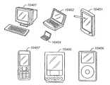
다른 실시예에서는, 상술한 실시예들에 따른 통합 LCD 터치 스크린을 결합하는 전자 장치가 제공된다. 전자 장치는 데스크톱 컴퓨터, 태블릿 컴퓨터, 및 노트북 컴퓨터의 형태를 취할 수 있다. 전자 장치는 또한 핸드헬드 컴퓨터, PDA(personal digital assistant), 미디어 플레이어, 및 휴대용 전화기(mobile telephone)의 형태를 취할 수 있다. 일부 실시예에서, 장치는 전술한 것 중 하나 이상, 예를 들면, 휴대용 전화기 및 미디어 플레이어를 포함할 수 있다.In another embodiment, an electronic device is provided that incorporates an integrated LCD touch screen according to the embodiments described above. Electronic devices may take the form of desktop computers, tablet computers, and notebook computers. The electronic device may also take the form of a handheld computer, a personal digital assistant, a media player, and a mobile telephone. In some embodiments, the device may include one or more of the foregoing, such as a portable telephone and a media player.
본 발명은 첨부 도면들과 함께 다음의 설명을 참조함으로써 가장 잘 이해될 수 있다.
도 1은 멀티포인트 감지 배열을 도시한다.
도 2는 멀티포인트 감지 시스템 상의 다수의 콘택트 패치들(contact patches)을 도시한다.
도 3은 상호 커패시턴스(mutual capacitance) 회로의 단순화된 개략도를 도시한다.
도 4는 멀티포인트 감지 배열을 동작시키는 프로세스를 도시한다.
도 5는 LTPS 반투과반사형(transflective) 서브픽셀에 대한 대표적인 레이아웃을 도시한다.
도 6은 위로부터 및 측면으로부터 본 LTPS의 단순화된 모델을 도시한다.
도 7은 서브픽셀에 대한 회로도를 도시하고 어느 글라스 기판 상에 컴포넌트들이 제조되는지를 보여준다.
도 8은 LCD를 제조하는 기본적인 프로세스 흐름을 도시한다.
도 9는 완성된 소형 사이즈 LCD 모듈을 도시한다.
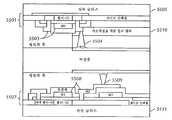
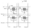
도 10은 개별 터치 드라이버 및 LCD 드라이버 칩들을 갖는 터치 스크린 LCD의 블록도를 도시한다.
도 11은 통합 LCD 및 터치 드라이버 칩을 갖는 터치 스크린 LCD의 블록도를 도시한다.
도 12는 터치 스크린 LCD의 기본 스택업(stackup)을 도시한다.
도 13은 터치 스크린 LCD의 대안 실시예를 도시한다.
도 14는 전극 패턴을 도시한다.
도 15는 터치 스크린 LCD의 스택업도(stackup diagram) 실시예를 도시한다.
도 16은 도 15에서 도시된 터치 스크린 LCD의 터치 픽셀 회로를 도시한다.
도 17은 플라스틱 커버에 의해 보호되는 터치 감지층을 도시한다.
도 18은 터치 스크린의 영역에 대한 출력 게이트들의 연결된 세트(linked set) 및 출력 컬럼을 도시한다.
도 19는 터치 스크린 LCD의 터치 픽셀의 레이아웃을 도시한다.
도 20은 터치 스크린 LCD의 일 실시예에 대한 스택업도를 도시한다.
도 21은 터치 센서 어레이를 도시한다.
도 22는 케이블링 및 서브시스템 배치의 상면도 및 측면도를 갖는, 컨셉트 A 및 B에 대한 물리적 구현을 도시한다.
도 23은 하부 글라스 컴포넌트들의 하나의 가능한 아키텍처를 보여주는 고레벨 블록도를 도시한다.
도 24는 신장된 도전성 도트들을 도시한다.
도 25는 터치/LCD 드라이버 통합 회로에 대한 고레벨 블록도를 도시한다.
도 26은 여기서 설명된 다양한 LCD 실시예들에서 사용하기 위한 연성 인쇄 회로(flexible printed circuit)를 도시한다.
도 27은 동시의 디스플레이 업데이팅 및 터치 스캐닝을 위한 프로세스를 도시한다.
도 28은 개회로 VCST 터치 구동 옵션을 도시한다.
도 29는 구동-VCST 터치 구동 옵션을 도시한다.
도 30은 터치 감지 및 LCD VCOM 변조 양쪽 모두를 위해 터치 구동이 이용되는 상황에 대한 전기적 모델을 도시한다.
도 31은 도전성 도트들을 통하여 양쪽의 Cst 라인들에 VSTM을 접속하는 것을 도시한다.
도 32는 터치 스크린 LCD에 대한 제조 프로세스 흐름을 도시한다.
도 33은 터치 자극 신호로서 VCOM의 1-라인 반전(one-line inversion)을 이용하는 것을 도시한다.
도 34는 터치 스크린 LCD의 대안 실시예에 대한 스택업도를 도시한다.
도 35는 터치 스크린 LCD에 대한 제조 프로세스 흐름을 도시한다.
도 36은 터치 구동층 대신에 도전성 블랙 매트릭스를 이용하는 실시예를 도시한다.
도 37은 터치 스크린 LCD의 실시예에 대한 회로도를 도시한다.
도 38은 터치 스크린 LCD에 대한 스택업도를 도시한다.
도 39는 터치 스크린 LCD의 디스플레이 픽셀들의 한 로우씩의 업데이트(row-by-row update)를 도시한다.
도 40은 터치 스크린 LCD 내의 터치 감응(touch sensitlve) 디스플레이 로우들의 세트에 대한 터치 감지 프로세스를 도시한다.
도 41은 터치 스크린 LCD의 상이한 영역들에 위치하는 3개의 픽셀들에 대한 터치들을 검출하는 프로세스를 도시한다.
도 42는 터치 스크린 LCD의 다른 실시예의 회로도를 도시한다.
도 43은 도 42에서 도시된 실시예의 스택업도를 도시한다.
도 44는 터치 감지층 대신에 도전성 블랙 매트릭스를 이용하는 실시예를 도시한다.
도 45는 터치 스크린 LCD의 다른 실시예의 스택업도를 도시한다.
도 46은 도 55에서 도시된 실시예의 상면도를 도시한다.
도 47은 터치 스크린 LCD의 다른 실시예를 도시한다.
도 48은 도 47의 실시예의 등가 회로를 도시한다.
도 49는 도 47-48의 실시예에서 터치 감지를 위해 이용될 수 있는 파형들을 도시한다.
도 50은 도 47의 실시예에 대한 터치 스크린 통합의 추가 양태들을 도시한다.
도 51은 터치 스크린 LCD의 다른 실시예를 도시한다.
도 52는 도 51 및 53의 실시예에서 터치 감지를 위해 이용될 수 있는 파형들을 도시한다.
도 53은 도 51의 실시예의 등가 회로를 도시한다.
도 54는 도 51의 실시예에 대한 터치 스크린 통합의 추가 양태들을 도시한다.
도 55는 터치 스크린 LCD의 스택업도를 도시한다.
도 56은 터치 스크린 LCD를 업데이트하는 프로세스를 도시한다.
도 57은 터치 스크린 LCD의 실시예에 대한 스택업도를 도시한다.
도 58은 터치 스크린 LCD의 실시예에 대한 스택업도를 도시한다.
도 59는 독립적으로 업데이트되거나 터치-스캔될 수 있는 3개의 영역들로 분할된 예시적인 LCD 디스플레이를 도시한다.
도 60은 3개의 영역들을 갖는 터치 스크린 LCD의 업데이트 및 터치-스캐닝을 도시한다.
도 61은 터치 스크린 LCD에 대한 전극 레이아웃을 도시한다.
도 62는 터치 스크린 LCD에 대한 회로 컴포넌트들을 도시한다.
도 63은 터치 스크린 LCD에 대한 업데이트 배열의 스냅숏을 도시한다.
도 64는 블랙 매트릭스의 배후에 완전히 또는 부분적으로 숨겨질 수 있는 ITO 내의 금속 라인들 및 갭들을 도시한다.
도 65는 터치 스크린 LCD에 대한 스택업도를 도시한다.
도 66은 3개의 영역들로 분할된 터치 스크린 LCD를 도시한다.
도 67은 터치 스크린 LCD에서 디스플레이 업데이트 및 터치-스캐닝을 수행하는 프로세스를 도시한다.
도 68은 터치 스크린 LCD를 3개의 영역들로 분할하는 ITO 레이아웃 및 배선(wiring)을 도시한다.
도 69는 가드 트레이스들을 포함하는 터치 스크린 LCD의 영역의 상면도 및 단면도를 도시한다.
도 70은 가드 트레이스들을 포함하지 않는 터치 스크린 LCD의 영역의 상면도 및 단면도를 도시한다.
도 71은 6개의 터치 픽셀들 및 그들의 신호 배선을 포함하는 예시적인 디스플레이의 영역을 도시한다.
도 72는 터치 스크린 LCD의 다른 실시예에 대한 스택업도를 도시한다.
도 73은 터치 스크린 LCD의 다른 실시예에 대한 스택업도를 도시한다.
도 74는 터치 스크린 LCD에 대한 VCOM 신호 결합을 강조하는 회로도를 도시한다.
도 75는 예시적인 디스플레이를 도시한다.
도 76은 터치 스크린 LCD에 대한 가능한 스캔 패턴을 도시한다.
도 77은 도 79의 실시예에 대한 회로도를 도시한다.
도 78은 세그먼트 ITO 층들을 도시한다.
도 79는 터치 스크린 LCD의 다른 실시예에 대한 스택업도를 도시한다.
도 80은 도 79의 실시예에 대한 결합된 배선 및 스택업도를 도시한다.
도 81은 도 79의 실시예의 물리적 실현을 도시한다.
도 82는 IPS(in-plane switching) LCD 셀들을 도시한다.
도 83은 IPS LCD 셀들에 대한 전극들의 구성을 도시한다.
도 84는 IPS 기반 터치 스크린 LCD의 실시예에 대한 회로도를 도시한다.
도 85는 도 84에 대응하는 스택업도를 도시한다.
도 86은 IPS 기반 터치 스크린 LCD의 다른 실시예에 대한 스택업도를 도시한다.
도 87은 컨셉트 F에 대한 스택업도, IPS 기반 터치 스크린 LCD의 실시예를 도시한다.
도 88은 도 87의 실시예에 대응하는 스택업도를 도시한다.
도 89는 올 글라스(all glass) 터치 스크린 LCD의 측면도를 도시한다.
도 90은 플라스틱 층을 포함하는 터치 스크린 LCD의 측면도를 도시한다.
도 91은 다중 플라스틱 층들을 갖는 터치 스크린을 도시한다.
도 92는 PET 층을 통한 접속을 갖는 2개의 측면 상에 패터닝된 PET 층을 갖는 터치 스크린을 도시한다.
도 93은 조합 PET/글라스 터치 스크린을 도시한다.
도 94는 터치 스크린 LCD 장치 어셈블리를 도시한다.
도 95는 투명한 플라스틱 하우징의 내면 상에 패터닝된 터치 층을 갖는 터치 LCD를 도시한다.
도 96은 터치 스크린 LCD와 함께 이용될 수 있는 패터닝된 PET 기판을 도시한다.
도 97은 도 96의 PET 기판에 접합된 연성 인쇄 회로를 도시한다.
도 98은 도 97의 어셈블리에 부착된 커버를 도시한다.
도 99는 레벨 시프터/디코더 칩 온 글라스(chip on glass)의 단순화된 도면을 도시한다.
도 100은 변경된 터치/LCD 드라이버 및 주변 트랜지스터 회로를 도시한다.
도 101은 완전 통합된 터치/LCD 드라이버의 단순화된 블록도를 도시한다.
도 102는 터치 스크린 LCD의 응용을 도시한다.
도 103은 터치 스크린을 통합하는 컴퓨터 시스템의 블록도를 도시한다.
도 104는 본 발명에 따른 터치 스크린 LCD와 함께 사용될 수 있는 각종 전자 장치 및 컴퓨터 시스템 폼 팩터들을 도시한다.
도 105는 복수의 터치 감지 컬럼들을 형성하도록 접속된 복수의 IPS LCD 서브픽셀들을 도시한다.
도 106은 복수의 터치 감지 로우들을 형성하도록 접속된 복수의 IPS LCD 서브픽셀들을 도시한다.
도 107은 통합 터치 감지를 갖는 IPS LCD를 도시한다.The invention can be best understood by reference to the following description in conjunction with the accompanying drawings.
1 illustrates a multipoint sensing arrangement.
2 shows a number of contact patches on a multipoint sensing system.
3 shows a simplified schematic diagram of a mutual capacitance circuit.
4 shows a process for operating a multipoint sensing arrangement.
5 shows an exemplary layout for LTPS transflective subpixels.
6 shows a simplified model of LTPS seen from above and from the side.
7 shows a circuit diagram for a subpixel and shows on which glass substrate components are fabricated.
8 shows a basic process flow for manufacturing an LCD.
9 shows a completed small size LCD module.
10 shows a block diagram of a touch screen LCD with separate touch driver and LCD driver chips.
11 shows a block diagram of a touch screen LCD with integrated LCD and touch driver chip.
12 shows a basic stackup of a touch screen LCD.
13 illustrates an alternative embodiment of a touch screen LCD.
14 shows the electrode pattern.
FIG. 15 illustrates a stackup diagram embodiment of a touch screen LCD.
FIG. 16 illustrates a touch pixel circuit of the touch screen LCD shown in FIG. 15.
17 shows a touch sensitive layer protected by a plastic cover.
18 shows a linked set of output gates and an output column for an area of the touch screen.
19 shows a layout of touch pixels of a touch screen LCD.
20 illustrates a stackup diagram for one embodiment of a touch screen LCD.
21 shows a touch sensor array.
FIG. 22 shows the physical implementation for Concepts A and B, with top and side views of cabling and subsystem placement.
FIG. 23 shows a high level block diagram showing one possible architecture of the bottom glass components.
24 illustrates elongated conductive dots.
25 shows a high level block diagram for a touch / LCD driver integrated circuit.
FIG. 26 illustrates a flexible printed circuit for use in the various LCD embodiments described herein.
27 shows a process for simultaneous display updating and touch scanning.
28 shows the open circuit VCST touch drive option.
29 illustrates a Drive-VCST Touch Drive option.
30 shows an electrical model for the situation where touch drive is used for both touch sensing and LCD VCOM modulation.
31 illustrates connecting VSTM to both Cst lines through conductive dots.
32 shows a manufacturing process flow for a touch screen LCD.
33 illustrates using one-line inversion of VCOM as the touch stimulus signal.
34 illustrates a stackup diagram for an alternative embodiment of a touch screen LCD.
35 shows a manufacturing process flow for a touch screen LCD.
36 illustrates an embodiment using a conductive black matrix instead of a touch drive layer.
37 shows a circuit diagram for an embodiment of a touch screen LCD.
38 shows a stackup diagram for a touch screen LCD.
FIG. 39 illustrates a row-by-row update of display pixels of a touch screen LCD.
40 illustrates a touch sensing process for a set of touch sensitlve display rows in a touch screen LCD.
41 shows a process for detecting touches for three pixels located in different regions of a touch screen LCD.
42 shows a circuit diagram of another embodiment of a touch screen LCD.
FIG. 43 shows a stackup diagram of the embodiment shown in FIG. 42.
44 illustrates an embodiment using a conductive black matrix instead of a touch sensitive layer.
45 illustrates a stackup diagram of another embodiment of a touch screen LCD.
FIG. 46 shows a top view of the embodiment shown in FIG. 55.
47 illustrates another embodiment of a touch screen LCD.
FIG. 48 shows an equivalent circuit of the embodiment of FIG. 47.
FIG. 49 illustrates waveforms that can be used for touch sensing in the embodiment of FIGS. 47-48.
FIG. 50 illustrates further aspects of touch screen integration for the embodiment of FIG. 47.
51 illustrates another embodiment of a touch screen LCD.
FIG. 52 illustrates waveforms that may be used for touch sensing in the embodiment of FIGS. 51 and 53.
FIG. 53 shows an equivalent circuit of the embodiment of FIG. 51.
FIG. 54 illustrates additional aspects of touch screen integration for the embodiment of FIG. 51.
55 shows a stackup diagram of a touch screen LCD.
56 shows a process for updating the touch screen LCD.
57 shows a stackup diagram for an embodiment of a touch screen LCD.
58 shows a stackup diagram for an embodiment of a touch screen LCD.
FIG. 59 shows an exemplary LCD display divided into three areas that can be updated or touch-scanned independently.
60 shows an update and touch-scanning of a touch screen LCD with three regions.
61 shows the electrode layout for a touch screen LCD.
62 shows circuit components for a touch screen LCD.
63 shows a snapshot of the update arrangement for a touch screen LCD.
64 shows metal lines and gaps in ITO that may be completely or partially hidden behind a black matrix.
65 shows a stackup diagram for a touch screen LCD.
66 shows a touch screen LCD divided into three regions.
67 shows a process for performing display update and touch-scanning on a touch screen LCD.
FIG. 68 shows the ITO layout and wiring for dividing the touch screen LCD into three regions.
69 shows a top view and a cross sectional view of an area of a touch screen LCD including guard traces.
70 shows a top view and cross-sectional view of an area of a touch screen LCD that does not include guard traces.
71 shows an area of an exemplary display that includes six touch pixels and their signal wiring.
72 illustrates a stackup diagram for another embodiment of a touch screen LCD.
73 illustrates a stackup diagram for another embodiment of a touch screen LCD.
74 shows a circuit diagram that highlights VCOM signal coupling for a touch screen LCD.
75 shows an example display.
76 shows a possible scan pattern for a touch screen LCD.
FIG. 77 shows a circuit diagram for the embodiment of FIG. 79.
78 shows segment ITO layers.
79 illustrates a stackup diagram for another embodiment of a touch screen LCD.
FIG. 80 illustrates a combined wiring and stackup diagram for the embodiment of FIG. 79.
FIG. 81 illustrates a physical realization of the embodiment of FIG. 79.
82 illustrates in-plane switching LCD cells.
83 shows the configuration of the electrodes for the IPS LCD cells.
84 shows a circuit diagram for an embodiment of an IPS-based touch screen LCD.
85 illustrates a stackup diagram corresponding to FIG. 84.
86 shows a stackup diagram for another embodiment of an IPS-based touch screen LCD.
FIG. 87 shows a stackup diagram for Concept F, an embodiment of an IPS based touch screen LCD.
FIG. 88 illustrates a stackup diagram corresponding to the embodiment of FIG. 87.
89 shows a side view of an all glass touch screen LCD.
90 illustrates a side view of a touch screen LCD that includes a plastic layer.
91 shows a touch screen with multiple plastic layers.
92 shows a touch screen with a PET layer patterned on two sides with a connection through the PET layer.
93 shows a combination PET / glass touch screen.
94 illustrates a touch screen LCD device assembly.
95 illustrates a touch LCD with a touch layer patterned on the inner surface of a transparent plastic housing.
96 illustrates a patterned PET substrate that may be used with a touch screen LCD.
FIG. 97 illustrates a flexible printed circuit bonded to the PET substrate of FIG. 96.
FIG. 98 shows a cover attached to the assembly of FIG. 97.
FIG. 99 shows a simplified diagram of a level shifter / decoder chip on glass.
100 illustrates a modified touch / LCD driver and peripheral transistor circuit.
101 shows a simplified block diagram of a fully integrated touch / LCD driver.
102 illustrates an application of a touch screen LCD.
103 shows a block diagram of a computer system incorporating a touch screen.
104 illustrates various electronic device and computer system form factors that may be used with a touch screen LCD in accordance with the present invention.
105 shows a plurality of IPS LCD subpixels connected to form a plurality of touch sensing columns.
106 illustrates a plurality of IPS LCD subpixels connected to form a plurality of touch sense rows.
107 illustrates an IPS LCD with integrated touch sensing.
다음의 설명은 어떤 당업자라도 본 발명을 만들고 사용할 수 있게 하기 위해 제공되며, 특정 응용 및 그의 요건들과 관련하여 제공된다. 개시된 실시예들에 대한 다양한 변경들은 당업자들이 쉽사리 알 수 있을 것이고, 여기서 정의된 일반 원리들은 본 발명의 정신 및 범위에서 일탈하지 않고 다른 실시예들 및 응용들에 적용될 수 있다. 따라서, 본 발명은 제시된 실시예들에 제한되지 않고, 청구항들과 일관된 최광의 범위가 주어져야 할 것이다.The following description is presented to enable any person skilled in the art to make and use the invention, and is provided with regard to specific applications and requirements thereof. Various modifications to the disclosed embodiments will be readily apparent to those skilled in the art, and the generic principles defined herein may be applied to other embodiments and applications without departing from the spirit and scope of the invention. Thus, the present invention should not be limited to the embodiments shown but should be accorded the widest scope consistent with the claims.
1.One.LCDLCD 및 터치 감지 배경 기술 And touch sensing background technology
여기서는 터치 감지 기술을 액정 디스플레이들에 통합하는 기법들이 개시된다.Disclosed herein are techniques for integrating touch sensing technology into liquid crystal displays.
당업자에게 알려진 바와 같이, LCD는 복수의 층들, 가장 기본적으로는, 상부 글라스, 액정, 및 하부 글라스를 포함한다. 상부 및 하부 글라스들은 특정 디스플레이 픽셀에 대한 액정을 포함하는 셀들의 경계를 제공하도록 패터닝될 수 있다. 상부 및 하부 글라스들은 또한 액정의 배향을 조작함으로써 픽셀의 컬러 및 휘도를 제어하기 위하여 액정 셀들을 가로지르는 전압이 변경되도록 하는 박막 트랜지스터들 및 도전성 재료의 다양한 층들로 패터닝될 수 있다.As is known to those skilled in the art, the LCD comprises a plurality of layers, most basically, top glass, liquid crystal, and bottom glass. The upper and lower glasses can be patterned to provide a border of cells that contain liquid crystal for a particular display pixel. The upper and lower glasses can also be patterned into various layers of thin film transistors and conductive material such that the voltage across the liquid crystal cells is changed to control the color and brightness of the pixel by manipulating the orientation of the liquid crystal.
참고로 통합된 출원들에서 설명된 바와 같이, 터치 표면, 및 구체적으로는, 멀티 터치 가능한(multi-touch capable) 투명 터치 표면은 일련의 층들로부터 형성될 수 있다. 이 일련의 층들은 복수의 터치 감응 전극들이 그 위에 배치되어 있을 수 있는, 적어도 하나의 기판, 예를 들면, 글라스를 포함할 수 있다. 예를 들면, 상호 커패시턴스(mutual capacitance) 배열은 비도전층, 즉, 글라스에 의해 분리된 복수의 구동 전극들 및 복수의 감지 전극들을 포함할 수 있다. 구동 및 감지 전극들 간의 용량 결합은 도전성 물체(예를 들면, 사용자의 손가락)에 의해 영향을 받을 수 있다. 이 용량 결합의 변화는 특정 터치의 위치, 형상, 사이즈, 움직임, ID(identity) 등을 결정하는 데 이용될 수 있다. 그 후 이들 파라미터들은 컴퓨터 또는 기타 전자 장치의 동작을 제어하도록 해석될 수 있다. 후술되는 자기 커패시턴스(self capacitance) 배열들도 당업자에게 알려져 있다.As described in the incorporated applications for reference, a touch surface, and specifically a multi-touch capable transparent touch surface, may be formed from a series of layers. This series of layers may comprise at least one substrate, for example glass, in which a plurality of touch sensitive electrodes may be disposed thereon. For example, the mutual capacitance arrangement may comprise a plurality of drive electrodes and a plurality of sensing electrodes separated by a non-conductive layer, ie, glass. Capacitive coupling between the drive and sense electrodes can be affected by a conductive object (eg, a user's finger). This change in capacitive coupling can be used to determine the location, shape, size, movement, identity, etc. of a particular touch. These parameters can then be interpreted to control the operation of the computer or other electronic device. Self capacitance arrangements, described below, are also known to those skilled in the art.
LCD 및 터치 센서의 층상 구조(layered structure)를 통합함으로써, 다양한 이익들이 달성될 수 있다. 이 통합은 상술한 층상 구조들을 조합하거나 인터리브(interleave)하는 것을 포함할 수 있다. 통합은 중복되는 구조들을 제거하고 및/또는 이중 목적(예를 들면, 터치 기능을 위한 하나의 목적 및 디스플레이 기능을 위한 다른 목적)를 찾아내는 것을 더 포함할 수 있다. 이는 일부 층들이 제거되도록 할 수 있고, 이는 터치 스크린 LCD의 비용 및 두께를 저감시킬 수 있을 뿐만 아니라, 제조를 단순화할 수 있다. 각종의 상이한 배열들이 가능하고, 그 중 일부는 여기서 더 상세히 논의된다.By integrating the layered structure of the LCD and touch sensor, various benefits can be achieved. This integration may include combining or interleaving the layer structures described above. The integration may further include eliminating redundant structures and / or finding a dual purpose (eg, one purpose for touch functionality and another for display functionality). This may allow some layers to be removed, which may reduce the cost and thickness of the touch screen LCD, as well as simplify the manufacturing. Various different arrangements are possible, some of which are discussed in more detail herein.
구체적으로, 통합 터치 스크린 LCD의 다양한 실시예들이 이하에서 논의된다. 그러나, 당업자는 이 도면들과 관련하여 여기서 주어지는 상세한 설명은 예시적인 것으로 총망라한 것이 아니며, 이들 실시예들에 대한 많은 변형들이 가능하다는 것을 알 것이다. 또한, 비록 개시된 실시예들 중 다수는 멀티 터치 가능한 배열들에 관한 것이지만, 그 교시 내용 중 다수는 싱글 터치 디스플레이에도 적용될 수 있다.Specifically, various embodiments of the integrated touch screen LCD are discussed below. However, those skilled in the art will appreciate that the detailed description given herein in connection with these figures is illustrative and not exhaustive, and that many variations on these embodiments are possible. Further, although many of the disclosed embodiments relate to multi-touchable arrangements, many of the teachings may be applied to single touch displays.
1.1. 멀티 터치 감지1.1. Multi-touch detection
복수의 동시의 또는 거의 동시의 터치 이벤트들을 인지하는 것은 도 1에서 도시된 바와 같은 멀티 터치 감지 배열들에 의해 달성될 수 있다. 멀티 터치 감지 배열(100)은 터치 감응 표면(101)에 걸쳐서, 동시에, 거의 동시에, 상이한 시점들에서, 또는 어떤 시간 기간에 걸쳐서, 복수의 터치 속성들(예를 들면, ID(identification), 위치, 속도, 사이즈, 형상, 및 크기)을 검출 및 모니터할 수 있다. 터치 감응 표면(101)은 실질적으로 서로 독립적으로 기능하고 터치 감응 표면 상의 상이한 포인트들을 나타내는 복수의 센서 포인트들, 좌표들, 또는 노드들(102)을 제공할 수 있다. 감지 포인트들(102)은 격자(grid) 또는 픽셀 어레이로 배치될 수 있고, 각 감지 포인트는 동시에 신호를 생성할 수 있다. 감지 포인트들(102)은 터치 감응 표면(101)을 좌표계, 예를 들면, 직교 좌표계 또는 극 좌표계로 매핑하는 것으로 간주될 수 있다.Recognizing a plurality of simultaneous or near simultaneous touch events can be accomplished by multi-touch sensing arrangements as shown in FIG. 1. The
터치 감응 표면은, 예를 들면, 태블릿 또는 터치 스크린의 형태로 될 수 있다. 터치 스크린을 생성하기 위하여, 커패시턴스 감지 포인트들 및 다른 관련된 전기적 구조들이 인듐 주석 산화물(ITO)과 같은 실질적으로 투명한 도전성 매체를 이용하여 형성될 수 있다. 감지 포인트들(102)의 개수 및 구성은 변경될 수 있다. 감지 포인트들(102)의 개수는 일반적으로 원하는 해상도 및 감도에 좌우된다. 터치 스크린 응용에서, 감지 포인트들(102)의 개수는 또한 터치 스크린의 원하는 투명도에 좌우될 수 있다.The touch sensitive surface can be, for example, in the form of a tablet or touch screen. To generate the touch screen, capacitance sense points and other related electrical structures can be formed using a substantially transparent conductive medium such as indium tin oxide (ITO). The number and configuration of the sensing points 102 can vary. The number of sense points 102 generally depends on the desired resolution and sensitivity. In touch screen applications, the number of sensing points 102 may also depend on the desired transparency of the touch screen.
아래에서 더 상세히 설명되는 것과 같은, 멀티 터치 감지 배열을 이용하면, 멀티 터치 센서(101)의 노드들(102)에서 생성된 신호들은 특정 시점에서의 터치들의 이미지를 생성하는 데 이용될 수 있다. 예를 들면, 터치 감응 표면(101)과 접촉하거나 그에 근접하는 각 물체(예를 들면, 손가락, 스타일러스 등)는 도 2에서 도시된 바와 같이 콘택트 패치 영역(contact patch area)(201)을 생성할 수 있다. 각 콘택트 패치 영역(201)은 몇 개의 노드들(102)을 커버할 수 있다. 커버된 노드들(202)은 물체를 검출할 수 있지만, 나머지 노드들(102)은 그렇지 않다. 그 결과, 터치 표면 평면의 픽셀화 이미지(pixelated image)(터치 이미지, 멀티 터치 이미지, 또는 근접 이미지라고 불릴 수 있음)가 형성될 수 있다. 각 콘택트 패치 영역(201)에 대한 신호들은 함께 그룹화될 수 있다. 각 콘택트 패치 영역(201)은 각 포인트에서의 터치의 양에 기초하여 고 포인트(high point) 및 저 포인트(low point)를 포함할 수 있다. 콘택트 패치 영역(201)의 형상뿐만 아니라, 이미지 내의 고 포인트 및 저 포인트는 서로 근접해 있는 콘택트 패치 영역들(201)을 구별하는 데 이용될 수 있다. 더욱이, 현 이미지를 이전 이미지와 비교하여 물체들이 시간에 걸쳐서 어떻게 움직일 수 있는지, 및 그의 결과로 호스트 장치에서 어떤 대응하는 액션이 수행되어야 하는지를 결정할 수 있다.Using a multi-touch sensing arrangement, as described in more detail below, the signals generated at the
저항성(resistive), 용량성(capacitive), 광학(optical) 등을 포함하여, 다수의 상이한 감지 기술들이 이들 감지 배열과 관련하여 이용될 수 있다. 커패시턴스 기반 감지 배열에서는, 물체가 터치 감응 표면(101)에 접근할 때, 그 물체와 그 물체에 근접하는 감지 포인트들(102) 사이에 작은 커패시턴스가 형성된다. 이 작은 커패시턴스에 의해 야기되는 감지 포인트들(102) 각각에서의 커패시턴스의 변화들을 검출함으로써, 그리고 감지 포인트들의 위치를 알아차림으로써, 감지 회로(103)는 복수의 터치들을 검출 및 모니터할 수 있다. 이 용량성 감지 노드들은 자기 커패시턴스 또는 상호 커패시턴스에 기초할 수 있다.Many different sensing techniques can be used in connection with these sensing arrangements, including resistive, capacitive, optical, and the like. In a capacitance based sensing arrangement, when an object approaches the touch
자기 커패시턴스 시스템에서는, 어떤 기준, 예를 들면, 접지에 대하여 감지 포인트의 "자기" 커패시턴스가 측정된다. 감지 포인트들(102)은 공간적으로 분리된 전극들일 수 있다. 이 전극들은 도전성 트레이스들(105a(구동 라인들) 및 105b(감지 라인들))에 의해 구동 회로(104) 및 감지 회로(103)에 결합될 수 있다. 일부 자기 커패시턴스 시스템에서는, 각 전극에의 단일 도전성 트레이스가 구동 라인 및 감지 라인 양쪽 모두로서 이용될 수 있다.In a magnetic capacitance system, the "magnetic" capacitance of the sense point is measured with respect to some reference, for example, ground. The sense points 102 may be spatially separated electrodes. These electrodes can be coupled to the
상호 커패시턴스 시스템에서는, 제1 전극과 제2 전극 간의 "상호" 커패시턴스가 측정될 수 있다. 상호 커패시턴스 감지 배열에서, 감지 포인트들은 공간적으로 분리된 라인들을 형성하는 패터닝된 도체들의 교차점들에 의해 형성될 수 있다. 예를 들면, 구동 라인들(105a)은 제1 층 상에 형성될 수 있고 감지 라인들(105b)은 제2 층(105b) 상에 형성될 수 있어, 구동 라인들 및 감지 라인들은 감지 포인트들(102)에서 서로 가로지르거나 "교차"할 수 있다. 상이한 층들은 상이한 기판들, 동일 기판의 상이한 측면들, 또는 어떤 유전성 분리(dielectric separation)를 갖는 기판의 동일한 측면일 수 있다. 구동 라인들과 감지 라인들 간의 분리 때문에, 각 "교차점"에 용량 결합 노드가 있을 수 있다.In a mutual capacitance system, the "mutual" capacitance between the first electrode and the second electrode can be measured. In a mutual capacitance sensing arrangement, the sensing points can be formed by the intersections of the patterned conductors forming spatially separated lines. For example, the
구동 및 감지 라인들의 배열은 변화할 수 있다. 예를 들면, (도시된) 직교 좌표계에서, 구동 라인들은 수평 로우들로서 형성될 수 있고, 감지 라인들은 수직 컬럼들로서 형성될 수 있어(또는 반대로), 별개의 x 및 y 좌표들을 갖는 것으로 간주될 수 있는 복수의 노드들을 형성한다. 대안적으로, 극 좌표계에서, 감지 라인들은 복수의 동심원일 수 있고 구동 라인들은 방사상으로 연장하는 라인들일 수 있어(또는 반대로), 별개의 반경 및 각도 좌표들을 갖는 것으로 간주될 수 있는 복수의 노드들을 형성한다. 어느 쪽의 경우든, 구동 라인들(105a)은 구동 회로(104)에 접속될 수 있고, 감지 라인들(105b)은 감지 회로(103)에 접속될 수 있다.The arrangement of the drive and sense lines can vary. For example, in a Cartesian coordinate system (shown), the drive lines can be formed as horizontal rows and the sense lines can be formed as vertical columns (or vice versa) and can be considered to have separate x and y coordinates. Form a plurality of nodes. Alternatively, in the polar coordinate system, the sense lines can be a plurality of concentric circles and the drive lines can be radially extending lines (or vice versa), thereby generating a plurality of nodes that can be considered to have separate radius and angular coordinates. Form. In either case, the
동작 중에, 구동 신호(예를 들면, 주기적인 전압)가 각 구동 라인(105a)에 인가될 수 있다. 구동될 경우, 구동 라인(105a) 상의 영향을 받은 전하는 노드들(102)을 통하여 교차하는 감지 라인들(105b)에 용량 결합할 수 있다. 이는 감지 라인들(105b)에서 검출 가능한, 측정 가능한 전류 및/또는 전압을 일으킬 수 있다. 구동 신호와 감지 라인들(105b) 상에 나타나는 신호 간의 관계는 구동 및 감지 라인들을 결합하는 커패시턴스의 함수일 수 있고, 이는 전술한 바와 같이, 노드(102)에 근접하는 물체에 의해 영향을 받을 수 있다. 커패시턴스 감지 회로(또는 회로들)(103)는 아래에서 더 상세히 설명되는 바와 같이 감지 라인들(105b)을 감지할 수 있고 각 노드에서의 커패시턴스를 결정할 수 있다.In operation, a drive signal (eg, a periodic voltage) can be applied to each
위에서 논의된 바와 같이, 구동 라인들(105a)은, 다른 구동 라인들이 접지되어 있는 동안에, 한 번에 하나씩 구동될 수 있다. 이 프로세스는 모든 구동 라인들이 구동될 때까지 각 구동 라인(105a)에 대하여 반복될 수 있고, 감지된 결과로부터 터치 이미지(커패시턴스에 기초함)가 구성될 수 있다. 일단 모든 라인들(105a)이 구동되면, 시퀀스는 일련의 터치 이미지들을 형성하도록 반복할 수 있다. 그러나, 본 발명의 일부 실시예에서는, 2007년 1월 3일에 출원된, "Simultaneous Sensing Arrangement"라는 명칭의, 미국 특허 출원 11/619,466호에서 설명된 바와 같이, 복수의 구동 라인들이 실질적으로 동시에 또는 거의 동시에 구동될 수 있다.As discussed above, the
도 3은 전술한 배열에 대응하는 상호 커패시턴스 회로(300)의 단순화된 개략도를 도시한다. 상호 커패시턴스 회로(300)는 구동 라인(105a) 및 감지 라인(105b)을 포함할 수 있고, 이들은 공간적으로 분리됨으로써 용량 결합 노드(102)를 형성할 수 있다. 구동 라인(105a)은 전압원(301)으로 표현된 구동 회로(104)에 전기적으로(즉, 도전성 있게) 결합될 수 있다. 감지 라인(105b)은 커패시턴스 감지 회로(803)에 전기적으로 결합될 수 있다. 구동 라인(105a) 및 감지 라인(105b) 양쪽 모두는, 일부 경우에, 얼마간의 기생 커패시턴스(302)를 포함할 수 있다.3 shows a simplified schematic diagram of a
전술한 바와 같이, 구동 라인(105a)과 감지 라인(105b)의 교차점에 근접하는 도전성 물체의 부재시에, 노드(102)에서의 용량 결합은 꽤 일정한 상태로 있을 수 있다. 그러나, 전기 도전성 물체(예를 들면, 사용자의 손가락, 스타일러스 등)가 노드(102)에 근접하여 오면, 용량 결합(즉, 로컬 시스템의 커패시턴스)은 변화한다. 이 용량 결합의 변화는 감지 라인(105b)에 의해 운반되는 전류(및/또는 전압)를 변화시킨다. 커패시턴스 감지 회로(103)는 이 커패시턴스 변화 및 노드(102)의 위치를 알아차리고 이 정보를 소정의 형태로 프로세서(106)(도 1)에 보고한다.As discussed above, in the absence of a conductive object proximate to the intersection of
도 1을 참조하여, 감지 회로(103)는 터치 표면(101)으로부터 데이터를 획득하고 그 획득된 데이터를 프로세서(106)에 공급할 수 있다. 일부 실시예에서, 감지 회로(103)는 원시 데이터(raw data)(예를 들면, 각 감지 포인트(102)에 대응하는 커패시턴스 값들의 어레이)를 프로세서(106)에 송신하도록 구성될 수 있다. 다른 실시예에서, 감지 회로(103)는 원시 데이터 자체를 처리하고 처리된 터치 데이터를 프로세서(106)에 전달하도록 구성될 수 있다. 어느 쪽의 경우든, 프로세서는 그 후 그것이 수신하는 데이터를 이용하여 컴퓨터 시스템(107) 및/또는 그 위에서 실행중인 하나 이상의 애플리케이션의 동작을 제어할 수 있다. 이들 라인들을 따르는 다양한 구현들이 위에서 참조된 출원들에서 설명되어 있고, 터치 패드들 및 터치 스크린들을 갖는 각종의 컴퓨터 시스템들을 포함한다.Referring to FIG. 1, the
일부 실시예에서, 감지 회로(103)는 하나 이상의 마이크로컨트롤러를 포함할 수 있고, 그 각각은 하나 이상의 감지 포인트들(102)을 모니터할 수 있다. 마이크로컨트롤러들은 펌웨어와 협력하여 터치 감응 표면(101)로부터의 신호들을 모니터하고, 모니터된 신호들을 처리하고, 이 정보를 프로세서(106)에 보고하는 특수 용도의 집적 회로(ASIC)들일 수 있다. 마이크로컨트롤러들은 또한 디지털 신호 프로세서(DSP)들일 수 있다. 일부 실시예에서, 감지 회로(103)는 각 감지 라인(105b)에서 커패시턴스를 측정하고 측정된 값들을 프로세서(106)에 또는 컴퓨터 시스템(107) 내의 호스트 컨트롤러(도시되지 않음)에 보고하는 하나 이상의 센서 IC들을 포함할 수 있다. 임의의 개수의 센서 IC들이 이용될 수 있다. 예를 들면, 하나의 센서 IC가 모든 라인들에 대하여 이용될 수 있고, 또는 복수의 센서 IC들이 단일 라인 또는 라인들의 그룹에 대하여 이용될 수 있다.In some embodiments,
도 4는 전술한 것과 같은, 멀티 터치 감지 배열을 동작시키기 위한 고레벨 프로세스(400)를 도시한다. 이 프로세스는 블록 401에서 시작하고 여기서는 복수의 감지 포인트들(102)이 구동될 수 있다. 블록 401에 이어서, 프로세스 흐름은 블록 402로 진행할 수 있고, 여기서는 감지 포인트들(102)로부터의 출력들이 판독될 수 있다. 예를 들면, 각 감지 포인트(102)에 대한 커패시턴스 값이 획득될 수 있다. 블록 402에 이어서, 프로세스는 블록 403으로 진행할 수 있고 여기서는 한 시점에서의 터치의 이미지 또는 다른 형태의 데이터(신호 또는 신호들)가 생성될 수 있고 그 후 터치 센서에 접촉하거나 그에 근접하는 물체들이 어디에 위치할 수 있는지를 결정하기 위해 분석될 수 있다. 블록 403에 이어서, 프로세스는 블록 404로 진행할 수 있고, 여기서는 각 물체에 대한 형상, 사이즈, 위치, 방향, 속도, 가속, 압력 등의 하나 이상의 변화를 결정하기 위해 현 이미지 또는 신호가 하나 이상의 과거 이미지들 또는 신호들과 비교될 수 있다. 이 정보는 그 후, 포인트 또는 커서를 움직이는 것으로부터 복잡한 제스처 기반 상호작용에 이르기까지, 컴퓨터 시스템(107)에서 액션을 수행하는 데 이용될 수 있다(단계 405에서).4 shows a
1.2.1.2.반투과반사형Transflective typeLCDLCD
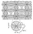
반투과반사형(transflective) LCD와의 터치 감지 기술의 통합을 더 잘 이해하기 위하여, 반투과반사형 LCD에 대한 간략한 소개가 도움이 될 수 있다. 다음은 LTPS(low temperature poly-silicon) 반투과반사형 LCD에서 발견되는 전형적인 서브픽셀 셀에 대한 개관이다.In order to better understand the integration of touch sensing technology with transflective LCDs, a brief introduction to transflective LCDs can be helpful. The following is an overview of typical subpixel cells found in low temperature poly-silicon (LTPS) transflective LCDs.
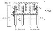
1.2.1. 회로 기초1.2.1. Circuit foundation
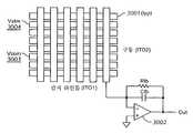
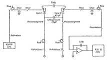
도 5는 LTPS 반투과반사형 서브픽셀(500)에 대한 대표적인 레이아웃을 도시한다. 원하는 그레이 레벨을 나타내는 전압이 데이터 버스(501)에 인가되고 선택 라인(502)이 어서트(assert)될 경우 서브픽셀의 커패시터들 CST 및 CLC에 디스플레이 정보가 전송될 수 있다. 선택 라인(502) 어설션(assertion) 레벨은 게이트 구동 플러스 공급 전압에 가까울 수 있다. 선택 라인(502)이 어서트되는 시간 동안에, VCST(및 도시되지 않은 VCOM) 상의 전압은 일정할 수 있다. 금속, 폴리, 능동(active), 산화물, 및 ITO를 포함하는, 도 5에서 도시된 모든 회로 소자들은 LCD의 하부 글라스 상에 제조될 수 있다.5 shows a representative layout for an
도 6은 상면도(601) 및 측면도(602)를 포함하는, LTPS(low temperature poly-silicon) LCD(600)의 단순화된 모델을 보여준다. 상면도(601)는 디스플레이 영역(604) 및 비디스플레이(non-display) 영역(605) 양쪽 모두에서의 하부 글라스(608) 상의 VCST 라우팅(603)의 투명도(see-through view)를 보여준다. 측면도(602)는 디스플레이의 단면을 보여준다.6 shows a simplified model of a low temperature poly-silicon (LTPS)
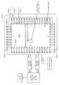
각 디스플레이 로우는 VCST(606) 및 선택(도시되지 않음)을 위한 수평 트레이스들을 포함할 수 있다. 선택 트레이스들은, 도시되지 않은, 폴리실리콘 박막 트랜지스터(p-Si TFT)들로 이루어진 게이트 구동 회로에 접속한다. VCST 트레이스들(606)은 디스플레이 에지로부터 디스플레이 에지까지 연장할 수 있고, 예를 들면, 좌측에 도시된 바와 같이, 함께 접속할 수 있다. VCST 트레이스들은 또한, 도전성 도트(607)를 통하여, 상부 글라스(610) 상의 ITO 평면(609)에 접속할 수 있다. 전형적으로, 각 코너에 하나씩, 4개의 도전성 도트들이 VCOM 평면을 VCOMDrive(611)에 접속하는 데 이용될 수 있다. 도 6은 간소화를 위하여 하나의 도트(607)만을 보여준다. VCST 및 상부 ITO(609)의 전압은 VCOMDrive에 의해 설정될 수 있고, 이 VCOMDrive는 LCD 드라이버 IC(도시되지 않음)에 의해 제공될 수 있다. VCST는 또한 VCOMDrive(611) 이외의 다른 구동원에 접속될 수 있다.Each display row may include VCST 606 and horizontal traces for selection (not shown). The select traces connect to a gate drive circuit made of polysilicon thin film transistors (p-Si TFTs), not shown. The VCST traces 606 may extend from the display edge to the display edge and may connect together, for example, as shown on the left. The VCST traces may also connect to the
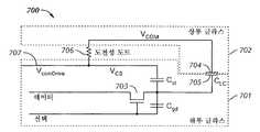
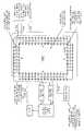
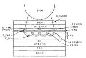
도 7은 서브픽셀에 대한 회로도(700)를 도시하고 어느 글라스 기판 상에 다양한 컴포넌트들이 제조될 수 있는지를 보여준다. 하부 글라스(701)는 모든 TFT 픽셀 회로(703)의 통합을 위한 기판일 수 있다. 이것은 선택 라인 드라이버들 및 제어 로직을 포함할 수 있다. 하부 글라스는 또한 LCD 드라이버(도시되지 않음)와 같은, 칩 온 글라스(COG) 컴포넌트들을 위한 기판으로서 작용할 수도 있다. 커패시터 CLC의 상위 전극(304)은 상부 글라스(702) 상에 있을 수 있다. 전극(704)은 전체 디스플레이 영역을 커버하고 하부 전극(705)에 대한 대향 전극(counter electrode)을 형성하여 CLC를 만드는 ITO 평면일 수 있다. 상위 전극(704)은 또한, 예를 들면, 4개의 코너에 위치하는 도전성 도트들(706)(하나만 도시됨)을 통하여, 하부 글라스(701) 상의 VCOMDrive(707)에 접속할 수 있다.7 shows a circuit diagram 700 for a subpixel and shows on which glass substrate various components can be fabricated. The
1.2.2.1.2.2.VVCOMCOM
액정(LC)을 가로지르는 전압의 DC 성분을 최소화하거나 제거함으로써 일부 바람직하지 못한 이미지 아티팩트들(image artifacts)을 감소시키거나 제거할 수 있다. 그러므로, IC를 가로지르는 전계는 2개의 전계 방향 간의 전체적인 균형을 유지하면서 주기적으로 플립(flip)될 수 있다. 완벽한 전계 균형을 얻는 것은 어려울 수 있고, 이로 인해 불필요한 이미지 아티팩트들을 생성할 수 있는 작은 DC 오프셋들이 생길 수 있다. DC 오프셋들로 인한 깜박임(flicker)을 마스킹하기 위하여, 도트 반전과 같은, 당업자에게 알려진 몇몇 반전 방식들 중 하나가 채용될 수 있다.By minimizing or eliminating the DC component of the voltage across the liquid crystal LC, some undesirable image artifacts may be reduced or eliminated. Therefore, the electric field across the IC can be flipped periodically while maintaining the overall balance between the two field directions. It can be difficult to achieve perfect field balance, which can result in small DC offsets that can create unwanted image artifacts. In order to mask flicker due to DC offsets, one of several inversion schemes known to those skilled in the art, such as dot inversion, may be employed.
1.2.3.1.2.3.VVCOMCOM 변조 Modulation
일부 실시예에서는, 데이터 드라이버들의 전압 범위를 감소시키는 것이 바람직할 수 있다. 그러므로, VCOM ITO 평면 및 VCST 트레이스들은 LC를 가로질러 AC 전압을 생성하기 위해 접지 전압에서 공급 전압 레일까지(from ground to the supply rail) 변조될 수 있다. 그러나, 이것은 이용 가능한 반전 방법들을 프레임 및 라인 타입들만으로 제한할 수 있다.In some embodiments, it may be desirable to reduce the voltage range of the data drivers. Therefore, the VCOM ITO plane and the VCST traces can be modulated from ground voltage to ground supply rail to generate an AC voltage across the LC. However, this may limit the available inversion methods to frame and line types only.
VCOMDrive 요건들은 아주 단순할 수 있다: 그의 전압은 한 로우의 픽셀들에 대하여 전하 전송이 완료되어, 그들의 그레이 레벨들을 설정할 때까지 일정하게 유지될 수 있다. 일단 디스플레이 픽셀들이 설정되면, 서브픽셀 안팎으로의 기생 경로들이 작게 유지된다는 조건으로 VCOMDrive는 LC 상태에 크게 영향을 미치지 않고 변화할 수 있다.VCOM Drive requirements can be quite simple: its voltage can remain constant until charge transfer is complete for a row of pixels to set their gray levels. Once the display pixels are set, the VCOM drive can change without significantly affecting the LC state provided the parasitic paths in and out of the subpixel remain small.
1.2 4. 일정한1.2 4. ConstantVVCOMCOM
VCOM 변조는 LCD와의 터치 감지의 통합을 복잡하게 할 수 있다. 이러한 복잡화를 극복하기 위한 다양한 기법들은 아래에서 논의된다. 액정을 가로지르는 전압의 DC 성분을 최소화하는 대안적인 방법이 채용될 수 있다. 한 가지 그러한 대안적인 방법은, 본원에 참고로 통합되는, J. Hector 및 p. Buchschacher 공저, "Low Power Driving Options for an AMLCD Mobile Display Chipset", SID 02 Digest, pp. 695-697에서 개시되어 있다. 이 대안적인 방법은 VCOM이 일정한 전압에 머무르도록 할 수 있고, 전압 범위가 큰(large-voltage range) 데이터 드라이버를 필요로 하지 않고, 낮은 전력을 소비할 수 있다. 일정한 VCOM을 이용하는 것의 다양한 이점들은 아래에서 설명된다.VCOM modulation can complicate the integration of touch sensing with LCDs. Various techniques for overcoming this complexity are discussed below. Alternative methods may be employed to minimize the DC component of the voltage across the liquid crystal. One such alternative method is described in J. Hector and p. Buchschacher, "Low Power Driving Options for an AMLCD Mobile Display Chipset", SID 02 Digest, pp. 695-697. This alternative approach allows VCOM to stay at a constant voltage, does not require a large-voltage range data driver, and can consume low power. Various advantages of using a constant VCOM are described below.
1.3.1.3.LCDLCD 제조 Produce
LCD 패널들의 제조는 마더 글라스(mother-glass)라 불리는 대형 글라스들 상에서 일괄 프로세스를 이용하여 행해질 수 있다. 2개의 마더 글라스가 이용될 수 있다: 컬러 필터, 블랙 매트릭스, 및 CLC에 대한 상위 전극에 대한 기판을 제공할 수 있는 상부 마더 글라스; 및 능동 매트릭스 TFT 어레이 및 구동 회로에 대한 기판을 제공할 수 있는 하부 마더 글라스.The manufacture of LCD panels can be done using a batch process on large glasses called mother-glass. Two mother glass may be used: an upper mother glass capable of providing a substrate for the upper electrode for the color filter, the black matrix, and the CLC ; And a bottom mother glass capable of providing a substrate for an active matrix TFT array and a drive circuit.
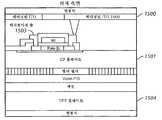
LCD를 제조하는 기본적인 프로세스 흐름(800)이 도 8에 도시되어 있다. 2개의 대형 마더 글라스의 시트들, 즉 LCD의 상부를 위한 시트와 하부를 위한 시트가 개별 처리 단계들(801 및 802)을 거친 후에 정렬되고(블록 803), 함께 압착되고, 가열되어(블록 804) 상부 및 하부 글라스 간의 시일(seal)들을 경화시킴으로써 안정된 패널 구조가 생성될 수 있다. 대형 패널은 그 후 스크라이브(scribe)되어 원하는 치수의 보다 작은 모듈들로 쪼개진다(블록 805). 개별 모듈들은 그들의 에지들이 그라인드(grind)된(블록 806) 후에 액정들로 충전된다(블록 807). 충전 후에, 모듈들은 실링(seal)될 수 있다(블록 808). 편광자들 및 전기 컴포넌트들이 부착될 수 있다(블록 809). 프로세스의 종료 시에 또는 종료 무렵에 연성 인쇄 회로(FPC)들이 그들의 기판들에 부착될 수 있다(블록 810).The
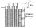
완성된 LCD 모듈(900)이 도 9에 도시되어 있다. 도시된 LCD 모듈은 하부 글라스(902)에 부착된 칩 온 글라스(COG) LCD 드라이버(901)를 포함하고 또한 하부 글라스(902)에 부착된 FOG(flex on glass) 연성 인쇄 회로(FPC)(903)를 포함한다. 양쪽 컴포넌트들은 ACA(anisotropic conductive adhesive)를 이용하여 하부 글라스 패드들에 전기적으로 접속되고 제자리에 유지될 수 있다. 하부 글라스(902)는 상부 글라스(904)를 넘어서 연장하여 COG LCD 드라이버(901), FPC(903), 및 기타 지지 컴포넌트들을 설치하기 위한 선반부(shelf)(905)를 제공할 수 있다. 핸드헬드 장치들의 경우, LCD에 대한 컨트롤들 및 데이터를 관리하는 시스템 프로세서 보드는 백라이트(906)의 아래에 배치될 수 있다.The completed
터치 감지를 지지하는 데 이용될 수 있는 추가의 컴포넌트들(예를 들면, FPC들)도 선반부(905)에 부착될 수 있다. 다른 부착 포인트들도 가능하다. 그 상세는 후술되는 관련 실시예들과 관련하여 논의된다.Additional components (eg, FPCs) that can be used to support touch sensing can also be attached to the
1.4.1.4.LCDLCD 및 터치 감지의 결합 And touch sensing
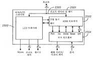
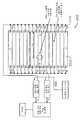
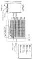
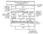
여기서 논의되는 스택업도들은 도 10 및 11의 블록도들과 관련하여 더 잘 이해될 수 있다. 위에서 시작하여, 터치 감지 전극들(1001, 1101)은 LCD 상부 글라스(1002, 1102)의 상부(사용자 측)에 적층될 수 있다. 터치 구동 전극들(1003, 1103)은 상부 글라스(1002, 1102)의 하부 측에 패터닝될 수 있다. 도전성 도트들(1004, 1104)은 구동 전극들(1003, 1103)을 드라이버(1005, 1105)에 접속할 수 있고, 드라이버(1005, 1105)는 또한 하부 글라스(1006, 1106) 상에 위치할 수 있다. 하부 글라스(1006, 1106) 상의 선반부(1007, 1107)는 LCD 드라이버 칩(1008, 1108) 및 터치 센서 드라이버 칩(1009)을 하우징할 수 있고, LCD 드라이버 칩과 터치 센서 드라이버 칩은 서로 인터페이스하거나(도 10) 단일 컴포넌트로 통합될 수 있다(도 11). 마지막으로, 또한 선반부에 접합된 FPC(1010, 1110)는 호스트 장치(1011, 1111)를 접속할 수 있다.The stackup diagrams discussed herein may be better understood with respect to the block diagrams of FIGS. 10 and 11. Starting from above, the
2.2.통합 옵션들Integration options
통합에 필수적인 터치 감지를 갖는 LCD의 일부 실시예들은 상부 글라스 및 하부 글라스를 포함할 수 있다. 이 2개의 글라스 층들 사이의 액정층을 통과하는 광의 양에 영향을 미치도록 디스플레이 제어 회로가 이들 글라스 층들 중 한쪽 및/또는 양쪽 모두에 형성될 수 있다. 상부 및 하부 글라스의 외부 에지들 사이의 공간을 여기서는 액정 모듈(LCM; liquid crystal module)이라고 부른다.Some embodiments of LCDs with touch sensing necessary for integration may include top glass and bottom glass. Display control circuitry may be formed in one and / or both of these glass layers to affect the amount of light passing through the liquid crystal layer between these two glass layers. The space between the outer edges of the upper and lower glass is referred to herein as a liquid crystal module (LCM).
전형적인 LCD 스택업(1200)은 도 12에서 도시된 바와 같이 전형적으로 추가의 층들을 포함한다. 도 12에서, 하드 코팅된(hard-coated) PMMA 층(1201)은 LCD 편광자(1202) 및 상부 글라스(1203)를 보호할 수 있고, 하부 글라스(1204)와 백라이트(1206) 사이에 제2 편광자(1205)가 포함될 수 있다.A
터치 감지 기술을 LCD에 통합하는 것은 다양한 기법들을 이용하여 달성될 수 있다. 예를 들면, 디스플레이 및/또는 제조 비용, 디스플레이 사이즈, 디스플레이 복잡성, 디스플레이 내구성, 디스플레이 기능성, 및 이미지 디스플레이 품질 등과 같은 인자들이 변화하는 상이한 실시예들에 있어서, 상이한 터치 감지 소자들 및/또는 층들이 LCD 디스플레이에 통합될 수 있다. 일부 실시예에서는, LCM의 외부의 LCD 디스플레이 상에 터치 감지 소자들을 통합함으로써 터치 감지 능력이 LCD에 포함될 수 있다. 다른 실시예에서는, 터치 감지 소자들이 LCM의 외부뿐 아니라 LCM의 내부(예를 들면, 2개의 글라스 층들 사이) 양쪽 모두에 추가될 수 있다. 또 다른 실시예에서는, 터치 감지 소자들의 세트가 LCM의 내부(예를 들면, 2개의 글라스 층들 사이)에만 추가될 수 있다. 다음의 섹션들은 위에서 언급한 실시예들 각각에 대한 다수의 컨셉트를 설명한다.Integrating touch sensing technology into an LCD can be accomplished using a variety of techniques. For example, in different embodiments where factors such as display and / or manufacturing cost, display size, display complexity, display durability, display functionality, and image display quality vary, different touch sensing elements and / or layers may be It can be integrated into the LCD display. In some embodiments, touch sensing capability may be included in the LCD by integrating touch sensing elements on an LCD display external to the LCM. In other embodiments, touch sensing elements may be added both inside the LCM as well as inside the LCM (eg, between two glass layers). In another embodiment, a set of touch sensing elements can be added only inside the LCM (eg, between two glass layers). The following sections describe a number of concepts for each of the above-mentioned embodiments.
2.1. 액정 모듈(2.1. LCD moduleLCMLCM)의 외부의 터치 감지Touch detection outside of
LCM의 외부에 터치 감지 소자들을 추가할 경우 전형적인 LCD 제조 관행에 거의 내지 전혀 영향을 미치지 않고 LCD 디스플레이에 터치 감지 능력이 추가될 수 있다. 예를 들면, 터치 감지 시스템 및 LCD 디스플레이 시스템은 개별적으로 제조되고 최종 단계에서 통합되어 터치 감지 능력을 갖는 LCD를 형성할 수 있다. LCD의 외부에 터치 감지 소자들을 포함시키는 경우는 또한 터치 감지 소자들이 사용자에 의해 터치되는 영역에 가까이 배치되도록 할 수 있어, 잠재적으로 디스플레이와 터치 컴포넌트들 사이의 전기적 간섭을 감소시킬 수 있다.Adding touch sensing elements outside the LCM can add touch sensing capability to the LCD display with little to no impact on typical LCD manufacturing practices. For example, the touch sensing system and the LCD display system can be manufactured separately and integrated in the final stage to form an LCD with touch sensing capability. Including touch sensing elements outside of the LCD can also allow the touch sensing elements to be placed close to the area touched by the user, potentially reducing electrical interference between the display and touch components.
컨셉트 C 및 컨셉트 N으로서 식별된 다응 2개의 실시예들은 그러한 외부의 터치 감지 소자들을 통합할 수 있다.The two embodiments identified as Concept C and Concept N may incorporate such external touch sensing elements.
2.1.1.2.1.1.컨셉트Concept C C
본 발명의 일 실시예인, 컨셉트 C는 LCD로부터 터치 기능이 분리되도록 하는 도 13에서 도시된 스택업을 이용한다. 컨셉트 C에서는, 2개의 추가의 인듐-주석 산화물(ITO) 층들(IT01(1301) 및 IT02(1302))이 컬러 필터(CF) 플레이트(예를 들면, 상부 글라스 층)의 위에 패터닝될 수 있다. 이들 층들은 터치 센서, 예를 들면, 상호 커패시턴스 터치 센서의 터치 감지 및 터치 구동 소자들을 위해 이용될 수 있다. 이들 ITO 층들은 (도 1 및 2에서 도시되고, 전술한 멀티 터치 감지 설명에서 설명된 바와 같이) 컬럼들 및/또는 로우들로 패터닝될 수 있고, 글라스 기판 또는 얇은(예를 들면, 5-12mm) SiO2 층과 같은 유전체(1305)에 의해 분리될 수 있다.Concept C, which is an embodiment of the present invention, utilizes the stackup shown in FIG. 13 to allow the touch function to be separated from the LCD. In Concept C, two additional indium-tin oxide (ITO) layers (
일부 실시예에서, 터치 소자들에서 사용되는 전극 패턴은 시각적 아티팩트(visual artifacts)를 감소시키도록 최적화될 수 있다. 예를 들면, 도 14는 시각적 아티팩트를 감소시킬 수 있는 마름모꼴 전극 패턴을 도시한다.In some embodiments, the electrode pattern used in the touch elements can be optimized to reduce visual artifacts. For example, FIG. 14 illustrates a rhombic electrode pattern that can reduce visual artifacts.
컨셉트 C에서는, 터치 감지 데이터를 운반하는 FPC들이 상부 글라스(1303)의 상부 표면에 부착될 수 있다.In Concept C, FPCs carrying touch sensitive data may be attached to the top surface of
2.1.2.2.1.2.컨셉트Concept N N
본 발명의 일 실시예인, 컨셉트 N은 자기 커패시턴스 감지를 이용하여 컬러 필터(CF) 플레이트의 외부 표면 상에 용량성 감지를 구현할 수 있다. 컨셉트 N은 터치 감지 컴포넌트들이 CF 플레이트(1501)(상부 글라스)의 위에 위치할 수 있는 도 15에서 도시된 스택업을 이용할 수 있다. 컨셉트 N에 기초한 LCD들은, 예를 들면, 종래의 TFT 플레이트(1504)에 대하여 이용되는 동일한 LTPS 프로세스를 이용하여 CF 플레이트(1501) 상에 패터닝된 ITO(1500) 및 2개의 금속층들을 갖는 TFT들(1503)을 형성함으로써 표준 LCD 프로세싱을 변경하지 않고 구성될 수 있다. 터치 ITO 층(1500)은 복수의 터치 픽셀들(1612)(도 16)로 패터닝될 수 있다. 터치 ITO 층(1500)은 사용자에 의해 터치되는 표면으로도 작용할 수 있는 플라스틱 커버(1702)(도 17에 도시됨)에 의해 보호될 수 있다.Concept N, which is an embodiment of the present invention, can implement capacitive sensing on the outer surface of the color filter (CF) plate using magnetic capacitance sensing. Concept N may use the stackup shown in FIG. 15 in which touch sensing components may be placed on top of CF plate 1501 (top glass). LCDs based on Concept N, for example, have TFTs with
도 16은 컨셉트 N에 대한 셀프 커패시턴스 터치 픽셀 회로를 도시한다. 각 ITO 터치 픽셀(1612)은 2개의 TFT, 예를 들면, 입력 TFT(1604) 및 출력 TFT(1608)에 접속될 수 있다. 입력 TFT(1604)는 ITO 터치 픽셀(1612)을 충전시킬 수 있고, 반면 출력 TFT(1608)는 ITO 터치 픽셀(1612)을 방전시킬 수 있다. 이동되는 전하의 양은 ITO 터치 픽셀(1602)의 커패시턴스에 좌우될 수 있고, 그 커패시턴스는 손가락의 근접에 의해 변경될 수 있다. 자기 커패시턴스 터치 감지의 추가 상세에 대해서는 위에서 및, 본원에 전체적으로 참고로 통합되는, 2001년 11월 27일에 발행된, "Method and Apparatus for Integrating Manual Input"이라는 명칭의, 미국 특허 6,232,846호에서 설명되어 있다.FIG. 16 shows a self capacitance touch pixel circuit for Concept N. FIG. Each
일 실시예에서는, 도 16 및 18에서 출력 컬럼(1610) 'CO' 및 출력 게이트들(1606) 'R3'에 대하여 도시된 바와 같이, 출력 컬럼(1610)은 수직으로 터치 픽셀들에 의해 공유될 수 있고, 출력 게이트들(1606)은 수평으로 터치 픽셀들에 의해 공유될 수 있다.In one embodiment, as shown for output column 1610 'CO' and output gates 1606 'R3' in FIGS. 16 and 18,
2.2. 부분적으로 통합된 터치 감지2.2. Partially integrated touch sensing
LCM의 내부에 터치 감지 소자들을 통합하는 것은 다양한 이점들을 제공할 수 있다. 예를 들면, LCM의 내부에 추가된 터치 감지 소자들은 디스플레이 기능을 위해서만 사용되었을 ITO 층들 또는 다른 구조들을 터치 감지 기능도 제공하도록 "재사용"할 수 있을 것이다. 기존의 디스플레이 층들에 터치 감지 특징들을 통합하는 것은 또한 층들의 총수를 감소시킬 수 있고, 이는 디스플레이의 두께를 감소시키고 제조 프로세스를 단순화할 수 있다.Integrating touch sensing elements inside the LCM can provide various advantages. For example, touch sensing elements added inside the LCM may "reuse" ITO layers or other structures that would only be used for display functionality to provide touch sensing as well. Integrating touch sensing features into existing display layers can also reduce the total number of layers, which can reduce the thickness of the display and simplify the manufacturing process.
다음의 실시예들은 LCM의 내부와 외부에 터치 감지 소자들을 포함할 수 있다. LCM 내에 터치 감지 소자들을 통합할 경우 2개의 기능들 간의 간섭 및 잡음이 생길 수 있기 때문에, 다음의 디자인들은 또한 둘 간의 전기적 간섭에 의해 야기되는 디스플레이 및/또는 터치 감지 출력들에 대한 부정적인 영향들을 감소시키거나 제거하면서 소자들이 공유되도록 하는 기법들을 포함할 수 있다.The following embodiments may include touch sensing elements inside and outside the LCM. Since incorporating touch sensing elements within the LCM can introduce interference and noise between the two functions, the following designs also reduce negative effects on the display and / or touch sensing outputs caused by electrical interference between the two. Techniques may be included to allow devices to be shared while making or removing them.
2.2.1.2.2.1.컨셉트Concept A A
컨셉트 A는, 상부 글라스와 편광자(2003) 사이에, 상부 글라스(2002)의 사용자 측에 배치된 멀티 터치 가능한("MT") ITO 감지층(IT01)(2001)을 갖는, 도 20에서 도시된 기본 스택업(2000)을 이용할 수 있다. 위로부터 시작하여, 터치 감지층들은: IT01(2001)(N개의 감지(또는 구동) 라인들로 패터닝될 수 있는 ITO 층) 및 IT02(2004)(M개의 감지(또는 구동) 라인들로 패터닝될 수 있는 ITO 층)를 포함할 수 있다. IT02 층(2004)은 또한 LCD에 대한 VCOM 전극으로도 작용할 수 있다.Concept A is shown in FIG. 20, having a multi-touchable (“MT”) ITO sensing layer (IT01) 2001 disposed between the top glass and the
2.2.1.1.2.2.1.1.컨셉트Concept A: 터치 센서 전극 A: touch sensor electrode
터치 센서 전극 어레이는 도 21(좌측)에 도시된 바와 같이 2개의 패터닝된 ITO 층들을 포함할 수 있다. 도 21은 터치 센서 전극들의 하나의 가능한 구현의 단순화된 도시이다. 관찰자(viewer)에게 더 가까이 있는 층인 IT01(2101)은 감지층 또는 감지 라인이라고도 불리는 터치 출력층일 수 있다. 터치 구동층(2102)은 IT02 층 상에 위치할 수 있다. IT02는 또한 커패시터 CLC(도 7 참조)의 상위 전극을 형성할 수 있다. 도 21(우측)은 또한 3개의 감지 픽셀들(2103a, 2103b, 및 2103c)와 함께 관련된 커패시터들의 상세를 보여준다. 감지 라인 및 구동 라인 양쪽 모두는 5 mm 피치 및 10 내지 30 마이크로미터 갭을 가질 수 있다. 이 갭은 육안으로는 보이지 않을 만큼 작을 수 있지만, 그럼에도 단순 근접 마스크(simple proximity mask)를 이용해 에칭하기에는 용이할 만큼 클 수 있다. (도면 내의 갭들은 크게 과장되어 있다.)The touch sensor electrode array can include two patterned ITO layers as shown in FIG. 21 (left). 21 is a simplified illustration of one possible implementation of touch sensor electrodes.
도 22는 케이블링 및 서브시스템 배치의 상면도(2201) 및 측면도(2202)를 갖는, 컨셉트 A에 대한 하나의 가능한 물리적 구현을 보여준다. 상면도(2201)는 접히지 않은 상태의 FPC(2203)(아래에서 더 상세히 논의됨)의 대략 위치들을 보여준다. 도 14는 단지 개별 터치 레벨 시프터/디코더 COG가 이용될 수 있는 하나의 물리적 구현을 나타낸다. 개별 터치 컴포넌트들의 수를 최소화하는 대안 아키텍처는 아래에서 논의된다. 기계적 안정성을 위하여, FPC는 측면도(2202)에서 도시된 바와 같이 구부려질 수 있고, 그에 따라 T-탭(2204) 및 B-탭(2205) 본드들에 대한 응력이 최소화된다. 도 23은 주요 하부 글라스 컴포넌트들의 하나의 가능한 아키텍처(2300), 및 터치 감지를 위해 이용되는 상부 글라스 상의 분할된 IT02 층(2301)을 보여주는 고레벨 블록도이다. 상부 글라스 상의 IT02의 세그먼트들(2302)은 각각 도전성 도트(2303)를 하부 글라스 상의 대응하는 패드에 접속한다. 하부 글라스 상의 패드들은 각각 아래에서 논의되는 터치 드라이버에 접속할 수 있다.22 shows one possible physical implementation for Concept A, with a
2.2.1.22.2.1.2컨셉트Concept A: 도전성 A: conductive도트dot
LCD의 코너들에 위치하는 도전성 도트들은 VCOM 전극을 구동 회로들에 접속하는 데 이용될 수 있다. 터치 구동 라인들을 터치 구동 회로에 접속하기 위해 추가의 도전성 도트들이 이용될 수 있다. 도트들은 터치 구동 신호들(아래에서 더 상세히 논의됨)의 위상 지연에 현저하게 추가하지 않도록 충분히 낮은 저항을 가질 수 있다. 이것은 도전성 도트들의 저항을 10 옴 이하로 제한하는 것을 포함할 수 있다. 요구되는 리얼 에스테이트(real estate)를 감소시키기 위해 도전성 도트들의 사이즈도 제한될 수 있다.Conductive dots located at the corners of the LCD can be used to connect the VCOM electrode to the drive circuits. Additional conductive dots can be used to connect the touch drive lines to the touch drive circuit. The dots may have a resistance low enough to not add significantly to the phase delay of the touch drive signals (discussed in more detail below). This may include limiting the resistance of the conductive dots to 10 ohms or less. The size of the conductive dots may also be limited in order to reduce the required real estate.
도 24에서 도시된 바와 같이, 신장된 도전성 도트들(2401)은 도트 저항 및 리얼 에스테이트 양쪽 모두의 요건들을 감소시키기 위해 이용될 수 있다. 터치 구동 세그먼트들(2402)은 폭이 약 5 mm일 수 있고, 이는 도트 저항을 감소시키는 큰 면적을 제공할 수 있다.As shown in FIG. 24, stretched
2.2.1.3.2.2.1.3.컨셉트Concept A: 연성 회로 및 터치/ A: flexible circuit and touch /LCDLCD 드라이버 driverICIC
종래의 디스플레이(예를 들면, 도 9)는 디스플레이의 저레벨 동작을 제어할 수 있는 LCD 드라이버 회로(IC)(901)를 가질 수 있다. 시스템 호스트 프로세서는 명령 및 디스플레이 데이터를 LCD 드라이버(901)에 보냄으로써 디스플레이에 대하여 고레벨 제어를 행사할 수 있다. 멀티 터치 시스템들은 또한 하나 이상의 드라이버 IC들을 가질 수 있다. 통합된 참고 문헌들에서 설명된, 하나의 예시적인 멀티 터치 가능한 시스템은 3개의 IC, 즉, 멀티 터치 컨트롤러, 외부 레벨-시프터/디코더, 및 ARM 프로세서와 같은 컨트롤러를 포함한다. ARM 프로세서는 멀티 터치 컨트롤러에 대하여 저레벨 제어를 행사할 수 있고, 후자는 그 후 레벨-시프터/디코더를 제어할 수 있다. 시스템 호스트 프로세서는 ARM 프로세서에 대하여 고레벨 제어를 행사할 수 있고 그로부터 터치 데이터를 수신할 수 있다. 일부 실시예에서, 이들 드라이버들은 단일 IC로 통합된다.A conventional display (eg, FIG. 9) may have an LCD driver circuit (IC) 901 that can control the low level operation of the display. The system host processor may exercise high level control over the display by sending commands and display data to the
도 25는 터치/LCD 드라이버 통합 회로(2501)에 대한 예시적인 고레벨 블록도를 도시한다. 이 IC는 2가지 주요 기능, 즉, 1) LCD 제어 및 업데이트, 및 2) 터치 스캐닝 및 데이터 처리의 기능을 갖고 있다. 이들 2가지 기능들은 LCD 제어를 위한 LCD 드라이버 부분(2502) 및 터치 스캐닝 및 처리를 위한 ARM 프로세서(2503) 및 멀티 터치 컨트롤러(2504)에 의해 통합될 수 있다. 터치 회로들은 어느 하나가 다른 하나를 방해하지 못하도록 LCD 스캐닝과 동기화될 수 있다. 호스트와, LCD 드라이버 또는 ARM 프로세서 간의 통신은 호스트 데이터 및 제어 버스(2505)를 통하여 이루어질 수 있다. 더 완전히 통합된 터치/LCD 드라이버에 대해서는 아래에서 논의된다.25 shows an exemplary high level block diagram for touch / LCD driver integrated
도 26에서 도시된 바와 같이, 다양한 터치 및 디스플레이 층들에 대한 신호들을 불러 모으는 FPC(2601)는 3개의 커넥터 탭, 즉, T-탭(2602), B-탭(2603), 및 호스트 탭(2604)을 가질 수 있다. T-탭은 상부 글라스 상의 감지 라인 패드들에 접속할 수 있다. T-탭 트레이스들(2605)은 B-탭(2603) 상의 대응하는 패드들에 접속할 수 있고, B-탭은 또한 하부 글라스 상에 부착될 수 있다. B-탭(2603)은 또한 호스트가 터치/LCD 드라이버 IC에 접속하게 할 수 있는 호스트 탭(2604)으로부터의 통과 루트들(pass-through routes)(2606)을 제공할 수 있다. FPC(2601)는 또한 터치 및 LCD 동작을 지원하는 다양한 컴포넌트들(2607)에 대한 기판을 제공할 수 있고, 또한 2개의 패드들(2608)을 통하여 백라이트 FPC에 접속할 수 있다.As shown in FIG. 26, the
FPC(2601)는 상부 및 하부 글라스 양쪽 모두에 접합된 TAB일 수 있다. 대안적으로는, 다른 접합 방법들이 이용될 수 있다.
2.2.1.4.2.2.1.4.컨셉트Concept A: 하부 글라스 상에 통합된 터치 구동 A: touch drive integrated on the bottom glass
레벨 시프터/디코더 칩은, 개별 전압 승압기(voltage booster)(예를 들면 3V 대 18V 승압기)와 함께, 터치 감지를 위한 고전압 구동 회로를 제공할 수 있다. 일 실시예에서, 터치/LCD 드라이버 IC는 레벨 시프터/디코더 칩을 제어할 수 있다. 대안적으로, 전압 승압기 및/또는 레벨 시프터/디코더는 터치/LCD 드라이버 IC에 통합될 수 있다. 예를 들면, 그러한 통합은 고전압(18Y) LTPS 프로세스를 이용하여 실현될 수 있다. 이는 레벨 시프터/디코더 칩 및 전압 승압기를 하부 글라스의 주변부에 통합하는 것을 가능하게 할 수 있다. 레벨 시프터/디코더는 또한 아래에서 논의되는 바와 같이 VCOM 변조 및 터치 구동을 위한 전압들을 제공할 수 있다.The level shifter / decoder chip, together with a separate voltage booster (eg 3V to 18V booster), can provide a high voltage drive circuit for touch sensing. In one embodiment, the touch / LCD driver IC can control the level shifter / decoder chip. Alternatively, the voltage booster and / or level shifter / decoder may be integrated into the touch / LCD driver IC. For example, such integration can be realized using a high voltage 18Y LTPS process. This may make it possible to integrate the level shifter / decoder chip and the voltage booster at the periphery of the bottom glass. The level shifter / decoder may also provide voltages for VCOM modulation and touch drive as discussed below.
2.2.1.5.2.2.1.5.컨셉트Concept A: A:LCDLCDVVCOMCOM과의 터치 구동 공유Touch-driven sharing with
위에서 논의된 바와 같이, 컨셉트 A는 터치 감지 라인들로서 기능할 수 있는, 하나의 ITO 층을 표준 LCD 스택업에 추가할 수 있다. 터치 구동층은 IT02로도 표시된, LCD의 VCOM 평면과 공유될 수 있다. 디스플레이 동작을 위해서는, 표준 비디오 리프레시 레이트(예를 들면, 60 fps)가 이용될 수 있다. 터치 감지를 위해서는, 적어도 초당 120회의 레이트가 이용될 수 있다. 그러나, 터치 스캐닝 레이트는 또한 디스플레이 리프레시 레이트와 일치할 수 있는 초당 60 스캔과 같은 보다 느린 레이트로 감소될 수도 있다. 일부 실시예에서는, 디스플레이 리프레시 또는 터치 스캐닝의 어느 쪽도 중단(interrupt)하지 않는 것이 바람직할 수 있다. 그러므로, (동일한 또는 상이한 레이트에서 일어나고 있을 수 있는) 디스플레이 리프레시 또는 터치 스캐닝을 감속하거나 중단하는 일 없이 IT02 층의 공유를 허용할 수 있는 방식에 대하여 이제 설명한다.As discussed above, Concept A can add one ITO layer to the standard LCD stackup, which can function as touch sense lines. The touch drive layer can be shared with the VCOM plane of the LCD, also denoted IT02. For display operation, a standard video refresh rate (eg, 60 fps) can be used. For touch sensing, a rate of at least 120 times per second may be used. However, the touch scanning rate may also be reduced to a slower rate, such as 60 scans per second, which may match the display refresh rate. In some embodiments, it may be desirable not to interrupt either display refresh or touch scanning. Therefore, a description is now given of the manner in which sharing of the IT02 layer can be allowed without slowing down or interrupting display refresh or touch scanning (which may be happening at the same or different rates).
도 27에는 동시의 디스플레이 업데이트 및 터치 스캐닝이 도시되어 있다. 이 예에서는, 5개의 멀티 터치 구동 세그먼트들(2700, 2701, 2702, 2703, 2704)이 도시되어 있다. 각 터치 구동 세그먼트는 M개의 디스플레이 로우들과 겹칠 수 있다. 디스플레이는 초당 60 프레임으로 스캔될 수 있는 반면 멀티 터치 센서 어레이는 초당 120회 스캔될 수 있다. 도면은 하나의 디스플레이 프레임의 시간 전개(time evolution)가 16.67 msec 지속하는 것을 보여준다. 현재 업데이트되고 있는 디스플레이의 영역은 바람직하게는 능동 터치 구동 세그먼트와 겹치지 않아야 한다.27 shows simultaneous display update and touch scanning. In this example, five
패치(2705)는 디스플레이 로우들이 어디서 업데이트되고 있는지를 나타낸다. 패치(2706)는 능동 터치 구동 세그먼트를 나타낸다. 도 27의 상좌측 코너에서, 디스플레이 프레임의 시작에서는 첫 번째 M/2개 디스플레이 라인들이 리프레시될 수 있다. 동시에, 터치 감지를 위하여 터치 구동 세그먼트 1(2701)이 구동될 수 있다. 도면의 우측으로 이동하여, 시간 t=1.67ms에서, 다음 그림은 다음 M/2개 디스플레이 로우들이 리프레시되고 있고, 동시에 터치 구동 세그먼트 2(2702)가 구동될 수 있음을 보여준다. 이 패턴의 약 8.3 msec 후에는, (제2 로우의 시작) 각 터치 구동 세그먼트가 1회 구동되었을 수 있고, 디스플레이의 1/2이 리프레시되었을 것이다. 다음 8.3 msec에서는, 전체 터치 어레이가 다시 스캔될 수 있고, 따라서 120 fps의 스캐닝 레이트를 제공하는 한편, 디스플레이의 나머지 1/2이 업데이트된다.
디스플레이 스캐닝은 전형적으로 라인 순서대로 진행하기 때문에, 터치 구동 세그먼트들은 디스플레이 및 터치 활동의 겹침을 방지하기 위해 순차적인 순서에 어긋나게 구동될 수 있다. 도 27에 도시된 예에서는, 터치 구동 순서는 첫 번째 8.3 msec 동안에는 1,2,3,4,0이었고, 두 번째 8.3 msec 기간에는 1,2,4,3,0이었다. 실제 순서는 터치 구동 세그먼트들의 수 및 디스플레이 로우들의 수에 따라서 변화할 수 있다. 그러므로, 일반적으로, 터치 구동 사용의 순서를 프로그램하는 능력은 바람직할 수 있다. 그러나, 어떤 특수한 경우들에 있어서는, 고정된 시퀀스 순서로 충분할 수 있다.Since display scanning typically proceeds in line order, touch drive segments can be driven out of sequential order to prevent overlap of display and touch activity. In the example shown in FIG. 27, the touch driving sequence was 1,2,3,4,0 during the first 8.3 msec and 1,2,4,3,0 during the second 8.3 msec period. The actual order may vary depending on the number of touch drive segments and the number of display rows. Therefore, in general, the ability to program the order of touch drive use may be desirable. However, in some special cases, a fixed sequence order may be sufficient.
업데이트되고 있는 디스플레이의 영역으로부터 더 멀리 떨어져서 능동 터치 구동 세그먼트를 분리하는 것이 바람직할 수도 있다(이미지 품질 이유로). 이것은 도 27에서 도시되어 있지 않지만, 충분한 개수의 터치 구동 세그먼트들(예를 들면, 6개 이상의 세그먼트들)이 주어지면 용이하게 행해질 수 있다.It may be desirable to separate the active touch drive segment further away from the area of the display being updated (for image quality reasons). This is not shown in FIG. 27, but can be easily done given a sufficient number of touch drive segments (eg, six or more segments).
그러한 기법들은 고주파 디스플레이 구동 소자를 지원하는 다중화(multiplex) 회로를 요구하지 않고 디스플레이 및 터치 감지 소자들에 대한 상이한 리프레시 레이트들을 효과적으로 가능하게 할 수 있다.Such techniques can effectively enable different refresh rates for display and touch sensing elements without requiring multiplexing circuitry to support high frequency display driving elements.
2.2.1.6.2.2.1.6.컨셉트Concept A: A:VVCSTCST 구동 옵션들 Drive options
도 6에서 도시된 바와 같이, VCST 및 VCOM은 함께 접속될 수 있고 따라서 LC를 가로질러 원하는 AC 파형을 달성하도록 함께 변조될 수 있다. 이것은 VCOM 변조를 이용할 때 적당한 디스플레이 리프레시를 달성하는 데 도움을 줄 수 있다. VCOM이 터치 구동을 위하여 이용되는 경우, VCST도 변조할 필요는 없다. 이것은 후술되는 개회로 VCST 옵션으로서 간주될 수 있다. 그러나, VCST가 VSTM으로 변조되면, 터치 구동 신호 VSTM 상의 용량성 부하가 감소될 수 있고, 이는 터치 신호의 보다 작은 위상 지연을 초래할 수 있다. 이것은 후술되는 구동 VCST 옵션으로서 간주될 수 있다.As shown in FIG. 6, VCST and VCOM may be connected together and thus modulated together to achieve the desired AC waveform across the LC. This can help to achieve adequate display refresh when using VCOM modulation. If VCOM is used for touch driving, then VCST also need not be modulated. This can be considered as the open circuit VCST option described below. However, if the VCST is modulated by VSTM, the touch drive signal may be a capacitive load on the VSTM reduced, which may result in the touch signal more small phase delay. This can be considered as the drive VCST option described below.
도 28은 개회로 VCST 옵션을 도시한다. 하부 도면(2802)은 하나의 터치 구동 세그먼트(2803)가 어떻게 M개의 디스플레이 로우들(2804)와 겹칠 수 있는지를 도시한다. 상부 글라스 상에 위치하는 터치 구동 세그먼트들(2803)은 도전성 도트(2805)를 통하여 하부 글라스 상의 회로들에 전기적으로 접속할 수 있다. 터치 구동 세그먼트 아래의 M개의 로우의 M개의 VCST 라인들이 디스플레이(2806)의 에지 상에서 함께 접속할 수 있다. 상부 도면(2801)은 그의 개별 저장 커패시터 CST를 갖는 서브픽셀에 대한 기본 회로를 보여준다. 상부 도면 내의 영역(2807)은 단일 터치 구동 세그먼트에 의해 커버되는 서브픽셀들의 M개의 인접한 로우들을 나타낼 수 있다. 특정 터치 구동/디스플레이 그룹에 대한 디스플레이 동작 및 터치 감지는 위에서 논의된 바와 같이 상이한 시간들에서 일어날 수 있다. 디스플레이 드라이버가 M개의 로우들 내의 서브픽셀들의 상태를 설정할 준비가 되면, 스위치들(2808, 2809)은 VCOMDrive(2810)를 M개의 VCST 라인들(2804)에 및 터치 구동 세그먼트(VCOM)에 접속할 수 있다. VCOMDrive 전압은 LCD 드라이버에 의해, 반전의 위상에 따라서, 접지 전압 또는 공급 전압 레일로 설정될 수 있다. 나중에, 이 터치 구동/디스플레이 그룹이 터치 사용을 위해 이용 가능하게 되면, 스위치들(2808, 2809)은 터치 구동 세그먼트를 VSTM(2811)에 접속하고 VCST를 VCOMDrive에서 분리하여, 그것을 개회로 상태(open state)로 되게 할 수 있다.28 shows the open circuit VCST option.
도 29는 구동-VCST 옵션을 도시한다. 하부 도면(2902)은 하나의 터치 구동 세그먼트(2903)가 어떻게 M개의 디스플레이 로우들(2904)과 겹칠 수 있는지를 도시한다. 상부 글라스 상에 위치하는 터치 구동 세그먼트들(2903)은 도전성 도트(2905)를 통하여 하부 글라스 상의 회로들에 전기적으로 접속할 수 있다. 특정 터치 구동 세그먼트 아래의 로우들의 M개의 VCST 라인들은 디스플레이(2906)의 에지 상에서 함께 접속할 수 있다. 상부 도면(2901)은 개별 저장 커패시터 CST를 갖는 서브픽셀에 대한 기본 회로를 보여준다. 상부 도면 내의 영역(2907)은 단일 터치 구동 세그먼트에 의해 커버되는 서브픽셀들의 M개의 인접한 로우들을 나타낼 수 있다. 디스플레이 동작 및 터치 감지는 상이한 시간들에서 일어날 수 있다. 디스플레이 드라이버가 M개의 로우들 내의 서브픽셀들의 상태를 설정할 준비가 되면, 스위치(2908)는 VCOMDrive(2910)를 M개의 VCST 라인들(2904)에 및 터치 구동 세그먼트(VCOM)에 접속할 수 있다. VCOMDrive 전압(2910)은 LCD 드라이버에 의해, 반전의 위상에 따라서, 전형적으로 접지 전압 또는 공급 전압 레일로 설정될 수 있다. 나중에, 이 터치 구동/디스플레이 그룹이 터치 사용을 위해 이용 가능하게 되면, 스위치(2908)는 VCST 및 터치 구동 세그먼트(VCOM)를 VSTM(2911)에 접속할 수 있다.29 shows the Drive-VCST option.
2.2.1.7.2.2.1.7.컨셉트Concept A: A:MTMT-구동-Driving용량성Capacitive 부하 Load
컨셉트 A의 터치 구동 라인 상의 용량성 부하는, 예를 들면, 픽셀 ITO 및 금속 루트들의 망(mesh)에 의해 커버될 수 있는 하부 글라스와 터치 구동층 간의 얇은(예를 들면, ~4 ㎛) 갭 때문에, 높을 수 있다. 액정들은 다소 높은 최대 유전 상수(예를 들면, 약 10)를 가질 수 있다.The capacitive load on the touch drive line of Concept A, for example, is a thin (eg, ~ 4 μm) gap between the bottom drive and the touch drive layer which may be covered by a mesh of pixel ITO and metal routes. Because of that, it can be high. Liquid crystals may have a somewhat higher maximum dielectric constant (eg, about 10).
터치 구동 세그먼트의 커패시턴스는 자극하는 터치 펄스 VSTM의 위상 지연에 영향을 미칠 수 있다. 만일 커패시턴스가 너무 높고, 따라서 너무 많은 위상 지연이 있다면, 결과의 터치 신호는 부정적으로 영향을 받을 수 있다. 본 발명자들에 의해 수행된 분석에 따르면 IT02 시트 저항을 약 30 Ω/sq 이하로 유지하면 위상 지연을 최적의 한계 내에 유지할 수 있다.The capacitance of the touch drive segment can affect the phase delay of the stimulating touch pulse VSTM . If the capacitance is too high and therefore there is too much phase delay, the resulting touch signal can be negatively affected. Analysis conducted by the inventors shows that keeping the IT02 sheet resistance below about 30 Ω / sq allows the phase delay to be within optimal limits.
2.2.1.8.2.2.1.8.컨셉트Concept A: 전기적 모델 및 A: electrical model andVVCOMCOM 유도 잡음 Induced noise
IT02는 터치 구동 및 LCD VCOM 양쪽 모두에 대하여 동시에 이용될 수 있기 때문에, VCOM의 변조는 터치 신호에 잡음을 추가할 수 있다.Since IT02 can be used simultaneously for both touch drive and LCD VCOM , modulation of VCOM can add noise to the touch signal.
예를 들면, 다른 터치 구동 세그먼트가 터치 감지를 위해 이용되고 있는 것과 동시에 하나의 터치 구동 세그먼트가 VCOM으로 변조되고 있는 경우 터치 신호에 잡음 성분이 추가될 수 있다. 추가되는 잡음의 양은 VSTM에 대한 VCOM 변조의 위상, 진폭, 및 주파수에 좌우된다. VCOM의 진폭 및 주파수는 LCD에 대하여 이용되는 반전 방법에 좌우된다.For example, a noise component may be added to the touch signal when one touch drive segment is being modulated to VCOM while another touch drive segment is being used for touch sensing. The amount of noise added depends on the phase, amplitude, and frequency of the VCOM modulation for VSTM . The amplitude and frequency of VCOM depends on the inversion method used for the LCD.
도 30은 터치 감지 및 LCD VCOM 변조 양쪽 모두를 위해 터치 구동이 이용되는 상황에 대한 전기적 모델을 도시한다. 이 모델은 VCOM 변조가 전하 증폭기(3002)의 입력에 잡음을 추가할 수 있는 입력 경로를 보여준다.30 shows an electrical model for the situation where touch drive is used for both touch sensing and LCD VCOM modulation. This model shows an input path through which VCOM modulation can add noise to the input of
일부 실시예에서, 전하 증폭기(3002)는 VCOM(3003)에 의해 유도되는 잡음을 수용할 추가의 공간(headroom)을 필요로 할 수 있다. 또한, 후속 필터링 회로들(예를 들면, 도시되지 않은 동기식 복조기)은 VCOM 변조로 인한 잡음 신호를 제거할 필요가 있을 수 있다.In some embodiments, the
2.2.1.9.2.2.1.9.컨셉트Concept A: A:VVSTMSTM 효과 effect
VSTM 변조는, 소정의 조건 하에서, 변조되고 있는 터치 구동 세그먼트 아래의 서브픽셀들의 전압에 부정적인 영향을 미칠 수 있다. 만일 서브픽셀 RMS 전압이 감지할 수 있을 정도로 변화하면, 디스플레이 아티팩트들이 생성될 수 있다. 결과로 생길 수 있는 디스플레이 일그러짐(display distortion)을 최소화하기 위해 다음의 기법들 중 하나 이상의 채용될 수 있다.VSTM modulation can negatively affect the voltage of the subpixels under the touch drive segment being modulated under certain conditions. If the subpixel RMS voltage changes noticeably, display artifacts can be generated. One or more of the following techniques may be employed to minimize the resulting display distortion.
2개의 측면으로부터의 터치 구동은 LC 픽셀 전압의 일그러짐을 감소시킬 수 있다. 도 31에서 도시된 바와 같이, 양쪽으로부터의 터치 구동은 VSTM을 도전성 도트들(3102)을 통하여 양쪽에 있는 CST 라인들에 접속함으로써 하부 글라스 상의 기존의 저저항 CST 루트들(3101)을 채용함으로써 달성될 수 있다. 대안적으로, 단일 종단형(single-ended) 터치 구동은 모든 픽셀들에 대하여 균일한 픽셀 오프셋 전압을 생성할 수 있고, 이는 데이터 구동 레벨들을 조절함으로써 감소되거나 제거될 수 있다. 또한, ITO 시트 저항을 감소시키는 것은 디스플레이 아티팩트들을 감소시키는 데 도움을 줄 수 있다. 마지막으로, 터치 신호 내의 잡음의 양을 감소시키기 위해 VSTM의 위상 및 주파수를 VCOM의 위상 및 주파수에 결합할 수도 있다.Touch driving from two sides can reduce the distortion of the LC pixel voltage. As shown in FIG. 31, touch drive from both sides connects the existing VSTM to CST lines on both sides via conductive dots 3102 to connect existing low resistance CST routes 3101 on the bottom glass. It can be achieved by employing. Alternatively, single-ended touch drive can generate a uniform pixel offset voltage for all pixels, which can be reduced or eliminated by adjusting the data drive levels. In addition, reducing the ITO sheet resistance can help to reduce display artifacts. Finally, the phase and frequency of VSTM may be combined with the phase and frequency of VCOM to reduce the amount of noise in the touch signal.
2.2.1.10.2.2.1.10.컨셉트Concept A: 제조에의 영향 A: Influence on Manufacturing
컨셉트 A에 대한 제조 프로세스는 전형적인 LCD 제조 프로세스에 관하여 추가의 단계들을 포함할 수 있다. 일부는 완전히 새로운 단계들일 수 있고 일부는 기존의 단계들에 대한 변형들일 수 있다. 도 32는 컨셉트 A에 대한 제조 프로세스 흐름을 도시한다. 블록들 3201, 3202, 및 3204는 새로운 단계들을 나타내고, 블록들 3205, 3206, 및 3207은 변경된 단계를 나타내고, 양쪽 모두 종래의 LCD 제조 프로세스들(예를 들면, 도 8의 것)에 관계가 있다.The manufacturing process for Concept A may include additional steps with respect to a typical LCD manufacturing process. Some may be entirely new steps and some may be variations on existing steps. 32 shows a manufacturing process flow for Concept A. FIG.
IT01을 적용 및 패터닝하는 것(블록 3201, 3202)은 공지된 방법들을 이용하여 행해질 수 있다. ITO는 LCD프로세싱의 나머지 동안에 보호될 수 있다. 제거 가능한 보호 코팅을 제공하기 위해 포토레지스터가 이용될 수 있다. 대안적으로, 실리콘 이산화물이 영구적인 보호 피복을 제공할 수 있다. IT02를 적응 및 패터닝하여(블록 3204) 유사한 방식으로 터치 구동 세그먼트들을 형성할 수 있다.Applying and patterning IT01 (
위상 지연의 분석에 따르면 IT01 및 IT02의 시트 저항은, 어느 한쪽 평면 상의 용량성 부하가 작다는 것을 조건으로, 소형 디스플레이(<= 4" 대각선)에 대하여 400 Ω/sq 정도로 높을 수 있다. 위에서 논의된 바와 같이, 컨셉트 A에 있어서의 용량성 부하는 IT02에 대한 최대 시트 저항을 약 30 Ω/sq 이하로 제한하는 것이 바람직할 수 있는 정도의 크기의 것일 수 있다.Analysis of the phase delay shows that the sheet resistance of IT01 and IT02 can be as high as 400 Ω / sq for small displays (<= 4 ”diagonal), provided that the capacitive load on either plane is small. As noted, the capacitive load in Concept A may be of such magnitude that it may be desirable to limit the maximum sheet resistance to IT02 to about 30 Ω / sq or less.
2.2.2.2.2.2.컨셉트Concept A60 A60
컨셉트 A60은 물리적으로 컨셉트 A와 유사할 수 있고 디스플레이 업데이트 및 터치 스캐닝을 동기화시키는 문제에 대해 상이한 접근법을 제공할 수 있다. 이것은 터치 신호(즉, VSTM)에 대한 자극으로서 VCOM의 1-라인 반전을 이용하는 것에 의해 달성될 수 있다. 이는 도 33에 도시되어 있고, 도 33은 다른 터치 세그먼트들은 일정한 전압에 유지될 수 있는 동안에 하나의 터치 구동 세그먼트(3301)가 어떻게 변조될 수 있는지를 보여준다. 이러한 접근법에 의하면, 터치 신호로부터 불필요한 VCOM 유도 전압을 제거하는 문제가 제거될 수 있다. 더욱이, 디스플레이 업데이팅 및 터치 센서 스캐닝을 공간적으로 분리할 필요가 없다. 그러나, 이 접근법을 이용하면, 본원에 참고로 통합된, 2006년 5월 2일에 출원된, "Multipoint Touch Screen Controller"라는 명칭의, 미국 특허 출원 11/381,313에서 설명된 다중 주파수 변조와는 대조적으로 단일 주파수(즉, VCOM 변조 주파수, 예를 들면, ~14.4 kHz)에서 복조가 햄해질 수 있다. 더욱이, 이 접근법을 이용하면, 터치 센서 스캔 레이트가 비디오 리프레시 레이트(예를 들면 초당 60)에 고정될 수 있다.Concept A60 may be physically similar to Concept A and may provide a different approach to the problem of synchronizing display updates and touch scanning. This can be accomplished by using 1-line inversion of VCOM as a stimulus to the touch signal (ie VSTM ). This is illustrated in FIG. 33, which shows how one
2.2.32.2.3컨셉트Concept B B
도 34에서 도시된 컨셉트 B는 컨셉트 A와 유사하여, 다수의 동일한 전기적, 케이블링, 및 구조적 양태들을 공유할 수 있다. 그러나, 컨셉트 B는 터치 구동층을 VCOM 층에 통합할 수 있다. 그러므로 컨셉트 B는 LCD 및 터치 감지를 위해 이용되는 ITO 층들의 개수 및 스택 위치가 상이할 수 있다. 유사점들 때문에, 이제 컨셉트 A와 컨셉트 B 간의 차이점들을 강조하여 컨셉트 B에 대하여 설명한다.Concept B shown in FIG. 34 is similar to Concept A, and may share many of the same electrical, cabling, and structural aspects. However, Concept B can integrate the touch drive layer into the VCOM layer. Concept B may therefore differ in the number and stack position of the ITO layers used for LCD and touch sensing. Because of the similarities, Concept B will now be described highlighting the differences between Concept A and Concept B.
컨셉트 B는 컨셉트 A의 공유된 IT02 층을 2개의 ITO 층들로 분할하여, 하나의 층은 터치 감지(IT02)(3402)를 위해 이용하고 하나의 층은 LCD VCOM(IT03)(3403)을 위해 이용할 수 있다. 위로부터 시작하여, 터치 감지를 위해 사용되는 층들은: N개의 터치 감지 라인들로 패터닝될 수 있는 ITO 층인, IT01(3401); M개의 터치 감지 라인들로 패터닝될 수 있는 ITO 층인, IT02(3402); 및 LCD에 대한 VCOM 전극으로서 작용할 수 있는 ITO 층인, IT03(3403)을 포함할 수 있다. 터치 구동층(IT02)(3402)은 상부 글라스(3404)의 하위 표면 상에, 컬러 필터(3405) 위에 적층될 수 있다.Concept B splits Concept A's shared IT02 layer into two ITO layers, one layer for touch sensing (IT02) 3402 and one layer for LCD VCOM (IT03) 3403. It is available. Starting from above, the layers used for touch sensing are:
터치 구동 소자들로부터 VCOM을 분리하는 것은 간섭을 감소시킬 수 있다.Separating VCOM from the touch drive elements can reduce interference.
2.2.3.1.2.2.3.1.컨셉트Concept B: 터치 센서 전극들 B: touch sensor electrodes
컨셉트 B는 컨셉트 A에 대하여 위에서 설명된 것들과 실질적으로 유사한 터치 센서 전극들을 포함할 수 있다.Concept B may include touch sensor electrodes that are substantially similar to those described above for Concept A.
2.2.3.2.2.2.3.2.컨셉트Concept B: 도전성 B: conductivity도트들Dots
컨셉트 A에서와 같이, 컨셉트 B는 터치 구동 세그먼트들을 전용 회로에 접속하기 위해, LCD의 코너들에 위치할 수 있는, 추가의 도전성 도트들(3406)을 이용할 수 있다. VCOM은 터치 감지와 공유될 필요가 없기 때문에, 컨셉트 B는 VCOM을 그의 구동 회로에 접속하는 코너 도트들을 유지할 수 있다. 또한(아래에서 논의되는 바와 같이), 컨셉트 B는 VCOM에 대하여 한층 더 많은 도전성 도트들을 추가할 수 있다.As in Concept A, Concept B may use additional
2.2.3.3.2.2.3.3.컨셉트Concept B: 연성 회로 및 터치/ B: flexible circuit and touch /LCDLCD 드라이버 driverICIC
컨셉트 B는 컨셉트 A에 대하여 설명된 것들과 실질적으로 유사한 FPC 및 터치/LCD 드라이버 IC를 이용할 수 있다.Concept B may use an FPC and touch / LCD driver IC substantially similar to those described for Concept A.
2.2.3.4.2.2.3.4.컨셉트Concept B: B:LCDLCD 스캐닝과의 동기화 Synchronization with Scanning
컨셉트 B에 있어서는, 비록 VCOM 층이 터치 구동층과 분리될 수 있지만, 그럼에도 업데이트되고 있는 디스플레이 영역으로부터 능동 터치 구동을 물리적으로 분리하기 위해 터치 스캐닝을 LCD 업데이팅과 동기화하는 것이 바람직할 수 있다. 컨셉트 A에 대하여 이전에 설명된 동기화 방식들은 컨셉트 B에 대해서도 이용될 수 있다.For Concept B, although the VCOM layer may be separate from the touch drive layer, it may nevertheless be desirable to synchronize touch scanning with LCD updating to physically separate the active touch drive from the display area being updated. The synchronization schemes previously described for Concept A may be used for Concept B as well.
2.2.3.52.2.3.5컨셉트Concept B: B:MTMT-구동-Driving용량성Capacitive 부하 Load
컨셉트 A와 마찬가지로, 컨셉트 B의 터치 구동 라인 상의 용량성 부하는 높을 수 있다. 터치 구동(IT02)(3402)과 VCOM 평면(IT03)(3403) 사이의 얇은(예를 들면, ~5 ㎛) 유전체로 인해 큰 커패시턴스가 있을 수 있다. 터치 자극 신호에서 바람직하지 못한 위상 지연을 감소시키는 한 가지 방법은 평행 금속 트레이스들의 추가를 통하여 ITO 구동 라인 저항을 저하시키는 것을 수 있다. 위상 지연은 레벨 시프터/디코더의 출력 저항을 감소시키는 것에 의해서도 감소될 수 있다.As with Concept A, the capacitive load on Concept B's touch drive line can be high. There may be large capacitance due to the thin (eg, ˜5 μm) dielectric between the touch drive (IT02) 3402 and the VCOM plane (IT03) 3403. One way to reduce undesirable phase delay in the touch stimulus signal may be to lower the ITO drive line resistance through the addition of parallel metal traces. The phase delay can also be reduced by reducing the output resistance of the level shifter / decoder.
2.2.3.62.2.3.6컨셉트Concept B: 전기적 모델 및 B: electrical model andVVCOMCOM-유도 잡음Induction Noise
전체 VCOM 평면이 터치 구동층에 결합될 수 있기 때문에, VCOM 변조에 의해 유도된 잡음에 의해 멀티 터치 전하 증폭기 동작이 붕괴될 수 있다. 이러한 효과를 완화하기 위하여 컨셉트 B는 일정한 VCOM 전압을 가질 수 있다.Since the entire VCOM plane can be coupled to the touch drive layer, the multi-touch charge amplifier operation can be disrupted by noise induced by VCOM modulation. To mitigate this effect, Concept B can have a constant VCOM voltage.
역으로, IT02(3402)와 IT03(3403)(VCOM 및 터치 구동) 간의 결합은 LC 픽셀 상에 잘못된 데이터 전압이 저장되게 할 수 있는 VCOM 전압과의 간섭을 야기할 수 있다. VSTM에 의한 VCOM의 변조를 감소시키기 위하여, VCOM을 하부 글라스에 접속하는 도전성 도트들의 개수가 증가될 수 있다. 예를 들면, 관찰 영역(viewing area)의 각 코너에 있는 VCOM 도트들에 더하여, 각 에지의 중간에 도전성 도트들이 배치될 수 있다.Conversely, the coupling between
VCOM-VSTM 결합의 결과로 생기는 일그러짐은 VSTM을 VCOM과 동기화하고 정확한 시간에 픽셀 TFT를 오프시킴으로써 더 감소될 수 있다. 예를 들면, 라인 주파수가 28.8 kHz이고, 터치 구동 주파수가 이것의 배수(예를 들면, 172.8, 230.4, 및 288 kHz)이면 VCOM 일그러짐은 모든 픽셀들에 대하여 동일한 위상 관계를 가질 수 있고, 이는 VCOM 일그러짐이 보이는 것을 감소시키거나 제거할 수 있다. 또한, 만일 일그러짐이 대부분 감소되었을 때 픽셀 TFT들의 게이트들이 오프된다면, LC 픽셀 전압 오류가 감소될 수 있다. 컨셉 A와 마찬가지로, 터치 신호 내의 잡음의 양을 감소시키기 위해 VSTM의 위상 및 주파수가 VCOM의 위상 및 주파수에 결합될 수 있다.The distortion resulting from the VCOM -VSTM coupling can be further reduced by synchronizing VSTM with VCOM andturning off the pixel TFT at the correct time. For example, if the line frequency is 28.8 kHz and the touch drive frequency is a multiple of it (e.g., 172.8, 230.4, and 288 kHz), the VCOM distortion may have the same phase relationship for all pixels. You can reduce or eliminate the visible VCOM distortion. Also, if the gates of the pixel TFTs are off when the distortion is mostly reduced, the LC pixel voltage error can be reduced. As with Concept A, the phase and frequency of VSTM can be combined with the phase and frequency of VCOM to reduce the amount of noise in the touch signal.
2.2.3.7.2.2.3.7.컨셉트Concept B: 제조에의 영향 B: Influence on Manufacturing
컨셉트 A와 마찬가지로, 컨셉트 B도 LCD 제조 프로세스에 단계들을 추가할 수 있다. 도 35는 컨셉트 B에 대한 제조 프로세스 흐름을 도시하고, 블록들 3501, 3502, 3503, 및 3504는 종래의 LCD 제조 프로세스(예를 들면, 도 8에서 도시된 것)에 관하여 새로운 단계들을 나타내고, 블록들 3506, 3507, 3508 및 3509는 기존의 단계에 대한(예를 들면, 도 8에 대한) 변경을 나타낸다.Like Concept A, Concept B can add steps to the LCD manufacturing process. 35 shows a manufacturing process flow for Concept B, and blocks 3501, 3502, 3503, and 3504 represent new steps with respect to a conventional LCD manufacturing process (eg, shown in FIG. 8), and
컨셉트 A와 마찬가지로, 공지된 방법들을 이용하여 IT01이 적용(블록 3501) 및 패터닝(블록 3502)될 수 있다. IT01 및 IT02의 시트 저항도 컨셉트 A에 대하여 설명된 것과 실질적으로 유사하다. 컨셉트 B에 있어서는, IT02 층 적층(블록 3503)은 글라스에 직접 적용될 수 있기 때문에 상투적인 것일 수 있다. 터치 구동 세그먼트들에 접속하는 도전성 도트들에 대한 IT02 층과 하부 글라스 사이의 전기적 액세스는 섀도우 마스크를 이용하여 에칭하는 것(블록 3504)에 의해 용이하게 달성될 수 있다.Like Concept A, IT01 can be applied (block 3501) and patterned (block 3502) using known methods. The sheet resistance of IT01 and IT02 is also substantially similar to that described for Concept A. For Concept B, the IT02 layer stack (block 3503) can be conventional because it can be applied directly to the glass. Electrical access between the IT02 layer and the bottom glass to the conductive dots connecting the touch drive segments can be readily accomplished by etching using a shadow mask (block 3504).
30 및 100 Ω/sq 사이의 시트 저항을 가질 수 있는, IT03(예를 들면, LCD의 VCOM 층)도 종래의 방법들을 이용하여 적용될 수 있다(블록 3505). 그러나, 위에서 논의된 바와 같이, VCOM 전압 일그러짐은 IT03 층의 저항을 감소시킴으로써 감소될 수 있다. 필요하다면, 터치 구동 세그먼트들과 평행으로 연장하는 금속 트레이스들을 추가함으로써 IT03에 대한 보다 낮은 유효 저항이 달성될 수 있다. 금속 트레이스들은 픽셀 개구들(pixel openings)을 방해하지 않도록 블랙 매트릭스와 정렬될 수 있다. VCOM 층의 원하는 저항을 제공하기 위해 금속 트레이스들의 밀도가 조절될 수 있다(디스플레이 로우마다 하나와 약 32개의 디스플레이 로우마다 하나 사이에서).IT03 (eg, the VCOM layer of the LCD), which may have sheet resistance between 30 and 100 Ω / sq, may also be applied using conventional methods (block 3505). However, as discussed above, VCOM voltage distortion can be reduced by reducing the resistance of the IT03 layer. If necessary, lower effective resistance to IT03 can be achieved by adding metal traces extending in parallel with the touch drive segments. The metal traces can be aligned with the black matrix so as not to interfere with the pixel openings. The density of the metal traces can be adjusted to provide the desired resistance of the VCOM layer (between one per display row and one every approximately 32 display rows).
2.2.4.2.2.4.컨셉트ConceptB'B '
컨셉트 B'는 IT02 구동층을 제거하고 대신에 도전성 블랙 매트릭스(예를 들면, 상부 글라스 아래의 CrO2의 층)를 터치 구동층으로서 이용하는 컨셉트 B의 변형으로서 이해될 수 있다. 대안적으로, 골리머 블랙 매트릭스일 수 있는, 블랙 매트릭스의 배후에 금속 구동선들이 숨겨질 수 있다. 이는 (1) ITO 층을 제거하고; (2) VCOM 층에 대한 VSTM의 영향을 감소시키고; (3) 제조 프로세스를 단순화하는 것을 포함한, 몇 가지 이익들을 제공할 수 있다. 터치 구동을 위해 블랙 매트릭스를 이용하는 것에 의해 컬러 필터 위에 ITO 층을 패터닝할 필요가 제거될 수 있기 때문에 제조 프로세스가 단순화될 수 있다.Concept B 'can be understood as a variant of Concept B that removes the IT02 drive layer and instead uses a conductive black matrix (eg, a layer of CrO2 under the top glass) as the touch drive layer. Alternatively, metal drive lines may be hidden behind the black matrix, which may be a golimer black matrix. This (1) removes the ITO layer; (2) reduce the effect of VSTM on the VCOM layer; (3) can provide several benefits, including simplifying the manufacturing process. The manufacturing process can be simplified because using a black matrix for touch drive can eliminate the need to pattern the ITO layer over the color filter.
도 36은 컨셉트 B'의 측면도(3601) 및 상면도(3602)를 도시한다. 알 수 있는 바와 같이, 측면도(3601)는 터치 감지를 위해 이용되는 상부 ITO 층(3603)을 제외하고는 표준 LCD 스택업과 매우 많이 비슷하다. 도 36의 하부 도면은 블랙 매트릭스(3604)가 어떻게 개별 터치 구동 세그먼트들로 분할될 수 있는지를 보여준다. 망 패턴(mesh pattern)은, 각 구동 세그먼트가 다른 세그먼트들로부터 전기적으로 분리될 수 있다는 것을 제외하고는, 종래의 블랙 매트릭스의 패턴을 따를 수 있다. 터치 구동을 위해 블랙 매트릭스 망을 이용하는 것에 의해 야기될 수 있는 감소된 터치 신호 강도를 보상하기 위해, 전하 증폭기 이득이 증가될 수 있다(예를 들면, 약 4X). 36 shows a
터치 감지층이 VCOM 층으로부터 보호될 수 없기 때문에, VCOM 변조는 터치 신호와 간섭할 수 있다. 더욱이, 터치 구동은 여전히 VCOM 전압과 간섭할 수 있다. 이들 양쪽 문제들은 컨셉트 A에서 설명된 바와 같이 VCOM 층을 분할하고 및/또는 위에서 설명된 바와 같이 디스플레이 업데이팅과 터치 감지를 공간적으로 분리함으로써 처리될 수 있다. 이들 문제들을 처리하기 위해 일정한 VCOM 전압이 이용될 수도 있다.Since the touch sensitive layer cannot be protected from the VCOM layer, VCOM modulation may interfere with the touch signal. Moreover, touch drive can still interfere with the VCOM voltage. Both of these problems can be addressed by dividing the VCOM layer as described in Concept A and / or spatially separating display updating and touch sensing as described above. A constant VCOM voltage may be used to address these problems.
2.2.5.2.2.5.컨셉트Concept K K
컨셉트 K는 도 37(회로도) 및 38(스택업도)에서 도시되어 있다. 컨셉트 K는 CST-온-게이트 구성이 이용될 때 TFT LCD 내의 선택 펄스들이 부분적으로 픽셀 ITO에 전송될 수 있다는 사실을 이용한다.Concept K is shown in FIGS. 37 (circuit diagram) and 38 (stackup diagram). Concept K takes advantage of the fact that select pulses in the TFT LCD can be partially transmitted to the pixel ITO when the CST -on-gate configuration is used.
도 38의 디스플레이 스택업에서 도시된 바와 같이, 관찰자는 CF 플레이트(3802)보다는 능동 어레이 플레이트(3801)에 면할 수 있다. 능동 어레이 상의 ITO 픽셀들(3803)은 터치 센서에 VSTM 펄스들을 제공할 수 있고, 디스플레이 로우들은 대안적으로 VSTM 펄스들을 위해 및 디스플레이 어드레싱을 위해 이용된다. 플라스틱 편광자(3805) 상의 ITO 감지층(3804)은 어레이 플레이트(3801)의 배면에 적층(laminate)되어 터치 감지층을 제공할 수 있다. 얇은 글라스 층(예를 들면, 0.2 mm)은 신호 대 잡음 비를 개선하는 데 도움을 줄 수 있다.As shown in the display stackup of FIG. 38, the observer may face the
디스플레이 업데이트 동안에는, 픽셀 데이터를 업데이트하기 위해 로우들이 개별적으로 선택될 수 있다(도 39에서 도시된 바와 같이) 터치 감지를 위한 VSTM을 생성하기 위해, 복수의 로우들(4001)이 동시에 선택될 수 있고, 한편 TFT들을 오프 상태로 유지하기 위해 높은 데이터 전압(4003)이 컬럼 라인들(4002)에 인가될 수 있다(도 40에서 도시된 바와 같이). 컬럼 드라이버는 터치 구동 간격들을 조절하기 위해 디스플레이 메모리로부터의 데이터 신호들의 타이밍을 조절할 수 있다.During display update, rows may be selected individually to update pixel data (as shown in FIG. 39), to generate VSTM for touch sensing, multiple rows 4001 may be selected simultaneously. On the other hand, a high data voltage 4003 can be applied to the column lines 4002 to keep the TFTs off (as shown in FIG. 40). The column driver may adjust the timing of data signals from the display memory to adjust the touch drive intervals.
일 실시예에서는, 터치 펄스 시퀀스가 터치 스캔 간격 동안에 약 30개의 로우들(4001)에 동시에 펄스를 발생시킬 수 있다. 도 41은 LCD의 서브픽셀 전압에 대한 터치 구동 펄스(VSTM)의 영향을 보여준다. VSTM 펄스들로부터의 추가된 전압은 VCOM의 DV 오프셋 및/또는 디스플레이 데이터 그레이 레벨들의 감마 보정에 의해 보상될 수 있다.In one embodiment, the touch pulse sequence may simultaneously pulse about 30 rows 4001 during the touch scan interval. 41 shows the influence of the touch drive pulse VSTM on the subpixel voltage of the LCD. The added voltage from the VSTM pulses can be compensated by gamma correction of the DV offset and / or display data gray levels of VCOM .
컨셉트 K는 다수의 이점들을 허용할 수 있다. 디스플레이 픽셀들 및 터치 센서들이 구동 회로를 공유하기 때문에, 레벨 시프터/디코더가 제거될 수 있다. 또한, 종래의 CF 플레이트가 이용될 수 있다. 더욱이, 상부 글라스와 하부 글라스 사이에 여분의 도전성 도트들이 요구되지 않는다. 버스라인 반사들은 디스플레이의 부분들에 대한 반사율(R)을 증가시킬 수 있고, 따라서 R을 감소시킬 수 있는 버스라인들 아래의 여분의 막(예를 들면 Cr 아래의 CrO)의 사용을 필요로 할 수 있다.Concept K can allow for a number of advantages. Since the display pixels and the touch sensors share the driving circuit, the level shifter / decoder can be eliminated. Also, conventional CF plates can be used. Moreover, no extra conductive dots are required between the top glass and the bottom glass. Busline reflections can increase the reflectance (R) for parts of the display, thus requiring the use of an extra film (eg CrO under Cr) below the buslines that can reduce R. Can be.
2.2.5.2.2.5.컨셉트ConceptX'X '
컨셉트 X'는 도 42(회로도) 및 도 43(스택업도)에서 도시되어 있다. 컨셉트 X'는 VSTM 펄스들이 TFT 픽셀 스위치들에 대한 게이트 펄스들(예를 들면, 15 내지 18V 진폭(swing))과 유사할 수 있다는 사실을 이용한다. 컨셉트 X'에서, 터치 구동 세그먼트들(4301)은 LTPS 능동 어레이의 일부일 수 있고 픽셀 저장 커패시터 CST에 대한 대향 전극을 형성할 수 있다. CST는 2개의 ITO 층들(4301, 4302) 사이에 형성될 수 있다. 이 실시예에서는, 컬러 필터 플레이트(4304)보다는 능동 어레이 플레이트(4303)가 디스플레이의 사용자 측에 있을 수 있다.Concept X 'is shown in FIGS. 42 (circuit diagram) and 43 (stackup diagram). Concept X 'takes advantage of the fact that VSTM pulses may be similar to gate pulses (e.g., 15-18V swing) for TFT pixel switches. In concept X ',
도 42에서 도시된 바와 같이, VSTM에 대한 3개의 상이한 주파수들(4201)을 갖는 펄스 시퀀스가 픽셀들의 3개의 로우들(4202)에 의해 그 로우들을 선택하기 위해 공유될 수 있다. ITO 터치 구동 세그먼트들(4203)은 어드레싱된 로우들에 인접한 로우들의 세트 아래에서 패터닝될 수 있다. 터치 구동 세그먼트들(4203)은 VSTM에 접속되지 않은 경우 TFT들(4204)에 의해 GND에 접속될 수 있다.As shown in FIG. 42, a pulse sequence with three different frequencies 4201 for VSTM may be shared by three
컨셉트 X'를 구성하는 프로세싱 단계들에 대해 행해질 수 있는 변화들은 다음을 포함할 수 있다. 첫째로, 패터닝된 감지 ITO가 어레이 기판의 외면상에 추가될 수 있다. 둘째로, LTPS 프로세싱 동안에 감지 ITO 상에 SiO2 보호가 추가될 수 있다. 보호 레지스트가 이용될 수도 있다. 셋째로, LTPS 어레이에 대한 SiO2 장벽층(전형적인 LTPS 프로세스들에서 발견될 수 있음) 아래에 터치 구동 ITO가 적층되어 패터닝될 수 있다. 마지막으로, 터치 구동 ITO 층과 접촉하기 위해 장벽 SiO2 내에 비아들이 패터닝될 수 있다. 이 단계는 후속의 프로세스 단계와 조합될 수 있다.Changes that can be made to the processing steps that make up Concept X 'may include the following. First, a patterned sense ITO can be added on the outer surface of the array substrate. Second, SiO2 protection may be added on the sense ITO during LTPS processing. Protective resists may be used. Third, a touch drive ITO may be stacked and patterned under the SiO2 barrier layer (which can be found in typical LTPS processes) for the LTPS array. Finally, vias may be patterned in the barrier SiO2 to contact the touch drive ITO layer. This step can be combined with subsequent process steps.
컨셉트 X'는 다수의 이점들을 허용할 수 있다. 예를 들면, 디스플레이 및 터치 센서들이 구동 회로를 공유하기 때문에, 레벨 시프터/디코더 칩이 제거될 수 있다. 또한, CF 플레이트에 대해 어떤 변경도 요구되지 않으므로, 종래의 컬러 필터 프로세싱이 이용될 수 있다. 더욱이, 2개의 ITO 층들 사이에 저장 커패시터 CST가 위치할 수 있기 때문에, 높은 투과율이 달성될 수 있다. 또 다른 이점은 어레이 플레이트(4303)와 CF 플레이트(4304) 사이의 여분의 도전성 도트들이 제거될 수 있다는 점이다.Concept X 'can allow a number of advantages. For example, because the display and touch sensors share a drive circuit, the level shifter / decoder chip can be eliminated. Also, since no change is required for the CF plate, conventional color filter processing can be used. Moreover, since the storage capacitor CST can be located between the two ITO layers, high transmittance can be achieved. Another advantage is that extra conductive dots between
2.3. 완전히 통합된 터치 감지2.3. Fully integrated touch sensing
본 발명의 실시예들의 제3 세트는 터치 감지 소자들을 LCM 내부에 완전히 통합한다. 부분적으로 통합된 터치 감지와 마찬가지로, LCM 내의 기존 층들은 터치 감지 기능도 제공하는 이중 임무를 만족시킬 수 있고, 그에 의해 디스플레이 두께를 감소시키고 제조를 단순화할 수 있다. 완전히 통합된 터치 감지층들은 또한 글라스 층들 사이에서 보호될 수 있다.A third set of embodiments of the invention fully integrates touch sensing elements inside the LCM. Like partially integrated touch sensing, existing layers in the LCM can meet the dual task of providing touch sensing, thereby reducing display thickness and simplifying manufacturing. Fully integrated touch sensing layers can also be protected between glass layers.
일부 실시예에서, 완전히 통합된 LCD는 이전 실시예들에서 설명될 것들과 유사한 VCOM 층을 포함할 수 있다. 다른 실시예에서, 완전히 통합된 터치 감지 LCD는 IPS(in-plane-switching) LCD 구성들을 포함할 수 있고, 이 구성들에 대해서는 다음의 섹션들에서 더 상세히 설명된다.In some embodiments, the fully integrated LCD may include a VCOM layer similar to those described in the previous embodiments. In another embodiment, a fully integrated touch sensitive LCD may include in-plane-switching (IPS) LCD configurations, which are described in more detail in the following sections.
2.3.1. 완전히 통합된2.3.1. Fully integratedVVCOMCOM 기반 baseLCDLCD
2.3.1.1.2.3.1.1.컨셉트ConceptA'A '
컨셉트 A'는 터치 감지층으로서 이용되는 (상부 글라스 아래의) 블랙 매트릭스 층을 지지하여 ITO 감지층(도 20의 IT01(2001))을 제거하는 컨셉트 A의 변형으로서 간주될 수 있다. 대안적으로, 폴리머 블랙 매트릭스일 수 있는, 블랙 매트릭스의 배후에 금속 감지 라인들이 숨겨질 수 있다. 그 결과, 컨셉트 A'는 또한 FPC 상의 T-탭 및 상부 글라스에의 대응하는 접합을 제거할 수 있다. 터치 감지 라인들은 도전성 도트들을 통하여 하부 글라스에 라우팅될 수 있고 터치/LCD 드라이버 칩에 직접 접속할 수 있다. 더욱이, FPC는 표준 LCD FPC일 수 있다. 제조 단계들 및 컴포넌트들의 제거로 인해 컨셉트 A 및 B에 비하여 비용이 감소될 수 있다.Concept A 'can be considered as a variant of Concept A that supports the black matrix layer (under the upper glass) used as the touch sensing layer to remove the ITO sensing layer (IT01 (2001) in FIG. 20). Alternatively, metal sense lines can be hidden behind the black matrix, which can be a polymer black matrix. As a result, Concept A 'can also eliminate the T-tab on the FPC and the corresponding bond to the top glass. Touch sense lines can be routed to the bottom glass through conductive dots and directly connected to the touch / LCD driver chip. Moreover, the FPC may be a standard LCD FPC. The elimination of manufacturing steps and components can reduce the cost compared to Concepts A and B.
도 44는 터치 감지층에 대한 도전성 블랙 매트릭스의 대체가 달성될 수 있는 한 가지 방법을 도시한다. 도 44는 원색 섹션들(primary color sections)(4404) 사이에 연장하는 그의 블랙 매트릭스(4403)를 갖는 하나의 픽셀의 상부의 측면도(4401)를 포함한다. 터치 구동 세그먼트들(4405)은 평탄화 유전층(4406)에 의해 블랙 매트릭스 라인들(4403)로부터 분리될 수 있다. 도 44는 또한 수직으로 연장하는 블랙 매트릭스 라인들(4403)을 갖는 디스플레이의 상면도(4402)를 보여준다. 대략 96개의 블랙 매트릭스 라인들(예를 들면, 32개 픽셀만큼의 분량)이 전하 증폭기(4907)의 마이너스 단자에 함께 접속할 수 있다. 터치 구동 세그먼트들(4405)은 위에서 설명된 바와 같이 구동될 수 있다. 상부 글라스(4408)에 접근하는 손가락은 수직 블랙 매트릭스 라인들(4403)과 터치 구동 세그먼트(4405) 사이의 전계를 교란할 수 있다. 이 교란은 전하 증폭기(4407)에 의해 증폭되고 본 명세서의 다른 곳에서 설명된 바와 같이 더 처리될 수 있다.44 illustrates one way in which replacement of the conductive black matrix for the touch sensitive layer can be achieved. FIG. 44 includes a
디스플레이 내의 터치 감지 라인들(44D3)의 깊이 때문에, 손가락 또는 터치 물체와 감지 라인들(4403) 간의 최소 거리는 제한될 수 있다. 이는 터치 신호의 강도를 감소시킬 수 있다. 이는 터치 감지층 위의 층들의 두께를 감소시켜, 손가락 또는 다른 터치 물체가 감지 라인들에 더 가까이 접근하도록 함으로써 처리될 수 있다.Because of the depth of the touch sense lines 44D3 in the display, the minimum distance between the finger or touch object and the
2.3.1.2.2.3.1.2.컨셉트Concept X X
컨셉트 X는 도 45 및 46에서 도시되어 있다. 도 45에서 도시된, 컨셉트 X에 대한 스택업은 표준 LCD의 그것과 기본적으로 동일할 수 있다. 터치 감지층(4501)이 VCOM 층(IT02) 내에 삽입(embed)될 수 있고, 이는 VCOM 전압 평면을 제공하고 터치 센서의 출력으로서 작용하는 이중 목적을 만족시킬 수 있다. 터치 구동층도 기존 LCD 층 내에 삽입될 수 있다. 예를 들면, 터치 구동은 하부 글라스(4503) 상에 위치할 수 있고 LCD 선택 라인 회로의 일부일 수 있다(도 5 참조). 따라서 선택 회로는 서브픽셀 TFT들에 대한 게이트 신호들 및 터치 구동 신호 VSTM을 제공하는 이중 목적을 만족시킬 수 있다. 도 46은 VCOM 층에 삽입된 그의 플로팅 픽셀들(floating pixels)(4601)을 갖는 터치 감지층의 하나의 가능한 배열을 보여주는 컨셉트 X의 상면도이다.Concept X is shown in FIGS. 45 and 46. The stackup for Concept X, shown in FIG. 45, can be basically the same as that of a standard LCD. The
2.3.1.3.2.3.1.3.컨셉트Concept H H
컨셉트 H는 도 47-50에 도시되어 있다. 컨셉트 H는 디스플레이의 상부 글라스 또는 플라스틱 층 외부에 어떤 ITO도 포함할 필요가 없다. 그 결과, 제조 프로세스는 기존 디스플레이 제조 프로세스들과 매우 유사할 수 있다.Concept H is shown in FIGS. 47-50. Concept H need not include any ITO outside the top glass or plastic layer of the display. As a result, the manufacturing process can be very similar to existing display manufacturing processes.
도 47에서 도시된 바와 같이, 스크린의 터치 감지 부분은 투명한 저항성 시트(4701)로서, 예를 들면, 패터닝되지 않은 ITO 층이 위에 적층되어 있는 글라스 또는 플라스틱 기판일 수 있다. 디스플레이의 VCOM 층은 이 터치 감지 부분을 위해 이용될 수 있다. 이 층은 패터닝될 필요가 없기 때문에, 위에서 논의된 일부 실시예들과 비교하여 제조 프로세스로부터 포토리소그래피 단계가 제거될 수 있다. 여기서 참고를 위하여, 측면들은 도면에서 도시된 바와 같이 북(north), 남(south), 동(east), 및 서(west)로 불릴 것이다.As shown in FIG. 47, the touch sensitive portion of the screen is a transparent
저항성 시트의 주위 둘레에 복수의 스위치들(4702)이 배열될 수 있다. 이들 스위치들은 글라스 상의 TFT들로서 구현될 수 있다. 또한 각 스위치 위치에는, 디스플레이의 경계 영역에서, (상부 글라스 상의) VCOM을 하부 글라스 상의 TFT 층에 접속할 수 있는, 복수의 도전성 도트들(4703)이 도시되어 있다. 스위치들(4702)은 2개의 버스들에 함께 접속될 수 있다. 예를 들면, 북 및 동 스위치들은 하나의 버스(4704)에 접속되고 남 및 서 스위치들은 제2 버스(4705)에 접속될 수 있다.A plurality of
터치 감지를 위하여, 스위치들(4702)은 다음과 같이 작동될 수 있다. 북 및 남 스위치들은 Y 방향 커패시턴스를 측정하기 위해 이용될 수 있다. 좌측 및 우측 스위치들은 X 방향 커패시턴스를 측정하기 위해 이용될 수 있다. 북동 및 남서 코너들에 있는 스위치들은 X와 Y 양쪽 모두의 측정을 위해 이용될 수 있다. 커패시턴스는 도 49에서 도시된 변조 파형 VMOD를 이용하며 저항성 시트(4701)를 자극함으로써 측정될 수 있다. 시트를 원하는 전압으로 구동하기 위해 요구되는 전류(즉, 전하)가 측정되어 터치의 위치를 결정하는 데 이용될 수 있다.For touch sensing, the
구체적으로는, 도 49의 파형들에서 도시된 바와 같이, 터치가 없을 때는, 기준선 커패시턴스들(4902)은 시트(4701)를 VMOD 전압으로 자극하기 위해 요구되는 전류(전하)를 나타낼 수 있다. 터치가 있을 때는, 손가락의 커패시턴스 때문에 보다 큰 전류(4903)(전하)가 요구될 수 있다. 이 보다 큰 전류는 아래쪽의 파형 그룹에서 도시되어 있다. 그 후 도 49에서 도시된 기준선 및 신호 파형들의 단순 수학적 조합에 의해 터치의 위치가 결정될 수 있다.Specifically, as shown in the waveforms of FIG. 49, when there is no touch, the
X 방향(즉, 동-서) 측정 동안의 터치 스크린에 대한 등가 회로가 도 48에 도시되어 있다. C_PARA(4801)는 시트의 분포된 기생 저항일 수 있고, C_FINGER(4802)는 터치, 예를 들면, 동쪽으로의 노정의 대략 75%에 위치하는 터치의 커패시턴스일 수 있다. 블록도들은 플레이트가 어떻게 VMOD로 구동될 수 있고 전하가 어떻게 측정되고, 조합되고, 처리되어, 호스트에 송신될 수 있는지를 나타낸다.An equivalent circuit for the touch screen during the X direction (ie, east-west) measurement is shown in FIG. 48.
도 50은 컨셉트 H가 어떻게 LCD와 통합될 수 있는지를 나타낸다. 구체적으로는, 도전성 도트들(5001)이 TFT 층에 접속할 수 있고, 이는 저항성 시트(5002)(VCOM)가 디스플레이 동작을 위해 변조되게 할 수 있다. 터치 감지 동작 및 디스플레이 동작은 시간 다중화(time multiplex)될 수 있다. 예를 들면, 16ms LCD 업데이트 주기에 대응하는, 60Hz 스크린 리프레시 레이트를 가정하여, 이 시간의 일부는 LCD에 정보를 기입하기 위해 이용될 수 있고, 다른 부분은 터치 감지를 위해 이용될 수 있다. LCD 업데이팅 동안에는, VMOD는 LCD 드라이버 회로로부터의 VCOM일 수 있다. 터치 감지 동안에는, 원하는 SNR, 기생 커패시턴스 등과 같은, 터치 시스템의 정확한 상세에 따라서 상이한 주파수들 및 진폭들을 갖는 파형들이 이용될 수 있다. 또한 블록도 형태로 도시된, 이 실시예의 터치 감지 회로는 LCD 드라이버에 통합될 수도 있고 또는 개별 회로일 수도 있다는 것을 알아야 한다.50 shows how Concept H can be integrated with an LCD. Specifically,
2.3.1.4.2.3.1.4.컨셉트Concept J J
컨셉트 J는, 컨셉트 H와 같이, 디스플레이의 상부 글라스 또는 플라스틱 층 외부에 어떤 ITO도 포함할 필요가 없다. 컨셉트 J의 물리적 구성은 도 51에서 도시되어 있다. 터치 감지 표면은 컨셉트 H와 같은 저항성 시트(5101)이지만, 다수의 로우 스트립들(5102)로 패터닝될 수 있다. 패터닝은 포토리소그래피, 레이저 삭마(laser deletion), 또는 다른 알려진 패터닝 기법들에 의해 달성될 수 있다. 저항성 시트(5101)를 복수의 스트립들(5102)로 패터닝함으로써, 상부 및 하부(북 및 남)를 따라 있는 스위치들이 제거되고, 동 및 서 스위치들(5103)은 로우 스트립들에 접속된 채로 놔둘 수 있다. 각 로우(5102)는, 예를 들면, 도 52에서 도시된 VMOD 파형(5201)을 이용하여 순차적으로 자극될 수 있다. 각 로우(5102)를 변조 전압으로 구동하기 위해 요구되는 전류(전하)는 해당 로우의 커패시턴스의 함수일 수 있고, 그 커패시턴스는 주어진 로우에 대한 기생 커패시턴스(도 53의 C_PARA(5301))와 손가락 또는 다른 터치 물체의 커패시턴스(도 53의 C_FINGER(5302))의 조합일 수 있다.Concept J, like Concept H, does not need to include any ITO outside the top glass or plastic layer of the display. The physical configuration of Concept J is shown in FIG. 51. The touch sensitive surface is a
도 52에서 도시된 바와 같이, 터치(5202)가 있을 때의 신호는 기준선 신호(5203)와 수학적으로 조합되어 터치의 좌표가 계산될 수 있다. Y 출력들은 각 로우에 대한 Z 출력들의 중심들(centroids)에 의해 결정될 수 있다. X 출력들은 각 로우에 대한 X 출력들의 가중 평균에 의해 결정될 수 있다.As shown in FIG. 52, a signal when there is a touch 5202 may be mathematically combined with the baseline signal 5203 to calculate coordinates of the touch. The Y outputs can be determined by the centroids of the Z outputs for each row. The X outputs can be determined by the weighted average of the X outputs for each row.
도 54는 컨셉트 J 터치 센서가 어떻게 LCD와 통합될 수 있는지를 보여준다. 도전성 도트들(5401)이 상부 글라스 상의 VCOM을 하부 글라스 상의 TFT 층에 접속할 수 있다. 터치 및 디스플레이 동작들은 시간 다중화될 필요가 없다. 오히려, 디스플레이의 일부가 업데이트되고 있는 동안, 다른 부분이 터치에 대하여 스캔될 수 있다. 그와 같이 행하기 위한 다양한 기법들은 다른 실시예들에 관련하여 위에서 논의되었다. 터치 감지는 상이한 주파수들 및 진폭들을 이용할 수 있지만, LCD 로우 반전과 위상 동기화될 수 있다. 스위치들(5402)은 글라스 상의 TFT들로서 구현될 수 있다. 측정 회로는 LCD 컨트롤러와 통합될 수도 있고 또는 개별 컴포넌트일 수도 있다.54 shows how a Concept J touch sensor can be integrated with an LCD.
2.3.1.5.2.3.1.5.컨셉트Concept L L
컨셉트 L에서는, 분할된 ITO 층이 LCD 디스플레이의 상이한 영역들에 걸쳐서 동시에 복수의 기능들을 제공할 수 있도록 컬러 필터 글라스에 능동 TFT 층들이 추가될 수 있다. 컨셉트 L에 대한 스택업도는 도 55에서 도시되어 있다. 컨셉트 L은 표준 LCD 디스플레이와 동일한 개수의 ITO 층을 포함할 수 있다. 그러나, 하부 글라스(5511) 상의 IT01(5509) 및 다른 구조들(5507, 5508)은 표준 상태로 있을 수 있지만, 컬러 필터 글라스(5505) 상의 능동 TFT 층(5501)은 IT02(5504)의 영역(예를 들면, 수평 로우)이 VCOM의 역할, 터치 구동, 또는 터치 감지 사이에 스위칭되게 할 수 있다.In Concept L, active TFT layers can be added to the color filter glass so that the divided ITO layer can provide a plurality of functions simultaneously over different areas of the LCD display. A stackup diagram for Concept L is shown in FIG. 55. Concept L may include the same number of ITO layers as a standard LCD display. However, while
도 56은 수평으로 분할된 IT02 층(5504)을 갖는 컨셉트 L 디스플레이를 도시한다. 디스플레이의 상이한 영역들은 동시에: VCOM 변조를 겪고 있거나(영역 5601) 및/또는 기입되고 있고(영역 5602); 터치 자극을 제공하고 있고(영역 5603); 터치 감지를 제공하기 위해 측정되고 있고(영역 5604); 및 홀드 상태(hold state)를 유지하고 있다(영역 5605). 능동 TFT 층(5501) 내의 트랜지스터들은 각 수평 로우에 대한 신호들을 지정된 시간 간격 동안 원하는 기능으로 스위칭할 수 있다. 각 영역은, 불균일성을 실질적으로 제거하기 위해, 동일한 시퀀스로, 각 상태에 대해 동등한 노출을 가질 수 있다. 터치 자극을 제공하는 것은 LC를 가로지르는 전압을 교란할 수 있기 때문에, LCD 픽셀 기입은 임의의 교란의 시간 지속 기간을 감소시키기 위해 터치 자극 단계 바로 뒤에 일어날 수 있다. 영역에 대한 LCD 픽셀 기입은 VCOM 변조 동안에 일어날 수 있고, 한편 인접한 세그먼트들은 픽셀 기입 동안에 균일한 경계 조건들을 유지하기 위해 VCOM 변조를 겪고 있을 수 있다.56 illustrates a Concept L display with
컬러 필터 플레이트는 능동 어레이에 대하여 이용되는 프로세스와 유사한 프로세스를 이용하여 형성될 수 있다. 추가의 TFT 층들을 형성하는 것은 추가의 단계들을 수반할 수 있지만, 2개의 기판들의 백엔드 프로세싱은 여전히 표준 LCD의 그것과 실질적으로 유사할 수 있다. 이들 기법들은 그러한 디스플레이들이 저저항률 ITO를 이용하지 않고 더 큰 사이즈의 패널들로 스케일링되게 할 수 있다.The color filter plate can be formed using a process similar to the process used for the active array. Forming additional TFT layers may involve additional steps, but the back end processing of the two substrates may still be substantially similar to that of a standard LCD. These techniques may allow such displays to be scaled to larger size panels without using low resistivity ITO.
2.3.1.6.2.3.1.6.컨셉트ConceptM1M1 및 AndM2M2
도 57 및 58은 각각 컨셉트 M1 및 M2에 대한 스택업도들을 도시한다. 컨셉트 M1 및 M2는 터치 감지를 위해 패터닝된 ITO 및 금속의 층들을 컬러 필터 글라스에 추가할 수 있다. 컨셉트 M1과 M2는 유사하지만, 한 가지 차이점은 IT01 및 IT02 층들의 상이한 이용과 관련이 있다. 컨셉트 M1은 IT01(5701)을 터치 감지를 위해 이용할 수 있고 IT02(5702)를 VCOM(LCD 픽셀 전압들을 설정/홀딩하고 있을 때) 및 터치 구동(픽셀 전압들을 기입하고 있지 않을 때)의 양쪽 모두를 위해 이용할 수 있다. 컨셉트 M2는 IT01(5801)을 터치 구동을 위해 이용할 수 있고, IT02(5802)를 VCOM 및 터치 감지를 위해 이용할 수 있다. 개념 M1 및 M2 양쪽 모두에 있어서, 상부 글라스(5703, 5803)는 트랜지스터 또는 다른 능동 컴포넌트들을 포함할 필요가 없다.57 and 58 show stackup diagrams for concepts M1 and M2, respectively. Concepts M1 and M2 may add layers of patterned ITO and metal to the color filter glass for touch sensing. The concepts M1 and M2 are similar, but one difference relates to the different uses of the IT01 and IT02 layers. Concept M1 can use
개념 M1 또는 M2의 어느 쪽이든, 디스플레이의 하나의 영역은 디스플레이 업데이팅 동안한 VCOM을 유지하게 하는 한편 다른 영역은 터치에 대하여 독립적으로 스캔될 수 있도록 하기 위해 VCOM이 분할될 수 있다. 이는 터치 감지 및 디스플레이 기능들 간의 간섭을 감소시킬 수 있다.Either of the concepts M1 or M2, VCOM can be partitioned so that one area of the display can maintain one VCOM during display updating while the other area can be scanned independently of the touch. This can reduce interference between touch sensing and display functions.
도 59, 60, 및 61은 3개의 영역들(5901, 5902, 5903; 도 59)로 분할된 예시적인 디스플레이(컨셉트 M2에 대응함)를 도시하고, 여기서 2개의 영역은 동시에 터치-스캔될 수 있는(예를 들면, 영역 5901, 5902) 한편 제3 영역의 디스플레이 픽셀들은 업데이트될 수 있다(예를 들면, 영역 5903). 도 61의 좌측에서, IT01 및 M1(금속 1) 층들 내의 27개의 수직 구동 라인들(6101)은 각각 9개의 터치 컬럼들을 갖는 3개의 상이한 영역들을 제공할 수 있다. 각 구동 라인(터치 컬럼마다 3개)은 아래로 어레이 글라스로의 도전성 도트(도시되지 않음)를 가질 수 있고, 드라이버 ASIC에 라우팅될 수 있다.59, 60, and 61 show an exemplary display (corresponding to concept M2) divided into three
도 61의 우측은 제1 세트의 교대 로우들(6102)에 대한 VCOM 및 VHOLD 및 제2 세트의 교대 로우들(6103)에 대한 VCOM, VHOLD, 및 VSENSE를 포함하는, IT02 층의 분할된 수행 로우들에 대한 가능한 모드들을 도시한다. 각 IT02 로우는 도전성 도트(도시되지 않음)를 통하여 아래로 어레이 글라스에 접속할 수 있고, 그로부터 LTPS TFT 스위치들을 이용하여 로우들의 모드가 스위칭될 수 있다. 도 61의 우측은 21개의 감지 로우들을 보여주고, 그 중 14개는 언제든지 감지될 수 있다(비록 다른 로우들의 수가 더 많을 수 있지만).The right side of Fig. 61, IT02 layer comprising VCOM, VHOLD, and VSENSE for alternating rows (6103) of the VCOM and VHOLD and the second set of the alternating
도 62는 도 59, 60, 및 61에서 도시된 예시적인 디스플레이에서 터치 감지를 위한 회로도를 보여준다. VSTM 드라이버(600)는, Rmetcol의 저항 및 Cdrv의 기생 커패시턴스를 가질 수 있는, 금속 구동 컬럼(6202)을 통하여 신호를 보낼 수 있다. 터치 커패시턴스 Csig는, Rito2row의 저힝 및 Cito2row의 기생 커패시턴스를 가질 수 있는, ITO 로우를 가로질러 측정될 수 있다. 터치 감지 전하는 또한 전하 증폭기(6204)에 도달하기 전에 2개의 추가 저항 Rsw1 및 Rborder에 의해 영향을 받을 수 있다.FIG. 62 shows a circuit diagram for touch sensing in the example displays shown in FIGS. 59, 60, and 61. VSTM driver 600 may signal through metal drive column 6202, which may have a resistance of Rmetcol and a parasitic capacitance of Cdrv . Touch capacitance Csig can be measured across the ITO row, which can have a low of Rito2row and a parasitic capacitance of Cito2row . Touch sense charge can also be affected by two additional resistors Rsw1 and Rborder before reaching the
60fps의 디스플레이 프레임 업데이트는 120fps의 터치 스캔 레이트에 대응할 수 있다. 원한다면(예를 들면, 소형 멀티 터치 디스플레이에서) 설계자들은 터치 스캔 레이트를 감소시키기로(예를 들면, 60fps) 결정함으로써, 전력을 절약하고 어쩌면 복잡성을 감소시킬 수 있다. 그 결과, 디스플레이의 일부 영역들은 그 영역에서 디스플레이 업데이트도 일어나지 않고 터치 스캐닝도 일어나지 않을 때 "홀드 상태"로 남겨질 수 있다.The display frame update of 60 fps may correspond to a touch scan rate of 120 fps. If desired (eg in a small multi-touch display), designers can decide to reduce the touch scan rate (eg, 60 fps), thereby saving power and possibly reducing complexity. As a result, some areas of the display may be left in a "hold state" when no display update occurs and no touch scanning occurs in that area.
도 63은 디스플레이 역역들이 (도 50에서와 같이) 수직으로 대신에 수평으로 스캔되고 업데이트될 수 있는 디스플레이를 보여준다. 터치 구동 및 터치 감지 영역들은, 터치 구동 로우(6301)에 가해지는 자극이, 감지 필드 라인들(6305)에 의해 지시된 바와 같이, 2개의 감지 로우들(6302 및 6303)로부터 동시에 감지될 수 있도록, 인터리브(interleave)될 수 있다.FIG. 63 shows a display in which display stations can be scanned and updated horizontally instead of vertically (as in FIG. 50). The touch drive and touch sense regions allow the stimulus applied to the touch drive row 6301 to be sensed simultaneously from the two
블랙 마스크 층은 ITO 층들 내의 금속들 및/또는 갭들을 숨기기 위해 이용될 수 있다. 예를 들면, 금속 구동 라인들, IT02 내의 에칭된 갭들, 및 IT01 내의 에칭된 갭들은 (도 64에서 도시된 바와 같이) 블랙 마스크의 배후에 완전히 또는 부분적으로 숨겨질 수 있다. 이는 이들 항목들이 디스플레이의 사용자에게 끼칠 수 있는 시각적 영향을 감소시키거나 제거할 수 있다.The black mask layer can be used to hide the metals and / or gaps in the ITO layers. For example, the metal drive lines, etched gaps in IT02, and etched gaps in IT01 can be completely or partially hidden behind the black mask (as shown in FIG. 64). This may reduce or eliminate the visual impact these items may have on the user of the display.
2.3.1,7.2.3.1,7.컨셉트ConceptM3M3
도 65에서 도시된 바와 같이, 컨셉트 M3은 컨셉트 M1 및 M2와 유사할 수 있지만, 터치 구동 및 터치 센스는 단 하나의 분할된 ITO 층(6501)에 통합된다. 위에서 설명된 다양한 실시예들은 구동 및 감지 전극들을 개별 층들 상에 포함시켰지만, 컨셉트 M3은 구동 및 감지 전극들을 동일 평면에 포함시킬 수 있다. 터치 감지 소자들을 다른 전기적 필드들 및/또는 효과들로부터 보호하기 위해 유전층(6502)이 추가될 수 있다.As shown in FIG. 65, Concept M3 may be similar to Concepts M1 and M2, but touch drive and touch sense are integrated into only one partitioned
도 66 및 67은 3개의 영역들(6601, 6602, 6603)로 분할된 친셉트 M3 디스플레이를 도시하고, 각 영역은 디스플레이 프레임의 모든 각 사이클 업데이트 동안에 터치 자극/감지 단계, LCD 픽셀 기입 단계, 및 흘드 단계를 통하여 교대할 수 있다. 도 68은 디스플레이의 분할을 가능하게 하는 배선 상세 및 레이아웃 배열을 도시한다. IT01 로우들(6801)은, 도전성 도트들(6802)을 통하여, 로우에 대한 전압을 VCOM과 VHOLD 사이에서 스위칭하는 TFT 글라스 상의 LTPS 스위치들에 접속할 수 있다. 각 컬럼에 대하여 3개의 감지 라인들(6803)이 이용될 수 있고(각 영역에 대하여 하나의 감지 라인), 그 라인들은 능동 영역에 대한 신호가 대응하는 시간 프레임에서 측정될 수 있도록 다중화된다. 한 영역에 대한 터치 스캐닝 동안에, 그 영역 내의 한 로우에 대응하는 터치 구동 소자들이 활성화될 수 있고, 그 로우에 대한 컬럼들 모두가 동시에 감지될 수 있다. 디스플레이의 한 영역이 터치에 대하여 스캔되는 시간 동안, 다른 영역은 VCOM을 변조하고 및/또는 디스플레이 픽셀들을 업데이트하고 있을 수 있다.66 and 67 show a Chincept M3 display divided into three
ITO의 저항을 감소시키기 위해 ITO의 영역들에 금속 세그먼트들(도 68의 6805)이 추가될 수 있다. 예를 들면, 터치 신호의 위상 지연을 감소시키기 위해 IT01 구동 전극들(6804)에 짧은 금속 세그먼트들이 추가될 수 있다. 이들 금속 라인들은 블랙 마스크 층의 배후에 숨겨질 수 있다.Metal segments (6805 of FIG. 68) may be added to the regions of the ITO to reduce the resistance of the ITO. For example, short metal segments may be added to the
도 69에서 도시된 바와 같이, 가드 트레이스들(6903)은 손가락 또는 다른 터치 물체에 의해 영향을 받게 될 곳인 글라스를 통하여 위로 통과하지 않는 터치 및 감지 전극들 간의 전계 라인들을 차단하기 위해 이용될 수 있다. 이것은 잡음을 감소시키고 디스플레이에 대한 터치들의 측정 효과를 강화할 수 있다. 도 70은 가드 트레이스들이 없는 디스플레이의 상면도(7001) 및 단면도(7002)를 도시하고, 여기서는 폭이 좁은 갭이 터치 감지 소자들, 예를 들면, 구동 전극들(7003) 및 감지 전극들(7004)의 로우들을 분리한다. 터치 감지가 활성일 때 IT02 층(6905)(VCOM)을 접지시키는 것은 터치 감지 및 디스플레이 기능들을 서로로부터 보호할 수 있다. 도 69는 IT01 상의 터치 감지 소자들, 예를 들면, 구동 전극들(6904) 및 감지 전극들(6905)의 로우들 사이에 접지된 가드 트레이스들(6903)을 포함하는 디스플레이의 상면도(6901) 및 단면도(6902)를 도시한다.As shown in FIG. 69, guard traces 6907 can be used to block electric field lines between touch and sense electrodes that do not pass up through the glass, where it will be affected by a finger or other touch object. . This can reduce noise and enhance the measuring effect of touches on the display. FIG. 70 shows a
2.3.1.8.2.3.1.8.컨셉트ConceptP1P1 및 AndP2P2
컨셉트 P1 및 P2는, 컨셉트 M3와 같이, 동일 평면에 터치 구동 및 터치 감지 전극들을 제공할 수 있다. 그러나, 컨셉트 P1 및 P2는, 도 71에서 도시된 바와 같이, 개별적으로 어드레싱 가능한 터치 픽셀들의 추가의 이점을 제공할 수 있다. 각 터치 픽셀은 구동 전극(7102), 감지 전극(7103), 및 개별적으로 라우팅되어 디스플레이의 경계 상의 버스에 접속될 수 있는 대응하는 구동 라인들(7104) 및 감지 라인들(7105)을 포함할 수 있다. 이들 라인들은 도전성 블랙 마스크를 이용하여 형성될 수 있고, 그에 따라 디스플레이에 이미 존재하는 블랙 마스크 영역들이 터치 감지를 위한 추가의 서비스를 제공하게 할 수 있다. 대안적으로, 그 라인들은 폴리머 블랙 매트릭스일 수 있는 블랙 매트릭스의 배후에 배치된 금속 라인들일 수도 있다.Concepts P1 and P2, like Concept M3, can provide touch drive and touch sensing electrodes in the same plane. However, concepts P1 and P2 may provide the additional benefit of individually addressable touch pixels, as shown in FIG. 71. Each touch pixel can include a
도 72는 컨셉트 P1에 대한 스택업도를 도시한다. 컨셉트 P1은 여러 가지 점에서 표준 LCD 프로세스와 상이할 수 있다. 예를 들면, 표준 폴리머 블랙 마스크의 일부는 저저항 금속 백킹(metal backing)을 갖는 블랙 크롬(black chrome)으로 변경될 수 있다. 그 후 이들 도전성 라인들은 터치 픽셀들로 및 터치 픽셀들로부터 신호를 라우팅하는 데 이용될 수 있다. 추가의 마스크 단계에서 블랙 마스크의 배후에 패터닝된 ITO의 층(7202)이 추가될 수 있다. 각 터치 픽셀에 대한 구동 및 감지 신호들을 LTPS TFT 플레이트로 라우팅하기 위해 STN 스타일 도전성 도트들(7203)이 추가될 수 있다(예를 들면, 터치 픽셀마다 2개의 도트를 이용하여). 터치 구동과 VCOM 사이의 커패시턴스를 감소시키기 위해 컬러 필터 층 및 경계 평탄화 층(bordering planarization layer)(7204)을 두껍게 할 수도 있다.72 shows a stackup diagram for Concept P1. The Concept P1 can differ from the standard LCD process in several ways. For example, some of the standard polymer black masks can be changed to black chrome with low resistance metal backing. These conductive lines can then be used to route the signal to and from the touch pixels. In an additional mask step, a
도 73은 컨셉트 P2에 대한 스택업도를 도시한다. 컨셉트 P1에 관하여 위에서 설명된 4가지 변경들을 통합하는 것에 더하여, 컨셉트 P2는 또한 분할된 VCOM을 생성하는 데 이용될 수 있는 패터닝된 ITO 층(7301)을 포함할 수 있다. VCOM을 분할하는 것으로 터치 구동 및 디스플레이 동작을 분리할 수 있고, 그에 의해 잠재적으로 신호 대 잡음비를 개선할 수 있다. 도 74는 컨셉트 P2에 대한 VCOM 신호 결합을 강조하는 회로도를 도시한다. 귀환 전류에 대하여 독립적인 버스들(Vholdbus1 및 Vholdbus2)을 유지함으로써 결합 전하를 감소시킬 수 있다. 또한, 터치 픽셀들의 절반에 대하여 상보적 구동(complementary drive)을 이용함으로써 Vholdbus1 내의 귀환 전류를 감소시킬 수 있다.73 shows a stackup diagram for Concept P2. In addition to incorporating the four changes described above with respect to concept P1, concept P2 may also include a
도 71 및 75는 감지 및 구동 픽셀들로 및 감지 및 구동 픽셀들로부터의 터치 감지 및 터치 구동 라인들의 예시적인 라우팅을 도시한다. 디스플레이의 측면들에 있는 버스 라인들(7501, 7502)로부터 각 개별 터치 픽셀(7101)로 수평으로 구동 및 감지 라인들의 세트가 라우팅될 수 있다. 이들 라인들은 블랙 마스크 층의 배후에 숨겨질 수도 있고, 또는 도전성 블랙 마스크 층에 통합될 수도 있다. 이 라우팅은 또한 단일 층 상에 있을 수도 있다. 개별 터치 픽셀들에 대한 신호들은 LTPS TFT들을 이용하여 버스 라인들을 통하여 어스레싱되고 다중화될 수 있다.71 and 75 illustrate exemplary routing of touch sense and touch drive lines to and from sense and drive pixels. A set of drive and sense lines can be routed horizontally from
전체 로우들이 아니라, 개별 픽셀들을 구동하는 능력은 기생 커패시턴스를 감소시키는 데 이용될 수 있다. 개별적으로 어드레싱 가능한 터치 픽셀들은 또한 터치 어레이가, 단지 한 로우씩(row-by-row)이 아니라, "랜덤 액세스" 모드로 스캔되도록 할 수 있다. 이는 터치 감지 및 디스플레이 업데이팅을 인터레이싱(interlacing)하는 데 있어서 유연성을 증가시킬 수 있다. 예를 들면 도 76은 가능한 스캔 패턴을 도시한다. 시스템이 임의의 원하는 패턴으로 터치 픽셀들을 스캔할 수 있기 때문에, 인접한 로우들 및 인접한 픽셀들이 결코 동시에 구동되지 않도록 함으로써, 신호 손실 또는 보다 낮은 신호 대 잡음비를 초래할 수 있는 프린지 필드(fringe field)를 회피하는 스캔 패턴이 설계될 수 있다. 도 76에서, 정사각형들(7601 및 7602)은 각각 하나의 구동 전극 및 하나의 감지 전극을 포함한다. 정사각형들(7601)은 위상이 같은(in phase) 구동에 대응하는 반면 정사각형들(7602)은 180도 위상이 다른(out-of-phase) 구동 신호에 대응한다. 도면에서, 2개의 로우들(합하여 20개 픽셀)은, 한 번에 4개의 픽셀이 스캔되어, 5개의 시퀀스에서 커버될 수 있다.The ability to drive individual pixels, rather than entire rows, can be used to reduce parasitic capacitance. Individually addressable touch pixels can also cause the touch array to be scanned in "random access" mode, rather than just row-by-row. This can increase flexibility in interlacing touch sensing and display updating. For example, FIG. 76 shows a possible scan pattern. Because the system can scan the touch pixels in any desired pattern, by ensuring that adjacent rows and adjacent pixels are never driven simultaneously, avoiding fringe fields that can result in signal loss or lower signal-to-noise ratios. The scan pattern can be designed. In FIG. 76,
2.3.1.9.2.3.1.9.컨셉트Concept D D
다른 실시예인 컨셉트 D는 2개의 분할된 ITO 층들 및 각 터치 픽셀에 대한 추가의 트랜지스터를 이용하여 멀티 터치를 지원할 수 있다. 도 77은 컨셉트 D에 대한 회로도를 도시한다. 디스플레이 업데이트 동안에, 회로는 표준 LCD 디스플레이에서와 같이 기능할 수 있다. 게이트 구동(7700)은 2개의 트랜지스터(Q1(7702) 및 Q2(7704))를 구동함으로써, VCOM 버스(7706) 및 데이터 라인들(7708)로부터의 신호들이 LC를 제어하는 커패시터들의 세트(CST(7710), CLC1(7712), 및 CLC2(7714))로 전하를 전송하게 할 수 있다. 트랜지스터 Q2(7704)가 오프되면 VCOM(7706)이 CST(7710)로부터 분리되어, VCOM 라인(7706)이 터치 감지를 위해 이용되도록 할 수 있다. 구체적으로, VCOM 라인(7706)은, CIN(7716) 및 COUT(7718)을 통하여, (터치 감지 라인으로서 작용할 수 있는) 데이터 라인(7708)을 통하여 전하 증폭기(7720)로 전하를 보내는 데 이용될 수 있다. 디스플레이에 접근하는 도전성 물체(사용자의 손가락, 스타일러스 등)는 전하 증폭기(7720)에 의해 측정될 수 있는 방식으로 시스템의 커패시턴스들을 교란할 수 있다.Another embodiment, Concept D, can support multi-touch using two divided ITO layers and an additional transistor for each touch pixel. 77 shows a circuit diagram for Concept D. FIG. During the display update, the circuit can function as in a standard LCD display. Gate drive 7700 drives two transistors Q1 7702 and
도 78 및 79는 컨셉트 D 기반 디스플레이 내의 서브픽셀에 대한 스택업도들을 도시한다. 도 78에서, IT01 층은 2개의 플레이트, A(7722) 및 C(7726)로 분할될 수 있다. IT02 층은, 서브픽셀들 위에 위치하고 IT01 층 내의 플레이트들에 대한 대향 전극들로서 작용할 수 있는, 아일랜드들(예를 들면, B(7724))로 분할될 수 있다. 디스플레이 업데이트 동안에는, 아일랜드(7724)와 플레이트(A(7722), C(7726)) 사이의 전압 차이를 이용하여 액정(7804)을 제어할 수 있다. 터치 감지 동안에는, 서브픽셀의 전체에 걸쳐 있는 커패시턴스들(예를 들면, 도 79의 C1, C2, Cin, Cout, 및 Cst)에 대한 교란들을 측정하여 도전성 물체의 근접을 결정할 수 있다.78 and 79 show stackup diagrams for a subpixel in a Concept D based display. In FIG. 78, the layer IT01 may be divided into two plates, A 7722 and
도 80은 컨셉트 D에 대한 결합된 배선 및 스택업도를 도시한다. 도 81은 컨셉트 D의 일 실시예의 물리적 실현을 도시한다.80 shows the combined wiring and stackup diagram for Concept D. FIG. 81 shows the physical realization of one embodiment of Concept D. FIG.
2.3.2. 완전히 통합된2.3.2. Fully integratedIPSIPS 기반 baseLCDLCD
도 82에서 개략적으로 도시된, IPS(in-plane switching)은, 보다 넓은 시야각을 갖는 LCD 디스플레이를 생성하기 위해 이용될 수 있다. (트위스티드 네마틱 LCD와 같은) 일부 LCD들은 수직으로 배열된 전극 쌍들(예를 들면, 도 20에서 도시된 것과 같은)을 이용하지만, IPS LCD들에서는, 액정들(8203)의 배향을 제어하기 위해 이용되는 양쪽 전극들(8201, 8202)이 동일한 층에서(예를 들면, 단일 평면에서) 서로에 대해 평행일 수 있다. 이런 식으로 전극들을 배향시키면 액정을 통하여 수평 전계(8200)를 생성할 수 있고, 이는 액정들을 패널의 정면에 대해 평행으로 유지시킬 수 있고, 그에 따라 시야각을 증가시킬 수 있다. IPS 디스플레이 내의 액정 분자들은 위 또는 아래의 층들에 고정(anchor)되지 않고(예를 들면, 도 82에서 도시된 바와 같이), 대신에 자유로이 회전하여 그들 자신을 전계(8200)와 정렬시키면서 서로에 대해 그리고 디스플레이 전극들의 평면에 대해 평행 상태를 유지할 수 있다. 도 83은 IPS를 이용할 수 있는 디스플레이 내의 서로 맞물린 전극들(8301, 8302)의 쌍의 보다 사실적인 배열을 보여준다.In-plane switching (IPS), shown schematically in FIG. 82, can be used to create an LCD display with a wider viewing angle. Some LCDs (such as twisted nematic LCDs) use vertically arranged electrode pairs (eg, as shown in FIG. 20), but in IPS LCDs, to control the orientation of the
IPS 디스플레이들은 터치 구동 또는 터치 감지를 위해 이용될 수도 있는 VCOM 층이 없기 때문에, 본 발명의 일부 실시예는 디스플레이 업데이팅을 위해 이용되는 동일한 전극들이 터치 감지를 위해 이용될 수도 있도록 함으로써 터치 감지 능력을 제공할 수 있다. 이들 전극들은 추가의 회로에 의해 보완될 수 있다. 위에서 논의된 일부 실시예에서는, 터치 픽셀들이 다수의 디스플레이 픽셀들과 겹칠 수 있다. 이와 대비하여, 아래에서 논의되는 IPS 실시예들은 디스플레이 제어 및 터치 감지를 위해 이용되는 동일한 전극들을 이용할 수 있기 때문에, 거의 내지 전혀 추가의 비용 없이 보다 높은 터치 해상도가 얻어질 수 있다. 대안적으로, 다수의 터치 픽셀들을 그룹화하여 보다 낮은 해상도를 갖는 결합된 터치 신호를 생성할 수 있다.Since IPS displays do not have a VCOM layer that may be used for touch driving or touch sensing, some embodiments of the present invention provide touch sensing capability by allowing the same electrodes used for updating the display may be used for touch sensing. Can be provided. These electrodes can be complemented by additional circuitry. In some embodiments discussed above, touch pixels can overlap multiple display pixels. In contrast, since the IPS embodiments discussed below can use the same electrodes used for display control and touch sensing, higher touch resolution can be obtained with little to no additional cost. Alternatively, multiple touch pixels can be grouped to produce a combined touch signal with a lower resolution.
2.3.2.12.3.2.1컨셉트Concept E E
하나의 IPS 실시예인 컨셉트 E가 도 84에서 도시되어 있다. 전술한 바와 같이, IPS 기반 터치 감지 디스플레이 내의 전극들은 동일 평면에 있을 수 있고 (도 84에서 도시된 것과 같은) 서로 맞물린 구조를 가질 수 있다. 전극 A(8400) 및 전극 B(8402)는 디스플레이 업데이트 동안에 액정층을 배향시키는 데 이용될 수 있지만, 이 동일한 전극들은 또한 (추가의 소자들과 함께) 터치 감지를 달성하는 데 이용될 수도 있다. 예를 들면, 컨셉트 E는 픽셀이 디스플레이 업데이팅을 겪고 있는지 터치 감지를 겪고 있는지에 기초하여 신호 라인들에 세트에 대한 구동들을 변경하기 위해 추가의 스위치들(8404)을 이용할 수 있다. 컨셉트 E는 또한 전극들이 디스플레이 업데이팅 또는 터치 감지를 위해 이용될 때를 제어하기 위해 커패시턴스들(CIN_A(8406), COUT_A(8408), CIN_B(8410), 및 COUT_B(8412)) 및 2개의 트랜지스터(트랜지스터 Q1(8414) 및 트랜지스터 Q2(8418))를 포함할 수 있다.One IPS embodiment, Concept E, is shown in FIG. 84. As described above, the electrodes in the IPS based touch sensitive display may be coplanar and have interlocking structures (such as shown in FIG. 84). Electrode A 8400 and electrode B 8402 may be used to orient the liquid crystal layer during display update, but these same electrodes may also be used to achieve touch sensing (with additional elements). For example, Concept E may use
터치 감지 동안에는, 트랜지스터들 Q1(8414) 및 Q2(8418)가 오프되어, 전극들을 디스플레이 신호들로부터 분리하고 전극들이 커패시컨스를 측정하는 데 이용되도록 한다. 그 후 VCOM 금속 라인(8416)이 터치 자극 신호(8418)에 접속될 수 있다. 이 자극 신호는 CIN_A(8406) 및 CIN_B(8410)를 통하여 COUT_A(8408) 및 COUT_B(8412)에 보내질 수 있고, COUT_A(8408) 및 COUT_B(8412)는 전하 증폭기(8422)에 접속할 수 있다. CIN과 COUT 사이의 커패시턴스 CSIG(도시되지 않음)는 터치를 감지하는 데 이용될 수 있다. 감지 픽셀이 터치되고 있는 경우, 전하 증폭기(8422)에 전달되는 전하는 주로 상기 2개의 CIN 및 COUT 커패시터들의 쌍들 사이의 커패시턴스에 좌우될 수 있다. 물체(손가락 등)가 전극들에 접근하면, CSIG 커패시턴스가 교란(예를 들면, 저하)될 수 있고 전송된 전하의 양의 전하로서 전하 증폭기(8422)에 의해 측정될 수 있다. CIN 및 COUT에 대한 값들은 터치 신호 강도를 최적화하기 위한 전하 증폭기(8422)에 대한 원하는 입력 범위에 적합하도록 선택될 수 있다.During touch sensing, transistors Q1 8414 and
전극들은 터치 감지 동안에 고주파 신호를 이용함으로써 디스플레이 상태에 부정적으로 영향을 미치지 않고 터치 감지를 수행하는 데 이용될 수 있다. LC 분자들은 크고 비극성(non-polar)이기 때문에, LC를 가로지르는 RMS 전압에 DC 성분을 부과하거나 변경하지 않는 고주파 전계를 이용함으로써 디스플레이 상태를 변경하지 않고 터치들이 검출될 수 있다.The electrodes can be used to perform touch sensing without negatively affecting the display state by using a high frequency signal during touch sensing. Because LC molecules are large and non-polar, touches can be detected without changing the display state by using a high frequency electric field that does not impose or alter the DC component of the RMS voltage across the LC.
도 85는 컨셉트 E에 대한 스택업도를 도시한다. 설명한 바와 같이, 모든 터치 소자들이 TFT 플레이트(8501) 상에 형성될 수 있다.85 shows a stackup diagram for Concept E. FIG. As described, all touch elements can be formed on the
2.3.2.2.2.3.2.2.컨셉트Concept Q Q
IPS 기반 터치 감지 디스플레이의 또 다른 실시예인 컨셉트 Q도 LCD의 TFT 글라스 소자들(금속 라우팅 라인, 전극 등)이 디스플레이 및 터치 감지 양쪽 모두의 기능을 위해 이용되도록 한다. 그러한 실시예의 잠재적인 이점은 디스플레이 공장 장비에 대한 어떤 변경도 요구되지 않는다는 것이다. 종래의 LCD 제조에 대한 유일한 추가는 터치 감지 전극들을 추가하는 것을 포함한다.Concept Q, another embodiment of an IPS based touch sensitive display, also allows the TFT glass elements (metal routing lines, electrodes, etc.) of the LCD to be used for both display and touch sensing functionality. A potential advantage of such embodiments is that no change to display factory equipment is required. The only addition to conventional LCD fabrication involves adding touch sensing electrodes.
컨셉트 Q는 도 105 및 106에서 도시된 2가지 타입의 픽셀들을 포함한다. 픽셀 타입 A는 도 105에서 도시되어 있다. 각 픽셀(10501)은 3개의 단자, 즉, 선택 단자(10502), 데이터 단자(10503), 및 공통 단자(10504)를 포함한다. A 타입 픽셀들 각각은 터치 감지 컬럼들을 형성하는 컬럼들(10505)을 따라서 접속된 그들의 공통 단자를 갖는다. 픽셀 타입 B는 도 106에서 도시되어 있다. 각 픽셀(10601)은 또한 3개의 단자, 즉, 선택(10602), 데이터(10603), 및 공통(10604)을 포함한다. B 타입 픽셀들 각각은 터치 감지 로우들을 형성하는 로우들(10605)을 따라서 접속된 그들의 공통 단자를 갖는다. 픽셀들은 도 107에서 도시된 바와 같이 복수의 터치 감지 로우들(10702) 및 복수의 터치 감지 컬럼들(10703)과 함께 배열되어 있다. 구동 자극 및 감지 회로를 포함할 수 있는 터치 감지 칩(10701)이 상기 로우들 및 컬럼들에 접속될 수 있다.Concept Q includes the two types of pixels shown in FIGS. 105 and 106. Pixel type A is shown in FIG. 105. Each
터치 감지 칩은 다음과 같이 동작할 수 있다. 제1 시간 기간 동안에는, LCD가 업데이트되는 동안에 모든 로우들 및 컬럼들이 접지에 유지될 수 있다. 일부 실시예에서, 이것은 약 12ms의 기간일 수 있다. 다음 시간 기간 동안에는 A 타입 픽셀들, 즉, 터치 컬럼들이 자극 파형에 의해 구동될 수 있는 한편 B 타입 픽셀들, 즉 터치 로우들 각각에서의 커패시턴스가 감지될 수 있다. 다음 시간 기간 동안에는, B 타입 픽셀들, 즉, 터치 로우들이 자극 파형에 의해 구동될 수 있는 한편 A 타입 픽셀들, 즉 터치 컬럼들 각각에서의 커패시턴스가 감지될 수 있다. 이 프로세스는 그 후 반복될 수 있다. 상기 2개의 터치 감지 기간들은 약 2ms일 수 있다. 자극 파형은 다양한 형태를 취할 수 있다. 일부 실시예에서 그것은 제로 DC 오프셋을 갖는 약 5V 피크-피크의 정현파(sine wave)일 수 있다. 다른 시간 기간들 및 파형들이 이용될 수도 있다.The touch sensing chip can operate as follows. During the first time period, all rows and columns can be held at ground while the LCD is updated. In some embodiments, this may be a period of about 12 ms. During the next time period, type A pixels, i.e., touch columns, can be driven by the stimulus waveform, while capacitance at each of type B pixels, i.e., touch rows, can be sensed. During the next time period, the B type pixels, i.e., touch rows, can be driven by the stimulus waveform while the capacitance in each of the A type pixels, i.e., touch columns, can be sensed. This process can then be repeated. The two touch sensing periods may be about 2 ms. The stimulus waveform can take various forms. In some embodiments it may be a sine wave of about 5V peak-peak with a zero DC offset. Other time periods and waveforms may be used.
2.3.2.3.2.3.2.3.컨셉트Concept G G
IPS 기반 터치 감지 디스플레이에서 발생할 수 있는 한 가지 문제점은 터치와 LC 사이의 차폐물의 부재는 손가락(또는 다른 터치 물체)이 디스플레이 출력에 영향을 미칠 수 있음을 의미한다는 것이다. 예를 들면, 스크린에 터치하는 손가락이 LC를 제어하는 데 이용되는 전계들에 영향을 미쳐, 디스플레이가 일그러지게 할 수 있다. 이러한 문제점에 대한 한 가지 해법은 사용자와 디스플레이 서브픽셀들 사이에 차폐물(예를 들면, 투명한 ITO 층)을 두는 것일 수 있다. 그러나, 그러한 차폐물은 또한 터치 감지를 위해 이용되는 전계들을 차단함으로써, 터치 감지를 방해할 수도 있다.One problem that may arise with IPS based touch sensitive displays is that the absence of a shield between the touch and the LC means that a finger (or other touch object) may affect the display output. For example, a finger touching the screen may affect the electric fields used to control the LC, distorting the display. One solution to this problem may be to place a shield (eg, a transparent ITO layer) between the user and the display subpixels. However, such shields may also interfere with touch sensing by blocking the electric fields used for touch sensing.
일 실시예인 컨셉트 G는 도 86의 스택업도에서 도시된 바와 같이 디스플레이의 층들을 뒤집음(flipping)으로써 이러한 문제점을 극복할 수 있다. 이것은 사용자로부터 TFT 플레이트(8602)의 반대 측에 LC(8600)를 배치할 수 있다. 그 결과, LC(8600)를 제어하는 데 이용되는 전계 라인들은 일반적으로 LCD의 터치 측면으로부터 멀리 향하게 될 수 있다. 이것은 이제는 터치 물체와 LC(8600) 사이에 있는, 게이트 라인들, 및 전극들과 같은, 금속 영역들이 LC에 대한 부분적인 또는 완전한 차폐를 제공하도록 할 수 있다.Concept G, an embodiment, can overcome this problem by flipping the layers of the display, as shown in the stackup diagram of FIG. 86. This can place the LC 8800 on the opposite side of the
2.3.2.4.2.3.2.4.컨셉트Concept F F
또 다른 실시예인 컨셉트 F(도 87에서 도시됨)는 (비접촉식(non-touch) IPS 디스플레이에 관하여) LCD 데이터 버스를 변하지 않은 채로 놔두면서 그리고 추가의 ITO 층들을 필요로 하거나 또는 층들의 정렬을 더 어렵게 하지 않으면서 디스플레이 교란을 감소시킬 수 있다. (컨셉트 E 및 G에서와 같이) 공유되는 데이터 라인을 이용하는 대신에, 컨셉트 F는 출력 감지 라인들(8700)로서 작용할 수 있는 라우팅된 금속 라인들의 세트를 금속층(M1) 내에 추가함으로써 잠재적인 디스플레이 교란을 감소시킬 수 있다. 이들 출력 감지 라인들(8700)은 도 87에서 및 도 88에서 도시된 컨셉트 F 서브픽셀에 대한 스택업도에서 도시된 바와 같이, 디스플레이의 전체 영역을 가로질러 디스플레이 회로의 아래에 수직으로 연장할 수 있다. 출력 감지를 위해 개별 금속층을 이용함으로써, 컨셉트 F는 컨셉트 E(도 84)에 대하여 도시된 트랜지스터들 중 하나가 제거되도록 할 수 있다. 또한 컨셉트 F는 컨셉트 G에 관련하여 위에서 설명된 바와 같이 잠재적인 디스플레이 교란을 더 감소시키기 위해 디스플레이의 층들을 뒤집을 수 있다.Another embodiment, Concept F (shown in FIG. 87), leaves the LCD data bus unchanged (relative to non-touch IPS displays) and requires additional ITO layers or further arranges the layers. Display disturbance can be reduced without making it difficult. Instead of using a shared data line (as in Concepts E and G), Concept F adds a set of routed metal lines in the metal layer M1 that can act as output sense lines 8700 to potentially display disturbances. Can be reduced. These output sense lines 8700 can extend vertically below the display circuitry across the entire area of the display, as shown in the stackup diagram for the Concept F subpixels shown in FIG. 87 and in FIG. 88. have. By using individual metal layers for output sensing, Concept F can cause one of the transistors shown for Concept E (FIG. 84) to be removed. Concept F can also flip the layers of the display to further reduce potential display disturbances as described above with respect to Concept G.
3.3.가능하게 하는 기술들Technologies that make it possible
위에서 설명된 실시예들 중 다수의 실시예들에 각종의 양태들이 적용될 수 있다. 이들의 예에 대하여 아래에서 설명한다.Various aspects may apply to many of the embodiments described above. Examples of these will be described below.
3.1.3.1.DITODITO
다수의 실시예들에서는, 기판의 2개의 측면들 상에 ITO가 적층되어 패터닝될 수 있다. 그와 같이 행하기 위한 다양한 기법들 및 프로세스들이, 본원에 전체적으로 참고로 통합된, 2007년 1월 3일에 출원된, "Double-Sided Touch Sensitive Panel with ITO Metal Electrodes"라는 명칭의, 미국 특허 출원 11/650,049호에서 설명되어 있다.In many embodiments, ITO may be stacked and patterned on two sides of the substrate. Various techniques and processes for doing so, US patent application, entitled "Double-Sided Touch Sensitive Panel with ITO Metal Electrodes," filed January 3, 2007, which is hereby incorporated by reference in its entirety. Described in 11 / 650,049.
3.2.3.2.패터닝된PatternedITOITO를 금속으로 대체To metal
다양한 실시예들은 터치 감지 전극들을 형성하는 패터닝된 ITO 층을 제거하고 이 층을, 예를 들면, 상부 글라스 상의 층들 중 하나 위에 적층된 매우 얇은 금속 라인들로 대체할 수 있다. 이것은 ITO 프로세싱 단계를 제거하는 것을 포함하여, 다수의 이점들을 가질 수 있다. 또한, 감지 라인 전극들은 매우 얇게(예를 들면, 10 마이크로미터 정도) 만들어질 수 있어, 그것들은 디스플레이의 시각적 인식을 방해하지 않는다. 이러한 라인 두께의 감소는 또한 기생 커패시턴스를 감소시킬 수 있고 이는, 위에서 설명된 바와 같이, 터치 스크린 동작의 다양한 양태들을 향상시킬 수 있다. 마지막으로, 디스플레이로부터의 광은 실질적으로 ITO로 커버된 층을 통과하지 않기 때문에, 컬러 및 투과율이 개선될 수 있다.Various embodiments may remove the patterned ITO layer forming touch sense electrodes and replace this layer with, for example, very thin metal lines stacked over one of the layers on the top glass. This can have a number of advantages, including eliminating the ITO processing step. In addition, the sense line electrodes can be made very thin (eg, about 10 micrometers) so that they do not interfere with the visual perception of the display. This reduction in line thickness can also reduce parasitic capacitance, which can improve various aspects of touch screen operation, as described above. Finally, since light from the display does not substantially pass through the layer covered with ITO, color and transmittance can be improved.
3.3. 터치 감지 기판에 플라스틱 사용3.3. Plastic for Touch Sensitive Boards
위에서 설명된 다양한 실시예들은 글라스 기판과 관련하여 설명되었다. 그러나, 일부 실시예에서는, 이들 기판 중 하나 이상을 플라스틱으로 대체함으로써 비용 절약 및 두께 감소가 달성될 수 있다. 도 89 및 90은 도 89에서 도시된 글라스 기반 시스템들, 및 도 90에서 도시된 플라스틱 기반 시스템들 간의 몇몇 차이들을 도시한다. 비록 하나의 특정 실시예에 관련하여 도시되어 있지만, 플라스틱 기판을 대용하는 원리는 상기 컨셉트들 중 어느 것에든지 적용될 수 있다.The various embodiments described above have been described with reference to a glass substrate. However, in some embodiments, cost savings and thickness reduction can be achieved by replacing one or more of these substrates with plastic. 89 and 90 show some differences between the glass based systems shown in FIG. 89 and the plastic based systems shown in FIG. 90. Although shown in connection with one particular embodiment, the principle of substituting a plastic substrate can be applied to any of the above concepts.
도 89는 글라스 기반 시스템의 스택업을 도시한다. 도시된 치수들은 현재의 기술을 이용한 예시이지만, 당업자라면 특히 다양한 제조 기술들이 진보함에 따라서 다른 두께가 이용될 수 있다는 것을 이해할 것이다. 위로부터 시작하여, 약0.8mm의 예시적인 두께를 갖는 커버(8901)가, 인덱스 매칭 층(8902)(예를 들면, 대략 0.18mm 두께) 위에 있을 수 있다. 인덱스 매칭 층 아래에는 상부 편광자(8903)가 있을 수 있다. 상부 편광자(8903)는 대략 0.2mm의 두께를 가질 수 있다. 다음 층은 각 측면 상에 ITO가 패터닝되어 있는 글라스 층(8904)(예를 들면, 약 0.5mm 두께)일 수 있다. 그 상부 측면 상에, 예를 들면, FPC(8905)에 접합될 수 있는, 감지 전극들이 패터닝될 수 있다. 글라스 층(8904)의 저면 상에는 LCD에 대한 구동 전극들 및 VCOM 층이 패터닝될 수 있다. 이 아래에는 약 0.3mm의 예시적인 두께를 갖는 다른 글라스 층(8906)이 있을 수 있고, 이 글라스 층 상에는 디스플레이를 위한 TFT 층들이 형성될 수 있다. 이 글라스 층의 상부는 또한 디스플레이 및 터치 감지 양쪽 모두의 회로(8908)에 접속하는 FPC(8907)에 접합될 수 있다. 이 아래에는 하부 편광자가 있을 수 있고, 그 아래에는 디스플레이 백라이트(8910)가 있을 수 있다.89 illustrates a stackup of a glass based system. The dimensions shown are exemplary using current techniques, but one skilled in the art will understand that other thicknesses may be used, particularly as various manufacturing techniques advance. Starting from the top, a
상부로부터 하부까지 전체 두께는 대략 2.0mm일 수 있다. 다양한 ASIC들 및 개별 회로가 글라스 상에 위치할 수도 있고 또는 FPC들을 통하여 접속될 수도 있다. 패터닝된 ITO는 다른 플라스틱 층, 예를 들면, 상부 커버의 하부 측면 등에 배치될 수 있다.The total thickness from top to bottom may be approximately 2.0 mm. Various ASICs and individual circuits may be located on the glass or may be connected via FPCs. The patterned ITO may be disposed on another plastic layer, for example the lower side of the top cover.
도 90은 터치 감지층(9002)을 플라스틱 편광자(9003)로 이동시킴으로써 중간 글라스 층(9001)이 두께가 감소될 수 있는 유사한 배열을 도시한다. 플라스틱 편광자(9003) 상에 터치 감지층(9002)을 패터닝하는 것은 다양한 공지의 방법들에 의해 달성될 수 있다. 글라스의 양쪽 측면 모두에서 패터닝될 필요가 없기 때문에 두께의 감소가 달성될 수 있다. 핸들링 문제 때문에, LCD 프로세스들에서 이용되는 글라스는, 예를 들면, 약 0.5mm의 두께로 처리될 수 있고, 그 후, 처리 후에, 예를 들면, 약 0.3mm로 연마(grind down)될 수 있다. 양쪽 측면에 회로 소자들을 갖는 것은 글라스를 연마하는 것을 배제한다. 그러나, 도 90의 실시예에서는 글라스(9001)의 한쪽 측면에서만 전극들이 패터닝되어 있기 때문에, 글라스가 연마될 수 있어, 약 0.2mm의 전체 두께 감소를 제공할 수 있다. 이러한 배열은 저온도 접합 프로세스를 이용하여 접합될 수 있는, 편광자에 대한 FPC 접속(9004)을 포함할 수 있다. 상이한 유전 상수를 갖는 재료들이 이용될 수 있어, 유연성을 제공하고 용량성 감지 회로들의 동작을 향상시킬 수 있다는 점에서, 플라스틱 기판을 이용하는 것의 추가의 이점이 발생할 수 있다.90 illustrates a similar arrangement in which the
플라스틱 기판 실시예에 대한 변형이 도 91에서 도시되어 있다. 함께 부착될 수 있는 복수의 플라스틱 기판들(9102, 9103) 상에 전극들(9101)(예를 들면, 구동 및 감지 라인들)이 패터닝될 수 있다. 플라스틱 기판들은 보다 얇기 때문에(예를 들면, 글라스 기판의 두께의 대략 절반) 그러한 기법들은 한층 더 얇은 터치 스크린들을 허용할 수 있다.A variation on the plastic substrate embodiment is shown in FIG. 91. Electrodes 9101 (eg, drive and sense lines) may be patterned on a plurality of
도 92에서 도시된 다른 변형에서는, 폴리에스테르 기판(9201)이 양쪽 측면에 패터닝된 전극들(9202)을 가질 수 있다. 이러한 실시예는 두 측면 간의 접속을 위해 기판(9201)을 통하여 액세스 홀(9203)을 포함할 수 있다. 폴리에스테르 기판(9201)은 핸드헬드 컴퓨터와 같은 장치의 커버(9204)에 배치될 수 있다. 또 다른 변형은, 상부 표면 상에 ITO 전극들(9302)이 패터닝되어 있는 폴리에스테르 기판(9301)과, 그 기판(9301)을 통하여, 역시 상부 표면 상에 ITO 전극(9305)이 패터닝되어 있는 제2 글라스 기판으로 통하는 액세스 홀(9303)을 도시하는 도 93에서 도시되어 있다.In another variation shown in FIG. 92, the
도 94는 장치, 예를 들면 핸드헬드 컴퓨터(9401)의 업사이드 다운도(upside down view)를 도시한다. 업사이드 다운이라 함은, 장치의 사용자 표면이 하부 표면(도시되지 않음)인 것을 의미한다. 사용자 표면의 배면 상에 ITO 터치 감지 전극들(9402)이 패터닝될 수 있고, 대향 표면 상에 배치된 ITO를 갖는 스택업(9403)이 장치 조립 동안에 거기에 배치된다. 이 컨셉트의 또 다른 변형은 여기서 논의된 다양한 실시예들 중 하나에 따라서 몰딩된 플라스틱 커버(9702)의 내면 상에 및 층들(9503)의 스택업의 위에 패터닝된 ITO 전극들(9501)을 보여주는 도 95에서 도시되어 있다. 도 95의 도면에서는, 장치의 사용자 표면이 상부 표면(9504)일 수 있다.
94 shows an upside down view of a device, eg,
도 96, 97, 및 98은 여기서 설명된 바와 같이 터치 감지를 위해 적합할 수 있는 ITO 전극들의 패턴이 위에 배치되어 있는 폴리에스테르 기판을 제조하는 데 있어서의 단계들의 시퀀스를 도시한다. 도 96은 ITO(9602)의 분리된 정사각형들의 격자로 패터닝된 패터닝된 폴리에스테르 시트(9601)를 도시한다. ITO 저항률은 약 200 옴 이하일 수 있다. 개별 전극들은 대략 1mm × 1mm이고, 그 사이의 갭들은 30 마이크로미터일 수 있다. 도시된 실시예에서, 시트(9601)는 대략 50mm × 80mm이고, 이는 핸드헬드 컴퓨터, 멀티미디어 플레이어, 휴대용 전화기, 또는 유사 장치에 대하여 적합한 사이즈일 수 있지만, 당업자라면 여러 가지 다른 사이즈 및/또는 응용을 생각해낼 수 있을 것이다. 단면도에서 도시된 바와 같이, 시트는 25 마이크로미터 정도로 작은 두께일 수 있지만, 25 내지 200 마이크로미터의 치수들이 이용될 수도 있다. 명백히, 이는 장치 두께의 면에서 상당한 이점을 제공할 수 있다.96, 97, and 98 show a sequence of steps in manufacturing a polyester substrate with a pattern of ITO electrodes disposed thereon that may be suitable for touch sensing as described herein. FIG. 96 shows patterned
도 97에서는, 패터닝된 기판(9702)에 FPC들(9701)이 접합될 수 있다. 도 98에서는, 예를 들면, 대략 0.8mm 두께의 PMMA의 층일 수 있는 커버(9801)가 광학적으로 투명한 접착제를 이용하여 PET 기판(9802)에 부착될 수 있다.In FIG. 97,
3.4.3.4.LCDLCD 컨트롤러와의 레벨 Level with the controller시프터Shifter/디코더 통합/ Decoder integration
일부 실시예에서는, 터치 구동 세그먼트들로의 VSTM 신호의 전달을 지원하기 위해 LCD(도 6 참조)의 주변 영역에 추가의 회로(능동, 수동, 또는 양쪽 모두)가 배치될 수 있다. 주변 영역 회로 및 그의 디자인 룰들의 상세는 특정 제조 프로세스 상세 및 어느 TFT 기술(즉, PMOS, NMOS 또는 CMOS)이 이용되는지에 좌우될 수 있다. 다음 4개의 하위 섹션들은 상이한 구동 회로 통합 배열들을 고려하여 주변 터치 구동 회로들을 실현하기 위한 접근법들을 설명한다.In some embodiments, additional circuitry (active, passive, or both) may be disposed in the peripheral region of the LCD (see FIG. 6) to support the transfer of the VSTM signal to touch drive segments. The details of the peripheral area circuit and its design rules may depend on the specific manufacturing process details and which TFT technology (ie, PMOS, NMOS or CMOS) is used. The following four subsections describe approaches for realizing peripheral touch drive circuits taking into account different drive circuit integration arrangements.
3.4.1. 개별 레벨3.4.1. Individual level시프터Shifter/디코더 칩/ Decoder chip
하나의 접근법에서는, 개별 레벨 시프터/디코더 COG가 하부 글라스 상에 부착될 수 있다(도 22 참조). 이 배열에서는 주변 영역에서 금속 트레이스들이 요구될 수 있다. 트레이스들의 개수는, 소형 디스플레이에 대하여 20개 미만일 수 있는, 터치 구동 세그먼트들의 개수에 좌우된다. 이 접근법의 디자인 목적은, 터치 구동 트레이스들 간의 간격, 및 터치 구동 트레이스들과 주변 영역의 다른 LCD 회로들 간의 간격에 의해 영향을 받을 수 있는, 용량 결합을 감소시키는 것을 포함할 수 있다. 낮은 트레이스 임피던스도 인접한 터치 구동 트레이스들 간의 용량 결합을 감소시킬 수 있다.In one approach, an individual level shifter / decoder COG can be attached on the bottom glass (see FIG. 22). In this arrangement, metal traces may be required in the peripheral region. The number of traces depends on the number of touch drive segments, which can be less than 20 for a small display. The design goal of this approach may include reducing capacitive coupling, which may be affected by the spacing between the touch drive traces and the spacing between the touch drive traces and other LCD circuits in the peripheral area. Low trace impedance can also reduce capacitive coupling between adjacent touch drive traces.
예를 들면, 가장 긴 트레이스, 레벨 시프터/디코더 출력 저항, 도전성 도트, 및 ITO 구동 세그먼트의 결합된 저항은 약 450 옴으로 제한될 수 있다. 터치 구동 ITO의 저항은 약 330 옴일 수 있고(30 Ω/sq 및 11 squares의 ITO 시트 저항을 가정하여), 이는 다른 컴포넌트들에 대하여 120 옴을 남겨둘 수 있다. 다음의 표는 터치 구동 회로 내의 각 점포넌트에 대한 이 저항의 하나의 할당 예를 보여준다.For example, the combined resistance of the longest trace, level shifter / decoder output resistor, conductive dot, and ITO drive segment may be limited to about 450 ohms. The resistance of the touch drive ITO may be about 330 ohms (assuming 30 Ω / sq and 11 squares of ITO sheet resistance), which may leave 120 ohms for other components. The following table shows an example of one allocation of this resistor for each point in the touch drive circuit.
원하는 트레이스 저항을 얻기 위해 보다 폭이 넓은 트레이스들 및/또는 보다 낮은 시트 저항이 이용될 수 있다. 예를 들면, 100 옴의 트레이스 저항에 대해서는, 시트 저항이 200 mΩ/sq라면 0.18 mm 이상의 트레이스 폭이 바람직할 수 있다.Wider traces and / or lower sheet resistance can be used to obtain the desired trace resistance. For example, for a 100 ohm trace resistance, a trace width of 0.18 mm or more may be desirable if the sheet resistance is 200 mΩ / sq.
물론, 가장 긴 터치 구동 트레이스들만이 가장 큰 폭을 필요로 한다. 상응하여 보다 짧은 다른 터치 구동 트레이스들은 상응하여 보다 작은 폭들을 가질 수 있다. 예를 들면, 가장 짧은 트레이스가 5 mm이면, 그의 폭은 대략 0.01 mm일 수 있다.Of course, only the longest touch drive traces need the largest width. Other touch drive traces that are correspondingly shorter may have correspondingly smaller widths. For example, if the shortest trace is 5 mm, its width may be approximately 0.01 mm.
도 99는 컨셉트 A에 대한 레벨 시프터/디코더 COG의 단순화된 도면을 도시한다. (컨셉트 B에 대해서는, 트랜지스터 Q1 및 ENB_LCD[x] 디코더가 제거될 수 있다.) 레지스터된 디코더 블록(9902)은 한 번에 하나씩 로딩될 수 있는 3개의 개별 레지스터된 디코더들을 포함할 수 있다. 이 3개의 디코더들 중 하나는 터치/LCD 드라이버로부터의 2개의 신호에 의해 선택될 수 있고 5비트 데이터를 이용하여 프로그램될 수 있다. 디코더 출력들은 레벨 시프터/디코더의 각 출력 섹션과 관련된 3개의 트랜지스터들 Q1, Q2, Q3를 제어할 수 있다. 각 출력 섹션은 3개의 상태, 즉, 1) LCD(Q1 온, Q2 및 Q3 오프), 2) 터치(Q2 온, Q1 및 Q3 오프), 또는 3) GND(Q3 온, Q1 및 Q2 오프) 중 하나의 상태에 있을 수 있다. 전술한 바와 같이, Q2의 출력 저항은 VSTM 위상 지연을 감소시키기 위해 대략 10 옴 이하일 수 있다. 컨셉트 B에 대해서는, LCD 디코더 및 Q1이 제거될 수 있다.FIG. 99 shows a simplified diagram of the level shifter / decoder COG for concept A. FIG. (For Concept B, transistors Q1 and ENB_LCD [x] decoders can be removed.)
3.4.2. 주변 영역에 완전히 통합된 레벨3.4.2. Level fully integrated into the surrounding area시프터Shifter/디코더/ Decoder
레벨 시프터/디코더 기능(도 99)은 또한 하부 글라스의 주변 영역에 완전히 통합될 수 있다. 이러한 접근법에 의하면, TFT 기술의 타입은 전력 소비에 관련되게 된다. CMOS TFT 기술은 보다 낮은 전력 소비를 제공할 수 있지만, 그것은 NMOS 또는 PMOS보다 더 비용이 들 수 있다. 그러나, 특정 디자인 상수들에 따라서 임의의 기술이 이용될 수 있다.The level shifter / decoder function (FIG. 99) can also be fully integrated into the peripheral area of the bottom glass. According to this approach, the type of TFT technology is related to power consumption. CMOS TFT technology may provide lower power consumption, but it may be more expensive than NMOS or PMOS. However, any technique may be used depending on the specific design constants.
터치 구동 저항을 더 감소시키기 위하여, 트랜지스터 폭은 비교적 낮은 LTPS TFT 이동도(예를 들면, ~50 cm2/V*sec)를 보상하도록 확대될 수 있다.In order to further reduce the touch drive resistance, the transistor width can be enlarged to compensate for relatively low LTPS TFT mobility (eg, ˜50 cm2 / V * sec).
3.4.3. 터치/3.4.3. Touch/LCDLCD 드라이버에 부분적으로 통합된 레벨 Level partially integrated into driver시프터Shifter/디코더/ Decoder
일부 실시예에서, 레벨 시프터/디코더 기능은 터치/LCD 드라이버에 부분적으로 통합되고 주변 영역에 부분적으로 통합될 수 있다. 이러한 접근법은, 예를 들면, 주변 영역에서 CMOS를 제거함으로써 비용을 저감할 수 있는 것과, 주변 영역에서 로직을 제거함으로써 전력 소비를 저감할 수 있는 것을 포함한 몇 가지 이점들을 가질 수 있다. 도 100은 이러한 접근법에서 이용될 수 있는 변경된 터치/LCD 드라이버(10001) 및 주변 트랜지스터 회로(10002)를 도시한다. 레벨 시프터 및 승압 회로(10003)는 하부 글라스 상에 통합되고 세그먼트 드라이버들과 터치/LCD 칩 사이에 배치될 수 있다. 각 터치 구동 세그먼트에 대하여 하나의 세그먼트 드라이버가 있을 수 있다. 각 터치 구동 세그먼트는 3개의 상태, 즉, GND, VSTM에 의해 변조된, 또는 VCOM에 의해 변조된 상태 중 하나의 상태에 있을 수 있다. 이러한 배열에서는 레벨 시프터 회로들은 하부 글라스 상에서 저전압 터치/LCD 칩이 트랜지스터 스위치들을 제어할 수 있게 하기 위해 요구된다.In some embodiments, the level shifter / decoder function may be partially integrated into the touch / LCD driver and partially integrated into the peripheral area. This approach can have several advantages, including, for example, reducing costs by removing CMOS in the peripheral region and reducing power consumption by removing logic in the peripheral region. 100 illustrates a modified touch / LCD driver 10001 and
3.4.4. 터치/3.4.4. Touch/LCDLCD 드라이버에 완전히 통합된 레벨 Level fully integrated into the driver시프터Shifter/디코더/ Decoder
일부 실시예에서, 레벨 시프터/디코더 기능은 터치/LCD 드라이버에 완전히 통합될 수 있다. 레벨 시프터/디코더 기능을 터치/LCD 드라이버로 이동시킴으로써, 개별 레벨 시프터/디코더 COG가 제거될 수 있다. 더욱이, 주변 영역으로부터 CMOS 및 로직을 제거하는 이점이 달성될 수 있다.In some embodiments, the level shifter / decoder function may be fully integrated into the touch / LCD driver. By moving the level shifter / decoder function to the touch / LCD driver, the individual level shifter / decoder COG can be eliminated. Moreover, the benefits of removing CMOS and logic from the peripheral area can be achieved.
도 101은, VSTM을 생성하는 승압 회로(10102)를 포함할 수 있는, 완전 통합된 터치/LCD 드라이버(10101)의 단순화된 블록도를 도시한다. (커패시터, 다이오드, 및 인덕터와 같은) 주변 컴포넌트들이 요구될 수도 있지만, 모든 다른 접근법들과 마찬가지로, 간소화를 위해 도시하지 않았다.FIG. 101 shows a simplified block diagram of a fully integrated touch /
4.4.사용, 폼Use, foam팩터Factor 등 Etc
이하에서는 여기서 설명된 통합 터치 스크린 LCD의 예시적인 응용들에 대하여 설명한다. PDA, 멀티미디어 플레이어, 휴대용 전화기, GPS 장치 등과 같은 장치들을 포함하여, 헨드헬드 컴퓨터들은 하나의 유리한 응용일 수 있다. 또한, 본 터치 스크린은 태블릿 컴퓨터, 노트북 컴퓨터, 데스크톱 컴퓨터, 정보 키오스크 등에서 응용을 찾을 수도 있다.The following describes exemplary applications of the integrated touch screen LCD described herein. Handheld computers may be one advantageous application, including devices such as PDAs, multimedia players, portable telephones, GPS devices, and the like. In addition, the touch screen may find application in tablet computers, notebook computers, desktop computers, information kiosks, and the like.
도 102는 본 발명의 일 실시예에 따른, 터치 스크린(10201)의 응용의 사시도이다. 터치 스크린(10201)은 아마도 포인트 또는 커서는 물론 기타 정보를 포함하는 그래픽 사용자 인터페이스(GUI)를 사용자에게 디스플레이하도록 구성될 수 있다. 예로서, 터치 스크린은 사용자가 입력 포인터를 이동시키거나 또는 디스플레이(10202) 상의 GUI에서 단순히 포인팅함으로써 그래픽 사용자 인터페이스 상에서 선택을 하게 할 수 있다.102 is a perspective view of an application of a
일반적으로, 터치 스크린들은 터치 스크린의 표면(10204) 상의 터치 이벤트를 인지하고 그 후 이 정보를 호스트 장치에 출력할 수 있다. 호스트 장치는, 예를 들면, 데스크톱, 랩톱, 핸드헬드 또는 태블릿 컴퓨터 등의 컴퓨터에 대응할 수 있다. 호스트 장치는 터치 이벤트를 해석할 수 있고 그 터치 이벤트에 기초하여 액션을 수행할 수 있다. 도 102에서 도시된 터치 스크린은 터치 스크린의 터치 감응 표면(10204) 상의 상이한 위치들에서 동시에 일어나는 복수의 터치 이벤트들을 인지하도록 구성될 수 있다. 도시된 바와 같이, 터치 스크린은, 예를 들면, 주어진 시간에 터치 스크린의 표면 상에서 일어나는 각 터치 포인트 T1-T4에 대한 개별 추적 신호들 S1-S4를 생성할 수 있다.In general, touch screens may recognize a touch event on the
복수의 터치 이벤트들은 호스트 장치에서 단일 또는 다중 액션들을 수행하기 위해 개별적으로 또는 함께 이용될 수 있다. 개별적으로 이용되는 경우, 제1 터치 이벤트는 제1 액션을 수행하는 데 이용될 수 있는 반면 제2 터치 이벤트는 제2 액션과는 상이할 수 있는 제2 액션을 수행하는 데 이용될 수 있다. 그 액션들은, 예를 들면, 커서 또는 포인터와 같은 개체의 이동, 스크롤링 또는 패닝(panning), 제어 설정 조정, 파일 또는 문서 열기, 메뉴 보기, 선택하기, 명령 실행, 호스트 장치에 접속된 주변 장치의 조작 등을 포함할 수 있다. 함께 이용되는 경우, 제1 및 제2 터치 이벤트들은 하나의 특정 액션을 수행하기 위해 이용될 수 있다. 그 특정 액션은 예를 들면 컴퓨터 또는 컴튜터 네트워크에 로그온하는 것, 컴퓨터 또는 컴퓨터 네트워크의 제한된 영역들에의 권한 있는 개인의 액세스를 허용하는 것, 컴퓨터 데스크톱의 사용자의 선호 배열과 관련된 사용자 프로파일을 로딩하는 것, 웹 콘텐트에의 액세스를 허용하는 것, 특정 프로그램을 시작하는 것, 메시지를 암호화 또는 암호해독하는 것 등을 포함할 수 있다.The plurality of touch events can be used individually or together to perform single or multiple actions at the host device. When used separately, the first touch event can be used to perform a first action while the second touch event can be used to perform a second action that can be different from the second action. These actions include, for example, moving objects such as cursors or pointers, scrolling or panning, adjusting control settings, opening files or documents, viewing menus, selecting, executing commands, and executing peripheral devices connected to the host device. Manipulation and the like. When used together, the first and second touch events may be used to perform one particular action. The particular action is, for example, logging on to a computer or computer network, allowing authorized individuals access to restricted areas of the computer or computer network, loading a user profile associated with the user's preferred arrangement of computer desktops. Doing so, allowing access to web content, starting a particular program, encrypting or decrypting a message, and the like.
다시 도 102를 참조하면, 터치 스크린(10201)은 독립 실행형 장치(stand alone unit)일 수도 있고 또는 다른 장치들과 통합될 수도 있다. 독립 실행형인 경우, 터치 스크린(10201)은 그 자신의 하우징을 포함할 수 있는 주변 장치(예를 들면, 모니터)와 같이 거동할 수 있다. 독립 실행형 디스플레이 배열은 유선 또는 무선 접속을 통하여 호스트 장치에 연결될 수 있다. 통합되는 경우, 터치 스크린(10201)은 하우징을 공유할 수 있고 호스트 장치에 하드 와이어(hard wire)됨으로써 단일 장치를 형성할 수 있다. 예로서, 터치 스크린(10201)은 데스크톱, 랩톱 또는 태블릿 컴퓨터와 같은 범용 컴퓨터, PDA와 같은 핸드핼드 기기 및 음악 재생기와 같은 미디어 플레이어, 또는 카메라, 프린터, 휴대용 전화기 등과 같은 주변 장치들을 포함하면서도 이들에 제한되지 않는 각종의 호스트 장치 내에 배치될 수 있다.Referring again to FIG. 102, the
도 103은 본 발명의 일 실시예에 따른 컴퓨터 시스템(10301)의 블록도를 도시한다. 컴퓨터 시스템(10301)은 데스크톱, 랩톱, 태블릿 또는 핸드헬드 등의 개인용 컴퓨터 시스템에 대응할 수 있다. 예로서, 컴퓨터 시스템은 임의의 애플(Apple) 또는 PC 기반 컴퓨터 시스템에 대응할 수 있다. 컴퓨터 시스템은 또한 정보 키오스크, ATM(automated teller machines), POS(point of sale machines), 산업용 머신, 게임용 머신, 아케이드 머신, 자동 판매기, 항공사 전자 티켓 단말, 식당 예약 단말, 고객 서비스 스테이션, 도서관 단말, 학습 장치 등과 같은 공공 컴퓨터 시스템에 대응할 수도 있다.103 shows a block diagram of a
도시된 바와 같이, 컴퓨터 시스템(10301)은 명령들을 실행하고 컴퓨터 시스템(10301)과 관련된 동작들을 수행하도록 구성된 프로세서(10302)를 포함할 수 있다. 예를 들면, 메모리로부터 검색된 명령들을 이용하여, 프로세서(10302)는 컴퓨팅 시스템(10301)의 컴포넌트들 사이의 입력 및 출력 데이터의 수신 및 조작을 제어할 수 있다. 프로세서(10302)는 단일 칩 프로세서일 수도 있고 또는 복수의 컴포넌트들로 구현될 수도 있다.As shown,
대부분의 경우, 프로세서(10302)는 운영 체제와 함께 컴퓨터 코드를 실행하고 데이터를 생성 및 이용하도록 동작한다. 컴퓨터 코드 및 데이터는 프로세서(10302)에 작용상 연결될 수 있는 프로그램 저장 블록(10303) 내에 상주할 수 있다. 프로그램 저장 블록(10303)은 컴퓨터 시스템(10301)에 의해 이용되고 있는 데이터를 보유하는 장소를 제공한다. 예로서, 프로그램 저장 블록은 ROM(read-only memory)(10304), RAM(random access memory)(10305), 하드 디스크 드라이브(10306) 등을 포함할 수 있다. 컴퓨터 코드 및 데이터는 또한 이동식 저장 매체 상에 상주하고 필요할 때 컴퓨터 시스템 상에 로딩되거나 설치될 수 있다. 이동식 저장 매체는, 예를 들면, CD-ROM, PC-CARD, 플로피 디스크, 자기 테이프, 및 네트워크 컴포넌트를 포함할 수 있다.In most cases,
컴퓨터 시스템(10301)은 또한 프로세서(10302)에 작용상 연결될 수 있는 입출력(I/O) 컨트롤러(10307)를 포함할 수 있다. I/O 컨트롤러(10307)는 프로세서(10302)와 통합될 수도 있고 또는 그것은 도시된 바와 같이 개별 컴포넌트일 수도 있다. I/O 컨트롤러(10307)는 하나 이상의 I/O 장치들과의 상호작용을 제어하도록 구성될 수 있다. I/O 컨트롤러(10307)는 프로세서와 통신하기를 원하는 I/O 장치들과 프로세서 사이에 데이터를 교환함으로써 동작할 수 있다. I/O 장치들 및 I/O 컨트롤러는 데이터 링크(10312)를 통하여 통신할 수 있다. 데이터 링크(10312)는 단방향 링크 또는 양방향 링크일 수 있다. 일부 경우에, I/O 장치들은 유선 접속을 통하여 I/O 컨트롤러(10307)에 접속될 수 있다. 다른 경우에, I/O 장치들은 무선 접속을 통하여 I/O 컨트롤러(10307)에 접속될 수 있다. 예로서, 데이터 링크(10312)는 PS/2, USB, 파이어와이어, IR, RF, 블루투스 등에 대응할 수 있다.
컴퓨터 시스템(10301)은 또한 프로세서(10302)에 작용상 연결될 수 있는 디스플레이 장치(10308), 예를 들면, 여기서 설명된 것과 같은 통합 터치 스크린 LCD를 포함할 수 있다. 디스플레이 장치(10308)는 개별 컴포넌트(주변 장치)일 수도 있고 또는 프로세서 및 프로그램 저장 장치와 통합되어 데스크톱 컴퓨터(필요 부품을 모두 갖춘 머신(all in one machine)), 랩톱, 핸드헬드 또는 태블릿 등을 형성할 수도 있다. 디스플레이 장치(10308)는, 예를 들면, 포인트 또는 커서는 물론 사용자에게 디스플레이되는 기타 정보를 포함하는 그래픽 사용자 인터페이스(GUI)를 디스플레이하도록 구성될 수 있다.
디스플레이 장치(10308)는 또한 프로세서(10302)에 작용상 연결될 수 있는 통합 터치 스크린(10309)(명료함을 위하여 개별적으로 도시되어 있지만 실제로는 디스플레이와 통합됨)을 포함할 수 있다. 터치 스크린(10309)은 사용자로부터 입력을 수신하고 이 정보를 프로세서(10302)에 보내도록 구성될 수 있다. 터치 스크린(10309)은 터치 및 그 표면 상의 터치들의 위치, 형상, 사이즈 등을 인지할 수 있다. 터치 스크린(10309)은 그 터치들을 프로세서(10302)에 보고할 수 있고, 프로세서(10302)는 그의 프로그래밍에 따라서 그 터치들을 해석할 수 있다. 예를 들면, 프로세서(10302)는 특정 터치에 따라서 작업을 개시할 수 있다.
여기서 설명된 터치 스크린 LCD는, 본 명세서에 참고로 통합된, 2006년 3월 3일에 출원된, "Multi-functional Hand-held Device"라는 명칭의, 미국 특허 출원 11/367,749호에서 개시된 것들과 같은 다기능 핸드헬드 장치들에서 특히 유리한 응용을 찾을 수 있다.The touch screen LCDs described herein are those disclosed in US patent application Ser. No. 11 / 367,749, entitled “Multi-functional Hand-held Device,” filed March 3, 2006, which is incorporated herein by reference. A particularly advantageous application can be found in the same multifunctional handheld devices.
예를 들면, 여기서 설명된 원리들은 각종의 전자 장치들 및 컴퓨터 시스템들에 대한 입력 장치들을 고안하는 데 이용될 수 있다. 이들 전자 장치들 및 컴퓨터 시스템은, 도 104에서 도시된, 데스크톱 컴퓨터(10401), 노트북 컴퓨터(10402), 태블릿 컴퓨터(10403), 핸드헬드 컴퓨터(10404), PDA(personal digital assistants)(10405), 미디어 플레이어(10406), 휴대용 전화기(10407) 등을 포함하는 각종의 타입 중 임의의 것일 수 있다. 또한, 이 전자 장치들 및 컴퓨터 시스템들은 이들 타입의 조합들, 예를 들면, PDA, 미디어 플레이어 및 휴대용 전화기의 조합인 장치일 수도 있다. 전술한 실시예들의 다른 변형들, 치환들, 및 조합들도 가능하다.For example, the principles described herein can be used to devise input devices for a variety of electronic devices and computer systems. These electronic devices and computer systems include a
또한, 여기에 있는 원리들은, 비록 용량성 멀티 터치 시스템에 관련하여 설명되었다 하더라도, 터치 또는 근접 감지가 다른 기술들에 의존하는 시스템들에도 적용될 수 있다. 그러므로 다음의 청구항들은 전술한 것의 모든 변형들, 치환들, 조합들 및 등가물들을 포함하는 것으로 해석되어야 한다.
In addition, the principles herein may be applied to systems where touch or proximity sensing depends on other techniques, although described in connection with capacitive multi-touch systems. Therefore, the following claims should be construed to include all modifications, substitutions, combinations and equivalents of the foregoing.
Claims (25)
Translated fromKorean복수의 픽셀 전극 및 대향 전극(counter electrode)을 갖는 액정 디스플레이 - 상기 대향 전극은 복수의 터치 구동 전극으로 분할되고(segmented), 상기 대향 전극은 디스플레이 기능 중에 Vcom 전극으로서 동작하고 터치 기능 중에 상기 복수의 터치 구동 전극으로서 동작함 -;
복수의 터치 감지 전극 - 상기 복수의 터치 감지 전극은 상기 복수의 터치 구동 전극과 이격되어 그 사이에서 용량성 커플링 노드들을 형성함 -; 및
상기 용량성 커플링 노드들에서 커패시턴스 상의 변경을 측정하기 위한 상기 터치 기능 중에 상기 복수의 터치 감지 전극과 동작 가능하게 연결된 적어도 하나의 용량성 터치 감지 회로
를 포함하는 터치 스크린 디스플레이.As a touch screen display,
A liquid crystal display having a plurality of pixel electrodes and a counter electrode, the counter electrode being segmented into a plurality of touch drive electrodes, the counter electrode operating as a Vcom electrode during a display function and the plurality of touch electrodes during a touch function Acts as a touch drive electrode;
A plurality of touch sensing electrodes, the plurality of touch sensing electrodes spaced apart from the plurality of touch driving electrodes to form capacitive coupling nodes therebetween; And
At least one capacitive touch sensing circuit operably connected with the plurality of touch sensing electrodes during the touch function for measuring a change in capacitance at the capacitive coupling nodes.
Touch screen display comprising a.
상기 액정 디스플레이는 컬러 필터 플레이트를 갖고, 상기 복수의 터치 감지 전극은 상기 컬러 필터 플레이트 상에 배치되는, 터치 스크린 디스플레이.The method of claim 1,
Wherein said liquid crystal display has a color filter plate, and said plurality of touch sensing electrodes are disposed on said color filter plate.
상기 복수의 터치 구동 전극은 패터닝된 ITO를 포함하는, 터치 스크린 디스플레이.The method according to claim 1 or 2,
And the plurality of touch drive electrodes comprises a patterned ITO.
상기 복수의 터치 감지 전극은 패터닝된 ITO를 포함하는, 터치 스크린 디스플레이.The method according to claim 1 or 2,
And the plurality of touch sensing electrodes comprises a patterned ITO.
상기 복수의 터치 구동 전극은 상기 컬러 필터 플레이트 상에 배치되는, 터치 스크린 디스플레이.The method of claim 2,
And the plurality of touch drive electrodes are disposed on the color filter plate.
상기 액정 디스플레이는 복수의 로우(row)의 디스플레이 픽셀을 포함하고, 상기 복수의 터치 구동 전극 각각은 복수의 로우의 디스플레이 픽셀을 오버랩하는, 터치 스크린 디스플레이.The method according to claim 1 or 2,
Wherein the liquid crystal display comprises a plurality of rows of display pixels, each of the plurality of touch drive electrodes overlapping a plurality of rows of display pixels.
터치 스캐닝 레이트가 디스플레이 리프레시 레이트의 2배인, 터치 스크린 디스플레이.The method of claim 6,
A touch screen display wherein the touch scanning rate is twice the display refresh rate.
상기 복수의 터치 구동 전극은, 상기 복수의 터치 감지 전극의 반대편 측면 상의 상기 컬러 필터 플레이트 상에 배치되는, 터치 스크린 디스플레이.The method of claim 2,
And the plurality of touch drive electrodes are disposed on the color filter plate on opposite sides of the plurality of touch sensing electrodes.
상기 액정 디스플레이는,
제1 편광자;
제2 편광자;
제1 기판 상에 배치된 액티브 매트릭스 층 - 상기 제1 기판은 상기 제1 편광자와 상기 제2 편광자 사이에 배치됨 -;
상기 제1 편광자와 상기 제2 편광자 사이에 배치되고 상기 액티브 매트릭스 층과 이격되는 컬러 필터 플레이트;
상기 제1 기판과 상기 컬러 필터 플레이트 사이에 배치되는 액정 층을 더 포함하는, 터치 스크린 디스플레이.The method according to claim 2 or 8,
The liquid crystal display,
A first polarizer;
A second polarizer;
An active matrix layer disposed on a first substrate, wherein the first substrate is disposed between the first polarizer and the second polarizer;
A color filter plate disposed between the first polarizer and the second polarizer and spaced apart from the active matrix layer;
And a liquid crystal layer disposed between the first substrate and the color filter plate.
상기 액정 디스플레이는 복수의 로우의 디스플레이 픽셀을 포함하고, 상기 복수의 터치 구동 전극 각각은 복수의 로우의 디스플레이 픽셀들을 오버랩하는, 터치 스크린 디스플레이.10. The method of claim 9,
Wherein the liquid crystal display comprises a plurality of rows of display pixels, each of the plurality of touch drive electrodes overlapping a plurality of rows of display pixels.
터치 스캐닝 레이트가 디스플레이 리프레시 레이트의 2배인, 터치 스크린 디스플레이.The method according to claim 1 or 2,
A touch screen display wherein the touch scanning rate is twice the display refresh rate.
터치 스캐닝 레이트가 디스플레이 리프레시 레이트와 동일한, 터치 스크린 디스플레이.The method according to claim 1 or 2,
A touch screen display wherein the touch scanning rate is the same as the display refresh rate.
상기 액정 디스플레이는 복수의 로우의 디스플레이 픽셀을 포함하고,
복수의 터치 구동 전극 각각은 복수의 로우의 디스플레이 픽셀을 오버랩하여 오버랩된 복수의 로우 각각에 대해 단일의 터치 구동 세그먼트를 형성하도록 하는, 터치 스크린 디스플레이.The method of claim 1,
The liquid crystal display comprises a plurality of rows of display pixels,
Wherein each of the plurality of touch drive electrodes overlaps the display pixels of the plurality of rows to form a single touch drive segment for each of the plurality of overlapped rows.
각각의 디스플레이 픽셀은 저장 커패시터를 포함하고 상기 디스플레이 기능에서 상기 터치 구동 세그먼트 각각에 의해 오버랩되는 상기 복수의 로우의 디스플레이 픽셀의 각 저장 커패시터에 공통의 전압이 인가되는, 터치 스크린 디스플레이.The method of claim 13,
Wherein each display pixel comprises a storage capacitor and a common voltage is applied to each storage capacitor of the plurality of rows of display pixels overlapped by each of the touch drive segments in the display function.
상기 디스플레이 기능에서, 상기 공통의 전압이 또한 상기 터치 구동 세그먼트에 인가되는, 터치 스크린 디스플레이.The method of claim 14,
In the display function, the common voltage is also applied to the touch drive segment.
상기 터치 기능에서, 자극 전압(stimulation voltage)이 상기 터치 구동 세그먼트에 인가되는, 터치 스크린 디스플레이.16. The method of claim 15,
In the touch function, a stimulation voltage is applied to the touch drive segment.
상기 터치 기능에서, 상기 자극 전압을 수신하는 주어진 터치 구동 세그먼트에 의해 오버랩되는 상기 복수의 로우의 디스플레이 픽셀의 각 저장 커패시터에 상기 자극 전압이 또한 인가되는, 터치 스크린 디스플레이.The method of claim 16,
In the touch function, the stimulus voltage is also applied to each storage capacitor of the plurality of rows of display pixels overlapped by a given touch drive segment receiving the stimulus voltage.
상기 터치 기능에서, 상기 자극 전압을 수신하는 주어진 터치 구동 세그먼트에 의해 오버랩되는 상기 복수의 로우의 디스플레이 픽셀의 각 저장 커패시터가 개방 상태(open state)가 되는, 터치 스크린 디스플레이.The method of claim 16,
And wherein in said touch function, each storage capacitor of said plurality of rows of display pixels overlapped by a given touch drive segment receiving said stimulation voltage is in an open state.
상기 디스플레이 기능에서, 상기 터치 구동 전극에 공통 전압이 또한 인가되고,
상기 터치 기능에서, 상기 터치 구동 전극에 자극 전압이 인가되는, 터치 스크린 디스플레이.The method of claim 1,
In the display function, a common voltage is also applied to the touch drive electrode,
And in the touch function, a stimulus voltage is applied to the touch drive electrode.
상기 액정 디스플레이는,
제1 편광자;
제2 편광자;
제1 기판 상에 배치되는 능동 매트릭스 층 - 상기 제1 기판은 상기 제1 편광자와 상기 제2 편광자 사이에 배치됨 -;
상기 제1 편광자와 상기 제2 편광자 사이에 배치되고 상기 능동 캐트릭스 층과 이격되는 컬러 필터 플레이트; 및
상기 제1 기판과 상기 컬러 필터 플레이트 사이에 배치되는 액정 층을 더 포함하고,
상기 복수의 터치 구동 전극 및 상기 복수의 터치 감지 전극은 상기 컬러 필터 플레이트 위에 배치되는, 터치 스크린 디스플레이.The method of claim 1,
The liquid crystal display,
A first polarizer;
A second polarizer;
An active matrix layer disposed on a first substrate, wherein the first substrate is disposed between the first polarizer and the second polarizer;
A color filter plate disposed between the first polarizer and the second polarizer and spaced apart from the active matrix layer; And
Further comprising a liquid crystal layer disposed between the first substrate and the color filter plate,
And the plurality of touch drive electrodes and the plurality of touch sensing electrodes are disposed on the color filter plate.
상기 복수의 터치 구동 전극 및 상기 복수의 터치 감지 전극은 상기 컬러 필터 플레이트의 반대 측면에 배치되는, 터치 스크린 디스플레이.The method of claim 20,
And the plurality of touch drive electrodes and the plurality of touch sensing electrodes are disposed on opposite sides of the color filter plate.
상기 복수의 터치 구동 전극은 상기 액정 층과 마주보는 상기 컬러 필터 플레이트의 측면에 배치되고, 상기 복수의 터치 감지 전극은 상기 제2 편광자와 마주보는 상기 컬러 필터 플레이트의 측면 위에 배치되는, 터치 스크린 디스플레이.The method of claim 21,
Wherein the plurality of touch drive electrodes are disposed on a side of the color filter plate facing the liquid crystal layer, and the plurality of touch sensing electrodes are disposed on a side of the color filter plate facing the second polarizer. .
상기 디스플레이 기능 및 상기 터치 기능은 동시에 수행되고, 상기 디스플레이 기능에서 업데이트되는 상기 터치 스크린의 디스플레이의 영역은 상기 터치 기능을 위해 스캐닝되는 상기 디스플레이의 영역을 오버랩하지 않는, 터치 스크린 디스플레이.The method according to any one of claims 1, 2, 5, 8 and 13 to 22,
Wherein the display function and the touch function are performed simultaneously, and an area of the display of the touch screen updated in the display function does not overlap an area of the display scanned for the touch function.
상기 용량성 터치 감지 회로는 상기 복수의 터치 감지 전극으로부터 출력을 수샌하기 위해 연결된 인버팅(inverting) 입력을 갖는 전하 증폭기를 포함하는, 터치 스크린 디스플레이.The method according to any one of claims 1, 2, 5, 8 and 13 to 22,
And the capacitive touch sensing circuit comprises a charge amplifier having an inverting input coupled to receive output from the plurality of touch sensing electrodes.
상기 용량성 터치 감지 회로는 상기 복수의 터치 감지 전극으로부터 출력을 수신하도록 연결되는 인버팅 입력 및 상기 인버팅 입력에 연결되는 출력과 기준 포텐셜에 연결되는 넌-인버팅(non-inverting) 입력 갖는 전하 증폭기를 포함하는, 터치 스크린 디스플레이.
The method of claim 23, wherein
The capacitive touch sensing circuit has a charge having an inverting input coupled to receive an output from the plurality of touch sensing electrodes and a non-inverting input coupled to an output coupled to the inverting input and a reference potential. A touch screen display comprising an amplifier.
Applications Claiming Priority (12)
| Application Number | Priority Date | Filing Date | Title |
|---|---|---|---|
| US80436106P | 2006-06-09 | 2006-06-09 | |
| US60/804,361 | 2006-06-09 | ||
| US88397907P | 2007-01-08 | 2007-01-08 | |
| US60/883,979 | 2007-01-08 | ||
| US11/760,060 | 2007-06-08 | ||
| US11/760,049 | 2007-06-08 | ||
| US11/760,080US8654083B2 (en) | 2006-06-09 | 2007-06-08 | Touch screen liquid crystal display |
| US11/760,036US8259078B2 (en) | 2006-06-09 | 2007-06-08 | Touch screen liquid crystal display |
| US11/760,049US8552989B2 (en) | 2006-06-09 | 2007-06-08 | Integrated display and touch screen |
| US11/760,036 | 2007-06-08 | ||
| US11/760,080 | 2007-06-08 | ||
| US11/760,060US8243027B2 (en) | 2006-06-09 | 2007-06-08 | Touch screen liquid crystal display |
Related Parent Applications (1)
| Application Number | Title | Priority Date | Filing Date |
|---|---|---|---|
| KR1020097000431ADivisionKR101109355B1 (en) | 2006-06-09 | 2007-06-08 | Touch screen liquid crystal display |
Related Child Applications (2)
| Application Number | Title | Priority Date | Filing Date |
|---|---|---|---|
| KR1020137009705ADivisionKR101295943B1 (en) | 2006-06-09 | 2007-06-08 | Touch screen liquid crystal display |
| KR1020137011584ADivisionKR101371922B1 (en) | 2006-06-09 | 2007-06-08 | Touch screen liquid crystal display |
Publications (1)
| Publication Number | Publication Date |
|---|---|
| KR20110058895Atrue KR20110058895A (en) | 2011-06-01 |
Family
ID=38616319
Family Applications (15)
| Application Number | Title | Priority Date | Filing Date |
|---|---|---|---|
| KR1020117015487AExpired - Fee RelatedKR101190484B1 (en) | 2006-06-09 | 2007-06-08 | Touch screen liquid crystal display |
| KR1020117009033ACeasedKR20110059776A (en) | 2006-06-09 | 2007-06-08 | Touch screen liquid crystal display |
| KR1020137011584AExpired - Fee RelatedKR101371922B1 (en) | 2006-06-09 | 2007-06-08 | Touch screen liquid crystal display |
| KR1020177019407AExpired - Fee RelatedKR102125605B1 (en) | 2006-06-09 | 2007-06-08 | Touch screen liquid crystal display |
| KR1020117028459AExpired - Fee RelatedKR101239030B1 (en) | 2006-06-09 | 2007-06-08 | Touch screen liquid crystal display |
| KR1020207017150AExpired - Fee RelatedKR102319325B1 (en) | 2006-06-09 | 2007-06-08 | Touch screen liquid crystal display |
| KR1020137028273AExpired - Fee RelatedKR101452675B1 (en) | 2006-06-09 | 2007-06-08 | Touch screen liquid crystal display |
| KR1020167009780AExpired - Fee RelatedKR101759853B1 (en) | 2006-06-09 | 2007-06-08 | Touch screen liquid crystal display |
| KR1020137009705AExpired - Fee RelatedKR101295943B1 (en) | 2006-06-09 | 2007-06-08 | Touch screen liquid crystal display |
| KR1020117009048ACeasedKR20110058895A (en) | 2006-06-09 | 2007-06-08 | Touch screen liquid crystal display |
| KR1020157001839AExpired - Fee RelatedKR101614667B1 (en) | 2006-06-09 | 2007-06-08 | Touch screen liquid crystal display |
| KR1020117009143AExpired - Fee RelatedKR101239019B1 (en) | 2006-06-09 | 2007-06-08 | Touch screen liquid crystal display |
| KR1020147011317AExpired - Fee RelatedKR101529840B1 (en) | 2006-06-09 | 2007-06-08 | Touch screen liquid crystal display |
| KR1020117001710AExpired - Fee RelatedKR101128543B1 (en) | 2006-06-09 | 2007-06-08 | Touch screen liquid crystal display |
| KR1020217034563AActiveKR102481798B1 (en) | 2006-06-09 | 2007-06-08 | Touch screen liquid crystal display |
Family Applications Before (9)
| Application Number | Title | Priority Date | Filing Date |
|---|---|---|---|
| KR1020117015487AExpired - Fee RelatedKR101190484B1 (en) | 2006-06-09 | 2007-06-08 | Touch screen liquid crystal display |
| KR1020117009033ACeasedKR20110059776A (en) | 2006-06-09 | 2007-06-08 | Touch screen liquid crystal display |
| KR1020137011584AExpired - Fee RelatedKR101371922B1 (en) | 2006-06-09 | 2007-06-08 | Touch screen liquid crystal display |
| KR1020177019407AExpired - Fee RelatedKR102125605B1 (en) | 2006-06-09 | 2007-06-08 | Touch screen liquid crystal display |
| KR1020117028459AExpired - Fee RelatedKR101239030B1 (en) | 2006-06-09 | 2007-06-08 | Touch screen liquid crystal display |
| KR1020207017150AExpired - Fee RelatedKR102319325B1 (en) | 2006-06-09 | 2007-06-08 | Touch screen liquid crystal display |
| KR1020137028273AExpired - Fee RelatedKR101452675B1 (en) | 2006-06-09 | 2007-06-08 | Touch screen liquid crystal display |
| KR1020167009780AExpired - Fee RelatedKR101759853B1 (en) | 2006-06-09 | 2007-06-08 | Touch screen liquid crystal display |
| KR1020137009705AExpired - Fee RelatedKR101295943B1 (en) | 2006-06-09 | 2007-06-08 | Touch screen liquid crystal display |
Family Applications After (5)
| Application Number | Title | Priority Date | Filing Date |
|---|---|---|---|
| KR1020157001839AExpired - Fee RelatedKR101614667B1 (en) | 2006-06-09 | 2007-06-08 | Touch screen liquid crystal display |
| KR1020117009143AExpired - Fee RelatedKR101239019B1 (en) | 2006-06-09 | 2007-06-08 | Touch screen liquid crystal display |
| KR1020147011317AExpired - Fee RelatedKR101529840B1 (en) | 2006-06-09 | 2007-06-08 | Touch screen liquid crystal display |
| KR1020117001710AExpired - Fee RelatedKR101128543B1 (en) | 2006-06-09 | 2007-06-08 | Touch screen liquid crystal display |
| KR1020217034563AActiveKR102481798B1 (en) | 2006-06-09 | 2007-06-08 | Touch screen liquid crystal display |
Country Status (9)
| Country | Link |
|---|---|
| US (7) | US8654083B2 (en) |
| EP (3) | EP3805907A1 (en) |
| JP (7) | JP5517611B2 (en) |
| KR (15) | KR101190484B1 (en) |
| CN (6) | CN102981678B (en) |
| AT (1) | ATE534947T1 (en) |
| AU (1) | AU2011201285B9 (en) |
| DE (1) | DE112007002544A1 (en) |
| WO (1) | WO2007146785A2 (en) |
Cited By (4)
| Publication number | Priority date | Publication date | Assignee | Title |
|---|---|---|---|---|
| KR20130039673A (en)* | 2011-10-12 | 2013-04-22 | 재팬 디스프레이 웨스트 인코포레이트 | Display apparatus, drive circuit, driving method and electronic apparatus |
| KR101293179B1 (en)* | 2011-06-13 | 2013-08-16 | 엘지이노텍 주식회사 | Liquid crystal display combined touch screen |
| KR20140135791A (en)* | 2012-02-27 | 2014-11-26 | 시웅-쾅 차이 | Data transmission system |
| US9495047B2 (en) | 2013-05-06 | 2016-11-15 | Samsung Display Co., Ltd. | Liquid crystal display device comprising first and second touch electrodes and method of manufacturing the same |
Families Citing this family (564)
| Publication number | Priority date | Publication date | Assignee | Title |
|---|---|---|---|---|
| JP2907975B2 (en) | 1990-08-31 | 1999-06-21 | 株式会社日立製作所 | Pilot operated two-way solenoid valve |
| US7663607B2 (en) | 2004-05-06 | 2010-02-16 | Apple Inc. | Multipoint touchscreen |
| US6803906B1 (en)* | 2000-07-05 | 2004-10-12 | Smart Technologies, Inc. | Passive touch system and method of detecting user input |
| US7254775B2 (en)* | 2001-10-03 | 2007-08-07 | 3M Innovative Properties Company | Touch panel system and method for distinguishing multiple touch inputs |
| US6954197B2 (en)* | 2002-11-15 | 2005-10-11 | Smart Technologies Inc. | Size/scale and orientation determination of a pointer in a camera-based touch system |
| US7629967B2 (en) | 2003-02-14 | 2009-12-08 | Next Holdings Limited | Touch screen signal processing |
| US8456447B2 (en) | 2003-02-14 | 2013-06-04 | Next Holdings Limited | Touch screen signal processing |
| US8508508B2 (en) | 2003-02-14 | 2013-08-13 | Next Holdings Limited | Touch screen signal processing with single-point calibration |
| US7532206B2 (en) | 2003-03-11 | 2009-05-12 | Smart Technologies Ulc | System and method for differentiating between pointers used to contact touch surface |
| US7411575B2 (en)* | 2003-09-16 | 2008-08-12 | Smart Technologies Ulc | Gesture recognition method and touch system incorporating the same |
| US7274356B2 (en)* | 2003-10-09 | 2007-09-25 | Smart Technologies Inc. | Apparatus for determining the location of a pointer within a region of interest |
| US7355593B2 (en) | 2004-01-02 | 2008-04-08 | Smart Technologies, Inc. | Pointer tracking across multiple overlapping coordinate input sub-regions defining a generally contiguous input region |
| US7460110B2 (en)* | 2004-04-29 | 2008-12-02 | Smart Technologies Ulc | Dual mode touch system |
| US7492357B2 (en)* | 2004-05-05 | 2009-02-17 | Smart Technologies Ulc | Apparatus and method for detecting a pointer relative to a touch surface |
| US7538759B2 (en) | 2004-05-07 | 2009-05-26 | Next Holdings Limited | Touch panel display system with illumination and detection provided from a single edge |
| US8120596B2 (en)* | 2004-05-21 | 2012-02-21 | Smart Technologies Ulc | Tiled touch system |
| JP2006223977A (en)* | 2005-02-17 | 2006-08-31 | Kenichi Iwabuchi | Method for fermenting paper sludge and fermented paper sludge-utilized article |
| US8144125B2 (en) | 2006-03-30 | 2012-03-27 | Cypress Semiconductor Corporation | Apparatus and method for reducing average scan rate to detect a conductive object on a sensing device |
| US8040142B1 (en) | 2006-03-31 | 2011-10-18 | Cypress Semiconductor Corporation | Touch detection techniques for capacitive touch sense systems |
| US9274807B2 (en) | 2006-04-20 | 2016-03-01 | Qualcomm Incorporated | Selective hibernation of activities in an electronic device |
| US20090278806A1 (en)* | 2008-05-06 | 2009-11-12 | Matias Gonzalo Duarte | Extended touch-sensitive control area for electronic device |
| US8296684B2 (en) | 2008-05-23 | 2012-10-23 | Hewlett-Packard Development Company, L.P. | Navigating among activities in a computing device |
| US8683362B2 (en) | 2008-05-23 | 2014-03-25 | Qualcomm Incorporated | Card metaphor for activities in a computing device |
| KR101246830B1 (en)* | 2006-06-09 | 2013-03-28 | 삼성디스플레이 주식회사 | Display device and method of driving the same |
| CN104965621B (en) | 2006-06-09 | 2018-06-12 | 苹果公司 | Touch screen LCD and its operating method |
| CN102981678B (en) | 2006-06-09 | 2015-07-22 | 苹果公司 | Touch screen liquid crystal display |
| US8259078B2 (en) | 2006-06-09 | 2012-09-04 | Apple Inc. | Touch screen liquid crystal display |
| US9280238B2 (en)* | 2006-08-30 | 2016-03-08 | Intel Corporation | Electrical touch screen sensor |
| US8547114B2 (en) | 2006-11-14 | 2013-10-01 | Cypress Semiconductor Corporation | Capacitance to code converter with sigma-delta modulator |
| US9442607B2 (en)* | 2006-12-04 | 2016-09-13 | Smart Technologies Inc. | Interactive input system and method |
| US8493330B2 (en) | 2007-01-03 | 2013-07-23 | Apple Inc. | Individual channel phase delay scheme |
| US9710095B2 (en) | 2007-01-05 | 2017-07-18 | Apple Inc. | Touch screen stack-ups |
| US8115753B2 (en) | 2007-04-11 | 2012-02-14 | Next Holdings Limited | Touch screen system with hover and click input methods |
| US8144126B2 (en) | 2007-05-07 | 2012-03-27 | Cypress Semiconductor Corporation | Reducing sleep current in a capacitance sensing system |
| US8350815B2 (en)* | 2007-06-20 | 2013-01-08 | Sony Mobile Communications | Portable communication device including touch input with scrolling function |
| US9500686B1 (en) | 2007-06-29 | 2016-11-22 | Cypress Semiconductor Corporation | Capacitance measurement system and methods |
| US8169238B1 (en) | 2007-07-03 | 2012-05-01 | Cypress Semiconductor Corporation | Capacitance to frequency converter |
| US8570053B1 (en) | 2007-07-03 | 2013-10-29 | Cypress Semiconductor Corporation | Capacitive field sensor with sigma-delta modulator |
| US8094137B2 (en)* | 2007-07-23 | 2012-01-10 | Smart Technologies Ulc | System and method of detecting contact on a display |
| CN101373266B (en)* | 2007-08-24 | 2012-03-21 | 群康科技(深圳)有限公司 | Touch control type electric moistening display apparatus |
| WO2009029767A1 (en) | 2007-08-30 | 2009-03-05 | Next Holdings, Inc. | Optical touchscreen with improved illumination |
| US8384693B2 (en) | 2007-08-30 | 2013-02-26 | Next Holdings Limited | Low profile touch panel systems |
| TWI343017B (en)* | 2007-09-28 | 2011-06-01 | Au Optronics Corp | Capacitive touch panel with low coupling capacitance and display device using the same |
| US8633915B2 (en) | 2007-10-04 | 2014-01-21 | Apple Inc. | Single-layer touch-sensitive display |
| TWI374379B (en) | 2007-12-24 | 2012-10-11 | Wintek Corp | Transparent capacitive touch panel and manufacturing method thereof |
| US20090174676A1 (en) | 2008-01-04 | 2009-07-09 | Apple Inc. | Motion component dominance factors for motion locking of touch sensor data |
| US8405636B2 (en) | 2008-01-07 | 2013-03-26 | Next Holdings Limited | Optical position sensing system and optical position sensor assembly |
| US8525798B2 (en) | 2008-01-28 | 2013-09-03 | Cypress Semiconductor Corporation | Touch sensing |
| TWM348999U (en)* | 2008-02-18 | 2009-01-11 | Tpk Touch Solutions Inc | Capacitive touch panel |
| US8564546B1 (en)* | 2008-02-27 | 2013-10-22 | Cypress Semiconductor Corporation | Multiple touch resolve |
| US8358142B2 (en) | 2008-02-27 | 2013-01-22 | Cypress Semiconductor Corporation | Methods and circuits for measuring mutual and self capacitance |
| US8319505B1 (en) | 2008-10-24 | 2012-11-27 | Cypress Semiconductor Corporation | Methods and circuits for measuring mutual and self capacitance |
| US9104273B1 (en) | 2008-02-29 | 2015-08-11 | Cypress Semiconductor Corporation | Multi-touch sensing method |
| US8902174B1 (en) | 2008-02-29 | 2014-12-02 | Cypress Semiconductor Corporation | Resolving multiple presences over a touch sensor array |
| TWI617965B (en)* | 2013-12-31 | 2018-03-11 | 禾瑞亞科技股份有限公司 | Touch controller, touch system and touch screen detection method |
| US9329732B2 (en) | 2008-03-19 | 2016-05-03 | Egalax—Empia Technology Inc. | Device and method for detecting touch screen |
| JP4816668B2 (en)* | 2008-03-28 | 2011-11-16 | ソニー株式会社 | Display device with touch sensor |
| JP5481040B2 (en)* | 2008-04-11 | 2014-04-23 | 株式会社ジャパンディスプレイ | Display device and driving method thereof |
| US8576193B2 (en) | 2008-04-25 | 2013-11-05 | Apple Inc. | Brick layout and stackup for a touch screen |
| US8487898B2 (en) | 2008-04-25 | 2013-07-16 | Apple Inc. | Ground guard for capacitive sensing |
| EP2113827B8 (en) | 2008-04-30 | 2018-09-19 | InnoLux Corporation | Touch input device |
| US8159469B2 (en)* | 2008-05-06 | 2012-04-17 | Hewlett-Packard Development Company, L.P. | User interface for initiating activities in an electronic device |
| US20090278794A1 (en)* | 2008-05-09 | 2009-11-12 | Smart Technologies Ulc | Interactive Input System With Controlled Lighting |
| US8902193B2 (en)* | 2008-05-09 | 2014-12-02 | Smart Technologies Ulc | Interactive input system and bezel therefor |
| US20090278795A1 (en)* | 2008-05-09 | 2009-11-12 | Smart Technologies Ulc | Interactive Input System And Illumination Assembly Therefor |
| US20090277697A1 (en)* | 2008-05-09 | 2009-11-12 | Smart Technologies Ulc | Interactive Input System And Pen Tool Therefor |
| CN102084326A (en)* | 2008-05-14 | 2011-06-01 | 3M创新有限公司 | Systems and methods for assessing locations of multiple touch inputs |
| US8508495B2 (en)* | 2008-07-03 | 2013-08-13 | Apple Inc. | Display with dual-function capacitive elements |
| JP5372630B2 (en)* | 2008-07-17 | 2013-12-18 | Nltテクノロジー株式会社 | Display device and driving method of display device |
| CN101634917B (en)* | 2008-07-21 | 2013-04-24 | 智点科技(深圳)有限公司 | Touch flat-panel display |
| JP2010032938A (en)* | 2008-07-31 | 2010-02-12 | Hitachi Displays Ltd | Liquid crystal display |
| US8049862B2 (en) | 2008-08-08 | 2011-11-01 | Apple Inc. | Indium tin oxide (ITO) layer forming |
| CN101661362A (en)* | 2008-08-28 | 2010-03-03 | 比亚迪股份有限公司 | Multipoint touch sensing device |
| US20100059294A1 (en)* | 2008-09-08 | 2010-03-11 | Apple Inc. | Bandwidth enhancement for a touch sensor panel |
| KR101009672B1 (en)* | 2008-09-12 | 2011-01-19 | 엘지디스플레이 주식회사 | Touch Panel Built-in Liquid Crystal Display |
| JP5216495B2 (en) | 2008-09-16 | 2013-06-19 | 株式会社ジャパンディスプレイウェスト | Contact detection device and display device |
| US8321174B1 (en) | 2008-09-26 | 2012-11-27 | Cypress Semiconductor Corporation | System and method to measure capacitance of capacitive sensor array |
| US8659557B2 (en) | 2008-10-21 | 2014-02-25 | Atmel Corporation | Touch finding method and apparatus |
| JP4591798B2 (en)* | 2008-10-23 | 2010-12-01 | Necカシオモバイルコミュニケーションズ株式会社 | Terminal device and program |
| US8339378B2 (en) | 2008-11-05 | 2012-12-25 | Smart Technologies Ulc | Interactive input system with multi-angle reflector |
| US8144295B2 (en) | 2008-11-18 | 2012-03-27 | Apple Inc. | Common bus design for a TFT-LCD display |
| CA2744788A1 (en)* | 2008-11-28 | 2010-06-03 | Research In Motion Limited | Portable electronic device with touch-sensitive display and method of controlling same |
| US8749496B2 (en)* | 2008-12-05 | 2014-06-10 | Apple Inc. | Integrated touch panel for a TFT display |
| US20100162181A1 (en)* | 2008-12-22 | 2010-06-24 | Palm, Inc. | Interpreting Gesture Input Including Introduction Or Removal Of A Point Of Contact While A Gesture Is In Progress |
| US8451236B2 (en)* | 2008-12-22 | 2013-05-28 | Hewlett-Packard Development Company L.P. | Touch-sensitive display screen with absolute and relative input modes |
| US8547244B2 (en)* | 2008-12-22 | 2013-10-01 | Palm, Inc. | Enhanced visual feedback for touch-sensitive input device |
| US8760412B2 (en) | 2009-02-02 | 2014-06-24 | Apple Inc. | Dual configuration for display data lines |
| US7995041B2 (en)* | 2009-02-02 | 2011-08-09 | Apple Inc. | Integrated touch screen |
| US8922521B2 (en) | 2009-02-02 | 2014-12-30 | Apple Inc. | Switching circuitry for touch sensitive display |
| US8217913B2 (en) | 2009-02-02 | 2012-07-10 | Apple Inc. | Integrated touch screen |
| US9261997B2 (en)* | 2009-02-02 | 2016-02-16 | Apple Inc. | Touch regions in diamond configuration |
| US9612489B2 (en)* | 2009-02-13 | 2017-04-04 | Apple Inc. | Placement and shape of electrodes for use in displays |
| US8587758B2 (en)* | 2009-02-13 | 2013-11-19 | Apple Inc. | Electrodes for use in displays |
| US8558978B2 (en)* | 2009-02-13 | 2013-10-15 | Apple Inc. | LCD panel with index-matching passivation layers |
| US8294647B2 (en)* | 2009-02-13 | 2012-10-23 | Apple Inc. | LCD pixel design varying by color |
| US20100208179A1 (en)* | 2009-02-13 | 2010-08-19 | Apple Inc. | Pixel Black Mask Design and Formation Technique |
| US8345177B2 (en) | 2009-02-13 | 2013-01-01 | Shih Chang Chang | Via design for use in displays |
| US8390553B2 (en)* | 2009-02-13 | 2013-03-05 | Apple Inc. | Advanced pixel design for optimized driving |
| US8531408B2 (en)* | 2009-02-13 | 2013-09-10 | Apple Inc. | Pseudo multi-domain design for improved viewing angle and color shift |
| US8633879B2 (en) | 2009-02-13 | 2014-01-21 | Apple Inc. | Undulating electrodes for improved viewing angle and color shift |
| JP4968276B2 (en) | 2009-02-24 | 2012-07-04 | ソニー株式会社 | Display device and manufacturing method thereof |
| US8508542B2 (en)* | 2009-03-06 | 2013-08-13 | Apple Inc. | Systems and methods for operating a display |
| TWI392940B (en)* | 2009-03-11 | 2013-04-11 | Au Optronics Corp | Pixel structure, touch display panel and liquid crystal display |
| US8643624B2 (en)* | 2009-03-18 | 2014-02-04 | Synaptics Incorporated | Capacitive sensing using a segmented common voltage electrode of a display |
| US8575865B2 (en) | 2009-03-24 | 2013-11-05 | Apple Inc. | Temperature based white point control in backlights |
| US8390562B2 (en)* | 2009-03-24 | 2013-03-05 | Apple Inc. | Aging based white point control in backlights |
| US8378958B2 (en)* | 2009-03-24 | 2013-02-19 | Apple Inc. | White point control in backlights |
| US8558782B2 (en)* | 2009-03-24 | 2013-10-15 | Apple Inc. | LED selection for white point control in backlights |
| US8111232B2 (en)* | 2009-03-27 | 2012-02-07 | Apple Inc. | LCD electrode arrangement |
| US8294850B2 (en)* | 2009-03-31 | 2012-10-23 | Apple Inc. | LCD panel having improved response |
| US8593410B2 (en) | 2009-04-10 | 2013-11-26 | Apple Inc. | Touch sensor panel design |
| US20100265187A1 (en)* | 2009-04-20 | 2010-10-21 | Shih Chang Chang | Signal routing in an oled structure that includes a touch actuated sensor configuration |
| US8547345B2 (en)* | 2009-05-04 | 2013-10-01 | Microsoft Corporation | Touch sensitive LCD panel |
| JP5519349B2 (en)* | 2009-05-19 | 2014-06-11 | 株式会社ジャパンディスプレイ | Display device and contact detection device |
| CN101644983B (en)* | 2009-05-20 | 2012-09-26 | 无锡中星微电子有限公司 | Detection method of touch screen and device thereof |
| CN101644984B (en)* | 2009-05-20 | 2012-09-26 | 无锡中星微电子有限公司 | Method and device for detecting touch screen |
| TWI431362B (en)* | 2009-05-29 | 2014-03-21 | Japan Display West Inc | Touch sensor, display and electronic device |
| TWI497157B (en)* | 2009-06-19 | 2015-08-21 | Tpk Touch Solutions Inc | Touch ips liquid crystal display |
| US8957874B2 (en) | 2009-06-29 | 2015-02-17 | Apple Inc. | Touch sensor panel design |
| JP5252454B2 (en)* | 2009-06-30 | 2013-07-31 | 株式会社ジャパンディスプレイウェスト | Contact detection device and display device having touch sensor function |
| JP5439059B2 (en) | 2009-06-30 | 2014-03-12 | 株式会社ジャパンディスプレイ | Display device and driving method thereof |
| US20110007019A1 (en)* | 2009-07-07 | 2011-01-13 | Nuvoton Technology Corporation | Systems and methods for using tft-based lcd panels as capacitive touch sensors |
| FR2949007B1 (en) | 2009-08-07 | 2012-06-08 | Nanotec Solution | DEVICE AND METHOD FOR CONTROL INTERFACE SENSITIVE TO A MOVEMENT OF A BODY OR OBJECT AND CONTROL EQUIPMENT INCORPORATING THIS DEVICE. |
| TWI498786B (en) | 2009-08-24 | 2015-09-01 | Semiconductor Energy Lab | Touch sensor and method for driving the same and display device |
| JP5444967B2 (en)* | 2009-09-04 | 2014-03-19 | 大日本印刷株式会社 | Display device substrate and method of manufacturing display device substrate |
| JP2011075809A (en)* | 2009-09-30 | 2011-04-14 | Toppan Printing Co Ltd | Liquid crystal display panel |
| KR101751908B1 (en) | 2009-10-21 | 2017-06-28 | 가부시키가이샤 한도오따이 에네루기 켄큐쇼 | Voltage regulator circuit |
| US20110095989A1 (en)* | 2009-10-23 | 2011-04-28 | Smart Technologies Ulc | Interactive input system and bezel therefor |
| TWI511019B (en)* | 2009-11-17 | 2015-12-01 | Wistron Corp | Flat-surface resistive touch panel |
| KR20110054725A (en)* | 2009-11-18 | 2011-05-25 | 엘지디스플레이 주식회사 | LCD Display |
| KR101082162B1 (en)* | 2009-12-03 | 2011-11-09 | 삼성모바일디스플레이주식회사 | flat panel display integrated touch screen panel |
| US9651812B1 (en) | 2009-12-04 | 2017-05-16 | Cypress Semiconductor Corporation | Partially filled contact and trace layout |
| US20110134050A1 (en)* | 2009-12-07 | 2011-06-09 | Harley Jonah A | Fabrication of touch sensor panel using laser ablation |
| US20110148801A1 (en)* | 2009-12-18 | 2011-06-23 | Bateman Steven S | Touch panel region of interest reporting scheme |
| US20110148802A1 (en)* | 2009-12-22 | 2011-06-23 | Eric Oh-Yang | Presentation apparatus equipped with a touch panel |
| WO2011077525A1 (en)* | 2009-12-24 | 2011-06-30 | 富士通株式会社 | Electronic device, operation detection method and operation detection program |
| JP5542427B2 (en) | 2009-12-25 | 2014-07-09 | 株式会社ジャパンディスプレイ | Liquid crystal display |
| US8421890B2 (en) | 2010-01-15 | 2013-04-16 | Picofield Technologies, Inc. | Electronic imager using an impedance sensor grid array and method of making |
| US8791792B2 (en)* | 2010-01-15 | 2014-07-29 | Idex Asa | Electronic imager using an impedance sensor grid array mounted on or about a switch and method of making |
| US8866347B2 (en) | 2010-01-15 | 2014-10-21 | Idex Asa | Biometric image sensing |
| KR102135326B1 (en)* | 2010-01-24 | 2020-07-20 | 가부시키가이샤 한도오따이 에네루기 켄큐쇼 | Display device |
| TWI412854B (en)* | 2010-02-04 | 2013-10-21 | Chunghwa Picture Tubes Ltd | Touch-sensitive liquid crystal module and integrated touch-sensitive substrate |
| US9819815B1 (en)* | 2010-02-10 | 2017-11-14 | Amazon Technologies, Inc. | Surface display assembly having proximate active elements |
| CN102884496B (en)* | 2010-02-26 | 2017-06-30 | 辛纳普蒂克斯公司 | Modify demodulation to avoid interference |
| JP5454314B2 (en)* | 2010-04-06 | 2014-03-26 | セイコーエプソン株式会社 | Display device and electronic device |
| KR20110113035A (en)* | 2010-04-08 | 2011-10-14 | (주)멜파스 | Touch sensing panel and touch sensing device for multi-touch sensing |
| CN102213851A (en)* | 2010-04-12 | 2011-10-12 | 辉达公司 | Liquid crystal display, system and method for displaying three-dimensional images |
| JP2011233019A (en) | 2010-04-28 | 2011-11-17 | Sony Corp | Display device with touch detection function, drive circuit, drive system, and electronic equipment |
| JP5455126B2 (en)* | 2010-04-28 | 2014-03-26 | 株式会社ジャパンディスプレイ | Display device with touch detection function, driving method, and electronic device |
| US9898121B2 (en) | 2010-04-30 | 2018-02-20 | Synaptics Incorporated | Integrated capacitive sensing and displaying |
| JP5523191B2 (en)* | 2010-04-30 | 2014-06-18 | 株式会社ジャパンディスプレイ | Display device with touch detection function |
| US9335870B2 (en)* | 2010-06-07 | 2016-05-10 | Apple Inc. | Touch-display crosstalk |
| US20110310126A1 (en)* | 2010-06-22 | 2011-12-22 | Emil Markov Georgiev | Method and system for interacting with datasets for display |
| TWI418884B (en)* | 2010-07-22 | 2013-12-11 | Holtek Semiconductor Inc | Touch display module |
| US9652088B2 (en) | 2010-07-30 | 2017-05-16 | Apple Inc. | Fabrication of touch sensor panel using laser ablation |
| JP5670124B2 (en)* | 2010-08-23 | 2015-02-18 | 株式会社ジャパンディスプレイ | Display device with touch detection function, drive circuit, driving method of display device with touch detection function, and electronic device |
| JP5501158B2 (en) | 2010-08-23 | 2014-05-21 | 株式会社ジャパンディスプレイ | Display device with touch detection function, drive circuit, driving method of display device with touch detection function, and electronic device |
| JP5539106B2 (en)* | 2010-08-23 | 2014-07-02 | 株式会社ジャパンディスプレイ | Display device with touch detection function, drive circuit, driving method of display device with touch detection function, and electronic device |
| US8976126B2 (en)* | 2010-09-02 | 2015-03-10 | Samsung Electronics Co., Ltd. | Washing machine and method of controlling the same |
| US8823657B2 (en)* | 2010-09-07 | 2014-09-02 | Apple Inc. | Master/slave control of touch sensing |
| KR101761580B1 (en)* | 2010-09-08 | 2017-07-27 | 엘지디스플레이 주식회사 | Display device having touch sensor |
| US20120062503A1 (en)* | 2010-09-14 | 2012-03-15 | Motorola-Mobility, Inc. | Device for integrating capactive touch with electrophoretic displays |
| JP5424347B2 (en)* | 2010-09-17 | 2014-02-26 | 株式会社ジャパンディスプレイ | Display device with touch detection function, driving method thereof, driving circuit, and electronic device |
| TWI456603B (en)* | 2010-09-20 | 2014-10-11 | Wintek Corp | Electronic device |
| US20120075197A1 (en)* | 2010-09-23 | 2012-03-29 | Nokia Corporation | Touch Display |
| KR101790977B1 (en)* | 2010-10-08 | 2017-10-26 | 엘지디스플레이 주식회사 | Liquid crystal display device |
| KR101891985B1 (en)* | 2010-10-08 | 2018-08-27 | 엘지디스플레이 주식회사 | Liquid crystal display device |
| JP2012088599A (en)* | 2010-10-21 | 2012-05-10 | Toppan Printing Co Ltd | Liquid crystal display device with touch sensor function |
| KR101230196B1 (en)* | 2010-10-29 | 2013-02-06 | 삼성디스플레이 주식회사 | Liquid Crystal Display having a Touch Screen Panel |
| WO2012063787A1 (en)* | 2010-11-10 | 2012-05-18 | シャープ株式会社 | Display device |
| US20120127120A1 (en)* | 2010-11-22 | 2012-05-24 | Himax Technologies Limited | Touch device and touch position locating method thereof |
| TWI456509B (en)* | 2010-11-26 | 2014-10-11 | Acer Inc | Finger recognition methods and systems, and computer program products thereof |
| US8804056B2 (en) | 2010-12-22 | 2014-08-12 | Apple Inc. | Integrated touch screens |
| CN103299258B (en)* | 2011-01-14 | 2016-03-02 | 夏普株式会社 | Liquid crystal display device and driving method thereof |
| US9965094B2 (en) | 2011-01-24 | 2018-05-08 | Microsoft Technology Licensing, Llc | Contact geometry tests |
| US8988087B2 (en) | 2011-01-24 | 2015-03-24 | Microsoft Technology Licensing, Llc | Touchscreen testing |
| WO2012106424A2 (en) | 2011-02-02 | 2012-08-09 | 3M Innovative Properties Company | Patterned substrates with darkened mutlilayered conductor traces |
| US8933906B2 (en) | 2011-02-02 | 2015-01-13 | 3M Innovative Properties Company | Patterned substrates with non-linear conductor traces |
| US8658917B2 (en)* | 2011-02-04 | 2014-02-25 | Perceptive Pixel Inc. | Techniques for disambiguating touch data using user devices |
| US9542092B2 (en) | 2011-02-12 | 2017-01-10 | Microsoft Technology Licensing, Llc | Prediction-based touch contact tracking |
| US8982061B2 (en) | 2011-02-12 | 2015-03-17 | Microsoft Technology Licensing, Llc | Angular contact geometry |
| JP5154669B2 (en)* | 2011-02-18 | 2013-02-27 | 株式会社ジャパンディスプレイウェスト | Display device and manufacturing method thereof |
| US20120218028A1 (en)* | 2011-02-28 | 2012-08-30 | Tpk Touch Solutions Inc. | Capacitive touch panel, touch sensor structure and a method for manufacturing the capacitive touch panel |
| US20130342801A1 (en)* | 2011-03-03 | 2013-12-26 | Sharp Kabushiki Kaisha | Liquid crystal display device |
| US8773377B2 (en) | 2011-03-04 | 2014-07-08 | Microsoft Corporation | Multi-pass touch contact tracking |
| JP5685132B2 (en)* | 2011-04-13 | 2015-03-18 | 株式会社ジャパンディスプレイ | Display panel with touch detection function, drive circuit, and electronic device |
| KR101520423B1 (en) | 2011-04-21 | 2015-05-14 | 엘지디스플레이 주식회사 | Touch sensor in-cell type liquid crystal display device and method of fabricating the same |
| JP2013178593A (en)* | 2011-04-28 | 2013-09-09 | Nissha Printing Co Ltd | Mutual-capacitance type touch panel |
| US8786561B2 (en) | 2011-05-18 | 2014-07-22 | Microsoft Corporation | Disambiguating intentional and incidental contact and motion in multi-touch pointing devices |
| JP5834488B2 (en)* | 2011-05-18 | 2015-12-24 | 凸版印刷株式会社 | Liquid crystal display device with touch panel sensor and manufacturing method thereof |
| JP5769501B2 (en)* | 2011-05-30 | 2015-08-26 | ミネベア株式会社 | Detection device, input device including the detection device, electronic device using the detection device, electronic device using the input device, and detection device and input device control method |
| JP5772242B2 (en)* | 2011-06-03 | 2015-09-02 | ソニー株式会社 | Measuring apparatus, measuring method, program, and information processing apparatus |
| CN102650775B (en)* | 2011-06-03 | 2015-09-30 | 北京京东方光电科技有限公司 | Color membrane substrates and manufacture method, touch controlled type display panels |
| FR2976688B1 (en) | 2011-06-16 | 2021-04-23 | Nanotec Solution | DEVICE AND METHOD FOR GENERATING AN ELECTRICAL POWER SUPPLY IN AN ELECTRONIC SYSTEM WITH A VARIABLE REFERENCE POTENTIAL. |
| JP5710837B2 (en) | 2011-06-20 | 2015-04-30 | シナプティクス インコーポレイテッド | Touch and display device with integrated sensor controller |
| US8711570B2 (en)* | 2011-06-21 | 2014-04-29 | Apple Inc. | Flexible circuit routing |
| JP5811638B2 (en)* | 2011-07-01 | 2015-11-11 | 凸版印刷株式会社 | Color filter with wiring for touch panel |
| US8970545B2 (en)* | 2011-07-13 | 2015-03-03 | Synaptics Incorporated | Trace shielding for input devices |
| US8913019B2 (en) | 2011-07-14 | 2014-12-16 | Microsoft Corporation | Multi-finger detection and component resolution |
| CN102902394A (en)* | 2011-07-28 | 2013-01-30 | 宸鸿科技(厦门)有限公司 | Touch panel and detecting method thereof |
| JP5738707B2 (en)* | 2011-07-28 | 2015-06-24 | 株式会社ジャパンディスプレイ | Touch panel |
| US9470941B2 (en)* | 2011-08-19 | 2016-10-18 | Apple Inc. | In-cell or on-cell touch sensor with color filter on array |
| US20130050130A1 (en)* | 2011-08-22 | 2013-02-28 | Sharp Kabushiki Kaisha | Touch panel and display device with differential data input |
| JP5925896B2 (en) | 2011-09-07 | 2016-05-25 | シナプティクス インコーポレイテッド | Capacitive detection during hidden update time |
| US9378389B2 (en) | 2011-09-09 | 2016-06-28 | Microsoft Technology Licensing, Llc | Shared item account selection |
| US9940879B2 (en) | 2011-10-05 | 2018-04-10 | Apple Inc. | White point uniformity techniques for displays |
| CN103049153B (en)* | 2011-10-14 | 2016-08-17 | 禾瑞亚科技股份有限公司 | Device and method for detecting touch screen |
| KR101341924B1 (en)* | 2011-10-21 | 2013-12-19 | 포항공과대학교 산학협력단 | capacitance-measuring type touch sensor |
| US9075488B2 (en) | 2011-11-03 | 2015-07-07 | Synaptics Incorporated | Virtual geometries for integrated display and sensing devices |
| US9785281B2 (en) | 2011-11-09 | 2017-10-10 | Microsoft Technology Licensing, Llc. | Acoustic touch sensitive testing |
| US9176621B2 (en) | 2011-11-18 | 2015-11-03 | Synaptics Incorporated | Flexible timing and multiplexing for a display device comprising an integrated capacitive sensing device |
| CN103135815B (en)* | 2011-11-25 | 2017-02-22 | 上海天马微电子有限公司 | Liquid crystal display device with embedded touch screen and touch control driving method thereof |
| FR2985049B1 (en) | 2011-12-22 | 2014-01-31 | Nanotec Solution | CAPACITIVE MEASURING DEVICE WITH SWITCHED ELECTRODES FOR TOUCHLESS CONTACTLESS INTERFACES |
| JP6052914B2 (en) | 2012-01-12 | 2016-12-27 | シナプティクス インコーポレイテッド | Single-layer capacitive imaging sensor |
| EP2620843A1 (en)* | 2012-01-27 | 2013-07-31 | Research In Motion Limited | Electronic device including touch-sensitive display |
| US9229567B2 (en) | 2012-01-27 | 2016-01-05 | Blackberry Limited | Electronic device including touch-sensitive display |
| EP2620804B1 (en)* | 2012-01-27 | 2017-09-20 | BlackBerry Limited | Electronic device with capacitive touch-sensitive display |
| US8780028B2 (en)* | 2012-01-27 | 2014-07-15 | Blackberry Limited | Electronic device with capacitive touch-sensitive display |
| US9262020B2 (en)* | 2012-01-27 | 2016-02-16 | Blackberry Limited | Electronic device with capacitive touch-sensitive display |
| US8914254B2 (en) | 2012-01-31 | 2014-12-16 | Microsoft Corporation | Latency measurement |
| US8970547B2 (en) | 2012-02-01 | 2015-03-03 | Synaptics Incorporated | Noise-adapting touch sensing window |
| US20130194198A1 (en)* | 2012-02-01 | 2013-08-01 | David Brent GUARD | Thin Dielectric Layer For Touch Sensor Stack |
| KR20140126339A (en)* | 2012-02-24 | 2014-10-30 | 파나소닉 주식회사 | Input device |
| TWM441878U (en)* | 2012-03-13 | 2012-11-21 | Inv Element Inc | Embedded touch display panel structure |
| KR101466556B1 (en)* | 2012-03-29 | 2014-11-28 | 엘지디스플레이 주식회사 | Liquid crystal display device and Method for manufacturing the same |
| US20130265256A1 (en) | 2012-04-07 | 2013-10-10 | Cambridge Touch Technologies, Ltd. | Pressure sensing display device |
| US20130279769A1 (en) | 2012-04-10 | 2013-10-24 | Picofield Technologies Inc. | Biometric Sensing |
| US9329723B2 (en) | 2012-04-16 | 2016-05-03 | Apple Inc. | Reconstruction of original touch image from differential touch image |
| CN103376958A (en)* | 2012-04-19 | 2013-10-30 | 深圳欧菲光科技股份有限公司 | Capacitive sensing component, preparing method thereof, and touch control screen with capacitive sensing component |
| CN104603729B (en)* | 2012-04-27 | 2018-02-02 | 阿尔申蒂斯有限责任公司 | Apparatus for determining touch input stimuli |
| TWI464642B (en)* | 2012-04-27 | 2014-12-11 | Orise Technology Co Ltd | In-cell multi-touch display panel system |
| US9244572B2 (en)* | 2012-05-04 | 2016-01-26 | Blackberry Limited | Electronic device including touch-sensitive display and method of detecting touches |
| TWI514231B (en)* | 2012-05-18 | 2015-12-21 | Egalax Empia Technology Inc | Detecting method and device for capacitive touch screen |
| JP2013242432A (en)* | 2012-05-21 | 2013-12-05 | Panasonic Liquid Crystal Display Co Ltd | Liquid crystal display device |
| US9465460B2 (en)* | 2012-05-24 | 2016-10-11 | Htc Corporation | Method for controlling display of electronic device and electronic device using the same |
| JP2013246289A (en) | 2012-05-25 | 2013-12-09 | Panasonic Liquid Crystal Display Co Ltd | Liquid crystal display device |
| JP5979988B2 (en)* | 2012-05-31 | 2016-08-31 | 株式会社ジャパンディスプレイ | Liquid crystal display |
| KR20130136671A (en)* | 2012-06-05 | 2013-12-13 | 삼성디스플레이 주식회사 | Capacitive touch panel sensor and touch panel display device having the same |
| US9395583B2 (en) | 2012-06-06 | 2016-07-19 | Apple Inc. | Column spacer design for a display incorporating a third metal layer |
| US8941640B2 (en)* | 2012-06-08 | 2015-01-27 | Apple Inc. | Differential VCOM resistance or capacitance tuning for improved image quality |
| TW201350974A (en)* | 2012-06-08 | 2013-12-16 | Inv Element Inc | In-cell touch display panel system with increased accuracy of touch positions |
| KR101349665B1 (en)* | 2012-06-14 | 2014-01-10 | 엘지디스플레이 주식회사 | Display device with integrated touch screen |
| US9280231B2 (en) | 2012-06-20 | 2016-03-08 | Synaptics Incorporated | Disabling display lines during input sensing periods |
| US9218094B1 (en)* | 2012-06-21 | 2015-12-22 | Parade Technologies, Ltd. | Sense position prediction for touch sensing methods, circuits and systems |
| US9389105B2 (en)* | 2012-06-21 | 2016-07-12 | The University Of North Carolina At Charlotte | Distributed sensor grid, surface, and skin systems and methods |
| CN103513808B (en) | 2012-06-29 | 2016-09-07 | 上海天马微电子有限公司 | Touch panel, touch display panel, touch detection method and display method |
| JP6238588B2 (en) | 2012-06-29 | 2017-11-29 | 三星ディスプレイ株式會社Samsung Display Co.,Ltd. | Haptic display device |
| WO2014000368A1 (en)* | 2012-06-29 | 2014-01-03 | 上海天马微电子有限公司 | Capacitive liquid crystal display touch panel |
| US9323403B2 (en) | 2012-06-29 | 2016-04-26 | Shanghai Tianma Micro-electronics Co., Ltd. | Capacitive touch LCD panel |
| CN102768604A (en)* | 2012-06-29 | 2012-11-07 | 京东方科技集团股份有限公司 | A capacitive embedded touch screen, its touch positioning method and display device |
| CN103293779B (en)* | 2012-06-29 | 2016-03-02 | 上海天马微电子有限公司 | Liquid crystal box, display device and control method of liquid crystal box and display device |
| CN102778988B (en)* | 2012-07-04 | 2016-12-21 | 信利半导体有限公司 | Integration projected capacitive touch screen display apparatus module and manufacture method thereof |
| TWI480633B (en)* | 2012-07-12 | 2015-04-11 | Hannstouch Solution Inc | Touch sensing panel and touch sensing liquid crystal display panel using the same |
| US9329314B2 (en)* | 2012-07-13 | 2016-05-03 | Apple Inc. | Touch screen display with transparent electrical shielding layer |
| JP5734927B2 (en)* | 2012-07-18 | 2015-06-17 | 株式会社東海理化電機製作所 | Input device |
| JP2014021799A (en)* | 2012-07-20 | 2014-02-03 | Kyocera Display Corp | Touch panel device |
| US9116584B2 (en) | 2012-07-24 | 2015-08-25 | Atmel Corporation | Dielectric layer for touch sensor stack |
| JP6050728B2 (en) | 2012-07-24 | 2016-12-21 | 株式会社ジャパンディスプレイ | Liquid crystal display device with touch sensor and electronic device |
| JP2015187754A (en)* | 2012-08-09 | 2015-10-29 | シャープ株式会社 | liquid crystal display device |
| US10073568B2 (en) | 2012-08-15 | 2018-09-11 | Synaptics Incorporated | System and method for interference avoidance for a display device comprising an integrated sensing device |
| CN103631456B (en) | 2012-08-24 | 2017-07-04 | 深圳欧菲光科技股份有限公司 | Film inductor, the capacitance touch screen comprising the inductor and preparation method thereof and end product |
| US8970546B2 (en) | 2012-08-31 | 2015-03-03 | Synaptics Incorporated | Method and apparatus for improved input sensing using a display processor reference signal |
| KR101968929B1 (en)* | 2012-09-11 | 2019-04-16 | 삼성디스플레이 주식회사 | Sensor substrate, method of manufacturing the same and sensing display panel having the same |
| US9389737B2 (en) | 2012-09-14 | 2016-07-12 | Samsung Display Co., Ltd. | Display device and method of driving the same in two modes |
| TWM454587U (en)* | 2012-09-14 | 2013-06-01 | Inv Element Inc | With use of a metal line is connected to the touch sensing layer electrode embedded touch display panel system |
| WO2014042248A1 (en)* | 2012-09-14 | 2014-03-20 | シャープ株式会社 | Touch panel and touch panel integrated display device |
| US11314368B2 (en) | 2012-09-14 | 2022-04-26 | Samsung Display Co., Ltd. | Display device and method of driving the same in two modes |
| US10073550B2 (en) | 2012-09-20 | 2018-09-11 | Synaptics Incorporated | Concurrent input sensing and display updating |
| KR101463051B1 (en)* | 2012-09-26 | 2014-11-18 | 주식회사 지니틱스 | Conductor pattern, touch panel module, and electric device |
| JP5839132B2 (en)* | 2012-09-27 | 2016-01-06 | 株式会社村田製作所 | Touch panel |
| JP2016500628A (en) | 2012-10-04 | 2016-01-14 | コーニング インコーポレイテッド | Article having glass layer and glass ceramic layer and method for producing the article |
| TWI679108B (en) | 2012-10-04 | 2019-12-11 | 美商康寧公司 | Laminated glass article with ceramic phase and method of making the article |
| CN104955641B (en) | 2012-10-04 | 2021-03-30 | 康宁股份有限公司 | Compressive stressed laminated glass articles made from photosensitive glass and methods of making the same |
| GB2506675B (en)* | 2012-10-08 | 2015-08-05 | Touchnetix Ltd | Touch sensors and touch sensing methods |
| US9317147B2 (en) | 2012-10-24 | 2016-04-19 | Microsoft Technology Licensing, Llc. | Input testing tool |
| CN102929031B (en)* | 2012-10-31 | 2015-06-10 | 北京京东方光电科技有限公司 | Color membrane substrate and manufacture method thereof and touch display device and driving method thereof |
| US8618865B1 (en)* | 2012-11-02 | 2013-12-31 | Palo Alto Research Center Incorporated | Capacitive imaging device with active pixels |
| CN102955637B (en)* | 2012-11-02 | 2015-09-09 | 北京京东方光电科技有限公司 | A kind of capacitance type in-cell touch panel, its driving method and display device |
| CN104769523B (en)* | 2012-11-06 | 2018-07-13 | 惠普发展公司,有限责任合伙企业 | Interactive display |
| US9510456B2 (en) | 2012-11-09 | 2016-11-29 | Shenzhen O-Film Tech Co., Ltd. | Transparent conductor and preparation method thereof |
| KR101455315B1 (en)* | 2012-11-13 | 2014-10-27 | 엘지디스플레이 주식회사 | Display device with integrated touch screen and method for driving the same |
| TWI471782B (en)* | 2012-11-14 | 2015-02-01 | Orise Technology Co Ltd | In-cell multi-touch display panel system |
| KR102021564B1 (en)* | 2012-11-23 | 2019-09-17 | 삼성디스플레이 주식회사 | Flexible Touch Screen Panel and Fabricating Method Thereof |
| KR102033614B1 (en)* | 2012-12-13 | 2019-10-17 | 엘지디스플레이 주식회사 | Touch sensor integrated type display device |
| KR102023437B1 (en)* | 2012-12-21 | 2019-09-20 | 엘지디스플레이 주식회사 | Liquid crystal display device and driving method thereof |
| CN103293785B (en)* | 2012-12-24 | 2016-05-18 | 上海天马微电子有限公司 | TN (twisted nematic) type liquid crystal display device and touch control method thereof |
| CN103901650B (en)* | 2012-12-25 | 2016-12-28 | 上海天马微电子有限公司 | Embedded touch display device |
| KR101606874B1 (en) | 2012-12-28 | 2016-03-28 | 엘지디스플레이 주식회사 | Display device with integrated touch screen and method for driving the same |
| KR101295537B1 (en)* | 2012-12-31 | 2013-08-12 | 엘지디스플레이 주식회사 | Display device with integrated touch screen |
| JP5908850B2 (en)* | 2013-01-08 | 2016-04-26 | 株式会社ジャパンディスプレイ | Display device with touch detection function, driving method of display device with touch detection function, and electronic apparatus |
| KR102154813B1 (en)* | 2013-01-17 | 2020-09-11 | 삼성디스플레이 주식회사 | display device integrated touch screen panel |
| CN103941897B (en) | 2013-01-23 | 2016-12-28 | 上海天马微电子有限公司 | Embedded touch screen and driving method thereof |
| JP6154305B2 (en)* | 2013-01-23 | 2017-06-28 | 株式会社ジャパンディスプレイ | Display device and electronic device |
| JP5459420B1 (en) | 2013-01-31 | 2014-04-02 | 凸版印刷株式会社 | Liquid crystal display device and color filter substrate |
| US9336723B2 (en) | 2013-02-13 | 2016-05-10 | Apple Inc. | In-cell touch for LED |
| US9268434B2 (en)* | 2013-02-14 | 2016-02-23 | Dell Products L.P. | Systems and methods for reducing power consumption in a touch sensor display |
| JP2014157219A (en)* | 2013-02-15 | 2014-08-28 | Renesas Sp Drivers Inc | Driver ic and image display unit |
| TWI492163B (en)* | 2013-02-20 | 2015-07-11 | Smartdisplayer Technology Co Ltd | Electronic card and its capacitive touch sensing method |
| US8970577B2 (en) | 2013-03-13 | 2015-03-03 | Synaptics Incorporated | Reducing display artifacts after non-display update periods |
| KR102141459B1 (en)* | 2013-03-22 | 2020-08-05 | 가부시키가이샤 한도오따이 에네루기 켄큐쇼 | Liquid crystal display device |
| JP5810121B2 (en)* | 2013-03-29 | 2015-11-11 | 株式会社ジャパンディスプレイ | Electronic device and control method of electronic device |
| JP2014199492A (en)* | 2013-03-29 | 2014-10-23 | 株式会社ジャパンディスプレイ | Electronic device and method for controlling electronic device |
| JP5953258B2 (en) | 2013-03-29 | 2016-07-20 | 株式会社ジャパンディスプレイ | Electronic device and control method of electronic device |
| JP2014199495A (en)* | 2013-03-29 | 2014-10-23 | 株式会社ジャパンディスプレイ | Electronic device, application operation device, and method for controlling electronic device |
| JP5865287B2 (en) | 2013-03-29 | 2016-02-17 | 株式会社ジャパンディスプレイ | Electronic device and control method of electronic device |
| JP5865286B2 (en) | 2013-03-29 | 2016-02-17 | 株式会社ジャパンディスプレイ | Electronic device and control method of electronic device |
| CN103412667B (en)* | 2013-04-12 | 2015-04-08 | 深圳欧菲光科技股份有限公司 | Touch panel and touch display device |
| TW201441746A (en)* | 2013-04-25 | 2014-11-01 | Rich Ip Technology Inc | Touch displayer having in-plane switching liquid crystal structure |
| US10890390B2 (en) | 2013-05-09 | 2021-01-12 | Terydon, Inc. | Indexer, indexer retrofit kit and method of use thereof |
| US11360494B2 (en) | 2013-05-09 | 2022-06-14 | Terydon, Inc. | Method of cleaning heat exchangers or tube bundles using a cleaning station |
| US12332670B2 (en) | 2013-05-09 | 2025-06-17 | Stoneage, Inc. | Indexer and method of use thereof |
| US11294399B2 (en) | 2013-05-09 | 2022-04-05 | Terydon, Inc. | Rotary tool with smart indexing |
| US10408552B2 (en) | 2013-05-09 | 2019-09-10 | Terydon, Inc. | Indexer, indexer retrofit kit and method of use thereof |
| US10401878B2 (en) | 2013-05-09 | 2019-09-03 | Terydon, Inc. | Indexer, indexer retrofit kit and method of use thereof |
| US10040169B2 (en) | 2013-05-09 | 2018-08-07 | Terydon, Inc. | System and method for wireless control using a deadman switch |
| US11327511B2 (en) | 2013-05-09 | 2022-05-10 | Terydon, Inc. | Indexer, indexer retrofit kit and method of use thereof |
| US9268447B2 (en)* | 2013-05-13 | 2016-02-23 | Himax Technologies Limited | Touch display panel, touch display device and driving method thereof |
| JP2013164871A (en)* | 2013-05-27 | 2013-08-22 | Japan Display West Co Ltd | Display device, and electronic apparatus |
| US9323393B2 (en) | 2013-06-03 | 2016-04-26 | Qualcomm Incorporated | Display with peripherally configured ultrasonic biometric sensor |
| US9262003B2 (en) | 2013-11-04 | 2016-02-16 | Qualcomm Incorporated | Piezoelectric force sensing array |
| CN103294319A (en)* | 2013-06-06 | 2013-09-11 | 敦泰科技有限公司 | Capacitive touch screen |
| CN103294321A (en)* | 2013-06-06 | 2013-09-11 | 敦泰科技有限公司 | Touch control display device |
| CN105308542B (en)* | 2013-06-19 | 2018-01-16 | 凸版印刷株式会社 | Base board for display device and display device |
| US9152283B2 (en)* | 2013-06-27 | 2015-10-06 | Synaptics Incorporated | Full in-cell sensor |
| CN104282181A (en)* | 2013-07-03 | 2015-01-14 | 向火平 | Electric demonstration board manufacturing method based on application of capacitive screen and electric demonstration board |
| KR101452302B1 (en) | 2013-07-29 | 2014-10-22 | 주식회사 하이딥 | Touch sensor panel |
| US10007380B2 (en) | 2013-07-29 | 2018-06-26 | Hideep Inc. | Touch input device with edge support member |
| KR101681305B1 (en) | 2014-08-01 | 2016-12-02 | 주식회사 하이딥 | Touch input device |
| US9552089B2 (en)* | 2013-08-07 | 2017-01-24 | Synaptics Incorporated | Capacitive sensing using a matrix electrode pattern |
| TWI485599B (en)* | 2013-08-15 | 2015-05-21 | Hannstouch Solution Inc | Touch component and flat panel display |
| US9886141B2 (en) | 2013-08-16 | 2018-02-06 | Apple Inc. | Mutual and self capacitance touch measurements in touch panel |
| US9557860B2 (en) | 2013-08-22 | 2017-01-31 | Synaptics Incorporated | Switchable area enhancement for flexible capacitive sensing |
| US9766754B2 (en) | 2013-08-27 | 2017-09-19 | Samsung Display Co., Ltd. | Optical sensing array embedded in a display and method for operating the array |
| CN103455201B (en)* | 2013-08-27 | 2017-03-29 | 北京京东方光电科技有限公司 | A kind of touch control display apparatus and its driving method |
| KR20160011196A (en)* | 2013-09-20 | 2016-01-29 | 애플 인크. | Pressure-sensing stages for lamination systems |
| JP6250342B2 (en)* | 2013-09-20 | 2017-12-20 | 株式会社ジャパンディスプレイ | Display device |
| US9626046B2 (en)* | 2013-09-24 | 2017-04-18 | Apple Inc. | Devices and methods for reduction of display to touch crosstalk |
| US20150091842A1 (en) | 2013-09-30 | 2015-04-02 | Synaptics Incorporated | Matrix sensor for image touch sensing |
| US9244581B2 (en) | 2013-09-30 | 2016-01-26 | Synaptics Incorporated | Modulated power supply for reduced parasitic capacitance |
| US8766950B1 (en) | 2013-09-30 | 2014-07-01 | Synaptics Incorporated | Modulated power supply for reduced parasitic capacitance |
| US10042489B2 (en) | 2013-09-30 | 2018-08-07 | Synaptics Incorporated | Matrix sensor for image touch sensing |
| US9298325B2 (en) | 2013-09-30 | 2016-03-29 | Synaptics Incorporated | Processing system for a capacitive sensing device |
| US9405415B2 (en) | 2013-10-01 | 2016-08-02 | Synaptics Incorporated | Targeted transcapacitance sensing for a matrix sensor |
| US9459367B2 (en) | 2013-10-02 | 2016-10-04 | Synaptics Incorporated | Capacitive sensor driving technique that enables hybrid sensing or equalization |
| CN105579943B (en)* | 2013-10-02 | 2021-10-01 | 新传半导体(香港)有限公司 | Simultaneous display update and capacitive sensing for integrated devices |
| US9442615B2 (en) | 2013-10-02 | 2016-09-13 | Synaptics Incorporated | Frequency shifting for simultaneous active matrix display update and in-cell capacitive touch |
| US9274662B2 (en) | 2013-10-18 | 2016-03-01 | Synaptics Incorporated | Sensor matrix pad for performing multiple capacitive sensing techniques |
| US9495046B2 (en) | 2013-10-23 | 2016-11-15 | Synaptics Incorporated | Parasitic capacitance filter for single-layer capacitive imaging sensors |
| CN103543899B (en)* | 2013-10-23 | 2016-08-17 | 合肥京东方光电科技有限公司 | Electromagnetic touch control display and preparation method thereof |
| US9081457B2 (en) | 2013-10-30 | 2015-07-14 | Synaptics Incorporated | Single-layer muti-touch capacitive imaging sensor |
| US9436324B2 (en) | 2013-11-04 | 2016-09-06 | Blackberry Limited | Electronic device including touch-sensitive display and method of detecting touches |
| JP5807051B2 (en)* | 2013-11-21 | 2015-11-10 | 株式会社ジャパンディスプレイ | Display device with touch detection function, driving method thereof, driving circuit, and electronic device |
| KR101712346B1 (en) | 2014-09-19 | 2017-03-22 | 주식회사 하이딥 | Touch input device |
| CN103713769A (en)* | 2013-12-13 | 2014-04-09 | 卫星电子(中山)有限公司 | Touch screen control transmission device |
| US10691235B2 (en) | 2013-12-13 | 2020-06-23 | Apple Inc. | On-cell touch architecture |
| CN116560524B (en)* | 2013-12-13 | 2024-10-01 | 苹果公司 | Integrated touch and display architecture for self-capacitance touch sensor |
| US9582186B2 (en)* | 2013-12-20 | 2017-02-28 | Mediatek Inc. | Signature verification between a mobile device and a computing device |
| KR102124906B1 (en)* | 2013-12-26 | 2020-07-07 | 엘지디스플레이 주식회사 | Organic electro luminescent device having touch screen and method of fabricationg the same |
| US10804897B2 (en)* | 2014-01-10 | 2020-10-13 | Touchplus Information Corp. | Touch-sensitive keypad control device |
| TWI616805B (en)* | 2014-01-10 | 2018-03-01 | 新益先創科技股份有限公司 | Remote control device |
| US10073569B2 (en)* | 2014-01-28 | 2018-09-11 | Apple Inc. | Integrated polarizer and conductive material |
| CN103793120A (en)* | 2014-01-28 | 2014-05-14 | 北京京东方光电科技有限公司 | In cell touch panel and display device |
| KR101829674B1 (en)* | 2014-02-08 | 2018-02-19 | 주식회사 센트론 | Method for acquiring touch input data of a specific sensing electrode by connecting a plurality of independent sensing electrodes to each other |
| KR102313098B1 (en) | 2014-02-18 | 2021-10-14 | 케임브리지 터치 테크놀로지스 리미티드 | Dynamic switching of power modes for touch screens using force touch |
| CN106062618B (en)* | 2014-02-28 | 2019-04-16 | 凸版印刷株式会社 | Liquid crystal display device |
| KR101877660B1 (en)* | 2014-02-28 | 2018-07-12 | 도판 인사츠 가부시키가이샤 | Lcd device |
| US9798429B2 (en) | 2014-02-28 | 2017-10-24 | Synaptics Incorporated | Guard electrodes in a sensing stack |
| WO2015132694A1 (en) | 2014-03-07 | 2015-09-11 | Semiconductor Energy Laboratory Co., Ltd. | Touch sensor, touch panel, and manufacturing method of touch panel |
| KR20150112233A (en)* | 2014-03-27 | 2015-10-07 | 삼성전기주식회사 | Touch Sensor Module |
| US9582099B2 (en) | 2014-03-31 | 2017-02-28 | Synaptics Incorporated | Serrated input sensing intervals |
| US9335859B2 (en) | 2014-03-31 | 2016-05-10 | Synaptics Incorporated | Adaptive touch sensing electrode |
| WO2015153067A1 (en)* | 2014-04-02 | 2015-10-08 | Qualcomm Mems Technologies, Inc. | Display-to-display data transmission |
| US10133421B2 (en)* | 2014-04-02 | 2018-11-20 | Synaptics Incorporated | Display stackups for matrix sensor |
| WO2015160377A1 (en) | 2014-04-16 | 2015-10-22 | Wrostix Technologies Llc | Structure for pixelated self-capacitance |
| CN105022184A (en)* | 2014-04-17 | 2015-11-04 | 株式会社日本显示器 | Display device |
| US10101373B2 (en) | 2014-04-21 | 2018-10-16 | Palo Alto Research Center Incorporated | Capacitive imaging device with active pixels and method |
| JP6613044B2 (en) | 2014-04-22 | 2019-11-27 | 株式会社半導体エネルギー研究所 | Display device, display module, and electronic device |
| JP2015215606A (en)* | 2014-04-22 | 2015-12-03 | 株式会社半導体エネルギー研究所 | Liquid crystal display device and electronic device including the same |
| US9927832B2 (en) | 2014-04-25 | 2018-03-27 | Synaptics Incorporated | Input device having a reduced border region |
| US9298309B2 (en) | 2014-04-29 | 2016-03-29 | Synaptics Incorporated | Source driver touch transmitter in parallel with display drive |
| WO2015166376A1 (en) | 2014-05-02 | 2015-11-05 | Semiconductor Energy Laboratory Co., Ltd. | Display device and input/output device |
| US10133382B2 (en) | 2014-05-16 | 2018-11-20 | Apple Inc. | Structure for integrated touch screen |
| US9690397B2 (en) | 2014-05-20 | 2017-06-27 | Synaptics Incorporated | System and method for detecting an active pen with a matrix sensor |
| WO2015178920A1 (en) | 2014-05-22 | 2015-11-26 | Onamp Research Llc | Panel bootstrapping architectures for in-cell self-capacitance |
| US9367188B2 (en) | 2014-05-23 | 2016-06-14 | Apple Inc. | RC matching in a touch screen |
| WO2015183334A1 (en) | 2014-05-28 | 2015-12-03 | Pylemta Management Llc | Narrow border touch screen |
| US9354744B2 (en)* | 2014-06-09 | 2016-05-31 | Sony Corporation | Adaptive touch panel synchronization |
| JP6329817B2 (en)* | 2014-06-10 | 2018-05-23 | 株式会社ジャパンディスプレイ | Display device with sensor |
| US10289251B2 (en) | 2014-06-27 | 2019-05-14 | Apple Inc. | Reducing floating ground effects in pixelated self-capacitance touch screens |
| CN104077996B (en)* | 2014-07-08 | 2016-12-07 | 上海天马微电子有限公司 | Grid driving circuit, display panel and display device thereof |
| US9280251B2 (en) | 2014-07-11 | 2016-03-08 | Apple Inc. | Funneled touch sensor routing |
| KR101648571B1 (en)* | 2014-07-16 | 2016-08-18 | 엘지디스플레이 주식회사 | In-cell touch type display device |
| CN104156106B (en)* | 2014-07-25 | 2017-07-25 | 京东方科技集团股份有限公司 | Touch device and driving method thereof |
| JP6527343B2 (en) | 2014-08-01 | 2019-06-05 | 株式会社 ハイディープHiDeep Inc. | Touch input device |
| JP5856721B2 (en)* | 2014-08-19 | 2016-02-10 | 株式会社ジャパンディスプレイ | Display device with touch detection function and electronic device |
| CN104219462B (en)* | 2014-08-30 | 2018-01-05 | 中国科学院长春光学精密机械与物理研究所 | NMOS line scan image sensors with voltage output type subsection integral reading circuit |
| US9880655B2 (en) | 2014-09-02 | 2018-01-30 | Apple Inc. | Method of disambiguating water from a finger touch on a touch sensor panel |
| CN104238814B (en)* | 2014-09-03 | 2017-08-11 | 合肥鑫晟光电科技有限公司 | Color membrane substrates and preparation method thereof, touch control display apparatus |
| KR102347852B1 (en)* | 2014-09-05 | 2022-01-06 | 삼성전자주식회사 | Touch screen panel, electronic notebook and mobile terminal |
| JP5888467B1 (en) | 2014-09-05 | 2016-03-22 | 凸版印刷株式会社 | Liquid crystal display device and display device substrate |
| JP5845371B1 (en) | 2014-09-19 | 2016-01-20 | 株式会社 ハイディープ | smartphone |
| WO2016048269A1 (en) | 2014-09-22 | 2016-03-31 | Onamp Research Llc | Ungrounded user signal compensation for pixelated self-capacitance touch sensor panel |
| JP6310831B2 (en) | 2014-09-26 | 2018-04-11 | 株式会社ジャパンディスプレイ | Display device with sensor and control method of display device |
| US9857925B2 (en) | 2014-09-30 | 2018-01-02 | Synaptics Incorporated | Combining sensor electrodes in a matrix sensor |
| US10209834B2 (en) | 2014-10-01 | 2019-02-19 | Microsoft Technology Licensing, Llc | Integrated self-capacitive touch display |
| US9486027B2 (en) | 2014-10-17 | 2016-11-08 | Guardhat, Inc. | Connection assembly for adjoining a peripheral with a host wearable device |
| US20160117010A1 (en)* | 2014-10-24 | 2016-04-28 | Hycon Technology Corp. | Conductor pattern structure of capacitive touch panel |
| EP3213173A4 (en) | 2014-10-27 | 2018-06-06 | Apple Inc. | Pixelated self-capacitance water rejection |
| CN105573569A (en)* | 2014-11-07 | 2016-05-11 | 群创光电股份有限公司 | Optical film and touch display device using same |
| KR102298701B1 (en)* | 2014-11-18 | 2021-09-06 | 삼성디스플레이 주식회사 | Low latency touch display device and driving method thereof |
| CN104375732B (en)* | 2014-11-28 | 2018-09-14 | 京东方科技集团股份有限公司 | Embedded touch module, driving method, touch-control display panel and display device |
| JP6698321B2 (en) | 2014-12-02 | 2020-05-27 | 株式会社半導体エネルギー研究所 | Display device |
| CN104461142B (en)* | 2014-12-10 | 2017-06-30 | 京东方科技集团股份有限公司 | Touch display substrate and preparation method thereof, touch control display apparatus |
| CN104503612B (en)* | 2014-12-12 | 2017-11-10 | 上海天马微电子有限公司 | Touch display panel and electronic equipment |
| US9851854B2 (en)* | 2014-12-16 | 2017-12-26 | Microsoft Technology Licensing, Llc | Touch display device |
| CN104538400B (en)* | 2014-12-16 | 2017-08-04 | 深圳市华星光电技术有限公司 | A kind of LTPS array substrate |
| US9582128B2 (en) | 2014-12-23 | 2017-02-28 | Synaptics Incorporated | Resonator circuit for a modulated power supply |
| EP3457263A1 (en) | 2014-12-23 | 2019-03-20 | Cambridge Touch Technologies, Ltd. | Pressure-sensitive touch panel |
| GB2533667B (en) | 2014-12-23 | 2017-07-19 | Cambridge Touch Tech Ltd | Pressure-sensitive touch panel |
| US10175827B2 (en) | 2014-12-23 | 2019-01-08 | Synaptics Incorporated | Detecting an active pen using a capacitive sensing device |
| JP6367110B2 (en)* | 2014-12-24 | 2018-08-01 | シャープ株式会社 | Touch panel controller, touch panel system, and electronic device |
| US10191597B2 (en) | 2015-06-30 | 2019-01-29 | Synaptics Incorporated | Modulating a reference voltage to preform capacitive sensing |
| US10795471B2 (en) | 2015-01-05 | 2020-10-06 | Synaptics Incorporated | Modulating a reference voltage to perform capacitive sensing |
| US10275070B2 (en) | 2015-01-05 | 2019-04-30 | Synaptics Incorporated | Time sharing of display and sensing data |
| US10394391B2 (en) | 2015-01-05 | 2019-08-27 | Synaptics Incorporated | System and method for reducing display artifacts |
| KR102297485B1 (en)* | 2015-01-13 | 2021-09-02 | 삼성디스플레이 주식회사 | Method for driving touch screen panel |
| US10795488B2 (en) | 2015-02-02 | 2020-10-06 | Apple Inc. | Flexible self-capacitance and mutual capacitance touch sensing system architecture |
| CN104657023B (en)* | 2015-03-06 | 2018-01-05 | 合肥京东方光电科技有限公司 | Array base palte and preparation method thereof, display device and preparation method thereof |
| US10488992B2 (en) | 2015-03-10 | 2019-11-26 | Apple Inc. | Multi-chip touch architecture for scalability |
| JP6515615B2 (en)* | 2015-03-19 | 2019-05-22 | セイコーエプソン株式会社 | Control device, control method of electronic device, and program |
| CN104731409B (en)* | 2015-03-23 | 2017-10-24 | 深圳市华星光电技术有限公司 | A kind of touch display panel and touch display unit |
| CN104699352B (en)* | 2015-04-01 | 2018-04-13 | 上海天马微电子有限公司 | Self-contained touch display panel and array substrate thereof |
| US9939972B2 (en) | 2015-04-06 | 2018-04-10 | Synaptics Incorporated | Matrix sensor with via routing |
| US20180136502A1 (en)* | 2015-04-06 | 2018-05-17 | Sharp Kabushiki Kaisha | Touch-sensor-equipped liquid crystal display device |
| CN107533252B (en) | 2015-05-13 | 2020-10-09 | 凸版印刷株式会社 | Liquid crystal display device having a plurality of pixel electrodes |
| JP6020743B1 (en) | 2015-05-13 | 2016-11-02 | 凸版印刷株式会社 | Liquid crystal display |
| CN104866153B (en)* | 2015-05-29 | 2018-01-16 | 武汉华星光电技术有限公司 | Self-capacitance in-cell touch panel and preparation method thereof, liquid crystal display |
| CN104834406B (en)* | 2015-05-29 | 2018-09-18 | 京东方科技集团股份有限公司 | A kind of display device and its driving method of integrated touch function |
| CN104932741B (en)* | 2015-06-02 | 2018-10-26 | 武汉华星光电技术有限公司 | The scan method of touching signals |
| US9720541B2 (en) | 2015-06-30 | 2017-08-01 | Synaptics Incorporated | Arrangement of sensor pads and display driver pads for input device |
| US10095948B2 (en) | 2015-06-30 | 2018-10-09 | Synaptics Incorporated | Modulation scheme for fingerprint sensing |
| US9715297B2 (en) | 2015-06-30 | 2017-07-25 | Synaptics Incorporated | Flexible display and touch driver IC architecture |
| US9715304B2 (en) | 2015-06-30 | 2017-07-25 | Synaptics Incorporated | Regular via pattern for sensor-based input device |
| KR102356698B1 (en)* | 2015-07-10 | 2022-01-27 | 삼성디스플레이 주식회사 | Display device of in-cell type |
| US10318037B2 (en)* | 2015-07-10 | 2019-06-11 | Tpk Touch Solutions(Xiamen) Inc. | Detection method for enhanced 3D detection module |
| KR102334796B1 (en)* | 2015-07-10 | 2021-12-07 | 삼성디스플레이 주식회사 | Display apparatus |
| KR102357227B1 (en)* | 2015-07-16 | 2022-02-03 | 엘지디스플레이 주식회사 | Sensor screen and display device having the same |
| TW201704974A (en)* | 2015-07-17 | 2017-02-01 | 義隆電子股份有限公司 | Control method in touch display apparatus |
| KR101583765B1 (en)* | 2015-07-27 | 2016-01-08 | 주식회사 하이딥 | Smartphone |
| KR102349822B1 (en)* | 2015-07-31 | 2022-01-11 | 엘지디스플레이 주식회사 | Touch Integrated Circuit, And Touch Display Device And Method Of Driving The Same |
| JP6431610B2 (en)* | 2015-08-18 | 2018-11-28 | アルプス電気株式会社 | Capacitive input device |
| KR102586275B1 (en) | 2015-08-26 | 2023-10-11 | 주식회사 엘엑스세미콘 | Panel driving device and panel driving method |
| US9690437B2 (en)* | 2015-08-26 | 2017-06-27 | Lg Display Co., Ltd. | Display device having in-cell touch structure and method of driving the same |
| CN205028263U (en) | 2015-09-07 | 2016-02-10 | 辛纳普蒂克斯公司 | Capacitance sensor |
| JP6145485B2 (en)* | 2015-09-08 | 2017-06-14 | 株式会社ジャパンディスプレイ | Electronics |
| CN105117069B (en)* | 2015-09-18 | 2018-11-09 | 上海中航光电子有限公司 | A kind of array substrate, touch-control display panel and touch control display apparatus |
| US9971463B2 (en)* | 2015-09-29 | 2018-05-15 | Synaptics Incorporated | Row-based sensing on matrix pad sensors |
| US10534481B2 (en) | 2015-09-30 | 2020-01-14 | Apple Inc. | High aspect ratio capacitive sensor panel |
| US10037112B2 (en) | 2015-09-30 | 2018-07-31 | Synaptics Incorporated | Sensing an active device'S transmission using timing interleaved with display updates |
| US10365773B2 (en) | 2015-09-30 | 2019-07-30 | Apple Inc. | Flexible scan plan using coarse mutual capacitance and fully-guarded measurements |
| US10444892B2 (en)* | 2015-10-07 | 2019-10-15 | Microchip Technology Incorporated | Capacitance measurement device with reduced noise |
| US10037094B2 (en) | 2015-10-29 | 2018-07-31 | Novatek Microelectronics Corp. | Carrier touch sensing system capable of performing phase calibration and carrier signal demodulation |
| KR102474338B1 (en)* | 2015-10-30 | 2022-12-07 | 엘지디스플레이 주식회사 | Liquid crystal display device and the method for driving the same |
| GB2544307B (en) | 2015-11-12 | 2018-02-07 | Cambridge Touch Tech Ltd | Processing signals from a touchscreen panel |
| KR102392683B1 (en)* | 2015-11-30 | 2022-05-02 | 엘지디스플레이 주식회사 | Display device with a built-in touch screen |
| DE102016112934B4 (en) | 2015-12-07 | 2023-03-23 | Shanghai Tianma Micro-electronics Co., Ltd. | Integrated scoreboard with touch control and touch display device |
| US20170160866A1 (en)* | 2015-12-08 | 2017-06-08 | Innolux Corporation | Touch display device |
| CN105301822B (en)* | 2015-12-11 | 2018-10-23 | 上海中航光电子有限公司 | A kind of array substrate, display panel and display device |
| CN105373259B (en)* | 2015-12-11 | 2018-11-27 | 上海中航光电子有限公司 | A kind of array substrate, display panel and display device |
| JP2016058099A (en)* | 2015-12-12 | 2016-04-21 | 株式会社ジャパンディスプレイ | Display device with touch detection function and electronic device |
| DE102015225722A1 (en)* | 2015-12-17 | 2017-06-22 | Continental Automotive Gmbh | Touch screen with a haptic feedback device |
| US10282046B2 (en) | 2015-12-23 | 2019-05-07 | Cambridge Touch Technologies Ltd. | Pressure-sensitive touch panel |
| GB2544353B (en) | 2015-12-23 | 2018-02-21 | Cambridge Touch Tech Ltd | Pressure-sensitive touch panel |
| JP6175698B1 (en) | 2015-12-28 | 2017-08-09 | 凸版印刷株式会社 | Liquid crystal display |
| US10067587B2 (en) | 2015-12-29 | 2018-09-04 | Synaptics Incorporated | Routing conductors in an integrated display device and sensing device |
| US10592022B2 (en) | 2015-12-29 | 2020-03-17 | Synaptics Incorporated | Display device with an integrated sensing device having multiple gate driver circuits |
| KR102491734B1 (en)* | 2015-12-30 | 2023-01-27 | 엘지디스플레이 주식회사 | Touch Panel And Display Device Including the Same |
| CN106933400B (en) | 2015-12-31 | 2021-10-29 | 辛纳普蒂克斯公司 | Single-layer sensor pattern and sensing method |
| US10209819B2 (en)* | 2015-12-31 | 2019-02-19 | Lg Display Co., Ltd. | Electronic device |
| JP2017134249A (en)* | 2016-01-28 | 2017-08-03 | 株式会社ジャパンディスプレイ | Display device |
| CN105549247B (en) | 2016-01-29 | 2018-10-26 | 上海中航光电子有限公司 | A kind of integrated touch-control display panel and preparation method thereof |
| CN105589602B (en) | 2016-02-02 | 2018-06-22 | 上海中航光电子有限公司 | Display panel and display device |
| GB2547031B (en) | 2016-02-05 | 2019-09-25 | Cambridge Touch Tech Ltd | Touchscreen panel signal processing |
| JP6535618B2 (en)* | 2016-02-16 | 2019-06-26 | 株式会社ジャパンディスプレイ | Display device |
| KR20180112785A (en)* | 2016-02-18 | 2018-10-12 | 소니 주식회사 | Information processing apparatus, information processing method, and program |
| JP6518203B2 (en)* | 2016-02-26 | 2019-05-22 | 株式会社ジャパンディスプレイ | Touch detection device and touch detection method |
| KR102543630B1 (en)* | 2016-03-31 | 2023-06-14 | 동우 화인켐 주식회사 | Flexible color filter and flexible liquid crystal display |
| CN109073925B (en) | 2016-05-13 | 2021-10-01 | 凸版印刷株式会社 | display device |
| CN106095372B (en)* | 2016-06-20 | 2019-04-23 | 联想(北京)有限公司 | A kind of display control method and electronic equipment |
| FR3054051B1 (en)* | 2016-07-13 | 2018-07-13 | Thales | HIGH-DIMENSIONAL MATRIX TOUCH SURFACE COMPRISING DOUBLE-INJECTED ELECTRONICS OF LINES OR COLUMNS |
| EP3491500B1 (en) | 2016-07-29 | 2023-11-29 | Apple Inc. | Touch sensor panel with multi-power domain chip configuration |
| US11733720B2 (en) | 2016-08-30 | 2023-08-22 | Terydon, Inc. | Indexer and method of use thereof |
| US11300981B2 (en) | 2016-08-30 | 2022-04-12 | Terydon, Inc. | Rotary tool with smart indexer |
| CN106200077A (en)* | 2016-08-31 | 2016-12-07 | 深圳市华星光电技术有限公司 | A kind of contact panel and preparation method thereof |
| AU2017208277B2 (en) | 2016-09-06 | 2018-12-20 | Apple Inc. | Back of cover touch sensors |
| DK201670728A1 (en) | 2016-09-06 | 2018-03-19 | Apple Inc | Devices, Methods, and Graphical User Interfaces for Providing Feedback During Interaction with an Intensity-Sensitive Button |
| KR102563741B1 (en)* | 2016-09-06 | 2023-08-08 | 삼성디스플레이 주식회사 | Display device |
| WO2018051486A1 (en) | 2016-09-16 | 2018-03-22 | 凸版印刷株式会社 | Display device and display device substrate |
| JP2018049227A (en)* | 2016-09-23 | 2018-03-29 | 株式会社半導体エネルギー研究所 | Display device and electronic apparatus |
| CN107908353B (en)* | 2016-09-30 | 2020-12-18 | 禾瑞亚科技股份有限公司 | Electronic system, touch processing device and method thereof |
| US10467952B2 (en) | 2016-10-12 | 2019-11-05 | Shaoher Pan | Integrated light-emitting diode arrays for displays |
| US11011555B2 (en) | 2016-10-12 | 2021-05-18 | Shaoher Pan | Fabricating integrated light-emitting pixel arrays for displays |
| WO2018073690A1 (en) | 2016-10-21 | 2018-04-26 | Semiconductor Energy Laboratory Co., Ltd. | Touch sensor, display device, display module, and electronic device |
| CN106328088A (en)* | 2016-10-31 | 2017-01-11 | 上海天马微电子有限公司 | Driving circuit, driving method and semi-reflective and semi-transparent liquid crystal display |
| US10134349B2 (en) | 2016-12-02 | 2018-11-20 | Apple Inc. | Display interference mitigation systems and methods |
| US10002280B1 (en)* | 2016-12-21 | 2018-06-19 | Fingerprint Cards Ab | System and method for controlling a signal in a fingerprint sensing device |
| CN106681578B (en)* | 2016-12-21 | 2020-02-07 | 北京集创北方科技股份有限公司 | Touch panel, touch detection device, and touch detection method |
| KR102672831B1 (en)* | 2016-12-28 | 2024-06-07 | 엘지디스플레이 주식회사 | Touch sensing system and driving method of the same |
| US10445048B2 (en) | 2016-12-30 | 2019-10-15 | Shaoher Pan | Larger displays formed by multiple integrated LED array micro-displays |
| KR20180089093A (en)* | 2017-01-31 | 2018-08-08 | 삼성전자주식회사 | Electronic device and method for recognizing fingerprint |
| CN106866660B (en) | 2017-02-15 | 2019-05-17 | 上海天马有机发光显示技术有限公司 | Electron transport material, OLED display panel and electronic equipment comprising it |
| US10504463B2 (en)* | 2017-03-13 | 2019-12-10 | Synaptics Incorporated | Display panel with reduced source lines |
| US10642418B2 (en) | 2017-04-20 | 2020-05-05 | Apple Inc. | Finger tracking in wet environment |
| US20180335801A1 (en)* | 2017-05-19 | 2018-11-22 | Apple Inc. | Magnetically compensated button feel in an electronic system |
| KR102325034B1 (en)* | 2017-06-02 | 2021-11-10 | 엘지디스플레이 주식회사 | Touch display device and method for driving thereof |
| KR102449825B1 (en) | 2017-07-31 | 2022-10-04 | 삼성전자주식회사 | Display for fingerprint recognition and electronic apparatus |
| KR102424954B1 (en) | 2017-08-07 | 2022-07-26 | 삼성디스플레이 주식회사 | Input sensing unit and display device having the same |
| GB2565305A (en) | 2017-08-08 | 2019-02-13 | Cambridge Touch Tech Ltd | Device for processing signals from a pressure-sensing touch panel |
| US11093088B2 (en) | 2017-08-08 | 2021-08-17 | Cambridge Touch Technologies Ltd. | Device for processing signals from a pressure-sensing touch panel |
| CN107402678A (en)* | 2017-08-11 | 2017-11-28 | 业成科技(成都)有限公司 | Touch control display apparatus |
| KR102771451B1 (en) | 2017-08-15 | 2025-02-25 | 애플 인크. | Self-capacitance and mutual capacitance hybrid touch sensor panel architecture |
| WO2019068020A1 (en) | 2017-09-29 | 2019-04-04 | Apple Inc. | Touch sensor panel architecture with multiple sensing mode capabilities |
| KR102388802B1 (en)* | 2017-10-16 | 2022-04-20 | 엘지디스플레이 주식회사 | Display device |
| CN107561764A (en)* | 2017-10-30 | 2018-01-09 | 上海天马微电子有限公司 | Display panel and display device thereof |
| TWI670999B (en)* | 2017-11-22 | 2019-09-01 | 日商阿爾卑斯阿爾派股份有限公司 | Input device |
| US10152072B1 (en)* | 2017-12-01 | 2018-12-11 | Qualcomm Incorporated | Flip voltage follower low dropout regulator |
| WO2019157735A1 (en)* | 2018-02-14 | 2019-08-22 | 深圳市为通博科技有限责任公司 | Touch controller, touch display system, and touch display synchronization method |
| US10747358B2 (en)* | 2018-02-22 | 2020-08-18 | Wacom Co., Ltd. | Position detection circuit and position detection method |
| TWI657369B (en) | 2018-03-08 | 2019-04-21 | 和碩聯合科技股份有限公司 | Method for transmitting continuous data and data transmission system |
| US10437402B1 (en) | 2018-03-27 | 2019-10-08 | Shaoher Pan | Integrated light-emitting pixel arrays based devices by bonding |
| US10325894B1 (en) | 2018-04-17 | 2019-06-18 | Shaoher Pan | Integrated multi-color light-emitting pixel arrays based devices by bonding |
| CN110609631A (en)* | 2018-06-15 | 2019-12-24 | 凯姆控股有限公司 | Touch panel and manufacturing method thereof |
| TWI679565B (en)* | 2018-09-04 | 2019-12-11 | 友達光電股份有限公司 | Touch panel |
| US11079882B2 (en) | 2018-09-28 | 2021-08-03 | Apple Inc. | Diamond based touch sensor panel architectures |
| US10861411B2 (en)* | 2019-01-17 | 2020-12-08 | Sharp Kabushiki Kaisha | Display device |
| US11015914B2 (en)* | 2019-01-21 | 2021-05-25 | Novatek Microelectronics Corp. | Capacitive image sensing device and capacitive image sensing method |
| CN109920359B (en)* | 2019-03-29 | 2022-06-10 | 武汉天马微电子有限公司 | Display panel, display panel driving method, and display device |
| CN110110659A (en)* | 2019-05-07 | 2019-08-09 | 京东方科技集团股份有限公司 | Array substrate and display device |
| TWI703482B (en)* | 2019-06-05 | 2020-09-01 | 友達光電股份有限公司 | Touch display apparatus |
| CN113711363A (en)* | 2019-08-27 | 2021-11-26 | 株式会社半导体能源研究所 | Semiconductor device and method for manufacturing the same |
| US11157109B1 (en) | 2019-09-06 | 2021-10-26 | Apple Inc. | Touch sensing with water rejection |
| US11842002B2 (en) | 2019-10-04 | 2023-12-12 | Semiconductor Energy Laboratory Co., Ltd. | Display device |
| US11011669B2 (en) | 2019-10-14 | 2021-05-18 | Shaoher Pan | Integrated active-matrix light emitting pixel arrays based devices |
| US10847083B1 (en) | 2019-10-14 | 2020-11-24 | Shaoher Pan | Integrated active-matrix light emitting pixel arrays based devices by laser-assisted bonding |
| JP7289781B2 (en)* | 2019-12-19 | 2023-06-12 | アルパイン株式会社 | liquid crystal display |
| US11144160B1 (en)* | 2020-03-30 | 2021-10-12 | Sigmasense, Llc. | Three-dimensional data reduction method and system |
| US11531438B2 (en) | 2020-05-29 | 2022-12-20 | Apple Inc. | Differential drive and sense for touch sensor panel |
| US11662867B1 (en) | 2020-05-30 | 2023-05-30 | Apple Inc. | Hover detection on a touch sensor panel |
| CN113970986B (en)* | 2020-07-23 | 2024-04-12 | 乐金显示有限公司 | Touch display device, touch circuit and touch driving method thereof |
| JP2020198114A (en)* | 2020-08-11 | 2020-12-10 | 株式会社半導体エネルギー研究所 | Display device |
| CN114390807B (en)* | 2020-10-16 | 2023-11-14 | 北京小米移动软件有限公司 | Mid-frame and terminal equipment |
| KR102857714B1 (en)* | 2020-12-28 | 2025-09-09 | 엘지디스플레이 주식회사 | Touch display device, touch driving circuit and display panel |
| CN112925440A (en)* | 2021-02-09 | 2021-06-08 | 捷开通讯(深圳)有限公司 | Touch control display device |
| CN113126824B (en)* | 2021-05-06 | 2022-10-25 | 武汉天马微电子有限公司 | Touch display panel, driving method thereof and display device |
| TWI819527B (en)* | 2021-05-20 | 2023-10-21 | 元太科技工業股份有限公司 | Display device and display device driving method |
| US11789561B2 (en) | 2021-09-24 | 2023-10-17 | Apple Inc. | Architecture for differential drive and sense touch technology |
| US12260045B2 (en) | 2021-09-24 | 2025-03-25 | Apple Inc. | Architecture for differential drive and sense for touch sensor panel |
| CN115686252B (en)* | 2021-09-24 | 2023-10-20 | 荣耀终端有限公司 | Position information calculation method and electronic device in touch screen |
| US11880536B2 (en)* | 2021-10-21 | 2024-01-23 | Wuhan China Star Optoelectronics Semiconductor Display Technology Co., Ltd. | Touch panel and mobile terminal |
| JP2023094195A (en)* | 2021-12-23 | 2023-07-05 | 株式会社リコー | Display apparatus |
| US12197679B2 (en) | 2022-05-06 | 2025-01-14 | Apple Inc. | Touch screen shield layer with ring and tapping points |
| WO2023226041A1 (en)* | 2022-05-27 | 2023-11-30 | 京东方科技集团股份有限公司 | Liquid crystal handwriting tablet, handwriting apparatus and handwriting system |
| JP2024062694A (en)* | 2022-10-25 | 2024-05-10 | 株式会社ジャパンディスプレイ | Inspection method of semiconductor device |
| KR20240068390A (en)* | 2022-11-10 | 2024-05-17 | 엘지디스플레이 주식회사 | Touch display device |
Family Cites Families (774)
| Publication number | Priority date | Publication date | Assignee | Title |
|---|---|---|---|---|
| US2751555A (en) | 1951-10-03 | 1956-06-19 | Gen Electric | Extended-range phase comparator |
| US3333160A (en) | 1964-02-24 | 1967-07-25 | Water Economy And Res Company | Proximity responsive system |
| US3541541A (en) | 1967-06-21 | 1970-11-17 | Stanford Research Inst | X-y position indicator for a display system |
| US3662105A (en) | 1970-05-21 | 1972-05-09 | Univ Kentucky Res Found | Electrical sensor of plane coordinates |
| US3644835A (en)* | 1970-12-21 | 1972-02-22 | Motorola Inc | Phase detector and digital phase-locked loop |
| US3798370A (en) | 1972-04-17 | 1974-03-19 | Elographics Inc | Electrographic sensor for determining planar coordinates |
| US3875472A (en) | 1973-06-29 | 1975-04-01 | Owens Illinois Inc | Method of and system for light pen read-out and tablet writing of multicelled gaseous discharge display/memory device |
| DE2508154C3 (en) | 1974-12-03 | 1978-06-15 | Pentel K.K., Tokio | Input plate |
| GB1486988A (en) | 1976-02-27 | 1977-09-28 | Marconi Co Ltd | Touch pad position resolvers |
| CH609774A5 (en) | 1977-01-21 | 1979-03-15 | Semperit Ag | |
| JPS53147626U (en) | 1977-04-27 | 1978-11-20 | ||
| JPS586966B2 (en) | 1977-05-24 | 1983-02-07 | ぺんてる株式会社 | capacitive coupling tablet |
| JPS53147626A (en) | 1977-05-30 | 1978-12-22 | Nippon Steel Corp | Guiding of continuosly casted fragment |
| US4342460A (en) | 1978-03-30 | 1982-08-03 | Hooker Chemicals & Plastics Corp. | Gasket means for electrolytic cell assembly |
| US4277517A (en) | 1978-07-17 | 1981-07-07 | Rockwell International Corporation | Method of forming transparent conductor pattern |
| US4233522A (en) | 1978-10-30 | 1980-11-11 | General Electric Company | Capacitive touch switch array |
| US4313108A (en)* | 1978-12-07 | 1982-01-26 | Casio Computer Co., Ltd. | Electric apparatus for displaying a plurality of key symbols on a single passive display |
| US4246452A (en) | 1979-01-05 | 1981-01-20 | Mattel, Inc. | Switch apparatus |
| US4266144A (en) | 1979-05-14 | 1981-05-05 | Emhart Industries, Inc. | Detection means for multiple capacitive sensing devices |
| US4686332A (en) | 1986-06-26 | 1987-08-11 | International Business Machines Corporation | Combined finger touch and stylus detection system for use on the viewing surface of a visual display device |
| US4290052A (en) | 1979-10-26 | 1981-09-15 | General Electric Company | Capacitive touch entry apparatus having high degree of personal safety |
| US4250495A (en) | 1979-11-16 | 1981-02-10 | The Singer Company | Touch sensitive control panel and a method of manufacture thereof |
| US4268815A (en) | 1979-11-26 | 1981-05-19 | Eventoff Franklin Neal | Multi-function touch switch apparatus |
| EP0030732B1 (en) | 1979-12-15 | 1984-11-28 | Nitto Electric Industrial Co., Ltd. | Transparent electrically conductive film and process for production thereof |
| US4363027A (en) | 1980-02-08 | 1982-12-07 | The Singer Company | Touch sensitive control panel utilizing pyroelectric material |
| US4307383A (en) | 1980-02-08 | 1981-12-22 | The Singer Company | Touch sensitive control panel utilizing pyroelectric material |
| US4639720A (en) | 1981-01-12 | 1987-01-27 | Harris Corporation | Electronic sketch pad |
| US4394643A (en) | 1981-04-29 | 1983-07-19 | Whirlpool Corporation | Capacitive touch panel control |
| JPS5852268B2 (en) | 1981-09-30 | 1983-11-21 | 日本電気ホームエレクトロニクス株式会社 | handwriting input device |
| FR2520954B1 (en) | 1982-01-29 | 1985-11-29 | Commissariat Energie Atomique | CAPACITIVE KEYBOARD STRUCTURE |
| US4516112A (en) | 1982-02-22 | 1985-05-07 | Eaton Corporation | Transparent touch switching system |
| JPS58166430A (en) | 1982-03-26 | 1983-10-01 | Fujitsu Ltd | Finger touch coordinate detection panel |
| US4549279A (en) | 1983-01-21 | 1985-10-22 | The Laitram Corporation | Single hand, single finger stroke alphameric data processing keyboard system |
| JPS59133414A (en) | 1983-01-21 | 1984-07-31 | Agency Of Ind Science & Technol | Method and device for detecting elliptic shape |
| JPS59214941A (en) | 1983-05-20 | 1984-12-04 | Toshiba Corp | position input device |
| US4526043A (en) | 1983-05-23 | 1985-07-02 | At&T Bell Laboratories | Conformable tactile sensor |
| JPS6029833A (en) | 1983-07-28 | 1985-02-15 | Canon Inc | image display device |
| US4550221A (en) | 1983-10-07 | 1985-10-29 | Scott Mabusth | Touch sensitive control device |
| DE3464700D1 (en)* | 1983-10-13 | 1987-08-20 | Hozelock Ltd | Lawn sprinkler |
| JPS60123927A (en) | 1983-12-08 | 1985-07-02 | Sony Corp | Touch panel |
| US4733222A (en) | 1983-12-27 | 1988-03-22 | Integrated Touch Arrays, Inc. | Capacitance-variation-sensitive touch sensing array system |
| EP0203914B1 (en)* | 1984-01-30 | 1989-10-18 | Touch Display Systems Ab | Touch controlled display device |
| EP0156593A3 (en) | 1984-03-22 | 1985-12-27 | AMP INCORPORATED (a New Jersey corporation) | Method and apparatus for mode changes and/or touch mouse control |
| GB8409877D0 (en) | 1984-04-17 | 1984-05-31 | Binstead Ronald Peter | Capacitance effect keyboard |
| US4672364A (en) | 1984-06-18 | 1987-06-09 | Carroll Touch Inc | Touch input device having power profiling |
| US4587378A (en) | 1984-07-30 | 1986-05-06 | Koala Technologies Corporation | Two-layer touch tablet |
| US4964302A (en) | 1984-09-25 | 1990-10-23 | Grahn Allen R | Tactile sensor |
| US4672558A (en) | 1984-09-25 | 1987-06-09 | Aquila Technologies Group, Inc. | Touch-sensitive data input device |
| DE3438416C1 (en) | 1984-10-19 | 1986-04-17 | Grünzweig + Hartmann und Glasfaser AG, 6700 Ludwigshafen | Mineral fiber web |
| US4695827A (en) | 1984-11-20 | 1987-09-22 | Hughes Aircraft Company | Electromagnetic energy interference seal for light beam touch panels |
| US4692809A (en) | 1984-11-20 | 1987-09-08 | Hughes Aircraft Company | Integrated touch paint system for displays |
| US4772885A (en) | 1984-11-22 | 1988-09-20 | Ricoh Company, Ltd. | Liquid crystal color display device |
| US4623757A (en) | 1984-11-29 | 1986-11-18 | Interaction Systems, Inc. | Method and apparatus for electronic touch mapping |
| JPS61131314A (en) | 1984-11-30 | 1986-06-19 | 株式会社日立製作所 | Mounting construction of see-through type touch sensor |
| GB2168816A (en) | 1984-12-19 | 1986-06-25 | Philips Electronic Associated | Touch-sensitive position sensor apparatus |
| US4740781A (en) | 1985-02-08 | 1988-04-26 | Itt Gilfillan | Touch panel data entry device for thin film electroluminescent panels |
| JPH0762818B2 (en) | 1985-03-04 | 1995-07-05 | ソニー株式会社 | Position detector |
| US4771276A (en) | 1985-04-15 | 1988-09-13 | International Business Machines Corporation | Electromagnetic touch sensor input system in a cathode ray tube display device |
| WO1987004553A1 (en) | 1986-01-17 | 1987-07-30 | Interaction Systems, Inc. | Method and apparatus for improved electronic touch mapping |
| US5010772A (en) | 1986-04-11 | 1991-04-30 | Purdue Research Foundation | Pressure mapping system with capacitive measuring pad |
| US5017030A (en) | 1986-07-07 | 1991-05-21 | Crews Jay A | Ergonomically designed keyboard |
| US4675569A (en) | 1986-08-04 | 1987-06-23 | International Business Machines Corporation | Touch screen mounting assembly |
| US4707845A (en) | 1986-08-26 | 1987-11-17 | Tektronix, Inc. | Touch panel with automatic nulling |
| US4839634A (en)* | 1986-12-01 | 1989-06-13 | More Edward S | Electro-optic slate for input/output of hand-entered textual and graphic information |
| FR2608753B1 (en) | 1986-12-18 | 1991-06-07 | Centre Nat Rech Scient | DEVICE FOR TWO-DIMENSIONAL LOCATION OF CURRENT GENERATING EVENTS ON A RESISTIVE SURFACE |
| US4746770A (en) | 1987-02-17 | 1988-05-24 | Sensor Frame Incorporated | Method and apparatus for isolating and manipulating graphic objects on computer video monitor |
| US5159323A (en) | 1987-02-19 | 1992-10-27 | Semiconductor Energy Laboratory Co., Ltd. | Liquid crystal display |
| GB2204131B (en) | 1987-04-28 | 1991-04-17 | Ibm | Graphics input tablet |
| JPS63279316A (en) | 1987-05-11 | 1988-11-16 | Brother Ind Ltd | See-through type touch system input detector |
| EP0291252A3 (en)* | 1987-05-12 | 1989-08-02 | Seiko Epson Corporation | Method of video display and video display device therefor |
| US4806709A (en) | 1987-05-26 | 1989-02-21 | Microtouch Systems, Inc. | Method of and apparatus for sensing the location, such as coordinates, of designated points on an electrically sensitive touch-screen surface |
| US4806846A (en) | 1987-07-06 | 1989-02-21 | Kerber George L | High accuracy direct reading capacitance-to-voltage converter |
| CH674588A5 (en) | 1988-03-07 | 1990-06-15 | Bruyne Pieter De | |
| US5343064A (en) | 1988-03-18 | 1994-08-30 | Spangler Leland J | Fully integrated single-crystal silicon-on-insulator process, sensors and circuits |
| US4914624A (en) | 1988-05-06 | 1990-04-03 | Dunthorn David I | Virtual button for touch screen |
| US4853493A (en) | 1988-05-06 | 1989-08-01 | Scriptel Holding, Inc. | Electrographic apparatus |
| CH672704B5 (en) | 1988-05-26 | 1990-06-29 | Ebauchesfabrik Eta Ag | |
| JPH0230024A (en) | 1988-06-25 | 1990-01-31 | Gunze Ltd | Transparent touch panel |
| US4968877A (en) | 1988-09-14 | 1990-11-06 | Sensor Frame Corporation | VideoHarp |
| US4916308A (en)* | 1988-10-17 | 1990-04-10 | Tektronix, Inc. | Integrated liquid crystal display and optical touch panel |
| US5741990A (en) | 1989-02-17 | 1998-04-21 | Notepool, Ltd. | Method of and means for producing musical note relationships |
| US4898555A (en) | 1989-03-23 | 1990-02-06 | Bell & Howell Publication Systems Company | Display screen bezel and assembly method |
| US5073950A (en) | 1989-04-13 | 1991-12-17 | Personnel Identification & Entry Access Control, Inc. | Finger profile identification system |
| US5252951A (en) | 1989-04-28 | 1993-10-12 | International Business Machines Corporation | Graphical user interface with gesture recognition in a multiapplication environment |
| US5305017A (en) | 1989-08-16 | 1994-04-19 | Gerpheide George E | Methods and apparatus for data input |
| US5189403A (en) | 1989-09-26 | 1993-02-23 | Home Row, Inc. | Integrated keyboard and pointing device system with automatic mode change |
| US5105288A (en)* | 1989-10-18 | 1992-04-14 | Matsushita Electronics Corporation | Liquid crystal display apparatus with the application of black level signal for suppressing light leakage |
| JPH03180922A (en) | 1989-12-11 | 1991-08-06 | Fujitsu Ltd | touch panel structure |
| US5499026A (en) | 1990-01-11 | 1996-03-12 | Varitronix Limited | Conductive touch pad with capacitive blocking filter |
| FR2658675B1 (en) | 1990-02-19 | 1994-09-16 | Techniphone | CAPACITIVE TYPE TOUCH SCREEN DEVICE. |
| US5241308A (en) | 1990-02-22 | 1993-08-31 | Paragon Systems, Inc. | Force sensitive touch panel |
| JPH03289715A (en) | 1990-04-06 | 1991-12-19 | Mochida Pharmaceut Co Ltd | Capacitance change detection device and touch panel using it |
| JP3014716B2 (en)* | 1990-04-12 | 2000-02-28 | 日本電信電話株式会社 | Input display integrated display device |
| US5062198A (en) | 1990-05-08 | 1991-11-05 | Keytec, Inc. | Method of making a transparent touch screen switch assembly |
| US5105186A (en)* | 1990-05-25 | 1992-04-14 | Hewlett-Packard Company | Lcd touch screen |
| US5459463A (en) | 1990-05-25 | 1995-10-17 | Sextant Avionique | Device for locating an object situated close to a detection area and a transparent keyboard using said device |
| US5142912A (en) | 1990-06-15 | 1992-09-01 | Honeywell Inc. | Semiconductor pressure sensor |
| GB2245708A (en) | 1990-06-29 | 1992-01-08 | Philips Electronic Associated | Touch sensor array systems |
| US5135062A (en) | 1990-07-18 | 1992-08-04 | Flintab Ab | Strain gage transducer system with guard circuit |
| JP2874986B2 (en)* | 1990-09-03 | 1999-03-24 | 出光興産株式会社 | Electrode pattern formation method |
| US5224861A (en) | 1990-09-17 | 1993-07-06 | Hughes Aircraft Company | Training device onboard instruction station |
| JPH04127314A (en) | 1990-09-19 | 1992-04-28 | Oki Electric Ind Co Ltd | Touch position discriminating method for touch panel |
| US5149918A (en) | 1990-10-29 | 1992-09-22 | International Business Machines Corporation | Touch sensitive overlay |
| US5239152A (en) | 1990-10-30 | 1993-08-24 | Donnelly Corporation | Touch sensor panel with hidden graphic mode |
| US5117071A (en) | 1990-10-31 | 1992-05-26 | International Business Machines Corporation | Stylus sensing system |
| US5442742A (en) | 1990-12-21 | 1995-08-15 | Apple Computer, Inc. | Method and apparatus for the manipulation of text on a computer display screen |
| US5113041A (en) | 1990-12-28 | 1992-05-12 | At&T Bell Laboratories | Information processing |
| US5209126A (en) | 1991-01-04 | 1993-05-11 | Bonneville Scientific | Force sensor |
| AU1258392A (en) | 1991-01-17 | 1992-08-27 | Rgb Dynamics | Capacitive touch screen |
| JP2534422B2 (en) | 1991-03-12 | 1996-09-18 | シャープ株式会社 | Display integrated tablet device |
| US5392058A (en)* | 1991-05-15 | 1995-02-21 | Sharp Kabushiki Kaisha | Display-integrated type tablet device |
| US5689253A (en) | 1991-04-10 | 1997-11-18 | Kinesis Corporation | Ergonomic keyboard apparatus |
| GB9108226D0 (en) | 1991-04-17 | 1991-06-05 | Philips Electronic Associated | Optical touch input device |
| US5898434A (en) | 1991-05-15 | 1999-04-27 | Apple Computer, Inc. | User interface system having programmable user interface elements |
| US5178477A (en) | 1991-06-06 | 1993-01-12 | Gambaro Thomas L | Ergonomic keyboard input device |
| JP3276985B2 (en) | 1991-06-27 | 2002-04-22 | ゼロックス・コーポレーション | Image pixel processing method |
| WO1993000629A1 (en) | 1991-06-28 | 1993-01-07 | Infogrip, Inc. | Chordic keyboard system |
| US5666113A (en) | 1991-07-31 | 1997-09-09 | Microtouch Systems, Inc. | System for using a touchpad input device for cursor control and keyboard emulation |
| JPH0563914A (en) | 1991-08-29 | 1993-03-12 | Canon Inc | Picture reader and information processor using the same |
| JPH0580923A (en) | 1991-09-24 | 1993-04-02 | Fuji Photo Film Co Ltd | Pointing device |
| US5381160A (en) | 1991-09-27 | 1995-01-10 | Calcomp Inc. | See-through digitizer with clear conductive grid |
| ES2094881T3 (en) | 1991-10-01 | 1997-02-01 | Gen Electric | SELF-CALIBRABLE VARIABLE PRESSURE TOUCH KEYBOARD SYSTEM, USING TRANSDUCERS SUBJECT TO THE DRIFT OF THE PARAMETERS. |
| JPH0769767B2 (en) | 1991-10-16 | 1995-07-31 | インターナショナル・ビジネス・マシーンズ・コーポレイション | Touch overlay for detecting finger touch or stylus position, and detection system |
| US5281966A (en) | 1992-01-31 | 1994-01-25 | Walsh A Peter | Method of encoding alphabetic characters for a chord keyboard |
| DE69204045T2 (en) | 1992-02-07 | 1996-04-18 | Ibm | Method and device for optical input of commands or data. |
| JPH05224818A (en) | 1992-02-10 | 1993-09-03 | Matsushita Electric Ind Co Ltd | Touch panel device |
| US5483261A (en)* | 1992-02-14 | 1996-01-09 | Itu Research, Inc. | Graphical input controller and method with rear screen image detection |
| EP0563477A1 (en) | 1992-03-25 | 1993-10-06 | Visage Inc. | Touch screen sensing apparatus |
| US5563996A (en) | 1992-04-13 | 1996-10-08 | Apple Computer, Inc. | Computer note pad including gesture based note division tools and method |
| US5398310A (en) | 1992-04-13 | 1995-03-14 | Apple Computer, Incorporated | Pointing gesture based computer note pad paging and scrolling interface |
| US5534892A (en)* | 1992-05-20 | 1996-07-09 | Sharp Kabushiki Kaisha | Display-integrated type tablet device having and idle time in one display image frame to detect coordinates and having different electrode densities |
| US5523775A (en) | 1992-05-26 | 1996-06-04 | Apple Computer, Inc. | Method for selecting objects on a computer display |
| US5544295A (en) | 1992-05-27 | 1996-08-06 | Apple Computer, Inc. | Method and apparatus for indicating a change in status of an object and its disposition using animation |
| US5592566A (en) | 1992-05-27 | 1997-01-07 | Apple Computer, Incorporated | Method and apparatus for computerized recognition |
| US5764818A (en) | 1992-05-27 | 1998-06-09 | Apple Computer, Inc. | Method for locating and displaying information in a pointer-based computer system |
| US5452371A (en) | 1992-05-27 | 1995-09-19 | Apple Computer, Inc. | Method of aligning shapes on a display of a computer system |
| US5463696A (en) | 1992-05-27 | 1995-10-31 | Apple Computer, Inc. | Recognition system and method for user inputs to a computer system |
| US5710844A (en) | 1992-05-27 | 1998-01-20 | Apple Computer | Method for searching and displaying results in a pen-based computer system |
| GB9211283D0 (en) | 1992-05-28 | 1992-07-15 | Philips Electronics Uk Ltd | Liquid crystal display devices |
| EP0905544B1 (en) | 1992-06-01 | 2003-05-21 | LG.Philips LCD Co., Ltd. | A method of fabricating a liquid crystal display |
| US5889236A (en) | 1992-06-08 | 1999-03-30 | Synaptics Incorporated | Pressure sensitive scrollbar feature |
| US5543588A (en) | 1992-06-08 | 1996-08-06 | Synaptics, Incorporated | Touch pad driven handheld computing device |
| US6239389B1 (en) | 1992-06-08 | 2001-05-29 | Synaptics, Inc. | Object position detection system and method |
| US5543590A (en) | 1992-06-08 | 1996-08-06 | Synaptics, Incorporated | Object position detector with edge motion feature |
| DE69324067T2 (en) | 1992-06-08 | 1999-07-15 | Synaptics Inc | Object position detector |
| US5880411A (en) | 1992-06-08 | 1999-03-09 | Synaptics, Incorporated | Object position detector with edge motion feature and gesture recognition |
| US5861583A (en) | 1992-06-08 | 1999-01-19 | Synaptics, Incorporated | Object position detector |
| US5942733A (en) | 1992-06-08 | 1999-08-24 | Synaptics, Inc. | Stylus input capacitive touchpad sensor |
| US5543591A (en) | 1992-06-08 | 1996-08-06 | Synaptics, Incorporated | Object position detector with edge motion feature and gesture recognition |
| US5488204A (en)* | 1992-06-08 | 1996-01-30 | Synaptics, Incorporated | Paintbrush stylus for capacitive touch sensor pad |
| US5914465A (en) | 1992-06-08 | 1999-06-22 | Synaptics, Inc. | Object position detector |
| US5565658A (en) | 1992-07-13 | 1996-10-15 | Cirque Corporation | Capacitance-based proximity with interference rejection apparatus and methods |
| US5861875A (en)* | 1992-07-13 | 1999-01-19 | Cirque Corporation | Methods and apparatus for data input |
| US5821930A (en) | 1992-08-23 | 1998-10-13 | U S West, Inc. | Method and system for generating a working window in a computer system |
| US5982352A (en) | 1992-09-18 | 1999-11-09 | Pryor; Timothy R. | Method for providing human input to a computer |
| US6008800A (en) | 1992-09-18 | 1999-12-28 | Pryor; Timothy R. | Man machine interfaces for entering data into a computer |
| US5345543A (en) | 1992-11-16 | 1994-09-06 | Apple Computer, Inc. | Method for manipulating objects on a computer display |
| EP0598443A1 (en) | 1992-11-18 | 1994-05-25 | Laboratoires D'electronique Philips S.A.S. | Transducer using strain gauges, force or weight measuring device and tactile platform provided with such a transducer |
| JP3469912B2 (en) | 1992-11-18 | 2003-11-25 | 株式会社デジタル | Touch panel input device and input method capable of multiple simultaneous inputs |
| US5612719A (en) | 1992-12-03 | 1997-03-18 | Apple Computer, Inc. | Gesture sensitive buttons for graphical user interfaces |
| US5513309A (en) | 1993-01-05 | 1996-04-30 | Apple Computer, Inc. | Graphic editor user interface for a pointer-based computer system |
| US5915285A (en) | 1993-01-21 | 1999-06-22 | Optical Coating Laboratory, Inc. | Transparent strain sensitive devices and method |
| US5463388A (en)* | 1993-01-29 | 1995-10-31 | At&T Ipm Corp. | Computer mouse or keyboard input device utilizing capacitive sensors |
| US6133906A (en)* | 1993-03-15 | 2000-10-17 | Microtouch Systems, Inc. | Display-integrated stylus detection system |
| US5572205A (en) | 1993-03-29 | 1996-11-05 | Donnelly Technology, Inc. | Touch control system |
| JP2986047B2 (en) | 1993-04-29 | 1999-12-06 | インターナショナル・ビジネス・マシーンズ・コーポレイション | Digital input display device and input processing device and method |
| US5563632A (en) | 1993-04-30 | 1996-10-08 | Microtouch Systems, Inc. | Method of and apparatus for the elimination of the effects of internal interference in force measurement systems, including touch - input computer and related displays employing touch force location measurement techniques |
| JP3358744B2 (en)* | 1993-05-06 | 2002-12-24 | シャープ株式会社 | Liquid crystal display |
| US5677710A (en) | 1993-05-10 | 1997-10-14 | Apple Computer, Inc. | Recognition keypad |
| US5808567A (en) | 1993-05-17 | 1998-09-15 | Dsi Datotech Systems, Inc. | Apparatus and method of communicating using three digits of a hand |
| EP0626635B1 (en) | 1993-05-24 | 2003-03-05 | Sun Microsystems, Inc. | Improved graphical user interface with method for interfacing to remote devices |
| JP2653014B2 (en)* | 1993-07-26 | 1997-09-10 | 日本電気株式会社 | Active matrix liquid crystal display device |
| JP3273384B2 (en) | 1993-07-29 | 2002-04-08 | ぺんてる株式会社 | Coordinate input device |
| BE1007462A3 (en) | 1993-08-26 | 1995-07-04 | Philips Electronics Nv | Data processing device with touch sensor and power. |
| GB9317932D0 (en) | 1993-08-26 | 1993-10-13 | Cambridge Display Tech Ltd | Electroluminescent devices |
| US5583946A (en) | 1993-09-30 | 1996-12-10 | Apple Computer, Inc. | Method and apparatus for recognizing gestures on a computer system |
| JP3349223B2 (en) | 1993-10-13 | 2002-11-20 | 株式会社デジタル | Pointed coordinate detection method and device |
| US6243071B1 (en) | 1993-11-03 | 2001-06-05 | Apple Computer, Inc. | Tool set for navigating through an electronic book |
| JPH07141086A (en) | 1993-11-15 | 1995-06-02 | Fujitsu Ltd | Transparent input panel placed on the display |
| DE69416960T2 (en) | 1993-12-07 | 1999-08-19 | Seiko Epson Corp | Touch panel input device and method for generating input signals for an information processing device |
| JPH07191806A (en)* | 1993-12-27 | 1995-07-28 | Sharp Corp | Liquid crystal display with pen input function |
| DE69428675T2 (en) | 1993-12-30 | 2002-05-08 | Xerox Corp | Apparatus and method for supporting an implicit structuring of free-form lists, overviews, texts, tables and diagrams in an input system and editing system based on hand signals |
| DE69426919T2 (en) | 1993-12-30 | 2001-06-28 | Xerox Corp | Apparatus and method for performing many chaining command gestures in a gesture user interface system |
| US5572573A (en) | 1994-01-25 | 1996-11-05 | U S West Advanced Technologies, Inc. | Removable user interface for use with interactive electronic devices |
| KR100196201B1 (en) | 1994-02-21 | 1999-06-15 | 모리시따 요오이 찌 | Integrated display coordinate input device |
| US5457289A (en) | 1994-03-16 | 1995-10-10 | Microtouch Systems, Inc. | Frontally shielded capacitive touch sensor system |
| JPH07261932A (en)* | 1994-03-18 | 1995-10-13 | Hitachi Ltd | Sensor built-in liquid crystal display device and information processing system using the same |
| TW241352B (en) | 1994-03-30 | 1995-02-21 | Whitaker Corp | Reflective mode ultrasonic touch sensitive switch |
| GB9406702D0 (en) | 1994-04-05 | 1994-05-25 | Binstead Ronald P | Multiple input proximity detector and touchpad system |
| US5579036A (en) | 1994-04-28 | 1996-11-26 | At&T Global Information Solutions Company | Touch screen device and shielding bracket therefor |
| US7138984B1 (en) | 2001-06-05 | 2006-11-21 | Idc, Llc | Directly laminated touch sensitive screen |
| WO1995031791A1 (en) | 1994-05-12 | 1995-11-23 | Apple Computer, Inc. | Method and apparatus for noise filtering for an input device |
| US5543589A (en) | 1994-05-23 | 1996-08-06 | International Business Machines Corporation | Touchpad with dual sensor that simplifies scanning |
| US5623280A (en) | 1994-06-17 | 1997-04-22 | Motorola, Inc. | Flexible liquid crystal display with touch sensitive screens |
| US5594806A (en) | 1994-06-20 | 1997-01-14 | Personnel Identification & Entry Access Control, Inc. | Knuckle profile indentity verification system |
| JPH086722A (en)* | 1994-06-21 | 1996-01-12 | Hitachi Ltd | Input integrated liquid crystal display device and coordinate detection method |
| US5563727A (en) | 1994-06-30 | 1996-10-08 | Honeywell Inc. | High aperture AMLCD with nonparallel alignment of addressing lines to the pixel edges or with distributed analog processing at the pixel level |
| JPH0816307A (en) | 1994-06-30 | 1996-01-19 | Pentel Kk | Multi-point simultaneous input finger touch coordinate detection device |
| JPH0817288A (en) | 1994-07-04 | 1996-01-19 | Matsushita Electric Ind Co Ltd | Transparent touch panel |
| US5734751A (en) | 1994-07-22 | 1998-03-31 | Nec Corporation | Ellipse-like curve recognition by calculation of distances of points on the curve from FOCI |
| JPH08106358A (en)* | 1994-08-10 | 1996-04-23 | Fujitsu Ltd | Liquid crystal display device with tablet function, active matrix liquid crystal display device, and driving method of liquid crystal display device with tablet function |
| US5530455A (en) | 1994-08-10 | 1996-06-25 | Mouse Systems Corporation | Roller mouse for implementing scrolling in windows applications |
| US5734742A (en) | 1994-09-19 | 1998-03-31 | Nissan Motor Co., Ltd. | Inspection system and process |
| US5574262A (en) | 1994-10-04 | 1996-11-12 | At&T Global Information Solutions Company | Noise cancellation for non-ideal electrostatic shielding |
| US5553500A (en) | 1994-10-26 | 1996-09-10 | Bonneville Scientific Incorporated | Triaxial normal and shear force sensor |
| JP3805005B2 (en) | 1994-11-09 | 2006-08-02 | キヤノン株式会社 | Image processing apparatus, optical character recognition apparatus, and methods thereof |
| GB9422911D0 (en) | 1994-11-14 | 1995-01-04 | Moonstone Technology Ltd | Capacitive touch detectors |
| JP3195176B2 (en) | 1994-11-16 | 2001-08-06 | アルプス電気株式会社 | Coordinate input device |
| TW274598B (en) | 1994-11-15 | 1996-04-21 | Alps Electric Co Ltd | Coordinate input device for pen of finger tip |
| US5805144A (en) | 1994-12-14 | 1998-09-08 | Dell Usa, L.P. | Mouse pointing device having integrated touchpad |
| JP2900229B2 (en) | 1994-12-27 | 1999-06-02 | 株式会社半導体エネルギー研究所 | Semiconductor device, manufacturing method thereof, and electro-optical device |
| KR0170932B1 (en) | 1994-12-29 | 1999-03-20 | 배순훈 | High speed motion estimation device based on visual and geometrical characteristics of images |
| US5650597A (en) | 1995-01-20 | 1997-07-22 | Dynapro Systems, Inc. | Capacitive touch sensor |
| US5764218A (en) | 1995-01-31 | 1998-06-09 | Apple Computer, Inc. | Method and apparatus for contacting a touch-sensitive cursor-controlling input device to generate button values |
| JP3544572B2 (en)* | 1995-02-01 | 2004-07-21 | 株式会社日立製作所 | Liquid crystal panel and liquid crystal display |
| US5680160A (en) | 1995-02-09 | 1997-10-21 | Leading Edge Industries, Inc. | Touch activated electroluminescent lamp and display switch |
| US5736976A (en) | 1995-02-13 | 1998-04-07 | Cheung; Nina T. | Computer data entry apparatus with hand motion sensing and monitoring |
| JP3464306B2 (en) | 1995-03-09 | 2003-11-10 | 富士通株式会社 | Input tablet |
| JP3529510B2 (en) | 1995-09-28 | 2004-05-24 | 株式会社東芝 | Information input device and control method of information input device |
| GB9507817D0 (en) | 1995-04-18 | 1995-05-31 | Philips Electronics Uk Ltd | Touch sensing devices and methods of making such |
| US5591945A (en) | 1995-04-19 | 1997-01-07 | Elo Touchsystems, Inc. | Acoustic touch position sensor using higher order horizontally polarized shear wave propagation |
| JPH08297267A (en)* | 1995-04-25 | 1996-11-12 | Alps Electric Co Ltd | Liquid crystal display device with tablet |
| US5729250A (en) | 1995-05-08 | 1998-03-17 | International Business Machines Corporation | Front cover assembly for a touch sensitive device |
| US5708460A (en) | 1995-06-02 | 1998-01-13 | Avi Systems, Inc. | Touch screen |
| US6031524A (en) | 1995-06-07 | 2000-02-29 | Intermec Ip Corp. | Hand-held portable data terminal having removably interchangeable, washable, user-replaceable components with liquid-impervious seal |
| US5790107A (en) | 1995-06-07 | 1998-08-04 | Logitech, Inc. | Touch sensing method and apparatus |
| US5801340A (en) | 1995-06-29 | 1998-09-01 | Invotronics Manufacturing | Proximity sensor |
| KR100230793B1 (en) | 1995-07-28 | 1999-11-15 | 김영환 | LCD Drives |
| US5666502A (en) | 1995-08-07 | 1997-09-09 | Apple Computer, Inc. | Graphical user interface using historical lists with field classes |
| US5634102A (en) | 1995-08-07 | 1997-05-27 | Apple Computer, Inc. | Methods and apparatus for a selectable backdrop |
| US5745716A (en) | 1995-08-07 | 1998-04-28 | Apple Computer, Inc. | Method and apparatus for tab access and tab cycling in a pen-based computer system |
| JP3258209B2 (en) | 1995-08-18 | 2002-02-18 | アルプス電気株式会社 | Coordinate input device |
| US5869790A (en) | 1995-08-16 | 1999-02-09 | Alps Electric Co., Ltd. | Coordinate input apparatus having orthogonal electrodes on opposite surfaces of a dielectric substrate and through-hole connections and manufacturing method thereof |
| JP3464570B2 (en)* | 1995-08-21 | 2003-11-10 | 株式会社 日立ディスプレイズ | Color liquid crystal display device |
| US5675361A (en) | 1995-08-23 | 1997-10-07 | Santilli; Donald S. | Computer keyboard pointing device |
| US5631805A (en) | 1995-09-27 | 1997-05-20 | Dynapro Systems, Inc. | Touch screen enclosure having an insertable graphic sheet |
| US5636101A (en) | 1995-09-27 | 1997-06-03 | Dynapro Systems, Inc. | Touch screen enclosure system having touch screen pan and hinged rear enclosure section for ease of serviceability |
| JPH0996792A (en)* | 1995-09-29 | 1997-04-08 | Optrex Corp | Liquid crystal display element with input function |
| US5552787A (en) | 1995-10-10 | 1996-09-03 | The United States Of America As Represented By The Secretary Of The Navy | Measurement of topography using polarimetric synthetic aperture radar (SAR) |
| US5847690A (en) | 1995-10-24 | 1998-12-08 | Lucent Technologies Inc. | Integrated liquid crystal display and digitizer having a black matrix layer adapted for sensing screen touch location |
| KR100405893B1 (en)* | 1995-10-23 | 2004-10-06 | 가부시끼가이샤 히다치 세이사꾸쇼 | Liquid crystal display |
| US5856822A (en) | 1995-10-27 | 1999-01-05 | 02 Micro, Inc. | Touch-pad digital computer pointing-device |
| US6029214A (en) | 1995-11-03 | 2000-02-22 | Apple Computer, Inc. | Input tablet system with user programmable absolute coordinate mode and relative coordinate mode segments |
| JPH09146708A (en) | 1995-11-09 | 1997-06-06 | Internatl Business Mach Corp <Ibm> | Driving method for touch panel and touch input method |
| US5777596A (en)* | 1995-11-13 | 1998-07-07 | Symbios, Inc. | Touch sensitive flat panel display |
| WO1997018528A1 (en) | 1995-11-13 | 1997-05-22 | Synaptics, Inc. | Stylus input capacitive touchpad sensor |
| US5767457A (en) | 1995-11-13 | 1998-06-16 | Cirque Corporation | Apparatus and method for audible feedback from input device |
| TW329500B (en)* | 1995-11-14 | 1998-04-11 | Handotai Energy Kenkyusho Kk | Electro-optical device |
| WO1997018547A1 (en) | 1995-11-16 | 1997-05-22 | Ure Michael J | Multi-touch input device, method and system that minimize the need for memorization |
| US6107997A (en) | 1996-06-27 | 2000-08-22 | Ure; Michael J. | Touch-sensitive keyboard/mouse and computing device using the same |
| US5730165A (en) | 1995-12-26 | 1998-03-24 | Philipp; Harald | Time domain capacitive field detector |
| US5823782A (en) | 1995-12-29 | 1998-10-20 | Tinkers & Chance | Character recognition educational system |
| US5825352A (en) | 1996-01-04 | 1998-10-20 | Logitech, Inc. | Multiple fingers contact sensing method for emulating mouse buttons and mouse operations on a touch sensor pad |
| US5920309A (en)* | 1996-01-04 | 1999-07-06 | Logitech, Inc. | Touch sensing method and apparatus |
| JPH09203890A (en) | 1996-01-25 | 1997-08-05 | Sharp Corp | LIQUID CRYSTAL DISPLAY DEVICE WITH INPUT FUNCTION, REFLECTION TYPE LIQUID CRYSTAL DISPLAY DEVICE WITH INPUT FUNCTION, AND METHODS OF MANUFACTURING THE SAME |
| US5956415A (en) | 1996-01-26 | 1999-09-21 | Harris Corporation | Enhanced security fingerprint sensor package and related methods |
| JPH09212302A (en)* | 1996-01-30 | 1997-08-15 | Alps Electric Co Ltd | Coordinate input device |
| KR100188112B1 (en)* | 1996-03-15 | 1999-06-01 | 김광호 | Thin film transistor liquid crystal display |
| JPH09258893A (en)* | 1996-03-25 | 1997-10-03 | Toshiba Corp | Coordinate input device and input display device including the same |
| US5831170A (en) | 1996-04-04 | 1998-11-03 | Ssi Technologies, Inc. | Pressure sensor package and method of making the same |
| US5815141A (en) | 1996-04-12 | 1998-09-29 | Elo Touch Systems, Inc. | Resistive touchscreen having multiple selectable regions for pressure discrimination |
| WO1997040482A1 (en) | 1996-04-24 | 1997-10-30 | Logitech, Inc. | Touch and pressure sensing method and apparatus |
| JP3281256B2 (en) | 1996-04-24 | 2002-05-13 | シャープ株式会社 | Coordinate input device |
| GB2313195A (en) | 1996-05-02 | 1997-11-19 | Univ Bristol | Data entry device |
| JP3436637B2 (en) | 1996-06-04 | 2003-08-11 | アルプス電気株式会社 | Coordinate input device |
| US5835079A (en) | 1996-06-13 | 1998-11-10 | International Business Machines Corporation | Virtual pointing device for touchscreens |
| US5933134A (en) | 1996-06-25 | 1999-08-03 | International Business Machines Corporation | Touch screen virtual pointing device which goes into a translucent hibernation state when not in use |
| US5790104A (en) | 1996-06-25 | 1998-08-04 | International Business Machines Corporation | Multiple, moveable, customizable virtual pointing devices |
| US6002808A (en) | 1996-07-26 | 1999-12-14 | Mitsubishi Electric Information Technology Center America, Inc. | Hand gesture control system |
| US6288707B1 (en) | 1996-07-29 | 2001-09-11 | Harald Philipp | Capacitive position sensor |
| US5943044A (en) | 1996-08-05 | 1999-08-24 | Interlink Electronics | Force sensing semiconductive touchpad |
| US6208329B1 (en) | 1996-08-13 | 2001-03-27 | Lsi Logic Corporation | Supplemental mouse button emulation system, method and apparatus for a coordinate based data input device |
| US5963277A (en) | 1996-08-24 | 1999-10-05 | Lg Electronics Inc. | Position sensible liquid crystal display device |
| KR100206998B1 (en) | 1996-08-28 | 1999-07-01 | 이종수 | Depression recognition device and control method of matrix type touch panel |
| US5745116A (en) | 1996-09-09 | 1998-04-28 | Motorola, Inc. | Intuitive gesture-based graphical user interface |
| JP3992797B2 (en) | 1996-09-25 | 2007-10-17 | 東芝松下ディスプレイテクノロジー株式会社 | Liquid crystal display |
| GB9620464D0 (en) | 1996-10-01 | 1996-11-20 | Philips Electronics Nv | Hand held image display device |
| US6650319B1 (en) | 1996-10-29 | 2003-11-18 | Elo Touchsystems, Inc. | Touch screen based topological mapping with resistance framing design |
| US5854625A (en) | 1996-11-06 | 1998-12-29 | Synaptics, Incorporated | Force sensing touchpad |
| US6020945A (en)* | 1996-11-11 | 2000-02-01 | Dowa Mining Co., Ltd. | Display device with a transparent optical filter |
| US5748269A (en) | 1996-11-21 | 1998-05-05 | Westinghouse Air Brake Company | Environmentally-sealed, convectively-cooled active matrix liquid crystal display (LCD) |
| US6061177A (en) | 1996-12-19 | 2000-05-09 | Fujimoto; Kenneth Noboru | Integrated computer display and graphical input apparatus and method |
| US5920298A (en)* | 1996-12-19 | 1999-07-06 | Colorado Microdisplay, Inc. | Display system having common electrode modulation |
| ATE232621T1 (en) | 1996-12-20 | 2003-02-15 | Hitachi Europ Ltd | METHOD AND SYSTEM FOR RECOGNIZING HAND GESTURES |
| US5995172A (en) | 1997-01-02 | 1999-11-30 | Nec Corporation | Tablet integrated liquid crystal display apparatus with less parallax |
| US5952998A (en) | 1997-01-15 | 1999-09-14 | Compaq Computer Corporation | Transparent touchpad with flat panel display for personal computers |
| KR100235592B1 (en)* | 1997-01-22 | 1999-12-15 | 구본준 | Parallel field type liquid crystal display device |
| KR100226812B1 (en) | 1997-01-27 | 1999-10-15 | 구자홍 | position detecting LCD |
| ES2174342T3 (en)* | 1997-02-17 | 2002-11-01 | Ego Elektro Geraetebau Gmbh | TOUCH SWITCH WITH SENSORY KEY. |
| DE19706168A1 (en) | 1997-02-17 | 1998-08-20 | Ego Elektro Geraetebau Gmbh | Touch switch for e.g. electric cooker |
| US6222528B1 (en)* | 1997-03-07 | 2001-04-24 | Cirque Corporation | Method and apparatus for data input |
| JP3817012B2 (en)* | 1997-03-25 | 2006-08-30 | 松下電器産業株式会社 | Liquid crystal display device with coordinate detection function and drive circuit thereof |
| KR100244710B1 (en)* | 1997-04-18 | 2000-02-15 | 김영환 | Lcd display apparatus |
| US5977957A (en)* | 1997-05-22 | 1999-11-02 | Ericsson Inc. | Adaptive sampling of touch screen input |
| US6289326B1 (en) | 1997-06-04 | 2001-09-11 | Lafleur Bernard B. | Portable interactive kiosk |
| CH691711A5 (en) | 1997-06-11 | 2001-09-14 | Asulab Sa | Watch with tactile reading and adjustment of horological functions. |
| US6124848A (en) | 1997-08-01 | 2000-09-26 | Lsi Logic Corporation | Method and apparatus for reducing flat panel display horizontal scan signal interference in the electrostatic pen operated digitizer |
| JP3394187B2 (en)* | 1997-08-08 | 2003-04-07 | シャープ株式会社 | Coordinate input device and display integrated type coordinate input device |
| KR100293434B1 (en)* | 1997-09-08 | 2001-08-07 | 구본준, 론 위라하디락사 | In-plane switching mode liquid crystal display device |
| US6084576A (en) | 1997-09-27 | 2000-07-04 | Leu; Neng-Chyang | User friendly keyboard |
| US6037882A (en) | 1997-09-30 | 2000-03-14 | Levy; David H. | Method and apparatus for inputting data to an electronic system |
| US6072494A (en) | 1997-10-15 | 2000-06-06 | Electric Planet, Inc. | Method and apparatus for real-time gesture recognition |
| US6028581A (en)* | 1997-10-21 | 2000-02-22 | Sony Corporation | Method and apparatus for a liquid crystal display (LCD) having an input function |
| GB2330670B (en) | 1997-10-24 | 2002-09-11 | Sony Uk Ltd | Data processing |
| KR100293435B1 (en) | 1997-10-31 | 2001-08-07 | 구본준, 론 위라하디락사 | Position sensable liquid crystal and moethod for fabricating the same |
| US5945980A (en) | 1997-11-14 | 1999-08-31 | Logitech, Inc. | Touchpad with active plane for pen detection |
| JP3062464B2 (en) | 1997-11-14 | 2000-07-10 | 松下電子工業株式会社 | Semiconductor device |
| US6081259A (en) | 1997-11-25 | 2000-06-27 | Lsi Logic Corporation | Method and apparatus for reducing noise in an electrostatic digitizer |
| US6310610B1 (en) | 1997-12-04 | 2001-10-30 | Nortel Networks Limited | Intelligent touch display |
| US6163313A (en) | 1997-12-12 | 2000-12-19 | Aroyan; James L. | Touch sensitive screen and method |
| KR100376300B1 (en) | 1998-01-09 | 2003-03-17 | 니폰샤신인사츠가부시키가이샤 | Liquid crystal display of touch input type, and method of manufacture |
| US6504713B1 (en) | 1998-01-22 | 2003-01-07 | Iv Phoenix Group, Inc. | Ultra-rugged, high-performance computer system |
| US6392636B1 (en) | 1998-01-22 | 2002-05-21 | Stmicroelectronics, Inc. | Touchpad providing screen cursor/pointer movement control |
| US7834855B2 (en) | 2004-08-25 | 2010-11-16 | Apple Inc. | Wide touchpad on a portable computer |
| US7808479B1 (en) | 2003-09-02 | 2010-10-05 | Apple Inc. | Ambidextrous mouse |
| US20060033724A1 (en) | 2004-07-30 | 2006-02-16 | Apple Computer, Inc. | Virtual input device placement on a touch screen user interface |
| US7614008B2 (en) | 2004-07-30 | 2009-11-03 | Apple Inc. | Operation of a computer with touch screen interface |
| US7760187B2 (en) | 2004-07-30 | 2010-07-20 | Apple Inc. | Visual expander |
| US7683888B1 (en) | 2004-02-27 | 2010-03-23 | Apple Inc. | Shape detecting input device |
| US8479122B2 (en) | 2004-07-30 | 2013-07-02 | Apple Inc. | Gestures for touch sensitive input devices |
| KR100595922B1 (en) | 1998-01-26 | 2006-07-05 | 웨인 웨스터만 | Method and apparatus for integrating manual input |
| US7844914B2 (en) | 2004-07-30 | 2010-11-30 | Apple Inc. | Activating virtual keys of a touch-screen virtual keyboard |
| US7663607B2 (en) | 2004-05-06 | 2010-02-16 | Apple Inc. | Multipoint touchscreen |
| JPH11233788A (en) | 1998-02-09 | 1999-08-27 | Semiconductor Energy Lab Co Ltd | Semiconductor device |
| US6249606B1 (en) | 1998-02-19 | 2001-06-19 | Mindmaker, Inc. | Method and system for gesture category recognition and training using a feature vector |
| US6333768B1 (en) | 1998-02-24 | 2001-12-25 | Sony Corporation | Convergence calibration in video displays with signal level control |
| JPH11249813A (en) | 1998-03-03 | 1999-09-17 | Sharp Corp | Display-integrated coordinate input device |
| US6639577B2 (en) | 1998-03-04 | 2003-10-28 | Gemstar-Tv Guide International, Inc. | Portable information display device with ergonomic bezel |
| US6198515B1 (en) | 1998-03-16 | 2001-03-06 | Joseph W. Cole | Apparatus and method for controlled sealing between bezel and CRT |
| US6172667B1 (en) | 1998-03-19 | 2001-01-09 | Michel Sayag | Optically-based touch screen input device |
| EP0988618A1 (en)* | 1998-04-09 | 2000-03-29 | Flat Panel Display Co. (Fpd) B.V. | Touch sensor display |
| EP0950884B1 (en) | 1998-04-17 | 2004-08-18 | Micronas GmbH | Capacitive sensor |
| JP2982787B2 (en) | 1998-04-28 | 1999-11-29 | 日本精機株式会社 | Stepping motor type indicating instrument |
| JPH11326928A (en)* | 1998-05-08 | 1999-11-26 | Hitachi Ltd | Liquid crystal display |
| US6050825A (en) | 1998-05-08 | 2000-04-18 | Nichol; Claudia D. | Opaque, one-size-fits-all computer keyboard cover which covers only the three or four alpha-numeric rows |
| KR100354904B1 (en)* | 1998-05-19 | 2002-12-26 | 삼성전자 주식회사 | Wide viewing angle liquid crystal display device |
| EP1087286A4 (en)* | 1998-06-08 | 2007-10-17 | Kaneka Corp | Resistor film touch panel used for liquid crystal display and liquid crystal display with the same |
| JP3792920B2 (en) | 1998-12-25 | 2006-07-05 | 株式会社東海理化電機製作所 | Touch operation input device |
| US6347290B1 (en) | 1998-06-24 | 2002-02-12 | Compaq Information Technologies Group, L.P. | Apparatus and method for detecting and executing positional and gesture commands corresponding to movement of handheld computing device |
| EP0967468A1 (en) | 1998-06-26 | 1999-12-29 | Bossard AG | Capacitive force sensor |
| US6131299A (en) | 1998-07-01 | 2000-10-17 | Faro Technologies, Inc. | Display device for a coordinate measurement machine |
| US6317248B1 (en) | 1998-07-02 | 2001-11-13 | Donnelly Corporation | Busbars for electrically powered cells |
| US6188391B1 (en)* | 1998-07-09 | 2001-02-13 | Synaptics, Inc. | Two-layer capacitive touchpad and method of making same |
| US6177861B1 (en) | 1998-07-17 | 2001-01-23 | Lucent Technologies, Inc | System for short range wireless data communication to inexpensive endpoints |
| CA2273560A1 (en) | 1998-07-17 | 2000-01-17 | David Andrew Inglis | Finger sensor operating technique |
| US6135958A (en) | 1998-08-06 | 2000-10-24 | Acuson Corporation | Ultrasound imaging system with touch-pad pointing device |
| US6204897B1 (en)* | 1998-08-18 | 2001-03-20 | International Business Machines Corporation | Integrated resistor for measuring touch position in a liquid crystal display device |
| US6057903A (en)* | 1998-08-18 | 2000-05-02 | International Business Machines Corporation | Liquid crystal display device employing a guard plane between a layer for measuring touch position and common electrode layer |
| US6259490B1 (en)* | 1998-08-18 | 2001-07-10 | International Business Machines Corporation | Liquid crystal display device |
| US6271835B1 (en) | 1998-09-03 | 2001-08-07 | Nortel Networks Limited | Touch-screen input device |
| KR100437652B1 (en) | 1998-09-04 | 2004-06-30 | 이노베이티브 솔루션즈 앤드 서포트 인코포레이티드 | Flat panel display using dual cpu's for an aircraft cockpit |
| US6522772B1 (en) | 1998-09-30 | 2003-02-18 | Ncr Corporation | Self-service checkout terminal having a biometric sensing device for verifying identity of a user and associated method |
| JP2000112642A (en) | 1998-09-30 | 2000-04-21 | Digital Electronics Corp | Touch panel |
| US6549193B1 (en)* | 1998-10-09 | 2003-04-15 | 3M Innovative Properties Company | Touch panel with improved linear response and minimal border width electrode pattern |
| US6292178B1 (en) | 1998-10-19 | 2001-09-18 | Allergan Sales, Inc. | Screen navigation control apparatus for ophthalmic surgical instruments |
| JP2000132305A (en) | 1998-10-23 | 2000-05-12 | Olympus Optical Co Ltd | Operation input device |
| US6489952B1 (en)* | 1998-11-17 | 2002-12-03 | Semiconductor Energy Laboratory Co., Ltd. | Active matrix type semiconductor display device |
| DE19853897A1 (en) | 1998-11-23 | 2000-05-25 | Bosch Gmbh Robert | Procedure for compensation of phase delays in circuits for conversion of analogue signals into digital signals is by consideration of the sampling signal of the previous sampling period |
| US6466036B1 (en) | 1998-11-25 | 2002-10-15 | Harald Philipp | Charge transfer capacitance measurement circuit |
| JP4542637B2 (en) | 1998-11-25 | 2010-09-15 | セイコーエプソン株式会社 | Portable information device and information storage medium |
| JP3758865B2 (en) | 1998-12-01 | 2006-03-22 | 富士ゼロックス株式会社 | Coordinate input device |
| JP2000172437A (en) | 1998-12-07 | 2000-06-23 | Matsushita Electric Ind Co Ltd | Touch panel integrated liquid crystal display |
| US6222465B1 (en) | 1998-12-09 | 2001-04-24 | Lucent Technologies Inc. | Gesture-based computer interface |
| JP2000172833A (en) | 1998-12-10 | 2000-06-23 | Omron Corp | Finger print collating device |
| JP2000207205A (en)* | 1999-01-14 | 2000-07-28 | Sony Corp | Arithmetic unit |
| US6933991B2 (en) | 1999-01-22 | 2005-08-23 | White Electronic Designs Corp. | Super bright low reflectance liquid crystal display |
| US6323849B1 (en) | 1999-01-22 | 2001-11-27 | Motorola, Inc. | Display module with reduced power consumption |
| US6535200B2 (en) | 1999-01-25 | 2003-03-18 | Harald Philipp | Capacitive position sensor |
| US6452514B1 (en) | 1999-01-26 | 2002-09-17 | Harald Philipp | Capacitive sensor and array |
| JP2000221932A (en)* | 1999-02-02 | 2000-08-11 | Matsushita Electric Ind Co Ltd | Liquid crystal display device and driving method thereof |
| US6246862B1 (en) | 1999-02-03 | 2001-06-12 | Motorola, Inc. | Sensor controlled user interface for portable communication device |
| US6483498B1 (en) | 1999-03-17 | 2002-11-19 | International Business Machines Corporation | Liquid crystal display with integrated resistive touch sensor |
| US6297811B1 (en) | 1999-06-02 | 2001-10-02 | Elo Touchsystems, Inc. | Projective capacitive touchscreen |
| WO2001000003A2 (en)* | 1999-06-22 | 2001-01-04 | Cirque Corporation | An improved touchpad |
| US7151528B2 (en) | 1999-06-22 | 2006-12-19 | Cirque Corporation | System for disposing a proximity sensitive touchpad behind a mobile phone keypad |
| JP2001075079A (en) | 1999-07-06 | 2001-03-23 | Matsushita Electric Ind Co Ltd | Liquid crystal display device and manufacturing method thereof |
| US6337678B1 (en) | 1999-07-21 | 2002-01-08 | Tactiva Incorporated | Force feedback computer input and output device with coordinated haptic elements |
| KR100445820B1 (en) | 1999-07-22 | 2004-08-30 | 세이코 엡슨 가부시키가이샤 | Electro-optical device, method of manufacture thereof, and electronic device |
| JP2001043022A (en) | 1999-07-30 | 2001-02-16 | Matsushita Electric Ind Co Ltd | Transparent touch panel and electronic device using the same |
| US6677934B1 (en) | 1999-07-30 | 2004-01-13 | L-3 Communications | Infrared touch panel with improved sunlight rejection |
| US6459424B1 (en) | 1999-08-10 | 2002-10-01 | Hewlett-Packard Company | Touch-sensitive input screen having regional sensitivity and resolution properties |
| JP2001075074A (en) | 1999-08-18 | 2001-03-23 | Internatl Business Mach Corp <Ibm> | Touch sensor type liquid crystal display device |
| GB9920301D0 (en) | 1999-08-27 | 1999-11-03 | Philipp Harald | Level sensing |
| US6504530B1 (en) | 1999-09-07 | 2003-01-07 | Elo Touchsystems, Inc. | Touch confirming touchscreen utilizing plural touch sensors |
| US6377009B1 (en) | 1999-09-08 | 2002-04-23 | Harald Philipp | Capacitive closure obstruction sensor |
| US6411287B1 (en) | 1999-09-08 | 2002-06-25 | Elo Touchsystems, Inc. | Stress seal for acoustic wave touchscreens |
| JP3865115B2 (en) | 1999-09-13 | 2007-01-10 | Hoya株式会社 | MULTILAYER WIRING BOARD AND METHOD FOR MANUFACTURING THE SAME |
| US7030860B1 (en)* | 1999-10-08 | 2006-04-18 | Synaptics Incorporated | Flexible transparent touch sensing system for electronic devices |
| US6757002B1 (en) | 1999-11-04 | 2004-06-29 | Hewlett-Packard Development Company, L.P. | Track pad pointing device with areas of specialized function |
| US20030132950A1 (en) | 2001-11-27 | 2003-07-17 | Fahri Surucu | Detecting, classifying, and interpreting input events based on stimuli in multiple sensory domains |
| US6947567B1 (en) | 1999-11-12 | 2005-09-20 | Bbe Sound Inc. | Audio boost circuit |
| JP3986225B2 (en)* | 1999-11-26 | 2007-10-03 | カシオ計算機株式会社 | Multilayer display device |
| JP2003526143A (en) | 1999-12-06 | 2003-09-02 | エロ・タッチシステムズ・インコーポレイテッド | Improved touch screen using a relatively conductive grid |
| JP2001175414A (en)* | 1999-12-20 | 2001-06-29 | Casio Comput Co Ltd | Display device having coordinate input function and method of manufacturing the same |
| TW585801B (en) | 2000-01-14 | 2004-05-01 | Sony Computer Entertainment Inc | Recording medium, computer, method for executing processes thereon, and method of selecting and executing processes on the computer |
| JP2001290135A (en)* | 2000-01-31 | 2001-10-19 | Nitto Denko Corp | Touch type liquid crystal display device and input detection method |
| US6417846B1 (en) | 2000-02-02 | 2002-07-09 | Lee Si-Ken | Multifunction input device |
| AU2001234791A1 (en) | 2000-02-02 | 2001-08-14 | Microtouch Systems, Inc. | Touch screen with polarizer and method of making same |
| DE10011645A1 (en) | 2000-03-10 | 2001-09-13 | Ego Elektro Geraetebau Gmbh | Touch switch with an LC display |
| WO2001073743A1 (en)* | 2000-03-28 | 2001-10-04 | Seiko Epson Corporation | Liquid crystal display, method and apparatus for driving liquid crystal display, and electronic device |
| US6543684B1 (en) | 2000-03-28 | 2003-04-08 | Ncr Corporation | Transaction terminal with privacy shield for touch-screen pin entry |
| JP3326154B2 (en) | 2000-03-30 | 2002-09-17 | ザイオソフト株式会社 | Outline extraction method, image forming method, and image forming apparatus |
| US6624833B1 (en) | 2000-04-17 | 2003-09-23 | Lucent Technologies Inc. | Gesture-based input interface system with shadow detection |
| US6250863B1 (en) | 2000-04-17 | 2001-06-26 | Boris Kamentser | Washer having stressed and unstressed strain gauges |
| US6876355B1 (en)* | 2000-05-18 | 2005-04-05 | Lg. Philips Lcd Co., Ltd. | Touch screen structure to prevent image distortion |
| JP3723747B2 (en)* | 2000-06-16 | 2005-12-07 | 松下電器産業株式会社 | Display device and driving method thereof |
| US6803906B1 (en) | 2000-07-05 | 2004-10-12 | Smart Technologies, Inc. | Passive touch system and method of detecting user input |
| KR100338012B1 (en)* | 2000-07-27 | 2002-05-24 | 윤종용 | Liquid Crystal Display apparatus using a swing common voltage and driving method therefor the same |
| JP2002055352A (en)* | 2000-08-09 | 2002-02-20 | Nec Corp | Liquid crystal display and image display device |
| US6627918B2 (en) | 2000-09-22 | 2003-09-30 | Donnelly Corporation | Spacer elements for interactive information devices and method for making same |
| GB2367530B (en) | 2000-10-03 | 2003-07-23 | Nokia Mobile Phones Ltd | User interface device |
| US6421234B1 (en) | 2000-10-10 | 2002-07-16 | Juniper Systems, Inc. | Handheld electronics device having ergonomic features |
| JP2002116438A (en) | 2000-10-11 | 2002-04-19 | Alps Electric Co Ltd | Liquid crystal display device |
| US6942571B1 (en) | 2000-10-16 | 2005-09-13 | Bally Gaming, Inc. | Gaming device with directional and speed control of mechanical reels using touch screen |
| GB2368483B (en) | 2000-10-24 | 2004-07-21 | Nokia Mobile Phones Ltd | Electronic device |
| EP1330779B1 (en) | 2000-10-27 | 2009-12-02 | Tyco Electronics Corporation | Dual sensor touchscreen utilizing projective-capacitive and force touch sensors |
| US6593916B1 (en) | 2000-11-03 | 2003-07-15 | James L. Aroyan | Touchscreen having multiple parallel connections to each electrode in a series resistor chain on the periphery of the touch area |
| US20020196237A1 (en) | 2001-06-21 | 2002-12-26 | Fernando Llavanya X. | Touch pad that confirms its security |
| DE60011445D1 (en) | 2000-11-28 | 2004-07-15 | St Microelectronics Srl | Textile-type capacitive pressure sensor and method for imaging the pressure exerted on points on a surface of a flexible and flexible object, in particular a sail |
| EP1219934A1 (en)* | 2000-11-28 | 2002-07-03 | STMicroelectronics S.r.l. | Method of reading a capacitive sensor and related integrated circuit |
| US6747626B2 (en)* | 2000-11-30 | 2004-06-08 | Texas Instruments Incorporated | Dual mode thin film transistor liquid crystal display source driver circuit |
| US7688315B1 (en) | 2000-11-30 | 2010-03-30 | Palm, Inc. | Proximity input detection system for an electronic device |
| KR100750916B1 (en)* | 2000-12-18 | 2007-08-22 | 삼성전자주식회사 | Liquid Crystal Display Using Swing Common Electrode Voltage and Its Driving Method |
| US6744425B2 (en) | 2000-12-26 | 2004-06-01 | Bridgestone Corporation | Transparent electroconductive film |
| US20020084992A1 (en) | 2000-12-29 | 2002-07-04 | Agnew Stephen S. | Combined touch panel and display light |
| US6624835B2 (en) | 2001-01-09 | 2003-09-23 | National Semiconductor Corporation | System and method for noise reduction in touch screen system |
| JP3618687B2 (en)* | 2001-01-10 | 2005-02-09 | シャープ株式会社 | Display device |
| JP2002287902A (en) | 2001-01-17 | 2002-10-04 | Seiko Epson Corp | Touch panel and electronic equipment |
| JP2002216585A (en) | 2001-01-18 | 2002-08-02 | Minebea Co Ltd | Touch panel for display device |
| US6677932B1 (en) | 2001-01-28 | 2004-01-13 | Finger Works, Inc. | System and method for recognizing touch typing under limited tactile feedback conditions |
| US6670894B2 (en) | 2001-02-05 | 2003-12-30 | Carsten Mehring | System and method for keyboard independent touch typing |
| US6570557B1 (en) | 2001-02-10 | 2003-05-27 | Finger Works, Inc. | Multi-touch system and method for emulating modifier keys via fingertip chords |
| US7030861B1 (en) | 2001-02-10 | 2006-04-18 | Wayne Carl Westerman | System and method for packing multi-touch gestures onto a hand |
| US20020110673A1 (en) | 2001-02-14 | 2002-08-15 | Ramin Heydarpour | Multilayered electrode/substrate structures and display devices incorporating the same |
| US7133531B2 (en) | 2001-02-27 | 2006-11-07 | Nissim Karpenstein | Device using analog controls to mix compressed digital audio data |
| JP2002259052A (en) | 2001-02-27 | 2002-09-13 | Nissha Printing Co Ltd | Liquid crystal display device of touch input system |
| US6543947B2 (en) | 2001-03-14 | 2003-04-08 | Lee Jose H. | Keyboard having keys arranged in a pan configuration |
| AU2002255914A1 (en) | 2001-03-16 | 2002-10-03 | Cidra Corporation | Optical grating-based filter |
| JP4768143B2 (en) | 2001-03-26 | 2011-09-07 | 株式会社リコー | Information input / output device, information input / output control method, and program |
| JP2002287660A (en) | 2001-03-28 | 2002-10-04 | Seiko Epson Corp | Display device and electronic device with input function |
| JP3788259B2 (en)* | 2001-03-29 | 2006-06-21 | 株式会社日立製作所 | Liquid crystal display |
| US6724366B2 (en) | 2001-04-03 | 2004-04-20 | Peter James Crawford | Thumb actuated x-y input device |
| US20020149571A1 (en) | 2001-04-13 | 2002-10-17 | Roberts Jerry B. | Method and apparatus for force-based touch input |
| US6545495B2 (en) | 2001-04-17 | 2003-04-08 | Ut-Battelle, Llc | Method and apparatus for self-calibration of capacitive sensors |
| US6525547B2 (en) | 2001-04-17 | 2003-02-25 | Sentronics Corporation | Capacitive two dimensional sensor |
| KR100814256B1 (en)* | 2001-04-21 | 2008-03-17 | 엘지.필립스 엘시디 주식회사 | LCD panel driving method |
| US6965375B1 (en) | 2001-04-27 | 2005-11-15 | Palm, Inc. | Compact integrated touch panel display for a handheld device |
| US7088343B2 (en) | 2001-04-30 | 2006-08-08 | Lenovo (Singapore) Pte., Ltd. | Edge touchpad input device |
| US20020192445A1 (en) | 2001-05-03 | 2002-12-19 | Ezzell Stephen A. | Plastic substrate for display applications |
| US6809723B2 (en) | 2001-05-14 | 2004-10-26 | Agilent Technologies, Inc. | Pushbutton optical screen pointing device |
| US6777922B2 (en) | 2001-05-14 | 2004-08-17 | Sony Corporation | Information processing apparatus for inputting a signal, and method therefor |
| US7730401B2 (en) | 2001-05-16 | 2010-06-01 | Synaptics Incorporated | Touch screen with user interface enhancement |
| US6748125B2 (en) | 2001-05-17 | 2004-06-08 | Sioptical, Inc. | Electronic semiconductor control of light in optical waveguide |
| JP2002342014A (en) | 2001-05-21 | 2002-11-29 | Nec Microsystems Ltd | Touch panel and data acquisition method therefor |
| CN1320424C (en) | 2001-05-21 | 2007-06-06 | 索尼公司 | User input apparatus, computer connected to user input apparatus, method of controlling computer connected to user input apparatus, and storage medium |
| JP3800984B2 (en) | 2001-05-21 | 2006-07-26 | ソニー株式会社 | User input device |
| US6992659B2 (en) | 2001-05-22 | 2006-01-31 | Palmone, Inc. | High transparency integrated enclosure touch screen assembly for a portable hand held device |
| US6498590B1 (en) | 2001-05-24 | 2002-12-24 | Mitsubishi Electric Research Laboratories, Inc. | Multi-user touch surface |
| JP2002366304A (en) | 2001-06-07 | 2002-12-20 | Alps Electric Co Ltd | Coordinate input device |
| CN1193261C (en) | 2001-06-08 | 2005-03-16 | 那纳须株式会社 | Liquid crystal display device and method for manufacturing the same |
| GB0114456D0 (en) | 2001-06-14 | 2001-08-08 | Koninkl Philips Electronics Nv | Object sensing |
| DE10130373B4 (en) | 2001-06-23 | 2006-09-21 | Abb Patent Gmbh | Capacitive differential pressure sensor |
| US6670951B2 (en) | 2001-07-03 | 2003-12-30 | Hewlett-Packard Development Company, L.P. | Methods and systems for increasing the input efficiency of personal digital assistants and other handheld stylus-engagable computing devices |
| US20030067447A1 (en) | 2001-07-09 | 2003-04-10 | Geaghan Bernard O. | Touch screen with selective touch sources |
| JP3959678B2 (en) | 2001-07-13 | 2007-08-15 | ミネベア株式会社 | Touch panel for display device |
| JP2003029899A (en) | 2001-07-17 | 2003-01-31 | Sony Corp | User input device |
| TW530498B (en) | 2001-08-14 | 2003-05-01 | Nat Univ Chung Cheng | Object segmentation method using MPEG-7 |
| CN1275131C (en)* | 2001-08-22 | 2006-09-13 | 夏普株式会社 | Touch sensor, display device with touch sensor and position data generation method |
| JP2003066417A (en)* | 2001-08-22 | 2003-03-05 | Sharp Corp | Touch sensor integrated display |
| JP3488707B2 (en) | 2001-08-27 | 2004-01-19 | 株式会社日立製作所 | Pattern dimension measuring device |
| JP4072400B2 (en) | 2001-09-06 | 2008-04-09 | 東京エレクトロン株式会社 | Capacitance detection circuit, capacitance detection device, and microphone device |
| TWI221195B (en) | 2001-09-06 | 2004-09-21 | Tokyo Electron Ltd | Electrostatic capacitance measuring circuit, electrostatic capacitance measuring instrument, and microphone device |
| JP2003099185A (en) | 2001-09-20 | 2003-04-04 | Alps Electric Co Ltd | Input device |
| JP2003099192A (en) | 2001-09-21 | 2003-04-04 | Aiphone Co Ltd | Capacitance type touch panel device |
| JP2003173237A (en)* | 2001-09-28 | 2003-06-20 | Ricoh Co Ltd | Information input / output system, program and storage medium |
| US7254775B2 (en) | 2001-10-03 | 2007-08-07 | 3M Innovative Properties Company | Touch panel system and method for distinguishing multiple touch inputs |
| KR20030028973A (en) | 2001-10-05 | 2003-04-11 | 비오이 하이디스 테크놀로지 주식회사 | Touch type lcd device |
| US6785578B2 (en) | 2001-10-09 | 2004-08-31 | General Electric Company | User input device for controlling medical imaging equipment motion |
| US7312785B2 (en) | 2001-10-22 | 2007-12-25 | Apple Inc. | Method and apparatus for accelerated scrolling |
| US7084856B2 (en) | 2001-10-22 | 2006-08-01 | Apple Computer, Inc. | Mouse having a rotary dial |
| US7345671B2 (en) | 2001-10-22 | 2008-03-18 | Apple Inc. | Method and apparatus for use of rotational user inputs |
| US7046230B2 (en) | 2001-10-22 | 2006-05-16 | Apple Computer, Inc. | Touch pad handheld device |
| US6995752B2 (en) | 2001-11-08 | 2006-02-07 | Koninklijke Philips Electronics N.V. | Multi-point touch pad |
| JP3917845B2 (en)* | 2001-11-16 | 2007-05-23 | シャープ株式会社 | Liquid crystal display |
| US7009599B2 (en) | 2001-11-20 | 2006-03-07 | Nokia Corporation | Form factor for portable device |
| US7532131B2 (en) | 2001-11-20 | 2009-05-12 | William David Schaefer | Multi-layer solid state keyboard |
| US6762752B2 (en) | 2001-11-29 | 2004-07-13 | N-Trig Ltd. | Dual function input device and method |
| FR2833132B1 (en) | 2001-11-30 | 2004-02-13 | Eastman Kodak Co | METHOD FOR SELECTING AND SAVING A SUBJECT OF INTEREST IN A DIGITAL STILL IMAGE |
| US6825833B2 (en) | 2001-11-30 | 2004-11-30 | 3M Innovative Properties Company | System and method for locating a touch on a capacitive touch screen |
| DE10251296A1 (en) | 2002-11-03 | 2004-05-19 | Trachte, Ralf, Dr. | Device for computer input has a touch-sensitive input surface with multiple input surface areas and a control unit coupled to the input surface. |
| JP4507480B2 (en) | 2001-12-27 | 2010-07-21 | ソニー株式会社 | Display device |
| US6690387B2 (en)* | 2001-12-28 | 2004-02-10 | Koninklijke Philips Electronics N.V. | Touch-screen image scrolling system and method |
| KR100887775B1 (en) | 2002-02-07 | 2009-03-09 | 하이디스 테크놀로지 주식회사 | Manufacturing Method of Upper Board of Liquid Crystal Display |
| KR20030068415A (en) | 2002-02-14 | 2003-08-21 | 샤프 가부시키가이샤 | Display device, electronic appliance and camera |
| US6846579B2 (en) | 2002-02-15 | 2005-01-25 | Eastman Kodak Company | Multilayer with radiation absorber and touch screen |
| AU2002336341A1 (en)* | 2002-02-20 | 2003-09-09 | Planar Systems, Inc. | Light sensitive display |
| US7009663B2 (en)* | 2003-12-17 | 2006-03-07 | Planar Systems, Inc. | Integrated optical light sensitive active matrix liquid crystal display |
| JP2003249738A (en) | 2002-02-26 | 2003-09-05 | Funai Electric Co Ltd | Printed wiring board, electronic component mounting structure and optical pickup |
| US6900795B1 (en) | 2002-02-27 | 2005-05-31 | Knight, Iii Jack | Unitary molded lens filter for touch screen interface |
| US6832138B1 (en) | 2002-02-28 | 2004-12-14 | Garmin International, Inc. | Cockpit instrument panel systems and methods with redundant flight data display |
| US6985801B1 (en) | 2002-02-28 | 2006-01-10 | Garmin International, Inc. | Cockpit instrument panel systems and methods with redundant flight data display |
| WO2003075207A2 (en) | 2002-03-01 | 2003-09-12 | Planar Systems, Inc. | Reflection resistant touch screens |
| JP3982283B2 (en) | 2002-03-05 | 2007-09-26 | セイコーエプソン株式会社 | Display device and manufacturing method thereof |
| KR20040091728A (en) | 2002-03-15 | 2004-10-28 | 코닌클리즈케 필립스 일렉트로닉스 엔.브이. | Touch sensitive display device |
| JP2003271311A (en) | 2002-03-18 | 2003-09-26 | Alps Electric Co Ltd | Coordinate input device and liquid crystal display device using the same |
| US6927761B2 (en) | 2002-03-29 | 2005-08-09 | 3M Innovative Properties Company | Moisture deflector for capacitive NFI touch screens for use with bezels of conductive material |
| KR20030080146A (en)* | 2002-04-04 | 2003-10-11 | 엘지전자 주식회사 | scan method of Organic Electroluminescence display device with passive matrix structure |
| US7038659B2 (en) | 2002-04-06 | 2006-05-02 | Janusz Wiktor Rajkowski | Symbol encoding apparatus and method |
| US6658994B1 (en) | 2002-04-10 | 2003-12-09 | Chromalox, Inc. | Modular assembly for a holding cabinet controller |
| US7466307B2 (en) | 2002-04-11 | 2008-12-16 | Synaptics Incorporated | Closed-loop sensor on a solid-state object position detector |
| TWI240842B (en) | 2002-04-24 | 2005-10-01 | Sipix Imaging Inc | Matrix driven electrophoretic display with multilayer back plane |
| US6995751B2 (en) | 2002-04-26 | 2006-02-07 | General Instrument Corporation | Method and apparatus for navigating an image using a touchscreen |
| JP2003323259A (en) | 2002-05-02 | 2003-11-14 | Nec Corp | Information processing apparatus |
| US7746325B2 (en) | 2002-05-06 | 2010-06-29 | 3M Innovative Properties Company | Method for improving positioned accuracy for a determined touch input |
| JP3852368B2 (en) | 2002-05-16 | 2006-11-29 | ソニー株式会社 | Input method and data processing apparatus |
| US7158122B2 (en) | 2002-05-17 | 2007-01-02 | 3M Innovative Properties Company | Calibration of force based touch panel systems |
| US7176897B2 (en) | 2002-05-17 | 2007-02-13 | 3M Innovative Properties Company | Correction of memory effect errors in force-based touch panel systems |
| JP2003337659A (en) | 2002-05-20 | 2003-11-28 | Sharp Corp | Input device and touch area registration method |
| JP2004070920A (en) | 2002-06-11 | 2004-03-04 | Sony Computer Entertainment Inc | Information processing program, computer readable recording medium recording information processing program, information processing method and information processor |
| US6961049B2 (en) | 2002-06-21 | 2005-11-01 | 3M Innovative Properties Company | Capacitive touch sensor architecture with unique sensor bar addressing |
| KR20050019799A (en) | 2002-06-25 | 2005-03-03 | 쓰리엠 이노베이티브 프로퍼티즈 컴파니 | Touch sensor |
| US7463246B2 (en) | 2002-06-25 | 2008-12-09 | Synaptics Incorporated | Capacitive sensing device |
| US7154481B2 (en)* | 2002-06-25 | 2006-12-26 | 3M Innovative Properties Company | Touch sensor |
| US7023427B2 (en) | 2002-06-28 | 2006-04-04 | Microsoft Corporation | Method and system for detecting multiple touches on a touch-sensitive screen |
| KR100453167B1 (en) | 2002-06-29 | 2004-10-15 | 엘지.필립스 엘시디 주식회사 | Touch Panel And Apparatus For Driving Thereof |
| US7656393B2 (en) | 2005-03-04 | 2010-02-02 | Apple Inc. | Electronic device having display and surrounding touch sensitive bezel for user interface and control |
| US11275405B2 (en) | 2005-03-04 | 2022-03-15 | Apple Inc. | Multi-functional hand-held device |
| GB0215309D0 (en)* | 2002-07-03 | 2002-08-14 | Cambridge Display Tech Ltd | Combined information display and information input device |
| US6891531B2 (en) | 2002-07-05 | 2005-05-10 | Sentelic Corporation | Sensing an object with a plurality of conductors |
| CN100416472C (en) | 2002-07-16 | 2008-09-03 | 阿尔卑斯电气株式会社 | Capacitive coordinate input device |
| JP4619630B2 (en) | 2002-07-16 | 2011-01-26 | アルプス電気株式会社 | Input device |
| TWI245252B (en)* | 2002-07-18 | 2005-12-11 | Gigno Technology Co Ltd | LCD and the touch-control method thereof |
| AU2003258027A1 (en) | 2002-08-02 | 2004-02-23 | Cirque Corporation | Single-layer touchpad having touch zones |
| EP1550105B1 (en) | 2002-08-29 | 2011-05-18 | N-Trig Ltd. | Transparent digitiser |
| EP1394640B1 (en) | 2002-08-30 | 2010-03-24 | Asulab S.A. | Timepiece with tactile reading and operation of time information |
| CN1678979A (en) | 2002-09-06 | 2005-10-05 | 皇家飞利浦电子股份有限公司 | Touch sensing display |
| JP4522043B2 (en) | 2002-09-06 | 2010-08-11 | セイコーエプソン株式会社 | Information device and display control method |
| WO2004023376A2 (en)* | 2002-09-06 | 2004-03-18 | Koninklijke Philips Electronics N.V. | Touch sensing |
| JP2004118917A (en) | 2002-09-25 | 2004-04-15 | Clarion Co Ltd | Electronic equipment and navigation equipment |
| KR100493921B1 (en) | 2002-10-07 | 2005-06-10 | 주식회사 에이터치 | Touch Screen with Flat Panel Disply and Method of Making Electro-graphic Screen Input Device therewith |
| USD482368S1 (en) | 2002-10-14 | 2003-11-18 | Ex'ovision B.V. | Display for touchscreen of a computer monitor |
| US7190416B2 (en)* | 2002-10-18 | 2007-03-13 | Nitto Denko Corporation | Liquid crystal display with touch panel having internal front polarizer |
| JP2004138958A (en)* | 2002-10-21 | 2004-05-13 | Semiconductor Energy Lab Co Ltd | Display device |
| US7352355B2 (en) | 2002-10-28 | 2008-04-01 | Delphi Technologies, Inc. | Transparent overlay input device |
| US20040090429A1 (en)* | 2002-11-12 | 2004-05-13 | Geaghan Bernard O. | Touch sensor and method of making |
| KR100469355B1 (en) | 2002-11-14 | 2005-02-02 | 엘지.필립스 엘시디 주식회사 | touch panel for display device |
| KR100451773B1 (en)* | 2002-11-20 | 2004-10-08 | 엘지.필립스 엘시디 주식회사 | Touch Panel in Digital Resistive Type |
| US7388571B2 (en) | 2002-11-21 | 2008-06-17 | Research In Motion Limited | System and method of integrating a touchscreen within an LCD |
| JP3969295B2 (en) | 2002-12-02 | 2007-09-05 | セイコーエプソン株式会社 | SEMICONDUCTOR DEVICE, ITS MANUFACTURING METHOD, CIRCUIT BOARD, ELECTRO-OPTICAL DEVICE, AND ELECTRONIC DEVICE |
| US20040109097A1 (en)* | 2002-12-10 | 2004-06-10 | Toppoly Optoelectronics Corp. | Plane display device with touch panel |
| JP4346426B2 (en)* | 2002-12-10 | 2009-10-21 | 日本写真印刷株式会社 | Narrow frame touch panel |
| GB0229236D0 (en) | 2002-12-12 | 2003-01-22 | Koninkl Philips Electronics Nv | AMLCD with integrated touch input |
| US6970160B2 (en)* | 2002-12-19 | 2005-11-29 | 3M Innovative Properties Company | Lattice touch-sensing system |
| KR100519370B1 (en)* | 2002-12-24 | 2005-10-07 | 엘지.필립스 엘시디 주식회사 | Method for Forming Touch Panel with Polarizer Layer |
| KR100685954B1 (en) | 2002-12-24 | 2007-02-23 | 엘지.필립스 엘시디 주식회사 | Touch panel |
| JP2004213269A (en) | 2002-12-27 | 2004-07-29 | Toshiba Corp | Character input device |
| US6927763B2 (en) | 2002-12-30 | 2005-08-09 | Motorola, Inc. | Method and system for providing a disambiguated keypad |
| US7042444B2 (en)* | 2003-01-17 | 2006-05-09 | Eastman Kodak Company | OLED display and touch screen |
| US7362313B2 (en) | 2003-01-17 | 2008-04-22 | 3M Innovative Properties Company | Touch simulation system and method |
| US20040141096A1 (en)* | 2003-01-22 | 2004-07-22 | Toppoly Optoelectronics Corp. | Flat display device with touch panel |
| US6972401B2 (en) | 2003-01-30 | 2005-12-06 | Smart Technologies Inc. | Illuminated bezel and touch system incorporating the same |
| DE602004027705D1 (en) | 2003-02-10 | 2010-07-29 | N trig ltd | TOUCH DETECTION FOR A DIGITIZER |
| TWI363206B (en) | 2003-02-28 | 2012-05-01 | Samsung Electronics Co Ltd | Liquid crystal display device |
| GB2398916A (en)* | 2003-02-28 | 2004-09-01 | Sharp Kk | Display and sensor apparatus |
| JP2004271611A (en) | 2003-03-05 | 2004-09-30 | Pioneer Electronic Corp | Flat panel display apparatus |
| US20040188150A1 (en) | 2003-03-25 | 2004-09-30 | 3M Innovative Properties Company | High transparency touch screen |
| US20040189612A1 (en) | 2003-03-27 | 2004-09-30 | Bottari Frank J. | Touch sensor using light control |
| US7755616B2 (en)* | 2003-03-28 | 2010-07-13 | Lg Display Co., Ltd. | Liquid crystal display device having electromagnetic type touch panel |
| TWM240050U (en) | 2003-04-02 | 2004-08-01 | Elan Microelectronics Corp | Capacitor touch panel with integrated keyboard and handwriting function |
| KR100954082B1 (en) | 2003-04-08 | 2010-04-23 | 삼성전자주식회사 | LCD Display |
| JP2004317403A (en) | 2003-04-18 | 2004-11-11 | Alps Electric Co Ltd | Surface pressure distribution sensor |
| US7133032B2 (en) | 2003-04-24 | 2006-11-07 | Eastman Kodak Company | OLED display and touch screen |
| US7148882B2 (en) | 2003-05-16 | 2006-12-12 | 3M Innovatie Properties Company | Capacitor based force sensor |
| US7129935B2 (en) | 2003-06-02 | 2006-10-31 | Synaptics Incorporated | Sensor patterns for a capacitive sensing apparatus |
| GB0313808D0 (en) | 2003-06-14 | 2003-07-23 | Binstead Ronald P | Improvements in touch technology |
| JP2007522534A (en) | 2003-06-20 | 2007-08-09 | サーク・コーポレーション | Single layer touchpad and method of use |
| US20040263484A1 (en) | 2003-06-25 | 2004-12-30 | Tapio Mantysalo | Multifunctional UI input device for moblie terminals |
| KR100652215B1 (en)* | 2003-06-27 | 2006-11-30 | 엘지.필립스 엘시디 주식회사 | LCD Display |
| US7098897B2 (en) | 2003-06-30 | 2006-08-29 | Motorola, Inc. | Touch screen assembly and display for an electronic device |
| JP2005030901A (en) | 2003-07-11 | 2005-02-03 | Alps Electric Co Ltd | Capacitive sensor |
| US8373660B2 (en) | 2003-07-14 | 2013-02-12 | Matt Pallakoff | System and method for a portable multimedia client |
| US7499040B2 (en) | 2003-08-18 | 2009-03-03 | Apple Inc. | Movable touch pad with added functionality |
| GB0319909D0 (en)* | 2003-08-23 | 2003-09-24 | Koninkl Philips Electronics Nv | Touch-input active matrix display device |
| JP4295280B2 (en) | 2003-08-29 | 2009-07-15 | ノキア コーポレイション | Method and apparatus for recognizing two-point user input with a touch-based user input device |
| US9024884B2 (en) | 2003-09-02 | 2015-05-05 | Apple Inc. | Touch-sensitive electronic apparatus for media applications, and methods therefor |
| CN1487289A (en) | 2003-09-08 | 2004-04-07 | 沈阳工业学院 | Two-phase gas-liquid flow capacitive sensor |
| TWI258029B (en)* | 2003-09-09 | 2006-07-11 | Tpo Displays Corp | Touching liquid crystal display equipment |
| US20050052427A1 (en) | 2003-09-10 | 2005-03-10 | Wu Michael Chi Hung | Hand gesture interaction with touch surface |
| US20050073507A1 (en)* | 2003-10-06 | 2005-04-07 | Richter Paul J. | Touch input sensing device |
| SE0302711L (en)* | 2003-10-13 | 2005-03-22 | Anders Swedin | Touch sensitive display unit, and method for detecting a touch on the display unit |
| US8068186B2 (en) | 2003-10-15 | 2011-11-29 | 3M Innovative Properties Company | Patterned conductor touch screen having improved optics |
| JP2005134755A (en) | 2003-10-31 | 2005-05-26 | Seiko Epson Corp | ELECTRO-OPTICAL DEVICE, MANUFACTURING METHOD THEREOF, AND ELECTRONIC DEVICE |
| US8400406B1 (en)* | 2003-11-03 | 2013-03-19 | Imaging Systems Technology, Inc. | IR touch |
| KR100970958B1 (en)* | 2003-11-04 | 2010-07-20 | 삼성전자주식회사 | Liquid crystal display device having a touch screen function and manufacturing method thereof |
| JP2005158008A (en)* | 2003-11-06 | 2005-06-16 | Matsushita Electric Ind Co Ltd | Touch panel and liquid crystal display device with touch panel using the same |
| US7495659B2 (en) | 2003-11-25 | 2009-02-24 | Apple Inc. | Touch pad for handheld device |
| KR100643039B1 (en)* | 2003-12-11 | 2006-11-10 | 엘지.필립스 엘시디 주식회사 | Transverse electric field type liquid crystal display device |
| US7339579B2 (en) | 2003-12-15 | 2008-03-04 | 3M Innovative Properties Company | Wiring harness and touch sensor incorporating same |
| US20050140634A1 (en) | 2003-12-26 | 2005-06-30 | Nec Corporation | Liquid crystal display device, and method and circuit for driving liquid crystal display device |
| CA2551595C (en) | 2003-12-26 | 2011-02-08 | Nissha Printing Co., Ltd. | Electronic device with protection panel, protection panel, and method offabricating protection panels |
| KR100710164B1 (en)* | 2003-12-30 | 2007-04-20 | 엘지.필립스 엘시디 주식회사 | Transverse electric field liquid crystal display device |
| US7315300B2 (en) | 2003-12-31 | 2008-01-01 | 3M Innovative Properties Company | Touch sensitive device employing impulse reconstruction |
| KR100435616B1 (en) | 2004-01-02 | 2004-06-12 | 주식회사 봉견 | The block shore protection making method and device |
| US20050162402A1 (en) | 2004-01-27 | 2005-07-28 | Watanachote Susornpol J. | Methods of interacting with a computer using a finger(s) touch sensing input device with visual feedback |
| JP4060313B2 (en)* | 2004-01-28 | 2008-03-12 | シャープ株式会社 | Display device |
| KR100519778B1 (en) | 2004-01-30 | 2005-10-07 | 삼성전자주식회사 | Plaza Chemical Vapor Deposition System and Method for Double Side Coating |
| JP4056480B2 (en) | 2004-02-03 | 2008-03-05 | Nec液晶テクノロジー株式会社 | Display device and electronic device |
| US6856259B1 (en) | 2004-02-06 | 2005-02-15 | Elo Touchsystems, Inc. | Touch sensor system to detect multiple touch events |
| WO2005078697A1 (en) | 2004-02-17 | 2005-08-25 | Sharp Kabushiki Kaisha | Display device and automobile having the same |
| US20050243023A1 (en) | 2004-04-06 | 2005-11-03 | Damoder Reddy | Color filter integrated with sensor array for flat panel display |
| TWI247184B (en) | 2004-04-16 | 2006-01-11 | Toppoly Optoelectronics Corp | Method for manufacturing LCD device with integrated touch panel |
| US20050237439A1 (en) | 2004-04-21 | 2005-10-27 | Toppoly Optoelectronics Corp. | Touch panel |
| US7230608B2 (en)* | 2004-04-23 | 2007-06-12 | Eastman Kodak Company | OLED display and touch screen |
| KR101032949B1 (en)* | 2004-05-25 | 2011-05-09 | 삼성전자주식회사 | Transflective Liquid Crystal Display |
| TWI278690B (en) | 2004-06-25 | 2007-04-11 | Hannstar Display Corp | Input-sensor-integrated liquid crystal display panel |
| KR100688498B1 (en) | 2004-07-01 | 2007-03-02 | 삼성전자주식회사 | Liquid crystal panel with integrated gate driver and its driving method |
| JP4442877B2 (en) | 2004-07-14 | 2010-03-31 | キヤノン株式会社 | Coordinate input device and control method thereof |
| JP3826145B2 (en) | 2004-07-16 | 2006-09-27 | 株式会社クラレ | Condensing film, liquid crystal panel and backlight, and method for producing condensing film |
| KR101133753B1 (en)* | 2004-07-26 | 2012-04-09 | 삼성전자주식회사 | Liquid crystal display including sensing element |
| WO2006023569A1 (en) | 2004-08-16 | 2006-03-02 | Fingerworks, Inc. | A method of increasing the spatial resolution of touch sensitive devices |
| WO2006030745A1 (en)* | 2004-09-17 | 2006-03-23 | Sharp Kabushiki Kaisha | Display, viewing angle controller, and electronic apparatus |
| US7719522B2 (en) | 2004-09-24 | 2010-05-18 | Apple Inc. | Raw data track pad device and system |
| JP2006134915A (en) | 2004-11-02 | 2006-05-25 | Sony Corp | Semiconductor substrate, solid state imaging device and method of manufacturing the same |
| GB2419950A (en) | 2004-11-09 | 2006-05-10 | Sharp Kk | Capacitance measuring apparatus for LCD touch screen |
| JP2008032756A (en) | 2004-11-17 | 2008-02-14 | Sharp Corp | Touch panel display device and touch panel |
| US7671833B2 (en)* | 2004-11-22 | 2010-03-02 | Samsung Electronics Co., Ltd. | Touch sensible display device |
| KR101108343B1 (en)* | 2004-12-07 | 2012-01-25 | 엘지디스플레이 주식회사 | LCD Display |
| WO2006068782A2 (en)* | 2004-12-22 | 2006-06-29 | 3M Innovative Properties Company | Touch sensors incorporating capacitively coupled electrodes |
| KR101108391B1 (en)* | 2004-12-31 | 2012-01-30 | 엘지디스플레이 주식회사 | Liquid crystal display |
| KR101085447B1 (en)* | 2004-12-31 | 2011-11-21 | 삼성전자주식회사 | Touch position detection device and touch position detection method thereof, and touch screen display device having the same |
| KR101122002B1 (en)* | 2004-12-31 | 2012-02-29 | 엘지디스플레이 주식회사 | Liquid Crystal Display Panel and Method of Driving The Same |
| US7649525B2 (en) | 2005-01-04 | 2010-01-19 | Tpo Displays Corp. | Display systems with multifunctional digitizer module board |
| US7924269B2 (en)* | 2005-01-04 | 2011-04-12 | Tpo Displays Corp. | Display devices and methods forming the same |
| JP4516852B2 (en) | 2005-02-04 | 2010-08-04 | Necインフロンティア株式会社 | Electronics |
| JP4449784B2 (en)* | 2005-02-28 | 2010-04-14 | エプソンイメージングデバイス株式会社 | Electro-optical device, driving method, and electronic apparatus |
| US20060227114A1 (en) | 2005-03-30 | 2006-10-12 | Geaghan Bernard O | Touch location determination with error correction for sensor movement |
| TWI311279B (en) | 2005-04-28 | 2009-06-21 | Novatek Microelectronics Corp | Touch screen liquid crystal display device and system driving method |
| US7439962B2 (en)* | 2005-06-01 | 2008-10-21 | Synaptics Incorporated | Touch pad with flexible substrate |
| KR20060131542A (en)* | 2005-06-16 | 2006-12-20 | 엘지전자 주식회사 | Touch Screen Power Save Device and Method |
| KR101182557B1 (en)* | 2005-06-24 | 2012-10-02 | 엘지디스플레이 주식회사 | Liquid crystal display device and method for manufacturing thereof |
| JP4718920B2 (en) | 2005-07-13 | 2011-07-06 | 富士通コンポーネント株式会社 | Coordinate detection device |
| JP2007048279A (en)* | 2005-07-21 | 2007-02-22 | Toppoly Optoelectronics Corp | Process of integrating digitizer input device in display |
| US20070027932A1 (en)* | 2005-07-29 | 2007-02-01 | Q2 Labs, Llc | System and method of creating a single source rss document from multiple content sources |
| KR101187207B1 (en)* | 2005-08-04 | 2012-10-02 | 삼성디스플레이 주식회사 | Liquid crystal display |
| KR101152132B1 (en)* | 2005-08-04 | 2012-06-15 | 삼성전자주식회사 | Liquid crystal display including sensing unit |
| US20070063876A1 (en)* | 2005-08-24 | 2007-03-22 | Wong Alex K | Multiple sensing element touch sensor |
| US7932898B2 (en)* | 2005-09-20 | 2011-04-26 | Atmel Corporation | Touch sensitive screen |
| KR101171185B1 (en)* | 2005-09-21 | 2012-08-06 | 삼성전자주식회사 | Touch sensible display device and driving apparatus and method thereof |
| US7552861B2 (en)* | 2005-10-04 | 2009-06-30 | Tpo Displays Corp. | Display system |
| US20070085838A1 (en)* | 2005-10-17 | 2007-04-19 | Ricks Theodore K | Method for making a display with integrated touchscreen |
| KR101160837B1 (en)* | 2005-10-26 | 2012-06-29 | 삼성전자주식회사 | Touch sensible display device |
| US7868874B2 (en) | 2005-11-15 | 2011-01-11 | Synaptics Incorporated | Methods and systems for detecting a position-based attribute of an object using digital codes |
| US7307231B2 (en) | 2005-11-16 | 2007-12-11 | Matsushita Electric Industrial Co., Ltd. | Touch panel, method of manufacturing the same, and input device using the same |
| US7821501B2 (en) | 2005-12-14 | 2010-10-26 | Sigmatel, Inc. | Touch screen driver and methods for use therewith |
| US20070152951A1 (en) | 2005-12-29 | 2007-07-05 | Lg.Philips Lcd Co., Ltd. | Liquid crystal display device and driving method thereof |
| US8018440B2 (en) | 2005-12-30 | 2011-09-13 | Microsoft Corporation | Unintentional touch rejection |
| US20070159561A1 (en)* | 2006-01-10 | 2007-07-12 | Trendon Touch Technology Corp. | Display panel having touching circuit |
| US20070182706A1 (en) | 2006-01-13 | 2007-08-09 | Ntera Limited | Reflective display devices |
| US20110165150A1 (en) | 2006-01-18 | 2011-07-07 | Merck Patent Gmbh | Isolated organ perfusion combination therapy of cancer |
| US7573459B2 (en) | 2006-01-27 | 2009-08-11 | Hannstar Display Corp. | Pixel structure for LCD with embedded touch screen |
| US8144115B2 (en)* | 2006-03-17 | 2012-03-27 | Konicek Jeffrey C | Flat panel display screen operable for touch position determination system and methods |
| KR20070097675A (en) | 2006-03-28 | 2007-10-05 | 삼성전자주식회사 | Display panel |
| US7511702B2 (en) | 2006-03-30 | 2009-03-31 | Apple Inc. | Force and location sensitive display |
| US7538760B2 (en) | 2006-03-30 | 2009-05-26 | Apple Inc. | Force imaging input device and system |
| US20070229470A1 (en)* | 2006-03-31 | 2007-10-04 | Warren Snyder | Capacitive touch sense device having polygonal shaped sensor elements |
| US8264466B2 (en) | 2006-03-31 | 2012-09-11 | 3M Innovative Properties Company | Touch screen having reduced visibility transparent conductor pattern |
| TWI317086B (en) | 2006-04-14 | 2009-11-11 | Ritdisplay Corp | Top-emitting organic led display having transparent touch panel |
| US7978181B2 (en) | 2006-04-25 | 2011-07-12 | Apple Inc. | Keystroke tactility arrangement on a smooth touch surface |
| US8279180B2 (en) | 2006-05-02 | 2012-10-02 | Apple Inc. | Multipoint touch surface controller |
| GB2437827B (en)* | 2006-05-05 | 2008-03-26 | Harald Philipp | Touch screen element |
| KR101254695B1 (en) | 2006-05-10 | 2013-04-23 | 삼성디스플레이 주식회사 | Liquid crystal display panel with a built-in touch screen and liquid crystal display having the same |
| US20070262963A1 (en)* | 2006-05-11 | 2007-11-15 | Cypress Semiconductor Corporation | Apparatus and method for recognizing a button operation on a sensing device |
| JP4285504B2 (en) | 2006-05-24 | 2009-06-24 | ソニー株式会社 | Display device having touch panel |
| CN104965621B (en) | 2006-06-09 | 2018-06-12 | 苹果公司 | Touch screen LCD and its operating method |
| GB2451210B8 (en) | 2006-06-09 | 2011-03-02 | Apple Inc | Touch screen liquid crystal display. |
| CN102981678B (en) | 2006-06-09 | 2015-07-22 | 苹果公司 | Touch screen liquid crystal display |
| CN101467120B (en) | 2006-06-09 | 2012-12-12 | 苹果公司 | Touch screen liquid crystal display |
| US8259078B2 (en)* | 2006-06-09 | 2012-09-04 | Apple Inc. | Touch screen liquid crystal display |
| JP4733184B2 (en) | 2006-06-12 | 2011-07-27 | シャープ株式会社 | Touch panel, display device, and method for manufacturing touch panel |
| US20080001906A1 (en)* | 2006-07-03 | 2008-01-03 | Dynascan Technology Corp. | LCD device and scanning method thereof |
| US9360967B2 (en)* | 2006-07-06 | 2016-06-07 | Apple Inc. | Mutual capacitance touch sensing device |
| WO2008007372A2 (en) | 2006-07-12 | 2008-01-17 | N-Trig Ltd. | Hover and touch detection for a digitizer |
| US20080079697A1 (en)* | 2006-08-01 | 2008-04-03 | Dong-Ju Lee | Display device and manufacturing method thereof |
| KR101328387B1 (en)* | 2006-08-25 | 2013-11-13 | 삼성디스플레이 주식회사 | Method of touch position detecting |
| US20080055268A1 (en) | 2006-09-01 | 2008-03-06 | Dan-Sik Yoo | Touch screen panel and method for manufacturing the same |
| US20080055495A1 (en) | 2006-09-05 | 2008-03-06 | Honeywell International Inc. | LCD panel with synchronized integral touchscreen |
| KR101297216B1 (en)* | 2006-09-05 | 2013-08-16 | 삼성디스플레이 주식회사 | Touch panel, touch screen display device having the touch panel and method of manufacturing the same |
| US20080074398A1 (en)* | 2006-09-26 | 2008-03-27 | David Gordon Wright | Single-layer capacitive sensing device |
| JP4567028B2 (en)* | 2006-09-26 | 2010-10-20 | エルジー ディスプレイ カンパニー リミテッド | Liquid crystal display device having multi-touch sensing function and driving method thereof |
| KR101297387B1 (en)* | 2006-11-09 | 2013-08-19 | 삼성디스플레이 주식회사 | Liquid crystal display associated with touch panel |
| JP4332174B2 (en) | 2006-12-01 | 2009-09-16 | アルプス電気株式会社 | Input device and manufacturing method thereof |
| JP2008140327A (en) | 2006-12-05 | 2008-06-19 | Smk Corp | Touch panel |
| KR20080052836A (en)* | 2006-12-08 | 2008-06-12 | 삼성전자주식회사 | Liquid Crystal Display and Manufacturing Method Thereof |
| US20080150901A1 (en)* | 2006-12-22 | 2008-06-26 | Robert Lowles | Integrated Liquid Crystal Display And Touchscreen For An Electronic Device |
| US8493330B2 (en)* | 2007-01-03 | 2013-07-23 | Apple Inc. | Individual channel phase delay scheme |
| US7920129B2 (en) | 2007-01-03 | 2011-04-05 | Apple Inc. | Double-sided touch-sensitive panel with shield and drive combined layer |
| US8026903B2 (en)* | 2007-01-03 | 2011-09-27 | Apple Inc. | Double-sided touch sensitive panel and flex circuit bonding |
| US7812827B2 (en)* | 2007-01-03 | 2010-10-12 | Apple Inc. | Simultaneous sensing arrangement |
| US9710095B2 (en) | 2007-01-05 | 2017-07-18 | Apple Inc. | Touch screen stack-ups |
| TWI348065B (en)* | 2007-01-10 | 2011-09-01 | Au Optronics Corp | Liquid crystal display |
| KR101385190B1 (en) | 2007-02-07 | 2014-04-15 | 삼성디스플레이 주식회사 | Liquid crystal display and manufacturing method of the same |
| JP4967780B2 (en)* | 2007-04-20 | 2012-07-04 | セイコーエプソン株式会社 | Coordinate input device and display device |
| US9195329B2 (en)* | 2007-05-04 | 2015-11-24 | Blackberry Limited | Touch-sensitive device |
| JP5067690B2 (en)* | 2007-05-18 | 2012-11-07 | Nltテクノロジー株式会社 | Liquid crystal display device and terminal device |
| US8040326B2 (en)* | 2007-06-13 | 2011-10-18 | Apple Inc. | Integrated in-plane switching display and touch sensor |
| WO2009006557A1 (en)* | 2007-07-03 | 2009-01-08 | Cypress Semiconductor Corporation | Method for improving scan time and sensitivity in touch sensitive user interface device |
| JP4945345B2 (en) | 2007-07-03 | 2012-06-06 | 株式会社 日立ディスプレイズ | Display device with touch panel |
| CN101344657B (en)* | 2007-07-13 | 2010-07-14 | 群康科技(深圳)有限公司 | LCD and common voltage driving method |
| KR100882699B1 (en)* | 2007-08-29 | 2009-02-06 | 삼성모바일디스플레이주식회사 | LCD and its driving method |
| US8587559B2 (en) | 2007-09-28 | 2013-11-19 | Samsung Electronics Co., Ltd. | Multipoint nanostructure-film touch screen |
| US8153016B2 (en) | 2007-10-03 | 2012-04-10 | Apple Inc. | Shaping a cover glass |
| US8633915B2 (en)* | 2007-10-04 | 2014-01-21 | Apple Inc. | Single-layer touch-sensitive display |
| TW200918994A (en)* | 2007-10-23 | 2009-05-01 | Au Optronics Corp | A liquid crystal display panel |
| JP2009116090A (en)* | 2007-11-07 | 2009-05-28 | Hitachi Displays Ltd | Liquid crystal display device |
| TW200933576A (en)* | 2008-01-16 | 2009-08-01 | Au Optronics Corp | Flat display and driving method thereof |
| US7923746B2 (en) | 2008-03-12 | 2011-04-12 | Industrial Technology Research Institute | Light emitting diode package structure and method for fabricating the same |
| JP4816668B2 (en)* | 2008-03-28 | 2011-11-16 | ソニー株式会社 | Display device with touch sensor |
| US8830180B2 (en) | 2008-04-10 | 2014-09-09 | Atmel Corporation | Capacitive position sensor |
| CN101261414B (en)* | 2008-04-21 | 2011-07-06 | 昆山龙腾光电有限公司 | LCD panel and display apparatus embodying the LCD panel |
| US8519965B2 (en) | 2008-04-23 | 2013-08-27 | Motorola Mobility Llc | Multi-touch detection panel with disambiguation of touch coordinates |
| US8576193B2 (en)* | 2008-04-25 | 2013-11-05 | Apple Inc. | Brick layout and stackup for a touch screen |
| US20090273581A1 (en) | 2008-04-30 | 2009-11-05 | Samsung Corning Precision Glass Co., Ltd. | Display filter and display device having the same |
| TWI396887B (en)* | 2008-05-07 | 2013-05-21 | Au Optronics Corp | Liquid crystal display device and related driving method |
| KR101483626B1 (en) | 2008-06-09 | 2015-01-16 | 삼성디스플레이 주식회사 | Touch screen display device |
| CN101308271B (en)* | 2008-06-30 | 2011-10-26 | 昆山龙腾光电有限公司 | Liquid crystal panel, LCD display device and its drive method |
| JP5571298B2 (en) | 2008-08-07 | 2014-08-13 | 株式会社ジャパンディスプレイ | Liquid crystal display |
| KR101080181B1 (en)* | 2008-08-14 | 2011-11-07 | (주)멜파스 | Touch sensing panel and touch sensing apparatus including bilaterally adjacent electrodes |
| TWI389016B (en) | 2008-08-26 | 2013-03-11 | Acer Inc | Integrated pixel structure, integrated touch panel lcd device and method of controlling the same |
| KR101009672B1 (en) | 2008-09-12 | 2011-01-19 | 엘지디스플레이 주식회사 | Touch Panel Built-in Liquid Crystal Display |
| KR101564332B1 (en)* | 2008-10-28 | 2015-10-30 | 삼성전자주식회사 | Touch screen panel integrated into a liquid crystal display, manufacturing method thereof, and touch sensing method |
| KR101570532B1 (en)* | 2008-10-30 | 2015-11-20 | 엘지디스플레이 주식회사 | liquid crystal display |
| US8749496B2 (en)* | 2008-12-05 | 2014-06-10 | Apple Inc. | Integrated touch panel for a TFT display |
| US8319747B2 (en)* | 2008-12-11 | 2012-11-27 | Apple Inc. | Single layer touch panel with segmented drive and sense electrodes |
| KR101534109B1 (en) | 2008-12-23 | 2015-07-07 | 삼성전자주식회사 | Capacitive touch panel and touch system having the same |
| JP4893759B2 (en)* | 2009-01-27 | 2012-03-07 | ソニー株式会社 | Liquid crystal display |
| US8217913B2 (en) | 2009-02-02 | 2012-07-10 | Apple Inc. | Integrated touch screen |
| US8922521B2 (en) | 2009-02-02 | 2014-12-30 | Apple Inc. | Switching circuitry for touch sensitive display |
| US7995041B2 (en) | 2009-02-02 | 2011-08-09 | Apple Inc. | Integrated touch screen |
| TW201030588A (en) | 2009-02-13 | 2010-08-16 | Hannstar Display Corp | In-cell touch panel |
| US8643624B2 (en) | 2009-03-18 | 2014-02-04 | Synaptics Incorporated | Capacitive sensing using a segmented common voltage electrode of a display |
| TWI406159B (en) | 2009-05-13 | 2013-08-21 | Chimei Innolux Corp | Touch panel and touch display device |
| TWI390280B (en) | 2009-05-27 | 2013-03-21 | Au Optronics Corp | Touch panel display and touch display device |
| TWI431362B (en) | 2009-05-29 | 2014-03-21 | Japan Display West Inc | Touch sensor, display and electronic device |
| US8711108B2 (en)* | 2009-06-19 | 2014-04-29 | Apple Inc. | Direct connect single layer touch panel |
| KR20110015929A (en)* | 2009-08-10 | 2011-02-17 | 엘지디스플레이 주식회사 | LCD Display |
| US8415958B2 (en)* | 2009-09-11 | 2013-04-09 | Synaptics Incorporated | Single layer capacitive image sensing |
| JP5026486B2 (en) | 2009-09-29 | 2012-09-12 | 日本写真印刷株式会社 | Mounting structure of touch input device with pressure sensitive sensor |
| US8730184B2 (en) | 2009-12-16 | 2014-05-20 | 3M Innovative Properties Company | Touch sensitive device with multilayer electrode having improved optical and electrical performance |
| JP2011233019A (en)* | 2010-04-28 | 2011-11-17 | Sony Corp | Display device with touch detection function, drive circuit, drive system, and electronic equipment |
| US20130094166A1 (en) | 2010-06-30 | 2013-04-18 | Makoto Yokoyama | Display apparatus |
| KR20120014808A (en)* | 2010-08-10 | 2012-02-20 | 엘지디스플레이 주식회사 | LCD including touch sensor, driving method thereof and manufacturing method thereof |
| KR20120015624A (en) | 2010-08-12 | 2012-02-22 | 삼성전자주식회사 | Display method and device |
| JP5501158B2 (en)* | 2010-08-23 | 2014-05-21 | 株式会社ジャパンディスプレイ | Display device with touch detection function, drive circuit, driving method of display device with touch detection function, and electronic device |
| KR101770319B1 (en) | 2010-11-25 | 2017-08-22 | 엘지디스플레이 주식회사 | Liquid crystal display device |
| US8804056B2 (en)* | 2010-12-22 | 2014-08-12 | Apple Inc. | Integrated touch screens |
| US9298363B2 (en) | 2011-04-11 | 2016-03-29 | Apple Inc. | Region activation for touch sensitive surface |
| KR102075082B1 (en) | 2011-06-20 | 2020-02-10 | 삼성전자주식회사 | Apparatus having a touch screen and method for changing display of apparatus |
| EP2538313B1 (en)* | 2011-06-20 | 2015-05-20 | Melfas, Inc. | Touch sensor panel |
| US9268427B2 (en) | 2011-09-23 | 2016-02-23 | Apple Inc. | Multi-mode voltages for touchscreens |
| US9182935B2 (en) | 2011-09-27 | 2015-11-10 | Z124 | Secondary single screen mode activation through menu option |
| JP5506758B2 (en) | 2011-10-03 | 2014-05-28 | 三菱電機株式会社 | Touch screen, touch panel, and display device including the same |
| US9075488B2 (en) | 2011-11-03 | 2015-07-07 | Synaptics Incorporated | Virtual geometries for integrated display and sensing devices |
| JP6052914B2 (en)* | 2012-01-12 | 2016-12-27 | シナプティクス インコーポレイテッド | Single-layer capacitive imaging sensor |
| US20130257749A1 (en) | 2012-04-02 | 2013-10-03 | United Video Properties, Inc. | Systems and methods for navigating content on a user equipment having a multi-region touch sensitive display |
| CN104272728B (en) | 2012-04-13 | 2017-12-01 | Red.Com有限责任公司 | video projector system |
| US9367120B2 (en)* | 2012-05-04 | 2016-06-14 | Blackberry Limited | Electronic device and method of detecting touches on a touch-sensitive display |
| KR101315227B1 (en)* | 2012-05-30 | 2013-10-07 | 엘지디스플레이 주식회사 | Display device with integrated touch screen and method for driving the same |
| CN103135851B (en)* | 2013-02-28 | 2016-05-04 | 合肥京东方光电科技有限公司 | A kind of contact panel and touch display screen |
| KR102021579B1 (en)* | 2013-04-22 | 2019-09-17 | 삼성디스플레이 주식회사 | Liquid crystal display and driving method thereof |
| CN103309503B (en)* | 2013-05-17 | 2016-03-02 | 北京京东方光电科技有限公司 | A kind of touch-screen and display device |
| US9772704B2 (en) | 2013-08-15 | 2017-09-26 | Apple Inc. | Display/touch temporal separation |
| US9971459B2 (en)* | 2014-01-31 | 2018-05-15 | Apple Inc. | Touch sensitive module with integrated sensor and artwork |
| US10001889B2 (en)* | 2014-11-09 | 2018-06-19 | Industrial Technology Research Institute | Mesh electrode, sensing device, and electrode layer |
| KR102291564B1 (en)* | 2015-01-06 | 2021-08-19 | 삼성디스플레이 주식회사 | Touch panel comprising touch sensor and diriving method thereof |
- 2007
- 2007-06-08CNCN201210568727.0Apatent/CN102981678B/ennot_activeExpired - Fee Related
- 2007-06-08KRKR1020117015487Apatent/KR101190484B1/ennot_activeExpired - Fee Related
- 2007-06-08KRKR1020117009033Apatent/KR20110059776A/ennot_activeCeased
- 2007-06-08CNCN201210452148.XApatent/CN102937846B/ennot_activeExpired - Fee Related
- 2007-06-08KRKR1020137011584Apatent/KR101371922B1/ennot_activeExpired - Fee Related
- 2007-06-08EPEP20210777.7Apatent/EP3805907A1/ennot_activeWithdrawn
- 2007-06-08ATAT07812077Tpatent/ATE534947T1/enactive
- 2007-06-08EPEP17182184.6Apatent/EP3264240A1/ennot_activeWithdrawn
- 2007-06-08KRKR1020177019407Apatent/KR102125605B1/ennot_activeExpired - Fee Related
- 2007-06-08JPJP2009514549Apatent/JP5517611B2/ennot_activeExpired - Fee Related
- 2007-06-08KRKR1020117028459Apatent/KR101239030B1/ennot_activeExpired - Fee Related
- 2007-06-08CNCN202210040913.0Apatent/CN114816105A/enactivePending
- 2007-06-08KRKR1020207017150Apatent/KR102319325B1/ennot_activeExpired - Fee Related
- 2007-06-08DEDE112007002544Tpatent/DE112007002544A1/ennot_activeCeased
- 2007-06-08KRKR1020137028273Apatent/KR101452675B1/ennot_activeExpired - Fee Related
- 2007-06-08KRKR1020167009780Apatent/KR101759853B1/ennot_activeExpired - Fee Related
- 2007-06-08EPEP07812077Apatent/EP2027524B1/enactiveActive
- 2007-06-08JPJP2009514551Apatent/JP5517612B2/enactiveActive
- 2007-06-08CNCN201810604129.1Apatent/CN108563366B/ennot_activeExpired - Fee Related
- 2007-06-08CNCN201110096938.4Apatent/CN102147680B/ennot_activeExpired - Fee Related
- 2007-06-08CNCN201410637444.6Apatent/CN104484066B/ennot_activeExpired - Fee Related
- 2007-06-08KRKR1020137009705Apatent/KR101295943B1/ennot_activeExpired - Fee Related
- 2007-06-08KRKR1020117009048Apatent/KR20110058895A/ennot_activeCeased
- 2007-06-08WOPCT/US2007/070733patent/WO2007146785A2/enactiveApplication Filing
- 2007-06-08KRKR1020157001839Apatent/KR101614667B1/ennot_activeExpired - Fee Related
- 2007-06-08KRKR1020117009143Apatent/KR101239019B1/ennot_activeExpired - Fee Related
- 2007-06-08KRKR1020147011317Apatent/KR101529840B1/ennot_activeExpired - Fee Related
- 2007-06-08KRKR1020117001710Apatent/KR101128543B1/ennot_activeExpired - Fee Related
- 2007-06-08KRKR1020217034563Apatent/KR102481798B1/enactiveActive
- 2007-06-08USUS11/760,080patent/US8654083B2/ennot_activeExpired - Fee Related
- 2009
- 2009-04-30JPJP2009110901Apatent/JP4584342B2/ennot_activeExpired - Fee Related
- 2009-04-30JPJP2009110900Apatent/JP2009199093A/enactivePending
- 2011
- 2011-03-22AUAU2011201285Apatent/AU2011201285B9/ennot_activeCeased
- 2011-03-25JPJP2011067400Apatent/JP5550590B2/ennot_activeExpired - Fee Related
- 2014
- 2014-02-06USUS14/174,760patent/US9244561B2/enactiveActive
- 2014-05-20JPJP2014104486Apatent/JP5968949B2/ennot_activeExpired - Fee Related
- 2015
- 2015-12-30USUS14/985,283patent/US9575610B2/ennot_activeExpired - Fee Related
- 2016
- 2016-07-06JPJP2016134047Apatent/JP6205024B2/ennot_activeExpired - Fee Related
- 2017
- 2017-02-03USUS15/424,712patent/US10191576B2/ennot_activeExpired - Fee Related
- 2018
- 2018-12-21USUS16/231,065patent/US10976846B2/enactiveActive
- 2019
- 2019-01-17USUS16/250,467patent/US11175762B2/enactiveActive
- 2021
- 2021-11-08USUS17/454,039patent/US11886651B2/enactiveActive
Cited By (9)
| Publication number | Priority date | Publication date | Assignee | Title |
|---|---|---|---|---|
| KR101293179B1 (en)* | 2011-06-13 | 2013-08-16 | 엘지이노텍 주식회사 | Liquid crystal display combined touch screen |
| KR20130039673A (en)* | 2011-10-12 | 2013-04-22 | 재팬 디스프레이 웨스트 인코포레이트 | Display apparatus, drive circuit, driving method and electronic apparatus |
| US10409409B2 (en) | 2011-10-12 | 2019-09-10 | Japan Display Inc. | Display apparatus, drive circuit, driving method and electronic apparatus |
| US11009984B2 (en) | 2011-10-12 | 2021-05-18 | Japan Display Inc. | Display device |
| US11526224B2 (en) | 2011-10-12 | 2022-12-13 | Japan Display Inc. | Display device with display and detection periods that share the drive electrode |
| US11960672B2 (en) | 2011-10-12 | 2024-04-16 | Japan Display Inc. | Display device with specific number of pulses of a drive signal applied during a detection |
| KR20140135791A (en)* | 2012-02-27 | 2014-11-26 | 시웅-쾅 차이 | Data transmission system |
| US9792850B2 (en) | 2012-02-27 | 2017-10-17 | Slim Hmi Technology | Data transmission system |
| US9495047B2 (en) | 2013-05-06 | 2016-11-15 | Samsung Display Co., Ltd. | Liquid crystal display device comprising first and second touch electrodes and method of manufacturing the same |
Also Published As
Similar Documents
| Publication | Publication Date | Title |
|---|---|---|
| KR101128543B1 (en) | Touch screen liquid crystal display | |
| KR101109355B1 (en) | Touch screen liquid crystal display | |
| US8432371B2 (en) | Touch screen liquid crystal display | |
| KR20090028627A (en) | Touch screen liquid crystal display | |
| AU2015203874B2 (en) | Touch screen liquid crystal display |
Legal Events
| Date | Code | Title | Description |
|---|---|---|---|
| A107 | Divisional application of patent | ||
| A201 | Request for examination | ||
| PA0104 | Divisional application for international application | Comment text:Divisional Application for International Patent Patent event code:PA01041R01D Patent event date:20110420 | |
| PA0201 | Request for examination | ||
| PG1501 | Laying open of application | ||
| E902 | Notification of reason for refusal | ||
| PE0902 | Notice of grounds for rejection | Comment text:Notification of reason for refusal Patent event date:20110727 Patent event code:PE09021S01D | |
| AMND | Amendment | ||
| E902 | Notification of reason for refusal | ||
| PE0902 | Notice of grounds for rejection | Comment text:Notification of reason for refusal Patent event date:20120329 Patent event code:PE09021S01D | |
| AMND | Amendment | ||
| E601 | Decision to refuse application | ||
| PE0601 | Decision on rejection of patent | Patent event date:20130228 Comment text:Decision to Refuse Application Patent event code:PE06012S01D Patent event date:20120329 Comment text:Notification of reason for refusal Patent event code:PE06011S01I Patent event date:20110727 Comment text:Notification of reason for refusal Patent event code:PE06011S01I | |
| AMND | Amendment | ||
| J201 | Request for trial against refusal decision | ||
| PJ0201 | Trial against decision of rejection | Patent event date:20130403 Comment text:Request for Trial against Decision on Refusal Patent event code:PJ02012R01D Patent event date:20130228 Comment text:Decision to Refuse Application Patent event code:PJ02011S01I Appeal kind category:Appeal against decision to decline refusal Appeal identifier:2013101002544 Request date:20130403 | |
| A107 | Divisional application of patent | ||
| PA0104 | Divisional application for international application | Comment text:Divisional Application for International Patent Patent event code:PA01041R01D Patent event date:20130416 | |
| A107 | Divisional application of patent | ||
| PA0104 | Divisional application for international application | Comment text:Divisional Application for International Patent Patent event code:PA01041R01D Patent event date:20130503 | |
| PB0901 | Examination by re-examination before a trial | Comment text:Amendment to Specification, etc. Patent event date:20130403 Patent event code:PB09011R02I Comment text:Request for Trial against Decision on Refusal Patent event date:20130403 Patent event code:PB09011R01I Comment text:Amendment to Specification, etc. Patent event date:20120928 Patent event code:PB09011R02I Comment text:Amendment to Specification, etc. Patent event date:20110927 Patent event code:PB09011R02I | |
| B601 | Maintenance of original decision after re-examination before a trial | ||
| PB0601 | Maintenance of original decision after re-examination before a trial | Comment text:Report of Result of Re-examination before a Trial Patent event code:PB06011S01D Patent event date:20130530 | |
| J301 | Trial decision | Free format text:TRIAL DECISION FOR APPEAL AGAINST DECISION TO DECLINE REFUSAL REQUESTED 20130403 Effective date:20140919 | |
| PJ1301 | Trial decision | Patent event code:PJ13011S01D Patent event date:20140919 Comment text:Trial Decision on Objection to Decision on Refusal Appeal kind category:Appeal against decision to decline refusal Request date:20130403 Decision date:20140919 Appeal identifier:2013101002544 |