KR20110054725A - LCD Display - Google Patents
LCD DisplayDownload PDFInfo
- Publication number
- KR20110054725A KR20110054725AKR1020090111480AKR20090111480AKR20110054725AKR 20110054725 AKR20110054725 AKR 20110054725AKR 1020090111480 AKR1020090111480 AKR 1020090111480AKR 20090111480 AKR20090111480 AKR 20090111480AKR 20110054725 AKR20110054725 AKR 20110054725A
- Authority
- KR
- South Korea
- Prior art keywords
- substrate
- layer
- transparent electrode
- liquid crystal
- pattern layer
- Prior art date
- Legal status (The legal status is an assumption and is not a legal conclusion. Google has not performed a legal analysis and makes no representation as to the accuracy of the status listed.)
- Ceased
Links
Images


Classifications
- G—PHYSICS
- G02—OPTICS
- G02F—OPTICAL DEVICES OR ARRANGEMENTS FOR THE CONTROL OF LIGHT BY MODIFICATION OF THE OPTICAL PROPERTIES OF THE MEDIA OF THE ELEMENTS INVOLVED THEREIN; NON-LINEAR OPTICS; FREQUENCY-CHANGING OF LIGHT; OPTICAL LOGIC ELEMENTS; OPTICAL ANALOGUE/DIGITAL CONVERTERS
- G02F1/00—Devices or arrangements for the control of the intensity, colour, phase, polarisation or direction of light arriving from an independent light source, e.g. switching, gating or modulating; Non-linear optics
- G02F1/01—Devices or arrangements for the control of the intensity, colour, phase, polarisation or direction of light arriving from an independent light source, e.g. switching, gating or modulating; Non-linear optics for the control of the intensity, phase, polarisation or colour
- G02F1/13—Devices or arrangements for the control of the intensity, colour, phase, polarisation or direction of light arriving from an independent light source, e.g. switching, gating or modulating; Non-linear optics for the control of the intensity, phase, polarisation or colour based on liquid crystals, e.g. single liquid crystal display cells
- G02F1/133—Constructional arrangements; Operation of liquid crystal cells; Circuit arrangements
- G02F1/1333—Constructional arrangements; Manufacturing methods
- G02F1/13338—Input devices, e.g. touch panels
- G—PHYSICS
- G02—OPTICS
- G02F—OPTICAL DEVICES OR ARRANGEMENTS FOR THE CONTROL OF LIGHT BY MODIFICATION OF THE OPTICAL PROPERTIES OF THE MEDIA OF THE ELEMENTS INVOLVED THEREIN; NON-LINEAR OPTICS; FREQUENCY-CHANGING OF LIGHT; OPTICAL LOGIC ELEMENTS; OPTICAL ANALOGUE/DIGITAL CONVERTERS
- G02F1/00—Devices or arrangements for the control of the intensity, colour, phase, polarisation or direction of light arriving from an independent light source, e.g. switching, gating or modulating; Non-linear optics
- G02F1/01—Devices or arrangements for the control of the intensity, colour, phase, polarisation or direction of light arriving from an independent light source, e.g. switching, gating or modulating; Non-linear optics for the control of the intensity, phase, polarisation or colour
- G02F1/13—Devices or arrangements for the control of the intensity, colour, phase, polarisation or direction of light arriving from an independent light source, e.g. switching, gating or modulating; Non-linear optics for the control of the intensity, phase, polarisation or colour based on liquid crystals, e.g. single liquid crystal display cells
- G02F1/133—Constructional arrangements; Operation of liquid crystal cells; Circuit arrangements
- G02F1/1333—Constructional arrangements; Manufacturing methods
- G02F1/133308—Support structures for LCD panels, e.g. frames or bezels
- G02F1/133334—Electromagnetic shields
- G—PHYSICS
- G02—OPTICS
- G02F—OPTICAL DEVICES OR ARRANGEMENTS FOR THE CONTROL OF LIGHT BY MODIFICATION OF THE OPTICAL PROPERTIES OF THE MEDIA OF THE ELEMENTS INVOLVED THEREIN; NON-LINEAR OPTICS; FREQUENCY-CHANGING OF LIGHT; OPTICAL LOGIC ELEMENTS; OPTICAL ANALOGUE/DIGITAL CONVERTERS
- G02F1/00—Devices or arrangements for the control of the intensity, colour, phase, polarisation or direction of light arriving from an independent light source, e.g. switching, gating or modulating; Non-linear optics
- G02F1/01—Devices or arrangements for the control of the intensity, colour, phase, polarisation or direction of light arriving from an independent light source, e.g. switching, gating or modulating; Non-linear optics for the control of the intensity, phase, polarisation or colour
- G02F1/13—Devices or arrangements for the control of the intensity, colour, phase, polarisation or direction of light arriving from an independent light source, e.g. switching, gating or modulating; Non-linear optics for the control of the intensity, phase, polarisation or colour based on liquid crystals, e.g. single liquid crystal display cells
- G02F1/133—Constructional arrangements; Operation of liquid crystal cells; Circuit arrangements
- G02F1/1333—Constructional arrangements; Manufacturing methods
- G02F1/1343—Electrodes
- G02F1/134309—Electrodes characterised by their geometrical arrangement
- G02F1/134318—Electrodes characterised by their geometrical arrangement having a patterned common electrode
- G—PHYSICS
- G06—COMPUTING OR CALCULATING; COUNTING
- G06F—ELECTRIC DIGITAL DATA PROCESSING
- G06F3/00—Input arrangements for transferring data to be processed into a form capable of being handled by the computer; Output arrangements for transferring data from processing unit to output unit, e.g. interface arrangements
- G06F3/01—Input arrangements or combined input and output arrangements for interaction between user and computer
- G06F3/03—Arrangements for converting the position or the displacement of a member into a coded form
- G06F3/041—Digitisers, e.g. for touch screens or touch pads, characterised by the transducing means
- G06F3/0412—Digitisers structurally integrated in a display
- G—PHYSICS
- G02—OPTICS
- G02F—OPTICAL DEVICES OR ARRANGEMENTS FOR THE CONTROL OF LIGHT BY MODIFICATION OF THE OPTICAL PROPERTIES OF THE MEDIA OF THE ELEMENTS INVOLVED THEREIN; NON-LINEAR OPTICS; FREQUENCY-CHANGING OF LIGHT; OPTICAL LOGIC ELEMENTS; OPTICAL ANALOGUE/DIGITAL CONVERTERS
- G02F1/00—Devices or arrangements for the control of the intensity, colour, phase, polarisation or direction of light arriving from an independent light source, e.g. switching, gating or modulating; Non-linear optics
- G02F1/01—Devices or arrangements for the control of the intensity, colour, phase, polarisation or direction of light arriving from an independent light source, e.g. switching, gating or modulating; Non-linear optics for the control of the intensity, phase, polarisation or colour
- G02F1/13—Devices or arrangements for the control of the intensity, colour, phase, polarisation or direction of light arriving from an independent light source, e.g. switching, gating or modulating; Non-linear optics for the control of the intensity, phase, polarisation or colour based on liquid crystals, e.g. single liquid crystal display cells
- G02F1/133—Constructional arrangements; Operation of liquid crystal cells; Circuit arrangements
- G02F1/1333—Constructional arrangements; Manufacturing methods
- G02F1/1343—Electrodes
- G02F1/134309—Electrodes characterised by their geometrical arrangement
- G02F1/134363—Electrodes characterised by their geometrical arrangement for applying an electric field parallel to the substrate, i.e. in-plane switching [IPS]
- G—PHYSICS
- G06—COMPUTING OR CALCULATING; COUNTING
- G06F—ELECTRIC DIGITAL DATA PROCESSING
- G06F2203/00—Indexing scheme relating to G06F3/00 - G06F3/048
- G06F2203/041—Indexing scheme relating to G06F3/041 - G06F3/045
- G06F2203/04107—Shielding in digitiser, i.e. guard or shielding arrangements, mostly for capacitive touchscreens, e.g. driven shields, driven grounds
- G—PHYSICS
- G06—COMPUTING OR CALCULATING; COUNTING
- G06F—ELECTRIC DIGITAL DATA PROCESSING
- G06F3/00—Input arrangements for transferring data to be processed into a form capable of being handled by the computer; Output arrangements for transferring data from processing unit to output unit, e.g. interface arrangements
- G06F3/01—Input arrangements or combined input and output arrangements for interaction between user and computer
- G06F3/03—Arrangements for converting the position or the displacement of a member into a coded form
- G06F3/041—Digitisers, e.g. for touch screens or touch pads, characterised by the transducing means
- G06F3/044—Digitisers, e.g. for touch screens or touch pads, characterised by the transducing means by capacitive means
Landscapes
- Physics & Mathematics (AREA)
- Nonlinear Science (AREA)
- Engineering & Computer Science (AREA)
- General Physics & Mathematics (AREA)
- Crystallography & Structural Chemistry (AREA)
- Chemical & Material Sciences (AREA)
- Mathematical Physics (AREA)
- Optics & Photonics (AREA)
- General Engineering & Computer Science (AREA)
- Theoretical Computer Science (AREA)
- Human Computer Interaction (AREA)
- Geometry (AREA)
- Electromagnetism (AREA)
- Liquid Crystal (AREA)
- Position Input By Displaying (AREA)
Abstract
Translated fromKoreanDescription
Translated fromKorean본 발명은 액정표시장치에 관한 것으로서, 보다 구체적으로는 사용자의 터치 신호를 감지할 수 있는 액정표시장치에 관한 것이다.The present invention relates to a liquid crystal display device, and more particularly, to a liquid crystal display device capable of sensing a touch signal of a user.
액정표시장치는 동작 전압이 낮아 소비 전력이 적고 휴대용으로 쓰일 수 있는 등의 이점으로 노트북 컴퓨터, 모니터, 우주선, 항공기 등에 이르기까지 응용분야가 넓고 다양하다.Liquid crystal display devices have a wide range of applications ranging from notebook computers, monitors, spacecrafts, aircrafts, etc. to the advantages of low power consumption and low power consumption.
액정표시장치는 하부기판, 상부기판, 및 상기 양 기판 사이에 형성된 액정층을 포함하여 구성되며, 전계 인가 유무에 따라 액정층의 배열이 조절되고 그에 따라 광의 투과도가 조절되어 화상이 표시되는 장치이다.The liquid crystal display device includes a lower substrate, an upper substrate, and a liquid crystal layer formed between the two substrates, and the arrangement of the liquid crystal layers is adjusted according to whether an electric field is applied, and thus the light transmittance is adjusted to display an image. .
한편, 노트북 컴퓨터 등과 같이 사용자의 터치를 감지되는 액정표시장치가 개발되었고, 그와 같은 액정표시장치에는 사용자의 터치를 감지하기 위해서 센싱 전극과 같은 위치감지소자가 구비되어 있다.Meanwhile, a liquid crystal display device for detecting a user's touch, such as a notebook computer, has been developed, and such a liquid crystal display device is provided with a position sensing element such as a sensing electrode to sense the user's touch.
이와 같은 위치감지소자가 구비된 액정표시장치는 위치감지방식에 따라 저항막 방식, 정전용량 방식, 자계 방식 등으로 분류될 수 있다. 상기 저항막 방식은 사용자의 터치에 의한 압력으로 발생하는 전류량 변화를 감지하는 방식이고, 상기 정전용량 방식은 사용자의 터치시 발생하는 커패시턴스 변화를 감지하는 방식이고, 상기 자계 방식은 자계를 인가한 상태에서 선택된 위치를 전압의 변화로써 감지하는 방식이다.The liquid crystal display device having the position sensing device may be classified into a resistive film type, a capacitive type, a magnetic field type, and the like according to the position sensing method. The resistive film method is a method for detecting a change in the amount of current generated by the pressure of the user's touch, the capacitive method is a method for detecting a change in capacitance generated when the user's touch, the magnetic field method is a state of applying a magnetic field It detects the position selected by the change of voltage.
이하, 도면을 참조로 종래의 일반적인 액정표시장치에 대해서 설명하기로 한다.Hereinafter, a conventional general liquid crystal display device will be described with reference to the drawings.
도 1은 종래의 액정표시장치의 개략적인 단면도이다.1 is a schematic cross-sectional view of a conventional liquid crystal display device.
도 1에서 알 수 있듯이, 종래의 액정표시장치는 상부기판(10), 하부기판(20), 및 상기 상부기판(10)과 하부기판(20) 사이에 형성된 액정층(30)을 포함하여 이루어진다.As can be seen in FIG. 1, a conventional liquid crystal display device includes an
상기 상부기판(10)의 일면, 보다 구체적으로는 상기 하부기판(20)과 대향하는 상기 상부기판(10)의 일면에는 빛샘을 방지하기 위한 차광층(12)이 형성되어 있고, 상기 차광층(12) 사이의 영역에는 색상 구현을 위한 적색(R), 녹색(G), 및 청색(B)의 컬러필터층(14)이 각각 형성되어 있고, 상기 컬러필터층(14) 상에는 기판 평탄화를 위한 오버 코트층(16)이 형성되어 있다.On one surface of the
상기 하부기판(20) 일면, 보다 구체적으로는 상기 상부기판(10)과 대향하는 상기 하부기판(20)의 일면에는, 도시하지는 않았지만, 스위칭 소자로서 박막 트랜지스터가 형성되어 있고, 상기 박막 트랜지스터와 연결되는 화소전극이 형성되어 있고, 그리고, 상기 화소전극과 함께 평행한 전계를 형성하기 위해서 상기 화소전극과 평행하게 배열된 공통전극이 형성되어 있다.On one surface of the
또한, 상기 상부기판(10)의 타면, 보다 구체적으로는 상기 하부기판(20)과 대향하지 않는 상기 상부기판(10)의 타면에는 ITO(Indium Tin Oxide)층(40)이 형성되어 있다.In addition, an Indium Tin Oxide (ITO)
상기 ITO층(40)은 제조공정 중에 발생하는 정전기를 방지하기 위해 형성된 것이다. 즉, 액정표시장치의 제조 과정에서 기판이 다수의 공정장비 및 운송장비와의 접촉하게 되는데 그때에 기판에 정전기가 발생할 수 있으며, 이와 같은 정전기 발생을 방지하기 위해서 상기 상부기판(10)의 타면에 도전성 물질층인 ITO층(40)을 형성한 것이다.The ITO
그러나, 이와 같은 종래의 액정표시장치는, 상기 ITO층(40)을 형성함으로써 제조공정 중 발생하는 정전기를 방지할 수 있는 장점이 있지만, 위치감지소자가 구비된 액정표시장치에서는 상기 ITO층(40)으로 인해서 사용자의 터치 감도가 떨어지는 단점이 있다. 즉, 사용자가 액정표시장치에 터치를 할 때 액정표시장치의 상부쪽에 위치하는 상기 ITO층(40)이 사용자의 터치 감도를 방해하는 역할을 하기 때문에, 결국 위치감지가 원활히 이루어지지 않게 된다. 특히, 사용자의 터치시 발생하는 커패시턴스 변화를 감지하는 정전용량 방식의 액정표시장치에서 그와 같은 문제가 두드러지게 된다.However, the conventional liquid crystal display device has an advantage of preventing static electricity generated during the manufacturing process by forming the
본 발명은 전술한 종래의 문제점을 해결하기 위해 고안된 것으로서, 본 발명은 제조공정 중 발생하는 정전기를 방지함과 더불어 사용자의 터치 감도 저하를 방지할 수 있는 액정표시장치를 제공하는 것을 목적으로 한다.The present invention has been devised to solve the above-mentioned conventional problems, and an object of the present invention is to provide a liquid crystal display device which can prevent a decrease in touch sensitivity of a user while preventing static electricity generated during a manufacturing process.
본 발명은 상기 목적을 달성하기 위해서, 서로 대향하는 제1 기판 및 제2 기판; 상기 제1 기판 및 제2 기판 사이에 형성되는 액정층; 및 상기 제2 기판과 마주하지 않는 상기 제1 기판의 일면에 형성되어 정전기를 방지함과 더불어 터치 감도를 향상시키기 위해서 소정의 형상으로 패턴 형성된 투명전극 패턴층을 포함하는 것을 특징으로 하는 액정표시장치를 제공한다.The present invention, in order to achieve the above object, a first substrate and a second substrate facing each other; A liquid crystal layer formed between the first substrate and the second substrate; And a transparent electrode pattern layer formed on one surface of the first substrate not facing the second substrate and patterned in a predetermined shape to prevent static electricity and to improve touch sensitivity. To provide.
이때, 상기 투명전극 패턴층은 제1 방향으로 형성된 복수 개의 제1 패턴들이 소정 간격으로 이격 배열되어 형성될 수 있으며, 이 경우, 상기 제1 패턴들은 상기 제1 방향과 상이한 제2 방향으로 배열된 제2 패턴을 통해 서로 연결될 수 있다. 또한, 상기 제1 패턴들은 제1 폭을 구비한 영역과 상기 제1 폭과 상이한 제2 폭을 구비한 영역을 포함할 수 있다.In this case, the transparent electrode pattern layer may be formed by arranging a plurality of first patterns formed in a first direction at a predetermined interval, and in this case, the first patterns may be arranged in a second direction different from the first direction. The second pattern may be connected to each other. In addition, the first patterns may include a region having a first width and a region having a second width different from the first width.
상기 투명전극 패턴층의 패턴 폭은 5 ~ 100 ㎛ 범위일 수 있다.The pattern width of the transparent electrode pattern layer may be in the range of 5 ~ 100 ㎛.
상기 투명전극 패턴층은 상기 제2 기판에 구비된 접지패드와 연결되어 접지될 수 있으며, 이 경우, 상기 투명전극 패턴층은 도전성 테이프에 의해서 상기 접지패드와 연결될 수 있다.The transparent electrode pattern layer may be connected to the ground pad provided on the second substrate and grounded. In this case, the transparent electrode pattern layer may be connected to the ground pad by a conductive tape.
상기 제1 기판 및 제2 기판 중 어느 하나의 기판 상에는 사용자의 터치를 감지하기 위한 센싱 전극이 형성될 수 있으며, 이 경우, 상기 센싱 전극은 상기 제2 기판 상에 형성된 공통전극으로 이루어질 수도 있고, 상기 제1 기판 상에 형성된 차광층으로 이루어질 수도 있다.A sensing electrode for sensing a user's touch may be formed on any one of the first substrate and the second substrate. In this case, the sensing electrode may be formed of a common electrode formed on the second substrate. The light blocking layer may be formed on the first substrate.
이상과 같은 본 발명에 따르면 다음과 같은 효과가 있다.According to the present invention as described above has the following effects.
본 발명은 제1 기판의 일면에 투명전극 패턴층을 형성함으로써 제조공정 중 발생하는 정전기를 방지함과 더불어 투명전극 패턴층을 제1 기판의 일면 전체에 형성하지 않고 소정 형상으로 패턴화함으로써 전극의 저항이 증가되어 사용자의 터치 감도를 향상시키는 효과가 있다.The present invention prevents static electricity generated during the manufacturing process by forming a transparent electrode pattern layer on one surface of the first substrate, and also forms the transparent electrode pattern layer in a predetermined shape without forming the entire electrode surface on one surface of the first substrate. The resistance is increased, thereby improving the user's touch sensitivity.
특히, 본 발명은 사용자의 터치시 발생하는 커패시턴스 변화를 감지하는 정전용량 방식의 액정표시장치에서 센싱 전극의 터치 감도 향상에 유용하게 적용할 수 있다.In particular, the present invention can be usefully applied to the improvement of the touch sensitivity of the sensing electrode in the capacitive liquid crystal display device for detecting the capacitance change generated when the user touches.
이하, 도면을 참조로 본 발명의 바람직한 실시예에 대해서 설명하기로 한다.Hereinafter, exemplary embodiments of the present invention will be described with reference to the drawings.
도 2는 본 발명의 일 실시예에 따른 액정표시장치의 개략적인 단면도이다.2 is a schematic cross-sectional view of a liquid crystal display according to an exemplary embodiment of the present invention.
도 2에서 알 수 있듯이, 본 발명의 일 실시예에 따른 액정표시장치는, 서로 대향하는 제1 기판(100)과 제2 기판(200), 및 상기 제1 기판(100)과 제2 기판(200) 사이에 형성된 액정층(300)을 포함하여 이루어진다.As shown in FIG. 2, the liquid crystal display according to the exemplary embodiment of the present invention may include a
상기 제1 기판(100)의 일면, 보다 구체적으로는, 상기 제2 기판(200)과 마주 하지 않는 상기 제1 기판(100)의 일면에는 투명전극 패턴층(400)이 형성되어 있다.A transparent
상기 투명전극 패턴층(400)은 기본적으로 제조공정 중 발생하는 정전기를 방지하는 역할을 하며, 또한 상기 제1 기판(100)의 일면 전체에 형성되지 않고 소정 형상으로 패턴화됨으로써 사용자의 터치 감도를 향상시키게 된다. 즉, 도시된 바와 같이, 상기 제1 기판(100)의 일면에 소정 형상으로 상기 투명전극 패턴(400)을 형성하게 되면, 종래와 같이 상기 제1 기판(100)의 일면 전체에 ITO층을 형성하는 경우에 비하여 전극의 저항이 증가하게 되고, 그에 따라 액정표시장치의 센싱 전극에서의 터치감도가 향상되는 효과가 있다. 특히, 사용자의 터치시 발생하는 커패시턴스 변화를 감지하는 정전용량 방식의 액정표시장치의 경우 전극의 저항이 증가됨으로 인해서 센싱 전극의 터치 감도 향상효과가 두드러진다.The transparent
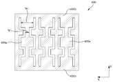
상기 투명전극 패턴층(400)의 구체적인 형상은 다양하게 변경할 수 있으며, 그 예를 도 3a 및 도 3b에 도시하였다. 다만, 본 발명에 따른 투명전극 패턴층(400)의 형상이 도 3a 및 도 3b에 한정되는 것은 아니다.Specific shapes of the transparent
도 3a 및 도 3b는 본 발명의 다양한 실시예에 따른 투명전극 패턴층(400)의 개략적인 평면도이다.3A and 3B are schematic plan views of a transparent
도 3a 및 도 3b에서 알 수 있듯이, 상기 투명전극 패턴층(400)은 제1 방향(y 방향)으로 형성된 복수 개의 제1 패턴들(400a) 및 상기 제1 방향과 상이한 제2 방향(x 방향)으로 형성된 복수 개의 제2 패턴들(400b)을 포함하여 이루어질 수 있다.As shown in FIGS. 3A and 3B, the transparent
상기 제1 패턴들(400a)은 소정 간격으로 이격 배열되어 있고, 각각의 제1 패턴들(400a)은 상기 제2 패턴들(400b)과 연결되어 있다. 즉, 상기 제1 패턴들(400a) 과 상기 제2 패턴들(400b)은 전체적으로 연결된 구조로 형성된다.The
또한, 도 3b에서 알 수 있듯이, 상기 제1 패턴들(400a)은 제1 폭(W1)을 구비한 영역과 상기 제1 폭(W1)과 상이한 제2 폭(W2)을 구비한 영역을 포함하여 이루어질 수 있다.In addition, as shown in FIG. 3B, the
이상과 같은 제1 패턴들(400a) 및 제2 패턴들(400b)로 이루어진 투명전극 패턴층(400)은 제조공정 중 발생하는 정전기를 방지함과 더불어 터치 감도를 향상시키기 위해서 그 패턴들의 폭을 적절히 조절할 필요가 있다.The transparent
구체적으로 설명하면, 제조공정 중 발생하는 정전기를 방지하기 위해서는 전극의 저항이 작은 것이 유리하고 터치 감도를 향상시키기 위해서는 전극의 저항이 큰 것이 유리하기 때문에 양자를 적절히 조절하여 전극의 저항을 설정하는 것이 바람직한데, 전극의 저항은 전극의 폭에 반비례하는 특성이 있으므로, 결국, 설정된 전극의 저항에 맞도록 전극의 폭을 적절히 조절할 필요가 있다.Specifically, since the resistance of the electrode is advantageous to prevent static electricity generated during the manufacturing process, and the resistance of the electrode is advantageous to improve the touch sensitivity, it is desirable to set the resistance of the electrode by appropriately adjusting both. Although the resistance of the electrode is inversely proportional to the width of the electrode, it is necessary to appropriately adjust the width of the electrode so as to match the resistance of the set electrode.
이와 같은 점을 고려할 때, 상기 투명전극 패턴층(400), 보다 구체적으로는 상기 제1 패턴들(400a) 및 제2 패턴들(400b)의 패턴 폭은 5 ~ 100 ㎛ 범위로 설정할 수 있다. 만약, 상기 투명전극 패턴층(400)의 패턴 폭이 5 ㎛ 미만일 경우에는 전극이 저항이 너무 커져 제조공정 중 발생하는 정전기 방지효과가 떨어질 수 있고, 상기 투명전극 패턴층(400)의 패턴 폭이 100 ㎛를 초과할 경우에는 전극이 저항이 너무 작아져 터치 감도 향상 효과가 떨어질 수 있다.In consideration of this, the pattern width of the transparent
한편, 상기 투명전극 패턴층(400)을 구성하는 패턴들 사이의 이격 거리, 예로서 상기 제1 패턴들(400a) 사이의 이격 거리는 적절히 조절할 수 있는데, 시인성 측면을 고려할 때 그 이격 거리가 너무 큰 것은 바람직하지 않을 수 있다. 보다 구체적으로 설명하면, 상기 투명전극 패턴층(400)을 구성하는 패턴들 영역을 투과하는 광과 상기 투명전극 패턴층(400)을 구성하는 패턴들 사이의 영역을 투과하는 광 사이에는 투과율이 상이하게 되는데, 상기 투명전극 패턴층(400)을 구성하는 패턴들 사이의 이격 거리가 너무 크게 되면, 투과율 차이가 커져서 시인성 측면에서 바람직하지 않을 수 있고, 따라서, 사용자가 인식하지 못할 정도로 상기 이격 거리를 소정 거리 내로 설정하는 것이 바람직하다.On the other hand, the separation distance between the patterns constituting the transparent
이와 같은 투명전극 패턴층(400)은 ITO 등과 같은 투명도전물을 쉐도우 마스크(shadow mask)를 이용하여 증착함으로써 패턴 형성할 수 있다.The transparent
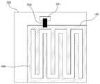
한편, 상기 제1 기판(100)의 일면에 형성된 투명전극 패턴층(400)은 상기 제2 기판(200)을 통해 접지될 수 있는데, 이에 대해서 도 4a 및 도 4b를 참고하여 설명하기로 한다.Meanwhile, the transparent
도 4a 및 도 4b는 각각 본 발명에 따른 투명전극 패턴층(400)이 제2 기판(200)을 통해 접지되는 모습을 도시한 개략적인 평면도 및 단면도이다.4A and 4B are schematic plan views and cross-sectional views illustrating how the transparent
도 4a 및 도 4b에서 알 수 있듯이, 상기 제1 기판(100)의 일면에는 투명전극 패턴층(400)이 형성되어 있고, 상기 제2 기판(200)의 일면에는 접지패드(201)가 형성되어 있다.As shown in FIGS. 4A and 4B, a transparent
또한, 상기 투명전극 패턴층(400)은 도전성 테이프와 같은 도전체(500)를 통해 상기 접지패드(201)와 연결되어 있다. 이와 같이 상기 투명전극 패턴층(400)이 상기 제2 기판(200)을 통해 접지되어 있기 때문에 공정 중에 기판에 정전기가 발생 하는 것이 방지된다.In addition, the transparent
다시 도 2를 참조하면, 상기 제1 기판(100)의 타면, 보다 구체적으로는, 상기 제2 기판(200)과 마주하는 상기 제1 기판(100)의 타면에는 차광층(120)이 형성되어 있다.Referring to FIG. 2 again, a
상기 차광층(120)은 화소영역 이외의 영역으로 광이 누설되는 것을 차단하는 역할을 하는 것으로서, 매트릭스(matrix)구조로 패턴형성되어 있다. 또한, 상기 차광층(120)은 센싱 전극으로 기능할 수도 있으며, 이 경우는 상기 차광층(120)이 도전물질을 포함하여 이루어지고, 또한 터치 신호를 인가하기 위한 신호인가부가 상기 차광층(120)에 연결된다.The
상기 차광층(120) 사이에는 적색(R), 녹색(G), 및 청색(B)의 컬러필터층(140)이 형성되어 있다. 상기 컬러필터층(140)은 도시된 바와 같이, 적색(R), 녹색(G), 및 청색(B)의 필터층 이외에 황색(Y), 백색(W) 또는 시안(CYAN)색의 필터층이 추가로 형성될 수도 있다.A
상기 컬러필터층(140) 상에는 기판 평탄화를 위한 오버코트층(160)이 형성되어 있다.An
상기 제2 기판(200) 상에는 화소영역을 정의하는 게이트 라인과 데이터 라인이 서로 교차되도록 형성되어 있고, 상기 게이트 라인과 데이터 라인이 교차하는 영역에 스위칭 소자로서 박막 트랜지스터가 형성되어 있고, 상기 화소영역에는 화소전극과 공통전극이 서로 평행하게 배열되어 있는데, 이와 같은 제2 기판(200)의 구성에 대해서 설명하면 하기와 같다. 이하에서 설명하는 제2 기판(200)의 구성은 일 예에 해당하는 것으로서, 본 발명에 따른 액정표시장치의 제2 기판(200)이 반드시 이에 한정되는 것은 아니다.A gate line and a data line defining a pixel region are formed to cross each other on the
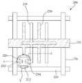
도 5a는 본 발명의 일 실시예에 따른 제2 기판의 평면도이고, 도 5b는 도 5a의 I-I라인에 해당하는 단면도이다. 도 5a 및 도 5b는 액정표시장치의 하나의 화소만을 도시한 것이다.5A is a plan view of a second substrate according to an embodiment of the present invention, and FIG. 5B is a cross-sectional view corresponding to line I-I of FIG. 5A. 5A and 5B show only one pixel of the liquid crystal display.
도 5a에서 알 수 있듯이, 제2 기판(200) 상에는 게이트 라인(210) 및 데이터 라인(230)이 서로 교차하도록 형성되어 있다. 상기 게이트 라인(210)과 데이터 라인(230)이 교차하는 영역에는 박막 트랜지스터(T)가 형성되어 있다.As can be seen in FIG. 5A, the
상기 박막 트랜지스터(T)는 게이트 전극(212), 반도체층(220), 소스 전극(232), 드레인 전극(234)을 포함하여 이루어진다.The thin film transistor T includes a
상기 게이트 전극(212)은 상기 게이트 라인(210)에서 분지되어 돌출형성되어 있고, 상기 소스 전극(232)은 상기 데이터 라인(230)에서 분지되어 돌출형성되어 있고, 상기 드레인 전극(234)은 상기 소스 전극(232)과 소정 간격으로 이격되어 있다.The
이와 같은 박막 트랜지스터(T)에는 화소 전극(240)이 연결되어 있는데, 구체적으로, 상기 화소 전극(240)은 상기 박막 트랜지스터(T)의 드레인 전극(234)과 연결되어 있다.The
또한, 상기 화소 전극(240)과 함께 수평 전계를 형성하기 위해서 상기 화소 전극(240)과 평행하게 공통 전극(250)이 배열되어 있다. 상기 공통전극(250)은 공통라인(252)에서 분지되어 있다. 상기 공통전극(250)은 센싱 전극으로 기능할 수도 있으며, 이 경우는 터치 신호를 인가하기 위한 신호인가부가 상기 공통전극(250)과 연결된다.In addition, the
도 5b에서 알 수 있듯이, 상기 제2 기판(200) 상에는 게이트 전극(212)이 형성되어 있고, 상기 게이트 전극(212)을 포함한 제2 기판(200) 상에는 게이트 절연막(215)이 형성되어 있다. 상기 게이트 절연막(215) 상에는 반도체층(220)이 형성되어 있고, 상기 반도체층(220) 상에는 소스/드레인 전극(232, 234)이 소정 간격으로 이격 형성되어 있다. 또한, 상기 반도체층(220)은 상기 소스/드레인 전극(232, 234)과 접촉하는 영역에 불순물이 도핑된 오믹 콘택층(222)이 구비되어 있다. 상기 소스/드레인 전극(232, 234) 상에는 보호막(245)이 형성되어 있다.As shown in FIG. 5B, a
한편, 화소영역에는 화소전극(240)과 공통전극(250)이 형성되어 있다.On the other hand, the
상기 화소전극(240)은 상기 게이트 절연막(215) 상에 형성되어 있다. 즉, 상기 화소전극(240)은 상기 소스/드레인 전극(232, 234)과 동일층에 형성되어 있으며, 특히 상기 드레인 전극(234)에서 연장되어 형성되어 있다.The
상기 공통전극(250)은 상기 게이트 절연막(215) 하부의 제2 기판(200) 상에 형성되어 있다. 즉, 상기 공통전극(250)은 상기 게이트 전극(212)과 동일층에 형성되어 있다.The
도 6a는 본 발명의 다른 실시예에 따른 제2 기판의 평면도이고, 도 6b는 도 6a의 I-I라인에 해당하는 단면도로서, 이는 공통전극(250) 및 공통라인(252)의 형성 위치만을 제외하고 전술한 도 5a 및 도 5b에 따른 제2 기판과 동일하다. 따라서, 동일한 구성에 대해서 동일한 도면부호를 부여하였고, 동일한 구성에 대한 구 체적인 설명은 생략하기로 한다.FIG. 6A is a plan view of a second substrate according to another embodiment of the present invention, and FIG. 6B is a cross-sectional view corresponding to line II of FIG. 6A, except for forming positions of the
도 6a 및 도 6b에 따르면, 상기 공통전극(250) 및 공통라인(252)이 보호막(245)의 상부에 형성되어 있다.6A and 6B, the
이상 설명한 제2 기판(200)의 구조에서는 상기 화소전극(240)과 상기 공통전극(250)이 서로 상이한 층에 형성되면서 수평 전계를 인가할 수 있도록 구성되어 있지만, 반드시 그에 한정되는 것은 아니고, 상기 화소전극(240)과 상기 공통전극(250)이 서로 동일한 층에 형성되면서 수평 전계를 인가할 수 있도록 구성될 수도 있다. 예를 들어, 상기 화소전극(240)과 상기 공통전극(250)는 상기 보호막(245) 상부에 함께 형성될 수도 있고, 상기 게이트 절연막(215) 상에 함께 형성될 수도 있다.In the structure of the
한편, 도시하지는 않았지만, 상기 제1 기판(100) 및 상기 제2 기판(200) 상에는 배향막이 각각 형성될 수 있다. 상기 배향막은 상기 액정층(300)의 초기 배향을 위한 것으로서, 상기 제1 기판(100) 및 제2 기판(200)의 최상층에 형성된다.Although not illustrated, an alignment layer may be formed on the
또한, 상기 제1 기판(100) 및 상기 제2 기판(200)은 기판의 외곽에 형성된 씰런트(sealant)에 의해 합착 되어 있으며, 상기 제1 기판(100) 및 상기 제2 기판(200) 사이의 셀갭을 유지하기 위해서 스페이서가 추가로 형성될 수 있다.In addition, the
도 1은 종래의 액정표시장치의 개략적인 단면도이다.1 is a schematic cross-sectional view of a conventional liquid crystal display device.
도 2는 본 발명의 일 실시예에 따른 액정표시장치의 개략적인 단면도이다.2 is a schematic cross-sectional view of a liquid crystal display according to an exemplary embodiment of the present invention.
도 3a 및 도 3b는 본 발명의 다양한 실시예에 따른 투명전극 패턴층의 개략적인 평면도이다.3A and 3B are schematic plan views of a transparent electrode pattern layer according to various embodiments of the present disclosure.
도 4a 및 도 4b는 각각 본 발명에 따른 투명전극 패턴층이 제2 기판을 통해 접지되는 모습을 도시한 개략적인 평면도 및 단면도이다.4A and 4B are schematic plan views and cross-sectional views illustrating a state in which a transparent electrode pattern layer according to the present invention is grounded through a second substrate, respectively.
도 5a는 본 발명의 일 실시예에 따른 제2 기판의 평면도이고, 도 5b는 도 5a의 I-I라인에 해당하는 단면도이다.5A is a plan view of a second substrate according to an embodiment of the present invention, and FIG. 5B is a cross-sectional view corresponding to line I-I of FIG. 5A.
도 6a는 본 발명의 다른 실시예에 따른 제2 기판의 평면도이고, 도 6b는 도 6a의 I-I라인에 해당하는 단면도이다.6A is a plan view of a second substrate according to another exemplary embodiment of the present invention, and FIG. 6B is a cross-sectional view corresponding to line I-I of FIG. 6A.
<도면의 주요부 구성에 대한 부호의 설명><Description of the code | symbol about the structure of the principal part of drawing>
100: 제1 기판 120: 차광층100: first substrate 120: light shielding layer
140: 컬러필터층 160: 오버 코트층140: color filter layer 160: overcoat layer
200: 제2 기판 201: 접지패드200: second substrate 201: ground pad
300: 액정층 400: 투명전극 패턴층300: liquid crystal layer 400: transparent electrode pattern layer
Claims (10)
Translated fromKoreanPriority Applications (5)
| Application Number | Priority Date | Filing Date | Title |
|---|---|---|---|
| KR1020090111480AKR20110054725A (en) | 2009-11-18 | 2009-11-18 | LCD Display |
| PL10165404TPL2325690T3 (en) | 2009-11-18 | 2010-06-09 | Liquid crystal display device |
| EP10165404.4AEP2325690B1 (en) | 2009-11-18 | 2010-06-09 | Liquid crystal display device |
| CN2010102121977ACN102062964A (en) | 2009-11-18 | 2010-06-22 | Liquid crystal display device |
| US12/827,996US20110115739A1 (en) | 2009-11-18 | 2010-06-30 | Liquid crystal display device |
Applications Claiming Priority (1)
| Application Number | Priority Date | Filing Date | Title |
|---|---|---|---|
| KR1020090111480AKR20110054725A (en) | 2009-11-18 | 2009-11-18 | LCD Display |
Publications (1)
| Publication Number | Publication Date |
|---|---|
| KR20110054725Atrue KR20110054725A (en) | 2011-05-25 |
Family
ID=43499956
Family Applications (1)
| Application Number | Title | Priority Date | Filing Date |
|---|---|---|---|
| KR1020090111480ACeasedKR20110054725A (en) | 2009-11-18 | 2009-11-18 | LCD Display |
Country Status (5)
| Country | Link |
|---|---|
| US (1) | US20110115739A1 (en) |
| EP (1) | EP2325690B1 (en) |
| KR (1) | KR20110054725A (en) |
| CN (1) | CN102062964A (en) |
| PL (1) | PL2325690T3 (en) |
Cited By (4)
| Publication number | Priority date | Publication date | Assignee | Title |
|---|---|---|---|---|
| KR20120139373A (en)* | 2011-06-17 | 2012-12-27 | 엘지디스플레이 주식회사 | Display device and manufacturing method thereof |
| KR20130142057A (en)* | 2012-06-18 | 2013-12-27 | 삼성디스플레이 주식회사 | Organic light emitting display device |
| KR20150075604A (en)* | 2013-12-26 | 2015-07-06 | 엘지디스플레이 주식회사 | Flexible display device and method of manufacturing the same |
| US11379172B2 (en) | 2018-10-17 | 2022-07-05 | Samsung Display Co., Ltd. | Display device including a plurality of inspection pads |
Families Citing this family (13)
| Publication number | Priority date | Publication date | Assignee | Title |
|---|---|---|---|---|
| JP2015121829A (en)* | 2012-04-18 | 2015-07-02 | シャープ株式会社 | Color filter integrated touch panel |
| US9001280B2 (en) | 2012-06-08 | 2015-04-07 | Apple Inc. | Devices and methods for shielding displays from electrostatic discharge |
| KR20140024149A (en)* | 2012-08-20 | 2014-02-28 | 삼성전기주식회사 | Touch panel and method for manufacturing the same |
| CN102955303B (en)* | 2012-10-26 | 2016-04-06 | 北京京东方光电科技有限公司 | A kind of touching display screen and touch control display apparatus |
| FR2998682B1 (en)* | 2012-11-26 | 2016-01-15 | Volfoni R&D | OPTICAL POLARIZATION MODULATOR WITH LIQUID CRYSTALS |
| TWI584028B (en)* | 2012-12-28 | 2017-05-21 | 鴻海精密工業股份有限公司 | Liquid crystal display panel and thin film transistor substrate |
| EP2887185B1 (en)* | 2013-12-20 | 2016-11-09 | LG Display Co., Ltd. | Display device integrated with touch screen panel and method of driving the same |
| JP2016206322A (en)* | 2015-04-20 | 2016-12-08 | 三菱電機株式会社 | Liquid crystal display |
| CN105425443A (en)* | 2015-12-04 | 2016-03-23 | 江西沃格光电股份有限公司 | Embedded touch screen with high-resistance film and display device |
| CN105425455A (en)* | 2015-12-31 | 2016-03-23 | 武汉华星光电技术有限公司 | Embedded touch display panel and preparation technology thereof |
| US10788943B2 (en)* | 2016-12-15 | 2020-09-29 | Sharp Kabushiki Kaisha | Touch panel-equipped display device |
| CN107229164B (en)* | 2017-07-20 | 2020-10-09 | 武汉华星光电技术有限公司 | Color film substrate and liquid crystal panel manufacturing equipment |
| KR102555984B1 (en)* | 2018-07-27 | 2023-07-14 | 삼성디스플레이 주식회사 | Display device with a force sensor |
Family Cites Families (13)
| Publication number | Priority date | Publication date | Assignee | Title |
|---|---|---|---|---|
| JP2758864B2 (en)* | 1995-10-12 | 1998-05-28 | 株式会社日立製作所 | Liquid crystal display |
| US6086979A (en)* | 1997-11-11 | 2000-07-11 | Hitachi Chemical Company, Ltd. | Electromagnetically shielding bonding film, and shielding assembly and display device using such film |
| JP3107078B2 (en)* | 1999-02-26 | 2000-11-06 | 日本電気株式会社 | Liquid crystal display |
| CN1288951C (en)* | 2001-03-02 | 2006-12-06 | 日立化成工业株式会社 | Electromagnetic wave shielding film, electromagnetic wave shielding component and display |
| TW526706B (en)* | 2002-06-28 | 2003-04-01 | Ponwei Hou | Materials for electromagnetic wave shielding film |
| CN102981678B (en)* | 2006-06-09 | 2015-07-22 | 苹果公司 | Touch screen liquid crystal display |
| US8259078B2 (en)* | 2006-06-09 | 2012-09-04 | Apple Inc. | Touch screen liquid crystal display |
| CN101131618A (en)* | 2006-08-20 | 2008-02-27 | 陈其良 | Pixel-multiplexing touch control type flat panel display |
| JP4501933B2 (en)* | 2006-12-26 | 2010-07-14 | エプソンイメージングデバイス株式会社 | Liquid crystal display |
| US7796224B2 (en)* | 2006-12-26 | 2010-09-14 | Sony Corporation | Liquid crystal display device |
| JP2008281616A (en)* | 2007-05-08 | 2008-11-20 | Seiko Epson Corp | Liquid crystal device and electronic device |
| TWM343210U (en)* | 2008-05-30 | 2008-10-21 | Tpk Touch Solutions Inc | Display panel integrating the touch-control structure |
| US8508495B2 (en)* | 2008-07-03 | 2013-08-13 | Apple Inc. | Display with dual-function capacitive elements |
- 2009
- 2009-11-18KRKR1020090111480Apatent/KR20110054725A/ennot_activeCeased
- 2010
- 2010-06-09EPEP10165404.4Apatent/EP2325690B1/enactiveActive
- 2010-06-09PLPL10165404Tpatent/PL2325690T3/enunknown
- 2010-06-22CNCN2010102121977Apatent/CN102062964A/enactivePending
- 2010-06-30USUS12/827,996patent/US20110115739A1/ennot_activeAbandoned
Cited By (4)
| Publication number | Priority date | Publication date | Assignee | Title |
|---|---|---|---|---|
| KR20120139373A (en)* | 2011-06-17 | 2012-12-27 | 엘지디스플레이 주식회사 | Display device and manufacturing method thereof |
| KR20130142057A (en)* | 2012-06-18 | 2013-12-27 | 삼성디스플레이 주식회사 | Organic light emitting display device |
| KR20150075604A (en)* | 2013-12-26 | 2015-07-06 | 엘지디스플레이 주식회사 | Flexible display device and method of manufacturing the same |
| US11379172B2 (en) | 2018-10-17 | 2022-07-05 | Samsung Display Co., Ltd. | Display device including a plurality of inspection pads |
Also Published As
| Publication number | Publication date |
|---|---|
| US20110115739A1 (en) | 2011-05-19 |
| EP2325690A3 (en) | 2011-12-14 |
| EP2325690B1 (en) | 2016-07-20 |
| PL2325690T3 (en) | 2017-01-31 |
| CN102062964A (en) | 2011-05-18 |
| EP2325690A2 (en) | 2011-05-25 |
Similar Documents
| Publication | Publication Date | Title |
|---|---|---|
| KR20110054725A (en) | LCD Display | |
| US9971210B2 (en) | Liquid crystal display device | |
| US8692948B2 (en) | Electric field shielding for in-cell touch type thin-film-transistor liquid crystal displays | |
| US8289457B2 (en) | Liquid crystal display including touch sensor layer and manufacturing method thereof | |
| KR101538934B1 (en) | Display panel and manufacturing method of the same | |
| US8792061B2 (en) | Liquid crystal display device | |
| KR101385190B1 (en) | Liquid crystal display and manufacturing method of the same | |
| CN109117016B (en) | Display panel and manufacturing method thereof | |
| KR102015015B1 (en) | Liquid crystal display | |
| KR101571683B1 (en) | Display panel and manufacturing method of the same | |
| KR20090075369A (en) | Display panel | |
| US20110187669A1 (en) | Liquid crystal display device and manufacting method thereof | |
| WO2017117966A1 (en) | Colour film substrate and embedded touch control display apparatus | |
| KR20120009782A (en) | LCD Display | |
| KR20090026576A (en) | Display device and manufacturing method thereof | |
| US20130076996A1 (en) | Integrated touch panel with display device and method of manufacturing the same | |
| US20110317115A1 (en) | Liquid crystal display device and method for manufacturing same | |
| US11150502B2 (en) | Display substrate and display device | |
| CN214586297U (en) | Display device and detection device | |
| CN112684941B (en) | Built-in touch display panel | |
| KR101820661B1 (en) | Liquid crystal display device | |
| KR101950434B1 (en) | Liquid crystal display device | |
| KR20200076312A (en) | Touch panel liquid crystal display device |
Legal Events
| Date | Code | Title | Description |
|---|---|---|---|
| PA0109 | Patent application | Patent event code:PA01091R01D Comment text:Patent Application Patent event date:20091118 | |
| PG1501 | Laying open of application | ||
| A201 | Request for examination | ||
| PA0201 | Request for examination | Patent event code:PA02012R01D Patent event date:20111028 Comment text:Request for Examination of Application Patent event code:PA02011R01I Patent event date:20091118 Comment text:Patent Application | |
| E902 | Notification of reason for refusal | ||
| PE0902 | Notice of grounds for rejection | Comment text:Notification of reason for refusal Patent event date:20130129 Patent event code:PE09021S01D | |
| AMND | Amendment | ||
| E601 | Decision to refuse application | ||
| PE0601 | Decision on rejection of patent | Patent event date:20130731 Comment text:Decision to Refuse Application Patent event code:PE06012S01D Patent event date:20130129 Comment text:Notification of reason for refusal Patent event code:PE06011S01I | |
| AMND | Amendment | ||
| PX0901 | Re-examination | Patent event code:PX09011S01I Patent event date:20130731 Comment text:Decision to Refuse Application Patent event code:PX09012R01I Patent event date:20130227 Comment text:Amendment to Specification, etc. | |
| E90F | Notification of reason for final refusal | ||
| PE0902 | Notice of grounds for rejection | Comment text:Final Notice of Reason for Refusal Patent event date:20131031 Patent event code:PE09021S02D | |
| AMND | Amendment | ||
| PX0601 | Decision of rejection after re-examination | Comment text:Decision to Refuse Application Patent event code:PX06014S01D Patent event date:20140430 Comment text:Amendment to Specification, etc. Patent event code:PX06012R01I Patent event date:20131118 Comment text:Final Notice of Reason for Refusal Patent event code:PX06013S02I Patent event date:20131031 Comment text:Amendment to Specification, etc. Patent event code:PX06012R01I Patent event date:20130819 Comment text:Decision to Refuse Application Patent event code:PX06011S01I Patent event date:20130731 Comment text:Amendment to Specification, etc. Patent event code:PX06012R01I Patent event date:20130227 Comment text:Notification of reason for refusal Patent event code:PX06013S01I Patent event date:20130129 | |
| J201 | Request for trial against refusal decision | ||
| PJ0201 | Trial against decision of rejection | Patent event date:20140529 Comment text:Request for Trial against Decision on Refusal Patent event code:PJ02012R01D Patent event date:20140430 Comment text:Decision to Refuse Application Patent event code:PJ02011S01I Patent event date:20130731 Comment text:Decision to Refuse Application Patent event code:PJ02011S01I Appeal kind category:Appeal against decision to decline refusal Appeal identifier:2014101003279 Request date:20140529 | |
| J301 | Trial decision | Free format text:TRIAL DECISION FOR APPEAL AGAINST DECISION TO DECLINE REFUSAL REQUESTED 20140529 Effective date:20141230 | |
| PJ1301 | Trial decision | Patent event code:PJ13011S01D Patent event date:20141230 Comment text:Trial Decision on Objection to Decision on Refusal Appeal kind category:Appeal against decision to decline refusal Request date:20140529 Decision date:20141230 Appeal identifier:2014101003279 |