KR20110050423A - Application-Specific Injection Systems and Methods for Use in Solar Cell Fabrication - Google Patents
Application-Specific Injection Systems and Methods for Use in Solar Cell FabricationDownload PDFInfo
- Publication number
- KR20110050423A KR20110050423AKR1020117000362AKR20117000362AKR20110050423AKR 20110050423 AKR20110050423 AKR 20110050423AKR 1020117000362 AKR1020117000362 AKR 1020117000362AKR 20117000362 AKR20117000362 AKR 20117000362AKR 20110050423 AKR20110050423 AKR 20110050423A
- Authority
- KR
- South Korea
- Prior art keywords
- substrate
- ion source
- light
- gridline
- receiving region
- Prior art date
- Legal status (The legal status is an assumption and is not a legal conclusion. Google has not performed a legal analysis and makes no representation as to the accuracy of the status listed.)
- Withdrawn
Links
Images


Classifications
- H—ELECTRICITY
- H01—ELECTRIC ELEMENTS
- H01L—SEMICONDUCTOR DEVICES NOT COVERED BY CLASS H10
- H01L21/00—Processes or apparatus adapted for the manufacture or treatment of semiconductor or solid state devices or of parts thereof
- H01L21/02—Manufacture or treatment of semiconductor devices or of parts thereof
- H01L21/04—Manufacture or treatment of semiconductor devices or of parts thereof the devices having potential barriers, e.g. a PN junction, depletion layer or carrier concentration layer
- H01L21/18—Manufacture or treatment of semiconductor devices or of parts thereof the devices having potential barriers, e.g. a PN junction, depletion layer or carrier concentration layer the devices having semiconductor bodies comprising elements of Group IV of the Periodic Table or AIIIBV compounds with or without impurities, e.g. doping materials
- H01L21/26—Bombardment with radiation
- H01L21/263—Bombardment with radiation with high-energy radiation
- H01L21/265—Bombardment with radiation with high-energy radiation producing ion implantation
- H01L21/266—Bombardment with radiation with high-energy radiation producing ion implantation using masks
- H—ELECTRICITY
- H01—ELECTRIC ELEMENTS
- H01L—SEMICONDUCTOR DEVICES NOT COVERED BY CLASS H10
- H01L21/00—Processes or apparatus adapted for the manufacture or treatment of semiconductor or solid state devices or of parts thereof
- H01L21/02—Manufacture or treatment of semiconductor devices or of parts thereof
- H01L21/04—Manufacture or treatment of semiconductor devices or of parts thereof the devices having potential barriers, e.g. a PN junction, depletion layer or carrier concentration layer
- H01L21/18—Manufacture or treatment of semiconductor devices or of parts thereof the devices having potential barriers, e.g. a PN junction, depletion layer or carrier concentration layer the devices having semiconductor bodies comprising elements of Group IV of the Periodic Table or AIIIBV compounds with or without impurities, e.g. doping materials
- H01L21/26—Bombardment with radiation
- H01L21/263—Bombardment with radiation with high-energy radiation
- H01L21/265—Bombardment with radiation with high-energy radiation producing ion implantation
- H01L21/26506—Bombardment with radiation with high-energy radiation producing ion implantation in group IV semiconductors
- H01L21/26513—Bombardment with radiation with high-energy radiation producing ion implantation in group IV semiconductors of electrically active species
- H—ELECTRICITY
- H01—ELECTRIC ELEMENTS
- H01L—SEMICONDUCTOR DEVICES NOT COVERED BY CLASS H10
- H01L21/00—Processes or apparatus adapted for the manufacture or treatment of semiconductor or solid state devices or of parts thereof
- H01L21/02—Manufacture or treatment of semiconductor devices or of parts thereof
- H01L21/04—Manufacture or treatment of semiconductor devices or of parts thereof the devices having potential barriers, e.g. a PN junction, depletion layer or carrier concentration layer
- H01L21/18—Manufacture or treatment of semiconductor devices or of parts thereof the devices having potential barriers, e.g. a PN junction, depletion layer or carrier concentration layer the devices having semiconductor bodies comprising elements of Group IV of the Periodic Table or AIIIBV compounds with or without impurities, e.g. doping materials
- H01L21/26—Bombardment with radiation
- H01L21/263—Bombardment with radiation with high-energy radiation
- H01L21/265—Bombardment with radiation with high-energy radiation producing ion implantation
- H01L21/2658—Bombardment with radiation with high-energy radiation producing ion implantation of a molecular ion, e.g. decaborane
- H—ELECTRICITY
- H10—SEMICONDUCTOR DEVICES; ELECTRIC SOLID-STATE DEVICES NOT OTHERWISE PROVIDED FOR
- H10F—INORGANIC SEMICONDUCTOR DEVICES SENSITIVE TO INFRARED RADIATION, LIGHT, ELECTROMAGNETIC RADIATION OF SHORTER WAVELENGTH OR CORPUSCULAR RADIATION
- H10F10/00—Individual photovoltaic cells, e.g. solar cells
- H10F10/10—Individual photovoltaic cells, e.g. solar cells having potential barriers
- H10F10/16—Photovoltaic cells having only PN heterojunction potential barriers
- H—ELECTRICITY
- H10—SEMICONDUCTOR DEVICES; ELECTRIC SOLID-STATE DEVICES NOT OTHERWISE PROVIDED FOR
- H10F—INORGANIC SEMICONDUCTOR DEVICES SENSITIVE TO INFRARED RADIATION, LIGHT, ELECTROMAGNETIC RADIATION OF SHORTER WAVELENGTH OR CORPUSCULAR RADIATION
- H10F71/00—Manufacture or treatment of devices covered by this subclass
- H10F71/121—The active layers comprising only Group IV materials
- H—ELECTRICITY
- H10—SEMICONDUCTOR DEVICES; ELECTRIC SOLID-STATE DEVICES NOT OTHERWISE PROVIDED FOR
- H10F—INORGANIC SEMICONDUCTOR DEVICES SENSITIVE TO INFRARED RADIATION, LIGHT, ELECTROMAGNETIC RADIATION OF SHORTER WAVELENGTH OR CORPUSCULAR RADIATION
- H10F77/00—Constructional details of devices covered by this subclass
- H10F77/20—Electrodes
- H10F77/206—Electrodes for devices having potential barriers
- H10F77/211—Electrodes for devices having potential barriers for photovoltaic cells
- Y—GENERAL TAGGING OF NEW TECHNOLOGICAL DEVELOPMENTS; GENERAL TAGGING OF CROSS-SECTIONAL TECHNOLOGIES SPANNING OVER SEVERAL SECTIONS OF THE IPC; TECHNICAL SUBJECTS COVERED BY FORMER USPC CROSS-REFERENCE ART COLLECTIONS [XRACs] AND DIGESTS
- Y02—TECHNOLOGIES OR APPLICATIONS FOR MITIGATION OR ADAPTATION AGAINST CLIMATE CHANGE
- Y02E—REDUCTION OF GREENHOUSE GAS [GHG] EMISSIONS, RELATED TO ENERGY GENERATION, TRANSMISSION OR DISTRIBUTION
- Y02E10/00—Energy generation through renewable energy sources
- Y02E10/50—Photovoltaic [PV] energy
- Y02E10/547—Monocrystalline silicon PV cells
- Y—GENERAL TAGGING OF NEW TECHNOLOGICAL DEVELOPMENTS; GENERAL TAGGING OF CROSS-SECTIONAL TECHNOLOGIES SPANNING OVER SEVERAL SECTIONS OF THE IPC; TECHNICAL SUBJECTS COVERED BY FORMER USPC CROSS-REFERENCE ART COLLECTIONS [XRACs] AND DIGESTS
- Y02—TECHNOLOGIES OR APPLICATIONS FOR MITIGATION OR ADAPTATION AGAINST CLIMATE CHANGE
- Y02P—CLIMATE CHANGE MITIGATION TECHNOLOGIES IN THE PRODUCTION OR PROCESSING OF GOODS
- Y02P70/00—Climate change mitigation technologies in the production process for final industrial or consumer products
- Y02P70/50—Manufacturing or production processes characterised by the final manufactured product
Landscapes
- Physics & Mathematics (AREA)
- Engineering & Computer Science (AREA)
- High Energy & Nuclear Physics (AREA)
- Computer Hardware Design (AREA)
- Toxicology (AREA)
- Condensed Matter Physics & Semiconductors (AREA)
- General Physics & Mathematics (AREA)
- Manufacturing & Machinery (AREA)
- Health & Medical Sciences (AREA)
- Microelectronics & Electronic Packaging (AREA)
- Power Engineering (AREA)
- Spectroscopy & Molecular Physics (AREA)
- Photovoltaic Devices (AREA)
- Life Sciences & Earth Sciences (AREA)
- Sustainable Development (AREA)
- Sustainable Energy (AREA)
Abstract
Translated fromKoreanDescription
Translated fromKorean본 발명은, 발명의 명칭이 "SOLAR CELL FABRICATION USING IMPLANTATION"이고, 2008년 6월 11일 출원되어 공동 계류중인 미국 가특허출원 제 61/131,687호, 발명의 명칭이 "APPLICATIONS SPECIFIC IMPLANTATION SYSTEM FOR USE IN SOLAR CELL FABRICATIONS"이고, 2008년 6월 11일 출원되어 공동 계류중인 미국 가특허 출원 제 61/131,688호, 발명의 명칭이 "FORMATION OF SOLAR CELL-SELECTIVE EMITTER USING IMPLANT AND ANNEAL METHOD"이고, 2008년 6월 11일 출원되어 공동 계류중인 미국 가특허출원 제 61/131,698호, 발명의 명칭이 "SOLAR CELL FABRICATION WITH FACETING AND IMPLANTATION"이고, 2008년 6월 24일 출원되어 공동 계류중인 미국 가특허출원 제 61/133,028호, 및 발명의 명칭이 "ADVANCED HIGH EFFICIENCY CRYSTALLINE SOLAR CELL FABRICATION METHOD"이고, 2009년 3월 20일에 출원되어 공동 계류중인 미국 가특허출원 제 61/210,545호에 대하여, 35 U.S.C.§119(e)하에 우선권을 주장하며, 이들 모두 본 명세서에서 설명되는 것처럼 참조로서 본 명세서에서 병합된다.The present invention, the name of the invention "SOLAR CELL FABRICATION USING IMPLANTATION", US Provisional Patent Application No. 61 / 131,687, filed June 11, 2008, co-pending, the name of the invention "APPLICATIONS SPECIFIC IMPLANTATION SYSTEM FOR USE IN SOLAR CELL FABRICATIONS ", co-pending US Provisional Patent Application No. 61 / 131,688, filed June 11, 2008, entitled" FORMATION OF SOLAR CELL-SELECTIVE EMITTER USING IMPLANT AND ANNEAL METHOD ", 6 2008 United States Provisional Patent Application No. 61 / 131,698, filed May 11, titled "SOLAR CELL FABRICATION WITH FACETING AND IMPLANTATION", and co-pending US Provisional Patent Application No. 61, filed June 24, 2008 / 133,028, and the invention entitled "ADVANCED HIGH EFFICIENCY CRYSTALLINE SOLAR CELL FABRICATION METHOD", and 35 USC§119 (for US Provisional Patent Application 61 / 210,545, filed March 20, 2009). e) Priority under And claims, all of which are incorporated herein by reference as if set forth herein.
본 발명은 반도체 디바이스의 제조에 관한 것이다. 더 구체적으로, 본 발명은 솔라 셀 제조를 위한 시스템 및 방법에 관한 것이다.The present invention relates to the manufacture of semiconductor devices. More specifically, the present invention relates to systems and methods for solar cell manufacture.
반도체 디바이스는 다-목적 반도체 제작 툴(tool)을 사용하여 제조된다. 현재 반도체 디바이스의 계속-작아지는 치수에 기인하여, 이들 툴은 엄격한 규격에 따라 디바이스를 제작한다. 다-목적이기 때문에, 이들 툴은 넓은 범위의 에너지에 걸치는(span) 빔을 사용하여, 상이한 제작 단계에 대해 상이한 이온(ion)종을 생성한다. 작은-외형의 디바이스를 제작할 수 있기 위해 이들 툴은 엄격한 스캐닝(scanning) 치수를 갖는다. 또한, 이들 툴은 기판상에 수집된 전하를 중화시키기 위해 오염을 감소시키고, 특정 모듈을 포함하기 위하여 질량(mass) 분석을 수행한다. 이들 툴이 매우 복잡하고, 이들의 요구사항이 매우 엄격하기에, 이들의 생산량은 비교적 적은, 오직 시간당 대략 200개의 웨이퍼(wafer)이다.Semiconductor devices are fabricated using multi-purpose semiconductor fabrication tools. Due to the ever-smaller dimensions of current semiconductor devices, these tools manufacture devices according to strict specifications. As multi-purpose, these tools use beams that span a wide range of energy, producing different ion species for different fabrication steps. These tools have strict scanning dimensions in order to be able to manufacture small-appearance devices. In addition, these tools reduce contamination to neutralize the charge collected on the substrate and perform mass analysis to include specific modules. Because these tools are very complex and their requirements are very stringent, their yield is only about 200 wafers per hour, which is relatively small.
도 1은 반도체 디바이스를 제조하는 하나의 단계로서, 기판에 주입하기 위한 종래 기술의 주입 시스템(100)을 도시한다. 다수의 웨이퍼는 트윈 로드 락(twin load lock)(105)을 통하여 시스템(100)에 도입(introduce)된다. 다수의 가스 전달 모듈(110)은 다수의 가스를 포함할 수 있는데, n-타입 및 p-타입 이온(불순물(dopant))은 상기 다수의 가스로부터 추출된다. 이 이온은 사전-가속 장치(120)에 의해 가속되는데, 이 사전-가속 장치(120)는 오염을 감소시키기 위하여 질량 분석을 수행하는 자석(magnet)(125)에 이들 이온을 전달한다. 그런 후에, 이온은 후-가속 장치(130)에 전달되어, 전하 중화 모듈(135)로 전달된다. 이온의 빔은 빔 스캐닝 메카니즘(140)을 사용하여 다수의 웨이퍼(101)의 표면을 가로질러 스캔된다; 대안으로, 웨이퍼(101) 그 자체가 빔에 대하여 이동된다. 그런 후에, 측정 및 제어 유닛(145)은 웨이퍼(101)를 분석한다.1 illustrates a prior
시스템(100)이 상이한 불순물을 주입할 수 있어야 하기 때문에, 사전 가속 장치(120) 및 자석(125)의 작동 범위는 커야만 하는데, 일반적으로 10keV 미만에서 200keV 이므로, 모든 불순물 타입을 주입하는데 충분하다. 또한 이 시스템(100)은 진보된 형태의 엄중한 요구사항(65nm 보다 작은)을 충족할 수 있어야 한다. 하나의 예시로서, 0.5% 미만의 균일성 요구사항은 다중 빔 스캔을 요구하여, 시스템 생산성을 감소시킨다.Since the
제 2 단점은 디바이스상에 특징부가 디바이스의 제조의 상이한 단계 동안 변하는데 있다. 이들 특징부는 이들 특징부가 노출되는 높은 온도 또는, 수집된 전하에 버틸 수 없다. 게다가, 특징부 그 자체는, 예를 들어, 절연 필름이 이 필름의 형성 동안 전하를 수집할 때, 주입 빔에 악영향을 미칠 수 있다.A second disadvantage is that features on the device change during different stages of manufacture of the device. These features cannot withstand the high temperatures or collected charges to which they are exposed. In addition, the features themselves may adversely affect the injection beam, for example when the insulating film collects charge during the formation of this film.
소수의 예외를 제외하고, 디바이스 제작은 높은 전력 밀도 및 고온의 생성을 갖는 빔을 요구한다. 일반적으로 이들 제한은 종래 기술의 제작 시스템을 복잡하게 한다.With a few exceptions, device fabrication requires beams with high power density and high temperature generation. In general, these limitations complicate the prior art fabrication system.
제 1 양상에서, 반도체 기판에 주입하기 위한 시스템은, 이온 소스, 이온 소스로부터의 대략 150keV 이하의 에너지를 갖는 빔을 생성하기 위한 가속 장치, 및 기판을 빔에 노출시키는 빔 디렉터(director)를 포함한다. 하나의 실시예에서, 이온 소스는 단일-가스 전달 요소 및 단일-이온 소스를 포함하는 단일-종의 전달 모듈을 포함한다. 빔 디렉터는 정전기 및 전자기 광학계(optics)와 같은 집속 요소를 포함하는데, 이 요소는 기판 위에 빔을 집속 시키거나 또는 성형하는데 사용된다. 다른 실시에에서, 이온 소스는 추출되는 이온을 생성하는 플라즈마(plasma) 소스(단일-이온 플라즈마 소스와 같은)를 포함한다. 또한, 이러한 다른 실시예는 기판을 둘러싸거나, 또는 그렇지 않으면 이 기판을 전체적으로 커버(cover)하기 위하여 이온을 분산시키는 가속 장치 및 빔 디렉터를 포함한다.In a first aspect, a system for implanting into a semiconductor substrate includes an ion source, an accelerator for generating a beam having energy of approximately 150 keV or less from the ion source, and a beam director that exposes the substrate to the beam. do. In one embodiment, the ion source comprises a single-species delivery module comprising a single-gas delivery element and a single-ion source. The beam director includes focusing elements such as electrostatic and electromagnetic optics, which are used to focus or shape the beam onto the substrate. In another embodiment, the ion source comprises a plasma source (such as a single-ion plasma source) that produces ions to be extracted. This alternative embodiment also includes an accelerator and beam director to disperse the ions to enclose the substrate or otherwise cover the substrate as a whole.
하나의 실시예에서, 단일-이온 플라즈마 소스는 5cm 내지 10cm의 빔 슬롯 길이와 5mm 미만의 폭을 갖는다. 대안으로, 단일-이온 플라즈마 소스는 더 긴 슬롯 길이, 폭, 또는 모두를 갖는다. 추가로, 마그네트론(magnetron)에 의해 생성된 플라즈마 소스는 매우 큰 플라즈마를 생성하기 위하여 생성될 수 있는데, 기판은 구현을 위하여 이 플라즈마 내에 놓일 수 있다. 이온 소스는 안티몬(antimony), 비소(arsenic), 또는 인(phosphorous)과 같은 n-타입 불순물을 포함한다. 물론, 다른 n-타입 불순물 또한 사용될 수 있다. 대안으로, 이온 소스는 붕소(boron), 알루미늄, 갈륨(gallium), 인듐(indium), 또는 BF2와 같은 p-타입 불순물을 포함한다. 다른 p-타입의 불순물 또한 사용될 수 있다.In one embodiment, the single-ion plasma source has a beam slot length of 5 cm to 10 cm and a width of less than 5 mm. Alternatively, the single-ion plasma source has a longer slot length, width, or both. In addition, the plasma source generated by the magnetron can be generated to produce a very large plasma, where the substrate can be placed in this plasma for implementation. Ion sources include n-type impurities such as antimony, arsenic, or phosphorous. Of course, other n-type impurities may also be used. Alternatively, the ion source includes p-type impurities such as boron, aluminum, gallium, indium, or BF2 . Other p-type impurities may also be used.
빔은 대략 5kW/cm2의 전력 밀도를 갖는다. 하나의 실시예에서, 단일-이온 소스는 시스템, 예를 들어, 단일-종의 전달 모듈과 플러그-호환성(plug-compatible)이 있다.The beam has a power density of approximately 5 kW / cm2 . In one embodiment, the single-ion source is plug-compatible with a system, eg, a single-species delivery module.
하나의 실시예에서, 빔 디렉터는 직교 방향으로 기판을 가로질러 빔을 스테핑(step) 하기 위하여 스캐닝 요소를 포함한다.In one embodiment, the beam director includes a scanning element to step the beam across the substrate in an orthogonal direction.
제 2 양상에서, 반도체 디바이스를 제작하는 방법은 기판 내에 광(photo)-수용 영역을 형성하는 단계, 그리드라인(gridlines)을 형성하기 위하여 광-수용 영역을 도핑하는 단계, 및 금속 핑거(fingers)를 그리드라인에 연결하는 단계를 포함한다. 광-수용 영역은 제 1 농도의 불순물로 도핑되고, 및 그리드라인을 형성하기 위하여 제 1 농도보다 높은 제 2 농도의 불순물로 도핑된다. 그리드라인은 광-수용 영역의 가장 높은(topmost) 영역으로부터 기판 아래로 확장한다. 단일-종의 전달 모듈을 포함하는 시스템을 사용하여 광-수용 영역이 도핑되고, 그리드라인이 형성된다. 금속 핑거는 그리드라인에 연결된다. 따라서, 기판은 금속 핑거 아래에 낮은 불순물 분포 및 높은 불순물 분포의 광-수용 영역을 갖는다.In a second aspect, a method of fabricating a semiconductor device includes forming a photo-receiving region in a substrate, doping the light-receiving region to form gridlines, and metal fingers. Connecting to the grid line. The light-receiving region is doped with an impurity of a first concentration and doped with an impurity of a second concentration higher than the first concentration to form a gridline. The gridline extends below the substrate from the topmost region of the light-receiving region. The light-receiving regions are doped and gridlines are formed using a system comprising a single-species delivery module. The metal finger is connected to the grid line. Thus, the substrate has a low impurity distribution and a high impurity distribution light-receiving region under the metal finger.
하나의 실시예에서, 기판은 다른 기판으로부터 개별적으로, 따로따로 도핑된다. 다른 실시예에서, 기판은 다른 기판과 그룹으로 도핑된다.In one embodiment, the substrate is doped separately and separately from the other substrate. In other embodiments, the substrate is doped in groups with other substrates.
하나의 실시예에서, 그리드라인은 마스크(mask)를 통하여 기판을 불순물을 포함하는 이온빔에 노출시킴으로써 형성된다. 이 마스크는 기판의 표면으로부터 떨어져 놓이고 그리드라인의 폭으로 치수가 맞춰진 개구부를 갖는다. 대안으로, 폭은 그리드라인의 폭과는 알려진 편차(deviation)를 갖는다. 다른 실시예에서 마스크는 기판의 표면상에 위치되고, 그리드라인이 형성될 위치에 인접한 개구부를 갖는다. 또 다른 실시예에서, 그리드라인은 불순물을 포함하는 플라즈마 빔을 이 그리드라인의 폭으로 성형 또는 펄싱(pulsing)하고, 빔을 광-수용 영역 위로 향하게 함으로써 형성된다. 이러한 후자의 실시예에서, 플라즈마 빔은 고정적이다. 다른 실시에에서, 이온 빔은 그리드라인을 순차적으로 형성하기 위하여 광-수용 영역을 가로질러 스캔 되거나, 또는 그리드라인을 동시에 형성하기 위하여 생성된다.In one embodiment, gridlines are formed by exposing a substrate to an ion beam containing impurities through a mask. The mask has an opening spaced apart from the surface of the substrate and dimensioned to the width of the gridline. Alternatively, the width has a known deviation from the width of the gridline. In another embodiment the mask is located on the surface of the substrate and has an opening adjacent to where the gridline will be formed. In another embodiment, gridlines are formed by shaping or pulsing a plasma beam containing impurities to the width of the gridline and directing the beam over the light-receiving region. In this latter embodiment, the plasma beam is fixed. In another embodiment, the ion beam is scanned across the light-receiving area to form gridlines sequentially, or generated to form gridlines simultaneously.
하나의 실시예에서, 제 1 농도(조사량(dose))는 1 * 1015/cm2 미만이다. 광-수용 영역은 대략 100Ω/□의 저항을 갖는다. 그리드라인은 대략 10 내지 30Ω/□의 저항을 갖고, 200미크론 미만의 폭을 가지며, 서로 5mm 미만으로 이격된다. 하나의 실시예에서, 그리드라인은 대략 3mm 이격된다.In one embodiment, the first concentration (dose) is less than 1 * 1015 / cm2 . The light-receiving region has a resistance of approximately 100 Ω / square. The grid lines have a resistance of approximately 10-30 ohms / square, have a width of less than 200 microns, and are spaced apart from each other by less than 5 mm. In one embodiment, the grid lines are approximately 3 mm apart.
게다가, 본 방법은 그리드라인을 금속 핑거에 연결하기 전에, 각각의 그리드라인 상에 금속 시드(seed)를 주입하여, 금속 실리사이드(silicide)를 형성하는 단계를 포함한다.In addition, the method includes injecting metal seeds on each gridline to form metal silicides prior to connecting the gridlines to the metal fingers.
하나의 실시예에서, 또한, 본 방법은 예를 들어, 노(furnace), 플래쉬 램프(flash lamp), 또는 레이저를 사용함으로써, 기판을 어닐링(annealing) 하는 단계를 포함한다. 이 기판은 단일 단계에서 저온으로, 예를 들어 400 내지 500℃로 어닐링될 수 있다.In one embodiment, the method also includes annealing the substrate, for example by using a furnace, flash lamp, or laser. The substrate can be annealed to low temperatures, for example 400 to 500 ° C. in a single step.
제 3 양상에서, 솔라 셀을 제작하기 위한 방법은, 150kV 미만의 에너지를 갖는 이온 빔을 사용하여 기판 내의 광-수용 영역을 제 1 농도로 도핑하는 단계, 그리드라인을 형성하기 위하여, 이온 빔을 사용하여 제 1 농도보다 높은 제 2 농도로 광-수용 영역을 도핑하는 단계, 및 금속 핑거를 그리드라인에 연결하는 단계를 포함한다. 그리드라인은 광-수용 영역의 가장 높은 표면으로부터 기판 아래로 확장된다. 기판은 156 mm x 156 mm이고, 광-수용 영역은 단일-종의 전달 모듈을 포함하는 시스템을 사용하여 도핑된다. 시스템은 적어도 시간당 1,000개의 웨이퍼 처리량을 갖는다.In a third aspect, a method for fabricating a solar cell comprises doping a light-receiving region in a substrate to a first concentration using an ion beam having an energy of less than 150 kV, to form a gridline. And doping the light-receiving region to a second concentration higher than the first concentration, and connecting the metal fingers to the gridline. The gridline extends below the substrate from the highest surface of the light-receiving region. The substrate is 156 mm x 156 mm and the light-receiving region is doped using a system comprising a single-species transfer module. The system has at least 1,000 wafer throughputs per hour.
본 발명은 "죽은 층"의 형성을 감소시키고, 콘택트(contact) 저항을 향상시켜서, 이로 인하여 솔라 셀의 효율을 증가시키는 효과를 갖는다.The present invention has the effect of reducing the formation of "dead layers" and improving contact resistance, thereby increasing the efficiency of the solar cell.
도 1은 종래 기술의 반도체 디바이스 제작 시스템을 도시하는 도면.
도 2는 실시예에 따른 반도체 디바이스 제작 시스템을 도시하는 도면.
도 3a 및 도 3b는 실시예에 따른 빔을 성형하기 위한 빔 광학계을 도시하는 도면.
도 4는 일 실시예에 따른 솔라 셀의 약하게 도핑된 광-수용 영역을 도시하는 도면.
도 5a 내지 도 5c는 상이한 실시예에 따라, 도 4의 광-수용 영역을 도핑함으로써 그리드라인의 형성을 도시하는 도면.
도 6은 일 실시예에 따라, 그리드라인을 도 4의 솔라 셀의 금속 핑거에 연결하기 위하여 시드를 사용하는 것을 도시하는 도면.
도 7은 일 실시에에 따라 프로파일 맞춤화(profile tailoring) 그래프를 도시하는 도면.
도 8은 확산(diffusion)을 사용하여 도핑되는 솔라 셀을 위한 프로파일 맞춤화 능력의 단점을 설명하는 그래프.
도 9a 및 도 9b는 하나의 실시예에 따라 이온 주입을 사용하여 도핑되는 솔라 셀에 대한 프로파일 맞춤화 능력의 장점을 설명하는 그래프.
도 10은 하나의 실시예에 따른 솔라 셀을 제작하기 위한 처리의 단계를 도시하는 도면.1 shows a semiconductor device manufacturing system of the prior art.
2 illustrates a semiconductor device manufacturing system according to an embodiment.
3A and 3B illustrate beam optics for shaping a beam according to an embodiment.
4 illustrates a lightly doped light-receiving region of a solar cell according to one embodiment.
5A-5C illustrate the formation of gridlines by doping the light-receiving region of FIG. 4, in accordance with different embodiments.
FIG. 6 illustrates the use of seeds to connect gridlines to metal fingers of the solar cell of FIG. 4, in accordance with an embodiment. FIG.
7 illustrates a profile tailoring graph according to one embodiment.
FIG. 8 is a graph illustrating the disadvantages of profile customization capabilities for solar cells doped using diffusion. FIG.
9A and 9B are graphs illustrating the advantages of profile customization capabilities for solar cells doped using ion implantation in accordance with one embodiment.
10 illustrates a step in a process for fabricating a solar cell according to one embodiment.
본 발명에 따른 시스템은 솔라 셀과 같은 특정 반도체 디바이스를 제작하기 위하여 특별하게 맞추어진다. 이들 시스템은 다른 반도체 디바이스를 제작하기 위하여 요구되는 오차 허용도 보다 더 완화된 오차 허용도를 사용한다. 이들 시스템은 종래 기술의 시스템보다 더 빨리, 덜 비싸게, 그리고 더 작은 공간에서 디바이스를 제작한다. 이러한 시스템은 적어도 시간당 1,000개의 솔라 셀을 생산할 수 있다.The system according to the invention is specifically tailored for fabricating specific semiconductor devices such as solar cells. These systems use error tolerances that are more relaxed than the error tolerances required to fabricate other semiconductor devices. These systems fabricate devices faster, less expensive, and in smaller spaces than prior art systems. Such a system can produce at least 1,000 solar cells per hour.
시스템은 더 단순화되는데, 왜냐하면, 웨이퍼가 어떠한 특징을 갖는 커버를 갖지 않고, 스캐닝이 단순화되며, 질량 분석이 다른 방법을 사용하여 수행될 수 있기에, 어떠한 전하 중화도 사용되지 않기 때문이다. 모든 이들 장점은 종래의 반도체 제작 시스템을 사용하여 실현될 수 있는 것보다 더 높은 산출을 초래한다.The system is further simplified because no charge neutralization is used since the wafer does not have a cover with any features, the scanning is simplified, and mass spectrometry can be performed using other methods. All these advantages result in higher output than can be realized using conventional semiconductor fabrication systems.
또한, 실시예에 따른 시스템은 더 효율적인 솔라 셀을 제작하는데, 이 솔라 셀은 저항 손실 및 죽은 층의 효과를 감소시키기 위하여 맞춤화된 도핑 프로파일을 갖는다.In addition, the system according to the embodiment produces a more efficient solar cell, which has a tailored doping profile to reduce the resistance loss and the effect of dead layers.
도 2는 일 실시예에 따라 솔라 셀을 제작하기 위한 시스템을 도시한다. 시스템(200)은 도 1의 종래 기술의 시스템보다 단순하다: 이 시스템(200)은 더 높은 생산성을 갖고, 더 작은 면적(footprint)을 가지며, 플러그-호환성 구성 요소(교환될 수 있고, 다른 종의-특정 모듈과 교체될 수 있는)를 갖는다. 시스템(200)은 단일-가스 전달 모듈(205), 이온 소스(210), 가속 장치(215), 비스듬한(skewed) 빔 스캐닝, 질량 분석, 및 빔 성형 모듈(220), 측정 및 제어 모듈(225), 및 단일 로드 락(230)을 포함하여, 단일 솔라 셀(201)을 다룬다. 다른 실시예(미도시)에서, 단일-가스 전달 모듈(205) 및 이온 소스(210)는 플라즈마 소스 모듈과 교체되고, 빔 성형 모듈(220)은 솔라 셀(201)에 플라즈마 빔을 분산시키기 위한 분산기와 교체된다.2 illustrates a system for fabricating a solar cell according to one embodiment. The
시스템(200)은 특정 능력을 갖는다. 모든 실시예가 이들 능력을 갖지는 않는다는 것이 인식될 것이다. 이온 소스(210)는 긴 슬롯을 갖는다. 대안적인 실시에에서, 이온 소스(210)는 폭이 넓고 좁은 형성을 위한 다중 이온소, 또는 플라즈마 빔을 포함한다. 이온 소스(210)는 한 번에 단일 종에 전용되는 모든 종의 100mA 까지의 빔 전류를 생성한다. 또한, 이온 소스(210)는 각 특정 애플리케이션에 대해 플러그-호환성이 있다: 상이한 이온 빔 소스를 갖는 새로운 애플리케이션이 요구될 때, 이온 소스(210)가 뽑혀져서 다음 애플리케이션의 요구 사항을 충족하는 다른 소스(예를 들어, 상이한 불순물)와 교체된다. 이온 소스(210)는 5cm미만 내지 10cm의 빔 슬롯 및 1mm 내지 2mm의 폭을 갖는다. 대안으로, 이온 소스(210)는 플라즈마 소스이고, 폭이 넓은 빔을 생성하기 위하여 구성될 수 있다. 길이는 156mm x 156mm 기판의 하나의 치수 또는 치수 모두를 커버하기 위하여 늘어날 수 있다.
작동시, 단일-가스 전달 모듈(205) 및 이온 소스(210)는 이온 빔을 함께 생성하는데, 이 이온빔은 DC 방식 또는 펄싱된, 가속 장치(215)에 의해 가속화될 수 있다. 일 실시예(도3)에서, 가속 장치는 15 keV 내지 150 keV와 같은 제한된 에너지 범위를 갖는 추출 및 집속 요소를 갖는다. 다른 실시예에서, 다른 제한된 에너지 범위가 사용된다. 바람직하게, 시스템(200)의 에너지 요구를 제한하기 위하여, 가속 장치(215)는 100 keV 이상에서는 작동하지 않는다.In operation, the single-
그 다음에, 초래되는 비스듬한 빔은 빔 스캐닝, 질량 분석, 및 성형 모듈(220)을 사용하여 제어된다. 게다가, 빔은 측정 및 제어 모듈(225)을 사용하여, 빔이 단일 웨이퍼(201)에 충돌하기 전에 또는 동시에 측정되고 제어된다. 단일 웨이퍼(201)는 웨이퍼(201)의 전체 표면을 커버하기 위하여 단일 빔을 사용하여, 사전 결정된 패턴에 따라 불순물을 주입하기 위하여 빔의 앞에서 스테핑 될 수 있다. 하나의 실시예에서, 웨이퍼(201)는 156mm x 156mm이지만, 시스템(200)은 다른 치수의 웨이퍼도 처리할 수 있다. 대안적인 실시예에서, 웨이퍼는 이동 플레튼(platen) 상에서 빔 앞에 배치되거나, 또는 트레이(tray) 상의 하나 이상의 웨이퍼가 빔에 노출된다.The resulting oblique beam is then controlled using beam scanning, mass spectrometry, and shaping
마지막으로, 처리된 단일 웨이퍼(201)는 단일 로드 락(230)을 통하여 시스템(200)으로부터 제거된다.Finally, the processed
도 3a 및 도 3b는 기판(401)에 불순물을 주입하기 위하여 빔 스폿(spot)을 성형하는 2개의 실시예에 따른, 빔 성형기(300 및 350)(또한, "빔 광학계"로 참조되는")이다. 하나의 실시예에서, 빔 성형기(300 및 350)는 도 2의 빔 성형 모듈(220)의 일부를 형성한다. 빔 성형기(300 및 350) 각각은 자기 및 정전기 렌즈를 포함한다. 아래에서 더 구체적으로 논의되는 바와 같이, 성형기(300 및 350)는 반도체 솔라 셀 내에 선택적 에미터(emitters)를 주입하기 위하여 사용될 수 있다.3A and 3B show beam shapers 300 and 350 (also referred to as “beam optics”), according to two embodiments of shaping beam spots to inject impurities into the
빔 성형기(300)는 "큰 치수"의 성형기이다. 빔 성형기(300)는 제 1 폭을 갖는 빔(310A)을 받고, 제 1 폭보다 큰, 대략 5cm 내지 10cm의 기판 및 이 기판의 홀더의 치수(holder)까지의 제 2 폭을 갖는 빔(310B)을 생성하기 위하여 빔을 성형한다. 대안으로, 제 2 폭은 대략 15.6 cm이다.
빔 성형기(350)는 "작은 치수" 성형기이다. 빔 성형기(350)는 제 1 폭을 갖는 빔(315A)을 받고, 제 1 폭보다 작은 대략 200 미크론의 제 2 폭을 갖는 빔(351B)을 생성하기 위하여 빔을 성형한다. 대안으로, 제 2 폭은 대략 50 미크론이다.
또한, 빔 성형기(300 및 350)는 빔 내에 혼입된 원치 않는 불순물(impurities)을 제거할 수 있다. 예를 들어, 스캐닝 앵글의 약간의 변경으로 상이한 전하 대 질량율을 갖는 원치 않는 중성 입자 또는 종을 제거할 수 있다. 대안으로, 빔을 포함하는 체임버(chamber)의 내의 내부 피복은, 구체적으로 빔이 플라즈마 빔일 때, 측벽오염을 최소화하도록 구성될 수 있다.In addition, the
빔 성형기(300 및 350)를 사용하여, 빔 스캐닝, 질량 분석, 및 성형 모듈(220)(도 2)은 외형이 변화하는 반도체에 주입하기 위하여 빔을 "성형"할 수 있다.Using
바람직하게, 빔 스폿 치수, 빔 전류, 및 스캐닝 방법은 5 kW/cm2의 빔 전력 밀도를 갖고, 웨이퍼(201)(도 2)의 평균 온도를 그 체적 내에서 150℃이상으로 증가시키지 않는다. 웨이퍼(201)는 후면 냉각(cooling), 탄성 중합체(elastomeric)의 방법, 또는 전기 냉각 방법을 사용하여 냉각된다.Preferably, the beam spot dimension, beam current, and scanning method have a beam power density of 5 kW / cm2 and do not increase the average temperature of the wafer 201 (FIG. 2) to more than 150 ° C. in its volume.
또한, 빔-제한 펄스-성형 방법은 웨이퍼를 냉각시키기 위하여 사용될 수 있다. 이들 방법을 사용하여, 웨이퍼의 온도는 모두가 자동 제어를 사용하는 하나 이상의 웨이퍼의 묶음(batch) 내에서, 임의의 다른 단일의 웨이퍼 사이의 빔을 공유함으로써 제한된다. 대안으로 시스템은 위치가 아닌 시간에 걸쳐서 열을 분산시키기 위하여 펄스 플라즈마 소스를 사용할 수 있다.In addition, a beam-limiting pulse-forming method can be used to cool the wafer. Using these methods, the temperature of the wafer is limited by sharing the beam between any other single wafer, within a batch of one or more wafers all using automatic control. Alternatively, the system may use a pulsed plasma source to dissipate heat over time rather than location.
위에서 설명된 바와 같이, 본 발명의 실시예는 반도체 솔라 셀을 제작하는데 매우 적합하다. 각각이 본 명세서에서 그 전체가 참조로 통합되는 다음의 공동-계류중인 특허 출원은 솔라 셀을 제작하기 위한 상이한 방식을 서술한다: 이들 특허 출원은 바박 애디비(Babak Adibi) 및 에드워드 S. 머러(Edward S. Murrer)에 의해, 발명의 명칭이 "Solar Cell Fabrication Using Implantation"으로 2009년 6월 11일에 출원되었고, 관리 번호 SITI-00100을 갖는 미국 특허 출원 제 XX/XXX,XXX호, 바박 애디비 및 에드워드 S. 머러에 의해, 발명의 명칭이 "Formation of Solar Cell-Selective Emitter Using Implant And Anneal Method"으로 2009년 6월 11일에 출원되었고, 관리 번호 SITI-00300을 갖는 미국 특허출원 제 XX/XXX,XXX호, 바박 애디비 및 에드워드 S. 머러에 의해, 발명의 명칭이 "Solar Cell Fabrication with Faceting and Ion Implantation"으로 2009년 6월 11일 출원되었고, 관리 번호 SITI-00400을 갖는, 미국 특허출원 제 XX/XXX,XXX호이다. 도 4, 도 5a 내지 도 5c, 및 도 6은 실시예에 따라 솔라 셀을 제작하기 위하여, 시스템(200)(도 2)의 사용을 도시한다.As described above, embodiments of the present invention are well suited for fabricating semiconductor solar cells. The following co-pending patent applications, each of which is hereby incorporated by reference in its entirety, describe different ways to fabricate solar cells: These patent applications include Babak Adibi and Edward S. Merrler ( Edward S. Murrer, filed June 11, 2009, entitled "Solar Cell Fabrication Using Implantation," US Patent Application No. XX / XXX, XXX, Bacc. US Patent Application No. XX, filed June 11, 2009, by Diby and Edward S. Murer, entitled “Formation of Solar Cell-Selective Emitter Using Implant And Anneal Method”. / XXX, XXX, filed June 11, 2009, by Barak Addy and Edward S. Murrer, entitled "Solar Cell Fabrication with Faceting and Ion Implantation", with control number SITI-00400, US Patent application No. XX / XXX, XXX . 4, 5A-5C, and 6 illustrate the use of system 200 (FIG. 2) to fabricate solar cells according to an embodiment.
솔라 셀은 도핑된 반도체 기판 위에 있는 약하게 도핑 된 광-수용 표면상에서 광 에너지를 수신하여, 전자-홀(hole) 쌍을 생성하는 기능을 한다. 이들 쌍에서 전자는 전류를 형성하고, 이들 전류는 기판에서 층을 따라, 그리드라인, 금속 핑거 및 버스바에 이 전자를 흐르게 하는 강하게 도핑된 선택적 에미터로 및 궁극적으론 로드로 이동한다. 그런 후에, 이들 전자는 역으로, 대부분의 기판의 체적으로 이동하고, 여기에서, 이들 전자는 분리된 홀과 재결합한다.The solar cell functions to receive light energy on the lightly doped light-receiving surface on the doped semiconductor substrate, thereby generating electron-hole pairs. The electrons in these pairs form a current that travels along the layers in the substrate to strongly doped selective emitters that ultimately flow these electrons to gridlines, metal fingers and busbars and ultimately to the load. Afterwards, these electrons move inversely to the volume of most substrates, where these electrons recombine with the separated holes.
일반적으로, 광-수용 영역은 동일한 단계에서, 그러므로 그리드라인 하의 영역으로서 동일한 농도로 도핑된다. 이러한 도핑에 대하여, 이들 확산(diffusion) 방법의 사용은 기판의 표면에 매우 가까운 비-활성화된 불순물 종의 대량의 초과분(excess)을 생성한다. 이는 "죽은 층"을 초래한다: 광-수용 영역이 약하게 도핑 되어야 하지만, 비-활성화된 불순물의 초과분을 갖기에, 솔라 셀에 충돌하여 광이 임의의 전류를 생성하기 전에, 쌍이 아닌 홀과 결합할 때, 감금(captivated) 전자가 형성된다. 이는 솔라 셀의 효율을 감소시킨다.In general, the light-receiving regions are doped in the same step and therefore at the same concentration as the regions under the gridline. For such doping, the use of these diffusion methods produces a large excess of non-activated impurity species very close to the surface of the substrate. This results in a "dead layer": the light-receiving region should be lightly doped, but with excess of non-activated impurities, combined with non-paired holes before colliding with the solar cell to generate any current As such, captivated electrons are formed. This reduces the efficiency of the solar cell.
죽은 층은 기판의 표면 영역 근처에 비-활성화된 불순물의 더 나은 제어를 통하여 감소될 수 있다. 도 4 및 도 5a 내지 5c에서 도시되는 실시예는, 어떻게 선택적 에미터가 그리드라인 사이보다 더 높은 농도로 광-수용영역을 도핑함으로써 형성될 수 있는지를 도시한다.Dead layers can be reduced through better control of non-activated impurities near the surface area of the substrate. The embodiment shown in FIGS. 4 and 5A-5C shows how a selective emitter can be formed by doping the light-receiving region at a higher concentration than between gridlines.
도 4는 솔라 셀에 형성될 기판의 측단면도이고, 이는 낮게 도핑된 광-수용 영역(505)을 갖는다. 이러한 예시에서, 기판(500)은 p-타입의 반도체 기판이며, 영역(505)은 제 1 농도의 n-타입 이온으로 도핑 된다. 영역(505)은 대략 100Ω/□의 저항을 갖는다; 초과분 불순물은 불순물 전류 캐리어(carriers)의 생성 및 운반을 방해한다. 영역(505)은 전형적으로 1E15/cm2 미만의 농도로 대략 50-100 keV 미만의 에너지 주입으로 주입된다. n-타입 불순물의 일부 실시예는 안티몬, 비소, 또는 인이다.4 is a side cross-sectional view of a substrate to be formed in a solar cell, which has a lightly doped light-receiving
실시예에 따라, 기판(500)은 전체 적용 범위를 제공하기 위하여 널리 확장되거나 또는, 전체 기판(500)을 적용하기 위해 x-축 방향, y-축 방향, 또는 양방향으로 신속히 스캔되는(요소(220), 도 2) 빔을 사용하여 도핑된다. 솔라 셀에 대하여, 적용 범위의 비-균일성은 5% 미만으로 측정되어(예를 들어, 95% 이상의 적용범위의 균일성), 빔 스폿 프로파일에서 유사한 균질성을 요구한다. 도 3a 및 도 3b에서 도시된 빔 성형기(300 및 350)는 높은 생산성의 주입을 허용한다.According to an embodiment, the
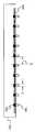
도 5a 내지 도 5c는 약하게 도핑된 영역(505)보다 더 높은 농도의 n-타입 불순물로 기판(500)을 도핑하여, 그리드라인(580A 내지 580C)을 형성하여, 죽은 층의 형성을 감소시키는 대안적인 방식을 도시한다. 도 5a에 도시된 실시예에서, 물리적인 마스크(515)는 광-수용 영역(505) 위에 위치된다. 이 마스크(515)는 요구된 그리드라인(580A)의 치수로 성형 된 개구부를 갖는다; 대안으로, 이 개구부는 알려진 양만큼, 그리드라인(580A)의 치수보다 약간 더 크다. 그런 후에, 이온 빔(600)은 마스크(515)에 유도되어, 이에 의해 그리드라인(580A)을 형성한다. 대안적인 실시예에서, 빔(600)은 플라즈마 빔이며, 기판(500)은 이 빔에 노출된다. 이 배열은 위에 서술된 바와 같이 빔 스캐닝 또는 빔 성형과 결합되어 사용될 수 있어서, 빔의 활용을 극대화한다.5A-5C illustrate an alternative to doping the
도 5b에서 도시된 실시예에서, 마스크(550)는 광-수용 영역(505) 상에 위치된다. 이 마스크(550)는 단단하거나 부드러울 수 있고, 리소그래피(lithography), 콘택트 프린팅(contact printing), 스크린 프린팅을 사용하여 형성될 수 있다. 대안으로, 콘택트 증착(deposition)을 위해 사용되는 이미 존재하는 마스크 또한 사용될 수 있다. 다시, 이온 빔(610)은 마스크 상에 유도되어, 이에 의해 그리드라인(580B)을 주입한다. 대안적인 실시예에서, 플라즈마 빔은 이온 빔(610) 대신에 사용된다.In the embodiment shown in FIG. 5B,
도 5c에 도시된 실시예에서, 주입 빔(620)은 기판(500)을 도핑하고, 그리드라인(580C)을 형성하기 위하여 성형된다. 이러한 배열은 동시 노출을 위하여 일련의 빔 세트(sets)를 사용할 수 있는데, 이 빔 세트는 기판(500)을 가로질러 새기는 단일 스캐닝 및 스테핑 빔 스폿을 사용한다. 대안으로, 넓은 및 좁은 빔은 하나 또는 임의의 개수의 그리드라인(580C)을 개별적으로 노출하기 위하여 사용될 수 있다.In the embodiment shown in FIG. 5C,
도 6은 작동 기능 및 밴드 갭이 금속/반도체 영역의 형성에 의해 조절되는 처리 단계 이후의 기판(500)을 도시한다. 도 6에 도시된 바와 같이, 금속종(700)은 콘택트 핑커 아래의 영역, 그리드라인(580)(580A 내지 580C 중 어느 하나)의 위에, 및 또한, 기판(500)(미도시)의 뒷면에 주입된다. 이러한 "시드" 주입은 금속 핑거(그리드 라인에 부착된) 및 로드에 콘택트 성능을 증가시킨다.6 shows the
도 6을 참조하면, 인접한 그리드라인(580) 사이의 도핑은 대략 100Ω/□이고, 그리드라인(580) 아래의 도핑은 10 내지 30Ω/□이며, 그리드 라인 사이의 거리(X)는 대략 3mm이지만, 1mm로 감소 될 것이라 예상되고, 그리고 금속종(금속 핑거)의 폭(Y)은 대략 200 미크론인데, 50미크론으로 감소될 것이라 예상된다.Referring to FIG. 6, the doping between
기판(500)은 성장한 단일의 또는 단(mono)-결정, 폴리(poly)-결정, 또는 다(multi) 결정 실리콘, 얇은-필름 증착 실리콘, 또는 솔라 셀을 형성하기 위하여 사용되는 임의의 다른 물질일 수 있다. 다른 타입의 기판 및 도핑이 사용될 수 있음을 인식할 것이다. 오직 하나의 예시로서, 기판(500)은 n-타입일 수 있고, 그리드라인(580A)은 p-타입일 수 있다. p-타입 불순물의 예시는 붕소 및 붕소 디플로라이드(diflouride)를 포함한다. 당업자라면, 반도체 타입, 이온, 레벨, 및 다른 특징의 다수의 다른 조합을 인지할 것이다.
도 7, 도 8, 도 9a, 및 도 9b는 본 발명의 실시예{예, 도 2의 시스템(200)}에 따라 어떻게 시스템이 죽은 층의 형성 및 저항 손실을 줄이기 위하여 도핑 프로파일을 맞춤화하는지를 도시하기 위하여 사용된다.7, 8, 9A, and 9B illustrate how the system customizes the doping profile to reduce dead layer formation and resistive loss in accordance with embodiments of the present invention (eg, the
도 7은 본 발명의 원리에 따른 프로파일 맞춤화 그래프(800)의 하나의 실시예를 도시한다. 그래프(800)는 불순물 깊이(Å) 대 불순물 농도(원자/cm3)에 대하여 솔라 셀의 원자 프로파일을 도시한다. 전체 원자의 프로파일은 선(810)에 의해 나타난다. 각각이 상이한 깊이 프로파일-대-농도를 갖는 다수의 이온 주입의 사용을 통하여, 솔라 셀의 불순물 농도(따라서, 고유 저항)는 정밀하게 조절될 수 있고, 사용자에 의해 사전 결정된 깊이를 가로질러 제어될 수 있다. 그래프(800)는 3가지 상이한 주입 프로파일(812, 814, 및 816)을 도시한다. 이들 3가지 프로파일의 조합은 솔라 셀의 전체 프로파일(810)을 초래한다.7 illustrates one embodiment of a
각 개별적인 주입이 가우시안(Gaussian) 또는 의사(pseudo)-가우시안 분포에 제한될 수 있지만, 본 발명은 전체 원자 프로파일의 성형을 효율적으로 맞춤화 하기 위하여 이들을 결합한다. 다수의 독립적인 주입의 사용을 통하여 전체 원자 프로파일의 제어에서, 본 발명은 사용자가 접합 깊이(840)를 효율적으로 제어할 수 있게 하고, 여기에서 하나의 타입의 주입된 불순물(예를 들어 n-타입 불순물)이 사전-도핑 된 바탕 영역(820)의 불순물(p-타입 불순물과 같은)을 충족시킨다. 또한, 사용자는 솔라 셀의 표면에서 또는 이 표면 근처에서 불순물 농도(830) 또한 제어할 수 있다. 본 발명은 사용자가 표면 농도(830) 및 접합 깊이(840)를 서로 독립적으로 제어하는 것을 허용한다. 일부 실시예에서, 원자 프로파일은 대략 0.01㎛ 내지 대략 0.5㎛의 범위의 접합 깊이를 갖기 위하여 맞춤화된다. 일부 실시예에서, 원자 프로파일은 대략 5 * 1018 원자/cm3 내지 대략 4.8 * 1021 원자/cm3의 범위로 표면 농도를 갖기 위하여 맞춤화된다. 하지만, 원자 프로파일이 상이한 접합 깊이 및 표면 농도를 갖기 위하여 맞춤화될 수 있다는 것을 고려할 수 있다.Although each individual injection can be limited to a Gaussian or pseudo-Gaussian distribution, the present invention combines them to efficiently customize the shaping of the entire atomic profile. In the control of the overall atomic profile through the use of multiple independent implants, the present invention allows the user to efficiently control the junction depth 840, where one type of implanted impurities (e.g. n- Type impurities) meet impurities (such as p-type impurities) of the pre-doped background region 820. The user can also control the impurity concentration 830 at or near the surface of the solar cell. The present invention allows the user to control the surface concentration 830 and the junction depth 840 independently of each other. In some embodiments, the atomic profile is customized to have a junction depth in the range of about 0.01 μm to about 0.5 μm. In some embodiments, the atomic profile is customized to have a surface concentration in the range of about 5 * 1018 atoms / cm3 to about 4.8 * 1021 atoms / cm3 . However, it is contemplated that the atomic profile can be customized to have different junction depths and surface concentrations.
종래 기술에서, 원자 프로파일의 조절은 제한된다. 도 8은 확산을 사용하여 도핑된 솔라 셀에 대한 프로파일 맞춤화 능력의 단점을 설명하는 그래프(900)이다. 여기에서, 선(910)은 솔라 셀에 대한 원자 프로파일을 나타낸다. 반도성 웨이퍼를 도핑하기 위한 확산의 사용은 사용자가 표면 농도 및 접합 깊이를 독립적으로 제어할 수 있는 것을 막는다. 사용자는 농도 및 깊이를 함께 선(910')으로 간단히 증가시킴으로써 프로파일(910)을 더 깊게 할 수 있거나, 또는 농도 및 깊이를 함께 선(910˝)으로 감소시킴으로써, 프로파일(910)을 더 얕게 하는데 제한된다. 사용자는 원자 프로파일의 형태를 변경할 수 없고, 또는 다른 것 이상으로 원자 프로파일에 대한 하나의 양상에 영향을 줄 수 없다.In the prior art, adjustment of the atomic profile is limited. 8 is a
도 9a 및 도 9b는 본 발명의 원리에 따라, 이온 주입을 사용하여 도핑된 솔라 셀에 대한 프로파일 맞춤화 능력의 장점을 도시하는 그래프이다. 도 9a의 그래프(1000)에서, 깊이-대-농도에 대한 원자 프로파일(1010)은 종래 기술의 방법을 사용하여 형성된 솔라 셀에 대하여 도시된다. 여기에서, 프로파일(1010)은 간단한 가우시안 분포로 제한되는데, 영역을 생성하는 전자-홀 쌍에 생성된 전자가 콘택트까지 이동하는 것을 어렵게 한다. 프로파일(1010)의 가파른 기울기는 전자가 웨이퍼 표면의 전도성 콘택트를 향해 이동할 때, 불순물 농도(따라서, 고유저항)의 상당한 증가를 반영한다. 프로파일(1010)의 가파른 경사는 전자가 전도성 콘택트에 도달하는 것을 어렵게 할 수 있어서, 전기의 원치않는 손실을 초래한다.9A and 9B are graphs illustrating the advantages of profile customization capabilities for solar cells doped using ion implantation, in accordance with the principles of the present invention. In the
도 9b의 그래프(1000')에서, 깊이-대-농도에 대한 원자 프로파일(1010')은 본 발명의 다수의 이온 주입을 사용하여 형성되는 솔라 셀에 대하여 도시된다. 프로파일(1010')은 농도의 더 점진적인(덜 가파른) 증가를 형성하기 위하여 성형 될 수 있는데, 이는 전자가 반도성 웨이퍼의 표면에서 콘택트 쪽으로 이동하기 때문이다. 이러한 원자 프로파일의 맞춤화는 접합 깊이 및 표면 농도뿐 아니라 이들 사이의 무엇이라도 독립적으로 제어하기 위하여, 다수의 이온 주입의 사용을 통하여 가능해질 수 있다.In the
도 7에서, 상이한 주입(812, 814, 및 816)은 솔라 셀의 상이한 양상을 결정할 수 있다. 예를 들어, 일부 실시예에서, 선(814 및 816)이 선택적 에미터 영역을 제공하기 위하여 일련의 선택적 주입으로서 추가되는 반면에, 선(812)(중간-범위 주입)은 균질한 에미터를 결정한다. 이들 주입 단계는 솔라 셀 제작을 위해 요구되는 표면 텍스쳐링(texturing) 뿐만이 아니라, 임의의 커버링 없이 블랭킷 방식으로 기판 상에 또는 임의의 반사-방지 커버링(예를 들어, 질소화물(nitride), 산화물(oxide), 또는 임의의 다른 필름)을 통하여 수행될 수 있다. 텍스쳐링의 경우, 이온 주입은 표면 윤곽에 좋은 부착을 제공하여, 콘택트 형성을 향상시킨다. 텍스쳐링은 미국 가출원 번호 61/133,028에 서술되며, 위에서 참조로 통합되었다. 도 7의 그래프(800)는 이전에 논의된 반사-방지 코팅과 같은 표면 코팅(850)을 도시한다. 이러한 코팅은 임의의 두께일 수 있다.In FIG. 7,
도 10은 실시예에 따라, 솔라 셀을 제작하기 위한 처리(1100)의 단계를 도시하는 흐름도이다. 도 2 및 도 10을 참조하면, 처리는 처리 애플리케이션(application)을 적합시키기 위하여 요구되는 특정 이온 소스(210)가 시스템(200)에 플러그 되는 단계(1101)를 시작한다. 단계(1103)에서, 단일 웨이퍼는 로드 락(230)에 위치된다. 단계(1105)에서, 웨이퍼는 하나의 농도 및 그리드라인을 형성하기 위한 더 높은 농도로 광-수용 영역을 도핑함으로써 처리된다. 이러한 단계는 다수의 도핑 싸이클을 포함할 수 있다.10 is a flowchart illustrating steps in a
그 다음에, 단계(1107)에서, 콘택트 시드, 프린트되거나 또는 잉크젯(inkjet)으로 프린트된 금속 핑거, 버스바 및 다른 콘택트가 형성된다. 단계(1109)에서, 웨이퍼는 콘택트를 확립하기 위하여 및 기판 도핑을 활성화하고 어닐링하기 위하여 웨이퍼가 가열될 수 있다. 웨이퍼는 오직 소수의 디바이스만으로 지정된 노, 플래쉬 램프, 또는 레이저를 사용하여, 종래 기술의 시스템을 사용할 시 요구되는 온도보다 낮은 400 내지 500℃의 온도로 어닐링될 수 있다. 바람직하게, 오직 단일 어닐링 단계만이 요구된다. 또한, 웨이퍼는 비교할만한 결과를 초래하는 시간 동안 상이한 온도로 어닐링 될 수 있다.Next, at
단계(1111)에서, 웨이퍼는 성능을 위해 측정되고, 그런 후에 분류된다. 이 처리는 단계(1113)에서 종료한다.In
바람직하게, 단계(1100)는 (1) 컴퓨터가-판독할 수 있는 매체 상에 저장된 컴퓨터가-실행할 수 있는 지령 및 (2) 이 지령을 실행하는 처리기에 의해 수행된다. 도 2를 참조하면, 하나의 실시예에서, 이러한 제어기(미도시)는 빔 스캐닝, 질량 분석 및 빔 성형 모듈(220) 및 측정 및 제어 모듈(225), 또는 이 두 모듈에 동작 가능하게 연결된다.Preferably,
실시예가 솔라 셀을 서술하지만, 이 실시예는 다른 반도체 디바이스가 실시예에 따라 제작될 수 있다는 것이 명백하다.Although the embodiment describes a solar cell, it is apparent that this embodiment can be fabricated in accordance with the embodiment.
당업자에게 있어서, 청구항에 의해 정의된 본 발명의 사상 및 범주로부터의 이탈 없이도 다른 변형이 실시예로 구현할 수 있다는 것은 이의 없이 명백할 것이다.It will be apparent to those skilled in the art that other modifications may be made to the embodiments without departing from the spirit and scope of the invention as defined by the claims.
100 : 주입 시스템101 : 웨이퍼(waper)
110 : 가스 전달 모듈105 : 트윈 로드 락(lock)
125 : 자석(magnet)130 : 후-가속 장치
135 : 전하 중화 모듈100
110: gas delivery module 105: twin rod lock
125: magnet 130: post-acceleration device
135: charge neutralization module
Claims (26)
Translated fromKorean이온(ion) 소스(source),
상기 이온 소스로부터 150kV 미만의 에너지를 갖는 빔을 생성하기 위한 가속 장치, 및
상기 기판을 상기 빔에 노출시키는 빔 디렉터(director)를
포함하는, 반도체 기판에 주입하기 위한 시스템.A system for implanting into a semiconductor substrate,
Ion source,
An accelerator for generating a beam having an energy of less than 150 kV from the ion source, and
A beam director that exposes the substrate to the beam.
And a system for implantation into a semiconductor substrate.
기판 내의 광(photo)-수용 영역을 제 1 농도로 도핑(doping)하는 단계,
그리드라인(gridlines)을 형성하기 위하여 제 1 농도 보다 높은 제 2 농도로 광-수용 영역을 도핑하는 단계로서, 상기 그리드라인은 상기 광-수용 영역의 가장 높은(topmost) 표면으로부터 상기 기판 내의 아래로 확장되는, 도핑 단계, 및
금속 핑거(finger)를 상기 그리드라인에 연결하는 단계를
포함하고, 상기 광-수용 영역 및 상기 그리드라인은 단일-종의 전달 모듈을 포함하는 시스템을 사용하여 도핑되는, 반도체 디바이스를 제작하기 위한 방법.In the method for manufacturing a semiconductor device,
Doping the photo-receptive region in the substrate to a first concentration,
Doping the light-receiving region at a second concentration higher than the first concentration to form gridlines, wherein the gridlines are from within the substrate from the topmost surface of the light-receiving region. Extended, doping step, and
Connecting a metal finger to the grid line
Wherein the light-receiving region and the gridline are doped using a system comprising a single-species transfer module.
150kV 미만의 에너지를 갖는 이온 빔을 사용하는 제 1 농도로 기판 내의 광-수용 영역을 도핑하는 단계,
그리드라인을 형성하기 위하여 상기 이온 빔을 사용하는 상기 제 1 농도보다 강한 제 2 농도로 상기 광-수용 영역을 도핑하는 단계로서, 상기 그리드라인은 상기 광-수용 영역의 가장 높은 포면으로부터 상기 기판 내의 아래로 확장되는, 도핑 단계, 및
금속 핑거를 상기 그리드라인에 연결하는 단계를
포함하고, 상기 기판은 156mm x 156mm이고, 상기 광 수용 영역은 단일-종의 전달 모듈을 포함하는 시스템을 사용하여 도핑되며, 상기 시스템의 처리량은 적어도 시간당 1,000개의 웨이퍼인, 솔라 셀을 제작하기 위한 방법.In the method for manufacturing a solar cell,
Doping the light-receiving region in the substrate at a first concentration using an ion beam having an energy of less than 150 kV,
Doping the light-receiving region to a second concentration stronger than the first concentration using the ion beam to form a grid line, wherein the grid line is in the substrate from the highest surface of the light-receiving region. A doping step that extends down, and
Connecting a metal finger to the grid line
Wherein the substrate is 156 mm by 156 mm and the light receiving region is doped using a system comprising a single-species transfer module, the throughput of the system being at least 1,000 wafers per hour. Way.
Applications Claiming Priority (10)
| Application Number | Priority Date | Filing Date | Title |
|---|---|---|---|
| US13168708P | 2008-06-11 | 2008-06-11 | |
| US13169808P | 2008-06-11 | 2008-06-11 | |
| US13168808P | 2008-06-11 | 2008-06-11 | |
| US61/131,698 | 2008-06-11 | ||
| US61/131,687 | 2008-06-11 | ||
| US61/131,688 | 2008-06-11 | ||
| US13302808P | 2008-06-24 | 2008-06-24 | |
| US61/133,028 | 2008-06-24 | ||
| US21054509P | 2009-03-20 | 2009-03-20 | |
| US61/210,545 | 2009-03-20 |
Publications (1)
| Publication Number | Publication Date |
|---|---|
| KR20110050423Atrue KR20110050423A (en) | 2011-05-13 |
Family
ID=41413647
Family Applications (4)
| Application Number | Title | Priority Date | Filing Date |
|---|---|---|---|
| KR1020117000467ACeasedKR20110042051A (en) | 2008-06-11 | 2009-06-11 | Fabrication of Solar Cells Using Injection |
| KR1020117000471AWithdrawnKR20110042052A (en) | 2008-06-11 | 2009-06-11 | Solar Cell Fabrication Using Passing and Ion Implantation |
| KR1020117000605AWithdrawnKR20110042053A (en) | 2008-06-11 | 2009-06-11 | Formation and annealing method of solar cell-selective emitter using injection |
| KR1020117000362AWithdrawnKR20110050423A (en) | 2008-06-11 | 2009-06-11 | Application-Specific Injection Systems and Methods for Use in Solar Cell Fabrication |
Family Applications Before (3)
| Application Number | Title | Priority Date | Filing Date |
|---|---|---|---|
| KR1020117000467ACeasedKR20110042051A (en) | 2008-06-11 | 2009-06-11 | Fabrication of Solar Cells Using Injection |
| KR1020117000471AWithdrawnKR20110042052A (en) | 2008-06-11 | 2009-06-11 | Solar Cell Fabrication Using Passing and Ion Implantation |
| KR1020117000605AWithdrawnKR20110042053A (en) | 2008-06-11 | 2009-06-11 | Formation and annealing method of solar cell-selective emitter using injection |
Country Status (6)
| Country | Link |
|---|---|
| US (4) | US20090308440A1 (en) |
| EP (4) | EP2304803A1 (en) |
| JP (4) | JP2011524639A (en) |
| KR (4) | KR20110042051A (en) |
| CN (4) | CN102150278A (en) |
| WO (4) | WO2009152368A1 (en) |
Cited By (2)
| Publication number | Priority date | Publication date | Assignee | Title |
|---|---|---|---|---|
| US9741894B2 (en) | 2009-06-23 | 2017-08-22 | Intevac, Inc. | Ion implant system having grid assembly |
| US9875922B2 (en) | 2011-11-08 | 2018-01-23 | Intevac, Inc. | Substrate processing system and method |
Families Citing this family (132)
| Publication number | Priority date | Publication date | Assignee | Title |
|---|---|---|---|---|
| US7442629B2 (en) | 2004-09-24 | 2008-10-28 | President & Fellows Of Harvard College | Femtosecond laser-induced formation of submicrometer spikes on a semiconductor substrate |
| US7057256B2 (en) | 2001-05-25 | 2006-06-06 | President & Fellows Of Harvard College | Silicon-based visible and near-infrared optoelectric devices |
| EP1988773B1 (en)* | 2006-02-28 | 2014-04-23 | Basf Se | Antimicrobial compounds |
| WO2007128142A1 (en)* | 2006-05-04 | 2007-11-15 | Elektrobit Wireless Communications Ltd. | Method for operating an rfid network |
| US20090317937A1 (en)* | 2008-06-20 | 2009-12-24 | Atul Gupta | Maskless Doping Technique for Solar Cells |
| US8461032B2 (en)* | 2008-03-05 | 2013-06-11 | Varian Semiconductor Equipment Associates, Inc. | Use of dopants with different diffusivities for solar cell manufacture |
| US20090239363A1 (en)* | 2008-03-24 | 2009-09-24 | Honeywell International, Inc. | Methods for forming doped regions in semiconductor substrates using non-contact printing processes and dopant-comprising inks for forming such doped regions using non-contact printing processes |
| CN102150278A (en)* | 2008-06-11 | 2011-08-10 | 因特瓦克公司 | Formation of solar cell-selective emitter using implant and anneal method |
| US8053867B2 (en) | 2008-08-20 | 2011-11-08 | Honeywell International Inc. | Phosphorous-comprising dopants and methods for forming phosphorous-doped regions in semiconductor substrates using phosphorous-comprising dopants |
| US7951696B2 (en) | 2008-09-30 | 2011-05-31 | Honeywell International Inc. | Methods for simultaneously forming N-type and P-type doped regions using non-contact printing processes |
| US8937244B2 (en) | 2008-10-23 | 2015-01-20 | Alta Devices, Inc. | Photovoltaic device |
| US8518170B2 (en) | 2008-12-29 | 2013-08-27 | Honeywell International Inc. | Boron-comprising inks for forming boron-doped regions in semiconductor substrates using non-contact printing processes and methods for fabricating such boron-comprising inks |
| US7820532B2 (en) | 2008-12-29 | 2010-10-26 | Honeywell International Inc. | Methods for simultaneously forming doped regions having different conductivity-determining type element profiles |
| JP5297840B2 (en)* | 2009-03-03 | 2013-09-25 | シャープ株式会社 | LAMINATE, THIN-FILM PHOTOELECTRIC CONVERSION DEVICE, INTEGRATED THIN-FILM SOLAR CELL AND METHOD FOR PRODUCING THEM |
| US9076914B2 (en) | 2009-04-08 | 2015-07-07 | Varian Semiconductor Equipment Associates, Inc. | Techniques for processing a substrate |
| US9006688B2 (en)* | 2009-04-08 | 2015-04-14 | Varian Semiconductor Equipment Associates, Inc. | Techniques for processing a substrate using a mask |
| US8900982B2 (en)* | 2009-04-08 | 2014-12-02 | Varian Semiconductor Equipment Associates, Inc. | Techniques for processing a substrate |
| US8330128B2 (en)* | 2009-04-17 | 2012-12-11 | Varian Semiconductor Equipment Associates, Inc. | Implant mask with moveable hinged mask segments |
| US9318644B2 (en) | 2009-05-05 | 2016-04-19 | Solexel, Inc. | Ion implantation and annealing for thin film crystalline solar cells |
| US20110027463A1 (en)* | 2009-06-16 | 2011-02-03 | Varian Semiconductor Equipment Associates, Inc. | Workpiece handling system |
| TW201104822A (en)* | 2009-07-20 | 2011-02-01 | E Ton Solar Tech Co Ltd | Aligning method of patterned electrode in a selective emitter structure |
| US8324089B2 (en) | 2009-07-23 | 2012-12-04 | Honeywell International Inc. | Compositions for forming doped regions in semiconductor substrates, methods for fabricating such compositions, and methods for forming doped regions using such compositions |
| US8008176B2 (en)* | 2009-08-11 | 2011-08-30 | Varian Semiconductor Equipment Associates, Inc. | Masked ion implant with fast-slow scan |
| US9911781B2 (en) | 2009-09-17 | 2018-03-06 | Sionyx, Llc | Photosensitive imaging devices and associated methods |
| US9673243B2 (en) | 2009-09-17 | 2017-06-06 | Sionyx, Llc | Photosensitive imaging devices and associated methods |
| US9691921B2 (en) | 2009-10-14 | 2017-06-27 | Alta Devices, Inc. | Textured metallic back reflector |
| US9136422B1 (en) | 2012-01-19 | 2015-09-15 | Alta Devices, Inc. | Texturing a layer in an optoelectronic device for improved angle randomization of light |
| US20170141256A1 (en) | 2009-10-23 | 2017-05-18 | Alta Devices, Inc. | Multi-junction optoelectronic device with group iv semiconductor as a bottom junction |
| US11271128B2 (en) | 2009-10-23 | 2022-03-08 | Utica Leaseco, Llc | Multi-junction optoelectronic device |
| US20150380576A1 (en) | 2010-10-13 | 2015-12-31 | Alta Devices, Inc. | Optoelectronic device with dielectric layer and method of manufacture |
| US9502594B2 (en)* | 2012-01-19 | 2016-11-22 | Alta Devices, Inc. | Thin-film semiconductor optoelectronic device with textured front and/or back surface prepared from template layer and etching |
| US9768329B1 (en) | 2009-10-23 | 2017-09-19 | Alta Devices, Inc. | Multi-junction optoelectronic device |
| US9012766B2 (en) | 2009-11-12 | 2015-04-21 | Silevo, Inc. | Aluminum grid as backside conductor on epitaxial silicon thin film solar cells |
| US8461030B2 (en) | 2009-11-17 | 2013-06-11 | Varian Semiconductor Equipment Associates, Inc. | Apparatus and method for controllably implanting workpieces |
| KR20110089497A (en)* | 2010-02-01 | 2011-08-09 | 삼성전자주식회사 | Impurity doping method on substrate, manufacturing method of solar cell using same and solar cell manufactured using same |
| US8735234B2 (en)* | 2010-02-18 | 2014-05-27 | Varian Semiconductor Equipment Associates, Inc. | Self-aligned ion implantation for IBC solar cells |
| US8921149B2 (en)* | 2010-03-04 | 2014-12-30 | Varian Semiconductor Equipment Associates, Inc. | Aligning successive implants with a soft mask |
| US8912082B2 (en)* | 2010-03-25 | 2014-12-16 | Varian Semiconductor Equipment Associates, Inc. | Implant alignment through a mask |
| TW201133905A (en)* | 2010-03-30 | 2011-10-01 | E Ton Solar Tech Co Ltd | Method of forming solar cell |
| US8084293B2 (en) | 2010-04-06 | 2011-12-27 | Varian Semiconductor Equipment Associates, Inc. | Continuously optimized solar cell metallization design through feed-forward process |
| JP2011228360A (en)* | 2010-04-15 | 2011-11-10 | Institute Of Physical & Chemical Research | Solar cell |
| US8692198B2 (en) | 2010-04-21 | 2014-04-08 | Sionyx, Inc. | Photosensitive imaging devices and associated methods |
| US20120111396A1 (en)* | 2010-05-04 | 2012-05-10 | Sionyx, Inc. | Photovoltaic Devices and Associated Methods |
| CN101866971A (en)* | 2010-05-18 | 2010-10-20 | 常州亿晶光电科技有限公司 | Broken solar cells with selective emitting stage |
| TWI399863B (en)* | 2010-05-26 | 2013-06-21 | Inventec Solar Energy Corp | Rapid thermal annealing apparatus for selective heat treatment and method for selective emitter solar cell fabrication using the same |
| US8071418B2 (en)* | 2010-06-03 | 2011-12-06 | Suniva, Inc. | Selective emitter solar cells formed by a hybrid diffusion and ion implantation process |
| US8110431B2 (en)* | 2010-06-03 | 2012-02-07 | Suniva, Inc. | Ion implanted selective emitter solar cells with in situ surface passivation |
| US9214576B2 (en) | 2010-06-09 | 2015-12-15 | Solarcity Corporation | Transparent conducting oxide for photovoltaic devices |
| WO2011158514A1 (en) | 2010-06-17 | 2011-12-22 | パナソニック株式会社 | Polycrystalline-type solar cell panel and process for production thereof |
| WO2011160130A2 (en) | 2010-06-18 | 2011-12-22 | Sionyx, Inc | High speed photosensitive devices and associated methods |
| US8563351B2 (en) | 2010-06-25 | 2013-10-22 | Taiwan Semiconductor Manufacturing Co., Ltd. | Method for manufacturing photovoltaic device |
| US8293645B2 (en) | 2010-06-30 | 2012-10-23 | Taiwan Semiconductor Manufacturing Co., Ltd. | Method for forming photovoltaic cell |
| US8664100B2 (en)* | 2010-07-07 | 2014-03-04 | Varian Semiconductor Equipment Associates, Inc. | Manufacturing high efficiency solar cell with directional doping |
| CN102376789A (en)* | 2010-08-24 | 2012-03-14 | 中芯国际集成电路制造(上海)有限公司 | Selective emitter solar battery and preparation method |
| US20110139231A1 (en)* | 2010-08-25 | 2011-06-16 | Daniel Meier | Back junction solar cell with selective front surface field |
| US9773928B2 (en) | 2010-09-10 | 2017-09-26 | Tesla, Inc. | Solar cell with electroplated metal grid |
| US9800053B2 (en) | 2010-10-08 | 2017-10-24 | Tesla, Inc. | Solar panels with integrated cell-level MPPT devices |
| TWI431797B (en)* | 2010-10-19 | 2014-03-21 | Ind Tech Res Inst | Selective emitter solar cell and manufacturing method thereof |
| US9231061B2 (en) | 2010-10-25 | 2016-01-05 | The Research Foundation Of State University Of New York | Fabrication of surface textures by ion implantation for antireflection of silicon crystals |
| TWI469368B (en)* | 2010-11-17 | 2015-01-11 | Intevac Inc | Direct current ion implantation for solid epitaxial growth in solar cell manufacturing |
| TWI488321B (en)* | 2010-12-10 | 2015-06-11 | Teijin Ltd | Semiconductor laminates, semiconductor devices, and the like |
| EP2490268A1 (en)* | 2011-02-03 | 2012-08-22 | Imec | Method for fabricating photovoltaic cells |
| JP2014512673A (en)* | 2011-03-08 | 2014-05-22 | アライアンス フォー サステイナブル エナジー リミテッド ライアビリティ カンパニー | Efficient black silicon photovoltaic device with improved blue sensitivity |
| JP5496136B2 (en)* | 2011-03-25 | 2014-05-21 | 三菱電機株式会社 | Photovoltaic device and photovoltaic module |
| WO2012140808A1 (en)* | 2011-04-15 | 2012-10-18 | 三菱電機株式会社 | Solar cell and manufacturing method for same, and solar cell module |
| TWI424582B (en)* | 2011-04-15 | 2014-01-21 | Au Optronics Corp | Solar cell manufacturing method |
| EP2715797A4 (en)* | 2011-05-27 | 2015-05-27 | Solexel Inc | ION IMPLANTATION AND ANNEALING FOR HIGH EFFICIENCY SOLAR CELLS WITH REAR JUNCTION AND REAR CONTACT |
| US9054256B2 (en) | 2011-06-02 | 2015-06-09 | Solarcity Corporation | Tunneling-junction solar cell with copper grid for concentrated photovoltaic application |
| US9496308B2 (en) | 2011-06-09 | 2016-11-15 | Sionyx, Llc | Process module for increasing the response of backside illuminated photosensitive imagers and associated methods |
| US8697559B2 (en)* | 2011-07-07 | 2014-04-15 | Varian Semiconductor Equipment Associates, Inc. | Use of ion beam tails to manufacture a workpiece |
| WO2013010127A2 (en) | 2011-07-13 | 2013-01-17 | Sionyx, Inc. | Biometric imaging devices and associated methods |
| US8778448B2 (en)* | 2011-07-21 | 2014-07-15 | International Business Machines Corporation | Method of stabilizing hydrogenated amorphous silicon and amorphous hydrogenated silicon alloys |
| JP5726308B2 (en)* | 2011-07-28 | 2015-05-27 | 京セラ株式会社 | Solar cell element and solar cell module |
| US8629294B2 (en) | 2011-08-25 | 2014-01-14 | Honeywell International Inc. | Borate esters, boron-comprising dopants, and methods of fabricating boron-comprising dopants |
| CN102969214B (en)* | 2011-08-31 | 2017-08-25 | 圆益Ips股份有限公司 | Substrate board treatment and the base plate processing system with it |
| US8975170B2 (en) | 2011-10-24 | 2015-03-10 | Honeywell International Inc. | Dopant ink compositions for forming doped regions in semiconductor substrates, and methods for fabricating dopant ink compositions |
| US8507298B2 (en) | 2011-12-02 | 2013-08-13 | Varian Semiconductor Equipment Associates, Inc. | Patterned implant of a dielectric layer |
| KR101902887B1 (en)* | 2011-12-23 | 2018-10-01 | 엘지전자 주식회사 | Method for manufacturing the same |
| CN103199146A (en)* | 2012-01-04 | 2013-07-10 | 茂迪股份有限公司 | Solar cell manufacturing method |
| US11038080B2 (en) | 2012-01-19 | 2021-06-15 | Utica Leaseco, Llc | Thin-film semiconductor optoelectronic device with textured front and/or back surface prepared from etching |
| KR102044464B1 (en)* | 2012-01-30 | 2019-11-13 | 엘지전자 주식회사 | Solar cell and method for manufacturing the same |
| US20130199604A1 (en)* | 2012-02-06 | 2013-08-08 | Silicon Solar Solutions | Solar cells and methods of fabrication thereof |
| KR101807791B1 (en) | 2012-03-05 | 2018-01-18 | 엘지전자 주식회사 | Method for manufacturing solar cell |
| US9064764B2 (en) | 2012-03-22 | 2015-06-23 | Sionyx, Inc. | Pixel isolation elements, devices, and associated methods |
| US9099578B2 (en) | 2012-06-04 | 2015-08-04 | Nusola, Inc. | Structure for creating ohmic contact in semiconductor devices and methods for manufacture |
| WO2013152054A1 (en)* | 2012-04-02 | 2013-10-10 | Nusola Inc. | Photovoltaic cell and process of manufacture |
| US20130255774A1 (en)* | 2012-04-02 | 2013-10-03 | Nusola, Inc. | Photovoltaic cell and process of manufacture |
| JP2015519729A (en)* | 2012-04-02 | 2015-07-09 | ヌソラ インコーポレイテッドnusola Inc. | Photoelectric conversion element and manufacturing method thereof |
| US9412895B2 (en) | 2012-04-04 | 2016-08-09 | Samsung Sdi Co., Ltd. | Method of manufacturing photoelectric device |
| US8895325B2 (en)* | 2012-04-27 | 2014-11-25 | Varian Semiconductor Equipment Associates, Inc. | System and method for aligning substrates for multiple implants |
| KR101879781B1 (en)* | 2012-05-11 | 2018-08-16 | 엘지전자 주식회사 | Solar cell, method for manufacturing dopant layer, and method for manufacturing solar cell |
| US9865754B2 (en) | 2012-10-10 | 2018-01-09 | Tesla, Inc. | Hole collectors for silicon photovoltaic cells |
| MY178951A (en)* | 2012-12-19 | 2020-10-23 | Intevac Inc | Grid for plasma ion implant |
| US9530923B2 (en)* | 2012-12-21 | 2016-12-27 | Sunpower Corporation | Ion implantation of dopants for forming spatially located diffusion regions of solar cells |
| US9219174B2 (en) | 2013-01-11 | 2015-12-22 | Solarcity Corporation | Module fabrication of solar cells with low resistivity electrodes |
| US9412884B2 (en) | 2013-01-11 | 2016-08-09 | Solarcity Corporation | Module fabrication of solar cells with low resistivity electrodes |
| US10074755B2 (en) | 2013-01-11 | 2018-09-11 | Tesla, Inc. | High efficiency solar panel |
| US9762830B2 (en) | 2013-02-15 | 2017-09-12 | Sionyx, Llc | High dynamic range CMOS image sensor having anti-blooming properties and associated methods |
| US9029049B2 (en)* | 2013-02-20 | 2015-05-12 | Infineon Technologies Ag | Method for processing a carrier, a carrier, an electronic device and a lithographic mask |
| WO2014151093A1 (en) | 2013-03-15 | 2014-09-25 | Sionyx, Inc. | Three dimensional imaging utilizing stacked imager devices and associated methods |
| FR3003687B1 (en)* | 2013-03-20 | 2015-07-17 | Mpo Energy | METHOD FOR DOPING SILICON PLATES |
| CN104078519A (en)* | 2013-03-28 | 2014-10-01 | 比亚迪股份有限公司 | Solar cell slice and fabrication method thereof |
| CN103268905B (en)* | 2013-05-17 | 2017-02-08 | 浙江正泰太阳能科技有限公司 | Manufacturing method of solar crystalline silicon battery |
| CN103280489B (en)* | 2013-05-17 | 2016-02-03 | 浙江正泰太阳能科技有限公司 | A kind of method realizing selective emitter |
| US9209345B2 (en) | 2013-06-29 | 2015-12-08 | Sionyx, Inc. | Shallow trench textured regions and associated methods |
| FR3010227B1 (en)* | 2013-09-04 | 2015-10-02 | Commissariat Energie Atomique | PROCESS FOR FORMATION OF A PHOTOVOLTAIC CELL |
| US9577134B2 (en)* | 2013-12-09 | 2017-02-21 | Sunpower Corporation | Solar cell emitter region fabrication using self-aligned implant and cap |
| US9960287B2 (en) | 2014-02-11 | 2018-05-01 | Picasolar, Inc. | Solar cells and methods of fabrication thereof |
| FR3018391B1 (en)* | 2014-03-07 | 2016-04-01 | Commissariat Energie Atomique | METHOD FOR MAKING A SELECTIVE DOPING PHOTOVOLTAIC CELL |
| US9337369B2 (en) | 2014-03-28 | 2016-05-10 | Sunpower Corporation | Solar cells with tunnel dielectrics |
| US10309012B2 (en) | 2014-07-03 | 2019-06-04 | Tesla, Inc. | Wafer carrier for reducing contamination from carbon particles and outgassing |
| US9343312B2 (en)* | 2014-07-25 | 2016-05-17 | Taiwan Semiconductor Manufacturing Company, Ltd. | High temperature intermittent ion implantation |
| CN105489489B (en)* | 2014-10-09 | 2019-03-15 | 江苏中科君芯科技有限公司 | Production method, the production method of TI-IGBT of semiconductor devices |
| US9899546B2 (en) | 2014-12-05 | 2018-02-20 | Tesla, Inc. | Photovoltaic cells with electrodes adapted to house conductive paste |
| US9947822B2 (en) | 2015-02-02 | 2018-04-17 | Tesla, Inc. | Bifacial photovoltaic module using heterojunction solar cells |
| US20160284913A1 (en)* | 2015-03-27 | 2016-09-29 | Staffan WESTERBERG | Solar cell emitter region fabrication using substrate-level ion implantation |
| CN105070789B (en)* | 2015-08-20 | 2017-11-10 | 苏州阿特斯阳光电力科技有限公司 | A kind of preparation method of crystal silicon solar energy battery emitter stage |
| US9761744B2 (en) | 2015-10-22 | 2017-09-12 | Tesla, Inc. | System and method for manufacturing photovoltaic structures with a metal seed layer |
| US9842956B2 (en) | 2015-12-21 | 2017-12-12 | Tesla, Inc. | System and method for mass-production of high-efficiency photovoltaic structures |
| US10115838B2 (en) | 2016-04-19 | 2018-10-30 | Tesla, Inc. | Photovoltaic structures with interlocking busbars |
| CN105845776A (en)* | 2016-04-26 | 2016-08-10 | 泰州中来光电科技有限公司 | Local back surface N-type photovoltaic cell preparation method, local back surface N-type photovoltaic cell, local back surface N-type photovoltaic cell assembly and local back surface N-type photovoltaic cell system |
| US11018225B2 (en) | 2016-06-28 | 2021-05-25 | International Business Machines Corporation | III-V extension by high temperature plasma doping |
| US10672919B2 (en) | 2017-09-19 | 2020-06-02 | Tesla, Inc. | Moisture-resistant solar cells for solar roof tiles |
| KR101833936B1 (en) | 2017-11-24 | 2018-03-02 | 엘지전자 주식회사 | Solar cell and method for manufacturing the same |
| US11190128B2 (en) | 2018-02-27 | 2021-11-30 | Tesla, Inc. | Parallel-connected solar roof tile modules |
| US10796899B2 (en)* | 2018-12-28 | 2020-10-06 | Micron Technology, Inc. | Silicon doping for laser splash blockage |
| CN110098283A (en)* | 2019-04-25 | 2019-08-06 | 晶科能源科技(海宁)有限公司 | A kind of ion implanting phosphorus diffusion method of matching laser selective doping |
| JP7645138B2 (en)* | 2021-06-17 | 2025-03-13 | 株式会社アルバック | Method for manufacturing hard mask and method for manufacturing solar cell |
| CN114256363A (en)* | 2021-09-23 | 2022-03-29 | 天合光能股份有限公司 | Suede structure of solar cell and preparation method |
| KR102676355B1 (en)* | 2021-12-22 | 2024-06-19 | 재단법인 구미전자정보기술원 | Line scanner using ultraviolet sensor based on single crystal silicon and manufacturing method thereof |
| CN117238977B (en) | 2023-11-15 | 2024-02-27 | 天合光能股份有限公司 | Solar cells and manufacturing methods, photovoltaic modules and photovoltaic systems |
| CN117316759B (en)* | 2023-11-28 | 2024-02-20 | 武汉鑫威源电子科技有限公司 | Method and device for improving doping efficiency of p-type gallium nitride |
Family Cites Families (327)
| Publication number | Priority date | Publication date | Assignee | Title |
|---|---|---|---|---|
| US554854A (en)* | 1896-02-18 | John f | ||
| US3786359A (en)* | 1969-03-28 | 1974-01-15 | Alpha Ind Inc | Ion accelerator and ion species selector |
| US3607450A (en)* | 1969-09-26 | 1971-09-21 | Us Air Force | Lead sulfide ion implantation mask |
| US3790412A (en)* | 1972-04-07 | 1974-02-05 | Bell Telephone Labor Inc | Method of reducing the effects of particle impingement on shadow masks |
| US3969746A (en) | 1973-12-10 | 1976-07-13 | Texas Instruments Incorporated | Vertical multijunction solar cell |
| US3969163A (en)* | 1974-09-19 | 1976-07-13 | Texas Instruments Incorporated | Vapor deposition method of forming low cost semiconductor solar cells including reconstitution of the reacted gases |
| US3948682A (en)* | 1974-10-31 | 1976-04-06 | Ninel Mineevna Bordina | Semiconductor photoelectric generator |
| US3976508A (en)* | 1974-11-01 | 1976-08-24 | Mobil Tyco Solar Energy Corporation | Tubular solar cell devices |
| JPS5165774U (en)* | 1974-11-20 | 1976-05-24 | ||
| US4144094A (en) | 1975-01-06 | 1979-03-13 | Motorola, Inc. | Radiation responsive current generating cell and method of forming same |
| US4004949A (en)* | 1975-01-06 | 1977-01-25 | Motorola, Inc. | Method of making silicon solar cells |
| US4072541A (en)* | 1975-11-21 | 1978-02-07 | Communications Satellite Corporation | Radiation hardened P-I-N and N-I-P solar cells |
| US4152536A (en) | 1975-12-05 | 1979-05-01 | Mobil Tyco Solar Energy Corp. | Solar cells |
| US4095329A (en) | 1975-12-05 | 1978-06-20 | Mobil Tyco Soalar Energy Corporation | Manufacture of semiconductor ribbon and solar cells |
| US4021276A (en)* | 1975-12-29 | 1977-05-03 | Western Electric Company, Inc. | Method of making rib-structure shadow mask for ion implantation |
| US4131488A (en) | 1975-12-31 | 1978-12-26 | Motorola, Inc. | Method of semiconductor solar energy device fabrication |
| US4070689A (en)* | 1975-12-31 | 1978-01-24 | Motorola Inc. | Semiconductor solar energy device |
| US4001864A (en)* | 1976-01-30 | 1977-01-04 | Gibbons James F | Semiconductor p-n junction solar cell and method of manufacture |
| US4056404A (en) | 1976-03-29 | 1977-11-01 | Mobil Tyco Solar Energy Corporation | Flat tubular solar cells and method of producing same |
| US4090213A (en)* | 1976-06-15 | 1978-05-16 | California Institute Of Technology | Induced junction solar cell and method of fabrication |
| US4116717A (en) | 1976-12-08 | 1978-09-26 | The United States Of America As Represented By The Secretary Of The Air Force | Ion implanted eutectic gallium arsenide solar cell |
| US4070205A (en)* | 1976-12-08 | 1978-01-24 | The United States Of America As Represented By The Secretary Of The Air Force | Aluminum arsenide eutectic gallium arsenide solar cell |
| US4086102A (en) | 1976-12-13 | 1978-04-25 | King William J | Inexpensive solar cell and method therefor |
| US4179311A (en)* | 1977-01-17 | 1979-12-18 | Mostek Corporation | Method of stabilizing semiconductor device by converting doped poly-Si to polyoxides |
| US4131486A (en) | 1977-01-19 | 1978-12-26 | The United States Of America As Represented By The Administrator Of The National Aeronautics And Space Administration | Back wall solar cell |
| US4141756A (en)* | 1977-10-14 | 1979-02-27 | Honeywell Inc. | Method of making a gap UV photodiode by multiple ion-implantations |
| US4152824A (en)* | 1977-12-30 | 1979-05-08 | Mobil Tyco Solar Energy Corporation | Manufacture of solar cells |
| US4301592A (en) | 1978-05-26 | 1981-11-24 | Hung Chang Lin | Method of fabricating semiconductor junction device employing separate metallization |
| US4219830A (en) | 1978-06-19 | 1980-08-26 | Gibbons James F | Semiconductor solar cell |
| US4253881A (en) | 1978-10-23 | 1981-03-03 | Rudolf Hezel | Solar cells composed of semiconductive materials |
| US4227941A (en) | 1979-03-21 | 1980-10-14 | Massachusetts Institute Of Technology | Shallow-homojunction solar cells |
| US4273950A (en) | 1979-05-29 | 1981-06-16 | Photowatt International, Inc. | Solar cell and fabrication thereof using microwaves |
| DE2941908C2 (en) | 1979-10-17 | 1986-07-03 | Licentia Patent-Verwaltungs-Gmbh, 6000 Frankfurt | Method for producing a solar cell having a silicon layer |
| US4490573A (en) | 1979-12-26 | 1984-12-25 | Sera Solar Corporation | Solar cells |
| DK79780A (en)* | 1980-02-25 | 1981-08-26 | Elektronikcentralen | Solar cells with a semiconductor crystal and with a lighted surface battery of solar cells and methods for making the same |
| JPS5713777A (en) | 1980-06-30 | 1982-01-23 | Shunpei Yamazaki | Semiconductor device and manufacture thereof |
| USRE31151E (en) | 1980-04-07 | 1983-02-15 | Inexpensive solar cell and method therefor | |
| US4295002A (en) | 1980-06-23 | 1981-10-13 | International Business Machines Corporation | Heterojunction V-groove multijunction solar cell |
| US4322571A (en)* | 1980-07-17 | 1982-03-30 | The Boeing Company | Solar cells and methods for manufacture thereof |
| DE3135933A1 (en) | 1980-09-26 | 1982-05-19 | Unisearch Ltd., Kensington, New South Wales | SOLAR CELL AND METHOD FOR THEIR PRODUCTION |
| US4421577A (en) | 1980-11-10 | 1983-12-20 | The Board Of Trustees Of The Leland Stanford, Junior University | Method for making Schottky barrier diodes with engineered heights |
| US4353160A (en) | 1980-11-24 | 1982-10-12 | Spire Corporation | Solar cell junction processing system |
| DE3049376A1 (en)* | 1980-12-29 | 1982-07-29 | Heliotronic Forschungs- und Entwicklungsgesellschaft für Solarzellen-Grundstoffe mbH, 8263 Burghausen | METHOD FOR PRODUCING VERTICAL PN TRANSITIONS WHEN DRAWING SILICO DISC FROM A SILICONE MELT |
| US4379944A (en) | 1981-02-05 | 1983-04-12 | Varian Associates, Inc. | Grooved solar cell for deployment at set angle |
| JPS57132373A (en)* | 1981-02-10 | 1982-08-16 | Agency Of Ind Science & Technol | Manufacture of solar battery |
| EP0078336B1 (en) | 1981-10-30 | 1988-02-03 | Ibm Deutschland Gmbh | Shadow projecting mask for ion implantation and lithography by ion beam radiation |
| JPS58164134A (en)* | 1982-03-24 | 1983-09-29 | Hitachi Ltd | Manufacturing method of semiconductor device |
| DE3234678A1 (en) | 1982-09-18 | 1984-04-05 | Battelle-Institut E.V., 6000 Frankfurt | SOLAR CELL |
| US4479027A (en) | 1982-09-24 | 1984-10-23 | Todorof William J | Multi-layer thin-film, flexible silicon alloy photovoltaic cell |
| US4456489A (en) | 1982-10-15 | 1984-06-26 | Motorola, Inc. | Method of forming a shallow and high conductivity boron doped layer in silicon |
| US4587430A (en) | 1983-02-10 | 1986-05-06 | Mission Research Corporation | Ion implantation source and device |
| DE3308269A1 (en) | 1983-03-09 | 1984-09-13 | Licentia Patent-Verwaltungs-Gmbh | SOLAR CELL |
| US4539431A (en) | 1983-06-06 | 1985-09-03 | Sera Solar Corporation | Pulse anneal method for solar cell |
| US4847504A (en)* | 1983-08-15 | 1989-07-11 | Applied Materials, Inc. | Apparatus and methods for ion implantation |
| US4522657A (en)* | 1983-10-20 | 1985-06-11 | Westinghouse Electric Corp. | Low temperature process for annealing shallow implanted N+/P junctions |
| US4589191A (en) | 1983-10-20 | 1986-05-20 | Unisearch Limited | Manufacture of high efficiency solar cells |
| US4524237A (en) | 1984-02-08 | 1985-06-18 | The United States Of America As Represented By The Administrator Of The National Aeronautics And Space Administration | Increased voltage photovoltaic cell |
| US4542256A (en) | 1984-04-27 | 1985-09-17 | University Of Delaware | Graded affinity photovoltaic cell |
| JPH0630237B2 (en) | 1984-09-10 | 1994-04-20 | 株式会社日立製作所 | Ion implanter |
| GB8423558D0 (en) | 1984-09-18 | 1984-10-24 | Secr Defence | Semi-conductor solar cells |
| US4667060A (en)* | 1985-05-28 | 1987-05-19 | Spire Corporation | Back junction photovoltaic solar cell |
| JPS61294866A (en)* | 1985-06-21 | 1986-12-25 | Nippon Texas Instr Kk | Charge-coupled type semiconductor device |
| JPS6215864A (en)* | 1985-07-15 | 1987-01-24 | Hitachi Ltd | How to manufacture solar cells |
| DE3536299A1 (en)* | 1985-10-11 | 1987-04-16 | Nukem Gmbh | SOLAR CELL MADE OF SILICON |
| US4676845A (en) | 1986-02-18 | 1987-06-30 | Spire Corporation | Passivated deep p/n junction |
| US4665277A (en)* | 1986-03-11 | 1987-05-12 | The United States Of America As Represented By The Administrator Of The National Aeronautics And Space Administration | Floating emitter solar cell |
| US4719355A (en)* | 1986-04-10 | 1988-01-12 | Texas Instruments Incorporated | Ion source for an ion implanter |
| US4737688A (en)* | 1986-07-22 | 1988-04-12 | Applied Electron Corporation | Wide area source of multiply ionized atomic or molecular species |
| JPS63143876A (en) | 1986-12-08 | 1988-06-16 | Hitachi Ltd | Manufacture of solar cell |
| DE3712503A1 (en) | 1987-04-13 | 1988-11-03 | Nukem Gmbh | SOLAR CELL |
| US4830678A (en)* | 1987-06-01 | 1989-05-16 | Todorof William J | Liquid-cooled sealed enclosure for concentrator solar cell and secondary lens |
| US4834805A (en)* | 1987-09-24 | 1989-05-30 | Wattsun, Inc. | Photovoltaic power modules and methods for making same |
| JPH01290267A (en)* | 1988-05-18 | 1989-11-22 | Fuji Electric Co Ltd | Manufacturing method of photoelectric conversion element |
| DE68923061T2 (en) | 1988-11-16 | 1995-11-09 | Mitsubishi Electric Corp | Solar cell. |
| JP2808004B2 (en)* | 1989-01-30 | 1998-10-08 | 京セラ株式会社 | Solar cell |
| US5132544A (en) | 1990-08-29 | 1992-07-21 | Nissin Electric Company Ltd. | System for irradiating a surface with atomic and molecular ions using two dimensional magnetic scanning |
| JP2875892B2 (en)* | 1990-12-20 | 1999-03-31 | 三菱重工業株式会社 | Method of forming cubic boron nitride film |
| US5112409A (en) | 1991-01-23 | 1992-05-12 | Solarex Corporation | Solar cells with reduced recombination under grid lines, and method of manufacturing same |
| US5125983A (en)* | 1991-04-22 | 1992-06-30 | Electric Power Research Institute, Inc. | Generating electric power from solar radiation |
| US5113735A (en)* | 1991-04-23 | 1992-05-19 | Alcan International Limited | Slitting apparatus |
| USH1637H (en)* | 1991-09-18 | 1997-03-04 | Offord; Bruce W. | Laser-assisted fabrication of bipolar transistors in silicon-on-sapphire (SOS) |
| JPH0797653B2 (en)* | 1991-10-01 | 1995-10-18 | 工業技術院長 | Photoelectric conversion element |
| JP2837296B2 (en) | 1991-10-17 | 1998-12-14 | シャープ株式会社 | Solar cell |
| DE4217428A1 (en)* | 1991-12-09 | 1993-06-17 | Deutsche Aerospace | High performance silicon crystalline solar cell structure - has more highly doped layer integrated in lightly doped layer in area below metallic contact |
| US5356488A (en) | 1991-12-27 | 1994-10-18 | Rudolf Hezel | Solar cell and method for its manufacture |
| DE4202455C1 (en) | 1992-01-29 | 1993-08-19 | Siemens Ag, 8000 Muenchen, De | |
| TW232079B (en)* | 1992-03-17 | 1994-10-11 | Wisconsin Alumni Res Found | |
| US5374456A (en) | 1992-12-23 | 1994-12-20 | Hughes Aircraft Company | Surface potential control in plasma processing of materials |
| US6084175A (en) | 1993-05-20 | 2000-07-04 | Amoco/Enron Solar | Front contact trenches for polycrystalline photovoltaic devices and semi-conductor devices with buried contacts |
| US5421889A (en) | 1993-06-29 | 1995-06-06 | Tokyo Electron Limited | Method and apparatus for inverting samples in a process |
| JP3159583B2 (en)* | 1993-11-10 | 2001-04-23 | シャープ株式会社 | Solar cell and method of manufacturing the same |
| KR100366910B1 (en)* | 1994-04-05 | 2003-03-04 | 소니 가부시끼 가이샤 | Manufacturing method of semiconductor device |
| FR2722612B1 (en) | 1994-07-13 | 1997-01-03 | Centre Nat Rech Scient | METHOD FOR MANUFACTURING A PHOTOVOLTAIC MATERIAL OR DEVICE, MATERIAL OR DEVICE THUS OBTAINED AND PHOTOPILE COMPRISING SUCH A MATERIAL OR DEVICE |
| US5583368A (en) | 1994-08-11 | 1996-12-10 | International Business Machines Corporation | Stacked devices |
| US5693376A (en) | 1995-06-23 | 1997-12-02 | Wisconsin Alumni Research Foundation | Method for plasma source ion implantation and deposition for cylindrical surfaces |
| US5554854A (en)* | 1995-07-17 | 1996-09-10 | Eaton Corporation | In situ removal of contaminants from the interior surfaces of an ion beam implanter |
| US5653811A (en)* | 1995-07-19 | 1997-08-05 | Chan; Chung | System for the plasma treatment of large area substrates |
| US5863831A (en)* | 1995-08-14 | 1999-01-26 | Advanced Materials Engineering Research, Inc. | Process for fabricating semiconductor device with shallow p-type regions using dopant compounds containing elements of high solid solubility |
| GB2343546B (en) | 1995-11-08 | 2000-06-21 | Applied Materials Inc | An ion implanter with deceleration lens assembly |
| GB2344213B (en)* | 1995-11-08 | 2000-08-09 | Applied Materials Inc | An ion implanter with improved field control |
| US5641362A (en) | 1995-11-22 | 1997-06-24 | Ebara Solar, Inc. | Structure and fabrication process for an aluminum alloy junction self-aligned back contact silicon solar cell |
| US5760405A (en)* | 1996-02-16 | 1998-06-02 | Eaton Corporation | Plasma chamber for controlling ion dosage in ion implantation |
| US6827824B1 (en)* | 1996-04-12 | 2004-12-07 | Micron Technology, Inc. | Enhanced collimated deposition |
| US7118996B1 (en)* | 1996-05-15 | 2006-10-10 | Semiconductor Energy Laboratory Co., Ltd. | Apparatus and method for doping |
| GB2316224B (en) | 1996-06-14 | 2000-10-04 | Applied Materials Inc | Ion implantation method |
| GB2314202B (en) | 1996-06-14 | 2000-08-09 | Applied Materials Inc | Ion implantation apparatus and a method of monitoring high energy neutral contamination in an ion implantation process |
| JP4197193B2 (en)* | 1996-07-08 | 2008-12-17 | 株式会社半導体エネルギー研究所 | Method for manufacturing photoelectric conversion device |
| US5885896A (en)* | 1996-07-08 | 1999-03-23 | Micron Technology, Inc. | Using implants to lower anneal temperatures |
| US5999268A (en)* | 1996-10-18 | 1999-12-07 | Tokyo Electron Limited | Apparatus for aligning a semiconductor wafer with an inspection contactor |
| US6091021A (en) | 1996-11-01 | 2000-07-18 | Sandia Corporation | Silicon cells made by self-aligned selective-emitter plasma-etchback process |
| US5963801A (en) | 1996-12-19 | 1999-10-05 | Lsi Logic Corporation | Method of forming retrograde well structures and punch-through barriers using low energy implants |
| US6552414B1 (en)* | 1996-12-24 | 2003-04-22 | Imec Vzw | Semiconductor device with selectively diffused regions |
| US6239441B1 (en) | 1997-01-20 | 2001-05-29 | Kabushiki Kaisha Toshiba | Apparatus for manufacturing a semiconductor device and a method for manufacturing a semiconductor device |
| US5945012A (en) | 1997-02-18 | 1999-08-31 | Silicon Genesis Corporation | Tumbling barrel plasma processor |
| JPH10326837A (en) | 1997-03-25 | 1998-12-08 | Toshiba Corp | Method of manufacturing semiconductor integrated circuit device, semiconductor integrated circuit device, semiconductor device, and method of manufacturing semiconductor device |
| JP3468670B2 (en)* | 1997-04-28 | 2003-11-17 | シャープ株式会社 | Solar cell and manufacturing method thereof |
| KR100223847B1 (en) | 1997-05-06 | 1999-10-15 | 구본준 | Semiconductor device and method of manufacturing the same |
| US6291313B1 (en) | 1997-05-12 | 2001-09-18 | Silicon Genesis Corporation | Method and device for controlled cleaving process |
| US6245161B1 (en) | 1997-05-12 | 2001-06-12 | Silicon Genesis Corporation | Economical silicon-on-silicon hybrid wafer assembly |
| US6033974A (en)* | 1997-05-12 | 2000-03-07 | Silicon Genesis Corporation | Method for controlled cleaving process |
| US5907158A (en) | 1997-05-14 | 1999-05-25 | Ebara Corporation | Broad range ion implanter |
| GB2325561B (en)* | 1997-05-20 | 2001-10-17 | Applied Materials Inc | Apparatus for and methods of implanting desired chemical species in semiconductor substrates |
| US6103599A (en) | 1997-07-25 | 2000-08-15 | Silicon Genesis Corporation | Planarizing technique for multilayered substrates |
| AU8675798A (en)* | 1997-07-29 | 1999-02-22 | Silicon Genesis Corporation | Cluster tool method and apparatus using plasma immersion ion implantation |
| US6180496B1 (en)* | 1997-08-29 | 2001-01-30 | Silicon Genesis Corporation | In situ plasma wafer bonding method |
| US5998282A (en) | 1997-10-21 | 1999-12-07 | Lukaszek; Wieslaw A. | Method of reducing charging damage to integrated circuits in ion implant and plasma-based integrated circuit process equipment |
| US6006253A (en) | 1997-10-31 | 1999-12-21 | Intel Corporation | Method and apparatus to provide a backchannel for receiver terminals in a loosely-coupled conference |
| US6016036A (en) | 1998-01-28 | 2000-01-18 | Eaton Corporation | Magnetic filter for ion source |
| US6265328B1 (en) | 1998-01-30 | 2001-07-24 | Silicon Genesis Corporation | Wafer edge engineering method and device |
| US6051073A (en)* | 1998-02-11 | 2000-04-18 | Silicon Genesis Corporation | Perforated shield for plasma immersion ion implantation |
| US6120660A (en) | 1998-02-11 | 2000-09-19 | Silicon Genesis Corporation | Removable liner design for plasma immersion ion implantation |
| US6269765B1 (en) | 1998-02-11 | 2001-08-07 | Silicon Genesis Corporation | Collection devices for plasma immersion ion implantation |
| US6217724B1 (en) | 1998-02-11 | 2001-04-17 | Silicon General Corporation | Coated platen design for plasma immersion ion implantation |
| US6186091B1 (en)* | 1998-02-11 | 2001-02-13 | Silicon Genesis Corporation | Shielded platen design for plasma immersion ion implantation |
| US6228176B1 (en)* | 1998-02-11 | 2001-05-08 | Silicon Genesis Corporation | Contoured platen design for plasma immerson ion implantation |
| US6274459B1 (en) | 1998-02-17 | 2001-08-14 | Silicon Genesis Corporation | Method for non mass selected ion implant profile control |
| US6083324A (en) | 1998-02-19 | 2000-07-04 | Silicon Genesis Corporation | Gettering technique for silicon-on-insulator wafers |
| US6060718A (en) | 1998-02-26 | 2000-05-09 | Eaton Corporation | Ion source having wide output current operating range |
| US6113735A (en) | 1998-03-02 | 2000-09-05 | Silicon Genesis Corporation | Distributed system and code for control and automation of plasma immersion ion implanter |
| US6034321A (en) | 1998-03-24 | 2000-03-07 | Essential Research, Inc. | Dot-junction photovoltaic cells using high-absorption semiconductors |
| US6221774B1 (en) | 1998-04-10 | 2001-04-24 | Silicon Genesis Corporation | Method for surface treatment of substrates |
| US6335534B1 (en)* | 1998-04-17 | 2002-01-01 | Kabushiki Kaisha Toshiba | Ion implantation apparatus, ion generating apparatus and semiconductor manufacturing method with ion implantation processes |
| DE19820152A1 (en) | 1998-05-06 | 1999-11-11 | Rossendorf Forschzent | Boundary layer containing nitrogen on components consisting of stainless steel, and method for producing such a boundary layer |
| US6321016B1 (en) | 1998-06-19 | 2001-11-20 | Pirelli Cavi E Sistemi S.P.A. | Optical fiber having low non-linearity for WDM transmission |
| US6248649B1 (en)* | 1998-06-23 | 2001-06-19 | Silicon Genesis Corporation | Controlled cleavage process and device for patterned films using patterned implants |
| US6291314B1 (en) | 1998-06-23 | 2001-09-18 | Silicon Genesis Corporation | Controlled cleavage process and device for patterned films using a release layer |
| US6291326B1 (en) | 1998-06-23 | 2001-09-18 | Silicon Genesis Corporation | Pre-semiconductor process implant and post-process film separation |
| AUPP437598A0 (en)* | 1998-06-29 | 1998-07-23 | Unisearch Limited | A self aligning method for forming a selective emitter and metallization in a solar cell |
| JP2002520818A (en)* | 1998-07-02 | 2002-07-09 | アストロパワー | Silicon thin film, integrated solar cell, module, and method of manufacturing the same |
| JP2000026975A (en)* | 1998-07-09 | 2000-01-25 | Komatsu Ltd | Surface treatment equipment |
| JP2000123778A (en)* | 1998-10-14 | 2000-04-28 | Hitachi Ltd | Ion implantation apparatus and ion implantation method |
| US6150708A (en) | 1998-11-13 | 2000-11-21 | Advanced Micro Devices, Inc. | Advanced CMOS circuitry that utilizes both sides of a wafer surface for increased circuit density |
| US20010002584A1 (en)* | 1998-12-01 | 2001-06-07 | Wei Liu | Enhanced plasma mode and system for plasma immersion ion implantation |
| US20010017109A1 (en) | 1998-12-01 | 2001-08-30 | Wei Liu | Enhanced plasma mode and system for plasma immersion ion implantation |
| US6213050B1 (en) | 1998-12-01 | 2001-04-10 | Silicon Genesis Corporation | Enhanced plasma mode and computer system for plasma immersion ion implantation |
| US6300227B1 (en) | 1998-12-01 | 2001-10-09 | Silicon Genesis Corporation | Enhanced plasma mode and system for plasma immersion ion implantation |
| US6534381B2 (en)* | 1999-01-08 | 2003-03-18 | Silicon Genesis Corporation | Method for fabricating multi-layered substrates |
| US6204151B1 (en)* | 1999-04-21 | 2001-03-20 | Silicon Genesis Corporation | Smoothing method for cleaved films made using thermal treatment |
| US6287941B1 (en) | 1999-04-21 | 2001-09-11 | Silicon Genesis Corporation | Surface finishing of SOI substrates using an EPI process |
| US6171965B1 (en)* | 1999-04-21 | 2001-01-09 | Silicon Genesis Corporation | Treatment method of cleaved film for the manufacture of substrates |
| US6458723B1 (en) | 1999-06-24 | 2002-10-01 | Silicon Genesis Corporation | High temperature implant apparatus |
| US6221740B1 (en)* | 1999-08-10 | 2001-04-24 | Silicon Genesis Corporation | Substrate cleaving tool and method |
| US6500732B1 (en) | 1999-08-10 | 2002-12-31 | Silicon Genesis Corporation | Cleaving process to fabricate multilayered substrates using low implantation doses |
| US6263941B1 (en)* | 1999-08-10 | 2001-07-24 | Silicon Genesis Corporation | Nozzle for cleaving substrates |
| TW419834B (en) | 1999-09-01 | 2001-01-21 | Opto Tech Corp | Photovoltaic generator |
| US6489241B1 (en) | 1999-09-17 | 2002-12-03 | Applied Materials, Inc. | Apparatus and method for surface finishing a silicon film |
| US7066703B2 (en)* | 1999-09-29 | 2006-06-27 | Tokyo Electron Limited | Chuck transport method and system |
| JP2001189483A (en)* | 1999-10-18 | 2001-07-10 | Sharp Corp | Solar cell with bypass function, multi-junction stacked solar cell with bypass function, and methods of manufacturing the same |
| US6486478B1 (en) | 1999-12-06 | 2002-11-26 | Epion Corporation | Gas cluster ion beam smoother apparatus |
| DE10060002B4 (en) | 1999-12-07 | 2016-01-28 | Komatsu Ltd. | Device for surface treatment |
| WO2001043157A1 (en)* | 1999-12-13 | 2001-06-14 | Semequip, Inc. | Ion implantation ion source, system and method |
| US6544862B1 (en) | 2000-01-14 | 2003-04-08 | Silicon Genesis Corporation | Particle distribution method and resulting structure for a layer transfer process |
| US6376370B1 (en)* | 2000-01-18 | 2002-04-23 | Micron Technology, Inc. | Process for providing seed layers for using aluminum, copper, gold and silver metallurgy process for providing seed layers for using aluminum, copper, gold and silver metallurgy |
| JP4450126B2 (en) | 2000-01-21 | 2010-04-14 | 日新電機株式会社 | Method for forming silicon crystal thin film |
| JP2001252555A (en)* | 2000-03-09 | 2001-09-18 | Hitachi Ltd | Thin film generation system |
| US6417515B1 (en)* | 2000-03-17 | 2002-07-09 | International Business Machines Corporation | In-situ ion implant activation and measurement apparatus |
| US20010046566A1 (en)* | 2000-03-23 | 2001-11-29 | Chu Paul K. | Apparatus and method for direct current plasma immersion ion implantation |
| JP3888860B2 (en) | 2000-05-24 | 2007-03-07 | シャープ株式会社 | Solar cell protection method |
| FR2809867B1 (en)* | 2000-05-30 | 2003-10-24 | Commissariat Energie Atomique | FRAGILE SUBSTRATE AND METHOD FOR MANUFACTURING SUCH SUBSTRATE |
| US6495010B2 (en) | 2000-07-10 | 2002-12-17 | Unaxis Usa, Inc. | Differentially-pumped material processing system |
| US6604033B1 (en) | 2000-07-25 | 2003-08-05 | Networkcar.Com | Wireless diagnostic system for characterizing a vehicle's exhaust emissions |
| US7228211B1 (en)* | 2000-07-25 | 2007-06-05 | Hti Ip, Llc | Telematics device for vehicles with an interface for multiple peripheral devices |
| US6636790B1 (en) | 2000-07-25 | 2003-10-21 | Reynolds And Reynolds Holdings, Inc. | Wireless diagnostic system and method for monitoring vehicles |
| JP2002083981A (en)* | 2000-09-07 | 2002-03-22 | Shin Etsu Handotai Co Ltd | Solar cell and method of manufacturing the same |
| US20020090758A1 (en) | 2000-09-19 | 2002-07-11 | Silicon Genesis Corporation | Method and resulting device for manufacturing for double gated transistors |
| US6294434B1 (en) | 2000-09-27 | 2001-09-25 | Vanguard International Semiconductor Corporation | Method of forming a metal silicide layer on a polysilicon gate structure and on a source/drain region of a MOSFET device |
| US6710850B2 (en)* | 2000-12-22 | 2004-03-23 | Nikon Corporation | Exposure apparatus and exposure method |
| KR100366349B1 (en)* | 2001-01-03 | 2002-12-31 | 삼성에스디아이 주식회사 | solar cell and method for manufacturing the same |
| US6448152B1 (en) | 2001-02-20 | 2002-09-10 | Silicon Genesis Corporation | Method and system for generating a plurality of donor wafers and handle wafers prior to an order being placed by a customer |
| US7523159B1 (en) | 2001-03-14 | 2009-04-21 | Hti, Ip, Llc | Systems, methods and devices for a telematics web services interface feature |
| US6611740B2 (en)* | 2001-03-14 | 2003-08-26 | Networkcar | Internet-based vehicle-diagnostic system |
| US6547939B2 (en) | 2001-03-29 | 2003-04-15 | Super Light Wave Corp. | Adjustable shadow mask for improving uniformity of film deposition using multiple monitoring points along radius of substrate |
| US20020144725A1 (en) | 2001-04-10 | 2002-10-10 | Motorola, Inc. | Semiconductor structure suitable for forming a solar cell, device including the structure, and methods of forming the device and structure |
| JP3888608B2 (en) | 2001-04-25 | 2007-03-07 | 東京エレクトロン株式会社 | Substrate double-sided processing equipment |
| US6780759B2 (en) | 2001-05-09 | 2004-08-24 | Silicon Genesis Corporation | Method for multi-frequency bonding |
| DE60112726T2 (en) | 2001-05-15 | 2006-06-14 | St Microelectronics Srl | Semiconductor photodetector with high gain and manufacturing process |
| US20020170591A1 (en) | 2001-05-15 | 2002-11-21 | Pharmaseq, Inc. | Method and apparatus for powering circuitry with on-chip solar cells within a common substrate |
| US20030015700A1 (en)* | 2001-07-20 | 2003-01-23 | Motorola, Inc. | Suitable semiconductor structure for forming multijunction solar cell and method for forming the same |
| US6594579B1 (en) | 2001-08-06 | 2003-07-15 | Networkcar | Internet-based method for determining a vehicle's fuel efficiency |
| DE10142481A1 (en) | 2001-08-31 | 2003-03-27 | Rudolf Hezel | Solar cell and method for producing such |
| CN1996553A (en)* | 2001-08-31 | 2007-07-11 | 阿赛斯特技术公司 | Unified frame for semiconductor material handling system |
| US7109517B2 (en) | 2001-11-16 | 2006-09-19 | Zaidi Saleem H | Method of making an enhanced optical absorption and radiation tolerance in thin-film solar cells and photodetectors |
| US6787693B2 (en) | 2001-12-06 | 2004-09-07 | International Rectifier Corporation | Fast turn on/off photovoltaic generator for photovoltaic relay |
| US7174243B1 (en)* | 2001-12-06 | 2007-02-06 | Hti Ip, Llc | Wireless, internet-based system for transmitting and analyzing GPS data |
| US6613974B2 (en) | 2001-12-21 | 2003-09-02 | Micrel, Incorporated | Tandem Si-Ge solar cell with improved conversion efficiency |
| US6518184B1 (en)* | 2002-01-18 | 2003-02-11 | Intel Corporation | Enhancement of an interconnect |
| US7225047B2 (en) | 2002-03-19 | 2007-05-29 | Applied Materials, Inc. | Method, system and medium for controlling semiconductor wafer processes using critical dimension measurements |
| US6660928B1 (en) | 2002-04-02 | 2003-12-09 | Essential Research, Inc. | Multi-junction photovoltaic cell |
| JP2004031648A (en)* | 2002-06-26 | 2004-01-29 | Toppan Printing Co Ltd | Photoelectric conversion element and photoelectric conversion device having light confinement layer and solar cell provided with this device |
| US20040025932A1 (en) | 2002-08-12 | 2004-02-12 | John Husher | Variegated, high efficiency solar cell and method for making same |
| DE10393440T5 (en) | 2002-10-04 | 2005-07-28 | Silicon Genesis Corp., San Jose | Process for treating semiconductor material |
| US8187377B2 (en)* | 2002-10-04 | 2012-05-29 | Silicon Genesis Corporation | Non-contact etch annealing of strained layers |
| US6841983B2 (en)* | 2002-11-14 | 2005-01-11 | Fyre Storm, Inc. | Digital signal to pulse converter and method of digital signal to pulse conversion |
| JP2004193350A (en) | 2002-12-11 | 2004-07-08 | Sharp Corp | Solar cell and method of manufacturing the same |
| JP2004273826A (en)* | 2003-03-10 | 2004-09-30 | Sharp Corp | Photoelectric conversion device and manufacturing method thereof |
| JP4373115B2 (en)* | 2003-04-04 | 2009-11-25 | 株式会社半導体エネルギー研究所 | Method for manufacturing semiconductor device |
| US7339110B1 (en) | 2003-04-10 | 2008-03-04 | Sunpower Corporation | Solar cell and method of manufacture |
| US7199039B2 (en)* | 2003-05-19 | 2007-04-03 | Intel Corporation | Interconnect routing over semiconductor for editing through the back side of an integrated circuit |
| WO2005004198A2 (en)* | 2003-06-13 | 2005-01-13 | North Carolina State University | Complex oxides for use in semiconductor devices and related methods |
| US20060166394A1 (en) | 2003-07-07 | 2006-07-27 | Kukulka Jerry R | Solar cell structure with solar cells having reverse-bias protection using an implanted current shunt |
| US6949895B2 (en)* | 2003-09-03 | 2005-09-27 | Axcelis Technologies, Inc. | Unipolar electrostatic quadrupole lens and switching methods for charged beam transport |
| JP4660642B2 (en)* | 2003-10-17 | 2011-03-30 | 信越化学工業株式会社 | Solar cell and manufacturing method thereof |
| US7354815B2 (en)* | 2003-11-18 | 2008-04-08 | Silicon Genesis Corporation | Method for fabricating semiconductor devices using strained silicon bearing material |
| US7081186B2 (en) | 2003-11-20 | 2006-07-25 | Sheffield Hallam University | Combined coating process comprising magnetic field-assisted, high power, pulsed cathode sputtering and an unbalanced magnetron |
| GB2432039B (en)* | 2004-01-09 | 2009-03-11 | Applied Materials Inc | Improvements relating to ion implantation |
| US20050150597A1 (en) | 2004-01-09 | 2005-07-14 | Silicon Genesis Corporation | Apparatus and method for controlled cleaving |
| US7390724B2 (en)* | 2004-04-12 | 2008-06-24 | Silicon Genesis Corporation | Method and system for lattice space engineering |
| US7225065B1 (en) | 2004-04-26 | 2007-05-29 | Hti Ip, Llc | In-vehicle wiring harness with multiple adaptors for an on-board diagnostic connector |
| US20050247668A1 (en) | 2004-05-06 | 2005-11-10 | Silicon Genesis Corporation | Method for smoothing a film of material using a ring structure |
| JP2005322780A (en)* | 2004-05-10 | 2005-11-17 | Toyota Motor Corp | Solar cell |
| GB0410743D0 (en)* | 2004-05-14 | 2004-06-16 | Vivactiss Bvba | Holder for wafers |
| US7767561B2 (en) | 2004-07-20 | 2010-08-03 | Applied Materials, Inc. | Plasma immersion ion implantation reactor having an ion shower grid |
| US8058156B2 (en) | 2004-07-20 | 2011-11-15 | Applied Materials, Inc. | Plasma immersion ion implantation reactor having multiple ion shower grids |
| WO2006010618A1 (en)* | 2004-07-28 | 2006-02-02 | Quantum Semiconductor Llc | Photonic devices monolithically integrated with cmos |
| US7094666B2 (en) | 2004-07-29 | 2006-08-22 | Silicon Genesis Corporation | Method and system for fabricating strained layers for the manufacture of integrated circuits |
| US7078317B2 (en) | 2004-08-06 | 2006-07-18 | Silicon Genesis Corporation | Method and system for source switching and in-situ plasma bonding |
| GB2417251A (en)* | 2004-08-18 | 2006-02-22 | Nanofilm Technologies Int | Removing material from a substrate surface using plasma |
| WO2006047602A2 (en)* | 2004-10-25 | 2006-05-04 | University Of Rochester | Methods of making energy conversion devices with substantially contiguous depletion regions |
| US7611322B2 (en)* | 2004-11-18 | 2009-11-03 | Intevac, Inc. | Processing thin wafers |
| US7547609B2 (en)* | 2004-11-24 | 2009-06-16 | Silicon Genesis Corporation | Method and structure for implanting bonded substrates for electrical conductivity |
| US7399680B2 (en) | 2004-11-24 | 2008-07-15 | Silicon Genesis Corporation | Method and structure for implanting bonded substrates for electrical conductivity |
| US7268431B2 (en) | 2004-12-30 | 2007-09-11 | Advantech Global, Ltd | System for and method of forming via holes by use of selective plasma etching in a continuous inline shadow mask deposition process |
| US7022984B1 (en)* | 2005-01-31 | 2006-04-04 | Axcelis Technologies, Inc. | Biased electrostatic deflector |
| WO2006093817A2 (en) | 2005-02-28 | 2006-09-08 | Silicon Genesis Corporation | Substrate stiffness method and resulting devices |
| US20060234484A1 (en) | 2005-04-14 | 2006-10-19 | International Business Machines Corporation | Method and structure for ion implantation by ion scattering |
| US7520292B2 (en) | 2005-05-17 | 2009-04-21 | Brian Weltman | Pressure activated trap primer and water hammer combination |
| JP2007022314A (en) | 2005-07-15 | 2007-02-01 | Kanzaki Kokyukoki Mfg Co Ltd | Hydraulic axle drive device |
| US7674687B2 (en)* | 2005-07-27 | 2010-03-09 | Silicon Genesis Corporation | Method and structure for fabricating multiple tiled regions onto a plate using a controlled cleaving process |
| US20070031609A1 (en)* | 2005-07-29 | 2007-02-08 | Ajay Kumar | Chemical vapor deposition chamber with dual frequency bias and method for manufacturing a photomask using the same |
| US20070032044A1 (en)* | 2005-08-08 | 2007-02-08 | Silicon Genesis Corporation | Method and structure for fabricating devices using one or more films provided by a layer transfer process and etch back |
| US20070029043A1 (en)* | 2005-08-08 | 2007-02-08 | Silicon Genesis Corporation | Pre-made cleavable substrate method and structure of fabricating devices using one or more films provided by a layer transfer process |
| US7166520B1 (en)* | 2005-08-08 | 2007-01-23 | Silicon Genesis Corporation | Thin handle substrate method and structure for fabricating devices using one or more films provided by a layer transfer process |
| US7317579B2 (en) | 2005-08-11 | 2008-01-08 | Micron Technology, Inc. | Method and apparatus providing graded-index microlenses |
| US7427554B2 (en) | 2005-08-12 | 2008-09-23 | Silicon Genesis Corporation | Manufacturing strained silicon substrates using a backing material |
| KR100653073B1 (en)* | 2005-09-28 | 2006-12-01 | 삼성전자주식회사 | Substrate Processing Equipment and Substrate Processing Method |
| US20070081138A1 (en) | 2005-10-11 | 2007-04-12 | Asml Netherlands B.V. | Lithographic projection apparatus, device manufacturing methods and mask for use in a device manufacturing method |
| US7524743B2 (en)* | 2005-10-13 | 2009-04-28 | Varian Semiconductor Equipment Associates, Inc. | Conformal doping apparatus and method |
| US7479441B2 (en)* | 2005-10-14 | 2009-01-20 | Silicon Genesis Corporation | Method and apparatus for flag-less water bonding tool |
| US7796849B2 (en) | 2005-10-25 | 2010-09-14 | Georgia Tech Research Corporation | Spatial separation of optical frequency components using photonic crystals |
| CN101305454B (en) | 2005-11-07 | 2010-05-19 | 应用材料股份有限公司 | Method for forming photovoltaic contacts and connections |
| US20070169806A1 (en)* | 2006-01-20 | 2007-07-26 | Palo Alto Research Center Incorporated | Solar cell production using non-contact patterning and direct-write metallization |
| KR101181820B1 (en)* | 2005-12-29 | 2012-09-11 | 삼성에스디아이 주식회사 | Manufacturing method of solar cell |
| US7863157B2 (en) | 2006-03-17 | 2011-01-04 | Silicon Genesis Corporation | Method and structure for fabricating solar cells using a layer transfer process |
| US7598153B2 (en) | 2006-03-31 | 2009-10-06 | Silicon Genesis Corporation | Method and structure for fabricating bonded substrate structures using thermal processing to remove oxygen species |
| WO2007118121A2 (en) | 2006-04-05 | 2007-10-18 | Silicon Genesis Corporation | Method and structure for fabricating solar cells using a layer transfer process |
| CN101055898A (en)* | 2006-04-11 | 2007-10-17 | 新日光能源科技股份有限公司 | Photoelectric conversion device, photoelectric conversion element, substrate thereof, and manufacturing method |
| US7579654B2 (en) | 2006-05-31 | 2009-08-25 | Corning Incorporated | Semiconductor on insulator structure made using radiation annealing |
| US20070277875A1 (en) | 2006-05-31 | 2007-12-06 | Kishor Purushottam Gadkaree | Thin film photovoltaic structure |
| US7928317B2 (en)* | 2006-06-05 | 2011-04-19 | Translucent, Inc. | Thin film solar cell |
| US8153513B2 (en) | 2006-07-25 | 2012-04-10 | Silicon Genesis Corporation | Method and system for continuous large-area scanning implantation process |
| US7701011B2 (en)* | 2006-08-15 | 2010-04-20 | Kovio, Inc. | Printed dopant layers |
| US7767520B2 (en)* | 2006-08-15 | 2010-08-03 | Kovio, Inc. | Printed dopant layers |
| JP4779870B2 (en)* | 2006-08-18 | 2011-09-28 | 株式会社日立製作所 | Ion implantation method and apparatus |
| US8293619B2 (en)* | 2008-08-28 | 2012-10-23 | Silicon Genesis Corporation | Layer transfer of films utilizing controlled propagation |
| US7811900B2 (en) | 2006-09-08 | 2010-10-12 | Silicon Genesis Corporation | Method and structure for fabricating solar cells using a thick layer transfer process |
| KR20080023774A (en) | 2006-09-12 | 2008-03-17 | 동부일렉트로닉스 주식회사 | Photodiode of CMOS image sensor |
| US20080092944A1 (en)* | 2006-10-16 | 2008-04-24 | Leonid Rubin | Semiconductor structure and process for forming ohmic connections to a semiconductor structure |
| US20080092947A1 (en)* | 2006-10-24 | 2008-04-24 | Applied Materials, Inc. | Pulse plating of a low stress film on a solar cell substrate |
| JP2008112848A (en)* | 2006-10-30 | 2008-05-15 | Shin Etsu Chem Co Ltd | Method for producing single crystal silicon solar cell and single crystal silicon solar cell |
| US8124499B2 (en) | 2006-11-06 | 2012-02-28 | Silicon Genesis Corporation | Method and structure for thick layer transfer using a linear accelerator |
| US20080128641A1 (en) | 2006-11-08 | 2008-06-05 | Silicon Genesis Corporation | Apparatus and method for introducing particles using a radio frequency quadrupole linear accelerator for semiconductor materials |
| US20080121276A1 (en)* | 2006-11-29 | 2008-05-29 | Applied Materials, Inc. | Selective electroless deposition for solar cells |
| US20080128019A1 (en)* | 2006-12-01 | 2008-06-05 | Applied Materials, Inc. | Method of metallizing a solar cell substrate |
| KR100836765B1 (en) | 2007-01-08 | 2008-06-10 | 삼성전자주식회사 | Semiconductor equipment using ion beam |
| US20080188011A1 (en) | 2007-01-26 | 2008-08-07 | Silicon Genesis Corporation | Apparatus and method of temperature conrol during cleaving processes of thick film materials |
| US7988875B2 (en) | 2007-02-08 | 2011-08-02 | Applied Materials, Inc. | Differential etch rate control of layers deposited by chemical vapor deposition |
| US7867409B2 (en)* | 2007-03-29 | 2011-01-11 | Tokyo Electron Limited | Control of ion angular distribution function at wafer surface |
| US20080275546A1 (en)* | 2007-05-03 | 2008-11-06 | Chameleon Scientific Corp | Inhibitory cell adhesion surfaces |
| US20080296261A1 (en)* | 2007-06-01 | 2008-12-04 | Nordson Corporation | Apparatus and methods for improving treatment uniformity in a plasma process |
| TWI450401B (en)* | 2007-08-28 | 2014-08-21 | Mosel Vitelic Inc | Solar cell and method of manufacturing same |
| US7776727B2 (en) | 2007-08-31 | 2010-08-17 | Applied Materials, Inc. | Methods of emitter formation in solar cells |
| US7820460B2 (en)* | 2007-09-07 | 2010-10-26 | Varian Semiconductor Equipment Associates, Inc. | Patterned assembly for manufacturing a solar cell and a method thereof |
| US7598161B2 (en) | 2007-09-26 | 2009-10-06 | Advanced Micro Devices, Inc. | Method of forming transistor devices with different threshold voltages using halo implant shadowing |
| JP4406452B2 (en)* | 2007-09-27 | 2010-01-27 | 株式会社日立製作所 | Belt-shaped mold and nanoimprint apparatus using the same |
| US20090206275A1 (en) | 2007-10-03 | 2009-08-20 | Silcon Genesis Corporation | Accelerator particle beam apparatus and method for low contaminate processing |
| US20090124064A1 (en)* | 2007-11-13 | 2009-05-14 | Varian Semiconductor Equipment Associates, Inc. | Particle beam assisted modification of thin film materials |
| KR101385750B1 (en)* | 2007-11-30 | 2014-04-18 | 삼성전자주식회사 | Substrate processing apparatus using neutralized beam and method thereof |
| US20090142875A1 (en)* | 2007-11-30 | 2009-06-04 | Applied Materials, Inc. | Method of making an improved selective emitter for silicon solar cells |
| US20090152162A1 (en) | 2007-12-13 | 2009-06-18 | Silicon Genesis Corporation | Carrier apparatus and method for shaped sheet materials |
| US20090162970A1 (en) | 2007-12-20 | 2009-06-25 | Yang Michael X | Material modification in solar cell fabrication with ion doping |
| US8003954B2 (en) | 2008-01-03 | 2011-08-23 | Varian Semiconductor Equipment Associates, Inc. | Gas delivery system for an ion source |
| US8563352B2 (en) | 2008-02-05 | 2013-10-22 | Gtat Corporation | Creation and translation of low-relief texture for a photovoltaic cell |
| US20090227095A1 (en) | 2008-03-05 | 2009-09-10 | Nicholas Bateman | Counterdoping for solar cells |
| US20090317937A1 (en)* | 2008-06-20 | 2009-12-24 | Atul Gupta | Maskless Doping Technique for Solar Cells |
| WO2009111669A2 (en) | 2008-03-05 | 2009-09-11 | Varian Semiconductor Equipment Associates | Maskless doping technique for solar cells |
| US20090227061A1 (en) | 2008-03-05 | 2009-09-10 | Nicholas Bateman | Establishing a high phosphorus concentration in solar cells |
| US8461032B2 (en) | 2008-03-05 | 2013-06-11 | Varian Semiconductor Equipment Associates, Inc. | Use of dopants with different diffusivities for solar cell manufacture |
| US7727866B2 (en) | 2008-03-05 | 2010-06-01 | Varian Semiconductor Equipment Associates, Inc. | Use of chained implants in solar cells |
| US20090246706A1 (en)* | 2008-04-01 | 2009-10-01 | Applied Materials, Inc. | Patterning resolution enhancement combining interference lithography and self-aligned double patterning techniques |
| CN102150278A (en) | 2008-06-11 | 2011-08-10 | 因特瓦克公司 | Formation of solar cell-selective emitter using implant and anneal method |
| US20100154870A1 (en) | 2008-06-20 | 2010-06-24 | Nicholas Bateman | Use of Pattern Recognition to Align Patterns in a Downstream Process |
| WO2010030645A2 (en) | 2008-09-10 | 2010-03-18 | Varian Semiconductor Equipment Associates, Inc. | Techniques for manufacturing solar cells |
| US8815634B2 (en)* | 2008-10-31 | 2014-08-26 | Varian Semiconductor Equipment Associates, Inc. | Dark currents and reducing defects in image sensors and photovoltaic junctions |
| US7816239B2 (en)* | 2008-11-20 | 2010-10-19 | Varian Semiconductor Equipment Associates, Inc. | Technique for manufacturing a solar cell |
| US7820532B2 (en)* | 2008-12-29 | 2010-10-26 | Honeywell International Inc. | Methods for simultaneously forming doped regions having different conductivity-determining type element profiles |
| US8153466B2 (en) | 2009-01-21 | 2012-04-10 | Varian Semiconductor Equipment Associates, Inc. | Mask applied to a workpiece |
| US8685846B2 (en) | 2009-01-30 | 2014-04-01 | Varian Semiconductor Equipment Associates, Inc. | Technique for processing a substrate |
| JP5380464B2 (en)* | 2009-02-06 | 2014-01-08 | キヤノンアネルバ株式会社 | Plasma processing apparatus, plasma processing method, and method of manufacturing element including substrate to be processed |
| US20100229928A1 (en) | 2009-03-12 | 2010-09-16 | Twin Creeks Technologies, Inc. | Back-contact photovoltaic cell comprising a thin lamina having a superstrate receiver element |
| JP5472862B2 (en) | 2009-03-17 | 2014-04-16 | 三菱電機株式会社 | Method for manufacturing power semiconductor device |
| US7964431B2 (en) | 2009-03-19 | 2011-06-21 | Twin Creeks Technologies, Inc. | Method to make electrical contact to a bonded face of a photovoltaic cell |
| JP2012521642A (en) | 2009-03-20 | 2012-09-13 | インテバック・インコーポレイテッド | Solar cell and manufacturing method thereof |
| US8749053B2 (en)* | 2009-06-23 | 2014-06-10 | Intevac, Inc. | Plasma grid implant system for use in solar cell fabrications |
| SG183267A1 (en) | 2010-02-09 | 2012-09-27 | Intevac Inc | An adjustable shadow mask assembly for use in solar cell fabrications |
| TWI469368B (en)* | 2010-11-17 | 2015-01-11 | Intevac Inc | Direct current ion implantation for solid epitaxial growth in solar cell manufacturing |
| SG11201402177XA (en)* | 2011-11-08 | 2014-06-27 | Intevac Inc | Substrate processing system and method |
| JP5367129B2 (en) | 2012-07-05 | 2013-12-11 | キヤノン株式会社 | Imaging apparatus, control apparatus, and control method thereof |
- 2009
- 2009-06-11CNCN200980128202.1Apatent/CN102150278A/enactivePending
- 2009-06-11JPJP2011513705Apatent/JP2011524639A/enactivePending
- 2009-06-11JPJP2011513706Apatent/JP2011524640A/enactivePending
- 2009-06-11WOPCT/US2009/047094patent/WO2009152368A1/enactiveApplication Filing
- 2009-06-11USUS12/483,017patent/US20090308440A1/ennot_activeAbandoned
- 2009-06-11CNCN2009801282017Apatent/CN102150277A/enactivePending
- 2009-06-11USUS12/482,980patent/US20090308439A1/ennot_activeAbandoned
- 2009-06-11EPEP09763663Apatent/EP2304803A1/ennot_activeWithdrawn
- 2009-06-11KRKR1020117000467Apatent/KR20110042051A/ennot_activeCeased
- 2009-06-11WOPCT/US2009/047090patent/WO2009152365A1/enactiveApplication Filing
- 2009-06-11JPJP2011513699Apatent/JP5520290B2/ennot_activeExpired - Fee Related
- 2009-06-11KRKR1020117000471Apatent/KR20110042052A/ennot_activeWithdrawn
- 2009-06-11EPEP09763666Apatent/EP2319088A1/ennot_activeWithdrawn
- 2009-06-11CNCN200980127945.7Apatent/CN102099923B/ennot_activeExpired - Fee Related
- 2009-06-11WOPCT/US2009/047109patent/WO2009152378A1/enactiveApplication Filing
- 2009-06-11JPJP2011513701Apatent/JP2011525301A/enactivePending
- 2009-06-11KRKR1020117000605Apatent/KR20110042053A/ennot_activeWithdrawn
- 2009-06-11EPEP09763653Apatent/EP2319087A1/ennot_activeWithdrawn
- 2009-06-11WOPCT/US2009/047102patent/WO2009152375A1/enactiveApplication Filing
- 2009-06-11USUS12/482,685patent/US8697553B2/enactiveActive
- 2009-06-11KRKR1020117000362Apatent/KR20110050423A/ennot_activeWithdrawn
- 2009-06-11EPEP09763656.7Apatent/EP2308060A4/ennot_activeWithdrawn
- 2009-06-11USUS12/482,947patent/US8871619B2/ennot_activeCeased
- 2009-06-11CNCN2009801279442Apatent/CN102099870A/enactivePending
Cited By (2)
| Publication number | Priority date | Publication date | Assignee | Title |
|---|---|---|---|---|
| US9741894B2 (en) | 2009-06-23 | 2017-08-22 | Intevac, Inc. | Ion implant system having grid assembly |
| US9875922B2 (en) | 2011-11-08 | 2018-01-23 | Intevac, Inc. | Substrate processing system and method |
Also Published As
| Publication number | Publication date |
|---|---|
| KR20110042051A (en) | 2011-04-22 |
| WO2009152378A1 (en) | 2009-12-17 |
| KR20110042053A (en) | 2011-04-22 |
| US8871619B2 (en) | 2014-10-28 |
| WO2009152375A1 (en) | 2009-12-17 |
| EP2319087A1 (en) | 2011-05-11 |
| JP2011525301A (en) | 2011-09-15 |
| US20090309039A1 (en) | 2009-12-17 |
| CN102150278A (en) | 2011-08-10 |
| US20090308450A1 (en) | 2009-12-17 |
| EP2304803A1 (en) | 2011-04-06 |
| US20090308439A1 (en) | 2009-12-17 |
| WO2009152365A1 (en) | 2009-12-17 |
| KR20110042052A (en) | 2011-04-22 |
| JP5520290B2 (en) | 2014-06-11 |
| US20090308440A1 (en) | 2009-12-17 |
| CN102099870A (en) | 2011-06-15 |
| CN102099923A (en) | 2011-06-15 |
| JP2011524640A (en) | 2011-09-01 |
| JP2011524639A (en) | 2011-09-01 |
| JP2011524638A (en) | 2011-09-01 |
| EP2308060A4 (en) | 2013-10-16 |
| WO2009152368A1 (en) | 2009-12-17 |
| HK1158366A1 (en) | 2012-07-13 |
| CN102099923B (en) | 2016-04-27 |
| US8697553B2 (en) | 2014-04-15 |
| CN102150277A (en) | 2011-08-10 |
| EP2308060A1 (en) | 2011-04-13 |
| EP2319088A1 (en) | 2011-05-11 |
Similar Documents
| Publication | Publication Date | Title |
|---|---|---|
| KR20110050423A (en) | Application-Specific Injection Systems and Methods for Use in Solar Cell Fabrication | |
| TWI443718B (en) | Method of manufacturing solar cell using substrate | |
| US10636935B2 (en) | Ion implant system having grid assembly | |
| US8461553B2 (en) | Masked ion implant with fast-slow scan | |
| US9863032B2 (en) | Techniques for processing a substrate | |
| US9076914B2 (en) | Techniques for processing a substrate | |
| US9006688B2 (en) | Techniques for processing a substrate using a mask | |
| JP2015523711A (en) | Improved doping pattern for point contact solar cells | |
| HK1158357A (en) | Application specific implant system and method for use in solar cell fabrications | |
| HK1174957A (en) | Plasma grid implant system for use in solar cell fabrications |
Legal Events
| Date | Code | Title | Description |
|---|---|---|---|
| PA0105 | International application | Patent event date:20110106 Patent event code:PA01051R01D Comment text:International Patent Application | |
| N231 | Notification of change of applicant | ||
| PN2301 | Change of applicant | Patent event date:20110415 Comment text:Notification of Change of Applicant Patent event code:PN23011R01D | |
| PG1501 | Laying open of application | ||
| PC1203 | Withdrawal of no request for examination | ||
| WITN | Application deemed withdrawn, e.g. because no request for examination was filed or no examination fee was paid |