KR20110041401A - Light emitting device and manufacturing method thereof - Google Patents
Light emitting device and manufacturing method thereofDownload PDFInfo
- Publication number
- KR20110041401A KR20110041401AKR1020100094246AKR20100094246AKR20110041401AKR 20110041401 AKR20110041401 AKR 20110041401AKR 1020100094246 AKR1020100094246 AKR 1020100094246AKR 20100094246 AKR20100094246 AKR 20100094246AKR 20110041401 AKR20110041401 AKR 20110041401A
- Authority
- KR
- South Korea
- Prior art keywords
- light emitting
- electrode
- region
- emitting diode
- rod
- Prior art date
- Legal status (The legal status is an assumption and is not a legal conclusion. Google has not performed a legal analysis and makes no representation as to the accuracy of the status listed.)
- Ceased
Links
Images


Classifications
- H—ELECTRICITY
- H05—ELECTRIC TECHNIQUES NOT OTHERWISE PROVIDED FOR
- H05B—ELECTRIC HEATING; ELECTRIC LIGHT SOURCES NOT OTHERWISE PROVIDED FOR; CIRCUIT ARRANGEMENTS FOR ELECTRIC LIGHT SOURCES, IN GENERAL
- H05B45/00—Circuit arrangements for operating light-emitting diodes [LED]
- H—ELECTRICITY
- H05—ELECTRIC TECHNIQUES NOT OTHERWISE PROVIDED FOR
- H05B—ELECTRIC HEATING; ELECTRIC LIGHT SOURCES NOT OTHERWISE PROVIDED FOR; CIRCUIT ARRANGEMENTS FOR ELECTRIC LIGHT SOURCES, IN GENERAL
- H05B45/00—Circuit arrangements for operating light-emitting diodes [LED]
- H05B45/40—Details of LED load circuits
- H05B45/42—Antiparallel configurations
- H—ELECTRICITY
- H05—ELECTRIC TECHNIQUES NOT OTHERWISE PROVIDED FOR
- H05B—ELECTRIC HEATING; ELECTRIC LIGHT SOURCES NOT OTHERWISE PROVIDED FOR; CIRCUIT ARRANGEMENTS FOR ELECTRIC LIGHT SOURCES, IN GENERAL
- H05B45/00—Circuit arrangements for operating light-emitting diodes [LED]
- H05B45/40—Details of LED load circuits
- H05B45/44—Details of LED load circuits with an active control inside an LED matrix
Landscapes
- Led Device Packages (AREA)
- Led Devices (AREA)
- Devices For Indicating Variable Information By Combining Individual Elements (AREA)
Abstract
Translated fromKoreanDescription
Translated fromKorean본 발명은 제조 비용을 억제할 수 있는 발광 장치 및 그 제조 방법에 관한 것이다.The present invention relates to a light emitting device capable of suppressing manufacturing costs and a method of manufacturing the same.
종래, 제 1 종래의 발광 장치로서 복수개의 발광 다이오드를 극성을 정렬시켜 병렬로 접속해서 직류로 구동하는 발광 장치가 있다[특허문헌 1(일본 특허 공개 2007-134430호 공보) 참조]. 이 발광 장치의 회로를 간략화한 것을 도 17에 나타낸다. 도 17에 나타내는 제 1 종래의 발광 장치에서는 복수개의 발광 다이오드(101)를 극성을 정렬시켜 병렬로 접속해서 직류로 구동하고 있다.DESCRIPTION OF RELATED ART Conventionally, there exists a light emitting device which drives a direct current by connecting a plurality of light emitting diodes in parallel, arranged in parallel, as a 1st conventional light emitting device (refer patent document 1 (Unexamined-Japanese-Patent No. 2007-134430)). 17 shows a simplified circuit of the light emitting device. In the first conventional light emitting device shown in Fig. 17, a plurality of
그러나, 상기 제 1 종래의 발광 장치에서는 복수개의 발광 다이오드(101)의 극성을 정렬시켜 병렬 접속할 필요가 있으므로, 특히, 발광 다이오드의 사이즈가 작은 경우나 발광 다이오드의 접속 개수가 많은 경우에 제조 비용이 높아져서 제조 자체가 곤란해진다.However, in the first conventional light emitting device, it is necessary to connect the polarities of the plurality of
또한, 제 2 종래의 발광 장치로서, 도 18에 나타내는 바와 같이, 반도체 나노 와이어(114)를 이용한 발광 다이오드 장치(100)가 제안되어 있다[특허문헌 2(일본 특허 공개 2008-283191호 공보) 참조]. 이 제 2 종래의 발광 다이오드 장치(100)는 반도체 기판(111), 이 반도체 기판(111)의 상면에서 서로 대향해서 배치된 제 1 및 제 2 반도체 돌출부(112,113), 상기 제 1 반도체 돌출부(112)와 제 2 반도체 돌출부(113) 사이에 현가된 반도체 나노 와이어(114)를 구비하고 있다. 또한, 이 제 2 종래의 발광 다이오드 장치(100)는 상기 제 1, 제 2 반도체 돌출부(112,113)의 상면에 형성된 제 1, 제 2 전극(115,116)을 구비하고 있다. 또한, 상기 제 1 반도체 돌출부(112)와 이 제 1 반도체 돌출부(112)로부터 연장된 반도체 나노 와이어(114)의 일부(114a)는 P형으로 도핑되어 있고, 제 2 반도체 돌출부(113)와 제 2 반도체 돌출부(113)로부터 연장된 반도체 나노 와이어(114)의 나머지 일부(114b)는 N형으로 도핑되어 있다.As a second conventional light emitting device, a light
그런데, 상기 제 2 종래의 발광 다이오드 장치(100)에서는 제 1 전극(115)과 제 2 전극(116)에 대해서 반도체 나노 와이어(114)의 P형 도핑된 일부(114a)와 N형 도핑된 일부(114b)의 접속이 교체되면 정상으로 발광하지 않게 된다. 따라서, 상기 발광 다이오드 장치(100)에서는 제조 공정에 있어서 상기 제 1, 제 2 전극(115,116)에 대한 P형, N형 도핑된 일부(114a,114b)의 접속이 반대로 되지 않도록 극성을 맞출 필요가 있으므로, 특히 발광 다이오드의 사이즈가 작은 경우에 제조 공정을 간략화하기 어려워져 제조 비용의 상승을 초래한다.However, in the second
그래서, 본 발명의 과제는 제조가 용이하게 되어 제조 비용을 억제할 수 있는 복수개의 발광 다이오드를 구비하는 발광 장치 및 그 제조 방법을 제공하는 것에 있다.Then, the subject of this invention is providing the light emitting device provided with the some light emitting diode which can manufacture easily and can suppress manufacturing cost, and its manufacturing method.
상기 과제를 해결하기 위해서, 본 발명의 발광 장치는,In order to solve the above problems, the light emitting device of the present invention,
제 1 전극;A first electrode;
제 2 전극; 및A second electrode; And
상기 제 1 전극과 제 2 전극 사이에서 병렬 접속된 복수개의 발광 다이오드로 구성되는 병렬 구성 단위를 1개 이상 가짐과 아울러 상기 제 1 전극과 제 2 전극 사이에 접속된 발광 다이오드 회로를 구비하고:And a light emitting diode circuit having at least one parallel structural unit comprising a plurality of light emitting diodes connected in parallel between the first electrode and the second electrode and connected between the first electrode and the second electrode;
상기 병렬 구성 단위를 구성하는 상기 복수개의 발광 다이오드는,The plurality of light emitting diodes constituting the parallel structural unit,
상기 제 1 전극을 상기 제 2 전극보다 고전위로 했을 때에 순방향 배치가 되도록 배치된 제 1 발광 다이오드와,A first light emitting diode arranged to be in a forward arrangement when the first electrode has a higher potential than the second electrode;
상기 제 2 전극을 상기 제 1 전극보다 고전위로 했을 때에 순방향 배치가 되도록 배치된 제 2 발광 다이오드로 이루어지고;A second light emitting diode arranged to be in a forward arrangement when the second electrode has a higher potential than the first electrode;
상기 병렬 구성 단위에서는 상기 제 1 발광 다이오드와 상기 제 2 발광 다이오드가 혼재해서 배치되고,In the parallel constituent unit, the first light emitting diode and the second light emitting diode are arranged in a mixture,
교류 전원에 의해 상기 제 1 전극과 제 2 전극 사이에 교류 전압을 인가해서 상기 복수개의 발광 다이오드가 구동되는 것을 특징으로 하고 있다.The plurality of light emitting diodes are driven by applying an AC voltage between the first electrode and the second electrode by an AC power supply.
본 발명의 발광 장치에 의하면, 상기 제 1, 제 2 전극 사이에 접속되는 복수개의 발광 다이오드의 극성을 정렬시켜 배열할 필요가 없으므로, 제조시에 복수개의 발광 다이오드의 극성(방향)을 정렬하는 공정이 불필요하게 되어 공정을 간략화할 수 있다. 또한, 발광 다이오드의 극성(방향)을 식별하기 위해서 발광 다이오드에 마크를 설치할 필요가 없고, 극성 식별을 위해서 발광 다이오드를 특별한 형상으로 할 필요가 없어진다. 따라서, 발광 다이오드의 제조 공정을 간략화할 수 있어 제조 비용도 억제할 수 있다. 또한, 발광 다이오드의 사이즈가 작은 경우나 발광 다이오드의 개수가 많은 경우, 극성을 정렬시켜 발광 다이오드를 배열하는 것에 비해서 상기 제조 공정을 현격하게 간략화할 수 있다.According to the light emitting device of the present invention, it is not necessary to arrange the polarities of the plurality of light emitting diodes connected between the first and second electrodes, so that the polarities (directions) of the plurality of light emitting diodes are aligned at the time of manufacture. This becomes unnecessary and can simplify a process. In addition, it is not necessary to provide a mark on the light emitting diode in order to identify the polarity (direction) of the light emitting diode, and it is not necessary to make the light emitting diode into a special shape for polarity identification. Therefore, the manufacturing process of a light emitting diode can be simplified and manufacturing cost can also be suppressed. In addition, when the size of the light emitting diode is small or the number of light emitting diodes is large, the manufacturing process can be significantly simplified as compared with arranging the light emitting diodes with polarity aligned.
또한, 일실시형태의 발광 장치에서는In the light emitting device of one embodiment,
상기 발광 다이오드 회로는,The light emitting diode circuit,
상기 병렬 구성 단위가 복수개 직렬로 접속되어 이루어진다.A plurality of parallel structural units are connected in series.
이 실시형태의 발광 장치에 의하면, 상기 제 1 전극과 제 2 전극 사이에 접속되는 발광 다이오드의 극성(방향)을 정렬하는 공정이 불필요하게 되어 공정을 간략화할 수 있다. 또한, 상기 발광 다이오드의 극성(방향)을 식별하기 위해서 발광 다이오드에 마크를 설치할 필요가 없고, 극성 식별을 위해서 발광 다이오드를 특별한 형상으로 할 필요도 없어진다. 따라서, 이 실시형태의 발광 장치에 의하면, 발광 다이오드의 제조 공정을 간략화할 수 있고, 제조 비용도 억제할 수 있다. 특히, 발광 다이오드의 최대 치수가 100㎛ 이하의 작은 사이즈인 경우에는 미세 사이즈의 부품이 되어 극성(방향)을 정렬하는 작업이 어려워지므로 극성을 정렬시켜 발광 다이오드를 배열하는 경우에 비해서 제조 공정을 현격하게 간략화할 수 있다.According to the light emitting device of this embodiment, the step of aligning the polarity (direction) of the light emitting diode connected between the first electrode and the second electrode becomes unnecessary, and the process can be simplified. In addition, it is not necessary to provide a mark on the light emitting diode in order to identify the polarity (direction) of the light emitting diode, and there is no need to make the light emitting diode into a special shape for polarity identification. Therefore, according to the light emitting device of this embodiment, the manufacturing process of a light emitting diode can be simplified and manufacturing cost can also be suppressed. In particular, when the maximum size of the light emitting diode is smaller than 100 μm or less, it becomes a micro-sized component, which makes it difficult to align the polarity (direction). Can be simplified.
또한, 이 실시형태에서는 상기 병렬 구성 단위가 복수개 직렬로 접속되어 있으므로, 어느 1개의 병렬 구성 단위의 1개의 발광 다이오드의 쇼트 불량에 의해서 상기 어느 1개의 병렬 구성 단위의 발광 다이오드가 오로지 1개로서 발광하지 않게 된 경우에도 다른 병렬 구성 단위의 발광 다이오드는 계속해서 발광할 수 있다. 그 때문에, 이 실시형태의 발광 장치는 고수율이며, 신뢰성도 높일 수 있게 된다. 또한, 이 실시형태의 발광 장치에 의하면 면상의 발광 영역이 용이하게 얻어진다.In addition, in this embodiment, since a plurality of said parallel structural units are connected in series, the short-circuit of one light emitting diode of any one parallel structural unit causes the light emitting diode of any one of the parallel structural units to emit light as only one. Even if not, the light emitting diode of another parallel unit can continue to emit light. Therefore, the light emitting device of this embodiment has high yield and can also improve reliability. Moreover, according to the light emitting device of this embodiment, a planar light emitting area is easily obtained.
또한, 일실시형태의 발광 장치에서는In the light emitting device of one embodiment,
상기 발광 다이오드 회로는 상기 병렬 구성 단위를 1개 갖고;The light emitting diode circuit has one parallel configuration unit;
상기 제 1 발광 다이오드는,The first light emitting diode,
상기 제 1 전극에 애노드가 접속되어 있음과 아울러 상기 제 2 전극에 캐소드가 접속되고;An anode is connected to the first electrode and a cathode is connected to the second electrode;
상기 제 2 발광 다이오드는,The second light emitting diode,
상기 제 1 전극에 캐소드가 접속되어 있음과 아울러 상기 제 2 전극에 애노드가 접속되어 있다.A cathode is connected to the first electrode and an anode is connected to the second electrode.
이 실시형태의 발광 장치에 의하면, 상기 제 1, 제 2 전극 사이에 접속되는 복수개의 발광 다이오드의 극성을 정렬시켜 배열할 필요가 없으므로, 제조시에 복수개의 발광 다이오드의 극성(방향)을 정렬하는 공정이 불필요하게 되어 공정을 간략화할 수 있다. 또한, 발광 다이오드의 극성(방향)을 식별하기 위해서 발광 다이오드에 마크를 설치할 필요가 없고, 극성 식별을 위해서 발광 다이오드를 특별한 형상으로 할 필요가 없어진다. 따라서, 발광 다이오드의 제조 공정을 간략화할 수 있고, 제조 비용도 억제할 수 있다. 또한, 발광 다이오드의 사이즈가 작은 경우나 발광 다이오드의 개수가 많은 경우, 극성을 정렬시켜 발광 다이오드를 배열하는 것에 비해서 상기 제조 공정을 현격하게 간략화할 수 있다.According to the light emitting device of this embodiment, since the polarities of the plurality of light emitting diodes connected between the first and second electrodes do not need to be aligned, the polarities (directions) of the plurality of light emitting diodes are aligned at the time of manufacture. The process becomes unnecessary, and the process can be simplified. In addition, it is not necessary to provide a mark on the light emitting diode in order to identify the polarity (direction) of the light emitting diode, and it is not necessary to make the light emitting diode into a special shape for polarity identification. Therefore, the manufacturing process of a light emitting diode can be simplified and manufacturing cost can also be suppressed. In addition, when the size of the light emitting diode is small or the number of light emitting diodes is large, the manufacturing process can be significantly simplified as compared with arranging the light emitting diodes with polarity aligned.
또한, 일실시형태의 발광 장치에서는In the light emitting device of one embodiment,
상기 복수개의 병렬 구성 단위의 각 병렬 구성 단위는 서로 같은 개수의 발광 다이오드로 구성되어 있다.Each parallel structural unit of the plurality of parallel structural units is composed of the same number of light emitting diodes.
이 실시형태의 발광 장치에 의하면, 각 발광 다이오드를 흐르는 전류량을 같게 할 수 있으므로 각 발광 다이오드에 균등하게 전류를 흘려 전체적으로 효율 좋게 발광시켜서 신뢰성을 높일 수 있게 된다.According to the light emitting device of this embodiment, since the amount of current flowing through each light emitting diode can be the same, the current can flow evenly through each light emitting diode to emit light efficiently as a whole, thereby increasing reliability.
또한, 일실시형태의 발광 장치에서는In the light emitting device of one embodiment,
상기 병렬 구성 단위가 m개(m은 2 이상의 자연수)의 발광 다이오드로 구성되고;The parallel constituting unit is composed of m light emitting diodes (m is two or more natural numbers);
상기 병렬 구성 단위가 n개(n은 2 이상의 자연수) 직렬로 접속되어 상기 발광 다이오드 회로가 구축되어 있고;The said parallel structural unit is connected in series (n is a natural number of 2 or more), and the said light emitting diode circuit is constructed;
상기 m과 상기 n은 1-(1-(1/2)m-1)n≤0.05가 되는 관계를 만족한다.M and n satisfy a relationship that 1- (1- (1/2)m-1 )n ≤ 0.05.
이 실시형태의 발광 장치에 의하면, 상기 발광 다이오드 회로 전체적인 불량률을 5% 이하로 할 수 있다.According to the light emitting device of this embodiment, the overall defective rate of the light emitting diode circuit can be 5% or less.
이것에 대해서 이하에 설명한다. 우선, 1개의 병렬 구성 단위를 구성하는 m개의 발광 다이오드가 모두 동일한 방향이 될 확률은 (1/2)m-1이다. 이것은 이항분포의 성질과, 발광 다이오드가 모두 동일한 방향이 될 경우가 2가지(모두 일방향의 경우 및 모두 다른 방향의 경우)인 것으로부터 이끌어진다. 이것으로부터, 1개의 병렬 구성 단위가 상기 불량을 일으키지 않을 확률은 1-(1/2)m-1이다. 이 병렬 구성 단위가 n개 직렬로 접속될 때, 발광 다이오드 회로 전체적으로 상기 불량을 일으키지 않을 확률은 (1-(1/2)m-1)n이기 때문에 발광 다이오드 회로 전체적인 불량률(P)은 P=1-(1-(1/2)m-1)n으로 표시된다. 따라서, 상기 m과 상기 n이 1-(1-(1/2)m-1)n≤0.05가 되는 관계를 만족함으로써 상기 발광 다이오드 회로 전체적인 불량률을 5% 이하로 할 수 있다.This will be described below. First, the probability that all the m light emitting diodes constituting one parallel structural unit are in the same direction is (1/2)m-1 . This is derived from the nature of the binomial distribution and the two cases where the light emitting diodes are all in the same direction (both in one direction and in different directions). From this, the probability that one parallel structural unit does not cause the defect is 1- (1/2)m-1 . When these parallel structural units are connected in series, the probability of not causing the defect as a whole of the light emitting diode circuit is (1- (1/2)m-1 )n , so that the overall defective rate P of the light emitting diode circuit is P =. Denoted 1- (1- (1/2)m-1 )n . Therefore, the defective rate of the light emitting diode circuit as a whole can be made 5% or less by satisfying the relationship that m and n are 1- (1- (1/2)m-1 )n ≤ 0.05.
또한, 일실시형태의 발광 장치에서는 상기 복수개의 발광 다이오드의 개수는 100개 이상 1억개 이하이다.In the light emitting device of one embodiment, the number of the plurality of light emitting diodes is 100 or more and 100 million or less.
이 실시형태에 의하면, 상기 발광 다이오드의 개수가 100개 이상이므로 교류 구동에 의해 일어나는 점멸에 의한 흔들림을 억제할 수 있다.According to this embodiment, since the number of the said light emitting diodes is 100 or more, the shake by the flashing which arises by AC drive can be suppressed.
즉, 상기 복수개의 발광 다이오드의 방향은 랜덤이고, 각 발광 다이오드에 대해서 한쪽의 방향과 다른쪽의 방향이 각각 2분의 1의 확률로 발생되기 때문에, p=0.5의 이항분포를 고려한다. 여기서, n개의 발광 다이오드가 있고, 소정 방향의 발광 다이오드를 X개(한번에 발광하는 다이오드의 개수)로 한다. 그러면, 이항분포의 성질로부터 X의 기대값[E(X)]은 E(X)=np이며, 분산[V(X)]=np(1-p)가 된다. 그리고, X가 그 기대값인 E(X)=np로부터 어느 정도 어긋나는지의 목표는 분산의 평방근{V(X)}1/2이며, 정규분포의 경우에는 표준편차라고 불린다. 이 목표(분산의 평방근)가 기대값의 10%가 될 경우, 다음 식(1)이 성립된다.That is, since the directions of the plurality of light emitting diodes are random, and one direction and the other direction are each generated with a probability of 1/2 for each light emitting diode, a binomial distribution of p = 0.5 is considered. Here, there are n light emitting diodes, and the number of light emitting diodes in a predetermined direction is X (the number of diodes emitting light at one time). Then, from the property of the binomial distribution, the expected value of X [E (X)] is E (X) = np, and the variance [V (X)] = np (1-p). The target of how far X is from E (X) = np, the expected value, is the square root of the variance {V (X)}1/2 , and is called standard deviation in the case of normal distribution. When this target (square root of variance) is 10% of the expected value, the following equation (1) is established.
{np(1-p)}1/2=0.1np … (1){np (1-p)}1/2 = 0.1 np... (One)
이 식(1)에 p=0.5를 대입해서 n을 풀면 n=100이 된다. 이것은 밝기의 편차가 기대값의 10%가 되는 조건을 풀면 발광 다이오드의 개수가 100개인 것을 나타내고 있다.Solving n by substituting p = 0.5 in this equation (1) yields n = 100. This indicates that the number of light emitting diodes is 100 when the condition that the variation in brightness is 10% of the expected value is solved.
또한, 상기 발광 다이오드의 개수의 상한값(1억개)은 현재의 실질적인 제조 한계이다.In addition, an upper limit (100 million) of the number of light emitting diodes is a current practical manufacturing limit.
또한, 일실시형태의 발광 장치에서는 상기 교류 전원의 교류 주파수는 60㎐ 이상 1㎒ 이하이다.In the light emitting device of one embodiment, the AC frequency of the AC power source is 60 kHz or more and 1 MHz or less.
이 실시형태에 의하면, 상기 교류 전원의 교류 주파수를 60㎐ 이상으로 함으로써 교류 구동에 의해 일어나는 발광 다이오드의 점멸에 의한 흔들림을 억제할 수 있다. 또한, 상기 교류 전원의 교류 주파수를 1㎒ 이하로 했으므로 고주파에 의한 배선 내에서의 손실을 억제할 수 있다. 교류 전원의 교류 주파수가 1㎒를 초과하면 고주파에 의한 배선 내에서의 손실을 무시할 수 없게 된다.According to this embodiment, by making the AC frequency of the said AC power supply more than 60 Hz, the shake by the flicker of the light emitting diode which arises by AC drive can be suppressed. Moreover, since the AC frequency of the said AC power supply was 1 MHz or less, the loss in the wiring by a high frequency can be suppressed. If the AC frequency of the AC power supply exceeds 1 MHz, the loss in the wiring due to the high frequency cannot be ignored.
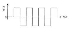
또한, 일실시형태의 발광 장치에서는 상기 교류 전원으로부터 받는 교류는 구형파이다.In the light emitting device of one embodiment, the alternating current received from the alternating current power source is a square wave.
이 실시형태에 의하면, 구형파의 교류로 발광 다이오드를 구동하므로 발광 다이오드를 가장 효율 좋게 발광시킬 수 있다. 예컨대, 정현파의 교류로 발광 다이오드를 구동할 경우, 정현파의 상승과 하강의 구배가 있으므로 평균 발광 강도가 약해진다.According to this embodiment, since the light emitting diode is driven by alternating square waves, the light emitting diode can be emitted most efficiently. For example, when the light emitting diode is driven by alternating sine waves, the average luminescence intensity is weakened because there is a gradient between rising and falling sine waves.
또한, 일실시형태의 발광 장치에서는 1개의 기판 상에 상기 제 1 전극과 제 2 전극이 형성되어 있다.In the light emitting device of one embodiment, the first electrode and the second electrode are formed on one substrate.
이 실시형태에 의하면, 1개의 기판 상에 제 1, 제 2 전극 및 복수개의 발광 다이오드를 실장할 수 있다.According to this embodiment, the 1st, 2nd electrode, and some light emitting diode can be mounted on one board | substrate.
또한, 일실시형태의 발광 장치에서는 상기 제 1 전극과 제 2 전극은 상기 기판 표면을 따라 연장되어 있음과 아울러 서로 대향하고 있고;In the light emitting device of one embodiment, the first electrode and the second electrode extend along the surface of the substrate and face each other;
상기 제 1 전극은 상기 제 2 전극을 향해서 돌출되어 있음과 아울러 상기 연장 방향을 따라 나열되도록 형성된 복수개의 돌출부를 갖고;The first electrode protrudes toward the second electrode and has a plurality of protrusions formed to line up in the extending direction;
상기 제 2 전극은 상기 제 1 전극을 향해서 돌출되어 있음과 아울러 상기 연장 방향을 따라 나열되도록 형성된 복수개의 돌출부를 갖고;The second electrode protrudes toward the first electrode and has a plurality of protrusions formed to line up along the extension direction;
상기 제 1 전극의 돌출부와 상기 제 2 전극의 돌출부가 대향하고 있고;The protrusion of the first electrode is opposite to the protrusion of the second electrode;
상기 제 1 발광 다이오드는,The first light emitting diode,
상기 제 1 전극의 돌출부에 애노드가 접속되어 있음과 아울러 상기 제 2 전극의 돌출부에 캐소드가 접속되고;An anode is connected to the protrusion of the first electrode and a cathode is connected to the protrusion of the second electrode;
상기 제 2 발광 다이오드는,The second light emitting diode,
상기 제 1 전극의 돌출부에 캐소드가 접속되어 있음과 아울러 상기 제 2 전극의 돌출부에 애노드가 접속되어 있다.A cathode is connected to the protruding portion of the first electrode and an anode is connected to the protruding portion of the second electrode.
이 실시형태에 의하면, 기판 상에서 상기 제 1, 제 2 전극이 연장되어 있는 방향을 따라 형성된 제 1, 제 2 전극의 돌출부 사이에 제 1, 제 2 발광 다이오드가 접속되어 있으므로 상기 전극의 연장 방향을 따라 상기 돌출부간의 간격으로 복수개의 발광 다이오드를 배치할 수 있다. 즉, 상기 기판 상에 형성한 제 1, 제 2 전극 및 그 돌출부에 의해 상기 복수개의 발광 다이오드의 배치를 설정할 수 있다.According to this embodiment, since the first and second light emitting diodes are connected between the protrusions of the first and second electrodes formed along the direction in which the first and second electrodes extend on the substrate, the extending direction of the electrodes is changed. Accordingly, a plurality of light emitting diodes may be arranged at intervals between the protrusions. That is, the arrangement of the plurality of light emitting diodes can be set by the first and second electrodes formed on the substrate and the protrusions thereof.
또한, 일실시형태의 발광 장치에서는 최대 치수가 100㎛ 이하이다.In the light emitting device of one embodiment, the maximum dimension is 100 μm or less.
이 실시형태에 의하면, 상기 발광 다이오드의 최대 치수가 100㎛ 이하이다. 이러한 미세 사이즈의 물체(발광 다이오드)를 방향도 고려해서 배치하기 위해서는 미세 사이즈의 물체를 미리 방향을 정렬시켜 준비해 두는 것이 필요하게 된다. 또는, 미세한 사이즈의 물체를 쥐고나서 방향을 정렬하는 작업이 필요하게 된다. 따라서, 이 실시형태와 같이, 발광 다이오드의 최대 치수가 100㎛ 이하의 미세한 경우에는 발광 다이오드의 방향이 랜덤이여도 좋으므로 본 발명에 적합하게 된다. 또한, 발광 다이오드의 사이즈가 작으므로 열이 발광 영역에 틀어박히지 않아 열에 의한 출력 저하나 수명 저하를 방지할 수 있다.According to this embodiment, the largest dimension of the said light emitting diode is 100 micrometers or less. In order to arrange such fine sized objects (light emitting diodes) in consideration of the direction, it is necessary to prepare the fine sized objects in alignment in advance. Or, it is necessary to align the direction after holding a fine-sized object. Therefore, as in this embodiment, when the maximum dimension of the light emitting diode is fine, 100 mu m or less, since the direction of the light emitting diode may be random, it is suitable for the present invention. In addition, since the size of the light emitting diode is small, heat does not get stuck in the light emitting region, and thus output reduction and life degradation due to heat can be prevented.
또한, 일실시형태의 발광 장치에서는 상기 발광 다이오드는 봉형상이다.In the light emitting device of one embodiment, the light emitting diode is rod-shaped.
이 실시형태에 의하면, 발광 다이오드가 봉형상이므로 배치 방향을 제어하기 쉽다.According to this embodiment, since the light emitting diode is rod-shaped, it is easy to control the arrangement direction.
또한, 일실시형태의 발광 장치에서는,In the light emitting device of one embodiment,
상기 제 1, 제 2 전극에 상기 발광 다이오드를 구성하는 반도체층이 직접 접속되어 있다.The semiconductor layer which comprises the said light emitting diode is directly connected to the said 1st, 2nd electrode.
이 실시형태에 의하면, 상기 발광 다이오드를 일방향으로 정렬하기 위한 방향성을 식별하기 위한 구조(예컨대 편방이 긴 리드선 등)가 존재하지 않으므로 상기 발광 다이오드의 제조 공정이 간략화된다.According to this embodiment, there is no structure for identifying the directionality for aligning the light emitting diodes in one direction (for example, a long one-sided lead wire, etc.), thereby simplifying the manufacturing process of the light emitting diodes.
또한, 일실시형태의 발광 장치에서는,In the light emitting device of one embodiment,
상기 발광 다이오드는,The light emitting diode,
제 1 도전형의 코어부와,The core portion of the first conductivity type,
상기 제 1 도전형의 코어부의 외주면을 피복하는 제 2 도전형의 쉘부를 갖고;A shell portion of the second conductivity type covering the outer circumferential surface of the core portion of the first conductivity type;
상기 제 1 도전형의 코어부의 외주면의 일부가 상기 제 2 도전형의 쉘부로부터 노출되어 있다.A part of the outer peripheral surface of the core portion of the first conductivity type is exposed from the shell portion of the second conductivity type.
이 실시형태에 의하면, 상기 제 1 도전형의 코어부와 제 2 도전형의 쉘부의 접합면을 코어부의 외주면을 따라 형성할 수 있어 발광면의 증대를 도모할 수 있다. 또한, 상기 코어부의 외주면의 일부가 제 2 도전형의 쉘부로부터 노출되어 있으므로 상기 코어부의 외주면의 일부로의 전극의 접속이 용이해진다.According to this embodiment, the joining surface of the core portion of the first conductive type and the shell portion of the second conductivity type can be formed along the outer circumferential surface of the core portion, and the light emitting surface can be increased. Moreover, since a part of the outer peripheral surface of the said core part is exposed from the shell part of a 2nd conductivity type, connection of an electrode to a part of the outer peripheral surface of the said core part becomes easy.
또한, 일실시형태의 발광 장치에서는In the light emitting device of one embodiment,
상기 발광 다이오드의 코어부는 원 기둥 형상이며;The core portion of the light emitting diode has a circular columnar shape;
상기 발광 다이오드의 쉘부는 상기 원 기둥 형상의 코어부의 외주면을 피복하고;The shell portion of the light emitting diode covers an outer circumferential surface of the circular columnar core portion;
상기 원 기둥 형상의 코어부의 외주면의 일부가 상기 쉘부로부터 노출되어 있고;A part of an outer circumferential surface of the circular columnar core portion is exposed from the shell portion;
상기 원 기둥 형상의 코어부와 상기 쉘부의 접합면은 상기 코어부의 둘레에 동심원상으로 형성되어 있다.The joining surface of the said columnar core part and the said shell part is formed concentrically around the said core part.
이 실시형태에 의하면, 상기 제 1 도전형의 원 기둥 형상의 코어부와 제 2 도전형의 쉘부의 접합면을 코어부의 외주면을 따라 원통 형상으로 형성할 수 있어 발광면의 증대를 도모할 수 있다. 또한, 상기 코어부의 외주면의 일부가 제 2 도전형의 쉘부로부터 노출되어 있으므로 상기 코어부의 외주면의 일부로의 전극의 접속이 용이해진다.According to this embodiment, the joining surface of the said 1st conductivity type circular columnar core part and the 2nd conductivity type shell part can be formed in cylindrical shape along the outer peripheral surface of a core part, and the light emitting surface can be increased. . Moreover, since a part of the outer peripheral surface of the said core part is exposed from the shell part of a 2nd conductivity type, connection of an electrode to a part of the outer peripheral surface of the said core part becomes easy.
또한, 일실시형태의 디스플레이용 백라이트는 상기 발광 장치를 가지므로 제조가 용이하며 제조 비용이 억제된다.In addition, since the backlight for a display of the embodiment has the above light emitting device, manufacturing is easy and manufacturing cost is suppressed.
또한, 일실시형태의 조명 장치는 상기 발광 장치를 가지므로 제조가 용이하며 제조 비용이 억제된다.Moreover, since the illuminating device of one embodiment has the above light emitting device, manufacturing is easy and manufacturing cost is suppressed.
또한, 일실시형태의 LED 디스플레이는 상기 발광 장치를 가지므로 제조가 용이하며 제조 비용이 억제된다.In addition, since the LED display of one embodiment has the above light emitting device, manufacturing is easy and manufacturing cost is suppressed.
또한, 일실시형태의 발광 장치의 제조 방법에서는,Moreover, in the manufacturing method of the light emitting device of one embodiment,
제 1 전극과 제 2 전극을 갖는 기판을 준비하는 공정;Preparing a substrate having a first electrode and a second electrode;
상기 기판에 최대 치수가 100㎛ 이하인 복수개의 발광 다이오드를 포함한 용액을 도포하는 공정; 및Applying a solution including a plurality of light emitting diodes having a maximum dimension of 100 μm or less on the substrate; And
상기 제 1 전극과 제 2 전극에 전압을 인가해서 상기 발광 다이오드를 상기 제 1, 제 2 전극에 의해 규정되는 위치에 배열시키는 공정을 구비한다.And applying a voltage to the first electrode and the second electrode to arrange the light emitting diode at a position defined by the first and second electrodes.
이 실시형태의 제조 방법에 의하면, 소위 유전 영동을 이용해서 상기 제 1, 제 2 전극에 의해 규정되는 위치에 미세한 발광 다이오드를 배치할 수 있다. 이 제조 방법에서는 발광 다이오드의 방향을 한쪽으로 정하는 것이 곤란하므로 발광 다이오드의 방향(극성)이 혼재되어 있는 본 발명의 발광 장치를 제조하는데에 바람직하다.According to the manufacturing method of this embodiment, fine light emitting diodes can be arranged at positions defined by the first and second electrodes by using so-called dielectric electrophoresis. In this manufacturing method, since it is difficult to determine the direction of a light emitting diode to one side, it is preferable to manufacture the light emitting device of this invention in which the direction (polarity) of a light emitting diode is mixed.
또한, 본 발명의 다른 실시형태에 의하면, 본 발명의 발광 장치는,Moreover, according to another embodiment of the present invention, the light emitting device of the present invention,
기판 상에 형성된 제 1 전극;A first electrode formed on the substrate;
상기 기판 상에 형성된 제 2 전극;A second electrode formed on the substrate;
상기 기판 상에 형성된 제 3 전극; 및A third electrode formed on the substrate; And
제 1 도전형의 제 1 영역과 제 2 도전형의 제 2 영역과 제 1 도전형의 제 3 영역을 가짐과 아울러 상기 제 1, 제 2, 제 3 영역이 상기 제 1, 제 2, 제 3 영역의 순서로 나열된 봉형상 발광 소자를 구비하고:It has a 1st area | region of a 1st conductivity type, a 2nd area | region of a 2nd conductivity type, and a 3rd area | region of a 1st conductivity type, and the said 1st, 2nd, 3rd area | region is said 1st, 2nd, 3rd And having rod-shaped light emitting elements arranged in order of regions:
상기 제 1 영역이 상기 제 1 전극 또는 제 3 전극 중 한쪽에 접속되고, 상기 제 2 영역이 상기 제 2 전극에 접속되며, 상기 제 3 영역이 상기 제 1 전극 또는 제 3 전극 중 다른쪽에 접속되어 있는 것을 특징으로 하고 있다.The first region is connected to one of the first electrode or the third electrode, the second region is connected to the second electrode, and the third region is connected to the other of the first electrode or third electrode, It is characterized by that.
본 발명의 발광 장치에 의하면, 상기 봉형상 발광 소자의 제 2 도전형의 제 2 영역의 양측에 제 1 도전형의 제 1 영역과 제 1 도전형의 제 3 영역이 배치되어 있다. 따라서, 상기 제 1, 제 3 전극에 대한 봉형상 발광 소자의 제 1, 제 3 영역의 접속이 교체되어도 제 1, 제 3 전극에 대한 다이오드 극성이 교체되지 않으므로 정상으로 발광 가능하게 된다. 따라서, 제조 공정에서 제 1, 제 3 전극에 대한 제 1, 제 3 영역의 접속이 반대로 되어도 좋고, 봉형상 발광 소자의 방향성을 식별하기 위한 마크나 형상도 불필요하게 되어 제조 공정을 간략화할 수 있고 제조 비용을 억제할 수 있다.According to the light emitting device of the present invention, the first region of the first conductivity type and the third region of the first conductivity type are arranged on both sides of the second region of the second conductivity type of the rod-shaped light emitting element. Therefore, even if the connection of the first and third regions of the rod-shaped light emitting element to the first and third electrodes is replaced, the diode polarity to the first and third electrodes is not replaced, so that light emission can be performed normally. Therefore, in the manufacturing process, the connection of the first and third regions to the first and third electrodes may be reversed, and a mark or shape for identifying the directionality of the rod-shaped light emitting element is also unnecessary, and the manufacturing process can be simplified. Manufacturing cost can be held down.
일실시형태에서는,In one embodiment,
상기 제 1 전극 또는 제 3 전극 중 한쪽으로부터 상기 제 1 영역과 제 2 영역을 순서대로 경유해서 상기 제 2 전극으로 전류가 흐르는 제 1 통전 방향과, 상기 제 2 전극으로부터 상기 제 2 영역과 제 1 영역을 순서대로 경유해서 상기 제 1 전극 또는 제 3 전극 중 한쪽으로 전류가 흐르는 제 2 통전 방향 중 어느 한쪽의 통전 방향으로 통전되거나, 또는, 상기 제 1 전극 또는 제 3 전극 중 다른쪽으로부터 상기 제 3 영역과 제 2 영역을 순서대로 경유해서 상기 제 2 전극으로 전류가 흐르는 제 3 통전 방향과, 상기 제 2 전극으로부터 상기 제 2 영역과 제 3 영역을 순서대로 경유해서 상기 제 1 전극 또는 제 3 전극 중 다른쪽으로 전류가 흐르는 제 4 통전 방향 중 어느 한쪽의 통전 방향으로 통전된다.A first conduction direction in which current flows from the first electrode or the third electrode to the second electrode via the first region and the second region in order; and the second region and the first electrode from the second electrode. Energized in one of the second energization directions in which current flows to one of the first and third electrodes via the region in order, or from the other of the first or third electrodes A third conduction direction in which current flows to the second electrode via the third region and the second region in order, and the first electrode or the third through the second region and the third region from the second electrode in order; The current is supplied in one of the fourth energization directions in which current flows to the other of the electrodes.
또한, 일실시형태에서는,In addition, in one embodiment,
상기 제 1 전극 또는 제 3 전극 중 한쪽으로부터 상기 제 1 영역과 제 2 영역을 순서대로 경유해서 상기 제 2 전극으로 전류가 흐름과 아울러 상기 제 1 전극 또는 제 3 전극 중 다른쪽으로부터 상기 제 3 영역과 제 2 영역을 순서대로 경유해서 상기 제 2 전극으로 전류가 흐르는 제 1 통전 방향과, 상기 제 2 전극으로부터 상기 제 2 영역과 제 1 영역을 순서대로 경유해서 상기 제 1 전극 또는 제 3 전극 중 한쪽으로 전류가 흐름과 아울러 상기 제 2 전극으로부터 상기 제 2 영역과 제 3 영역을 순서대로 경유해서 상기 제 1 전극 또는 제 3 전극 중 다른쪽으로 전류가 흐르는 제 2 통전 방향 중 어느 한쪽의 통전 방향으로 통전된다.The current flows to the second electrode via the first region and the second region in order from one of the first electrode or the third electrode, and the third region from the other of the first electrode or the third electrode. And a first conduction direction in which current flows to the second electrode via the second region in order, and the first electrode or the third electrode via the second region and the first region in order from the second electrode. The current flows to one side, and in one of the second energization directions in which current flows to the other of the first electrode and the third electrode via the second region and the third region in order from the second electrode. It is energized.
또한, 일실시형태의 발광 장치에서는 상기 제 1 영역의 일단부와 상기 제 2 영역의 타단부가 접합되어 있음과 아울러 상기 제 2 영역의 일단부와 상기 제 3 영역의 타단부가 접합되어 있고,In the light emitting device of one embodiment, one end of the first region and the other end of the second region are joined, and one end of the second region and the other end of the third region are joined.
상기 제 1 영역의 타단부가 상기 제 1 전극 또는 제 3 전극 중 한쪽에 접속되어 있음과 아울러 상기 제 3 영역의 일단부가 상기 제 1 전극 또는 제 3 전극 중 다른쪽에 접속되어 있다.The other end of the first region is connected to one of the first electrode or the third electrode, and one end of the third region is connected to the other of the first electrode or the third electrode.
이 실시형태의 발광 장치에 의하면, 상기 봉형상 발광 소자를 제 1, 제 2, 제 3 영역이 순서대로 접합된 봉형상으로 해서 봉형상 발광 소자의 구조를 간략화할 수 있다.According to the light emitting device of this embodiment, the structure of the rod-shaped light emitting element can be simplified by making the rod-shaped light emitting element into a rod shape in which the first, second and third regions are joined in order.
또한, 일실시형태의 발광 장치에서는 상기 봉형상 발광 소자는,In the light emitting device of one embodiment, the rod-shaped light emitting element is
상기 제 1 영역과 상기 제 3 영역이 봉형상으로 연이어져 구성되어 있음과 아울러 상기 제 2 영역을 관통하고 있는 코어부와,A core portion having the first region and the third region connected in a rod shape and penetrating the second region;
상기 제 2 영역으로 구성되어 있음과 아울러 상기 코어부의 외주면을 피복하는 쉘부를 구비하고;A shell portion formed of the second region and covering an outer circumferential surface of the core portion;
상기 쉘부의 양단으로부터 상기 코어부의 상기 제 1 영역과 제 3 영역이 노출되어 있다.The first region and the third region of the core portion are exposed from both ends of the shell portion.
이 실시형태의 발광 장치에 의하면, 상기 봉형상 발광 소자는 제 1 도전형의 제 1, 제 3 영역에 의한 코어부의 외주면과 제 2 도전형의 제 2 영역에 의한 쉘부의 내주면의 접합면(PN 접합면)이 발광면이 되므로 발광 면적을 크게 취할 수 있어 큰 발광 강도를 얻을 수 있다.According to the light emitting device of this embodiment, the rod-shaped light emitting element is a joining surface (PN) between the outer circumferential surface of the core portion by the first and third regions of the first conductivity type and the inner circumferential surface of the shell portion by the second region of the second conductivity type. Since the bonding surface) becomes a light emitting surface, the light emitting area can be large and a large light emitting intensity can be obtained.
또한, 일실시형태의 발광 장치에서는 상기 봉형상 발광 소자의 최대 치수가 100㎛ 이하이다.In the light emitting device of one embodiment, the maximum dimension of the rod-shaped light emitting element is 100 µm or less.
이 실시형태의 발광 장치에 의하면, 상기 봉형상 발광 소자의 최대 치수가 100㎛ 이하이다. 이러한 미세 사이즈의 물체인 봉형상 발광 소자를 방향도 고려해서 배치하기 위해서는 이 미세 사이즈의 봉형상 발광 소자를 미리 방향을 정렬시켜 준비해 두는 것이 필요하게 된다. 또는, 상기 미세한 사이즈의 봉형상 발광 소자를 쥐고나서 방향을 정렬하는 작업이 필요하게 된다. 따라서, 이 실시형태와 같이, 봉형상 발광 소자의 최대 치수가 100㎛ 이하의 미세한 경우에는 봉형상 발광 소자의 방향을 정렬할 필요가 없는 본 발명에 적합하게 된다. 또한, 봉형상 발광 소자의 사이즈가 100㎛ 이하의 작은 사이즈이므로 열이 발광 영역에 틀어박히지 않아 열에 의한 출력 저하나 수명 저하를 방지할 수 있다.According to the light emitting device of this embodiment, the maximum dimension of the rod-shaped light emitting element is 100 µm or less. In order to arrange the rod-shaped light emitting element which is such a micro-sized object in consideration of the direction, it is necessary to arrange the rod-shaped light emitting element of the micro size in advance and arrange the direction. Alternatively, after grasping the rod-shaped light-emitting device of the fine size, it is necessary to align the direction. Therefore, as in this embodiment, when the maximum dimension of the rod-shaped light emitting element is minute or less, it is suitable for the present invention which does not need to align the direction of the rod-shaped light emitting element. In addition, since the rod-shaped light emitting element has a small size of 100 µm or less, heat does not get stuck in the light emitting region, and thus output reduction and life degradation due to heat can be prevented.
또한, 일실시형태의 디스플레이용 백라이트에서는 상기 발광 장치를 가지므로 제조가 용이하며 제조 비용이 억제된다.In addition, the display backlight of the embodiment has the above light emitting device, so that the manufacturing is easy and the manufacturing cost is suppressed.
또한, 일실시형태의 조명 장치는 상기 발광 장치를 가지므로 제조가 용이하며 제조 비용이 억제된다.Moreover, since the illuminating device of one embodiment has the above light emitting device, manufacturing is easy and manufacturing cost is suppressed.
또한, 일실시형태의 LED 디스플레이는 상기 발광 장치를 가지므로 제조가 용이하며 제조 비용이 억제된다.In addition, since the LED display of one embodiment has the above light emitting device, manufacturing is easy and manufacturing cost is suppressed.
또한, 일실시형태의 발광 장치의 제조 방법에서는 제 1 전극과 제 2 전극 및 제 3 전극을 갖는 기판을 준비하는 공정;Moreover, the manufacturing method of the light emitting device of one Embodiment is a process of preparing the board | substrate which has a 1st electrode, a 2nd electrode, and a 3rd electrode;
상기 기판에, 제 1 도전형의 제 1 영역과 제 2 도전형의 제 2 영역과 제 1 도전형의 제 3 영역을 가짐과 아울러 상기 제 1, 제 2, 제 3 영역이 상기 제 1, 제 2, 제 3 영역의 순서로 나열되어 있고 최대 치수가 100㎛ 이하인 복수개의 봉형상 발광 소자를 포함한 용액을 도포하는 공정; 및The substrate has a first region of a first conductivity type, a second region of a second conductivity type, and a third region of a first conductivity type, and the first, second, and third regions comprise the first, second, and third regions. 2, a process of applying a solution including a plurality of rod-shaped light emitting elements having a maximum dimension of 100 µm or less, arranged in order of the third region; And
상기 제 1 전극과 제 3 전극에 전압을 인가해서 상기 복수개의 봉형상 발광 소자를 상기 제 1, 제 2, 제 3 전극에 의해 규정되는 위치에 배열시키는 공정을 구비한다.And arranging the plurality of rod-shaped light emitting elements at positions defined by the first, second, and third electrodes by applying a voltage to the first electrode and the third electrode.
이 실시형태의 발광 장치의 제조 방법에 의하면, 소위 유전 영동을 이용해서 상기 제 1, 제 2, 제 3 전극에 의해 규정되는 위치에 최대 치수가 100㎛ 이하의 미세한 상기 봉형상 발광 소자를 배치할 수 있다. 이 제조 방법에서는 상기 봉형상 발광 소자의 방향을 한쪽으로 정하는 것이 곤란하므로 상기 봉형상 발광 소자의 방향을 한쪽으로 규정할 필요가 없는 본 발명의 발광 장치의 제조 방법으로서 바람직하다.According to the manufacturing method of the light emitting device of this embodiment, the fine rod-shaped light emitting element having a maximum dimension of 100 µm or less can be disposed at a position defined by the first, second, and third electrodes by using so-called dielectric electrophoresis. Can be. In this manufacturing method, since it is difficult to determine the direction of the rod-shaped light emitting element to one side, it is preferable as the manufacturing method of the light emitting device of the present invention which does not need to define the direction of the rod-shaped light emitting element to one side.
<발명의 효과>Effect of the Invention
본 발명의 발광 장치에 의하면, 병렬로 접속되는 복수개의 발광 다이오드의 극성을 정렬시켜 배열할 필요가 없으므로 제조시에 복수개의 발광 다이오드의 극성(방향)을 정렬하는 공정이 불필요하게 되어 공정을 간략화할 수 있다. 또한, 발광 다이오드의 극성(방향)을 식별하기 위해서 발광 다이오드에 마크를 설치할 필요가 없고, 발광 다이오드를 특별한 형상으로 할 필요가 없어진다. 따라서, 발광 다이오드의 제조 공정을 간략화할 수 있고, 제조 비용도 억제할 수 있다.According to the light emitting device of the present invention, it is not necessary to arrange and arrange the polarities of the plurality of light emitting diodes connected in parallel, so that the process of aligning the polarities (directions) of the plurality of light emitting diodes is unnecessary at the time of manufacture, thereby simplifying the process. Can be. In addition, in order to identify the polarity (direction) of the light emitting diode, there is no need to provide a mark on the light emitting diode, and the light emitting diode does not need to have a special shape. Therefore, the manufacturing process of a light emitting diode can be simplified and manufacturing cost can also be suppressed.
또한, 본 발명의 발광 장치에 의하면, 봉형상 발광 소자의 제 2 도전형의 제 2 영역의 양측에 제 1 도전형의 제 1 영역과 제 1 도전형의 제 3 영역이 배치되어 있다. 따라서, 제 1, 제 3 전극에 대한 봉형상 발광 소자의 제 1, 제 3 영역의 방향이 교체되어도 극성이 교체되지 않으므로 정상으로 발광 가능하게 된다. 따라서, 제조 공정에서 제 1, 제 3 전극에 대한 제 1, 제 3 영역의 접속이 반대로 되어도 좋고, 제조 공정을 간략화할 수 있어 제조 비용을 억제할 수 있다.According to the light emitting device of the present invention, the first region of the first conductivity type and the third region of the first conductivity type are arranged on both sides of the second region of the second conductivity type of the rod-shaped light emitting element. Therefore, even if the directions of the first and third regions of the rod-shaped light emitting elements with respect to the first and third electrodes are reversed, the polarity is not changed. Therefore, the connection of the 1st, 3rd area | region to 1st, 3rd electrode may be reversed in a manufacturing process, manufacturing process can be simplified, and manufacturing cost can be suppressed.
본 발명은 이하의 상세한 설명과 첨부된 도면으로부터 보다 충분하게 이해할 수 있을 것이다. 첨부된 도면은 설명을 위한 것뿐으로서 본 발명을 제한하는 것은 아니다.The invention will be more fully understood from the following detailed description and the accompanying drawings. The accompanying drawings are for illustrative purposes only and do not limit the invention.
도 1은 본 발명의 발광 장치의 제 1 실시형태의 전기 회로 구성을 모식적으로 나타내는 도면이다.
도 2는 상기 실시형태를 구동하는 교류 전원의 교류 파형의 일례를 나타내는 파형도이다.
도 3은 본 발명의 발광 장치의 제 2 실시형태의 전기 회로 구성을 나타내는 회로도이다.
도 4는 상기 실시형태의 변형예를 나타내는 회로도이다.
도 5는 상기 실시형태의 또 하나의 변형예를 나타내는 회로도이다.
도 6은 상기 실시형태의 각 병렬 구성 단위에 있어서 발광 다이오드를 병렬로 접속하는 개수(m)와 상기 병렬 구성 단위를 직렬로 접속하는 개수(n)에 대한 불량률(P)을 나타내는 도면이다.
도 7은 본 발명의 발광 장치의 제 3 실시형태를 나타내는 모식적인 평면도이다.
도 8A는 상기 실시형태의 발광 다이오드의 구성의 일례를 나타내는 사시도이다.
도 8B는 상기 발광 다이오드의 단면도이다.
도 9A는 봉형상 구조의 발광 다이오드의 제조 방법의 공정도이다.
도 9B는 도 9A에 계속되는 봉형상 구조 발광 소자의 제조 방법의 공정도이다.
도 9C는 도 9B에 계속되는 봉형상 구조 발광 소자의 제조 방법의 공정도이다.
도 9D는 도 9C에 계속되는 봉형상 구조 발광 소자의 제조 방법의 공정도이다.
도 9E는 도 9D에 계속되는 봉형상 구조 발광 소자의 제조 방법의 공정도이다.
도 10은 본 발명의 제 5 실시형태로서의 LED 디스플레이의 1화소의 회로를 나타내는 도면이다.
도 11은 본 발명의 발광 장치의 제 6 실시형태를 나타내는 평면도이다.
도 12는 본 발명의 발광 장치의 제 7 실시형태를 나타내는 평면도이다.
도 13A는 상기 제 7 실시형태가 구비하는 봉형상 발광 소자의 측면도이다.
도 13B는 상기 봉형상 발광 소자의 단면도이다.
도 14는 본 발명의 발광 장치의 제 8 실시형태를 나타내는 평면도이다.
도 15A는 도 9C에 계속되는 봉형상 구조 발광 소자의 제조 방법의 공정도이다.
도 15B는 도 15A에 계속되는 봉형상 구조 발광 소자의 제조 방법의 공정도이다.
도 16은 본 발명의 제 10 실시형태로서의 LED 디스플레이의 1화소의 회로를 나타내는 도면이다.
도 17은 제 1 종래의 발광 장치를 나타내는 도면이다.
도 18은 제 2 종래의 발광 장치를 나타내는 사시도이다.BRIEF DESCRIPTION OF THE DRAWINGS It is a figure which shows typically the electric circuit structure of 1st Embodiment of the light-emitting device of this invention.
2 is a waveform diagram illustrating an example of an AC waveform of an AC power supply for driving the above embodiment.
3 is a circuit diagram showing the electrical circuit configuration of the second embodiment of the light emitting device of the present invention.
4 is a circuit diagram showing a modification of the above embodiment.
5 is a circuit diagram showing yet another modification of the embodiment.
FIG. 6: is a figure which shows the defective rate P with respect to the number m which connects a light emitting diode in parallel, and the number n which connects the said parallel structural units in series in each parallel structural unit of the said embodiment.
7 is a schematic plan view showing a third embodiment of the light emitting device of the present invention.
8A is a perspective view illustrating an example of the configuration of the light emitting diode of the above embodiment.
8B is a cross-sectional view of the light emitting diode.
9A is a flowchart of a method of manufacturing a light emitting diode having a rod-like structure.
FIG. 9B is a flowchart of a method of manufacturing a rod-shaped structure light emitting device subsequent to FIG. 9A. FIG.
9C is a flowchart of a method of manufacturing a rod-shaped structure light emitting device subsequent to FIG. 9B.
9D is a flowchart of a method of manufacturing a rod-shaped structure light emitting device subsequent to FIG. 9C.
9E is a flowchart of a method of manufacturing a rod-shaped structure light emitting device subsequent to FIG. 9D.
It is a figure which shows the circuit of one pixel of the LED display as 5th Embodiment of this invention.
11 is a plan view showing a sixth embodiment of a light emitting device of the present invention.
12 is a plan view showing a seventh embodiment of a light emitting device of the present invention.
FIG. 13A is a side view of a rod-shaped light emitting element included in the seventh embodiment. FIG.
Fig. 13B is a sectional view of the rod-shaped light emitting device.
14 is a plan view showing an eighth embodiment of a light emitting device of the present invention.
FIG. 15A is a flowchart of a method of manufacturing a rod-shaped structure light emitting device subsequent to FIG. 9C. FIG.
FIG. 15B is a flowchart of the method of manufacturing the rod-shaped structure light emitting device subsequent to FIG. 15A. FIG.
It is a figure which shows the circuit of one pixel of the LED display as a 10th embodiment of the present invention.
17 is a view showing a first conventional light emitting device.
18 is a perspective view showing a second conventional light emitting device.
이하, 본 발명을 도시의 실시형태에 의해 상세하게 설명한다.EMBODIMENT OF THE INVENTION Hereinafter, this invention is demonstrated in detail by embodiment of illustration.
(제 1 실시형태)(1st embodiment)
도 1에 본 발명의 발광 장치의 제 1 실시형태의 전기 회로 구성을 모식적으로 나타낸다. 이 제 1 실시형태의 발광 장치는 제 1 전극(1) 및 제 2 전극(2)과, 상기 제 1 전극(1)과 제 2 전극(2) 사이에 병렬로 접속된 5개의 발광 다이오드(3~7)를 구비한다. 상기 발광 다이오드(3,4,6)는 제 2 발광 다이오드이며, 제 1 전극(1)에 캐소드가 접속되어 있음과 아울러 상기 제 2 전극(2)에 애노드가 접속되어 있다. 한편, 상기 발광 다이오드(5,7)는 제 1 발광 다이오드이며, 상기 제 1 전극(1)에 애노드가 접속되어 있음과 아울러 제 2 전극(2)에 캐소드가 접속되어 있다. 상기 제 1 전극(1)과 제 2 전극(2)에는 교류 전원(10)이 접속되고, 이 교류 전원(10)은 상기 제 1 전극(1)과 제 2 전극(2)에 교류 전압을 인가한다. 이 실시형태에서는 상기 교류 전원(10)에 의한 교류 전압의 주파수를 60㎐로 했다. 도 1에 나타내는 바와 같이, 상기 5개의 발광 다이오드(3~7)는 제 1 전극(1)에 캐소드가 접속되어 있는 발광 다이오드(3,4,6)와 제 2 전극(2)에 캐소드가 접속되어 있는 발광 다이오드(5,7)가 상기 제 1 전극(1)과 제 2 전극(2) 사이에서 혼재해서 배치되어 있다. 본 실시형태에서는 5개의 발광 다이오드(3~7) 중 3개가 일방향으로 접속[제 1 전극(1)에 캐소드가 접속]되고, 나머지 2개가 다른 방향으로 접속[제 2 전극(2)에 캐소드가 접속]되어 있다. 그러나, 이 일방향으로 접속된 발광 다이오드의 개수와 다른 방향으로 접속된 발광 다이오드의 개수의 비율은 이것에 한정되는 것은 아니며 다른 비율이여도 좋다. 즉, 일방향으로 접속되는 발광 다이오드와 다른 방향으로 접속되는 발광 다이오드의 수는 동수(同數) 정도가 아니어도 좋고, 그 비율이 일정하지 않아도 좋다. 이것은, 본 발명의 발광 장치의 제조시에 발광 다이오드의 방향을 제어할 필요가 없고, 랜덤하게 배열해도 좋은 것을 나타내고 있다. 또한, 일방향으로 접속되는 발광 다이오드와 다른 방향으로 접속되는 발광 다이오드의 수의 비가 현저하게 커졌을 경우에는 발광의 흔들림의 원인이 되는 경우가 있지만 이것을 억제하기 위한 방법은 후술한다.In FIG. 1, the electric circuit structure of 1st Embodiment of the light-emitting device of this invention is shown typically. The light emitting device of the first embodiment includes five
이 실시형태의 발광 장치에 의하면, 상기 제 1 전극(1)과 제 2 전극(2) 사이에 병렬로 접속되는 5개의 발광 다이오드(3~7)의 극성을 정렬시켜 배열할 필요가 없으므로 제조시에 5개의 발광 다이오드(3~7)의 극성(방향)을 정렬하는 공정이 불필요하게 되어 공정을 간략화할 수 있다. 또한, 상기 발광 다이오드(3~7)의 극성(방향)을 식별하기 위해서 발광 다이오드(3~7)에 마크를 설치할 필요가 없고, 극성 식별을 위해서 발광 다이오드(3~7)를 특별한 형상으로 할 필요도 없어진다.According to the light emitting device of this embodiment, since the polarities of the five
따라서, 이 실시형태의 발광 장치에 의하면, 발광 다이오드(3~7)의 제조 공정을 간략화할 수 있고, 제조 비용도 억제할 수 있다. 특히, 발광 다이오드(3~7)의 최대 치수가 100㎛ 이하의 작은 사이즈인 경우에는 미세 사이즈의 부품이 되어 극성(방향)을 정렬하는 작업이 어려워지므로 극성을 정렬시켜 발광 다이오드를 배열하는 경우에 비해서 제조 공정을 현격하게 간략화할 수 있다.Therefore, according to the light emitting device of this embodiment, the manufacturing process of the light emitting diodes 3-7 can be simplified, and manufacturing cost can also be suppressed. In particular, when the maximum size of the
또한, 상기 실시형태에서는 제 1 전극(1)과 제 2 전극(2) 사이에 접속되는 발광 다이오드의 개수를 5개로 했지만 5개 미만 또는 6개 이상으로 해도 좋다. 예컨대, 제 1 전극(1)과 제 2 전극(2) 사이에 접속되는 발광 다이오드의 개수를 100개 이상으로 함으로써 교류 구동에 의해 일어나는 점멸에 의한 흔들림을 억제할 수 있고, 밝기의 편차를 기대값의 10% 이하로 억제할 수 있게 된다. 이것에 대해서 이하에 설명한다.In addition, although the number of the light emitting diodes connected between the
즉, 상기 복수개의 발광 다이오드의 방향은 랜덤이며, 각 발광 다이오드에 대해서 한쪽의 방향과 다른쪽의 방향이 각각 2분의 1의 확률로 발생되기 때문에 p=0.5의 이항분포를 고려한다. 여기서, n개의 발광 다이오드가 있고, 소정 방향의 발광 다이오드를 X개(한번에 발광하는 다이오드의 개수)로 한다. 그러면, 이항분포의 성질로부터 X의 기대값[E(X)]은 E(X)=np이며, 분산[V(X)]=np(1-p)가 된다. 그리고, X가 그 기대값인 E(X)=np로부터 어느 정도 어긋나는지의 목표는 분산의 평방근{V(X)}1/2이며, 정규분포의 경우에는 표준편차라고 불린다. 이 목표(분산의 평방근)가 기대값의 10%가 될 경우, 다음 식(1)이 성립된다.That is, since the directions of the plurality of light emitting diodes are random, and one direction and the other direction are generated with a probability of 1/2 for each light emitting diode, a binomial distribution of p = 0.5 is considered. Here, there are n light emitting diodes, and the number of light emitting diodes in a predetermined direction is X (the number of diodes emitting light at one time). Then, from the property of the binomial distribution, the expected value of X [E (X)] is E (X) = np, and the variance [V (X)] = np (1-p). The target of how far X is from E (X) = np, the expected value, is the square root of the variance {V (X)}1/2 , and is called standard deviation in the case of normal distribution. When this target (square root of variance) is 10% of the expected value, the following equation (1) is established.
{np(1-p)}1/2=0.1np … (1){np (1-p)}1/2 = 0.1 np... (One)
이 식(1)에 p=0.5를 대입해서 n을 풀면 n=100이 된다. 이것은 밝기의 편차가 기대값의 10%가 되는 조건을 풀면 발광 다이오드의 개수가 100개인 것을 나타내고 있다.Solving n by substituting p = 0.5 in this equation (1) yields n = 100. This indicates that the number of light emitting diodes is 100 when the condition that the variation in brightness is 10% of the expected value is solved.
또한, 현재의 실질적인 제조 한계로부터 제 1 전극(1)과 제 2 전극(2) 사이에 접속할 수 있는 발광 다이오드의 개수의 상한값은 약 1억개이다. 이와 같이, 제 1 전극(1)과 제 2 전극(2) 사이에 접속되는 발광 다이오드의 개수가 많을 경우, 극성을 정렬시켜 발광 다이오드를 배열하는 것에 비해서 제조 공정을 현격하게 간략화할 수 있다.In addition, the upper limit of the number of light emitting diodes that can be connected between the
또한, 상기 실시형태에서는 상기 교류 전원(10)에 의한 교류 전압의 주파수를 60㎐로 했지만 상기 교류 전압의 주파수는 60㎐ 미만이여도 좋다. 무엇보다, 상기 교류 전압의 주파수를 60㎐ 이상으로 함으로써 교류 구동에 의해 일어나는 발광 다이오드의 점멸에 의한 흔들림을 억제할 수 있다. 한편, 상기 교류 전압의 주파수를 1㎒ 이하로 함으로써 고주파에 의한 배선 내에서의 손실을 억제할 수 있다. 교류 전원의 교류 주파수가 1㎒를 초과하면 고주파에 의한 배선 내에서의 손실을 무시할 수 없게 된다. 또한, 상기 교류 전압의 파형은 정현파, 삼각파, 구형파, 또는 그 외의 주기적으로 변화되는 교류 파형이여도 좋지만 구형파로 하는 것이 바람직하다. 일례로서, 도 2에 나타내는 바와 같은 구형파의 교류로 발광 다이오드를 구동함으로써 발광 다이오드를 가장 효율 좋게 발광시킬 수 있다. 이것에 대해서, 정현파의 교류로 발광 다이오드를 구동할 경우, 정현파의 상승과 하강의 구배가 있으므로 평균 발광 강도가 약해진다.In addition, in the said embodiment, although the frequency of the AC voltage by the said
또한, 도 1에서는 상기 제 1 전극(1)과 제 2 전극(2) 사이에 접속된 발광 다이오드(3~7)는 교류 전원(10)에 직접 접속되어 있지만 발광 다이오드(3~7)와 교류 전원(10) 사이에 다른 소자 또는 회로가 존재하고 있어도 좋다. 예컨대, 발광 다이오드(3~7)에 교류 전압이 인가되는 한에 있어서 발광 다이오드(3~7)와 교류 전원(10) 사이에 저항, 콘덴서, 다이오드, 트랜지스터, 그 외의 소자, 또는 이들을 조합시킨 회로가 있어도 좋다. 또한, 발광 다이오드(3~7)에 교류 전압이 인가되는 한에 있어서 발광 다이오드(3~7)와 병렬로 저항, 콘덴서, 다이오드, 트랜지스터, 그 외의 소자, 또는 이들을 조합시킨 회로가 있어도 좋다.In addition, in FIG. 1, the
또한, 이 실시형태에서는, 도 1에 나타내는 바와 같이, 발광 다이오드(3,4,6)가 일방향[캐소드가 제 1 전극(1)]으로 접속되고, 발광 다이오드(5,7)가 다른 방향[캐소드가 제 2 전극(2)]으로 접속되어 있다. 따라서, 상기 일방향으로 접속된 발광 다이오드(3,4,6)로부터 보면 상기 다른 방향으로 접속된 발광 다이오드(5,7)는 보호 다이오드의 역할을 하고 있다. 즉, 상기 일방향으로 접속된 발광 다이오드(3,4,6)에 서지 등에 의해 큰 역방향 전압이 인가된 경우에도 상기 다른 방향으로 접속된 발광 다이오드(5,7)에 즉시 순방향 전류가 흐르고, 도시하지 않은 전원(10) 중의 저항 또는 발광 다이오드와 전원(10) 사이에 설치된 저항에 의해 전압 강하가 일어나고, 상기 일방향으로 접속된 발광 다이오드(3,4,6)에 큰 역방향 전압이 인가되는 것을 방지할 수 있다. 마찬가지로, 상기 다른 방향으로 접속된 발광 다이오드(5,7)로부터 보면 상기 일방향으로 접속된 발광 다이오드(3,4,6)는 보호 다이오드의 역할을 하고 있다. 즉, 발광 다이오드(3~7)는 발광 다이오드로서의 기능뿐만 아니라 보호 다이오드로서의 기능을 발휘하게 된다. 이에 따라, 적은 부품으로 높은 신뢰성의 발광 장치를 얻을 수 있다.In this embodiment, as shown in FIG. 1, the
(제 2 실시형태)(2nd embodiment)
이어서, 도 3을 참조해서 본 발명의 발광 장치의 제 2 실시형태를 설명한다. 도 3은 이 제 2 실시형태의 전기 회로 구성을 모식적으로 나타내는 회로도이다.Next, with reference to FIG. 3, 2nd Embodiment of the light-emitting device of this invention is described. 3 is a circuit diagram schematically showing the electrical circuit configuration of the second embodiment.
도 3에 본 발명의 발광 장치의 제 2 실시형태의 전기 회로 구성을 모식적으로 나타낸다. 이 제 2 실시형태의 발광 장치는 제 1 전극(201) 및 제 2 전극(202)과, 상기 제 1 전극(201)과 제 2 전극(202) 사이에 직병렬로 접속된 24개의 발광 다이오드(311~316,321~326,331~336,341~346)로 이루어지는 발광 다이오드 회로(203)를 구비한다.3, the electric circuit structure of 2nd Embodiment of the light-emitting device of this invention is shown typically. The light emitting device of the second embodiment includes 24 light emitting diodes connected in series and in parallel between the
6개의 발광 다이오드(311~316)는 병렬로 접속되어 있고, 병렬 구성 단위(401)를 이루고 있다. 마찬가지로, 6개의 발광 다이오드(321~326), 6개의 발광 다이오드(331~336) 및 6개의 발광 다이오드(341~346)도 각각 병렬 구성 단위(402,403,404)를 이루고 있다. 이들 4개의 병렬 구성 단위(401~404)가 직렬로 접속되어 발광 다이오드 회로(203)를 이루고, 그 양단이 제 1 전극(201) 및 제 2 전극(202)에 접속되어 있다.The six
각 병렬 구성 단위(401~404)에서는 서로 역방향인 2개의 방향으로 접속된 발광 다이오드가 혼재하고 있다.In each parallel structural unit 401-404, light emitting diodes connected in two directions opposite to each other are mixed.
구체적으로는, 발광 다이오드(311~316)가 구성하는 병렬 구성 단위(401)에서는 제 2 발광 다이오드로서의 발광 다이오드(311,313,315,316)의 캐소드가 제 1 전극(201)에 직접 접속되고, 발광 다이오드(311,313,315,316)의 애노드가 다른 병렬 구성 단위(402~404)를 통해서 제 2 전극(202)에 접속된다. 또한, 제 1 발광 다이오드로서의 발광 다이오드(312,314)의 애노드가 제 1 전극(201)에 직접 접속되고, 발광 다이오드(312,314)의 캐소드가 다른 병렬 구성 단위(402~404)를 통해서 제 2 전극(202)에 접속되어 있다. 또한, 발광 다이오드(321~326)가 구성하는 병렬 구성 단위(402)에서는 제 2 발광 다이오드로서의 발광 다이오드(321,324,325)의 캐소드가 다른 병렬 구성 단위(401)를 통해서 제 1 전극(201)에 접속되고, 발광 다이오드(321,324,325)의 애노드가 다른 병렬 구성 단위(403,404)를 통해서 제 2 전극(202)에 접속된다. 또한, 병렬 구성 단위(402)의 제 1 발광 다이오드로서의 발광 다이오드(322,323,326)의 애노드가 다른 병렬 구성 단위(401)를 통해서 제 1 전극(201)에 접속되고, 발광 다이오드(322,323,326)의 캐소드가 다른 병렬 구성 단위(403,404)를 통해서 제 2 전극(202)에 접속되어 있다.Specifically, in the parallel
즉, 상기 병렬 구성 단위(401)에서는 제 2 발광 다이오드로서의 발광 다이오드(311,313,315,316)가 제 2 전극(202)으로부터 제 1 전극(201)을 향해서 순방향이며, 제 1 발광 다이오드로서의 발광 다이오드(312,314)가 제 1 전극(201)으로부터 제 2 전극(202)을 향해서 순방향이다. 또한, 상기 병렬 구성 단위(402)에서는 제 2 발광 다이오드로서의 발광 다이오드(321,324,325)가 제 2 전극(202)으로부터 제 1 전극(201)을 향해서 순방향이며, 제 1 발광 다이오드로서의 발광 다이오드(322,323,326)가 제 1 전극(201)으로부터 제 2 전극(202)을 향해서 순방향이다.That is, in the
또한, 상기 병렬 구성 단위(403)에서는 제 2 발광 다이오드로서의 발광 다이오드(333,335,336)가 제 2 전극(202)으로부터 제 1 전극(201)을 향해서 순방향이며, 제 1 발광 다이오드로서의 발광 다이오드(331,332,334)가 제 1 전극(201)으로부터 제 2 전극(202)을 향해서 순방향이다. 또한, 상기 병렬 구성 단위(404)에서는 제 2 발광 다이오드로서의 발광 다이오드(341,343,345,346)가 제 2 전극(202)으로부터 제 1 전극(201)을 향해서 순방향이며, 제 1 발광 다이오드로서의 발광 다이오드(342,344)가 제 1 전극(201)으로부터 제 2 전극(202)을 향해서 순방향이다.In the
상기 제 1 전극(201)과 제 2 전극(202)에는 교류 전원(210)이 접속되고, 이 교류 전원(210)은 상기 제 1 전극(201)과 제 2 전극(202)에 교류 전압을 인가한다. 이 실시형태에서는 상기 교류 전원(210)에 의한 교류 전압의 주파수를 60㎐로 했다.An
상술한 바와 같이, 각 병렬 구성 단위(401~404)를 구성하는 발광 다이오드는 서로 역방향인 2개의 방향으로 접속된 발광 다이오드가 혼재하고 있다. 도 3에 나타내는 바와 같이, 상기 2개의 방향 중 일방향으로 접속된 발광 다이오드의 수와 다른 방향으로 접속된 발광 다이오드의 수는 병렬 구성 단위마다 달라도 좋다. 이것은, 본 발명의 발광 장치의 제조시에 발광 다이오드의 방향을 제어할 필요가 없고, 랜덤하게 배열해도 좋은 것을 나타내고 있다.As described above, the light emitting diodes constituting the parallel
또한, 도 3에서는 상기 제 1 전극(201)과 제 2 전극(202) 사이에 직렬로 접속된 병렬 구성 단위(401~404)는 교류 전원(210)에 직접 접속되어 있지만 직렬로 접속된 병렬 구성 단위와 교류 전원(210) 사이에 다른 소자 또는 회로가 존재하고 있어도 좋다. 예컨대, 직렬로 접속된 병렬 구성 단위(401~404)에 교류 전압이 인가되는 한에 있어서 상기 직렬로 접속된 병렬 구성 단위(401~404)와 교류 전원(210) 사이에 저항, 콘덴서, 다이오드, 트랜지스터, 그 외의 소자, 또는 이들을 조합시킨 회로가 있어도 좋다. 또한, 직렬로 접속된 병렬 구성 단위(401~404)에 교류 전압이 인가되는 한에 있어서 상기 직렬로 접속된 병렬 구성 단위(401~404)와 병렬로 저항, 콘덴서, 다이오드, 트랜지스터, 그 외의 소자, 또는 이들을 조합시킨 회로가 있어도 좋다. 또한, 각 병렬 구성 단위(401~404)에 교류 전압이 인가되는 한에 있어서 각 병렬 구성 단위(401~404) 사이에 저항, 콘덴서, 다이오드, 트랜지스터, 그 외의 소자, 또는 이들을 조합시킨 회로가 있어도 좋다. 예컨대, 도 4에 나타내는 일례에서는 병렬 구성 단위(402)와 병렬 구성 단위(403) 사이에 전류 조정용 저항(R1)이 접속되어 있다. 또한, 상기 병렬 구성 단위(401~404)를 구성하는 각 발광 다이오드에 교류 전압이 인가되는 한에 있어서 상기 병렬 구성 단위(401~404) 내에 저항, 콘덴서, 다이오드, 트랜지스터, 그 외의 소자, 또는 이들을 조합시킨 회로가 있어도 좋다. 예컨대, 도 5에 나타내는 일례에서는 병렬 구성 단위(402), 병렬 구성 단위(403)를 구성하는 각 발광 다이오드(321~326,331~336)와 직렬로 각각 전류 조정용 저항(R2)이 설치되어 있다.In addition, in FIG. 3, the parallel
이 실시형태의 발광 장치에 의하면, 상기 제 1 전극(201)과 제 2 전극(202) 사이에 접속되는 발광 다이오드의 극성(방향)을 정렬하는 공정이 불필요하게 되어 공정을 간략화할 수 있다. 또한, 상기 발광 다이오드의 극성(방향)을 식별하기 위해서 발광 다이오드에 마크를 설치할 필요가 없고, 극성 식별을 위해서 발광 다이오드를 특별한 형상으로 할 필요도 없어진다.According to the light emitting device of this embodiment, the step of aligning the polarity (direction) of the light emitting diode connected between the
따라서, 이 실시형태의 발광 장치에 의하면, 발광 다이오드의 제조 공정을 간략화할 수 있고, 제조 비용도 억제할 수 있다. 특히, 발광 다이오드의 최대 치수가 100㎛ 이하의 작은 사이즈인 경우에는 미세 사이즈의 부품이 되어 극성(방향)을 정렬하는 작업이 어려워지므로 극성을 정렬시켜 발광 다이오드를 배열하는 경우에 비해서 제조 공정을 현격하게 간략화할 수 있다.Therefore, according to the light emitting device of this embodiment, the manufacturing process of a light emitting diode can be simplified and manufacturing cost can also be suppressed. In particular, when the maximum size of the light emitting diode is smaller than 100 μm or less, it becomes a micro-sized component, which makes it difficult to align the polarity (direction). Can be simplified.
이 실시형태에서는, 도 3에 나타내는 바와 같이, 각 병렬 구성 단위(401~404) 내에서 일방향으로 접속된 발광 다이오드와 다른 방향으로 접속된 발광 다이오드가 혼재하고 있다. 이 점에서, 1개의 병렬 구성 단위(401,402,403,404)를 구성하는 복수개의 발광 다이오드는 상술한 제 1 실시형태의 발광 다이오드(3~7)(도 1 참조)와 같다. 따라서, 이 제 2 실시형태는 상술한 제 1 실시형태의 발광 다이오드(3~7)를 다단으로 한 것이라고 할 수 있다.In this embodiment, as shown in FIG. 3, the light emitting diode connected in one direction and the light emitting diode connected in the other direction are mixed in each parallel structural unit 401-404. In this respect, the plurality of light emitting diodes constituting one parallel
따라서, 상술한 제 1 실시형태에서 설명한 일방향으로 접속된 발광 다이오드로부터 보면 다른 방향으로 접속된 발광 다이오드는 보호 다이오드의 역할을 하고 있고, 다른 방향으로 접속된 발광 다이오드로부터 보면 일방향으로 접속된 발광 다이오드는 보호 다이오드의 역할을 하고 있다는 특징은 이 제 2 실시예에서도 성립한다. 그 때문에, 이 제 2 실시예에서도 각 발광 다이오드는 발광 다이오드로서의 기능뿐만 아니라 보호 다이오드로서의 기능을 발휘하게 된다. 이에 따라, 적은 부품으로 높은 신뢰성의 발광 장치를 얻을 수 있다.Therefore, when viewed from the light emitting diodes connected in one direction described in the above-described first embodiment, the light emitting diodes connected in different directions serve as protection diodes, and the light emitting diodes connected in one direction when viewed from light emitting diodes connected in different directions The feature of acting as a protection diode also holds in this second embodiment. Therefore, in this second embodiment, each light emitting diode exhibits not only a function as a light emitting diode but also a protective diode. As a result, a light emitting device having high reliability can be obtained with fewer components.
또한, 이 제 2 실시형태의 발광 장치는 상술한 제 1 실시형태의 발광 장치에 비해서 쇼트 불량에 대해서 강하다는 이점을 갖고 있다. 예컨대, 상술한 제 1 실시형태의 발광 다이오드(3~7)(도 1을 참조) 중 어느 1개라도 쇼트 불량을 일으키면 발광 다이오드는 다만 1개로서 발광하지 않게 된다. 한편, 이 제 2 실시형태에서는, 예컨대, 도 3의 발광 다이오드(311)가 쇼트 불량을 일으키면 병렬 구성 단위(401)의 발광 다이오드(311~316)가 발광하지 않게 되지만 다른 병렬 구성 단위(402~404)의 발광 다이오드는 계속해서 발광할 수 있다. 그 때문에, 이 제 2 실시형태의 발광 장치는 고수율이며 신뢰성도 높일 수 있게 된다.Moreover, the light emitting device of this second embodiment has the advantage of being stronger against short defects as compared with the light emitting device of the first embodiment described above. For example, if any one of the
또한, 상기 제 2 실시형태에서는 각 병렬 구성 단위(401~404)를 구성하는 발광 다이오드의 수는 모두 동일(6개)하지만 이것에 한정되는 것은 아니다. 즉, 각 병렬 구성 단위를 구성하는 발광 다이오드의 개수는 6개 이하이여도 6개 이상이여도 좋고 예컨대 100개 이상이여도 좋다. 또한, 각 병렬 구성 단위를 구성하는 발광 다이오드의 수를 병렬 구성 단위마다 변경해도 좋다. 예컨대, 병렬 구성 단위(401)를 6개의 발광 다이오드로 구성하고, 병렬 구성 단위(402)를 5개의 발광 다이오드로 구성하고, 병렬 구성 단위(403 및 404)를 7개의 발광 다이오드로 구성할 수도 있다. 그러나, 도 3에 나타내는 바와 같이, 각 병렬 구성 단위(401~404)를 구성하는 발광 다이오드의 개수가 각각 같은 것이 바람직하다. 왜냐하면, 각 병렬 구성 단위(401~404)는 직렬로 접속되어 있으므로 각 병렬 구성 단위(401~404)를 흐르는 총전류량은 각 병렬 구성 단위에서 같고, 따라서 각 병렬 구성 단위(401~404)를 구성하는 발광 다이오드의 수를 같게 함으로써 각 발광 다이오드를 흐르는 전류량을 같게 할 수 있기 때문이다. 이에 따라, 각 발광 다이오드에 균등하게 전류를 흘려서 전체적으로 효율 좋게 발광시켜서 신뢰성을 높일 수 있게 된다.In addition, in the said 2nd Embodiment, although the number of the light emitting diodes which comprise each parallel structural unit 401-404 is all the same (6 pieces), it is not limited to this. That is, the number of light emitting diodes constituting each parallel structural unit may be 6 or less, 6 or more, or 100 or more, for example. In addition, you may change the number of light emitting diodes which comprise each parallel structural unit for every parallel structural unit. For example, the parallel
그런데, 이 제 2 실시형태를 실시함에 있어서 제 1 전극(201)과 제 2 전극(202) 사이에 접속되는 발광 다이오드의 극성(방향)을 정렬하는 공정을 생략한다. 이 때문에, 발광 다이오드의 방향이 우연히 결정되는 경우에 있어서는 1개의 병렬 구성 단위(401~404)를 구성하는 발광 다이오드가 (우연히) 모두 동일한 방향으로 되어 버리는 불량이 발생된다. 이 상태에서, 제 1, 제 2 전극(201,202)에 교류를 인가했을 경우, 이 불량의 병렬 구성 단위는 반주기에서 전혀 전류를 통과시키지 않으므로 이 반주기에서 모든 발광 다이오드가 소등되어 버린다. 여기서는, 각 병렬 구성 단위는 모두 동일한 m개의 발광 다이오드로 이루어지고, 이 병렬 구성 단위가 n개 직렬로 접속되어 있는 경우의 불량 발생률을 고찰한다.By the way, in implementing this 2nd Embodiment, the process of aligning the polarity (direction) of the light emitting diode connected between the
우선, 1개의 병렬 구성 단위를 구성하는 m개의 발광 다이오드가 모두 동일한 방향(극성)이 될 확률은 (1/2)m-1이다. 이것은 이항분포의 성질과, 발광 다이오드가 모두 동일한 방향이 될 경우가 2가지(모두 일방향인 경우 및 모두 다른 방향인 경우)인 것부터 이끌어진다. 이것으로부터, 1개의 병렬 구성 단위가 상기 불량을 일으키지 않을 확률은 1-(1/2)m-1이다. 이 병렬 구성 단위가 n개 직렬로 접속될 때, 발광 다이오드 회로 전체적으로 상기 불량을 일으키지 않을 확률은 (1-(1/2)m-1)n이기 때문에 발광 다이오드 회로 전체적인 불량률(P)은 P=1-(1-(1/2)m-1)n으로 표시된다.First, the probability that all the m light emitting diodes constituting one parallel structural unit are in the same direction (polarity) is (1/2)m-1 . This is derived from the nature of the binomial distribution and from two cases where the light emitting diodes are all in the same direction (all in one direction and all in different directions). From this, the probability that one parallel structural unit does not cause the defect is 1- (1/2)m-1 . When these parallel structural units are connected in series, the probability of not causing the defect as a whole of the light emitting diode circuit is (1- (1/2)m-1 ) n, so that the overall defective rate P of the light emitting diode circuit is P =. It is represented by 1- (1- (1/2)m-1 ) n.
도 6에 나타내는 표는 각 병렬 구성 단위에 있어서 발광 다이오드를 병렬로 접속하는 개수(m)와 상기 병렬 구성 단위를 직렬로 접속하는 개수(n)에 대한 불량률(P)이 기재되어 있다. 이 표로부터, 예컨대, 상기 병렬 접속 개수(m)=9인 경우에는 상기 직렬 접속 개수(n)가 2 이하에서 불량률이 1% 이하가 되고, n이 13 이하에서 불량률이 5% 이하가 되는 것을 알았다. 양산의 관점으로부터는 P가 0.05(5%) 이하, 즉, 1-(1-(1/2)m-1)n≤0.05가 되는 관계를 만족하는 것[도 6의 표에 있어서 굵은선(L1)보다 우측의 영역]이 바람직하고, P가 0.01(1%) 이하인 것[도 6의 표에 있어서 굵은선(L2)보다 우측의 영역]이 더욱 바람직하다.In the table shown in FIG. 6, the defect rate P with respect to the number m which connects a light emitting diode in parallel in each parallel structural unit, and the number n which connects said parallel structural unit in series is described. From this table, for example, when the number of parallel connections m is 9, the failure rate becomes 1% or less when the number of serial connections n is 2 or less, and the failure rate becomes 5% or less when n is 13 or less. okay. From the viewpoint of mass production, satisfying the relationship that P is 0.05 (5%) or less, that is, 1- (1- (1/2)m-1 ) n≤0.05 [thick line in the table of FIG. 6 ( The area on the right side of L1)] is preferable, and it is more preferable that P is 0.01 (1%) or less (the area on the right side than the thick line L2 in the table of FIG. 6).
또한, 현재의 실질적인 제조 한계로부터 제 1 전극(201)과 제 2 전극(202) 사이에 접속할 수 있는 발광 다이오드의 개수의 상한값은 약 1억개이다. 이와 같이, 제 1 전극(201)과 제 2 전극(202) 사이에 접속되는 발광 다이오드의 개수가 많을 경우, 극성을 정렬시켜 발광 다이오드를 배열하는 것에 비해서 제조 공정을 현격하게 간략화할 수 있다.Further, from the current practical manufacturing limits, the upper limit of the number of light emitting diodes that can be connected between the
또한, 상기 실시형태에서는 상기 교류 전원(210)에 의한 교류 전압의 주파수를 60㎐로 했지만 상기 교류 전압의 주파수는 60㎐ 미만이여도 좋다. 무엇보다, 상기 교류 전압의 주파수를 60㎐ 이상으로 함으로써 교류 구동에 의해 일어나는 발광 다이오드의 점멸에 의한 흔들림을 억제할 수 있다. 한편, 상기 교류 전압의 주파수를 1㎒ 이하로 함으로써 고주파에 의한 배선 내에서의 손실을 억제할 수 있다. 교류 전원의 교류 주파수가 1㎒를 초과하면 고주파에 의한 배선 내에서의 손실을 무시할 수 없게 된다. 또한, 상기 교류 전압의 파형은 정현파, 삼각파, 구형파, 또는 그 외의 주기적으로 변화되는 교류 파형이여도 좋지만 구형파로 하는 것이 바람직하다. 일례로서, 도 2에 나타내는 바와 같은 구형파의 교류로 발광 다이오드를 구동함으로써 발광 다이오드를 가장 효율 좋게 발광시킬 수 있다. 이것에 대해서, 정현파의 교류로 발광 다이오드를 구동할 경우, 정현파의 상승과 하강의 구배가 있으므로 평균 발광 강도가 약해진다.In addition, in the said embodiment, although the frequency of the AC voltage by the said
(제 3 실시형태)(Third embodiment)
이어서, 도 7을 참조해서 본 발명의 발광 장치의 제 3 실시형태를 설명한다. 도 7은 이 제 3 실시형태를 나타내는 모식적인 평면도이다.Next, a third embodiment of the light emitting device of the present invention will be described with reference to FIG. 7. FIG. 7: is a schematic top view which shows this 3rd Embodiment. FIG.
이 제 3 실시형태의 발광 장치는 기판(21), 기판(21) 상에 형성된 제 1 전극(22), 기판(21) 상에 형성된 제 2 전극(23), 및 4개의 발광 다이오드(24,25,26,27)를 구비한다. 이 제 1 전극(22)과 제 2 전극(23)은 상기 기판(21)의 표면(21A)을 따라 서로 대략 평행하게 연장되어 있고 서로 대향하고 있다. 상기 제 1 전극(22)은 이 제 1 전극(22)이 연장되어 있는 방향을 따라 소정 간격을 두고 나열되어 있음과 아울러 제 2 전극(23)을 향해서 돌출된 4개의 돌출부(22A,22B,22C,22D)를 갖는다. 또한, 상기 제 2 전극(23)은 이 제 2 전극(23)이 연장되어 있는 방향을 따라 소정 간격을 두고 나열되어 있음과 아울러 제 1 전극(22)을 향해서 돌출된 4개의 돌출부(23A,23B,23C,23D)를 갖는다. 상기 제 1 전극(22)의 4개의 돌출부(22A,22B,22C,22D)는 각각 상기 제 2 전극(23)의 4개의 돌출부(23A,23B,23C,23D)에 대향하고 있다.The light emitting device of this third embodiment includes a
도 7에 나타내는 일례에서는 제 1 발광 다이오드로서의 상기 발광 다이오드(24,26)는 애노드(A)가 제 1 전극(22)의 돌출부(22A,22C)에 접속되고, 캐소드(K)가 제 2 전극(23)의 돌출부(23A,23C)에 접속되어 있다. 또한, 제 2 발광 다이오드로서의 상기 발광 다이오드(25,27)는 캐소드(K)가 제 1 전극(22)의 돌출부(22B,22D)에 접속되고, 애노드(A)가 제 2 전극(23)의 돌출부(23B,23D)에 접속되어 있다. 이 실시형태에서는 일례로서 상기 발광 다이오드(24~27)를 봉형상으로 하고 길이(L)를 10㎛로 하였다.In the example shown in FIG. 7, in the
또한, 상기 제 1 전극(22)과 제 2 전극(23)에는 교류 전원(28)이 접속된다. 이 실시형태에서는 교류 전원(28)의 교류 주파수를 60㎐로 했다. 도 7에 나타내는 바와 같이, 상기 4개의 발광 다이오드(24~27)는 제 1 전극(22)에 애노드(A)가 접속되어 있는 발광 다이오드(24,26)와 제 2 전극(23)에 애노드(A)가 접속되어 있는 발광 다이오드(25,27)가 상기 제 1 전극(22)과 제 2 전극(23) 사이에서 혼재해서 배치되어 있다. 또한, 도 7에 나타내는 일례에서는 제 1 전극(22)에 애노드(A)가 접속되어 있는 발광 다이오드(24,26)와 제 2 전극(23)에 애노드(A)가 접속되어 있는 발광 다이오드(25,27)를 교대로 배열했지만, 발광 다이오드(26)와 발광 다이오드(27)가 교체되어도 좋다. 즉, 제 1 전극(22)의 돌출부(22A)에 애노드(A)가 접속된 발광 다이오드(24)와 돌출부(22D)에 애노드(A)가 접속된 발광 다이오드(26) 사이에 캐소드(K)가 제 1 전극(22)의 돌출부(22B)에 접속된 발광 다이오드(25)와 캐소드(K)가 제 1 전극(22)의 돌출부(22C)에 접속된 발광 다이오드(27)를 배열해도 좋다. 또한, 일방향으로 접속[제 1 전극(22)에 캐소드가 접속]된 발광 다이오드의 수와 다른 방향으로 접속[제 2 전극(23)에 캐소드가 접속]된 발광 다이오드의 수의 비율은 이것에 한정되는 것은 아니며 다른 비율이여도 좋다. 즉, 일방향으로 접속되는 발광 다이오드와 다른 방향으로 접속되는 발광 다이오드의 수는 동수가 아니어도 좋고, 그 비율이 일정하지 않아도 좋다. 이것은, 본 발명의 발광 장치의 제조시에 발광 다이오드의 방향을 제어할 필요가 없고, 랜덤하게 배열해도 좋은 것을 나타내고 있다. 또한, 일방향으로 접속되는 발광 다이오드와 다른 방향으로 접속되는 발광 다이오드의 수의 비가 현저하게 커졌을 경우에는 발광의 흔들림의 원인이 되는 경우가 있지만 이것을 억제하기 위한 방법은 후술한다.In addition, an
이 실시형태의 발광 장치에 의하면, 상기 제 1 전극(22)과 제 2 전극(23) 사이에 병렬로 접속되는 4개의 발광 다이오드(24~27)를 극성을 정렬시켜 배열할 필요가 없으므로 제조시에 4개의 발광 다이오드(24~27)의 극성(방향)을 정렬하는 공정이 불필요하게 되어 공정을 간략화할 수 있다. 또한, 상기 발광 다이오드(24~27)의 극성(방향)을 식별하기 위해서 발광 다이오드(24~27)에 마크를 설치할 필요가 없고, 극성 식별을 위해서 발광 다이오드(24~27)를 특별한 형상으로 할 필요도 없어진다. 따라서, 이 실시형태의 발광 장치에 의하면, 발광 다이오드(24~27)의 제조 공정을 간략화할 수 있고, 제조 비용도 억제할 수 있다. 특히, 이 실시형태와 같이, 발광 다이오드(24~27)의 최대 치수가 10㎛에서 100㎛ 이하의 작은 사이즈인 경우에는 미세 사이즈의 부품이 되어서 극성을 정렬하는 작업이 어려워지므로 극성을 정렬시켜 발광 다이오드를 배열하는 경우에 비해서 제조 공정을 현격하게 간략화할 수 있다. 또한, 상기 발광 다이오드(24~27)의 최대 치수가 10㎛ 미만이여도 좋고, 10㎛를 초과해도 좋다.According to the light emitting device of this embodiment, four
또한, 이 실시형태에 의하면, 기판(21) 상에 제 1, 제 2 전극(22,23) 및 4개의 발광 다이오드(24~27)를 실장할 수 있고, 기판(21) 상에서 상기 제 1, 제 2 전극(22,23)이 연장되어 있는 방향을 따라 소정 간격으로 배치된 제 1, 제 2 전극(22,23)의 돌출부(22A~22D,23A~23D) 사이에 발광 다이오드(24~27)가 접속되어 있으므로, 상기 전극(22,23)의 연장 방향을 따라 상기 4개의 발광 다이오드(24~27)를 일렬로 배열할 수 있다. 즉, 상기 기판(21) 상에 형성한 제 1, 제 2 전극(22,23) 및 그 돌출부(22A~22D,23A~23D)에 의해서 상기 4개의 발광 다이오드의 배치를 설정할 수 있다. 또한, 이 실시형태에서는 발광 다이오드(24~27)가 봉형상이므로 제 1 전극(22)의 각 돌출부(22A~22D)와 제 2 전극(23)의 각 돌출부(23A~23D) 사이에서 각 돌출부의 돌출 방향으로 배치 방향을 제어하기 쉬워진다.According to this embodiment, the first and
또한, 상기 실시형태에서는 제 1 전극(22)과 제 2 전극(23) 사이에 접속되는 발광 다이오드의 개수를 4개로 했지만 4개 미만 또는 5개 이상으로 해도 좋다. 예컨대, 제 1 전극(22)과 제 2 전극(23) 사이에 접속되는 발광 다이오드의 개수를 100개 이상으로 함으로써 교류 구동에 의해 일어나는 점멸에 의한 흔들림을 억제할 수 있고, 밝기의 편차를 기대값의 10% 이하로 억제할 수 있게 된다. 이것에 대해서 이하에 설명한다.In addition, although the number of the light emitting diodes connected between the
즉, 상기 복수개의 발광 다이오드의 방향은 랜덤이며, 각 발광 다이오드에 대해서 한쪽의 방향과 다른쪽의 방향이 각각 2분의 1의 확률로 발생되기 때문에 p=0.5의 이항분포를 고려한다. 여기서, n개의 발광 다이오드가 있고, 소정 방향의 발광 다이오드를 X개(한번에 발광하는 다이오드의 개수)로 한다. 그러면, 이항분포의 성질로부터 X의 기대값[E(X)]은 E(X)=np이며, 분산[V(X)]=np(1-p)가 된다. 그리고, X가 그 기대값인 E(X)=np로부터 어느 정도 어긋나는지의 목표는 분산의 평방근{V(X)}1/2이며, 정규분포의 경우에는 표준편차라고 불린다. 이 목표(분산의 평방근)가 기대값의 10%가 될 경우, 다음 식(1)이 성립된다.That is, since the directions of the plurality of light emitting diodes are random, and one direction and the other direction are generated with a probability of 1/2 for each light emitting diode, a binomial distribution of p = 0.5 is considered. Here, there are n light emitting diodes, and the number of light emitting diodes in a predetermined direction is X (the number of diodes emitting light at one time). Then, from the property of the binomial distribution, the expected value of X [E (X)] is E (X) = np, and the variance [V (X)] = np (1-p). The target of how far X is from E (X) = np, the expected value, is the square root of the variance {V (X)}1/2 , and is called standard deviation in the case of normal distribution. When this target (square root of variance) is 10% of the expected value, the following equation (1) is established.
{np(1-p)}1/2=0.1np … (1){np (1-p)}1/2 = 0.1 np... (One)
이 식(1)에 p=0.5를 대입해서 n을 풀면 n=100이 된다. 이것은 밝기의 편차가 기대값의 10%가 되는 조건을 풀면 발광 다이오드의 개수가 100개인 것을 나타내고 있다.Solving n by substituting p = 0.5 in this equation (1) yields n = 100. This indicates that the number of light emitting diodes is 100 when the condition that the variation in brightness is 10% of the expected value is solved.
또한, 현재의 실질적인 제조 한계로부터 제 1 전극(22)과 제 2 전극(23) 사이에 접속할 수 있는 발광 다이오드의 개수의 상한값은 약 1억개이다. 이와 같이, 제 1 전극(22)과 제 2 전극(23) 사이에 접속되는 발광 다이오드의 개수가 많을 경우, 극성을 정렬시켜 발광 다이오드를 배열하는 것에 비해서 제조 공정을 현격하게 간략화할 수 있다. 또한, 상기 실시형태에서는 상기 교류 전원(28)에 의한 교류 전압의 주파수를 60㎐로 했지만 상기 교류 전압의 주파수는 60㎐ 미만이여도 좋다. 무엇보다, 상기 교류 전압의 주파수를 60㎐ 이상으로 함으로써 교류 구동에 의해 일어나는 발광 다이오드의 점멸에 의한 흔들림을 억제할 수 있다. 한편, 상기 교류 전압의 주파수를 1㎒ 이하로 함으로써 고주파에 의한 배선 내에서의 손실을 억제할 수 있다. 또한, 상기 교류 전압의 파형은 정현파, 삼각파, 구형파, 또는 그 외의 파형이여도 좋지만 구형파로 하는 것이 바람직하다. 일례로서, 도 2에 나타내는 바와 같은 구형파의 교류로 발광 다이오드를 구동함으로써 발광 다이오드를 가장 효율 좋게 발광시킬 수 있다. 또한, 상기 각 발광 다이오드(24~27)를 구성하는 반도체층인 P형 반도체층과 N형 반도체층을 제 1 전극(22,23)의 각 돌출부(22A~22D,23A~23D)에 직접적으로 접속하는 것이 바람직하다. 이에 따라, 각 발광 다이오드(24~27)를 전극(22,23)에 극성을 정렬해서 접속하기 위한 리드선 등이 없는 구조가 되고, 각 발광 다이오드의 극성을 정렬할 필요가 없는 본 실시형태에는 적합하다.Further, from the current practical manufacturing limit, the upper limit of the number of light emitting diodes that can be connected between the
예컨대, 도 8A에 나타내는 바와 같이, 상기 각 발광 다이오드(24~27)를 N형의 반도체로 제작된 원 기둥 형상의 코어부(31)와, 이 원 기둥 형상의 코어부(31)의 외주면(32)을 피복하는 P형의 반도체로 제작된 원통 형상의 쉘부(33)로 구성해도 좋다. 또한, 도 8B는 원 기둥 형상의 코어부(31)의 단면(31D)측으로부터 축방향으로 바라본 형태를 나타내는 단면도이다. 상기 원 기둥 형상의 코어부(31)의 외주면(32)의 일부(32A)가 상기 쉘부(33)로부터 노출되어 있다. 또한, 상기 원 기둥 형상의 코어부(31)와 상기 쉘부(33)의 접합면(35)은 상기 원 기둥 형상의 코어부(31)의 둘레에 동심원상으로 형성되어 있다. 상기 쉘부(33)로부터 노출된 코어부(31)의 일부(31A)가 캐소드(K)를 이루고, 상기 쉘부(33)의 단부(33A)가 애노드(A)를 이룬다. 그리고, 상기 캐소드(K), 애노드(A)는 제 1, 제 2 전극(22,23)의 돌출부(22A~22D), 돌출부(23A~23D) 중 어느 하나에 직접 접속된다. 도 8에 나타내는 구성의 발광 다이오드는 상기 N형의 원 기둥 형상의 코어부(31)와 P형의 쉘부(33)의 접합면(35)을 코어부(31)의 외주면(32)을 따라 원통 형상으로 형성할 수 있어 발광면의 증대를 도모할 수 있다. 또한, 상기 코어부(31)의 외주면(32)의 일부(32A)가 P형의 쉘부(33)로부터 노출되어 있으므로 상기 코어부(31)의 외주면(32)의 일부(32A)로의 전극(22,23)의 접속이 용이해진다.For example, as shown in Fig. 8A, each of the
또한, 코어부(31)의 일단(31B)의 단면(31C)은 상기 쉘부(33)의 단부(33A)로부터 노출되어 있어도 좋지만, 상기 쉘부(33)의 단부(33A)가 코어부(31)의 일단(31B)의 단면(31C)을 피복하는 구성으로 함으로써 쉘부(33)의 단부(33A)를 제 1, 제 2 전극(22,23)의 돌출부에 의해 접속하기 쉬워진다. 또한, 상기 쉘부(33)를 형성하는 반도체를 N형으로 하고, 상기 코어부(31)를 형성하는 반도체를 P형으로 해도 좋다. 또한, 도 8에 나타내는 구성에서는 코어부(31)를 원 기둥 형상으로 하고 쉘부(33)를 원통 형상으로 했지만, 다각 기둥 형상의 코어부와 다각 통형상의 쉘부로 해도 좋다. 예컨대, 육각 기둥 형상의 코어부와 육각 통 형상의 쉘부로 해도 좋고, 사각 기둥 형상의 코어부와 사각 통 형상의 쉘부로 해도 좋으며, 삼각 기둥 형상의 코어부와 삼각 통 형상의 쉘부로 해도 좋다. 또한, 타원 기둥 형상의 코어부와 타원 통 형상의 쉘부로 해도 좋다.The
(제 4 실시형태)(4th Embodiment)
이어서, 본 발명의 제 4 실시형태로서 발광 장치의 제조 방법을 설명한다. 이 제 4 실시형태에서는 도 7을 참조해서 상술한 제 3 실시형태에서 설명된 발광 장치를 제조하는 방법을 설명한다.Next, the manufacturing method of a light emitting device is demonstrated as 4th Embodiment of this invention. In this fourth embodiment, a method of manufacturing the light emitting device described in the third embodiment described above with reference to FIG. 7 will be described.
이 제 4 실시형태에서는 우선 표면(21A)에 제 1 전극(22)과 제 2 전극(23)이 형성된 기판(21)을 준비한다. 이 기판(21)은 절연기판으로 하고, 제 1, 제 2 전극(22,23)은 금속 전극으로 한다. 일례로서, 인쇄 기술을 이용해서 절연기판(21)의 표면(21A)에 원하는 전극 형상의 금속 전극(22,23)을 형성할 수 있다. 또한, 절연기판(21)의 표면(21A)에 금속막 및 감광체막을 일률적으로 적층하고, 이 감광체막을 원하는 전극 패턴으로 노광ㆍ현상하고, 패터닝된 감광체막을 마스크로 해서 금속막을 에칭하여 제 1 전극(22)과 제 2 전극(23)을 형성할 수 있다.In this 4th embodiment, the board |
또한, 상기 금속 전극(22,23)을 제작하는 금속의 재료로서는 금, 은, 구리, 철, 텅스텐, 텅스텐 나이트라이드, 알루미늄, 탄탈이나 그들의 합금 등을 이용할 수 있다. 또한, 절연기판(21)은 유리, 세라믹, 알루미나, 수지와 같은 절연체, 또는 실리콘과 같은 반도체 표면에 실리콘 산화막을 형성하여 표면이 절연성을 갖는 기판이다. 유리 기판을 이용할 경우에는 표면에 실리콘 산화막, 실리콘 질화막과 같은 하지 절연막을 형성하는 것이 바람직하다.In addition, gold, silver, copper, iron, tungsten, tungsten nitride, aluminum, tantalum, alloys thereof, or the like can be used as a material of the metal for producing the
또한, 상기 제 1 전극(22)의 돌출부(22A)와 제 2 전극(23)의 돌출부(23A) 사이의 거리는 발광 다이오드(24~27)의 길이보다 약간 짧은 것이 바람직하다. 일례로서, 상기 거리는 발광 다이오드(24~27)의 길이가 10㎛일 경우에는 6~9㎛로 하는 것이 바람직하다. 즉, 상기 거리는 발광 다이오드(24~27)의 길이의 60~90% 정도, 보다 바람직하게는 상기 길이의 80~90%로 하는 것이 바람직하다. 상기 제 1 전극(22)의 돌출부(22B,22C,22D)와 상기 제 2 전극(23)의 돌출부(23B,23C,23D) 사이의 거리에 대해서도 상기 돌출부(22A)와 돌출부(23A) 사이의 거리와 같다.In addition, the distance between the
이어서, 상기 절연기판(21) 상에 발광 다이오드(24~27)를 배열하는 순서를 설명한다. 우선, 상기 절연기판(21) 상에 발광 다이오드(24~27)를 포함한 용액으로서의 이소프로필알콜(IPA)을 얇게 도포한다. 또한, 상기 용액으로서는 IPA 외에 에틸렌글리콜, 프로필렌글리콜, 메탄올, 에탄올, 아세톤, 또는 그들의 혼합물이여도 좋고, 다른 유기물로 이루어지는 액체, 물 등을 이용할 수 있다. 단, 액체를 통해서 금속 전극(22,23) 사이에 큰 전류가 흘러버리면 금속 전극(22,23) 사이에 원하는 전압차를 인가할 수 없게 되어버린다. 그러한 경우에는 금속 전극(22,23)을 덮도록 절연기판(21) 표면 전체에 10㎚~30㎚ 정도의 절연막을 코팅하면 좋다.Next, a procedure of arranging the
상기 발광 다이오드(24~27)를 포함하는 IPA를 도포하는 두께는, 이어서 발광 다이오드(24~27)를 배열하는 공정에서 발광 다이오드(24~27)가 배열 가능하도록 액체 중에서 발광 다이오드(24~27)를 이동할 수 있는 두께이다. 따라서, 발광 다이오드(24~27)의 굵기 이상이며, 예컨대, 수㎛~수㎜이다. 도포하는 두께는 지나치게 얇으면 발광 다이오드(24~27)가 이동하기 어려워지고, 지나치게 두꺼우면 액체를 건조하는 시간이 길어진다. 바람직하게는 100㎛~500㎛이다. 또한, IPA의 양에 대해서 발광 다이오드의 개수는 1×10⁴개/㎤ ~ 1×10⁷개/㎤가 바람직하다.The thickness of coating the IPA including the
상기 발광 다이오드(24~27)를 포함하는 IPA를 절연기판(21)에 도포하기 위해서 발광 다이오드(24~27)를 배열시키는 금속 전극(22,23)의 외주위에 프레임(도시 생략)을 형성하고, 그 프레임 내에 상기 발광 다이오드(24~27)를 포함하는 IPA를 원하는 두께가 되도록 충전하면 좋다. 그러나, 상기 발광 다이오드(24~27)를 포함하는 IPA가 점성을 가질 경우에는 프레임을 필요로 하지 않고 원하는 두께로 도포하는 것이 가능하다. 상기 IPA나 에틸렌글리콜, 프로필렌글리콜, 메탄올, 에탄올, 아세톤, 또는 그들의 혼합물, 또는, 다른 유기물로 이루어지는 액체, 또는 물 등의 액체는 상기 발광 다이오드(24~27)의 배열 공정을 위해서는 점성이 낮을수록 바람직하고, 또한 가열에 의해 증발되기 쉬운 쪽이 바람직하다.In order to apply the IPA including the
이어서, 금속 전극(22,23) 사이에 전위차를 준다. 이 전위차는, 예컨대, 0.5V 또는 1V의 전위차로 한다. 또한, 이 금속 전극(22)과 금속 전극(23)의 전위차는 0.1~10V를 인가할 수 있지만, 0.1V 이하에서는 발광 다이오드(24~27)의 배열 자세가 흐트러지기 시작하고, 10V 이상에서는 금속 전극간의 절연이 문제가 되기 시작한다. 따라서, 상기 전위차는 0.5V~5V가 바람직하고, 또한, 0.5V 정도로 하는 것이 바람직하다. 금속 전극(22)에 전위(VL)를 주고, 금속 전극(23)에 상기 전위(VL)보다 높은 전위[VH(VL<VH)]를 주면 금속 전극(22)에는 부전하가 유기되고 금속 전극(23)에는 정전하가 유기된다. 이 금속 전극(22,23)에 상기 발광 다이오드(24~27)가 접근하면 발광 다이오드(24~27) 중 금속 전극(22)에 가까운 측에 정전하가 유기되고 금속 전극(23)에 가까운 측에 부전하가 유기된다. 상기 발광 다이오드(24~27)에 전하가 유기되는 것은 정전유도에 의한다. 따라서, 상기 발광 다이오드(24~27)는 금속 전극(22,23) 사이에 발생되는 전기력선을 따른 자세가 됨과 아울러, 각 발광 다이오드(24~27)에 유기된 전하가 거의 같으므로, 전하에 의한 반발력에 의해 거의 등간격으로 일정 방향으로 규칙적으로 배열된다. 이 때, 금속 전극(22,23)의 표면에 절연막이 코팅되어 있고, 또한, 금속 전극(22,23) 사이에 주는 전위차가 일정(DC)하면 금속 전극(22,23) 상에 코딩된 절연막 표면에 금속 전극(22,23)의 전위와 반대 극성의 이온이 유기되어 용액 중의 전계가 매우 약해져버린다. 그러한 경우에는 금속 전극(22,23) 사이에 교류 전압을 인가하는 것이 바람직하다. 이에 따라, 금속 전극(22,23)의 전위와 반대 극성의 이온이 유기되는 것을 방지하고, 발광 다이오드(24)를 정상으로 배열할 수 있다. 또한, 금속 전극(22,23) 사이에 인가하는 교류 전압의 주파수는 10㎐~1㎒로 하는 것이 바람직하지만, 교류 전압의 주파수가 10㎐ 미만일 때에는 발광 다이오드(24)가 격렬하게 진동하여 배열이 흐트러질 가능성이 있다. 한편, 금속 전극(22,23) 사이에 인가하는 교류 전압의 주파수가 1㎒를 초과할 경우에는 발광 다이오드(24~27)가 금속 전극(22,23)에 흡착되는 힘이 약해지고, 외부의 요란에 의해 배열이 흐트러지는 경우가 있다. 이 때문에, 발광 다이오드(24~27)의 배열의 안정을 위해서는 상기 교류 전압의 주파수를 50㎐~1㎑로 하는 것이 보다 바람직하다. 또한, 상기 교류 전압의 파형은 정현파에 한정되지 않고, 구형파, 삼각파, 톱니파 등 주기적으로 변동하는 것이면 좋다. 또한, 상기 교류 전압의 진폭은 일례로서 0.5V 정도로 하는 것이 바람직하다.Subsequently, a potential difference is provided between the
이와 같이, 본 실시형태에서는 금속 전극(22,23) 사이에 발생한 외부 전장에 의해 각 발광 다이오드(24~27)에 전하를 발생시켜 전하의 인력에 의해 금속 전극(22,23)에 발광 다이오드(24~27)를 흡착시키므로 발광 다이오드(24~27)의 크기는 액체 중에서 이동가능한 크기인 것이 필요하다. 따라서, 각 발광 다이오드(24~27)의 크기(최대 치수)의 허용값은 액체의 도포량(도포 두께)에 의해 변화된다. 상기 액체의 도포량이 적을 경우에는 각 발광 다이오드(24~27)의 크기(최대 치수)는 나노 스케일이여야 하지만, 액체의 도포량이 많을 경우에는 각 발광 다이오드(24~27)의 크기가 미크론 오더이여도 상관없다.As described above, in the present embodiment, electric charges are generated in each of the
상기 발광 다이오드(24~27)가 배열을 시작하고나서 잠시후면, 도 7에 모식적으로 나타내는 바와 같이, 전극(22)의 돌출부(22A~22D)와 전극(23)의 돌출부(23A~23D) 사이에 발광 다이오드(24~27)가 배열된다. 각 발광 다이오드(24~27)는 금속 전극(22,23)이 연장되어 있는 방향과는 수직인 자세로 정렬해서 상기 연장 방향으로 거의 동일한 간격으로 배열된다. 돌출부(22A~22D)와 돌출부(23A~23D) 사이에 전계가 집중됨과 아울러 발광 다이오드(24~27)에 유기된 전하에 의해 발광 다이오드(24~27) 사이에 반발력이 작용해서 발광 다이오드(24~27)가 거의 등간격으로 나열된다.Shortly after the
또한, 도 7에 가상선으로 나타내는 바와 같이, 상기 용액에 포함되지만 상기 발광 다이오드(24~27) 이외의 발광 다이오드(Z)가 전극(22)이나 전극(23)에 흡착되는 경우도 있다. 이 경우에는 상기 전극(22,23) 사이에 교류 전압을 인가하면서 상기 전극(22,23)의 주위에 IPA 등의 용액을 흘림으로써 상기 전극(22)이나 전극(23)에 흡착된 발광 다이오드(Z)를 제거할 수 있다. 이에 따라, 수율의 향상을 도모할 수 있다.In addition, as shown by the virtual line in FIG. 7, although it is contained in the said solution, the light emitting diode Z other than the said light emitting diodes 24-27 may be adsorb | sucked to the
이렇게 해서, 금속 전극(22,23)의 돌출부(22A~22D)와 돌출부(23A~23D) 사이에 발광 다이오드(24~27)를 배열시킨 후, 기판(21)을 가열 또는 일정 시간 방치함으로써 상기 용액의 액체를 증발시켜서 건조시키고, 발광 다이오드(24~27)를 금속 전극(22)과 금속 전극(23) 사이의 전기력선을 따라 등간격으로 배열시켜 고착시킨다.In this way, after arranging the
이상과 같이, 본 실시형태의 발광 장치의 제조 방법에 의하면, 발광 다이오드(24~27)를 금속 전극(22,23)의 돌출부(22A~22D)와 돌출부(23A~23D) 사이에 제어성 좋게 고정밀도로 배열시키는 것이 가능하게 된다. 또한, 본 실시형태의 방법에서는 각 발광 다이오드(24~27)의 방향(극성)을 한쪽으로 정하는 것이 곤란하므로 각 발광 다이오드(24~27)의 방향이 도 7에 나타내어져 있는 상태가 된다고도 할 수 없지만, 상술한 바와 같이, 상기 실시형태의 발광 장치에서는 도 7의 배열 상태에 한정되는 것은 아니고, 각 발광 다이오드(24~27)의 방향이 랜덤으로 혼재되어 있어도 좋다. 따라서, 본 실시형태의 제조 방법은 발광 다이오드의 방향(극성)이 혼재되어 있는 본 발명의 상기 실시형태와 같은 발광 장치를 제조하는데에 바람직하다. 또한, 본 실시형태의 제조 방법에서는 일례로서 4개의 발광 다이오드를 배열하는 경우를 설명했지만, 본 발명의 발광 장치의 제조 방법은 다수개의 미세한 발광 다이오드를 한번에 전극 사이에 배열, 접속할 수 있게 되므로, 발광 다이오드의 사이즈가 작고(일례로서 100㎛ 이하), 제 1 전극(22)과 제 2 전극(23) 사이에 접속되는 발광 다이오드의 개수가 다수개(예컨대 100개 이상)일 경우에 특히 유리하다.As described above, according to the manufacturing method of the light emitting device of the present embodiment, the
또한, 상기 실시형태에서는 제 1 전극(22)과 제 2 전극(23)이 돌출부(22A~22D)와 돌출부(23A~23D)를 갖고 있는 경우를 설명했지만, 제 1, 제 2 전극이 상술한 바와 같은 돌출부를 갖고 있지 않은 전극일 경우에도 본 실시형태를 적용할 수 있다. 이 경우, 제 1 전극과 제 2 전극 사이의 치수를 배치하는 발광 다이오드의 길이보다 약간 짧게 설정한다.In addition, in the said embodiment, although the case where the
또한, 이 실시형태의 발광 장치의 제조 방법에서는 상술한 제 2 실시형태의 발광 장치의 복수개의 병렬 구성 단위를 갖는 발광 다이오드 회로(203)를 제작할 경우에도 적용할 수 있다. 이 경우, 상기 제 1, 제 2 전극(22,23)을 각 병렬 구성 단위(401~404)의 양단에 배치하고, 상술한 바와 같이 절연기판(21)에 발광 다이오드(311~316,321~326,331~336,341~346)를 포함하는 액체를 도포해서 제 1, 제 2 전극(22,23) 사이에 전압을 인가해서 상기 제 1, 제 2 전극 사이에 상기 발광 다이오드를 배열시켜 고착시킨다. 그 후, 상기 제 1, 제 2 전극(22,23)과는 다른 배선, 예컨대 상부 배선 등에 의해 각 병렬 구성 단위(401~404)를 직렬로 접속한다.Moreover, the manufacturing method of the light emitting device of this embodiment is applicable also when manufacturing the light emitting
이어서, 도 9A~도 9E를 참조해서 상술한 제 3 실시형태에서 설명한 봉형상 구조의 발광 다이오드의 제조 방법의 일례를 설명한다. 우선, 도 9A에 나타내는 바와 같이, n형 GaN으로 이루어지는 기판(71) 상에 성장(成長) 구멍(72a)을 갖는 마스크(72)를 형성한다. 이어서, 도 9B에 나타내는 바와 같이, 반도체 코어 형성 공정에 있어서 마스크(72)의 성장 구멍(72a)에 의해 노출된 기판(71) 상에 MOCVD(Metal Organic Chemical Vapor Deposition: 유기 금속 기상 성장) 장치를 이용해서 n형 GaN을 결정 성장시켜서 봉형상의 반도체 코어(73)를 형성한다. 여기서, n형 GaN은 육방정계의 결정 성장이 되고, 기판(71) 표면에 대해서 수직 방향을 c축방향으로 해서 성장시킴으로써 육각 기둥 형상의 반도체 코어가 얻어진다.Next, an example of the manufacturing method of the light emitting diode of the rod-shaped structure demonstrated in 3rd Embodiment mentioned above with reference to FIGS. 9A-9E is demonstrated. First, as shown in FIG. 9A, a
이어서, 도 9C에 나타내는 바와 같이, 반도체층 형성 공정에 있어서 봉형상의 반도체 코어(73)를 덮도록 기판(71) 전체면에 p형 GaN으로 이루어지는 반도체층(74)을 형성한다. 이어서, 도 9D에 나타내는 바와 같이, 노출 공정에 있어서 리프트 오프에 의해 반도체 코어(73)를 덮는 반도체층(74a)의 부분을 제외한 영역과 마스크(72)를 제거해서 봉형상의 반도체 코어(73)의 기판(71)측에 기판측의 외주면을 노출시켜서 노출 부분(73a)을 형성한다. 이 상태에서, 상기 반도체 코어(73)의 기판(71)과 반대인 측의 단면은 반도체층(74a)에 의해 덮여져 있다. 이 실시형태의 노출 공정에서는 리프트 오프를 이용했지만 에칭에 의해 반도체 코어의 일부를 노출시켜도 좋다.9C, the
이어서, 분리 공정에 있어서 초음파(예컨대 수10㎑)를 이용해서 기판(71)을 기판 평면을 따라 진동시킴으로써 기판(71) 상에 세워 설치하는 반도체 코어(73)의 기판(71)측에 가까운 근원을 절곡하도록 반도체층(74a)에 덮여진 반도체 코어(73)에 대해서 응력이 작용해서, 도 9E에 나타내는 바와 같이, 반도체층(74a)에 덮여진 반도체 코어(73)가 기판(71)으로부터 분리된다. 이렇게 해서, 기판(71)으로부터 분리된 미세한 봉형상 구조 발광 소자(70)를 제조할 수 있다. 이 봉형상 구조의 발광 다이오드의 제조 방법에서는 봉형상 구조 발광 소자(70)의 직경을 1㎛, 길이를 10㎛로 하고 있다.Subsequently, the source close to the
상기 발광 다이오드의 제조 방법에서는 기판(71)과 반도체 코어(73)와 반도체층(74a)에 GaN을 모재로 하는 반도체를 이용했지만 GaAs, AlGaAs, GaAsP, InGaN, AlGaN, GaP, ZnSe, AlGaInP 등을 모재로 하는 반도체를 이용해도 좋다. 또한, 기판과 반도체 코어를 n형으로 하고, 반도체층을 p형으로 했지만, 도전형이 반대인 봉형상 구조 발광 다이오드로 해도 좋다. 또한, 단면이 육각 기둥의 반도체 코어를 갖는 봉형상 구조 발광 다이오드의 제조 방법에 대해서 설명했지만, 이것에 한정되지 않고, 단면이 원형 또는 타원의 봉형상이여도 좋고, 단면이 삼각형 등의 다른 다각 형상의 봉형상의 반도체 코어를 갖는 봉형상 구조 발광 다이오드도 상술한 바와 같은 제조 방법으로 제작할 수 있다. 또한, 상기 발광 다이오드의 제조 방법에서는 봉형상 구조 발광 다이오드의 직경을 1㎛로 하고 길이를 10㎛의 마이크로 오더 사이즈로 했지만, 직경 또는 길이 중 적어도 직경이 1㎛ 미만인 나노 오더 사이즈의 소자로 해도 좋다. 상기 봉형상 구조 발광 다이오드의 반도체 코어의 직경은 500㎚ 이상 또한 100㎛ 이하가 바람직하고, 수10㎚~수100㎚의 봉형상 구조 발광 다이오드에 비해서 반도체 코어의 직경의 편차를 억제할 수 있고, 발광 면적 즉 발광 특성의 편차를 저감할 수 있고, 수율을 향상할 수 있다.In the method of manufacturing the light emitting diode, a semiconductor based on GaN is used for the
또한, 상기 발광 다이오드의 제조 방법에서는 MOCVD 장치를 이용해서 반도체 코어(73)를 결정 성장시켰지만, MBE(분자선 에피택셜) 장치 등의 다른 결정 성장 장치를 이용해서 반도체 코어를 형성해도 좋다. 또한, 성장 구멍을 갖는 마스크를 이용해서 반도체 코어를 기판 상에 결정 성장시켰지만, 기판 상에 금속종을 배치해서 금속종으로부터 반도체 코어를 결정 성장시켜도 좋다. 또한, 상기 발광 다이오드의 제조 방법에서는 반도체층(74a)에 덮여진 반도체 코어(73)를 초음파를 이용해서 기판(71)으로부터 분리했지만, 이것에 한정되지 않고, 절단 공구를 이용해서 반도체 코어를 기판으로부터 기계적으로 분리해도 좋다. 이 경우, 간단한 방법으로 기판 상에 설치된 미세한 복수개의 봉형상 구조 발광 소자를 단시간에 분리할 수 있다.In the method of manufacturing the light emitting diode, the
또한, 상기 발광 다이오드의 제조 방법으로 제조된 봉형상 구조의 발광 다이오드는 상술한 제 3 실시형태 있어서의 발광 다이오드뿐만 아니라 상술한 제 1, 제 2 실시형태에 있어서의 발광 다이오드로서 이용해도 된다.Moreover, the light emitting diode of the rod-shaped structure manufactured by the manufacturing method of the said light emitting diode may be used not only as the light emitting diode in 3rd embodiment mentioned above but also as the light emitting diode in 1st and 2nd embodiment mentioned above.
(제 5 실시형태)(Fifth Embodiment)
이어서, 도 10에 본 발명의 제 5 실시형태로서의 LED 디스플레이의 1화소의 회로를 나타낸다. 이 제 5 실시형태는 상술한 제 1, 제 2, 제 3 실시형태에서 설명한 발광 장치 또는 상술한 제 4 실시형태의 제조 방법으로 제조한 발광 장치 중 하나를 구비하고, 도 10에 나타내는 바와 같이, 상기 발광 장치가 갖는 복수개의 발광 다이오드 중 하나를 1화소의 화소 LED(51)로서 구비한다. 또한, 상기 화소 LED(51)는 이 화소 LED(51)와는 역극성의 화소 LED(52)이여도 좋다.Next, the circuit of one pixel of the LED display as 5th Embodiment of this invention is shown in FIG. This fifth embodiment includes one of the light emitting devices described in the first, second and third embodiments described above or the light emitting devices manufactured by the manufacturing method of the fourth embodiment described above, and as shown in FIG. 10, One of the plurality of light emitting diodes of the light emitting device is provided as the
이 제 5 실시형태의 LED 디스플레이는 액티브 매트릭스 어드레스 방식이며, 선택 전압 펄스가 행 어드레스 선(X1)에 공급되고, 데이터 신호가 열 어드레스 선(Y1)에 보내진다. 상기 선택 전압 펄스가 트랜지스터(T1)의 게이트에 입력되어서 트랜지스터(T1)가 온되면, 상기 데이터 신호는 트랜지스터(T1)의 소스로부터 드레인에 전달되고, 데이터 신호는 커패시터(C)에 전압으로서 기억된다. 트랜지스터(T2)는 화소 LED(51)의 구동용이며, 화소 LED(51)는 상기 트랜지스터(T2)를 거쳐 교류 전원(Vs)에 접속되어 있다. 따라서, 트랜지스터(T1)로부터의 데이터 신호에 의해 트랜지스터(T2)가 온됨으로써 화소 LED(51)는 상기 교류 전원(Vs)에 의해서 교류 전압으로 구동된다.The LED display of this fifth embodiment is an active matrix address system, wherein a selection voltage pulse is supplied to the row address line X1, and a data signal is sent to the column address line Y1. When the selection voltage pulse is input to the gate of the transistor T1 and the transistor T1 is turned on, the data signal is transferred from the source of the transistor T1 to the drain, and the data signal is stored as a voltage in the capacitor C. . The transistor T2 is for driving the
이 실시형태의 LED 디스플레이는 도 10에 나타내는 1화소가 매트릭스상으로 배열되어 있다. 이 매트릭스상으로 배열된 각 화소의 화소 LED(51) 또는 화소 LED(52)와 트랜지스터(T1,T2)가 기판 상에 형성되어 있다. 이 기판 상에 있어서 각 화소의 화소 LED(51 또는 52)는 상술한 제 4 실시형태에서 설명한 제조 방법으로 제 1 전극과 제 2 전극 사이에 배열할 수 있고, 상기 복수개의 화소 LED(51,52)가 랜덤으로 배열된 발광 장치로서 제조할 수 있다. 따라서, 본 실시형태의 LED 디스플레이를 용이하게 제조할 수 있어서 제조 비용을 억제할 수 있다.In the LED display of this embodiment, one pixel shown in FIG. 10 is arranged in a matrix. The
또한, 디스플레이용 백라이트나 조명 장치에 이용하는 발광 장치를 상술한 제 1, 제 2, 제 3 실시형태에서 설명한 발광 장치나 상술한 제 4 실시형태의 제조 방법으로 제조한 발광 장치로 함으로써 제조를 용이하게 할 수 있어 제조 비용을 억제할 수 있다. 또한, 상기 각 실시형태에서 설명한 각 발광 다이오드를 제작하는 반도체로서는, 예컨대, GaN, GaAs, GaP, AlGaAs, GaAsP, InGaN, AlGaN, ZnSe, AlGaInP 등의 반도체를 채용할 수 있다. 또한, 상기 각 발광 다이오드를 양자우물구조(quantum well structure)를 갖는 것으로 해서 발광 효율을 향상시켜도 좋다.In addition, the light emitting device used for the backlight for display or the lighting device is made to be the light emitting device manufactured by the light emitting device described in the above-mentioned first, second, or third embodiment, or the manufacturing method of the above-described fourth embodiment, so that the production can be easily performed. The manufacturing cost can be suppressed. As the semiconductor for producing each of the light emitting diodes described in the above embodiments, for example, semiconductors such as GaN, GaAs, GaP, AlGaAs, GaAsP, InGaN, AlGaN, ZnSe, AlGaInP and the like can be adopted. In addition, the light emitting efficiency may be improved by having each of the light emitting diodes have a quantum well structure.
(제 6 실시형태)(Sixth Embodiment)
도 11을 참조해서 본 발명의 발광 장치의 제 6 실시형태를 설명한다. 도 11은 이 제 6 실시형태를 나타내는 모식적인 평면도이다.A sixth embodiment of the light emitting device of the present invention will be described with reference to FIG. 11 is a schematic plan view of the sixth embodiment.
이 제 6 실시형태의 발광 장치는 제 1 전극(501)과 제 2 전극(502)과 제 3 전극(503) 및 봉형상 발광 소자(505)를 구비하고, 상기 제 1~제 3 전극(501~503)은 기판(504) 상에 형성되어 있다. 상기 제 1~제 3 전극(501~503)은 상기 기판(504) 상에 순서대로 배열되어 있고, 제 1 전극(501)은 상기 배열의 방향과 직교하는 방향으로 연장되어 있는 기부(501A)와 이 기부(501A)의 대략 중앙으로부터 상기 제 2 전극(502)을 향해서 돌출되어 있는 돌출부(501B)를 갖는다. 또한, 상기 제 3 전극(503)은 상기 배열의 방향과 직교하는 방향으로 연장되어 있는 기부(503A)와 이 기부(503A)의 대략 중앙으로부터 상기 제 2 전극(502)을 향해서 돌출되어 있는 돌출부(503B)를 갖는다. 그리고, 상기 제 2 전극(502)은 상기 제 1 전극(501)과 제 3 전극(503) 사이에서 상기 배열의 방향과 직교하는 방향으로 연장되어 있다.The light emitting device of this sixth embodiment includes a
또한, 상기 봉형상 발광 소자(505)는 제 1 도전형의 제 1 영역으로서의 P형의 제 1 영역(506)과, 제 2 도전형의 제 2 영역으로서의 N형의 제 2 영역(507)과, 제 1 도전형의 제 3 영역으로서의 P형의 제 3 영역(508)을 갖는다. 상기 P형의 제 1 영역(506)과 N형의 제 2 영역(507)과 P형의 제 3 영역(508)은 제 1 전극(501)으로부터 제 3 전극(503)을 향해서 순서대로 나열되어 있다. 상기 P형의 제 1 영역(506)은 상기 제 1 전극(501)의 돌출부(501B)에 접속되고, 상기 N형의 제 2 영역(507)은 상기 제 2 전극(502)에 접속되고, 상기 P형의 제 3 영역(508)은 제 3 전극(503)의 돌출부(503B)에 접속되어 있다.In addition, the rod-shaped
또한, 상기 제 1 전극(501)과 그라운드 사이에 직류 전원(510)이 접속되고, 상기 제 3 전극(503)과 그라운드 사이에 직류 전원(511)이 접속된다. 또한, 제 2 전극(502)은 그라운드에 접속된다. 상기 직류 전원(510)의 정극이 제 1 전극(501)에 접속되고, 상기 직류 전원(510)의 부극이 그라운드에 접속된다. 또한, 상기 직류 전원(511)의 정극이 제 3 전극(503)에 접속되고, 상기 직류 전원(511)의 부극이 그라운드에 접속된다.In addition, a
따라서, 상기 P형의 제 1 영역(506)으로부터 N형의 제 2 영역(507)을 향해서 전류가 흘러서 상기 P형의 제 1 영역(506)과 N형의 제 2 영역(507)의 PN 접합면(S1)에서 발광한다. 또한, 상기 P형의 제 3 영역(508)으로부터 N형의 제 2 영역(507)을 향해서 전류가 흘러서 상기 P형의 제 3 영역(508)과 N형의 제 2 영역(507)의 접합면(S2)에서 발광한다.Accordingly, a current flows from the first P-
이 실시형태의 발광 장치에 의하면, 상기 봉형상 발광 소자(505)의 N형의 제 2 영역(507)의 양측에 P형의 제 1 영역(506)과 P형의 제 3 영역(508)이 배치되어 있다. 따라서, 봉형상 발광 소자(505)의 방향이 도 1에 나타내는 방향과는 반대로 되고, 제 1, 제 3 전극(501,503)에 대한 봉형상 발광 소자(505)의 제 1, 제 3 영역(506,508)의 접속이 반대로 되어서, 제 1 전극(501)에 대해서 P형의 제 3 영역(508)이 접속되어 제 3 전극(503)에 대해서 P형의 제 1 영역(506)이 접속되어도 다이오드 극성이 교체되지 않으므로 정상으로 발광할 수 있게 된다. 따라서, 이 실시형태의 발광 장치에 의하면, 제조 공정에 있어서 제 1, 제 3 전극(501,503)에 대한 제 1, 제 3 영역(506,508)의 접속이 반대로 되어도 좋고, 봉형상 발광 소자(505)의 방향성을 식별하기 위한 마크나 형상이 불필요하게 되고, 제조 공정을 간략화할 수 있어 제조 비용을 억제할 수 있다. 특히, 봉형상 발광 소자(505)의 최대 치수가 100㎛ 이하의 작은 사이즈인 경우에는 미세 사이즈의 부품이 되어 봉형상 발광 소자(505)의 방향을 미리 정렬하는 작업이 곤란하므로 봉형상 발광 소자(505)의 방향을 정렬하는 것이 불필요한 본 실시형태에 의해 제조 공정을 현격하게 간략화할 수 있다. 또한, 봉형상 발광 소자(505)의 사이즈가 100㎛ 이하의 작은 사이즈이므로 열이 발광 영역에 틀어박히지 않아 열에 의한 출력 저하나 수명 저하를 방지할 수 있다.According to the light emitting device of this embodiment, the P-type
또한, 상기 실시형태에서는 봉형상 발광 소자(505)의 제 1, 제 3 영역(506,508)을 P형으로 하고, 제 2 영역(507)을 N형으로 했지만, 제 1, 제 3 영역(506,508)을 N형으로 하고, 제 2 영역(507)을 P형으로 해도 좋다. 이 경우, 직류 전원(510)의 정극을 그라운드에 접속하고, 직류 전원(510)의 부극을 제 1 전극(501)에 접속함과 아울러, 직류 전원(511)의 정극을 그라운드에 접속하고, 직류 전원(511)의 부극을 제 3 전극(503)에 접속한다.In addition, in the said embodiment, although the 1st, 3rd area |
또한, 직류 전원(510,511)은 반드시 2개 구비되어 있을 필요는 없고, 어느 1개이여도 좋다. 이 경우에는 2개의 접합면(S1,S2) 중 1개의 접합면에서만 발광하게 되지만, 봉형상 발광 소자(505)의 방향이 반대로 되어도 다이오드 극성이 교체되지 않으므로, 역시 정상으로 발광할 수 있게 된다. 예컨대, 직류 전원(510)만을 구비하는 경우에는 상기 P형의 제 1 영역(506)으로부터 N형의 제 2 영역(507)을 향해서 전류가 흘러서 상기 P형의 제 1 영역(506)과 N형의 제 2 영역(507)의 PN 접합면(S1)에서 발광한다.In addition, two
(제 7 실시형태)(Seventh Embodiment)
이어서, 도 12 및 도 13A, 도 13B를 참조해서 본 발명의 발광 장치의 제 7 실시형태를 설명한다. 도 12는 이 제 7 실시형태를 나타내는 모식적인 평면도이며, 도 13A는 이 제 7 실시형태가 구비하는 봉형상 발광 소자(521)의 측면도이며, 도 13B는 상기 봉형상 발광 소자(521)의 단면도이다. 이 제 7 실시형태는 상술한 제 6 실시형태의 봉형상 발광 소자(505) 대신에 도 13A, 도 13B에 나타내는 봉형상 발광 소자(521)를 구비한 점만이 상술한 제 6 실시형태와 다르다. 따라서, 이 제 7 실시형태에서는 상술한 제 6 실시형태와 같은 부분에는 같은 부호를 붙이고, 상술한 제 6 실시형태와 다른 점을 주로 설명한다.Next, with reference to FIG. 12, FIG. 13A, and FIG. 13B, 7th Embodiment of the light-emitting device of this invention is described. FIG. 12: is a schematic top view which shows this 7th Embodiment, FIG. 13A is a side view of the rod-shaped
상기 봉형상 발광 소자(521)는 P형의 원 기둥 형상의 코어부(522)와 N형의 원통 형상의 쉘부(523)를 갖는다. 상기 원통 형상의 쉘부(523)는 상기 원 기둥 형상의 코어부(522)의 외주면(522A)을 피복하고 있다. 상기 원 기둥 형상의 코어부(522)의 양단부(522B,522C)는 상기 원통 형상의 쉘부(523)의 양단으로부터 돌출해서 노출되어 있다. 상기 N형의 원통 형상의 쉘부(523)가 제 2 영역을 이루고, 상기 P형의 원 기둥 형상의 코어부(522)는 제 1 및 제 3 영역을 이룬다. 이 봉형상 발광 소자(521)의 P형의 원 기둥 형상의 코어부(522)의 단부(522B)가 기판(504) 상의 제 1 전극(501)의 돌출부(501B)에 접속되고, 상기 코어부(522)의 단부(522C)가 제 3 전극(503)의 돌출부(503B)에 접속되어 있다. 또한, 상기 원통 형상의 쉘부(523)는 제 2 전극(502)에 접속되어 있다.The rod-shaped
이 제 7 실시형태의 발광 장치는 제 1 전극(501)과 그라운드 사이에 접속된 직류 전원(510)에 의해서 P형의 코어부(522)의 단부(522B)로부터 N형의 쉘부(523)를 향해서 전류가 흘러서 P형의 코어부(522)와 N형의 쉘부(523)의 PN 접합면(S21)에서 발광한다. 또한, 제 3 전극(503)과 그라운드 사이에 접속된 직류 전원(511)에 의해서 P형의 코어부(522)의 단부(522C)로부터 N형의 쉘부(523)를 향해서 전류가 흘러 P형의 코어부(522)와 N형의 쉘부(523)의 PN 접합면(S21)에서 발광한다. 이 제 7 실시형태의 봉형상 발광 소자(521)에 의하면, 상술한 제 6 실시형태의 봉형상 발광 소자(505)의 PN 접합면(S1)에 비해서 상기 원 기둥 형상의 코어부(522)와 원통 형상의 쉘부(523)의 PN 접합면(S21)을 크게 할 수 있으므로 큰 발광 강도를 얻을 수 있다.In the light emitting device of the seventh embodiment, the N-
또한, 이 제 7 실시형태에 있어서도 N형의 원통 형상의 쉘부(523)의 양측에 P형의 코어부(522)의 단부(522B)와 단부(522C)가 배치되어 있다. 따라서, 봉형상 발광 소자(521)의 방향이 도 12에 나타내는 방향과는 반대로 되고, 제 1, 제 3 전극(501,503)에 대한 봉형상 발광 소자(521)의 코어부(522)의 단부(522B,522C)의 접속이 반대로 되어도 다이오드 극성이 교체되지 않으므로 정상으로 발광할 수 있게 된다. 따라서, 이 실시형태의 발광 장치에 의하면, 제조 공정에 있어서 제 1, 제 3 전극(501,503)에 대한 코어부의 단부(522B,522C)의 접속이 반대로 되어도 좋고, 봉형상 발광 소자(521)의 방향성을 식별하기 위한 마크나 형상이 불필요하게 되어 제조 공정을 간략화할 수 있어 제조 비용을 억제할 수 있다. 특히, 봉형상 발광 소자(521)의 최대 치수가 100㎛ 이하의 작은 사이즈인 경우에는 미세 사이즈의 부품이 되어 봉형상 발광 소자(521)의 방향을 미리 정렬하는 작업이 곤란해지므로 본 실시형태에 의해 제조 공정을 현격하게 간략화할 수 있다. 또한, 봉형상 발광 소자(521)의 사이즈가 100㎛ 이하의 작은 사이즈이므로 열이 발광 영역에 틀어박히지 않아 열에 의한 출력 저하나 수명 저하를 방지할 수 있다.Moreover, also in this 7th Embodiment, the
또한, 상기 실시형태에서는 봉형상 발광 소자(521)의 원 기둥 형상의 코어부(522)를 P형으로 하고 원통 형상의 쉘부(523)를 N형으로 했지만, 코어부(522)를 N형으로 하고 쉘부(523)를 P형으로 해도 좋다. 이 경우, 직류 전원(510)의 정극을 그라운드에 접속하고, 직류 전원(510)의 부극을 제 1 전극(501)에 접속함과 아울러, 직류 전원(511)의 정극을 그라운드에 접속하고, 직류 전원(511)의 부극을 제 3 전극(503)에 접속한다. 또한, 상기 실시형태에서는 코어부(522)를 원 기둥 형상으로 하고 쉘부(523)를 원통 형상으로 했지만, 코어부(522)를 다각 기둥 형상으로 하고 쉘부(523)를 다각 통형상으로 해도 좋다. 예컨대, 코어부(522)를 삼각 기둥 형상, 사각 기둥 형상, 오각 기둥 형상 또는 육각 기둥 형상으로 하고, 쉘부(523)를 삼각 통 형상, 사각 통 형상, 오각 통 형상 또는 육각 통 형상으로 해도 좋다. 또한, 코어부(522)를 타원 기둥 형상으로 하고, 쉘부(523)를 타원 통 형상으로 해도 된다.In addition, in the said embodiment, although the circular
또한, 직류 전원(510,511)은 반드시 2개 구비되어 있을 필요는 없고, 어느 1개이여도 좋다. 이 경우에도 봉형상 발광 소자(521)의 방향이 반대로 되어도 다이오드 극성이 교체되지 않으므로 역시 정상으로 발광할 수 있게 된다. 예컨대, 직류 전원(510)만을 구비하는 경우에는 상기 P형 코어부(522)의 단부(522B)로부터 N형의 쉘부(523)를 향해서 전류가 흘러서 P형의 코어부(522)와 N형의 쉘부(523)의 PN 접합면(S21)에서 발광한다.In addition, two
이어서, 도 9A~9C, 도 15A, 15B를 참조해서 상기 제 7 실시형태에서 설명한 봉형상 구조의 발광 소자의 제조 방법의 일례를 설명한다. 우선, 도 9A에 나타내는 바와 같이, n형 GaN으로 이루어지는 기판(71) 상에 성장 구멍(72a)을 갖는 마스크(72)를 형성한다. 이어서, 도 9B에 나타내는 바와 같이, 반도체 코어 형성 공정에 있어서 마스크(72)의 성장 구멍(72a)에 의해 노출된 기판(71) 상에 MOCVD(Metal Organic Chemical Vapor Deposition: 유기 금속 기상 성장) 장치를 이용해서 n형 GaN을 결정 성장시켜서 봉형상의 반도체 코어(73)를 형성한다. 여기서, n형 GaN은 육방정계의 결정 성장이 되고, 기판(71) 표면에 대해서 수직 방향을 c축방향으로 해서 성장시킴으로써 육각 기둥 형상의 반도체 코어가 얻어진다.Next, an example of the manufacturing method of the light emitting element of the rod-shaped structure demonstrated by said 7th Embodiment is demonstrated with reference to FIGS. 9A-9C, FIG. 15A, and 15B. First, as shown in FIG. 9A, a
이어서, 도 9C에 나타내는 바와 같이, 반도체층 형성 공정에 있어서 봉형상의 반도체 코어(73)를 덮도록 기판(71) 전체면에 p형 GaN으로 이루어지는 반도체층(74)을 형성한다. 이어서, 도 15A에 나타내는 바와 같이, 노출 공정에 있어서 리프트 오프에 의해 반도체 코어(73)를 덮는 반도체층(74a)의 부분을 제외한 영역과 마스크(72)를 제거해서 봉형상의 반도체 코어(73)의 기판(71)측에 기판측의 외주면을 노출시켜서 노출 부분(73a)을 형성한다. 이 상태에서, 상기 반도체 코어(73)의 기판(71)과 반대측의 단면은 반도체층(74a)에 의해 덮여져 있다. 이 실시형태의 노출 공정에서는 리프트 오프를 이용했지만 에칭에 의해 반도체 코어의 일부를 노출시켜도 좋다. 이어서, 반도체층(74)으로 덮여진 반도체 코어(73)를 그 상단부를 제외하고 마스크로 메워넣고, 등방성이 강한 드라이 에칭에 의해 반도체 코어(73)의 기판(71)과 반대측의 외주면을 노출시켜 다른쪽의 노출 부분(73b)을 형성한 후, 마스크를 제거한다.9C, the
이어서, 분리 공정에 있어서 초음파(예컨대 수10㎑)를 이용해서 기판(71)을 기판 평면을 따라 진동시킴으로써 기판(71) 상에 세워 설치하는 반도체 코어(73)의 기판(71)측에 가까운 근원을 절곡하도록 반도체층(74a)에 덮여진 반도체 코어(73)에 대해서 응력이 작용해서, 도 15B에 나타내는 바와 같이, 반도체층(74a)에 덮여진 반도체 코어(73)가 기판(71)으로부터 분리된다. 이렇게 해서, 기판(71)으로부터 분리된 미세한 봉형상 구조 발광 소자(70)를 제조할 수 있다. 이 봉형상 구조의 발광 소자의 제조 방법에서는 봉형상 구조 발광 소자(70)의 직경을 1㎛, 길이를 10㎛로 하고 있다.Subsequently, the source close to the
상기 발광 소자의 제조 방법에서는 기판(71)과 반도체 코어(73)와 반도체층(74a)에 GaN을 모재로 하는 반도체를 이용했지만 GaAs, AlGaAs, GaAsP, InGaN, AlGaN, GaP, ZnSe, AlGaInP 등을 모재로 하는 반도체를 이용해도 좋다. 또한, 기판과 반도체 코어를 n형으로 하고 반도체층을 p형으로 했지만, 도전형이 반대인 봉형상 구조 발광 다이오드로 해도 좋다. 또한, 단면이 육각 기둥의 반도체 코어를 갖는 봉형상 구조 발광 다이오드의 제조 방법에 대해서 설명했지만, 이것에 한정되지 않고, 단면이 원형 또는 타원의 봉형상이여도 좋고, 단면이 삼각형 등의 다른 다각 형상의 봉형상의 반도체 코어를 갖는 봉형상 구조 발광 소자도 상술한 바와 같은 제조 방법으로 제작할 수 있다. 또한, 상기 발광 소자의 제조 방법에서는 봉형상 구조 발광 소자의 직경을 1㎛로 하고 길이를 10㎛의 마이크로 오더 사이즈로 했지만, 직경 또는 길이 중 적어도 직경이 1㎛ 미만인 나노 오더 사이즈의 소자로 해도 좋다. 상기 봉형상 구조 발광 소자의 반도체 코어의 직경은 500㎚ 이상 또한 100㎛ 이하가 바람직하고, 수10㎚~수100㎚의 봉형상 구조 발광 소자에 비해서 반도체 코어의 직경의 편차를 억제할 수 있고, 발광 면적 즉 발광 특성의 편차를 저감할 수 있고, 수율을 향상할 수 있다.In the method of manufacturing the light emitting device, a semiconductor based on GaN is used as the
또한, 상기 발광 소자의 제조 방법에서는 MOCVD 장치를 이용해서 반도체 코어(73)를 결정 성장시켰지만, MBE(분자선 에피택셜) 장치 등의 다른 결정 성장 장치를 이용해서 반도체 코어를 형성해도 좋다. 또한, 성장 구멍을 갖는 마스크를 이용해서 반도체 코어를 기판 상에 결정 성장시켰지만, 기판 상에 금속종을 배치해서 금속종으로 반도체 코어를 결정 성장시켜도 좋다. 또한, 상기 발광 소자의 제조 방법에서는 반도체층(74a)에 덮여진 반도체 코어(73)를 초음파를 이용해서 기판(71)으로부터 분리했지만, 이것에 한정되지 않고, 절단 공구를 이용해서 반도체 코어를 기판으로부터 기계적으로 분리해도 좋다. 이 경우, 간단한 방법으로 기판 상에 설치된 미세한 복수개의 봉형상 구조 발광 소자를 단시간에 분리할 수 있다.In the method of manufacturing the light emitting device, the
(제 8 실시형태)(8th Embodiment)
이어서, 도 14를 참조해서 본 발명의 발광 장치의 제 8 실시형태를 설명한다. 도 14는 이 제 8 실시형태를 나타내는 모식적인 평면도이다.Next, an eighth embodiment of the light emitting device of the present invention will be described with reference to FIG. 14. It is a typical top view which shows this 8th Embodiment.
이 제 8 실시형태는 제 1 전극(531)과 제 2 전극(532)과 제 3 전극(533) 및, 상술한 제 6 실시형태의 봉형상 발광 소자(505)와 동일한 구성의 2개의 봉형상 발광 소자(535,536)를 구비하고, 상기 제 1~제 3 전극(531~533)은 상술한 제 6 실시형태의 기판(504)과 같은 기판(534) 상에 형성되어 있다. 상기 제 1~제 3 전극(531~533)은 상기 기판(534) 상에 순서대로 배열되어 있고, 제 1 전극(531)은 상기 배열의 방향과 직교하는 방향으로 연장되어 있는 기부(531A)와 이 기부(531A)로부터 상기 제 2 전극(532)을 향해서 돌출되어 있는 2개의 돌출부(531B,531C)를 갖는다. 또한, 상기 제 3 전극(533)은 상기 배열의 방향과 직교하는 방향으로 연장되어 있는 기부(533A)와 이 기부(533A)로부터 상기 제 2 전극(532)을 향해서 돌출되어 있는 2개의 돌출부(533B,533C)를 갖는다. 그리고, 상기 제 2 전극(532)은 상기 제 1 전극(531)과 제 3 전극(533) 사이에서 상기 배열의 방향과 직교하는 방향으로 연장되어 있다.In this eighth embodiment, two rod-like structures having the same configuration as the rod-shaped
상기 봉형상 발광 소자(535)는 P형의 제 1 영역(535A)과 N형의 제 2 영역(535B)과 P형의 제 3 영역(535C)을 갖는다. 상기 P형의 제 1 영역(535A)은 제 1 전극(531)의 돌출부(531B)에 접속되고, 상기 N형의 제 2 영역(535B)은 제 2 전극(532)에 접속되며, 상기 P형의 제 3 영역(535C)은 제 3 전극(533)의 돌출부(533B)에 접속되어 있다. 또한, 상기 봉형상 발광 소자(536)는 P형의 제 1 영역(536A)과 N형의 제 2 영역(536B)과 P형의 제 3 영역(536C)을 갖는다. 상기 P형의 제 1 영역(536A)은 제 1 전극(531)의 돌출부(531C)에 접속되고, N형의 제 2 영역(536B)은 제 2 전극(532)에 접속되며, P형의 제 3 영역(536C)은 제 3 전극(533)의 돌출부(533C)에 접속되어 있다.The rod-shaped
또한, 상기 제 1 전극(531)과 그라운드 사이에 직류 전원(540)이 접속되고, 상기 제 3 전극(533)과 그라운드 사이에 직류 전원(541)이 접속된다. 또한, 제 2 전극(532)은 그라운드에 접속된다. 상기 직류 전원(540)의 정극이 제 1 전극(531)에 접속되고, 상기 직류 전원(540)의 부극이 그라운드에 접속된다. 또한, 상기 직류 전원(541)의 정극이 제 3 전극(533)에 접속되고, 상기 직류 전원(541)의 부극이 그라운드에 접속된다.In addition, a
따라서, 상기 봉형상 발광 소자(535)의 P형의 제 1 영역(535A)으로부터 N형의 제 2 영역(535B)을 향해서 전류가 흘러서 상기 P형의 제 1 영역(535A)과 N형의 제 2 영역(535B)의 PN 접합면(S31)에서 발광한다. 또한, 상기 P형의 제 3 영역(535C)으로부터 N형의 제 2 영역(535B)을 향해서 전류가 흘러서 상기 P형의 제 3 영역(535C)과 N형의 제 2 영역(535B)의 접합면(S32)에서 발광한다. 또한, 상기 봉형상 발광 소자(536)의 P형의 제 1 영역(536A)으로부터 N형의 제 2 영역(536B)을 향해서 전류가 흘러서 상기 P형의 제 1 영역(536A)과 N형의 제 2 영역(536B)의 PN 접합면(S33)에서 발광한다. 또한, 상기 P형의 제 3 영역(536C)으로부터 N형의 제 2 영역(536B)을 향해서 전류가 흘러서 상기 P형의 제 3 영역(536C)과 N형의 제 2 영역(536B)의 접합면(S34)에서 발광한다.Accordingly, a current flows from the first P-
이 제 8 실시형태의 발광 장치에 의하면, 상기 봉형상 발광 소자(535)의 N형의 제 2 영역(535B)의 양측에 P형의 제 1 영역(535A)과 P형의 제 3 영역(535C)이 배치되고, 상기 봉형상 발광 소자(536)의 N형의 제 2 영역(536B)의 양측에 P형의 제 1 영역(536A)과 P형의 제 3 영역(536C)이 배치되어 있다. 따라서, 상기 봉형상 발광 소자(535)의 방향이 도 14에 나타내는 방향과는 반대로 되어 제 1, 제 3 전극(531,533)에 대한 봉형상 발광 소자(535)의 제 1, 제 3 영역(535A,535C)의 접속이 반대로 되어도 다이오드 극성이 교체되지 않으므로 정상으로 발광할 수 있게 된다. 이것은 또 하나의 봉형상 발광 소자(536)에 대해서도 마찬가지이다.According to the light emitting device of the eighth embodiment, the P-type
따라서, 이 실시형태의 발광 장치에 의하면, 제조 공정에 있어서 제 1, 제 3 전극(531,533)에 대한 제 1, 제 3 영역(535A,535C)의 접속이 반대로 되어도 좋고, 제 1, 제 3 전극(531,533)에 대한 제 1, 제 3 영역(536A,536C)의 접속이 반대로 되어도 좋다. 따라서, 봉형상 발광 소자(535,536)의 방향을 정렬하는 것이 불필요하므로 제조 공정을 간략화할 수 있고, 봉형상 발광 소자(535,536)의 방향성을 식별하기 위한 마크나 형상도 불필요하게 되어 제조 비용을 억제할 수 있다. 특히, 봉형상 발광 소자(535,536)의 최대 치수가 100㎛ 이하의 작은 사이즈인 경우에는 미세 사이즈의 부품이 되어 봉형상 발광 소자(535,536)의 방향을 미리 정렬하는 작업이 곤란해지므로, 봉형상 발광 소자(535,536)의 방향을 정렬하는 것이 불필요한 본 실시형태에 의해 제조 공정을 현격하게 간략화할 수 있다. 또한, 봉형상 발광 소자(535,536)의 사이즈가 100㎛ 이하의 작은 사이즈이므로 열이 발광 영역에 틀어박히지 않아 열에 의한 출력 저하나 수명 저하를 방지할 수 있다.Therefore, according to the light emitting device of this embodiment, the connection of the 1st, 3rd area |
또한, 상기 실시형태에서는 봉형상 발광 소자(535,536)의 제 1, 제 3 영역(535A,535C,536A,536C)을 P형으로 하고, 제 2 영역(535B,536B)을 N형으로 했지만, 제 1, 제 3 영역(535A,535C,536A,536C)을 N형으로 하고, 제 2 영역(535B,536B)을 P형으로 해도 좋다. 이 경우, 직류 전원(540)의 정극을 그라운드에 접속하고, 직류 전원(540)의 부극을 제 1 전극(531)에 접속함과 아울러, 직류 전원(541)의 정극을 그라운드에 접속하고, 직류 전원(541)의 부극을 제 3 전극(533)에 접속한다.In the above embodiment, the first and
또한, 직류 전원(540,541)은 반드시 2개 구비되어 있을 필요는 없고, 어느 1개이여도 좋다. 이 경우에는 4개의 접합면(S31~S34) 중 2개 접합면에서만 발광하게 되지만, 봉형상 발광 소자(535,536)의 한쪽 또는 양쪽의 방향이 반대로 되어도 다이오드 극성이 교체되지 않으므로 역시 정상으로 발광할 수 있게 된다. 예컨대, 직류 전원(510)만을 구비할 경우에는 상기 P형의 제 1 영역(535A)으로부터 N형의 제 2 영역(535B)을 향해서, 상기 P형의 제 1 영역(536A)으로부터 N형의 제 2 영역(536B)을 향해서 각각 전류가 흘러서 PN 접합면(S31 및 S33)에서 발광한다.In addition, two
또한, 상기 실시형태에서는 제 1, 제 3 전극(531,533)이 각각 2개의 돌출부(531B,531C,533B,533C)를 가졌지만, 제 1, 제 3 전극(531,533)이 각각 3개 이상의 돌출부를 갖고, 제 1 전극의 3개 이상의 돌출부와 제 3 돌출부의 3개 이상의 돌출부 사이에 상기 봉형상 발광 소자(535,536)와 같은 구성의 3개 이상의 봉형상 발광 소자를 접속해도 좋다. 일례로서, 상기 제 1 전극의 100개 이상의 돌출부와 제 3 돌출부의 100개 이상의 돌출부 사이에 상기 봉형상 발광 소자(535,536)와 같은 구성의 100개 이상의 봉형상 발광 소자를 접속해도 좋다.In the above embodiment, the first and
(제 9 실시형태)(Ninth embodiment)
이어서, 본 발명의 제 9 실시형태로서의 발광 장치의 제조 방법을 설명한다. 이 제 9 실시형태에서는 도 14를 참조해서 상술한 제 8 실시형태에서 설명된 발광 장치를 제조하는 방법을 설명한다.Next, the manufacturing method of the light-emitting device as 9th Embodiment of this invention is demonstrated. In this ninth embodiment, a method of manufacturing the light emitting device described in the eighth embodiment described above with reference to FIG.
이 제 9 실시형태에서는 우선 표면(534A)에 제 1 전극(531)과 제 2 전극(532)과 제 3 전극(533)이 형성된 기판(534)을 준비한다. 이 기판(534)은 절연기판으로 하고, 제 1, 제 2, 제 3 전극(531,532,533)은 금속 전극으로 한다. 일례로서, 인쇄 기술을 이용해서 절연기판(534)의 표면(534A)에 원하는 전극 형상의 금속 전극(531,532,533)을 형성할 수 있다. 또한, 절연기판(534)의 표면(534A)에 금속막 및 감광체막을 일률적으로 적층하고, 이 감광체막을 원하는 전극 패턴으로 노광ㆍ현상하고, 패터닝된 감광체막을 마스크로 해서 금속막을 에칭해서 제 1~제 3 전극(531~533)을 형성할 수 있다. 또한, 상기 금속 전극(531~533)을 제작하는 금속의 재료로서는 금, 은, 구리, 철, 텅스텐, 텅스텐 나이트라이드, 알루미늄, 탄탈이나 그들의 합금 등을 이용할 수 있다. 또한, 절연기판(534)은 유리, 세라믹, 알루미나, 수지와 같은 절연체, 또는 실리콘과 같은 반도체 표면에 실리콘 산화막을 형성하여 표면이 절연성을 갖는 기판이다. 유리 기판을 이용할 경우에는 표면에 실리콘 산화막, 실리콘 질화막과 같은 하지 절연막을 형성하는 것이 바람직하다.In this ninth embodiment, a
또한, 상기 제 1 전극(531)의 돌출부(531B,531C)와 제 3 전극(533)의 돌출부(533B,533C) 사이의 거리는 봉형상 발광 소자(535,536)의 길이보다 약간 짧은 것이 바람직하다. 일례로서, 상기 거리는 봉형상 발광 소자(535,536)의 길이가 10㎛인 경우에는 6~9㎛로 하는 것이 바람직하다. 즉, 상기 거리는 봉형상 발광 소자(535,536)의 길이의 60~90% 정도, 보다 바람직하게는 상기 길이의 80~90%로 하는 것이 바람직하다.In addition, the distance between the
이어서, 상기 절연기판(534) 상에 봉형상 발광 소자(535,536)를 배열하는 순서를 설명한다. 우선, 상기 절연기판(534) 상에 발광 다이오드(535,536)를 포함한 용액으로서의 이소프로필알콜(IPA)을 얇게 도포한다. 또한, 상기 용액으로서는 IPA 외에 에틸렌글리콜, 프로필렌글리콜, 메탄올, 에탄올, 아세톤, 또는 그들의 혼합물이여도 좋고, 다른 유기물로 이루어지는 액체, 물 등을 이용할 수 있다. 단, 액체를 통해서 금속 전극(531,532,533) 사이에 큰 전류가 흘러버리면 금속 전극(531,532,533) 사이에 원하는 전압차를 인가할 수 없게 되어버린다. 그러한 경우에는 금속 전극(531,532,533)을 덮도록 절연기판(534) 표면 전체에 10㎚~30㎚ 정도의 절연막을 코팅하면 좋다.Next, a sequence of arranging rod-shaped
상기 봉형상 발광 소자(535,536)를 포함하는 IPA를 도포하는 두께는, 이어서 봉형상 발광 소자(535,536)를 배열하는 공정에서 봉형상 발광 소자(535,536)가 배열 가능하도록 액체 중에서 봉형상 발광 소자(535,536)가 이동할 수 있는 두께이다. 따라서, 봉형상 발광 소자(535,536)의 굵기 이상이며, 예컨대, 수㎛~수㎜이다. 도포하는 두께는 지나치게 얇으면 봉형상 발광 소자(535,536)가 이동하기 어려워지고, 지나치게 두꺼우면 액체를 건조하는 시간이 길어진다. 바람직하게는 100㎛~500㎛이다. 또한, IPA의 양에 대해서 봉형상 발광 소자의 개수는 1×10⁴개/㎤ ~ 1×10⁷개/㎤가 바람직하다.The thickness of the IPA including the rod-shaped
상기 봉형상 발광 소자(535,536)를 포함하는 IPA를 절연기판(534)에 도포하기 위해서 봉형상 발광 소자(535,536)를 배열시키는 금속 전극(531~533)의 외주위에 프레임(도시 생략)을 형성하고, 그 프레임 내에 상기 봉형상 발광 소자(535,536)를 포함하는 IPA를 원하는 두께가 되도록 충전하면 좋다. 그러나, 상기 봉형상 발광 소자(535,536)를 포함하는 IPA가 점성을 가질 경우에는 프레임을 필요로 하지 않고, 원하는 두께로 도포하는 것이 가능하다. 상기 IPA나 에틸렌글리콜, 프로필렌글리콜, 메탄올, 에탄올, 아세톤, 또는 그들의 혼합물, 또는, 다른 유기물로 이루어지는 액체, 또는 물 등의 액체는 상기 봉형상 발광 소자(535,536)의 배열 공정을 위해서는 점성이 낮을수록 바람직하고, 또한 가열에 의해 증발되기 쉬운 쪽이 바람직하다.In order to apply the IPA including the rod-shaped
이어서, 금속 전극(531,533) 사이에 전위차를 준다. 또한, 금속 전극(532)에는, 일례로서 상기 금속 전극(531)의 전위와 상기 금속 전극(533)의 전위의 중간의 전위를 준다. 또한, 상기 금속 전극(531)과 금속 전극(533) 사이의 전위차는, 예컨대, 0.5V 또는 1V의 전위차로 한다. 또한, 이 금속 전극(531)과 금속 전극(533)의 전위차는 0.1~10V를 인가할 수 있지만, 0.1V 이하에서는 봉형상 발광 소자(535,536)의 배열 자세가 흐트러지기 시작하고, 10V 이상에서는 금속 전극간의 절연이 문제가 되기 시작한다. 따라서, 상기 전위차는 0.5V~5V가 바람직하고, 더욱이는, 0.5V 정도로 하는 것이 바람직하다. 금속 전극(531)에 전위(VL)를 주고, 금속 전극(533)에 상기 전위(VL)보다 높은 전위[VH(VL<VH)]를 주면, 금속 전극(531)에는 부전하가 유기되고, 금속 전극(533)에는 정전하가 유기된다. 이 금속 전극(531,533)에 상기 봉형상 발광 소자(535,536)가 접근하면, 봉형상 발광 소자(535,536) 중 금속 전극(531)에 가까운 측에 정전하가 유기되고, 금속 전극(533)에 가까운 측에 부전하가 유기된다. 상기 봉형상 발광 소자(535,536)에 전하가 유기되는 것은 정전유도에 의한다. 따라서, 상기 봉형상 발광 소자(535,536)는 금속 전극(531,532,533) 사이에 발생되는 전기력선을 따른 자세가 됨과 아울러, 각 봉형상 발광 소자(535,536)에 유기된 전하가 거의 같으므로, 전하에 의한 반발력에 의해 거의 등간격으로 일정 방향으로 규칙적으로 배열된다. 이 때, 금속 전극(531,532,533)의 표면에 절연막이 코팅되어 있고, 또한, 금속 전극(531,533) 사이에 주는 전위차가 일정(DC)하면, 금속 전극(531,533) 상에 코팅된 절연막 표면에 금속 전극(531,533)의 전위와 반대 극성의 이온이 유기되어서 용액 중의 전계가 매우 약해져버린다. 그러한 경우에는 금속 전극(531,533) 사이에 교류 전압을 인가하는 것이 바람직하다. 일례로서, 전극(532)에는 기준 전위(접지 전위)를 주고, 전극(531과 533)에는 서로 위상이 180도 다른 교류 전원을 인가한다. 이에 따라, 금속 전극(531,533)의 전위와 반대 극성의 이온이 유기되는 것을 방지하고, 봉형상 발광 소자(535,536)를 정상으로 배열할 수 있다. 또한, 금속 전극(531,533) 사이에 인가하는 교류 전압의 주파수는 10㎐~1㎒로 하는 것이 바람직하지만, 교류 전압의 주파수가 10㎐ 미만일 때에는 봉형상 발광 소자(535,536)가 격렬하게 진동해서 배열이 흐트러질 가능성이 있다. 한편, 금속 전극(531,533) 사이에 인가하는 교류 전압의 주파수가 1㎒를 초과하는 경우에는 봉형상 발광 소자(535,536)가 금속 전극(531,533)에 흡착되는 힘이 약해지고, 외부의 요란에 의해 배열이 흐트러지는 경우가 있다. 이 때문에, 봉형상 발광 소자(535,536)의 배열의 안정을 위해서는 상기 교류 전압의 주파수를 50㎐~1㎑로 하는 것이 보다 바람직하다. 또한, 상기 교류 전압의 파형은 정현파에 한정되지 않고, 구형파, 삼각파, 톱니파 등 주기적으로 변동하는 것이면 좋다. 또한, 상기 교류 전압의 진폭은 일례로서 0.5V 정도로 하는 것이 바람직하다.Subsequently, a potential difference is provided between the
이와 같이, 본 실시형태에서는 금속 전극(531,532,533) 사이에 발생된 외부전장에 의해 각 봉형상 발광 소자(535,536)에 전하를 발생시키고, 전하의 인력에 의해 금속 전극(531,532,533)에 봉형상 발광 소자(535,536)를 흡착시키므로, 봉형상 발광 소자(535,536)의 크기는 액체 중에서 이동가능한 크기인 것이 필요하다. 따라서, 봉형상 발광 소자(535,536)의 크기(최대 치수)의 허용값은 액체의 도포량(도포 두께)에 의해 변화된다. 상기 액체의 도포량이 적을 경우에는 각 봉형상 발광 소자(535,536)의 크기(최대 치수)는 나노 스케일이여야 하지만, 액체의 도포량이 많을 경우에는 각 봉형상 발광 소자(535,536)의 크기가 미크론 오더이여도 상관없다.As described above, in the present embodiment, electric charges are generated in the rod-shaped
또한, 각 봉형상 발광 소자(535,536)가 전기적으로 중성이 아니라, 정미(正味)로서 플러스 또는 마이너스로 대전하고 있는 경우에는 금속 전극(531,533) 사이에 정적인 전위차(DC)를 주는 것만으로는 각 봉형상 발광 소자(535,536)를 안정되게 배열할 수 없다. 예컨대, 봉형상 발광 소자(535)가 정미로서 플러스로 대전한 경우에는 정전하가 유기되어 있는 전극(533)과의 인력이 상대적으로 약해지기 때문에, 봉형상 발광 소자(535)의 금속 전극(531,533)에 대한 배열이 비대칭으로 되어버린다. 그러한 경우에는 금속 전극(531,533)에 교류 전압을 인가하는 것이 바람직하다. 일례로서, 전극(532)에는 기준 전위(접지 전위)를 주고, 전극(531과 533)에는 서로 위상이 180도 다른 교류 전원을 인가한다. 이에 따라, 봉형상 발광 소자(535)가 정미로서 대전하고 있는 경우에도 배열을 대상(對象)으로 유지할 수 있다. 또한, 금속 전극(531,533)에 인가하는 교류 전압의 주파수는 10㎐~1㎒로 하는 것이 바람직하지만, 교류 전압의 주파수가 10㎐ 미만일 때에는 봉형상 발광 소자가 격렬하게 진동하여 배열이 흐트러질 가능성이 있다. 한편, 금속 전극(531,533)에 인가하는 교류 전압의 주파수가 1㎒를 초과할 경우에는 봉형상 발광 소자(535,536)가 금속 전극(531,533)에 흡착되는 힘이 약해지고, 외부의 요란에 의해 배열이 흐트러지는 경우가 있다. 이 때문에, 봉형상 발광 소자(535,536)의 배열의 안정을 위해서는 상기 교류 전압의 주파수를 50㎐~1㎑로 하는 것이 보다 바람직하다. 또한, 상기 교류 전압의 파형은 정현파에 한정되지 않고, 구형파, 삼각파, 톱니파 등 주기적으로 변동하는 것이면 좋다. 또한, 상기 교류 전압의 진폭은 일례로서 0.5V 정도로 하는 것이 바람직하다.In addition, when the rod-shaped
상기 봉형상 발광 소자(535,536)가 배열을 시작하고나서 잠시후면, 도 14에 모식적으로 나타내는 바와 같이, 제 1 전극(531)의 돌출부(531B,531C)와 제 3 전극(533)의 돌출부(533B,533C) 사이에 봉형상 발광 소자(535,536)가 배열된다. 각 봉형상 발광 소자(535,536)는 제 1, 제 2, 제 3 전극(531,532,533)이 연장되어 있는 방향과는 수직인 자세로 정렬해서 상기 연장 방향으로 거의 동일한 간격으로 배열되었다. 상기 돌출부(531B,531C)와 돌출부(533B,533C) 사이에 전계가 집중됨과 아울러 봉형상 발광 소자(535,536)에 유기된 전하에 의해 봉형상 발광 소자(535,536) 사이에 반발력이 작용해서 봉형상 발광 소자(535,536)가 거의 등간격으로 나열된다.Shortly after the rod-shaped
또한, 도 14에 가상선으로 나타내는 바와 같이, 상기 용액에 포함되지만 상기 봉형상 발광 소자(535,536) 이외의 봉형상 발광 소자(Z)가 제 1 전극(531)의 기부(531A)나 제 3 전극(533)의 기부(533A)에 흡착되는 경우도 있다. 이 경우에는 상기 제 1, 제 3 전극(531,533)에 교류 전압을 인가하면서 상기 제 1, 제 3 전극(531,533)의 기부(531A,533A)의 주위에 IPA 등의 용액을 흘림으로써 상기 제 1 전극(531)이나 제 3 전극(533)에 흡착된 봉형상 발광 소자(Z)를 제거할 수 있다. 이에 따라, 수율의 향상을 도모할 수 있다.In addition, as shown by the virtual line in FIG. 14, although the rod-shaped light emitting element Z other than the rod-shaped
이렇게 해서, 제 1 전극(531)의 돌출부(531B,531C)와 제 3 전극(533)의 돌출부(533B,533C) 사이에 봉형상 발광 소자(535,536)를 배열시킨 후, 기판(534)을 가열 또는 일정 시간 방치함으로써 상기 용액의 액체를 증발시켜서 건조시키고, 봉형상 발광 소자(535,536)를 금속 전극(522와 523) 사이의 전기력선을 따라 등간격으로 배열시켜 고착시킨다.In this way, the rod-shaped
이상과 같이, 본 실시형태의 발광 장치의 제조 방법에 의하면, 소위 유전 영동을 이용해서 상기 제 1, 제 2, 제 3 전극(531,532,533)에 의해 규정되는 위치에 최대 치수가 100㎛ 이하인 미세한 봉형상 발광 소자(535,536)를 배치할 수 있다. 이 제조 방법에서는 봉형상 발광 소자(535,536)의 방향을 한쪽으로 정하는 것이 곤란하므로 제 1, 제 3 전극(531,533)에 대한 봉형상 발광 소자(535,536)의 제 1, 제 3 영역(535A,535C)의 접속이 교체되는 경우가 있지만, 이 경우에도, 상술한 제 8 실시형태는 정상으로 발광하므로 제 8 실시형태의 발광 장치의 제조 방법으로서 바람직하다.As mentioned above, according to the manufacturing method of the light-emitting device of this embodiment, the fine rod shape whose largest dimension is 100 micrometers or less in the position prescribed | regulated by the said 1st, 2nd, 3rd electrode 531,532,533 using so-called dielectric electrophoresis.
또한, 본 실시형태의 제조 방법에서는 일례로서 2개의 봉형상 발광 소자를 배열하는 경우를 설명했지만, 본 발명의 발광 장치의 제조 방법은 다수개의 미세한 봉형상 발광 소자를 한번에 제 1, 제 2, 제 3 전극간에 배열, 접속할 수 있게 되므로, 봉형상 발광 다이오드의 사이즈가 작고(일례로서 100㎛ 이하), 제 1 전극(531)과 제 3 전극(533) 사이에 접속되는 봉형상 발광 소자의 개수가 다수개(예컨대 100개 이상)일 경우에 특히 유리하다.In addition, although the manufacturing method of this embodiment demonstrated the case where two rod-shaped light emitting elements are arrange | positioned as an example, the manufacturing method of the light-emitting device of this invention uses many fine rod-shaped light emitting elements at 1st, 2nd, and 1st time. Since the electrodes can be arranged and connected between the three electrodes, the size of the rod-shaped light emitting diode is small (for example, 100 µm or less), and the number of rod-shaped light emitting elements connected between the
(제 10 실시형태)(10th embodiment)
이어서, 도 16에 본 발명의 제 10 실시형태로서의 LED(발광 다이오드) 디스플레이의 1화소의 회로를 나타낸다. 이 제 10 실시형태는 상술한 제 1 ~ 제 8 실시형태에서 설명한 발광 장치 중 하나를 구비하고, 도 16에 나타내는 바와 같이, 상기 발광 장치가 갖는 봉형상 발광 소자의 1개를 1화소의 화소 LED(551,552)로서 구비한다. 도 5에 있어서 부호 W1,W3으로 나타내는 개소가 제 1, 제 3 전극에 대응하고, 부호 W2로 나타내는 개소가 제 2 전극에 대응하고 있다.Next, Fig. 16 shows a circuit of one pixel of the LED (light emitting diode) display as the tenth embodiment of the present invention. This tenth embodiment includes one of the light emitting devices described in the first to eighth embodiments described above, and as illustrated in FIG. 16, one pixel-shaped pixel LED includes one rod-shaped light emitting element of the light emitting device. (551,552). In FIG. 5, the locations indicated by the symbols W1 and W3 correspond to the first and third electrodes, and the locations indicated by the symbol W2 correspond to the second electrodes.
이 제 10 실시형태의 LED 디스플레이는 액티브 매트릭스 어드레스 방식이며, 선택 전압 펄스가 행 어드레스 선(X1)에 공급되고, 데이터 신호가 열 어드레스 선(Y1)에 보내진다. 상기 선택 전압 펄스가 트랜지스터(T1)의 게이트에 입력되어 트랜지스터(T1)가 온되면 상기 데이터 신호는 트랜지스터(T1)의 소스로부터 드레인에 전달되고, 데이터 신호는 커패시터(C)에 전압으로서 기억된다. 트랜지스터(T2)는 화소 LED(551,552)의 구동용이다. 상기 트랜지스터(T1)로부터의 데이터 신호에 의해 트랜지스터(T2)가 온됨으로써 화소 LED(551,552)는 상기 직류 전원(Vs)에 의해 구동된다.The LED display of this tenth embodiment is an active matrix address system, wherein a selection voltage pulse is supplied to the row address line X1, and a data signal is sent to the column address line Y1. When the selection voltage pulse is input to the gate of the transistor T1 and the transistor T1 is turned on, the data signal is transferred from the source of the transistor T1 to the drain, and the data signal is stored in the capacitor C as a voltage. The transistor T2 is for driving the
이 실시형태의 LED 디스플레이는 도 16에 나타내는 1화소가 매트릭스상으로 배열되어 있다. 이 매트릭스상으로 배열된 각 화소의 화소 LED(551,552)와 트랜지스터(T1,T2)가 기판 상에 형성되어 있다. 이 기판 상에 있어서 각 화소의 화소 LED(551,552)는 상술한 제 9 실시형태에서 설명한 제조 방법으로 제 1~제 3 전극에 대해서 배열할 수 있고, 상기 화소 LED(551,552)를 이루는 봉형상 발광 소자가 각 화소에 복수개 배열된 발광 장치를 제조할 수 있다. 따라서, 본 실시형태의 LED 디스플레이를 용이하게 제조할 수 있어서 제조 비용을 억제할 수 있다.In the LED display of this embodiment, one pixel shown in FIG. 16 is arranged in a matrix.
또한, 디스플레이용 백라이트나 조명 장치에 이용하는 발광 장치를 상술한 제 6, 제 7, 제 8 실시형태에서 설명한 발광 장치 중 하나로 함으로써 제조를 용이하게 할 수 있어 제조 비용을 억제할 수 있다. 또한, 상기 각 실시형태에서 설명한 각 봉형상 발광 소자를 제작하는 반도체로서는, 예컨대, GaN, GaAs, GaP, AlGaAs, GaAsP, InGaN, AlGaN, ZnSe, AlGaInP 등의 반도체를 채용할 수 있다. 또한, 상기 각 봉형상 발광 소자를 양자우물구조를 갖는 것으로 해서 발광 효율을 향상시켜도 좋다.In addition, by making one of the light emitting devices described in the sixth, seventh, and eighth embodiments described above, the light emitting device used for the display backlight or the lighting device can be easily manufactured, and the manufacturing cost can be reduced. As the semiconductor for producing each rod-shaped light emitting element described in each of the above embodiments, for example, semiconductors such as GaN, GaAs, GaP, AlGaAs, GaAsP, InGaN, AlGaN, ZnSe, AlGaInP and the like can be employed. In addition, the light emitting efficiency may be improved by having each rod-shaped light emitting element have a quantum well structure.
이상, 본 발명의 실시형태를 설명했지만 이것은 여러가지로 변경해도 되는 것은 명확하다. 그러한 변경은 본 발명의 정신과 범위로부터의 일탈인 것으로 간주되어서는 안되고, 당업자에 있어서 자명한 변경은 모두 이어서 계속되는 클레임의 범위 안에 포함되는 것이다.As mentioned above, although embodiment of this invention was described, it is clear that this may be variously changed. Such changes should not be regarded as a departure from the spirit and scope of the invention, and all obvious changes to those skilled in the art are intended to be included within the scope of the claims that follow.
Claims (29)
Translated fromKorean제 2 전극; 및
상기 제 1 전극과 상기 제 2 전극 사이에서 병렬 접속된 복수개의 발광 다이오드로 구성되는 병렬 구성 단위를 1개 이상 가짐과 아울러 상기 제 1 전극과 상기 제 2 전극 사이에 접속된 발광 다이오드 회로를 구비하고:
상기 병렬 구성 단위를 구성하는 상기 복수개의 발광 다이오드는,
상기 제 1 전극을 상기 제 2 전극보다 고전위로 했을 때에 순방향 배치가 되도록 배치된 제 1 발광 다이오드와,
상기 제 2 전극을 상기 제 1 전극보다 고전위로 했을 때에 순방향 배치가 되도록 배치된 제 2 발광 다이오드로 이루어지고;
상기 병렬 구성 단위에서는,
상기 제 1 발광 다이오드와 상기 제 2 발광 다이오드가 혼재해서 배치되고,
교류 전원에 의해 상기 제 1 전극과 상기 제 2 전극 사이에 교류 전압을 인가해서 상기 복수개의 발광 다이오드가 구동되는 것을 특징으로 하는 발광 장치.A first electrode;
Second electrode; And
A light emitting diode circuit having at least one parallel structural unit comprising a plurality of light emitting diodes connected in parallel between the first electrode and the second electrode, and connected between the first electrode and the second electrode; :
The plurality of light emitting diodes constituting the parallel structural unit,
A first light emitting diode arranged to be in a forward arrangement when the first electrode has a higher potential than the second electrode;
A second light emitting diode arranged to be in a forward arrangement when the second electrode has a higher potential than the first electrode;
In the parallel unit,
The first light emitting diode and the second light emitting diode are mixed and disposed;
And a plurality of light emitting diodes are driven by applying an alternating voltage between the first electrode and the second electrode by an alternating current power source.
상기 발광 다이오드 회로는,
상기 병렬 구성 단위가 복수개 직렬로 접속되어 이루어지는 것을 특징으로 하는 발광 장치.The method of claim 1,
The light emitting diode circuit,
A plurality of parallel structural units are connected in series, characterized in that the light emitting device.
상기 발광 다이오드 회로는 상기 병렬 구성 단위를 1개 갖고;
상기 제 1 발광 다이오드는,
상기 제 1 전극에 애노드가 접속되어 있음과 아울러 상기 제 2 전극에 캐소드가 접속되고;
상기 제 2 발광 다이오드는,
상기 제 1 전극에 캐소드가 접속되어 있음과 아울러 상기 제 2 전극에 애노드가 접속되어 있는 것을 특징으로 하는 발광 장치.The method of claim 1,
The light emitting diode circuit has one parallel configuration unit;
The first light emitting diode,
An anode is connected to the first electrode and a cathode is connected to the second electrode;
The second light emitting diode,
A cathode is connected to the first electrode and an anode is connected to the second electrode.
상기 복수개의 병렬 구성 단위는 서로 같은 개수의 발광 다이오드로 구성되어 있는 것을 특징으로 하는 발광 장치.The method of claim 2,
And the plurality of parallel constituent units comprise the same number of light emitting diodes.
상기 병렬 구성 단위가 m개(m은 2 이상의 자연수)의 발광 다이오드로 구성되고;
상기 병렬 구성 단위가 n개(n은 2 이상의 자연수) 직렬로 접속되어 상기 발광 다이오드 회로가 구축되어 있고;
상기 m과 상기 n은 1-(1-(1/2)m-1)n≤0.05가 되는 관계를 만족하는 것을 특징으로 하는 발광 장치.The method of claim 2,
The parallel constituting unit is composed of m light emitting diodes (m is two or more natural numbers);
The said parallel structural unit is connected in series (n is a natural number of 2 or more), and the said light emitting diode circuit is constructed;
And m and n satisfy a relationship in which 1- (1- (1/2)m-1 )n ≤ 0.05.
상기 복수개의 발광 다이오드의 개수는 100개 이상 1억개 이하인 것을 특징으로 하는 발광 장치.6. The method according to any one of claims 1 to 5,
The light emitting device, characterized in that the number of the plurality of light emitting diode is 100 or more than 100 million.
상기 교류 전원의 교류 주파수는 60㎐ 이상 1㎒ 이하인 것을 특징으로 하는 발광 장치.The method according to any one of claims 1 to 6,
An AC frequency of the AC power supply is 60 kHz or more and 1 MHz or less.
상기 교류 전원으로부터 받는 교류는 구형파인 것을 특징으로 하는 발광 장치.The method according to any one of claims 1 to 7,
The alternating current received from the alternating current power source is a square wave.
1개의 기판 상에 상기 제 1 전극과 상기 제 2 전극이 형성되어 있는 것을 특징으로 하는 발광 장치.The method according to any one of claims 1 to 8,
The light emitting device according to claim 1, wherein the first electrode and the second electrode are formed on one substrate.
상기 제 1 전극과 상기 제 2 전극은 상기 기판 표면을 따라 연장되어 있음과 아울러 서로 대향하고 있고;
상기 제 1 전극은 상기 제 2 전극을 향해서 돌출되어 있음과 아울러 상기 연장 방향을 따라 나열되도록 형성된 복수개의 돌출부를 갖고;
상기 제 2 전극은 상기 제 1 전극을 향해서 돌출되어 있음과 아울러 상기 연장 방향을 따라 나열되도록 형성된 복수개의 돌출부를 갖고;
상기 제 1 전극의 돌출부와 상기 제 2 전극의 돌출부가 대향하고 있고;
상기 제 1 발광 다이오드는,
상기 제 1 전극의 돌출부에 애노드가 접속되어 있음과 아울러 상기 제 2 전극의 돌출부에 캐소드가 접속되고;
상기 제 2 발광 다이오드는,
상기 제 1 전극의 돌출부에 캐소드가 접속되어 있음과 아울러 상기 제 2 전극의 돌출부에 애노드가 접속되어 있는 것을 특징으로 하는 발광 장치.The method of claim 9,
The first electrode and the second electrode extend along the surface of the substrate and face each other;
The first electrode protrudes toward the second electrode and has a plurality of protrusions formed to line up in the extending direction;
The second electrode protrudes toward the first electrode and has a plurality of protrusions formed to line up along the extension direction;
The protrusion of the first electrode is opposite to the protrusion of the second electrode;
The first light emitting diode,
An anode is connected to the protrusion of the first electrode and a cathode is connected to the protrusion of the second electrode;
The second light emitting diode,
A cathode is connected to the protrusion of the first electrode and an anode is connected to the protrusion of the second electrode.
상기 발광 다이오드의 최대 치수가 100㎛ 이하인 것을 특징으로 하는 발광 장치.The method according to any one of claims 1 to 10,
A maximum dimension of the light emitting diode is 100㎛ or less.
상기 발광 다이오드는 봉형상인 것을 특징으로 하는 발광 장치.The method according to any one of claims 1 to 11,
The light emitting device is characterized in that the rod-shaped.
상기 제 1, 제 2 전극에 상기 발광 다이오드를 구성하는 반도체층이 직접 접속되어 있는 것을 특징으로 하는 발광 장치.The method according to any one of claims 1 to 12,
The semiconductor layer which comprises the said light emitting diode is directly connected to the said 1st, 2nd electrode, The light-emitting device characterized by the above-mentioned.
상기 발광 다이오드는,
제 1 도전형의 코어부, 및
상기 제 1 도전형의 코어부의 외주면을 피복하는 제 2 도전형의 쉘부를 갖고;
상기 제 1 도전형의 코어부의 외주면의 일부가 상기 제 2 도전형의 쉘부로부터 노출되어 있는 것을 특징으로 하는 발광 장치.The method according to any one of claims 1 to 13,
The light emitting diode,
A core portion of a first conductivity type, and
A shell portion of the second conductivity type covering the outer circumferential surface of the core portion of the first conductivity type;
A part of the outer peripheral surface of the core portion of the first conductivity type is exposed from the shell portion of the second conductivity type.
상기 발광 다이오드의 코어부는 원 기둥 형상이며;
상기 발광 다이오드의 쉘부는 상기 원 기둥 형상의 코어부의 외주면을 피복하고;
상기 원 기둥 형상의 코어부의 외주면의 일부가 상기 쉘부로부터 노출되어 있고;
상기 원 기둥 형상의 코어부와 상기 쉘부의 접합면은 상기 코어부의 둘레에 동심원상으로 형성되어 있는 것을 특징으로 하는 발광 장치.The method of claim 14,
The core portion of the light emitting diode has a circular columnar shape;
The shell portion of the light emitting diode covers an outer circumferential surface of the circular columnar core portion;
A part of an outer circumferential surface of the circular columnar core portion is exposed from the shell portion;
A joining surface of the circular columnar core portion and the shell portion is formed concentrically around the core portion.
상기 기판에 최대 치수가 100㎛ 이하인 복수개의 발광 다이오드를 포함한 용액을 도포하는 공정; 및
상기 제 1 전극과 상기 제 2 전극에 전압을 인가해서 상기 발광 다이오드를 상기 제 1, 제 2 전극에 의해 규정되는 위치에 배열시키는 공정을 구비하는 것을 특징으로 하는 발광 장치의 제조 방법.Preparing a substrate having a first electrode and a second electrode;
Applying a solution including a plurality of light emitting diodes having a maximum dimension of 100 μm or less on the substrate; And
And arranging the light emitting diode at a position defined by the first and second electrodes by applying a voltage to the first electrode and the second electrode.
상기 기판 상에 형성된 제 2 전극;
상기 기판 상에 형성된 제 3 전극; 및
제 1 도전형의 제 1 영역과 제 2 도전형의 제 2 영역과 제 1 도전형의 제 3 영역을 가짐과 아울러 상기 제 1, 제 2, 제 3 영역이 상기 제 1, 제 2, 제 3 영역의 순서로 나열된 봉형상 발광 소자를 구비하고:
상기 제 1 영역이 상기 제 1 전극 또는 제 3 전극 중 한쪽에 접속되고, 상기 제 2 영역이 상기 제 2 전극에 접속되며, 상기 제 3 영역이 상기 제 1 전극 또는 제 3 전극 중 다른쪽에 접속되어 있는 것을 특징으로 하는 발광 장치.A first electrode formed on the substrate;
A second electrode formed on the substrate;
A third electrode formed on the substrate; And
It has a 1st area | region of a 1st conductivity type, a 2nd area | region of a 2nd conductivity type, and a 3rd area | region of a 1st conductivity type, and the said 1st, 2nd, 3rd area | region is said 1st, 2nd, 3rd And having rod-shaped light emitting elements arranged in order of regions:
The first region is connected to one of the first electrode or the third electrode, the second region is connected to the second electrode, and the third region is connected to the other of the first electrode or third electrode, There is a light emitting device characterized in that.
상기 제 1 전극 또는 제 3 전극 중 한쪽으로부터 상기 제 1 영역과 상기 제 2 영역을 순서대로 경유해서 상기 제 2 전극으로 전류가 흐르는 제 1 통전 방향과, 상기 제 2 전극으로부터 상기 제 2 영역과 상기 제 1 영역을 순서대로 경유해서 상기 제 1 전극 또는 제 3 전극 중 한쪽으로 전류가 흐르는 제 2 통전 방향 중 어느 한쪽의 통전 방향으로 통전되거나, 또는 상기 제 1 전극 또는 제 3 전극 중 다른쪽으로부터 상기 제 3 영역과 상기 제 2 영역을 순서대로 경유해서 상기 제 2 전극으로 전류가 흐르는 제 3 통전 방향과, 상기 제 2 전극으로부터 상기 제 2 영역과 상기 제 3 영역을 순서대로 경유해서 상기 제 1 전극 또는 제 3 전극 중 다른쪽으로 전류가 흐르는 제 4 통전 방향 중 어느 한쪽의 통전 방향으로 통전되는 것을 특징으로 하는 발광 장치.The method of claim 20,
A first conduction direction in which current flows from the first electrode or the third electrode to the second electrode via the first region and the second region in order; and from the second electrode, the second region and the Energized in one of the second energization directions in which current flows to one of the first and third electrodes via the first region in order, or from the other of the first or third electrodes A third conduction direction in which current flows to the second electrode via a third region and the second region in order, and the first electrode via the second region and the third region from the second electrode in order; Or an electricity supply in one of the fourth energization directions in which current flows to the other of the third electrodes.
상기 제 1 전극 또는 제 3 전극 중 한쪽으로부터 상기 제 1 영역과 상기 제 2 영역을 순서대로 경유해서 상기 제 2 전극으로 전류가 흐름과 아울러 상기 제 1 전극 또는 제 3 전극 중 다른쪽으로부터 상기 제 3 영역과 상기 제 2 영역을 순서대로 경유해서 상기 제 2 전극으로 전류가 흐르는 제 1 통전 방향과, 상기 제 2 전극으로부터 상기 제 2 영역과 상기 제 1 영역을 순서대로 경유해서 상기 제 1 전극 또는 제 3 전극 중 한쪽으로 전류가 흐름과 아울러 상기 제 2 전극으로부터 상기 제 2 영역과 상기 제 3 영역을 순서대로 경유해서 상기 제 1 전극 또는 제 3 전극 중 다른쪽으로 전류가 흐르는 제 2 통전 방향 중 어느 한쪽의 통전 방향으로 통전되는 것을 특징으로 하는 발광 장치.The method of claim 20,
The current flows to the second electrode via the first region and the second region in order from one of the first electrode or the third electrode, and the third from the other of the first electrode or the third electrode. A first conduction direction in which current flows to the second electrode via the region and the second region in order, and the first electrode or the first through the second region and the first region from the second electrode in order; Either of the second conduction directions in which current flows to one of the three electrodes, and current flows to the other of the first electrode or the third electrode via the second region and the third region in order from the second electrode. A light emitting device, characterized in that is energized in the energization direction of.
상기 제 1 영역의 일단부와 상기 제 2 영역의 타단부가 접합되어 있음과 아울러 상기 제 2 영역의 일단부와 상기 제 3 영역의 타단부가 접합되어 있고;
상기 제 1 영역의 타단부가 상기 제 1 전극 또는 제 3 전극 중 한쪽에 접속되어 있음과 아울러 상기 제 3 영역의 일단부가 상기 제 1 전극 또는 제 3 전극 중 다른쪽에 접속되어 있는 것을 특징으로 하는 발광 장치.The method according to any one of claims 20 to 22,
One end of the first region and the other end of the second region are joined, and one end of the second region and the other end of the third region are joined;
The other end of the first region is connected to one of the first electrode or the third electrode, and one end of the third region is connected to the other of the first electrode or the third electrode. Device.
상기 봉형상 발광 소자는,
상기 제 1 영역과 상기 제 3 영역이 봉형상으로 연이어져 구성되어 있음과 아울러 상기 제 2 영역을 관통하고 있는 코어부와,
상기 제 2 영역으로 구성되어 있음과 아울러 상기 코어부의 외주면을 피복하는 쉘부를 구비하고;
상기 쉘부의 양단으로부터 상기 코어부의 상기 제 1 영역과 제 3 영역이 노출되어 있는 것을 특징으로 하는 발광 장치.The method according to any one of claims 20 to 22,
The rod-shaped light emitting device,
A core portion having the first region and the third region connected in a rod shape and penetrating the second region;
A shell portion formed of the second region and covering an outer circumferential surface of the core portion;
The first region and the third region of the core portion are exposed from both ends of the shell portion.
상기 봉형상 발광 소자의 최대 치수가 100㎛ 이하인 것을 특징으로 하는 발광 장치.The method according to any one of claims 20 to 24,
A maximum dimension of said rod-shaped light emitting element is 100 micrometers or less, The light emitting device characterized by the above-mentioned.
상기 기판에, 제 1 도전형의 제 1 영역과 제 2 도전형의 제 2 영역과 제 1 도전형의 제 3 영역을 가짐과 아울러 상기 제 1, 제 2, 제 3 영역이 상기 제 1, 제 2, 제 3 영역의 순서로 나열되어 있고 최대 치수가 100㎛ 이하인 복수개의 봉형상 발광 소자를 포함한 용액을 도포하는 공정; 및
상기 제 1 전극과 상기 제 3 전극에 전압을 인가해서 상기 복수개의 봉형상 발광 소자를 상기 제 1, 제 2, 제 3 전극에 의해 규정되는 위치에 배열시키는 공정을 구비하는 것을 특징으로 하는 발광 장치의 제조 방법.Preparing a substrate having a first electrode, a second electrode, and a third electrode;
The substrate has a first region of a first conductivity type, a second region of a second conductivity type, and a third region of a first conductivity type, and the first, second, and third regions comprise the first, second, and third regions. 2, a process of applying a solution including a plurality of rod-shaped light emitting elements having a maximum dimension of 100 µm or less, arranged in order of the third region; And
And arranging the plurality of rod-shaped light emitting elements at positions defined by the first, second, and third electrodes by applying a voltage to the first electrode and the third electrode. Method of preparation.
Applications Claiming Priority (6)
| Application Number | Priority Date | Filing Date | Title |
|---|---|---|---|
| JP2009238224AJP4996660B2 (en) | 2009-10-15 | 2009-10-15 | Light emitting device and manufacturing method thereof |
| JPJP-P-2009-238224 | 2009-10-15 | ||
| JPJP-P-2009-238221 | 2009-10-15 | ||
| JP2009238221 | 2009-10-15 | ||
| JPJP-P-2010-157974 | 2010-07-12 | ||
| JP2010157974AJP4914929B2 (en) | 2009-10-15 | 2010-07-12 | Light emitting device and manufacturing method thereof |
Publications (1)
| Publication Number | Publication Date |
|---|---|
| KR20110041401Atrue KR20110041401A (en) | 2011-04-21 |
Family
ID=43878767
Family Applications (1)
| Application Number | Title | Priority Date | Filing Date |
|---|---|---|---|
| KR1020100094246ACeasedKR20110041401A (en) | 2009-10-15 | 2010-09-29 | Light emitting device and manufacturing method thereof |
Country Status (3)
| Country | Link |
|---|---|
| US (1) | US20110089850A1 (en) |
| KR (1) | KR20110041401A (en) |
| CN (1) | CN102042540B (en) |
Cited By (4)
| Publication number | Priority date | Publication date | Assignee | Title |
|---|---|---|---|---|
| WO2020149471A1 (en)* | 2019-01-15 | 2020-07-23 | 삼성디스플레이 주식회사 | Display device |
| WO2020256265A1 (en)* | 2019-06-21 | 2020-12-24 | 삼성디스플레이 주식회사 | Display device, and method for manufacturing same |
| US11594171B2 (en) | 2018-09-18 | 2023-02-28 | Samsung Display Co., Ltd. | Display device and method for manufacturing same |
| US12218281B2 (en) | 2021-07-07 | 2025-02-04 | Samsung Display Co., Ltd. | Display device including electric field forming auxiliary electrode and method of manufacturing the same |
Families Citing this family (75)
| Publication number | Priority date | Publication date | Assignee | Title |
|---|---|---|---|---|
| US8324837B2 (en)* | 2009-08-18 | 2012-12-04 | Hung Lin | Parallel light-emitting circuit of parallel LED light-emitting device and circuit board thereof |
| US8872214B2 (en) | 2009-10-19 | 2014-10-28 | Sharp Kabushiki Kaisha | Rod-like light-emitting device, method of manufacturing rod-like light-emitting device, backlight, illuminating device, and display device |
| EP2546900A4 (en) | 2010-03-12 | 2016-02-17 | Sharp Kk | METHOD FOR MANUFACTURING LIGHT EMITTING DEVICE, LIGHT EMITTING DEVICE, LIGHTING DEVICE, BACKLIGHT, LIQUID CRYSTAL PANEL, DISPLAY DEVICE, DISPLAY DEVICE MANUFACTURING METHOD, DISPLAY DEVICE DRIVING METHOD, AND DISPLAY DEVICE LIQUID CRYSTALS |
| CN103190004B (en) | 2010-09-01 | 2016-06-15 | 夏普株式会社 | Light-emitting element, method for manufacturing same, method for manufacturing light-emitting device, lighting device, backlight, display device, and diode |
| KR101244926B1 (en)* | 2011-04-28 | 2013-03-18 | 피에스아이 주식회사 | Micro LED device and manufacturing method thereof |
| KR101209449B1 (en) | 2011-04-29 | 2012-12-07 | 피에스아이 주식회사 | Full-color LED display device and manufacturing method thereof |
| US20130175556A1 (en)* | 2011-09-02 | 2013-07-11 | The Procter & Gamble Company | Light emitting apparatus |
| KR101902392B1 (en)* | 2011-10-26 | 2018-10-01 | 엘지이노텍 주식회사 | Light emitting device |
| US20130328068A1 (en)* | 2012-06-06 | 2013-12-12 | Micron Technology, Inc. | Devices, systems, and methods related to distributed radiation transducers |
| KR101845907B1 (en) | 2016-02-26 | 2018-04-06 | 피에스아이 주식회사 | Display including nano-scale led module |
| KR101987196B1 (en) | 2016-06-14 | 2019-06-11 | 삼성디스플레이 주식회사 | Pixel structure, display apparatus including the pixel structure and method of manufacturing the same |
| KR102608419B1 (en) | 2016-07-12 | 2023-12-01 | 삼성디스플레이 주식회사 | Display Apparatus and Method for manufacturing the same |
| KR102592276B1 (en) | 2016-07-15 | 2023-10-24 | 삼성디스플레이 주식회사 | Light emitting device and fabricating method thereof |
| KR102574603B1 (en) | 2016-07-15 | 2023-09-07 | 삼성디스플레이 주식회사 | Light emitting device and fabricating method thereof |
| KR102707509B1 (en) | 2016-12-19 | 2024-09-23 | 삼성디스플레이 주식회사 | Light emitting device and fabricating method thereof |
| KR102587215B1 (en) | 2016-12-21 | 2023-10-12 | 삼성디스플레이 주식회사 | Light emitting device and display device having the same |
| KR102513267B1 (en) | 2017-10-13 | 2023-03-23 | 삼성디스플레이 주식회사 | Display apparatus and method of manufacturing the same |
| KR102503168B1 (en)* | 2018-02-08 | 2023-02-27 | 삼성디스플레이 주식회사 | Display device and fabricating method thereof |
| KR102552300B1 (en) | 2018-02-08 | 2023-07-10 | 삼성디스플레이 주식회사 | Display device |
| KR102448104B1 (en) | 2018-02-08 | 2022-09-29 | 삼성디스플레이 주식회사 | Light emitting device and manufacturing method thereof |
| KR102503172B1 (en) | 2018-02-13 | 2023-02-27 | 삼성디스플레이 주식회사 | Display device |
| KR102546733B1 (en) | 2018-03-30 | 2023-06-23 | 삼성디스플레이 주식회사 | Display device |
| KR102299992B1 (en) | 2018-04-25 | 2021-09-10 | 삼성디스플레이 주식회사 | Light emitting device, display device having the same, and fabricating method thereof |
| KR102585158B1 (en) | 2018-07-04 | 2023-10-05 | 삼성디스플레이 주식회사 | Display device |
| KR102606922B1 (en) | 2018-07-06 | 2023-11-27 | 삼성디스플레이 주식회사 | Display device and Method of manufacturing the same |
| KR102600602B1 (en) | 2018-07-09 | 2023-11-10 | 삼성디스플레이 주식회사 | Light emitting device, fabricating method thereof, and display device having the same |
| KR102552602B1 (en) | 2018-07-10 | 2023-07-10 | 삼성디스플레이 주식회사 | Light emitting device, fabricating method thereof, and display device having the same |
| KR102604659B1 (en)* | 2018-07-13 | 2023-11-21 | 삼성디스플레이 주식회사 | Light emitting diode display device and manufacturing method of same |
| KR102587133B1 (en) | 2018-07-19 | 2023-10-10 | 삼성디스플레이 주식회사 | Display device |
| KR102591056B1 (en) | 2018-07-20 | 2023-10-20 | 삼성디스플레이 주식회사 | Light emitting device, fabricating method thereof, and display device having the same |
| KR102545982B1 (en) | 2018-07-24 | 2023-06-21 | 삼성디스플레이 주식회사 | Display device and Method of manufacturing the same |
| KR102559097B1 (en) | 2018-07-27 | 2023-07-26 | 삼성디스플레이 주식회사 | Light emitting device, fabricating method thereof, and display device including the same |
| KR102574913B1 (en) | 2018-08-07 | 2023-09-07 | 삼성디스플레이 주식회사 | Display device and fabricating method thereof |
| KR102568353B1 (en) | 2018-08-16 | 2023-08-18 | 삼성디스플레이 주식회사 | Light emitting element, Method of manufacturing the same and Display device comprising the Light emitting element |
| KR102610424B1 (en)* | 2018-08-30 | 2023-12-07 | 삼성디스플레이 주식회사 | Pixel and display device including the pixel |
| KR102663635B1 (en) | 2018-09-19 | 2024-05-14 | 삼성디스플레이 주식회사 | Light emitting device and display device including the same |
| KR102584274B1 (en) | 2018-10-05 | 2023-10-04 | 삼성디스플레이 주식회사 | Pixel and display apparatus |
| KR102657129B1 (en) | 2018-10-11 | 2024-04-16 | 삼성디스플레이 주식회사 | Light emitting device, fabricating method thereof, and display device including the same |
| KR102568713B1 (en) | 2018-10-12 | 2023-08-22 | 삼성디스플레이 주식회사 | Pixel and display device including the same |
| KR102666845B1 (en)* | 2018-11-20 | 2024-05-21 | 삼성디스플레이 주식회사 | Pixel, display device including the same and fabricating method thereof |
| KR102701758B1 (en) | 2018-11-27 | 2024-09-04 | 삼성디스플레이 주식회사 | Light emitting element, method of manufacturing the same and the display device comprising the light emitting element |
| KR102666627B1 (en) | 2018-11-27 | 2024-05-17 | 삼성디스플레이 주식회사 | Display device |
| KR102734571B1 (en) | 2018-11-30 | 2024-11-28 | 삼성디스플레이 주식회사 | Display device and method of manufacturing the same |
| KR102535276B1 (en) | 2018-12-20 | 2023-05-23 | 삼성디스플레이 주식회사 | Display device and method of fabricating the same |
| KR102734096B1 (en) | 2019-01-15 | 2024-11-27 | 삼성디스플레이 주식회사 | Light emitting device and display device having the same |
| KR102720538B1 (en) | 2019-02-28 | 2024-10-24 | 삼성디스플레이 주식회사 | Display device |
| KR102662908B1 (en) | 2019-04-16 | 2024-05-08 | 삼성디스플레이 주식회사 | Display device and fabricating method thereof |
| KR102832958B1 (en) | 2019-04-22 | 2025-07-11 | 삼성디스플레이 주식회사 | Display device and method for manufacturing the same |
| KR20200124799A (en) | 2019-04-24 | 2020-11-04 | 삼성디스플레이 주식회사 | Display device and method of fabricating the same |
| KR102717688B1 (en) | 2019-05-07 | 2024-10-17 | 삼성디스플레이 주식회사 | Pixel and display device including the same |
| KR102668651B1 (en) | 2019-06-17 | 2024-05-24 | 삼성디스플레이 주식회사 | Display device and manufacturing method thereof |
| KR102669163B1 (en) | 2019-07-12 | 2024-05-28 | 삼성디스플레이 주식회사 | Pixel, display device including the same and method of fabricating the display device |
| KR102692217B1 (en) | 2019-08-01 | 2024-08-07 | 삼성디스플레이 주식회사 | Display device and method of fabricating the display device |
| KR102765728B1 (en)* | 2019-08-02 | 2025-02-13 | 삼성디스플레이 주식회사 | Pixel and display device having the same |
| KR102817808B1 (en) | 2019-10-15 | 2025-06-10 | 삼성디스플레이 주식회사 | Display device |
| KR102768389B1 (en) | 2019-11-01 | 2025-02-19 | 삼성디스플레이 주식회사 | Display device |
| KR102863575B1 (en) | 2019-11-14 | 2025-09-25 | 삼성디스플레이 주식회사 | Display device |
| KR102720541B1 (en) | 2019-11-14 | 2024-10-22 | 삼성디스플레이 주식회사 | Display device |
| KR102825980B1 (en) | 2019-12-12 | 2025-06-27 | 삼성디스플레이 주식회사 | Display device |
| KR102709158B1 (en) | 2019-12-23 | 2024-09-26 | 삼성디스플레이 주식회사 | Display device and manufacturing method thereof |
| KR102806361B1 (en) | 2020-02-12 | 2025-05-13 | 삼성디스플레이 주식회사 | Display device |
| KR102783809B1 (en) | 2020-04-21 | 2025-03-24 | 삼성디스플레이 주식회사 | Display device and tiled display device having the same |
| KR20210145049A (en) | 2020-05-22 | 2021-12-01 | 삼성디스플레이 주식회사 | Display device and manufacturing method thereof |
| KR20220003685A (en) | 2020-07-01 | 2022-01-11 | 삼성디스플레이 주식회사 | Display device |
| KR20220009528A (en) | 2020-07-15 | 2022-01-25 | 삼성디스플레이 주식회사 | Display device and method of fabricating the same |
| KR102859914B1 (en) | 2020-08-11 | 2025-09-16 | 삼성디스플레이 주식회사 | Pixel and display device including the same |
| KR102855335B1 (en) | 2020-08-12 | 2025-09-08 | 삼성디스플레이 주식회사 | Display device and method of manufacturing the same |
| KR20220051056A (en)* | 2020-10-16 | 2022-04-26 | 삼성디스플레이 주식회사 | Display device |
| KR20220054507A (en) | 2020-10-23 | 2022-05-03 | 삼성디스플레이 주식회사 | Pixel and display device including the same |
| KR20220086743A (en)* | 2020-12-16 | 2022-06-24 | 삼성디스플레이 주식회사 | Display device |
| KR102855338B1 (en) | 2021-06-03 | 2025-09-08 | 삼성디스플레이 주식회사 | Display device and manufacturing method for thereof |
| KR20220168602A (en) | 2021-06-16 | 2022-12-26 | 삼성디스플레이 주식회사 | Pixel and display device including the same |
| KR20230120173A (en)* | 2022-02-07 | 2023-08-17 | 삼성디스플레이 주식회사 | Device and method for manufacturing display device |
| KR20230139843A (en)* | 2022-03-23 | 2023-10-06 | 삼성디스플레이 주식회사 | Display device |
| KR20240120814A (en)* | 2023-01-31 | 2024-08-08 | 삼성디스플레이 주식회사 | Display device |
Family Cites Families (20)
| Publication number | Priority date | Publication date | Assignee | Title |
|---|---|---|---|---|
| JP3497741B2 (en)* | 1998-09-25 | 2004-02-16 | 株式会社東芝 | Semiconductor light emitting device and method of driving semiconductor light emitting device |
| JP3882539B2 (en)* | 2000-07-18 | 2007-02-21 | ソニー株式会社 | Semiconductor light emitting device, method for manufacturing the same, and image display device |
| TW554388B (en)* | 2001-03-30 | 2003-09-21 | Univ California | Methods of fabricating nanostructures and nanowires and devices fabricated therefrom |
| TW567619B (en)* | 2001-08-09 | 2003-12-21 | Matsushita Electric Industrial Co Ltd | LED lighting apparatus and card-type LED light source |
| US6818465B2 (en)* | 2001-08-22 | 2004-11-16 | Sony Corporation | Nitride semiconductor element and production method for nitride semiconductor element |
| ATE500616T1 (en)* | 2002-08-29 | 2011-03-15 | Seoul Semiconductor Co Ltd | LIGHT EMITTING COMPONENT WITH LIGHT EMITTING DIODES |
| US6936761B2 (en)* | 2003-03-29 | 2005-08-30 | Nanosolar, Inc. | Transparent electrode, optoelectronic apparatus and devices |
| WO2005017962A2 (en)* | 2003-08-04 | 2005-02-24 | Nanosys, Inc. | System and process for producing nanowire composites and electronic substrates therefrom |
| JP2005108643A (en)* | 2003-09-30 | 2005-04-21 | Sanyo Electric Co Ltd | Organic el rod and its manufacturing method |
| CA2609042A1 (en)* | 2005-06-02 | 2006-12-07 | Nanosys, Inc. | Light emitting nanowires for macroelectronics |
| KR20070015260A (en)* | 2005-07-30 | 2007-02-02 | 삼성전자주식회사 | Method for manufacturing linear nanowire and thin film transistor substrate using linear nanowire and linear nanowire |
| KR20070067308A (en)* | 2005-12-23 | 2007-06-28 | 삼성전자주식회사 | An organic light emitting diode, a method of manufacturing the same, and an organic light emitting display including the organic light emitting diode |
| AU2006344623C1 (en)* | 2006-06-14 | 2014-01-09 | Sphelar Power Corporation | Rod-shaped semiconductor device |
| KR100765240B1 (en)* | 2006-09-30 | 2007-10-09 | 서울옵토디바이스주식회사 | LED package having light emitting cells of different sizes and light emitting device using the same |
| KR100891799B1 (en)* | 2007-02-06 | 2009-04-07 | 삼성전기주식회사 | Light emitting device for AC power |
| JP4381428B2 (en)* | 2007-04-10 | 2009-12-09 | シャープ株式会社 | Fine structure arranging method, substrate on which fine structures are arranged, integrated circuit device and display element |
| US8598799B2 (en)* | 2007-12-19 | 2013-12-03 | Epistar Corporation | Alternating current light emitting device |
| US8461613B2 (en)* | 2008-05-27 | 2013-06-11 | Interlight Optotech Corporation | Light emitting device |
| KR20100073757A (en)* | 2008-12-23 | 2010-07-01 | 삼성전자주식회사 | Light emitting device using micro-rod and method of manufacturing the light emitting device |
| US8872214B2 (en)* | 2009-10-19 | 2014-10-28 | Sharp Kabushiki Kaisha | Rod-like light-emitting device, method of manufacturing rod-like light-emitting device, backlight, illuminating device, and display device |
- 2010
- 2010-09-29KRKR1020100094246Apatent/KR20110041401A/ennot_activeCeased
- 2010-10-14USUS12/904,788patent/US20110089850A1/ennot_activeAbandoned
- 2010-10-15CNCN2010105110048Apatent/CN102042540B/enactiveActive
Cited By (6)
| Publication number | Priority date | Publication date | Assignee | Title |
|---|---|---|---|---|
| US11594171B2 (en) | 2018-09-18 | 2023-02-28 | Samsung Display Co., Ltd. | Display device and method for manufacturing same |
| WO2020149471A1 (en)* | 2019-01-15 | 2020-07-23 | 삼성디스플레이 주식회사 | Display device |
| US12074171B2 (en) | 2019-01-15 | 2024-08-27 | Samsung Display Co., Ltd. | Display device having an intermediate electrode between sub-areas and connected to electrodes of the subareas |
| WO2020256265A1 (en)* | 2019-06-21 | 2020-12-24 | 삼성디스플레이 주식회사 | Display device, and method for manufacturing same |
| US12289940B2 (en) | 2019-06-21 | 2025-04-29 | Samsung Display Co., Ltd. | Display device, and method for manufacturing same |
| US12218281B2 (en) | 2021-07-07 | 2025-02-04 | Samsung Display Co., Ltd. | Display device including electric field forming auxiliary electrode and method of manufacturing the same |
Also Published As
| Publication number | Publication date |
|---|---|
| CN102042540A (en) | 2011-05-04 |
| US20110089850A1 (en) | 2011-04-21 |
| CN102042540B (en) | 2013-12-25 |
Similar Documents
| Publication | Publication Date | Title |
|---|---|---|
| KR20110041401A (en) | Light emitting device and manufacturing method thereof | |
| JP4914929B2 (en) | Light emitting device and manufacturing method thereof | |
| US9287242B2 (en) | Light emitting device, method for manufacturing light emitting device, illuminating device, and backlight | |
| JP4996660B2 (en) | Light emitting device and manufacturing method thereof | |
| JP4841550B2 (en) | LIGHT EMITTING ELEMENT, ITS MANUFACTURING METHOD, AND LIGHT EMITTING DEVICE USING THE SAME | |
| RU2499331C2 (en) | Alternating current driven light-emitting device | |
| KR100961483B1 (en) | A light emitting device in which a plurality of cells are combined, a method of manufacturing the same, and a light emitting device using the same | |
| WO2012140942A1 (en) | Light emitting device, method for manufacturing light emitting device, lighting device, backlight, and display device | |
| JP4927223B2 (en) | LIGHT EMITTING ELEMENT AND ITS MANUFACTURING METHOD, LIGHT EMITTING DEVICE MANUFACTURING METHOD, LIGHTING DEVICE, BACKLIGHT AND DISPLAY DEVICE | |
| TW201212284A (en) | Light-emitting device manufacturing method, light-emitting device, lighting device, backlight, liquid-crystal panel, display device, display device manufacturing method, display device drive method and liquid-crystal display device | |
| JP6007046B2 (en) | Display device | |
| JP4887414B2 (en) | LIGHT EMITTING DEVICE, BACKLIGHT, LIGHTING DEVICE, AND DISPLAY DEVICE | |
| JP2014072215A5 (en) | ||
| JP2011211047A (en) | Display device, method of manufacturing display device, and method of driving display device | |
| JP5014477B2 (en) | Method for manufacturing rod-shaped structure light emitting device and method for manufacturing display device | |
| JP4912448B2 (en) | Light emitting device and manufacturing method thereof | |
| JP5014403B2 (en) | BAR-LIKE STRUCTURE LIGHT EMITTING DEVICE, LIGHT EMITTING DEVICE, LIGHT EMITTING DEVICE MANUFACTURING METHOD, BACKLIGHT, LIGHTING DEVICE, AND DISPLAY DEVICE | |
| KR101216938B1 (en) | Luminous element having arrayed cells and method of manufacturing thereof and luminous apparatus using the same | |
| JP2011109050A (en) | Light emitting element with bar-like structure, method of manufacturing the same, backlight, illumination device and display device | |
| KR101229835B1 (en) | Luminous element having arrayed cells and Method for manufacturing the same and Luminous device using the same | |
| JP5242764B2 (en) | LIGHT EMITTING DEVICE, BACKLIGHT, LIGHTING DEVICE AND DISPLAY DEVICE | |
| KR101381987B1 (en) | Luminous element having arrayed cells and method of manufacturing thereof | |
| KR101216937B1 (en) | Luminous element having arrayed cells and method of manufacturing thereof and luminous apparatus using the same | |
| JP2014116620A (en) | Light emitting diode | |
| KR20120106681A (en) | Luminous element having arrayed cells and method of manufacturing thereof |
Legal Events
| Date | Code | Title | Description |
|---|---|---|---|
| A201 | Request for examination | ||
| PA0109 | Patent application | Patent event code:PA01091R01D Comment text:Patent Application Patent event date:20100929 | |
| PA0201 | Request for examination | ||
| PG1501 | Laying open of application | ||
| E902 | Notification of reason for refusal | ||
| PE0902 | Notice of grounds for rejection | Comment text:Notification of reason for refusal Patent event date:20111107 Patent event code:PE09021S01D | |
| AMND | Amendment | ||
| E601 | Decision to refuse application | ||
| PE0601 | Decision on rejection of patent | Patent event date:20120710 Comment text:Decision to Refuse Application Patent event code:PE06012S01D Patent event date:20111107 Comment text:Notification of reason for refusal Patent event code:PE06011S01I | |
| AMND | Amendment | ||
| PX0901 | Re-examination | Patent event code:PX09011S01I Patent event date:20120710 Comment text:Decision to Refuse Application Patent event code:PX09012R01I Patent event date:20120207 Comment text:Amendment to Specification, etc. | |
| PX0601 | Decision of rejection after re-examination | Comment text:Decision to Refuse Application Patent event code:PX06014S01D Patent event date:20121017 Comment text:Amendment to Specification, etc. Patent event code:PX06012R01I Patent event date:20121002 Comment text:Decision to Refuse Application Patent event code:PX06011S01I Patent event date:20120710 Comment text:Amendment to Specification, etc. Patent event code:PX06012R01I Patent event date:20120207 Comment text:Notification of reason for refusal Patent event code:PX06013S01I Patent event date:20111107 |