KR20110037220A - An organic light emitting display device comprising a thin film transistor, a method of manufacturing the same, and a thin film transistor - Google Patents
An organic light emitting display device comprising a thin film transistor, a method of manufacturing the same, and a thin film transistorDownload PDFInfo
- Publication number
- KR20110037220A KR20110037220AKR1020090094561AKR20090094561AKR20110037220AKR 20110037220 AKR20110037220 AKR 20110037220AKR 1020090094561 AKR1020090094561 AKR 1020090094561AKR 20090094561 AKR20090094561 AKR 20090094561AKR 20110037220 AKR20110037220 AKR 20110037220A
- Authority
- KR
- South Korea
- Prior art keywords
- electrode
- gate electrode
- layer
- thin film
- film transistor
- Prior art date
- Legal status (The legal status is an assumption and is not a legal conclusion. Google has not performed a legal analysis and makes no representation as to the accuracy of the status listed.)
- Ceased
Links
Images


Classifications
- H—ELECTRICITY
- H10—SEMICONDUCTOR DEVICES; ELECTRIC SOLID-STATE DEVICES NOT OTHERWISE PROVIDED FOR
- H10D—INORGANIC ELECTRIC SEMICONDUCTOR DEVICES
- H10D30/00—Field-effect transistors [FET]
- H10D30/60—Insulated-gate field-effect transistors [IGFET]
- H10D30/67—Thin-film transistors [TFT]
- H10D30/674—Thin-film transistors [TFT] characterised by the active materials
- H10D30/6755—Oxide semiconductors, e.g. zinc oxide, copper aluminium oxide or cadmium stannate
- H—ELECTRICITY
- H10—SEMICONDUCTOR DEVICES; ELECTRIC SOLID-STATE DEVICES NOT OTHERWISE PROVIDED FOR
- H10D—INORGANIC ELECTRIC SEMICONDUCTOR DEVICES
- H10D30/00—Field-effect transistors [FET]
- H10D30/60—Insulated-gate field-effect transistors [IGFET]
- H10D30/67—Thin-film transistors [TFT]
- H10D30/6704—Thin-film transistors [TFT] having supplementary regions or layers in the thin films or in the insulated bulk substrates for controlling properties of the device
- H10D30/6725—Thin-film transistors [TFT] having supplementary regions or layers in the thin films or in the insulated bulk substrates for controlling properties of the device having supplementary regions or layers for improving the flatness of the device
- H—ELECTRICITY
- H10—SEMICONDUCTOR DEVICES; ELECTRIC SOLID-STATE DEVICES NOT OTHERWISE PROVIDED FOR
- H10D—INORGANIC ELECTRIC SEMICONDUCTOR DEVICES
- H10D30/00—Field-effect transistors [FET]
- H10D30/60—Insulated-gate field-effect transistors [IGFET]
- H10D30/67—Thin-film transistors [TFT]
- H10D30/6729—Thin-film transistors [TFT] characterised by the electrodes
- H10D30/673—Thin-film transistors [TFT] characterised by the electrodes characterised by the shapes, relative sizes or dispositions of the gate electrodes
- H10D30/6733—Multi-gate TFTs
- H10D30/6734—Multi-gate TFTs having gate electrodes arranged on both top and bottom sides of the channel, e.g. dual-gate TFTs
- H—ELECTRICITY
- H10—SEMICONDUCTOR DEVICES; ELECTRIC SOLID-STATE DEVICES NOT OTHERWISE PROVIDED FOR
- H10K—ORGANIC ELECTRIC SOLID-STATE DEVICES
- H10K59/00—Integrated devices, or assemblies of multiple devices, comprising at least one organic light-emitting element covered by group H10K50/00
- H10K59/10—OLED displays
- H10K59/12—Active-matrix OLED [AMOLED] displays
- H10K59/121—Active-matrix OLED [AMOLED] displays characterised by the geometry or disposition of pixel elements
- H10K59/1213—Active-matrix OLED [AMOLED] displays characterised by the geometry or disposition of pixel elements the pixel elements being TFTs
Landscapes
- Physics & Mathematics (AREA)
- Geometry (AREA)
- Engineering & Computer Science (AREA)
- Microelectronics & Electronic Packaging (AREA)
- Electroluminescent Light Sources (AREA)
- Thin Film Transistor (AREA)
- Electrodes Of Semiconductors (AREA)
Abstract
Translated fromKoreanDescription
Translated fromKorean본 발명은 산화물 반도체를 활성층으로 하는 박막 트랜지스터, 그의 제조 방법 및 박막 트랜지스터를 구비하는 유기전계발광 표시 장치에 관한 것으로, 보다 상세하게는 이중 게이트 구조의 박막 트랜지스터, 그의 제조 방법 및 박막 트랜지스터를 구비하는 유기전계발광 표시 장치에 관한 것이다.BACKGROUND OF THE INVENTION 1. Field of the Invention The present invention relates to a thin film transistor comprising an oxide semiconductor as an active layer, a method for manufacturing the same, and an organic light emitting display device including the thin film transistor, and more particularly, to a double gate structured thin film transistor, a method for manufacturing the same, and a thin film transistor. The present invention relates to an organic light emitting display device.
일반적으로 박막 트랜지스터(Thin Film Transistor)는 채널 영역, 소스 영역 및 드레인 영역을 제공하는 활성층과, 채널 영역과 중첩되며 게이트 절연막에 의해 활성층과 절연되며 게이트 전극으로 이루어진다.In general, a thin film transistor includes an active layer that provides a channel region, a source region, and a drain region, and overlaps the channel region, is insulated from the active layer by a gate insulating layer, and is formed of a gate electrode.
이와 같이 이루어진 박막 트랜지스터의 활성층은 대개 비정질 실리콘(amorphous silicon)이나 폴리 실리콘(poly-silicon)과 같은 반도체 물질로 형성된다. 그런데 활성층이 비정실 실리콘으로 형성되면 이동도(mobility)가 낮아 고속으로 동작되는 구동 회로의 구현이 어려우며, 폴리 실리콘으로 형성되면 이동도는 높지만 문턱전압이 불균일하여 별도의 보상 회로가 부가되어야 하는 문제점이 있다.The active layer of the thin film transistor thus formed is usually formed of a semiconductor material such as amorphous silicon or poly-silicon. However, when the active layer is formed of non-silicon silicon, it is difficult to implement a driving circuit that operates at high speed due to low mobility, and when polysilicon is formed, a separate compensation circuit is added due to high mobility but nonuniform threshold voltage. There is this.
또한, 저온 폴리 실리콘(low temperature poly-silicon; LTPS)을 이용한 종래의 박막 트랜지스터 제조 방법은 레이저 열처리 등과 같은 고가의 공정이 포함되고 특성 제어가 어렵기 때문에 대면적의 기판에 적용이 어려운 문제점이 있다.In addition, the conventional thin film transistor manufacturing method using low temperature poly-silicon (LTPS) has a problem that it is difficult to apply to a large-area substrate because expensive processes such as laser heat treatment and the like is difficult to control characteristics. .
이러한 문제점을 해결하기 위해 최근에는 산화물 반도체를 활성층으로 이용하는 연구가 진행되고 있다.In order to solve this problem, researches using an oxide semiconductor as an active layer have recently been conducted.
일본공개특허 2004-273614호에는 산화아연(Zinc Oxide; ZnO) 또는 산화아연(ZnO)을 주성분으로 하는 산화물 반도체를 활성층으로 하는 박막 트랜지스터가 개시되어 있다.Japanese Patent Application Laid-Open No. 2004-273614 discloses a thin film transistor having an oxide semiconductor containing zinc oxide (ZnO) or zinc oxide (ZnO) as an active layer.
산화아연(ZnO)을 주성분으로 하는 산화물 반도체는 비정질 형태이면서 안정적인 재료로서 평가되고 있으며, 이러한 산화물 반도체를 활성층으로 이용하면 별도의 공정 장비를 추가적으로 구입하지 않고도 기존의 공정 장비를 이용하여 저온에서 박막 트랜지스터를 제조할 수 있으며, 이온 주입 공정이 생략되는 등 여러 가지 장점이 있다.Oxide semiconductors containing zinc oxide (ZnO) as the main component have been evaluated as amorphous and stable materials.If the oxide semiconductor is used as an active layer, thin film transistors can be used at low temperature using existing process equipment without additional process equipment. It can be prepared, and there are various advantages such as the ion implantation process is omitted.
그러나 산화물 반도체를 활성층으로 하는 박막 트랜지스터는 구조 및 공정 조건에 따라 전기적 특성이 쉽게 변화되기 때문에 신뢰성이 낮은 문제점이 있다. 특히, 정전압 또는 정전류 구동시 전류 특성이 저하되어 문턱전압이 변화됨으로써 전기적 특성이 저하된다.However, a thin film transistor having an oxide semiconductor as an active layer has a problem of low reliability because electrical characteristics are easily changed according to structure and process conditions. In particular, when the constant voltage or constant current driving current characteristics are lowered and the threshold voltage is changed, the electrical characteristics are lowered.
본 발명의 목적은 전기적 특성이 향상된 박막 트랜지스터, 그의 제조 방법 및 박막 트랜지스터를 구비하는 유기전계발광 표시 장치를 제공하는 데 있다.An object of the present invention is to provide a thin film transistor having improved electrical characteristics, a method of manufacturing the same, and an organic light emitting display device including the thin film transistor.
본 발명의 다른 목적은 제조 공정에 사용되는 마스크 수를 감소시킬 수 있는 박막 트랜지스터, 그의 제조 방법 및 박막 트랜지스터를 구비하는 유기전계발광 표시 장치를 제공하는 데 있다.Another object of the present invention is to provide a thin film transistor capable of reducing the number of masks used in a manufacturing process, a manufacturing method thereof, and an organic light emitting display device having the thin film transistor.
상기한 목적을 달성하기 위한 본 발명의 일 측면에 따른 박막 트랜지스터는 기판; 상기 기판 상에 형성된 제 1 게이트 전극; 상기 제 1 게이트 전극을 포함하는 상부에 형성된 게이트 절연막; 상기 제 1 게이트 전극을 포함하는 상기 게이트 절연막 상에 산화물 반도체로 형성된 활성층; 상기 활성층 상에 형성된 보호층; 상기 보호층 상에 상기 활성층과 연결되도록 형성된 소스 전극 및 드레인 전극; 및 상기 소스 전극 및 드레인 전극 사이의 상기 보호층 상에 형성된 제 2 게이트 전극을 포함한다.A thin film transistor according to an aspect of the present invention for achieving the above object is a substrate; A first gate electrode formed on the substrate; A gate insulating film formed over the first gate electrode; An active layer formed of an oxide semiconductor on the gate insulating layer including the first gate electrode; A protective layer formed on the active layer; A source electrode and a drain electrode formed on the protective layer to be connected to the active layer; And a second gate electrode formed on the protective layer between the source electrode and the drain electrode.
상기한 목적을 달성하기 위한 본 발명의 다른 일 측면에 따른 박막 트랜지스터의 제조 방법은 기판 상에 제 1 게이트 전극을 형성하는 단계; 상기 제 1 게이트 전극을 포함하는 상부에 게이트 절연막을 형성하는 단계; 상기 제 1 게이트 전극을 포함하는 상기 게이트 절연막 상에 산화물 반도체로 활성층을 형성하는 단계; 상기 활성층 상에 보호층을 형성하는 단계; 및 상기 보호층 상에 상기 활성층과 연결되 는 소스 전극 및 드레인 전극과, 상기 소스 전극 및 드레인 전극 사이에 배치되는 제 2 게이트 전극을 형성하는 단계를 포함한다.According to another aspect of the present invention, there is provided a method of manufacturing a thin film transistor, the method including: forming a first gate electrode on a substrate; Forming a gate insulating film on the top including the first gate electrode; Forming an active layer of an oxide semiconductor on the gate insulating layer including the first gate electrode; Forming a protective layer on the active layer; And forming a source electrode and a drain electrode connected to the active layer on the passivation layer, and a second gate electrode disposed between the source electrode and the drain electrode.
또한, 상기한 목적을 달성하기 위한 본 발명의 또 다른 일 측면에 따른 박막 트랜지스터를 구비하는 유기전계발광 표시 장치는 제 1 전극, 유기 발광층 및 제 2 전극으로 이루어진 유기전계발광 소자와, 상기 유기전계발광 소자의 동작을 제어하기 위한 박막 트랜지스터가 형성된 제 1 기판; 및 상기 제 1 기판과 대향하도록 배치된 제 2 기판을 포함하며, 상기 박막 트랜지스터는 상기 제 1 기판 상에 형성된 제 1 게이트 전극; 상기 제 1 게이트 전극을 포함하는 상부에 형성된 게이트 절연막; 상기 제 1 게이트 전극을 포함하는 상기 게이트 절연막 상에 산화물 반도체로 형성된 활성층; 상기 활성층 상에 형성된 보호층; 상기 보호층 상에 상기 활성층과 연결되도록 형성된 소스 전극 및 드레인 전극; 및 상기 소스 전극 및 드레인 전극 사이의 상기 보호층 상에 형성된 제 2 게이트 전극을 포함한다.In addition, an organic light emitting display device including a thin film transistor according to another aspect of the present invention for achieving the above object is an organic electroluminescent device consisting of a first electrode, an organic light emitting layer and a second electrode, and the organic field A first substrate having a thin film transistor for controlling the operation of the light emitting device; And a second substrate disposed to face the first substrate, wherein the thin film transistor comprises: a first gate electrode formed on the first substrate; A gate insulating film formed over the first gate electrode; An active layer formed of an oxide semiconductor on the gate insulating layer including the first gate electrode; A protective layer formed on the active layer; A source electrode and a drain electrode formed on the protective layer to be connected to the active layer; And a second gate electrode formed on the protective layer between the source electrode and the drain electrode.
본 발명의 박막 트랜지스터는 이중 게이트 구조를 가진다. 활성층의 양측에 배치되는 두 개의 게이트 전극에 인가되는 바이어스 전압에 의해 활성층의 양면에 채널이 형성되기 때문에 종래의 박막 트랜지스터에 비해 전류(on current) 특성이 향상되고, 바이어스 전압의 크기를 조절하면 문턱전압(VTH)을 원하는 레벨로 용이하게 조절할 수 있다. 따라서 향상된 전기적 특성을 가진다.The thin film transistor of the present invention has a double gate structure. Since channels are formed on both sides of the active layer by bias voltages applied to two gate electrodes disposed on both sides of the active layer, current characteristics are improved as compared with the conventional thin film transistors. The voltage VTH can be easily adjusted to a desired level. Therefore, it has an improved electrical characteristic.
또한, 본 발명의 박막 트랜지스터는 하나의 게이트 전극이 소스 전극 및 드 레인 전극과 동일 평면에 동일 물질로 형성되기 때문에 별도의 마스크를 추가하지 않고도 이중 게이트 구조를 용이하게 구현할 수 있다.In addition, since the thin film transistor of the present invention is formed of the same material on the same plane as the source electrode and the drain electrode, it is possible to easily implement the double gate structure without adding a separate mask.
이하, 첨부된 도면을 참조하여 본 발명의 바람직한 실시예를 상세히 설명하기로 한다. 이하의 실시예는 이 기술 분야에서 통상적인 지식을 가진 자에게 본 발명이 충분히 이해되도록 제공되는 것으로서, 여러 가지 형태로 변형될 수 있으며, 본 발명의 범위가 다음에 기술되는 실시예에 한정되는 것은 아니다.Hereinafter, exemplary embodiments of the present invention will be described in detail with reference to the accompanying drawings. The following embodiments are provided to those skilled in the art to fully understand the present invention, and may be modified in various forms, and the scope of the present invention is limited to the embodiments described below. no.
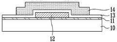
도 1은 본 발명에 따른 박막 트랜지스터를 설명하기 위한 단면도이다.1 is a cross-sectional view illustrating a thin film transistor according to the present invention.
도 1을 참조하면, 기판(10) 상에 버퍼층(11)이 형성되고, 버퍼층(11) 상에 제 1 게이트 전극(12)이 형성된다. 제 1 게이트 전극(12)을 포함하는 상부에는 게이트 절연막(13)이 형성되고, 제 1 게이트 전극(12)을 포함하는 게이트 절연막(13) 상에는 산화물 반도체로 활성층(14)이 형성된다. 활성층(14)은 채널 영역, 소스 영역 및 드레인 영역을 포함하며, 채널 영역이 제 1 게이트 전극(12)과 중첩되도록 배치된다. 산화물 반도체로는 산화아연(ZnO)이 사용될 수 있으며, 산화아연(ZnO)에는 갈륨(Ga), 인듐(In), 스태늄(Sn), 지르코늄(Zr), 하프늄(Hf) 및 바나듐(V) 중 적어도 하나의 이온이 도핑될 수 있다.Referring to FIG. 1, a
또한, 활성층(14)을 포함하는 상부에는 보호층(15)이 형성되고, 보호층(15) 상에는 소스 및 드레인 영역의 활성층(14)과 연결되는 소스 전극 및 드레인 전극(16a 및 16b)과, 소스 전극 및 드레인 전극(16a 및 16b) 사이에 배치되는 제 2 게이트 전극(16c)이 형성된다. 소스 및 드레인 전극(16a 및 16b)은 보호층(15)에 형성된 콘택홀을 통해 소스 및 드레인 영역의 활성층(14)에 연결되고, 제 2 게이트 전극(16c)과 소정 거리 이격된다. 제 2 게이트 전극(16c)은 제 1 게이트 전극(12)과 일부 또는 전부 중첩될 수 있다.In addition, a
상기와 같이 구성된 박막 트랜지스터의 제 1 게이트 전극(12) 및 제 2 게이트 전극(16c)에는 서로 동일하거나 서로 다른 바이어스 전압(VG)이 인가될 수 있다. 하나의 게이트 전극만을 구비하는 종래의 박막 트랜지스터는 게이트 전극에 바이어스 전압이 인가되면 게이트 전극과 인접하는 활성층의 일면에만 채널이 형성되지만, 본 발명의 박막 트랜지스터는 제 1 게이트 전극(12) 및 제 2 게이트 전극(16c)과 인접하는 활성층(14)의 양면에 채널이 형성되기 때문에 전류(on current) 특성이 종래 박막 트랜지스터에 비해 향상된다.The same or different bias voltages VG may be applied to the
도 2는 게이트 전압(VG)에 따른 드레인 전류(ID)의 변화(transfer curve)를 도시한 그래프이다. 종래의 박막 트랜지스터(점선 A)에 비해 본 발명의 박막 트랜지스터(실선 B)가 향상된 문턱전압(VTH) 특성을 가지는 것으로 측정되었다.FIG. 2 is a graph illustrating a transfer curve of the drain current ID according to the gate voltage VG. Compared with the conventional thin film transistor (dotted line A), the thin film transistor (solid line B) of the present invention was measured to have improved threshold voltage (VTH ) characteristics.
또한, 제 1 게이트 전극(12) 및 제 2 게이트 전극(16c)에 인가되는 바이어스 전압(VG)의 크기를 각각 조절하면 문턱전압(VTH)을 원하는 레벨로 용이하게 조절할 수 있다.In addition, by adjusting the magnitudes of the bias voltages VG applied to the
그러면 박막 트랜지스터의 제조 과정을 통해 본 발명을 보다 상세히 설명하기로 한다.Then, the present invention will be described in more detail through the manufacturing process of the thin film transistor.
도 3a 내지 도 3d는 본 발명에 따른 박막 트랜지스터의 제조 방법을 설명하 기 위한 단면도이다.3A to 3D are cross-sectional views illustrating a method of manufacturing a thin film transistor according to the present invention.
도 3a를 참조하면, 기판(10) 상에 버퍼층(11)을 형성한 후 버퍼층(11) 상에 제 1 게이트 전극(12)을 형성한다. 기판(10)으로는 실리콘(Si) 등의 반도체 기판, 유리나 플라스틱 등의 절연 기판 또는 금속 기판을 사용한다. 제 1 게이트 전극(12)은 Al, Cr, MoW 등의 금속으로 형성할 수 있다.Referring to FIG. 3A, after forming the
도 3b를 참조하면, 제 1 게이트 전극(12)을 포함하는 상부에 게이트 절연막(13)을 형성한다. 그리고 제 1 게이트 전극(12)을 포함하는 게이트 절연막(13) 상에 산화물 반도체층을 형성한 후 패터닝하여 채널 영역, 소스 영역 및 드레인 영역을 포함하는 활성층(14)을 형성한다. 이 때 채널 영역이 제 1 게이트 전극(12)과 중첩되도록 활성층(14)을 패터닝한다.Referring to FIG. 3B, a
게이트 절연막(13)은 실리콘 산화물(SiO), 실리콘 질화물(SiN) 등의 절연물로 형성한다. 산화물 반도체층은 산화아연(ZnO)으로 형성하거나, 갈륨(Ga), 인듐(In), 스태늄(Sn), 지르코늄(Zr), 하프늄(Hf) 및 바나듐(V) 중 적어도 하나의 이온이 도핑된 산화아연(ZnO) 예를 들어, ZnO, ZnGaO, ZnInO, ZnSnO, GaInZnO 등으로 형성한다.The
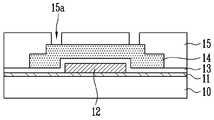
도 3c를 참조하면, 활성층(14)을 포함하는 상부에 보호층(15)을 형성하고 패터닝하여 활성층(14)의 소스 및 드레인 영역이 노출되도록 콘택홀(15a)을 형성한다.Referring to FIG. 3C, the
도 3d를 참조하면, 콘택홀(15a)이 매립되도록 보호층(15) 상에 Mo, MoW, Al, AlNd, AlLiLa 등으로 도전층을 형성하고 패터닝하여 콘택홀(15a)을 통해 소스 및 드레인 영역의 활성층(14)과 연결되는 소스 전극 및 드레인 전극(16a 및 16b)과, 소스 전극 및 드레인 전극(16a 및 16b) 사이에 배치되는 제 2 게이트 전극(16c)을 형성한다. 이 때 소스 전극 및 드레인 전극(16a 및 16b)은 제 2 게이트 전극(16c)과 소정 거리 이격되어 전기적으로 분리되도록 하고, 제 2 게이트 전극(16c)은 제 1 게이트 전극(12)과 일부 또는 전부 중첩되도록 한다.Referring to FIG. 3D, a conductive layer of Mo, MoW, Al, AlNd, AlLiLa, or the like is formed and patterned on the
상기 도전층을 패터닝하는 과정에서 보호층(15)을 식각 정지층(etch stop layer)으로 이용하면 식각 공정이 용이하고 활성층(14)의 손상이나 오염을 효과적으로 방지할 수 있다.If the
상기와 같이 구성된 본 발명의 박막 트랜지스터는 유기전계발광 표시 장치에 적용될 수 있다.The thin film transistor of the present invention configured as described above may be applied to an organic light emitting display device.
도 4a 및 도 4b는 본 발명에 따른 박막 트랜지스터를 구비하는 유기전계발광 표시 장치의 일 실시예를 설명하기 위한 평면도 및 단면도로서, 화상을 표시하는 표시 패널(200)을 중심으로 개략적으로 설명한다.4A and 4B are plan views and cross-sectional views illustrating an exemplary embodiment of an organic light emitting display device including a thin film transistor according to the present invention, and will be schematically described with reference to the
도 4a를 참조하면, 기판(210)은 화소 영역(220)과, 화소 영역(220) 주변의 비화소 영역(230)으로 정의된다. 화소 영역(220)의 기판(210)에는 주사 라인(224) 및 데이터 라인(226) 사이에 매트릭스 방식으로 연결된 다수의 유기전계발광 소자(300)가 형성되고, 비화소 영역(230)의 기판(210)에는 화소 영역(220)의 주사 라인(224) 및 데이터 라인(226)으로부터 연장된 주사 라인(224) 및 데이터 라인(226), 유기전계발광 소자(300)의 동작을 위한 전원공급 라인(도시안됨) 그리고 패드(228)를 통해 외부로부터 제공된 신호를 처리하여 주사 라인(224) 및 데이터 라인(226)으로 공급하는 주사 구동부(234) 및 데이터 구동부(236)가 형성된다.Referring to FIG. 4A, the
도 5를 참조하면, 유기전계발광 소자(300)는 애노드 전극(317) 및 캐소드 전극(320)과, 애노드 전극(317) 및 캐소드 전극(320) 사이에 형성된 유기 발광층(319)을 포함한다. 유기 발광층(319)은 정공 주입층, 정공 수송층, 전자 수송층 및 전자 주입층을 더 포함할 수 있다. 또한, 유기전계발광 소자(300)의 동작을 제어하기 위한 박막 트랜지스터 및 신호를 유지시키기 위한 캐패시터를 더 포함할 수 있다.Referring to FIG. 5, the organic light emitting
박막 트랜지스터는 도 1과 같은 구조를 가지며, 도 3a 내지 도 3d를 참조하여 설명한 본 발명의 제조 방법에 따라 제조될 수 있다.The thin film transistor has a structure as illustrated in FIG. 1 and may be manufactured according to the manufacturing method of the present invention described with reference to FIGS. 3A to 3D.
상기와 같이 구성된 박막 트랜지스터를 포함하는 유기전계발광 소자(300)를 도 4a 및 도 5를 통해 보다 상세히 설명하면 다음과 같다.The
기판(210) 상에 버퍼층(11)이 형성되고, 화소 영역(220)의 버퍼층(11) 상에 제 1 게이트 전극(12)이 형성된다. 이 때 화소 영역(220)에는 제 1 게이트 전극(12)과 연결되는 주사 라인(224)이 형성되고, 비화소 영역(230)에는 화소 영역(220)의 주사 라인(224)으로부터 연장되는 주사 라인(224) 및 외부로부터 신호를 제공받기 위한 패드(228)가 형성될 수 있다.The
제 1 게이트 전극(12)을 포함하는 상부에는 게이트 절연막(13)에 의해 제 1 게이트 전극(12)과 절연되며, 채널 영역, 소스 영역 및 드레인 영역을 포함하는 활성층(14)이 형성된다.The
활성층(14)을 포함하는 상부에는 보호층(15)이 형성되며, 보호층(15)에는 활 성층(14)의 소스 및 드레인 영역이 노출되도록 콘택홀이 형성된다. 보호층(15) 상에는 콘택홀을 통해 소스 및 드레인 영역의 활성층(14)과 접촉되는 소스 전극 및 드레인 전극(16a 및 16b)과, 소스 전극 및 드레인 전극(16a 및 16b) 사이에 배치되는 제 2 게이트 전극(16c)이 형성된다. 이 때 화소 영역(220)에는 소스 전극 및 드레인 전극(16a 및 16b)과 연결되는 데이터 라인(226)이 형성되고, 비화소 영역(230)에는 화소 영역(220)의 데이터 라인(226)으로부터 연장되는 데이터 라인(226) 및 외부로부터 신호를 제공받기 위한 패드(228)가 형성된다.The
소스 전극 및 드레인 전극(16a 및 16b)과 제 2 게이트 전극(16c)을 포함하는 상부에는 평탄화층(17)이 형성되고, 평탄화층(17)에는 소스 전극 또는 드레인 전극(16a 또는 16b)이 노출되도록 비아홀이 형성된다. 그리고 비아홀을 통해 소스 전극 또는 드레인 전극(16a 또는 16b)과 연결되는 애노드 전극(317)이 형성된다.The
애노드 전극(317)을 포함하는 평탄화층(17) 상에는 애노드 전극(317)의 일부 영역(발광 영역)이 노출되도록 화소 정의막(318)이 형성되고, 노출된 애노드 전극(317) 상에는 유기 발광층(319)이 형성된다. 그리고 유기 발광층(319)을 포함하는 화소 정의막(318) 상에는 캐소드 전극(320)이 형성된다.The
도 4b를 참조하면, 상기와 같이 유기전계발광 소자(300)가 형성된 기판(210) 상부에는 화소 영역(220)을 밀봉시키기 위한 봉지 기판(400)이 배치되며, 밀봉재(410)에 의해 봉지 기판(400)이 기판(210)에 합착되어 표시 패널(200)이 완성된다.Referring to FIG. 4B, an
이상에서와 같이 상세한 설명과 도면을 통해 본 발명의 최적 실시예를 개시 하였다. 용어들은 단지 본 발명을 설명하기 위한 목적에서 사용된 것이지 의미 한정이나 특허청구범위에 기재된 본 발명의 범위를 제한하기 위하여 사용된 것은 아니다. 그러므로 본 기술 분야의 통상의 지식을 가진 자라면 이로부터 다양한 변형 및 균등한 타 실시예가 가능하다는 점을 이해할 것이다. 따라서 본 발명의 진정한 기술적 보호 범위는 첨부된 특허청구범위의 기술적 사상에 의해 정해져야 할 것이다.As described above, the optimum embodiment of the present invention has been disclosed through the detailed description and the drawings. The terms are used only for the purpose of describing the present invention and are not used to limit the scope of the present invention as defined in the meaning or claims. Therefore, those skilled in the art will understand that various modifications and equivalent other embodiments are possible from this. Therefore, the true technical protection scope of the present invention will be defined by the technical spirit of the appended claims.
도 1은 본 발명의 박막 트랜지스터를 설명하기 위한 단면도.1 is a cross-sectional view illustrating a thin film transistor of the present invention.
도 2는 게이트 전압(VG)에 따른 드레인 전류(ID)의 변화(transfer curve)를 도시한 그래프.2 is a graph showing a transfer curve of the drain current ID according to the gate voltage VG.
도 3a 내지 도 3d는 본 발명에 따른 박막 트랜지스터의 제조 방법을 설명하기 위한 단면도.3A to 3D are cross-sectional views illustrating a method of manufacturing a thin film transistor according to the present invention.
도 4a 및 도 4b는 본 발명에 따른 박막 트랜지스터를 구비하는 유기전계발광 표시 장치의 일 실시예를 설명하기 위한 평면도 및 단면도.4A and 4B are a plan view and a cross-sectional view for explaining an embodiment of an organic light emitting display device having a thin film transistor according to the present invention.
도 5는 도 4a의 유기전계발광 소자를 설명하기 위한 단면도.FIG. 5 is a cross-sectional view for describing the organic light emitting display device of FIG. 4A. FIG.
<도면의 주요 부분에 대한 부호의 설명><Explanation of symbols for the main parts of the drawings>
10, 210: 기판11: 버퍼층10, 210: substrate 11: buffer layer
12: 제 1 게이트 전극13: 게이트 절연막12: first gate electrode 13: gate insulating film
14: 활성층15: 보호층14: active layer 15: protective layer
15a: 콘택홀16a: 소스 전극15a:
16b: 드레인 전극17: 평탄화막16b: drain electrode 17: planarization film
200: 표시 패널220: 화소 영역200: display panel 220: pixel area
224: 주사 라인226: 데이터 라인224: scan line 226: data line
228: 패드230: 비화소 영역228: pad 230: non-pixel region
234: 주사 구동부236: 데이터 구동부234: scan driver 236: data driver
300: 유기전계발광 소자317: 애노드 전극300: organic electroluminescent device 317: anode electrode
318: 화소 정의막319: 유기 발광층318: pixel defining layer 319: organic light emitting layer
320: 캐소드 전극400: 봉지 기판320: cathode electrode 400: encapsulation substrate
410: 밀봉재410: sealing material
Claims (24)
Translated fromKoreanPriority Applications (4)
| Application Number | Priority Date | Filing Date | Title |
|---|---|---|---|
| KR1020090094561AKR20110037220A (en) | 2009-10-06 | 2009-10-06 | An organic light emitting display device comprising a thin film transistor, a method of manufacturing the same, and a thin film transistor |
| JP2010093032AJP2011082487A (en) | 2009-10-06 | 2010-04-14 | Thin-film transistor, method of manufacturing the same, and organic electric-field light-emitting display device having the same |
| US12/892,855US20110079784A1 (en) | 2009-10-06 | 2010-09-28 | Thin film transistor, method of manufacturing the thin film transistor and organic light emitting display device having thin film transistor |
| TW099133822ATW201117386A (en) | 2009-10-06 | 2010-10-05 | Thin film transistor, method of manufacturing the thin film transistor and organic light emitting display device having thin film transistor |
Applications Claiming Priority (1)
| Application Number | Priority Date | Filing Date | Title |
|---|---|---|---|
| KR1020090094561AKR20110037220A (en) | 2009-10-06 | 2009-10-06 | An organic light emitting display device comprising a thin film transistor, a method of manufacturing the same, and a thin film transistor |
Publications (1)
| Publication Number | Publication Date |
|---|---|
| KR20110037220Atrue KR20110037220A (en) | 2011-04-13 |
Family
ID=43822506
Family Applications (1)
| Application Number | Title | Priority Date | Filing Date |
|---|---|---|---|
| KR1020090094561ACeasedKR20110037220A (en) | 2009-10-06 | 2009-10-06 | An organic light emitting display device comprising a thin film transistor, a method of manufacturing the same, and a thin film transistor |
Country Status (4)
| Country | Link |
|---|---|
| US (1) | US20110079784A1 (en) |
| JP (1) | JP2011082487A (en) |
| KR (1) | KR20110037220A (en) |
| TW (1) | TW201117386A (en) |
Cited By (16)
| Publication number | Priority date | Publication date | Assignee | Title |
|---|---|---|---|---|
| US8737109B2 (en) | 2010-08-27 | 2014-05-27 | Semiconductor Energy Laboratory Co., Ltd. | Memory device and semiconductor device |
| WO2014200190A1 (en)* | 2013-06-11 | 2014-12-18 | 경희대학교 산학협력단 | Oxide semiconductor transistor used as pixel element of display device and manufacturing method therefor |
| KR20150050637A (en)* | 2013-10-29 | 2015-05-11 | 삼성디스플레이 주식회사 | Display device and manufacturing method thereof |
| US9029863B2 (en) | 2012-04-20 | 2015-05-12 | Semiconductor Energy Laboratory Co., Ltd. | Semiconductor device and method for manufacturing the same |
| US9147719B2 (en) | 2013-11-05 | 2015-09-29 | Samsung Display Co., Ltd. | Thin film transistor array substrate, organic light-emitting display apparatus and method of manufacturing the thin film transistor array substrate |
| KR20160093132A (en)* | 2015-01-28 | 2016-08-08 | 엘지디스플레이 주식회사 | Organic light emitting diode and organic light emitting diode display device having the same |
| KR20160120838A (en)* | 2015-04-08 | 2016-10-19 | 삼성디스플레이 주식회사 | Thin film transistor display panel and manufacturing method thereof |
| US9508749B2 (en) | 2013-10-14 | 2016-11-29 | Samsung Display Co., Ltd. | Display substrates and methods of manufacturing display substrates |
| KR20170026720A (en)* | 2015-08-27 | 2017-03-09 | 삼성디스플레이 주식회사 | Liquid crystal display device |
| KR20170098886A (en)* | 2015-01-21 | 2017-08-30 | 가부시키가이샤 재팬 디스프레이 | Display device |
| CN107342296A (en)* | 2016-05-02 | 2017-11-10 | 三星显示有限公司 | Semiconductor device and the display device including the semiconductor device |
| KR20180015659A (en)* | 2015-06-04 | 2018-02-13 | 쿤산 뉴 플랫 패널 디스플레이 테크놀로지 센터 씨오., 엘티디. | Thin film transistor and manufacturing method thereof |
| KR20180026610A (en)* | 2016-09-02 | 2018-03-13 | 삼성디스플레이 주식회사 | Display device and manufacturing method of the same |
| US9947798B2 (en) | 2014-07-23 | 2018-04-17 | Japan Display Inc. | Display device |
| US10347704B2 (en) | 2016-10-14 | 2019-07-09 | Samsung Display Co., Ltd. | Organic light-emitting display device |
| KR20230020583A (en)* | 2013-12-27 | 2023-02-10 | 가부시키가이샤 한도오따이 에네루기 켄큐쇼 | Semiconductor device |
Families Citing this family (35)
| Publication number | Priority date | Publication date | Assignee | Title |
|---|---|---|---|---|
| KR101812683B1 (en)* | 2009-10-21 | 2017-12-27 | 가부시키가이샤 한도오따이 에네루기 켄큐쇼 | Method for manufacturing semiconductor device |
| CN102870220B (en)* | 2010-04-30 | 2014-05-07 | 夏普株式会社 | Circuit board and display device |
| WO2012029596A1 (en)* | 2010-09-03 | 2012-03-08 | Semiconductor Energy Laboratory Co., Ltd. | Method for manufacturing semiconductor device |
| JP5275523B2 (en)* | 2010-11-04 | 2013-08-28 | シャープ株式会社 | Display device, semiconductor device, and display device manufacturing method |
| US9024317B2 (en) | 2010-12-24 | 2015-05-05 | Semiconductor Energy Laboratory Co., Ltd. | Semiconductor circuit, method for driving the same, storage device, register circuit, display device, and electronic device |
| TWI743509B (en) | 2011-05-05 | 2021-10-21 | 日商半導體能源研究所股份有限公司 | Semiconductor device and method for manufacturing the same |
| JP2013012610A (en)* | 2011-06-29 | 2013-01-17 | Dainippon Printing Co Ltd | Thin film transistor and manufacturing method of the same |
| US8836626B2 (en) | 2011-07-15 | 2014-09-16 | Semiconductor Energy Laboratory Co., Ltd. | Semiconductor device and method for driving the same |
| US9660092B2 (en) | 2011-08-31 | 2017-05-23 | Semiconductor Energy Laboratory Co., Ltd. | Oxide semiconductor thin film transistor including oxygen release layer |
| KR20130043063A (en) | 2011-10-19 | 2013-04-29 | 가부시키가이샤 한도오따이 에네루기 켄큐쇼 | Semiconductor device and manufacturing method thereof |
| TWI470810B (en) | 2012-09-21 | 2015-01-21 | E Ink Holdings Inc | Thin film transistor, array substrate and display device |
| KR20140061030A (en)* | 2012-11-13 | 2014-05-21 | 삼성디스플레이 주식회사 | Thin film transistor array panel and method for manufacturing thereof |
| JP6121149B2 (en)* | 2012-11-28 | 2017-04-26 | 富士フイルム株式会社 | Oxide semiconductor element, manufacturing method of oxide semiconductor element, display device, and image sensor |
| JP2014187181A (en)* | 2013-03-22 | 2014-10-02 | Toshiba Corp | Semiconductor device and manufacturing method of the same |
| CN103219463B (en)* | 2013-04-08 | 2015-09-02 | 上海和辉光电有限公司 | Organic electronic light emitting device and manufacture method thereof |
| JP6662432B2 (en)* | 2013-06-28 | 2020-03-11 | 株式会社リコー | Field effect transistor, display element, image display device and system |
| US10529740B2 (en) | 2013-07-25 | 2020-01-07 | Semiconductor Energy Laboratory Co., Ltd. | Semiconductor device including semiconductor layer and conductive layer |
| US9577110B2 (en)* | 2013-12-27 | 2017-02-21 | Semiconductor Energy Laboratory Co., Ltd. | Semiconductor device including an oxide semiconductor and the display device including the semiconductor device |
| KR102319478B1 (en)* | 2014-03-18 | 2021-10-29 | 삼성디스플레이 주식회사 | Thin film transistor array panel and manufacturing method thereof |
| CN105304719B (en)* | 2014-07-18 | 2020-04-14 | 上海和辉光电有限公司 | Flexible thin film transistor and method of manufacturing the same |
| KR20160013430A (en)* | 2014-07-25 | 2016-02-04 | 삼성디스플레이 주식회사 | Thin film transsistor and display apparatus having the same |
| TW201611298A (en)* | 2014-09-12 | 2016-03-16 | 中華映管股份有限公司 | Double film transistor and manufacturing method thereof |
| JP6618779B2 (en)* | 2014-11-28 | 2019-12-11 | 株式会社半導体エネルギー研究所 | Semiconductor device |
| KR102276118B1 (en)* | 2014-11-28 | 2021-07-13 | 삼성디스플레이 주식회사 | Thin film transistor and organic light emitting diode display including the same |
| CN104465787B (en)* | 2014-12-31 | 2017-10-17 | 京东方科技集团股份有限公司 | A kind of thin film transistor (TFT) and circuit structure |
| KR20160086016A (en)* | 2015-01-08 | 2016-07-19 | 삼성디스플레이 주식회사 | Thin film transistor array panel and manufacturing method therfor |
| TWI567950B (en)* | 2015-01-08 | 2017-01-21 | 群創光電股份有限公司 | Display panel |
| JPWO2016139828A1 (en)* | 2015-03-03 | 2017-04-27 | 株式会社東芝 | Semiconductor device |
| CN106298952B (en)* | 2015-06-04 | 2023-05-02 | 昆山工研院新型平板显示技术中心有限公司 | A kind of OLED device |
| SG10201701689UA (en) | 2016-03-18 | 2017-10-30 | Semiconductor Energy Lab | Semiconductor device, semiconductor wafer, and electronic device |
| US10217678B2 (en)* | 2016-06-14 | 2019-02-26 | Innolux Corporation | Display device and method of manufacturing the display device |
| KR102768407B1 (en)* | 2016-08-29 | 2025-02-18 | 삼성디스플레이 주식회사 | Display apparatus and method of manufacturing the same |
| CN106252362B (en)* | 2016-08-31 | 2019-07-12 | 深圳市华星光电技术有限公司 | A kind of array substrate and preparation method thereof |
| KR102431929B1 (en)* | 2017-10-31 | 2022-08-12 | 엘지디스플레이 주식회사 | Display Device And Method for Manufacturing Of The Same |
| WO2024000494A1 (en)* | 2022-06-30 | 2024-01-04 | 京东方科技集团股份有限公司 | Display substrate, preparation method therefor, and display apparatus |
Family Cites Families (11)
| Publication number | Priority date | Publication date | Assignee | Title |
|---|---|---|---|---|
| US5124769A (en)* | 1990-03-02 | 1992-06-23 | Nippon Telegraph And Telephone Corporation | Thin film transistor |
| JP3535307B2 (en)* | 1996-03-15 | 2004-06-07 | 株式会社半導体エネルギー研究所 | Semiconductor device |
| KR100601374B1 (en)* | 2004-05-28 | 2006-07-13 | 삼성에스디아이 주식회사 | A thin film transistor, a method of manufacturing the same, and a flat panel display device including the thin film transistor |
| US7247529B2 (en)* | 2004-08-30 | 2007-07-24 | Semiconductor Energy Laboratory Co., Ltd. | Method for manufacturing display device |
| JP4850457B2 (en)* | 2005-09-06 | 2012-01-11 | キヤノン株式会社 | Thin film transistor and thin film diode |
| JP4977478B2 (en)* | 2006-01-21 | 2012-07-18 | 三星電子株式会社 | ZnO film and method of manufacturing TFT using the same |
| JP2008042043A (en)* | 2006-08-09 | 2008-02-21 | Hitachi Ltd | Display device |
| JP5305630B2 (en)* | 2006-12-05 | 2013-10-02 | キヤノン株式会社 | Manufacturing method of bottom gate type thin film transistor and manufacturing method of display device |
| JP5245287B2 (en)* | 2007-05-18 | 2013-07-24 | ソニー株式会社 | Semiconductor device manufacturing method, thin film transistor substrate manufacturing method, and display device manufacturing method |
| JP5264197B2 (en)* | 2008-01-23 | 2013-08-14 | キヤノン株式会社 | Thin film transistor |
| US8187919B2 (en)* | 2008-10-08 | 2012-05-29 | Lg Display Co. Ltd. | Oxide thin film transistor and method of fabricating the same |
- 2009
- 2009-10-06KRKR1020090094561Apatent/KR20110037220A/ennot_activeCeased
- 2010
- 2010-04-14JPJP2010093032Apatent/JP2011082487A/enactivePending
- 2010-09-28USUS12/892,855patent/US20110079784A1/ennot_activeAbandoned
- 2010-10-05TWTW099133822Apatent/TW201117386A/enunknown
Cited By (30)
| Publication number | Priority date | Publication date | Assignee | Title |
|---|---|---|---|---|
| US10297322B2 (en) | 2010-08-27 | 2019-05-21 | Semiconductor Energy Laboratory Co., Ltd. | Memory device with a driving circuit comprising transistors each having two gate electrodes and an oxide semiconductor layer |
| US9449706B2 (en) | 2010-08-27 | 2016-09-20 | Semiconductor Energy Laboratory Co., Ltd. | Driving method for a semiconductor device with an oxide semiconductor layer between two gate electrodes |
| US8737109B2 (en) | 2010-08-27 | 2014-05-27 | Semiconductor Energy Laboratory Co., Ltd. | Memory device and semiconductor device |
| US9570593B2 (en) | 2012-04-20 | 2017-02-14 | Semiconductor Energy Laboratory Co., Ltd. | Semiconductor device and method for manufacturing the same |
| US9029863B2 (en) | 2012-04-20 | 2015-05-12 | Semiconductor Energy Laboratory Co., Ltd. | Semiconductor device and method for manufacturing the same |
| WO2014200190A1 (en)* | 2013-06-11 | 2014-12-18 | 경희대학교 산학협력단 | Oxide semiconductor transistor used as pixel element of display device and manufacturing method therefor |
| US9825058B2 (en) | 2013-06-11 | 2017-11-21 | University-Industry Cooperation Group Of Kyung Hee University | Oxide semiconductor transistor used as pixel element of display device and manufacturing method therefor |
| US9508749B2 (en) | 2013-10-14 | 2016-11-29 | Samsung Display Co., Ltd. | Display substrates and methods of manufacturing display substrates |
| KR20150050637A (en)* | 2013-10-29 | 2015-05-11 | 삼성디스플레이 주식회사 | Display device and manufacturing method thereof |
| US9147719B2 (en) | 2013-11-05 | 2015-09-29 | Samsung Display Co., Ltd. | Thin film transistor array substrate, organic light-emitting display apparatus and method of manufacturing the thin film transistor array substrate |
| US12142688B2 (en) | 2013-12-27 | 2024-11-12 | Semiconductor Energy Laboratory Co., Ltd. | Semiconductor device |
| US11757041B2 (en) | 2013-12-27 | 2023-09-12 | Semiconductor Energy Laboratory Co., Ltd. | Semiconductor device |
| KR20230020583A (en)* | 2013-12-27 | 2023-02-10 | 가부시키가이샤 한도오따이 에네루기 켄큐쇼 | Semiconductor device |
| US9947798B2 (en) | 2014-07-23 | 2018-04-17 | Japan Display Inc. | Display device |
| KR20170098886A (en)* | 2015-01-21 | 2017-08-30 | 가부시키가이샤 재팬 디스프레이 | Display device |
| US10283643B2 (en) | 2015-01-21 | 2019-05-07 | Japan Display Inc. | Display device |
| KR20160093132A (en)* | 2015-01-28 | 2016-08-08 | 엘지디스플레이 주식회사 | Organic light emitting diode and organic light emitting diode display device having the same |
| KR20160120838A (en)* | 2015-04-08 | 2016-10-19 | 삼성디스플레이 주식회사 | Thin film transistor display panel and manufacturing method thereof |
| KR20180015659A (en)* | 2015-06-04 | 2018-02-13 | 쿤산 뉴 플랫 패널 디스플레이 테크놀로지 센터 씨오., 엘티디. | Thin film transistor and manufacturing method thereof |
| US10665725B2 (en) | 2015-06-04 | 2020-05-26 | Kunshan New Flat Panel Display Technology Center Co., Ltd. | Thin film transistor |
| KR20170026720A (en)* | 2015-08-27 | 2017-03-09 | 삼성디스플레이 주식회사 | Liquid crystal display device |
| KR20170124672A (en)* | 2016-05-02 | 2017-11-13 | 삼성디스플레이 주식회사 | Semiconductor device and Display apparatus employing the same |
| CN107342296B (en)* | 2016-05-02 | 2023-08-11 | 三星显示有限公司 | Semiconductor device and display device including the same |
| CN107342296A (en)* | 2016-05-02 | 2017-11-10 | 三星显示有限公司 | Semiconductor device and the display device including the semiconductor device |
| KR20180026610A (en)* | 2016-09-02 | 2018-03-13 | 삼성디스플레이 주식회사 | Display device and manufacturing method of the same |
| KR20220053537A (en)* | 2016-09-02 | 2022-04-29 | 삼성디스플레이 주식회사 | Display device and manufacturing method of the same |
| US11575100B2 (en) | 2016-09-02 | 2023-02-07 | Samsung Display Co., Ltd. | Display device and method of manufacturing the same |
| US11871596B2 (en) | 2016-09-02 | 2024-01-09 | Samsung Display Co., Ltd. | Display device and method of manufacturing the same |
| US12256593B2 (en) | 2016-09-02 | 2025-03-18 | Samsung Display Co., Ltd. | Display device and method of manufacturing the same |
| US10347704B2 (en) | 2016-10-14 | 2019-07-09 | Samsung Display Co., Ltd. | Organic light-emitting display device |
Also Published As
| Publication number | Publication date |
|---|---|
| TW201117386A (en) | 2011-05-16 |
| JP2011082487A (en) | 2011-04-21 |
| US20110079784A1 (en) | 2011-04-07 |
Similar Documents
| Publication | Publication Date | Title |
|---|---|---|
| KR20110037220A (en) | An organic light emitting display device comprising a thin film transistor, a method of manufacturing the same, and a thin film transistor | |
| KR100941850B1 (en) | Thin film transistor, its manufacturing method, and flat panel display device comprising thin film transistor | |
| KR100975204B1 (en) | Thin film transistor, its manufacturing method, and flat panel display device comprising thin film transistor | |
| KR100963104B1 (en) | Thin film transistor, its manufacturing method, and flat panel display device comprising thin film transistor | |
| KR101064402B1 (en) | A flat panel display comprising a thin film transistor, a method of manufacturing the same, and a thin film transistor | |
| KR101056229B1 (en) | An organic light emitting display device comprising a thin film transistor, a method of manufacturing the same, and a thin film transistor | |
| KR100963027B1 (en) | Thin film transistor, its manufacturing method, and flat panel display device comprising thin film transistor | |
| KR101073301B1 (en) | Organic Light emitting Display device and fabrication method thereof | |
| KR100963003B1 (en) | Thin film transistor, its manufacturing method, and flat panel display device comprising thin film transistor | |
| KR100993416B1 (en) | A flat panel display comprising a thin film transistor, a method of manufacturing the same, and a thin film transistor | |
| KR101048965B1 (en) | Organic electroluminescent display | |
| KR100936874B1 (en) | Method for manufacturing thin film transistor and method for manufacturing organic light emitting display device comprising thin film transistor | |
| KR101034686B1 (en) | Organic light emitting display device and manufacturing method thereof | |
| KR100963026B1 (en) | Thin film transistor, its manufacturing method, and flat panel display device comprising thin film transistor | |
| KR20090124527A (en) | Thin film transistor, its manufacturing method, and flat panel display device comprising thin film transistor | |
| KR100958006B1 (en) | Thin film transistor, its manufacturing method, and flat panel display device comprising thin film transistor | |
| KR101048996B1 (en) | Thin film transistor and flat panel display having same | |
| KR100936871B1 (en) | Organic light emitting display device and manufacturing method thereof | |
| KR20090105561A (en) | Semiconductor device and flat panel display device having same | |
| KR101064442B1 (en) | Organic light emitting display | |
| KR101064470B1 (en) | Thin film transistor and its manufacturing method | |
| KR101022141B1 (en) | An organic light emitting display device comprising a thin film transistor, a method of manufacturing the same, and a thin film transistor | |
| KR100962989B1 (en) | Thin film transistor, its manufacturing method, and flat panel display device comprising thin film transistor | |
| KR101101034B1 (en) | A thin film transistor and an organic light emitting display device having the same | |
| KR100941855B1 (en) | Thin film transistor, its manufacturing method, and flat panel display device comprising thin film transistor |
Legal Events
| Date | Code | Title | Description |
|---|---|---|---|
| A201 | Request for examination | ||
| PA0109 | Patent application | Patent event code:PA01091R01D Comment text:Patent Application Patent event date:20091006 | |
| PA0201 | Request for examination | ||
| E902 | Notification of reason for refusal | ||
| PE0902 | Notice of grounds for rejection | Comment text:Notification of reason for refusal Patent event date:20110222 Patent event code:PE09021S01D | |
| PG1501 | Laying open of application | ||
| E601 | Decision to refuse application | ||
| PE0601 | Decision on rejection of patent | Patent event date:20110511 Comment text:Decision to Refuse Application Patent event code:PE06012S01D Patent event date:20110222 Comment text:Notification of reason for refusal Patent event code:PE06011S01I |