KR20110031466A - Gas Distribution Showerhead Skirt - Google Patents
Gas Distribution Showerhead SkirtDownload PDFInfo
- Publication number
- KR20110031466A KR20110031466AKR1020117001095AKR20117001095AKR20110031466AKR 20110031466 AKR20110031466 AKR 20110031466AKR 1020117001095 AKR1020117001095 AKR 1020117001095AKR 20117001095 AKR20117001095 AKR 20117001095AKR 20110031466 AKR20110031466 AKR 20110031466A
- Authority
- KR
- South Korea
- Prior art keywords
- gas distribution
- distribution showerhead
- showerhead
- skirt
- susceptor
- Prior art date
- Legal status (The legal status is an assumption and is not a legal conclusion. Google has not performed a legal analysis and makes no representation as to the accuracy of the status listed.)
- Withdrawn
Links
- 238000009826distributionMethods0.000titleclaimsabstractdescription62
- 238000000034methodMethods0.000claimsabstractdescription29
- 239000000463materialSubstances0.000claimsabstractdescription16
- 238000000623plasma-assisted chemical vapour depositionMethods0.000claimsdescription13
- 238000011144upstream manufacturingMethods0.000claimsdescription6
- 239000000758substrateSubstances0.000abstractdescription44
- 230000008021depositionEffects0.000abstractdescription7
- 239000007789gasSubstances0.000description48
- 238000000151depositionMethods0.000description6
- 238000004140cleaningMethods0.000description3
- 238000009827uniform distributionMethods0.000description3
- 238000004519manufacturing processMethods0.000description2
- 239000013078crystalSubstances0.000description1
- -1for exampleSubstances0.000description1
- 239000011521glassSubstances0.000description1
- 239000012212insulatorSubstances0.000description1
- 230000003993interactionEffects0.000description1
- 239000007769metal materialSubstances0.000description1
- 230000000149penetrating effectEffects0.000description1
- 239000002243precursorSubstances0.000description1
- 239000004065semiconductorSubstances0.000description1
- 229910001220stainless steelInorganic materials0.000description1
- 239000010935stainless steelSubstances0.000description1
- 235000012431wafersNutrition0.000description1
Images


Classifications
- C—CHEMISTRY; METALLURGY
- C23—COATING METALLIC MATERIAL; COATING MATERIAL WITH METALLIC MATERIAL; CHEMICAL SURFACE TREATMENT; DIFFUSION TREATMENT OF METALLIC MATERIAL; COATING BY VACUUM EVAPORATION, BY SPUTTERING, BY ION IMPLANTATION OR BY CHEMICAL VAPOUR DEPOSITION, IN GENERAL; INHIBITING CORROSION OF METALLIC MATERIAL OR INCRUSTATION IN GENERAL
- C23C—COATING METALLIC MATERIAL; COATING MATERIAL WITH METALLIC MATERIAL; SURFACE TREATMENT OF METALLIC MATERIAL BY DIFFUSION INTO THE SURFACE, BY CHEMICAL CONVERSION OR SUBSTITUTION; COATING BY VACUUM EVAPORATION, BY SPUTTERING, BY ION IMPLANTATION OR BY CHEMICAL VAPOUR DEPOSITION, IN GENERAL
- C23C16/00—Chemical coating by decomposition of gaseous compounds, without leaving reaction products of surface material in the coating, i.e. chemical vapour deposition [CVD] processes
- C23C16/44—Chemical coating by decomposition of gaseous compounds, without leaving reaction products of surface material in the coating, i.e. chemical vapour deposition [CVD] processes characterised by the method of coating
- C23C16/50—Chemical coating by decomposition of gaseous compounds, without leaving reaction products of surface material in the coating, i.e. chemical vapour deposition [CVD] processes characterised by the method of coating using electric discharges
- C23C16/505—Chemical coating by decomposition of gaseous compounds, without leaving reaction products of surface material in the coating, i.e. chemical vapour deposition [CVD] processes characterised by the method of coating using electric discharges using radio frequency discharges
- C23C16/509—Chemical coating by decomposition of gaseous compounds, without leaving reaction products of surface material in the coating, i.e. chemical vapour deposition [CVD] processes characterised by the method of coating using electric discharges using radio frequency discharges using internal electrodes
- C23C16/5096—Flat-bed apparatus
- C—CHEMISTRY; METALLURGY
- C23—COATING METALLIC MATERIAL; COATING MATERIAL WITH METALLIC MATERIAL; CHEMICAL SURFACE TREATMENT; DIFFUSION TREATMENT OF METALLIC MATERIAL; COATING BY VACUUM EVAPORATION, BY SPUTTERING, BY ION IMPLANTATION OR BY CHEMICAL VAPOUR DEPOSITION, IN GENERAL; INHIBITING CORROSION OF METALLIC MATERIAL OR INCRUSTATION IN GENERAL
- C23C—COATING METALLIC MATERIAL; COATING MATERIAL WITH METALLIC MATERIAL; SURFACE TREATMENT OF METALLIC MATERIAL BY DIFFUSION INTO THE SURFACE, BY CHEMICAL CONVERSION OR SUBSTITUTION; COATING BY VACUUM EVAPORATION, BY SPUTTERING, BY ION IMPLANTATION OR BY CHEMICAL VAPOUR DEPOSITION, IN GENERAL
- C23C16/00—Chemical coating by decomposition of gaseous compounds, without leaving reaction products of surface material in the coating, i.e. chemical vapour deposition [CVD] processes
- C23C16/44—Chemical coating by decomposition of gaseous compounds, without leaving reaction products of surface material in the coating, i.e. chemical vapour deposition [CVD] processes characterised by the method of coating
- C23C16/455—Chemical coating by decomposition of gaseous compounds, without leaving reaction products of surface material in the coating, i.e. chemical vapour deposition [CVD] processes characterised by the method of coating characterised by the method used for introducing gases into reaction chamber or for modifying gas flows in reaction chamber
- C23C16/45563—Gas nozzles
- C23C16/45565—Shower nozzles
- C—CHEMISTRY; METALLURGY
- C23—COATING METALLIC MATERIAL; COATING MATERIAL WITH METALLIC MATERIAL; CHEMICAL SURFACE TREATMENT; DIFFUSION TREATMENT OF METALLIC MATERIAL; COATING BY VACUUM EVAPORATION, BY SPUTTERING, BY ION IMPLANTATION OR BY CHEMICAL VAPOUR DEPOSITION, IN GENERAL; INHIBITING CORROSION OF METALLIC MATERIAL OR INCRUSTATION IN GENERAL
- C23C—COATING METALLIC MATERIAL; COATING MATERIAL WITH METALLIC MATERIAL; SURFACE TREATMENT OF METALLIC MATERIAL BY DIFFUSION INTO THE SURFACE, BY CHEMICAL CONVERSION OR SUBSTITUTION; COATING BY VACUUM EVAPORATION, BY SPUTTERING, BY ION IMPLANTATION OR BY CHEMICAL VAPOUR DEPOSITION, IN GENERAL
- C23C16/00—Chemical coating by decomposition of gaseous compounds, without leaving reaction products of surface material in the coating, i.e. chemical vapour deposition [CVD] processes
- C23C16/44—Chemical coating by decomposition of gaseous compounds, without leaving reaction products of surface material in the coating, i.e. chemical vapour deposition [CVD] processes characterised by the method of coating
- C23C16/455—Chemical coating by decomposition of gaseous compounds, without leaving reaction products of surface material in the coating, i.e. chemical vapour deposition [CVD] processes characterised by the method of coating characterised by the method used for introducing gases into reaction chamber or for modifying gas flows in reaction chamber
- C23C16/45587—Mechanical means for changing the gas flow
- H—ELECTRICITY
- H01—ELECTRIC ELEMENTS
- H01J—ELECTRIC DISCHARGE TUBES OR DISCHARGE LAMPS
- H01J37/00—Discharge tubes with provision for introducing objects or material to be exposed to the discharge, e.g. for the purpose of examination or processing thereof
- H01J37/32—Gas-filled discharge tubes
- H01J37/32431—Constructional details of the reactor
- H01J37/3244—Gas supply means
Landscapes
- Chemical & Material Sciences (AREA)
- Engineering & Computer Science (AREA)
- General Chemical & Material Sciences (AREA)
- Chemical Kinetics & Catalysis (AREA)
- Materials Engineering (AREA)
- Mechanical Engineering (AREA)
- Metallurgy (AREA)
- Organic Chemistry (AREA)
- Physics & Mathematics (AREA)
- Plasma & Fusion (AREA)
- Analytical Chemistry (AREA)
- Chemical Vapour Deposition (AREA)
Abstract
Translated fromKoreanDescription
Translated fromKorean본 발명의 실시예들은 일반적으로 가스 분배 샤워헤드 또는 보조 전극으로부터 연장하는 연장부(extension)에 관한 것이다.
Embodiments of the present invention generally relate to an extension extending from a gas distribution showerhead or auxiliary electrode.
대형 평판형 디스플레이 패널에 대한 요구가 계속되면서, 제조 단계들 중의 일부 단계가 수행될 처리 챔버의 크기도 대형화되어야 한다. 평판형 디스플레이 패널의 제조에 사용되는 방법이 플라즈마 강화 화학 기상 증착(PECVD) 방법이라면, 하나 또는 그보다 많은 전구체 가스들이 처리 챔버 내측으로 유입되어서 기판 상에 층을 증착하도록 플라즈마로 점화된다. PECVD는 예를 들어, 반도체 웨이퍼, 평판형 디스플레이 기판, 및 태양전지 패널 기판을 포함한 다양한 형태의 기판 상에 층을 증착하는데 사용될 수 있다.As the demand for large flat panel displays continues, the size of the processing chamber in which some of the manufacturing steps will be performed must also be enlarged. If the method used in the manufacture of a flat panel display panel is a plasma enhanced chemical vapor deposition (PECVD) method, one or more precursor gases are introduced into the processing chamber and ignited with plasma to deposit a layer on the substrate. PECVD can be used to deposit layers on various types of substrates including, for example, semiconductor wafers, flat panel display substrates, and solar panel substrates.
PECVD에서, 처리 가스는 가스 분배 샤워헤드를 통해 처리 챔버의 내측으로 유입될 수 있다. 가스 분배 샤워헤드는 처리 가스를 플라즈마로 점화시키도록 전기적으로 바이어스될 수 있다. 따라서, 가스 분배 샤워헤드는 가스를 분배할 뿐만 아니라 플라즈마로 점화시키데 유리할 수 있다.In PECVD, process gas can be introduced into the process chamber through a gas distribution showerhead. The gas distribution showerhead may be electrically biased to ignite the process gas into the plasma. Thus, the gas distribution showerhead may be advantageous for distributing the gas as well as igniting it with plasma.
그러므로, 본 기술 분야에는 PECVD 챔버에 사용하기 위한 대형 가스 분배 샤워헤드가 필요하다.
Therefore, there is a need in the art for large gas distribution showerheads for use in PECVD chambers.
본 발명은 일반적으로 처리 챔버 내의 가스 분배 샤워헤드로부터 연장하는 연장부 또는 스커트를 포함한다. 기판을 처리할 때, 가스 분배 샤워헤드는 전기적으로 바이어스될 수 있다. 전기적으로 바이어스된 샤워헤드는 몇몇 경우에, 처리 가스를 플라즈마 상태로 점화시킨다. 처리 챔버의 벽 및 서셉터는 샤워헤드에 대해 접지될 수 있다. 따라서, 기판의 에지들은 전기적으로 편향된 샤워헤드에 비해서 커다란 표면적의 접지 접점을 가질 수 있다. 에지 근처에서 접지(grounding)의 증가로 인해, 기판 상에 증착된 재료가 기판 중앙부에 비해서 상이한 특성들을 가질 수 있다. 기판 쪽에 가깝게 아래로 샤워헤드 에지를 연장함으로써, 증착 재료의 실질적으로 균일한 특성들이 얻어질 수 있다.The present invention generally includes an extension or skirt extending from the gas distribution showerhead in the processing chamber. When processing the substrate, the gas distribution showerhead can be electrically biased. Electrically biased showerheads in some cases ignite the process gas into a plasma state. The wall of the processing chamber and the susceptor may be grounded to the showerhead. Thus, the edges of the substrate may have a large surface area ground contact as compared to the electrically deflected showerhead. Due to the increase in grounding near the edges, the material deposited on the substrate may have different properties compared to the center of the substrate. By extending the showerhead edge down closer to the substrate side, substantially uniform properties of the deposition material can be obtained.
일 실시예에서, 장치는 처리 챔버 몸체 및 상기 처리 챔버 몸체 내에 배열되는 가스 분배 샤워헤드를 포함한다. 상기 샤워헤드는 파워 소오스에 연결된다. 상기 장치는 또한, 상기 처리 챔버 몸체 내측에 배열되며 제 2 파워 소오스에 연결되는 보조 전극을 포함한다. 상기 장치는 또한, 상기 처리 챔버 몸체 내에 배열되며 상기 보조 전극 및 가스 분배 샤워헤드로부터 이격된 서셉터를 포함한다.In one embodiment, the apparatus includes a process chamber body and a gas distribution showerhead arranged within the process chamber body. The showerhead is connected to a power source. The apparatus also includes an auxiliary electrode arranged inside the processing chamber body and connected to a second power source. The apparatus also includes a susceptor arranged in the processing chamber body and spaced apart from the auxiliary electrode and a gas distribution showerhead.
다른 실시예에서, 가스 분배 샤워헤드는 상류 측과 하류 측을 가지며 상기 상류 측과 하류 측 사이로 연장하는 하나 또는 그보다 많은 가스 통로를 가지는 가스 분배 샤워헤드 몸체를 가진다. 상기 샤워헤드는 상기 하류 측으로부터 상기 상기 가스 분배 샤워헤드 몸체에 연결되고 상기 가스 분배 샤워헤드로부터 연장하는 하나 또는 그보다 많은 보조 전극을 포함한다.In another embodiment, the gas distribution showerhead has a gas distribution showerhead body having an upstream side and a downstream side and having one or more gas passageways extending between the upstream side and the downstream side. The showerhead includes one or more auxiliary electrodes connected to the gas distribution showerhead body from the downstream side and extending from the gas distribution showerhead.
다른 실시예에서, 플라즈마 강화 화학 기상 증착 장치는 처리 챔버 몸체와, 상기 처리 챔버 몸체 내에 배열되는 서셉터, 및 상기 처리 챔버 몸체 내에 배열되고 상기 서셉터로부터 분리되는 가스 분배 샤워헤드를 포함한다. 상기 가스 분배 샤워헤드는 상기 서셉터를 지향하는 하류 표면 및 상기 하류 표면과 반대편의 상류 표면을 가질 수 있다. 상기 장치는 또한, 상기 가스 분배 샤워헤드와 상기 서셉터 사이에 배열되는 하나 또는 그보다 많은 보조 전극을 포함한다. 하나 또는 그보다 많은 보조 전극은 파워 소오스에 연결된다.In another embodiment, a plasma enhanced chemical vapor deposition apparatus includes a processing chamber body, a susceptor arranged in the processing chamber body, and a gas distribution showerhead arranged in the processing chamber body and separated from the susceptor. The gas distribution showerhead may have a downstream surface that faces the susceptor and an upstream surface opposite the downstream surface. The apparatus also includes one or more auxiliary electrodes arranged between the gas distribution showerhead and the susceptor. One or more auxiliary electrodes are connected to the power source.
본 발명의 전술한 특징들이 구체적으로 이해될 수 있는 방식으로, 위에서 약술한 본 발명에 대해 몇몇 실시예들이 첨부 도면에 도시된 실시예들을 참조하여 더욱 더 구체적으로 설명될 것이다. 그러나, 첨부 도면들은 단지 본 발명의 전형적인 실시예들만을 도시한 것이므로 본 발명의 범주를 제한 것으로 생각해서는 안 되며 본 발명은 다른 균등한 효과적인 실시예들이 있을 수 있다는 것을 주목해야 한다.
In the manner in which the above-described features of the present invention can be specifically understood, some embodiments of the present invention outlined above will be described more specifically with reference to the embodiments shown in the accompanying drawings. It should be noted, however, that the appended drawings illustrate only typical embodiments of this invention and are therefore not to be considered limiting of its scope, for the invention may have other equivalent effective embodiments.
도 1a는 본 발명의 일 실시예에 따른 처리 장치(100)의 개략적인 횡단면도이며,
도 1b는 처리 위치에 기판(106)을 갖는 도 1a의 처리 장치(100)의 개략적인 횡단면도이며,
도 2a는 본 발명의 다른 실시예에 따른 처리 장치(200)의 개략적인 횡단면도이며,
도 2b는 처리 위치에 기판을 갖는 도 2a의 처리 장치(200)의 개략적인 횡단면도이며,
도 3은 본 발명의 일 실시예에 따른 가스 분배 샤워헤드(302) 및 스커트(304)의 개략적인 등각도이며,
도 4는 본 발명의 다른 실시예에 따른 가스 분배 샤워헤드(402) 및 스커트(404)의 개략적인 등각도이다.1A is a schematic cross-sectional view of a
FIG. 1B is a schematic cross sectional view of the
2A is a schematic cross-sectional view of a
FIG. 2B is a schematic cross sectional view of the
3 is a schematic isometric view of
4 is a schematic isometric view of
이해를 쉽게 하기 위해, 도면에서 공통인 동일한 구성 요소를 지칭하기 위해 가능한 동일한 참조 부호가 사용되었다. 일 실시예의 구성 요소와 특징들은 추가의 언급 없이도 다른 실시예에 유리하게 결합될 수 있다고 이해해야 한다.For ease of understanding, the same reference numerals have been used where possible to refer to the same components that are common in the figures. It is to be understood that the components and features of one embodiment may be advantageously combined with other embodiments without further recitation.
본 발명은 일반적으로 처리 챔버 내의 가스 분배 샤워헤드로부터 연장하는 연장부 또는 스커트를 포함한다. 기판을 처리할 때, 가스 분배 샤워헤드는 전기적으로 바이어스될 수 있다. 전기적으로 바이어스된 샤워헤드는 몇몇 경우에, 처리 가스를 플라즈마 상태로 점화시킬 수 있다. 처리 챔버의 벽 및 서셉터는 샤워헤드와는 상대적으로 접지될 수 있다. 따라서, 기판의 에지들이 전기적으로 바이어스된 샤워헤드에 비해서 상당히 큰 표면적의 접지 접점을 가질 수 있다. 상기 에지 근처에서의 접지의 증가로 인해, 기판 상에 증착되는 재료는 기판의 중간에 비해서 상이한 특징들을 가질 수 있다. 샤워헤드 에지를 기판 쪽에 가깝게 아래로 연장시킴으로써, 재료의 실질적으로 균일한 특성들이 얻어질 수 있다.The present invention generally includes an extension or skirt extending from the gas distribution showerhead in the processing chamber. When processing the substrate, the gas distribution showerhead can be electrically biased. The electrically biased showerhead may in some cases ignite the process gas into a plasma state. The wall and susceptor of the processing chamber may be grounded relative to the showerhead. Thus, the edges of the substrate may have a ground surface contact of significantly greater surface area compared to the electrically biased showerhead. Due to the increase in ground near the edge, the material deposited on the substrate may have different characteristics compared to the middle of the substrate. By extending the showerhead edge down closer to the substrate side, substantially uniform properties of the material can be obtained.
후술하는 바와 같이, 본 발명은 미국 캘리포니아 산타 클라라 소재의 어플라이드 머티리얼즈 인코포레이티드의 자회사인 에이케이티 어메리카로부터 이용가능한 PECVD 시스템에서 실시될 수 있다. 본 발명은 다른 제작자로부터 처리 챔버들을 포함한 다른 플라즈마 처리 챔버들에서 실시될 수 있다고 이해해야 한다.As described below, the present invention may be practiced in a PECVD system available from ACC America, a subsidiary of Applied Materials, Inc., Santa Clara, California. It should be understood that the present invention may be practiced in other plasma processing chambers, including processing chambers, from other manufacturers.
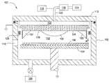
도 1a는 본 발명의 일 실시예에 따른 처리 장치(100)의 개략적인 횡단면도이다. 상기 처리 장치(100)는 처리 중에 기판을 지지하는 서셉터(104)를 에워싸는 챔버 몸체(102)를 포함할 수 있다. 상기 장치(100)는 진공 펌프(108)에 의해 배기될 수 있다. 상기 기판(106)은 슬릿 밸브 개구(110)를 통해 챔버 몸체(102)를 출입할 수 있다.1A is a schematic cross-sectional view of a
처리 가스는 가스 소오스(114)로부터 상기 장치(100)로 분배될 수 있다. 상기 가스 소오스(114)는 처리 가스뿐만 아니라 세정 가스를 제공할 수 있다. 처리 가스는 원격 플라즈마 소오스(116)로부터 가스 튜브(120)를 통해 상기 장치(100)로 이동한다. 상기 가스는 배면 판(112)을 통해 상기 장치(100)로 유입된다. 상기 장치(100)가 세정 필요성이 있을 때, 세정 가스는 가스 소오스(114)로부터 원격 플라즈마 소오스(116)로 분배되며 플라즈마로 점화될 수 있다. 일단 점화되면, 상기 플라즈마는 장치(100)로 분배될 수 있다.Process gas may be dispensed from the
파워 소오스(118)도 상기 장치(100)에 연결될 수 있다. 일 실시예에서, 파워 소오스(118)는 RF 전류를 분배하는 RF 파워 소오스를 포함할 수 있다. 파워 소오스(118)는 상기 장치(100) 내에 배열된 가스 분배 샤워헤드(124)로 파워를 분배할 수 있다. RF 전류용 RF 복귀 통로는 본 발명에 사용된 일반적인 용어 "접지"에 포함된다고 이해되어야 한다.A
가스 분배 샤워헤드(124)는 원격 생성된 플라즈마로부터의 처리 가스 및/또는 라디칼이 처리 영역(132)으로 통과할 수 있게 하기 위한, 샤워헤드를 관통하는 하나 또는 그보다 많은 가스 통로(126)를 가질 수 있다. 처리 가스가 배면 판(112)을 통해 상기 장치(100)로 유입될 때, 상기 가스는 배면 판(112)과 샤워헤드(124) 사이의 플레넘(122)으로 유입된다.The
서셉터(104)는 챔버 몸체(102)를 통해 접지될 수 있다. 기판(106)이 유리와 같은 절연 기판일 때, 서셉터(104)의 대부분은 덮이게 되나, 서셉터(104)의 에지들은 덮이지 않게 되며, 그로 인해 처리 중에 접지를 위한 통로를 제공한다. 추가로, 챔버 몸체(102)가 접지되기 때문에, 챔버 몸체(102)도 접지를 위한 통로를 제공한다. 챔버 몸체(102)는 처리 영역(132)을 에워싼다. 따라서, 서셉터(104)의 에지 및 챔버 몸체(102)에 가장 가까운 기판(106)의 영역들은 중심에 더 가까운 기판의 영역들보다 접지에 더 가깝다. 기판의 에지 및 코너들이 접지에 더 가깝기 때문에, 기판(106)은 균일하게 코팅될 수 없다. 기판(106)은 중앙에 비해서 기판(106)의 에지 및 코너 근처에서 상이한 두께를 갖는 증착 재료를 가질 수 있다. 또한, 기판(106)은 중앙에 비해서 기판(106)의 에지 및 코너 근처에서 결정 구조와 같은 상이한 필름 특성들을 가지는 증착 재료를 가질 수 있다. 그러한 불균일성은 장치(100) 내에 불균일한 플라즈마 분배에 의해 유발될 수 있다.The
처리 챔버 내에 플라즈마 분포를 균일하게 하기 위해, 샤워헤드(124)는 샤워헤드에 연결된 연장부 또는 스커트(130)를 가질 수 있다. 일 실시예에서, 상기 스커트(130)는 금속 재료를 포함할 수 있다. 다른 실시예에서, 스커트(130)는 스테인리스 스틸을 포함할 수 있다. 상기 스커트(130)는 샤워헤드(124)로부터 샤워헤드의 외측 에지를 따라 서셉터(104) 쪽으로 연장할 수 있다. 상기 스커트(130)는 샤워헤드(124)와 일체형인 단일 재료일 수 있다. 일 실시예에서, 상기 스커트(130)는 샤워헤드(124)에 연결되는 별도 부품을 포함할 수 있다. 스커트(130)는 샤워헤드(124)의 외측 주변부의 적어도 일부분을 따라 배열될 수 있으며 가스 통로(126)를 통과하는 어떤 가스와도 간섭되거나 어떤 가스를 차단하지 않는다. 스커트(130)가 샤워헤드(124)에 연결되기 때문에, 스커트(130)는 전기적으로 바이어스된다. 그러므로, 스커트(130)는 처리 중에 기판(106)의 외측 주변부 근처에 전극 표면을 제공한다. 전기적으로 바이어스된 스커트(130)의 존재로 필름 특성 및 두께를 포함한, 기판(106) 상의 균일한 증착을 허용할 수 있다. 접지된 절연기(128)가 스커트(130) 뒤의 챔버 몸체(102)에 연결될 수 있다.To homogenize the plasma distribution in the processing chamber, the
스커트(130)는 화살표 "A"로 나타낸 거리만큼 서섭터(104)로부터 이격될 수 있다. 처리 중에, 스커트(130)는 도 1b에 화살표 "B"로 나타낸 거리만큼 서셉터(104)로부터 이격될 수 있다. 스커트(130)는 챔버 몸체(102) 내에 추가의 전극 표면을 제공한다. 전극들로서 접지된 서셉터(104) 및 챔버 벽들은 표면적을 가진다. 스커트(130)는 샤워헤드(124)로부터 아래로 연장함으로써 처리 중에 플라즈마가 보이는 벽의 하나 또는 그보다 많은 부분들을 차단함으로써, 처리 중에 플라즈마가 보이거나 노출되는 애노드의 표면적을 감소시킨다. 그러므로, 전기적으로 바이어스된 스커트(130)는 접지된 서셉터(104)와 상호 작용함으로써 애노드 표면적을 감소시키고 접지에 대한 이용가능한 통로를 감소시킨다. 스커트(130)의 존재와 스커트(130)의 형상 및 스커트와 서셉터(104)와의 상호 작용은 플라즈마에 영향을 끼치며 그에 따라 기판(106) 상의 증착에 영향을 끼친다. 접지된 애노드는 플라즈마를 애노드로 당김으로써 기판(106)의 중심으로부터 더 멀어지게 한다. 전기적으로 바이어스된 스커트(130)는 플라즈마가 보이는 애노드 표면적을 감소시키며 중심으로부터 멀어지게 작은 양의 플라즈마를 당기는 경향이 있다. 그러므로, 스커트(130)의 형상 및 위치는 장치(100) 내의 플라즈마의 균일한 분포를 허용함으로써 기판(106) 상에 증착된 재료의 균일한 특성을 제공하도록 플라즈마를 형상화하도록 조절될 수 있다.The
스커트(130)의 존재는 장치(100)와 전기적으로 바이어스된 전극의 표면적을 증가시킨다. 따라서, 스커트(130)가 존재하지 않는 상황에 비해서, 전극의 표면적은 접지된 표면적에 비해 증가된다. 특히, 기판(106)의 에지 근처의 접지된 표면에 대한 기판의 에지 근처의 전극 표면의 비율은 증가된다. 따라서, 기판(106) 상에 증착된 재료는 특성 및 두께가 균일해질 수 있다.The presence of the
스커트(130)는 일 실시예에서 샤워헤드(124)의 선택된 부분들로부터 연장할 수 있다. 예를 들어, 스커트(130)는 도 1a 및 도 1b에 도시한 바와 같은 측면들의 중앙부 및 샤워헤드(124)의 코너(124)로부터 연장할 수 있다. 일 실시예에서, 상기 스커트(130)는 샤워헤드(124)의 전체 주변부에 대해서 샤워헤드(124)의 주변부로부터 연장할 수 있다.
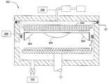
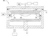
도 2a는 본 발명의 다른 실시예에 따른 처리 장치(200)의 개략적인 횡단면도이다. 도 2a에 도시한 바와 같이, 스커트(204)는 샤워헤드(202)로부터 이격될 수 있다. 스커트(204)가 샤워헤드(202)로부터 이격되었기 때문에, 샤워헤드(202)는 제 1 파워 소오스(206)에 연결될 수 있으며 상기 스커트(204)는 제 2 파워 소오스(208)에 연결될 수 있다. 일 실시예에서, 동일한 파워 소오스가 스커트(204) 및 샤워헤드(202) 모드에 별도로 연결될 수 있다. 일 실시예에서, 파워 소오스(206,208)는 샤워헤드(202) 및 스커트(204) 각각에 RF 전류를 분배하는 RF 파워 소오스를 포함한다.2A is a schematic cross-sectional view of a
상기 스커트(204)는 샤워헤드(202)로부터 이격되었기 때문에 보조 전극으로서의 기능을 한다. 스커트(204)는 샤워헤드(202)가 바이어스되는대로 전기적으로 바이어스된다. 일 실시예에서, 스커트(204)는 샤워헤드(202)와 동일한 전위에서 전기적으로 바이어스된다. 다른 실시예에서, 샤워헤드(202) 및 스커트(204)는 다른 전기 전위에서 전기적으로 바이어스될 수 있다.The
스커트(204)는 화살표 "C"로 나타낸 거리만큼 서셉터로부터 이격될 수 있다. 처리 중에, 스커트(204)는 도 2b에 화살표 "D"로 나타낸 거리만큼 서셉터로부터 이격될 수 있다. 스커트(204)는 챔버 몸체 내에 추가의 전극 표면을 제공한다. 애노드로서 접지되는 서셉터 및 챔버 벽은 표면적을 가진다. 샤워헤드(202)로부터 아래로 연장함으로써 스커트(204)는 처리 중에 플라즈마가 보이는 벽의 하나 또는 그보다 많은 부분들을 차단함으로써, 플라즈마가 처리 공정 중에 보이거나 노출되는 애노드의 표면적을 감소시킨다. 그러므로, 전기적으로 바이어스된 스커트(204)는 애노드 표면적을 감소시키고 접지로 이용가능한 통로를 감소시킴으로써 접지된 서셉터와 상호작용한다. 스커트(204)의 존재와 스커트(204)의 형상 및 서셉터와의 작용은 플라즈마에 영향을 끼침으로써 기판 상의 증착에도 영향을 끼친다. 접지된 애노드는 플라즈마를 애노드에 더 가깝게 당김으로써 기판의 중앙으로부터 더 멀어지게 된다. 전기적으로 바이어스된 스커트(204)는 플라즈마가 보이는 애노드 표면적을 감소시키며 적은 양의 플라즈마를 중앙으로부터 멀어지게 당기는 경향이 있다. 그러므로, 스커트(204)의 형상 및 위치는 장치(200) 내에서의 플라즈마의 균일한 분포를 허용함으로써 기판 상에 증착된 재료의 균일한 특성을 허용할 수 있게 플라즈마를 형상화하도록 조절될 수 있다.The
도 3은 본 발명의 일 실시예에 따른 가스 분배 샤워헤드(302) 및 스커트(304)의 개략적인 등각도이다. 샤워헤드(302)는 샤워헤드를 관통하는 복수의 가스 통로(306)를 가진다. 도 3에 도시한 바와 같이, 스커트(304)는 샤워헤드(302)의 주변부를 따라 배열될 수 있다. 스커트(304)는 샤워헤드(302)의 주변부로부터 연장할 수 있다. 일 실시예에서, 스커트(304)는 샤워헤드(302)의 주변부 주위에서 단속적일 수 있다.3 is a schematic isometric view of
도 4는 본 발명의 다른 실시예에 따른 가스 분배 샤워헤드(402) 및 스커트(404)의 개략적인 등각도이다. 도 4에 도시한 바와 같이, 스커트(404)는 샤워헤드(402) 주위에서 실질적으로 연속적인 구조를 가질 수 있다. 일 실시예에서, 스커트(404)는 샤워헤드(404)의 전체 주변부에 대해 동일한 거리만큼 샤워헤드(402)로부터 아래로 연장한다. 다른 실시예에서, 스커트(404)는 샤워헤드(402)의 전체 주변부에 대해 가변 거리만큼 샤워헤드(402)로부터 연장한다.4 is a schematic isometric view of
스커트의 형상은 가변될 수 있으며 본 발명에서 도시된 형상에 한정된 것이라고 이해해서는 안 된다. 스커트의 형상 및 샤워헤드 아래로 연장하는 거리는 처리 챔버 내의 소정의 플라즈마 분포를 달성하고 그에 따라 소정의 필름 특성을 달성하도록 가변될 수 있다.The shape of the skirt can vary and should not be understood to be limited to the shape shown in the present invention. The shape of the skirt and the distance extending below the showerhead can be varied to achieve the desired plasma distribution in the processing chamber and thus to achieve the desired film properties.
처리 챔버 내에 전기적으로 바이어스된 스커트를 포함함으로써, 전극 표면적이 접지 표면적보다 증가된다. 따라서, 플라즈마는 처리 챔버 전체에 걸쳐 균일하게 확산되며 필름 두께 및 특성들이 실질적으로 균일해질 수 있다.By including an electrically biased skirt in the processing chamber, the electrode surface area is increased above the ground surface area. Thus, the plasma can be uniformly spread throughout the processing chamber and the film thickness and properties can be substantially uniform.
본 발명의 실시예들에 대해 설명하였지만, 본 발명의 기본 범주로부터 이탈함이 없는 본 발명의 다른 그리고 추가의 실시예들이 창안될 수 있으며 본 발명의 범주는 다음의 특허청구범위에 의해 결정된다.While embodiments of the invention have been described, other and further embodiments of the invention can be devised without departing from the basic scope thereof, and the scope thereof is determined by the claims that follow.
Claims (15)
Translated fromKorean상기 처리 챔버 몸체 내에 배열되는 가스 분배 샤워헤드로서, 상기 샤워헤드가 제 1 파워 소오스에 연결되며 일반적으로 직사각형 형상을 가지는, 가스 분배 샤워헤드와,
상기 처리 챔버 몸체 내측에 배열되며 제 2 파워 소오스 또는 상기 제 1 파워 소오스에 연결되는 보조 전극, 및
상기 처리 챔버 몸체 내에 배열되며 상기 보조 전극 및 가스 분배 샤워헤드로부터 이격된 서셉터를 포함하는,
장치.
The processing chamber body,
A gas distribution showerhead arranged in the processing chamber body, the showerhead being connected to a first power source and having a generally rectangular shape;
An auxiliary electrode arranged inside the processing chamber body and connected to a second power source or the first power source, and
A susceptor arranged in the processing chamber body and spaced apart from the auxiliary electrode and a gas distribution showerhead,
Device.
상기 가스 분배 샤워헤드 및 보조 전극은 하나의 일체형 부품 재료를 포함하는,
장치.
The method of claim 1,
Wherein the gas distribution showerhead and the auxiliary electrode comprise one integral part material,
Device.
상기 가스 분배 샤워헤드는 실질적으로 직사각형 형상을 가지며, 상기 보조 전극은 상기 가스 분배 샤워헤드의 코너에서 상기 가스 분배 샤워헤드에 연결되며, 상기 보조 전극은 상기 가스 분배 샤워헤드의 에지를 따라 상기 가스 분배 샤워헤드에 연결되는,
장치.
The method of claim 1,
The gas distribution showerhead has a substantially rectangular shape, the auxiliary electrode is connected to the gas distribution showerhead at a corner of the gas distribution showerhead, and the auxiliary electrode distributes the gas along an edge of the gas distribution showerhead. Connected to the showerhead,
Device.
상기 보조 전극은 상기 제 1 파워 소오스에 연결되는,
장치.
The method of claim 1,
The auxiliary electrode is connected to the first power source,
Device.
상기 가스 분배 샤워헤드 및 보조 전극은 함께 연결되는,
장치.
The method of claim 1,
The gas distribution showerhead and the auxiliary electrode are connected together,
Device.
상기 가스 분배 샤워헤드 및 보조 전극은 서로 전기 절연되는,
장치.
The method of claim 1,
The gas distribution showerhead and the auxiliary electrode are electrically insulated from each other,
Device.
가스 분배 샤워헤드 몸체로서, 상류 측과 하류 측을 가지며 상기 상류 측과 하류 측 사이로 연장하는 하나 또는 그보다 많은 가스 통로를 가지며 일반적으로 직사각형 형상을 가지는, 가스 분배 샤워헤드 몸체, 및
상기 가스 분배 샤워헤드 몸체에 연결되고 상기 하류 측에서 상기 가스 분배 샤워헤드 몸체로부터 연장하는 하나 또는 그보다 많은 보조 전극을 포함하는,
가스 분배 샤워헤드.
As a gas distribution showerhead,
A gas distribution showerhead body, the gas distribution showerhead body having an upstream side and a downstream side and having one or more gas passages extending between the upstream side and the downstream side and generally having a rectangular shape, and
One or more auxiliary electrodes connected to the gas distribution showerhead body and extending from the gas distribution showerhead body on the downstream side,
Gas distribution showerhead.
하나 또는 그보다 많은 상기 보조 전극은 상기 가스 분배 샤워헤드 몸체의 주변부에 연결되고 상기 가스 분배 샤워헤드 몸체의 하나 또는 그보다 많은 코너에 연결되는,
가스 분배 샤워헤드.
The method of claim 7, wherein
One or more said auxiliary electrodes are connected to a periphery of said gas distribution showerhead body and to one or more corners of said gas distribution showerhead body,
Gas distribution showerhead.
상기 가스 분배 샤워헤드 몸체 및 하나 또는 그보다 많은 보조 전극은 하나의 일체형 부품 재료를 포함하는,
가스 분배 샤워헤드.
The method of claim 7, wherein
Wherein the gas distribution showerhead body and one or more auxiliary electrodes comprise one integral part material,
Gas distribution showerhead.
상기 가스 분배 샤워헤드 몸체 및 하나 또는 그보다 많은 보조 전극은 함께 연결되는 별도 부품이며 하나 또는 그보다 많은 상기 보조 전극은 함께 연결되는 복수의 부품을 포함하는,
가스 분배 샤워헤드.
The method of claim 7, wherein
Wherein said gas distribution showerhead body and one or more auxiliary electrodes are separate parts connected together and one or more said auxiliary electrodes comprise a plurality of parts connected together,
Gas distribution showerhead.
처리 챔버 몸체와,
상기 처리 챔버 몸체 내에 배열되는 서셉터와,
상기 처리 챔버 몸체 내에 배열되고 상기 서셉터로부터 분리되며, 상기 서셉터를 지향하는 하류 표면 및 상기 하류 표면과 반대편의 상류 표면을 가지며 일반적으로 직사각형 형상을 가지는 가스 분배 샤워헤드, 및
상기 처리 챔버 몸체 내의 상기 가스 분배 샤워헤드와 상기 서셉터 사이에 배열되며, 파워 소오스에 연결되고 상기 서셉터와 상기 가스 분배 샤워헤드 사이의 처리 공간을 적어도 부분적으로 에워싸는 하나 또는 그보다 많은 보조 전극을 포함하는,
플라즈마 강화 화학 기상 증착 장치.
A plasma enhanced chemical vapor deposition apparatus,
The processing chamber body,
A susceptor arranged in the processing chamber body,
A gas distribution showerhead arranged in the processing chamber body and separated from the susceptor, the gas distribution showerhead having a downstream surface facing the susceptor and an upstream surface opposite the downstream surface and generally having a rectangular shape, and
One or more auxiliary electrodes arranged between the gas distribution showerhead and the susceptor in the processing chamber body, the one or more auxiliary electrodes connected to a power source and at least partially surrounding a processing space between the susceptor and the gas distribution showerhead doing,
Plasma enhanced chemical vapor deposition apparatus.
하나 또는 그보다 많은 상기 보조 전극은 상기 가스 분배 샤워헤드에 연결되며, 하나 또는 그보다 많은 상기 보조 전극과 상기 가스 분배 샤워헤드는 동일한 상기 파워 소오스에 연결되며, 상기 가스 분배 샤워헤드는 실질적으로 직사각형 형상을 가지며 하나 또는 그보다 많은 상기 보조 전극은 상기 가스 분배 샤워헤드의 코너에 연결되며 복수의 부품을 포함하는,
플라즈마 강화 화학 기상 증착 장치.
The method of claim 11,
One or more of the auxiliary electrodes is connected to the gas distribution showerhead, one or more of the auxiliary electrodes and the gas distribution showerhead are connected to the same power source, and the gas distribution showerhead has a substantially rectangular shape. One or more of said auxiliary electrodes connected to a corner of said gas distribution showerhead and comprising a plurality of components,
Plasma enhanced chemical vapor deposition apparatus.
하나 또는 그보다 많은 상기 보조 전극은 상기 가스 분배 샤워헤드와 상기 서셉터로부터 전기 절연되는,
플라즈마 강화 화학 기상 증착 장치.
The method of claim 11,
One or more said auxiliary electrodes are electrically insulated from said gas distribution showerhead and said susceptor,
Plasma enhanced chemical vapor deposition apparatus.
하나 또는 그보다 많은 상기 보조 전극은 상기 가스 분배 샤워헤드의 주변부에 연결되고 상기 하류 표면으로부터 연장하는,
플라즈마 강화 화학 기상 증착 장치.
The method of claim 11,
One or more said auxiliary electrodes are connected to a periphery of said gas distribution showerhead and extend from said downstream surface,
Plasma enhanced chemical vapor deposition apparatus.
하나 또는 그보다 많은 상기 보조 전극과 상기 샤워헤드는 하나의 일체형 부품 재료를 포함하는,
플라즈마 강화 화학 기상 증착 장치.
The method of claim 11,
One or more said auxiliary electrode and said showerhead comprise one integral part material,
Plasma enhanced chemical vapor deposition apparatus.
Applications Claiming Priority (2)
| Application Number | Priority Date | Filing Date | Title |
|---|---|---|---|
| US7451508P | 2008-06-20 | 2008-06-20 | |
| US61/074,515 | 2008-06-20 |
Publications (1)
| Publication Number | Publication Date |
|---|---|
| KR20110031466Atrue KR20110031466A (en) | 2011-03-28 |
Family
ID=41434621
Family Applications (1)
| Application Number | Title | Priority Date | Filing Date |
|---|---|---|---|
| KR1020117001095AWithdrawnKR20110031466A (en) | 2008-06-20 | 2009-05-07 | Gas Distribution Showerhead Skirt |
Country Status (4)
| Country | Link |
|---|---|
| KR (1) | KR20110031466A (en) |
| CN (1) | CN102047388A (en) |
| TW (1) | TW201012963A (en) |
| WO (1) | WO2009154889A2 (en) |
Cited By (3)
| Publication number | Priority date | Publication date | Assignee | Title |
|---|---|---|---|---|
| KR101280240B1 (en)* | 2011-10-07 | 2013-07-05 | 주식회사 테스 | Substrate processing apparatus |
| US11488804B2 (en) | 2019-05-14 | 2022-11-01 | Samsung Electronics Co., Ltd. | Shower head assembly and plasma processing apparatus having the same |
| KR20240158520A (en)* | 2023-04-27 | 2024-11-05 | (주)티티에스 | Air flow improvement device of the showerhead corner area |
Families Citing this family (370)
| Publication number | Priority date | Publication date | Assignee | Title |
|---|---|---|---|---|
| US10378106B2 (en) | 2008-11-14 | 2019-08-13 | Asm Ip Holding B.V. | Method of forming insulation film by modified PEALD |
| US9394608B2 (en) | 2009-04-06 | 2016-07-19 | Asm America, Inc. | Semiconductor processing reactor and components thereof |
| US8802201B2 (en) | 2009-08-14 | 2014-08-12 | Asm America, Inc. | Systems and methods for thin-film deposition of metal oxides using excited nitrogen-oxygen species |
| JP5445252B2 (en)* | 2010-03-16 | 2014-03-19 | 東京エレクトロン株式会社 | Deposition equipment |
| US9312155B2 (en) | 2011-06-06 | 2016-04-12 | Asm Japan K.K. | High-throughput semiconductor-processing apparatus equipped with multiple dual-chamber modules |
| US10364496B2 (en) | 2011-06-27 | 2019-07-30 | Asm Ip Holding B.V. | Dual section module having shared and unshared mass flow controllers |
| US10854498B2 (en) | 2011-07-15 | 2020-12-01 | Asm Ip Holding B.V. | Wafer-supporting device and method for producing same |
| US20130023129A1 (en) | 2011-07-20 | 2013-01-24 | Asm America, Inc. | Pressure transmitter for a semiconductor processing environment |
| US9017481B1 (en) | 2011-10-28 | 2015-04-28 | Asm America, Inc. | Process feed management for semiconductor substrate processing |
| US9558931B2 (en) | 2012-07-27 | 2017-01-31 | Asm Ip Holding B.V. | System and method for gas-phase sulfur passivation of a semiconductor surface |
| US9659799B2 (en) | 2012-08-28 | 2017-05-23 | Asm Ip Holding B.V. | Systems and methods for dynamic semiconductor process scheduling |
| US9021985B2 (en) | 2012-09-12 | 2015-05-05 | Asm Ip Holdings B.V. | Process gas management for an inductively-coupled plasma deposition reactor |
| US10714315B2 (en) | 2012-10-12 | 2020-07-14 | Asm Ip Holdings B.V. | Semiconductor reaction chamber showerhead |
| CN103874314B (en)* | 2012-12-17 | 2016-10-05 | 中微半导体设备(上海)有限公司 | A kind of inductively coupled plasma device |
| US20160376700A1 (en) | 2013-02-01 | 2016-12-29 | Asm Ip Holding B.V. | System for treatment of deposition reactor |
| US9484191B2 (en) | 2013-03-08 | 2016-11-01 | Asm Ip Holding B.V. | Pulsed remote plasma method and system |
| US9589770B2 (en) | 2013-03-08 | 2017-03-07 | Asm Ip Holding B.V. | Method and systems for in-situ formation of intermediate reactive species |
| US8993054B2 (en) | 2013-07-12 | 2015-03-31 | Asm Ip Holding B.V. | Method and system to reduce outgassing in a reaction chamber |
| CN103397308A (en)* | 2013-08-01 | 2013-11-20 | 光垒光电科技(上海)有限公司 | Spray head used for MOCVD equipment |
| CN103436856A (en)* | 2013-08-01 | 2013-12-11 | 光垒光电科技(上海)有限公司 | Reaction cavity |
| US9793115B2 (en) | 2013-08-14 | 2017-10-17 | Asm Ip Holding B.V. | Structures and devices including germanium-tin films and methods of forming same |
| US9240412B2 (en) | 2013-09-27 | 2016-01-19 | Asm Ip Holding B.V. | Semiconductor structure and device and methods of forming same using selective epitaxial process |
| US9605343B2 (en) | 2013-11-13 | 2017-03-28 | Asm Ip Holding B.V. | Method for forming conformal carbon films, structures conformal carbon film, and system of forming same |
| US10683571B2 (en) | 2014-02-25 | 2020-06-16 | Asm Ip Holding B.V. | Gas supply manifold and method of supplying gases to chamber using same |
| US10167557B2 (en) | 2014-03-18 | 2019-01-01 | Asm Ip Holding B.V. | Gas distribution system, reactor including the system, and methods of using the same |
| US11015245B2 (en) | 2014-03-19 | 2021-05-25 | Asm Ip Holding B.V. | Gas-phase reactor and system having exhaust plenum and components thereof |
| US10858737B2 (en) | 2014-07-28 | 2020-12-08 | Asm Ip Holding B.V. | Showerhead assembly and components thereof |
| US9890456B2 (en) | 2014-08-21 | 2018-02-13 | Asm Ip Holding B.V. | Method and system for in situ formation of gas-phase compounds |
| US9657845B2 (en) | 2014-10-07 | 2017-05-23 | Asm Ip Holding B.V. | Variable conductance gas distribution apparatus and method |
| US10941490B2 (en) | 2014-10-07 | 2021-03-09 | Asm Ip Holding B.V. | Multiple temperature range susceptor, assembly, reactor and system including the susceptor, and methods of using the same |
| KR102300403B1 (en) | 2014-11-19 | 2021-09-09 | 에이에스엠 아이피 홀딩 비.브이. | Method of depositing thin film |
| KR102263121B1 (en) | 2014-12-22 | 2021-06-09 | 에이에스엠 아이피 홀딩 비.브이. | Semiconductor device and manufacuring method thereof |
| US10529542B2 (en) | 2015-03-11 | 2020-01-07 | Asm Ip Holdings B.V. | Cross-flow reactor and method |
| US10276355B2 (en) | 2015-03-12 | 2019-04-30 | Asm Ip Holding B.V. | Multi-zone reactor, system including the reactor, and method of using the same |
| US10458018B2 (en) | 2015-06-26 | 2019-10-29 | Asm Ip Holding B.V. | Structures including metal carbide material, devices including the structures, and methods of forming same |
| US10600673B2 (en) | 2015-07-07 | 2020-03-24 | Asm Ip Holding B.V. | Magnetic susceptor to baseplate seal |
| US10043661B2 (en) | 2015-07-13 | 2018-08-07 | Asm Ip Holding B.V. | Method for protecting layer by forming hydrocarbon-based extremely thin film |
| US10083836B2 (en) | 2015-07-24 | 2018-09-25 | Asm Ip Holding B.V. | Formation of boron-doped titanium metal films with high work function |
| US10087525B2 (en) | 2015-08-04 | 2018-10-02 | Asm Ip Holding B.V. | Variable gap hard stop design |
| US9647114B2 (en) | 2015-08-14 | 2017-05-09 | Asm Ip Holding B.V. | Methods of forming highly p-type doped germanium tin films and structures and devices including the films |
| US9960072B2 (en) | 2015-09-29 | 2018-05-01 | Asm Ip Holding B.V. | Variable adjustment for precise matching of multiple chamber cavity housings |
| US10211308B2 (en) | 2015-10-21 | 2019-02-19 | Asm Ip Holding B.V. | NbMC layers |
| US10322384B2 (en) | 2015-11-09 | 2019-06-18 | Asm Ip Holding B.V. | Counter flow mixer for process chamber |
| US11139308B2 (en) | 2015-12-29 | 2021-10-05 | Asm Ip Holding B.V. | Atomic layer deposition of III-V compounds to form V-NAND devices |
| US10468251B2 (en) | 2016-02-19 | 2019-11-05 | Asm Ip Holding B.V. | Method for forming spacers using silicon nitride film for spacer-defined multiple patterning |
| US10529554B2 (en) | 2016-02-19 | 2020-01-07 | Asm Ip Holding B.V. | Method for forming silicon nitride film selectively on sidewalls or flat surfaces of trenches |
| US10501866B2 (en) | 2016-03-09 | 2019-12-10 | Asm Ip Holding B.V. | Gas distribution apparatus for improved film uniformity in an epitaxial system |
| US10343920B2 (en) | 2016-03-18 | 2019-07-09 | Asm Ip Holding B.V. | Aligned carbon nanotubes |
| US9892913B2 (en) | 2016-03-24 | 2018-02-13 | Asm Ip Holding B.V. | Radial and thickness control via biased multi-port injection settings |
| US10190213B2 (en) | 2016-04-21 | 2019-01-29 | Asm Ip Holding B.V. | Deposition of metal borides |
| US10865475B2 (en) | 2016-04-21 | 2020-12-15 | Asm Ip Holding B.V. | Deposition of metal borides and silicides |
| US10087522B2 (en) | 2016-04-21 | 2018-10-02 | Asm Ip Holding B.V. | Deposition of metal borides |
| US10032628B2 (en) | 2016-05-02 | 2018-07-24 | Asm Ip Holding B.V. | Source/drain performance through conformal solid state doping |
| US10367080B2 (en) | 2016-05-02 | 2019-07-30 | Asm Ip Holding B.V. | Method of forming a germanium oxynitride film |
| KR102592471B1 (en) | 2016-05-17 | 2023-10-20 | 에이에스엠 아이피 홀딩 비.브이. | Method of forming metal interconnection and method of fabricating semiconductor device using the same |
| US10388509B2 (en) | 2016-06-28 | 2019-08-20 | Asm Ip Holding B.V. | Formation of epitaxial layers via dislocation filtering |
| US9859151B1 (en) | 2016-07-08 | 2018-01-02 | Asm Ip Holding B.V. | Selective film deposition method to form air gaps |
| US10612137B2 (en) | 2016-07-08 | 2020-04-07 | Asm Ip Holdings B.V. | Organic reactants for atomic layer deposition |
| US9793135B1 (en) | 2016-07-14 | 2017-10-17 | ASM IP Holding B.V | Method of cyclic dry etching using etchant film |
| US10714385B2 (en) | 2016-07-19 | 2020-07-14 | Asm Ip Holding B.V. | Selective deposition of tungsten |
| KR102354490B1 (en) | 2016-07-27 | 2022-01-21 | 에이에스엠 아이피 홀딩 비.브이. | Method of processing a substrate |
| US9812320B1 (en) | 2016-07-28 | 2017-11-07 | Asm Ip Holding B.V. | Method and apparatus for filling a gap |
| US10177025B2 (en) | 2016-07-28 | 2019-01-08 | Asm Ip Holding B.V. | Method and apparatus for filling a gap |
| US9887082B1 (en) | 2016-07-28 | 2018-02-06 | Asm Ip Holding B.V. | Method and apparatus for filling a gap |
| KR102532607B1 (en) | 2016-07-28 | 2023-05-15 | 에이에스엠 아이피 홀딩 비.브이. | Substrate processing apparatus and method of operating the same |
| US10395919B2 (en) | 2016-07-28 | 2019-08-27 | Asm Ip Holding B.V. | Method and apparatus for filling a gap |
| US10090316B2 (en) | 2016-09-01 | 2018-10-02 | Asm Ip Holding B.V. | 3D stacked multilayer semiconductor memory using doped select transistor channel |
| US10410943B2 (en) | 2016-10-13 | 2019-09-10 | Asm Ip Holding B.V. | Method for passivating a surface of a semiconductor and related systems |
| US10643826B2 (en) | 2016-10-26 | 2020-05-05 | Asm Ip Holdings B.V. | Methods for thermally calibrating reaction chambers |
| US11532757B2 (en) | 2016-10-27 | 2022-12-20 | Asm Ip Holding B.V. | Deposition of charge trapping layers |
| US10714350B2 (en) | 2016-11-01 | 2020-07-14 | ASM IP Holdings, B.V. | Methods for forming a transition metal niobium nitride film on a substrate by atomic layer deposition and related semiconductor device structures |
| US10643904B2 (en) | 2016-11-01 | 2020-05-05 | Asm Ip Holdings B.V. | Methods for forming a semiconductor device and related semiconductor device structures |
| US10229833B2 (en) | 2016-11-01 | 2019-03-12 | Asm Ip Holding B.V. | Methods for forming a transition metal nitride film on a substrate by atomic layer deposition and related semiconductor device structures |
| US10435790B2 (en) | 2016-11-01 | 2019-10-08 | Asm Ip Holding B.V. | Method of subatmospheric plasma-enhanced ALD using capacitively coupled electrodes with narrow gap |
| US10134757B2 (en) | 2016-11-07 | 2018-11-20 | Asm Ip Holding B.V. | Method of processing a substrate and a device manufactured by using the method |
| US10403476B2 (en) | 2016-11-09 | 2019-09-03 | Lam Research Corporation | Active showerhead |
| KR102546317B1 (en) | 2016-11-15 | 2023-06-21 | 에이에스엠 아이피 홀딩 비.브이. | Gas supply unit and substrate processing apparatus including the same |
| US10340135B2 (en) | 2016-11-28 | 2019-07-02 | Asm Ip Holding B.V. | Method of topologically restricted plasma-enhanced cyclic deposition of silicon or metal nitride |
| KR102762543B1 (en) | 2016-12-14 | 2025-02-05 | 에이에스엠 아이피 홀딩 비.브이. | Substrate processing apparatus |
| US11581186B2 (en) | 2016-12-15 | 2023-02-14 | Asm Ip Holding B.V. | Sequential infiltration synthesis apparatus |
| US9916980B1 (en) | 2016-12-15 | 2018-03-13 | Asm Ip Holding B.V. | Method of forming a structure on a substrate |
| US11447861B2 (en) | 2016-12-15 | 2022-09-20 | Asm Ip Holding B.V. | Sequential infiltration synthesis apparatus and a method of forming a patterned structure |
| KR102700194B1 (en) | 2016-12-19 | 2024-08-28 | 에이에스엠 아이피 홀딩 비.브이. | Substrate processing apparatus |
| US10269558B2 (en) | 2016-12-22 | 2019-04-23 | Asm Ip Holding B.V. | Method of forming a structure on a substrate |
| US10867788B2 (en) | 2016-12-28 | 2020-12-15 | Asm Ip Holding B.V. | Method of forming a structure on a substrate |
| US11390950B2 (en) | 2017-01-10 | 2022-07-19 | Asm Ip Holding B.V. | Reactor system and method to reduce residue buildup during a film deposition process |
| US10655221B2 (en) | 2017-02-09 | 2020-05-19 | Asm Ip Holding B.V. | Method for depositing oxide film by thermal ALD and PEALD |
| US10468261B2 (en) | 2017-02-15 | 2019-11-05 | Asm Ip Holding B.V. | Methods for forming a metallic film on a substrate by cyclical deposition and related semiconductor device structures |
| US10529563B2 (en) | 2017-03-29 | 2020-01-07 | Asm Ip Holdings B.V. | Method for forming doped metal oxide films on a substrate by cyclical deposition and related semiconductor device structures |
| US10283353B2 (en) | 2017-03-29 | 2019-05-07 | Asm Ip Holding B.V. | Method of reforming insulating film deposited on substrate with recess pattern |
| US10103040B1 (en) | 2017-03-31 | 2018-10-16 | Asm Ip Holding B.V. | Apparatus and method for manufacturing a semiconductor device |
| USD830981S1 (en) | 2017-04-07 | 2018-10-16 | Asm Ip Holding B.V. | Susceptor for semiconductor substrate processing apparatus |
| KR102457289B1 (en) | 2017-04-25 | 2022-10-21 | 에이에스엠 아이피 홀딩 비.브이. | Method for depositing a thin film and manufacturing a semiconductor device |
| US10892156B2 (en) | 2017-05-08 | 2021-01-12 | Asm Ip Holding B.V. | Methods for forming a silicon nitride film on a substrate and related semiconductor device structures |
| US10770286B2 (en) | 2017-05-08 | 2020-09-08 | Asm Ip Holdings B.V. | Methods for selectively forming a silicon nitride film on a substrate and related semiconductor device structures |
| US10446393B2 (en) | 2017-05-08 | 2019-10-15 | Asm Ip Holding B.V. | Methods for forming silicon-containing epitaxial layers and related semiconductor device structures |
| US10504742B2 (en) | 2017-05-31 | 2019-12-10 | Asm Ip Holding B.V. | Method of atomic layer etching using hydrogen plasma |
| US10886123B2 (en) | 2017-06-02 | 2021-01-05 | Asm Ip Holding B.V. | Methods for forming low temperature semiconductor layers and related semiconductor device structures |
| US12040200B2 (en) | 2017-06-20 | 2024-07-16 | Asm Ip Holding B.V. | Semiconductor processing apparatus and methods for calibrating a semiconductor processing apparatus |
| US11306395B2 (en) | 2017-06-28 | 2022-04-19 | Asm Ip Holding B.V. | Methods for depositing a transition metal nitride film on a substrate by atomic layer deposition and related deposition apparatus |
| US10685834B2 (en) | 2017-07-05 | 2020-06-16 | Asm Ip Holdings B.V. | Methods for forming a silicon germanium tin layer and related semiconductor device structures |
| KR20190009245A (en) | 2017-07-18 | 2019-01-28 | 에이에스엠 아이피 홀딩 비.브이. | Methods for forming a semiconductor device structure and related semiconductor device structures |
| US10541333B2 (en) | 2017-07-19 | 2020-01-21 | Asm Ip Holding B.V. | Method for depositing a group IV semiconductor and related semiconductor device structures |
| US11018002B2 (en) | 2017-07-19 | 2021-05-25 | Asm Ip Holding B.V. | Method for selectively depositing a Group IV semiconductor and related semiconductor device structures |
| US11374112B2 (en) | 2017-07-19 | 2022-06-28 | Asm Ip Holding B.V. | Method for depositing a group IV semiconductor and related semiconductor device structures |
| US10312055B2 (en) | 2017-07-26 | 2019-06-04 | Asm Ip Holding B.V. | Method of depositing film by PEALD using negative bias |
| US10590535B2 (en) | 2017-07-26 | 2020-03-17 | Asm Ip Holdings B.V. | Chemical treatment, deposition and/or infiltration apparatus and method for using the same |
| US10605530B2 (en) | 2017-07-26 | 2020-03-31 | Asm Ip Holding B.V. | Assembly of a liner and a flange for a vertical furnace as well as the liner and the vertical furnace |
| TWI815813B (en) | 2017-08-04 | 2023-09-21 | 荷蘭商Asm智慧財產控股公司 | Showerhead assembly for distributing a gas within a reaction chamber |
| US10692741B2 (en) | 2017-08-08 | 2020-06-23 | Asm Ip Holdings B.V. | Radiation shield |
| US10770336B2 (en) | 2017-08-08 | 2020-09-08 | Asm Ip Holding B.V. | Substrate lift mechanism and reactor including same |
| US11139191B2 (en) | 2017-08-09 | 2021-10-05 | Asm Ip Holding B.V. | Storage apparatus for storing cassettes for substrates and processing apparatus equipped therewith |
| US11769682B2 (en) | 2017-08-09 | 2023-09-26 | Asm Ip Holding B.V. | Storage apparatus for storing cassettes for substrates and processing apparatus equipped therewith |
| US10249524B2 (en) | 2017-08-09 | 2019-04-02 | Asm Ip Holding B.V. | Cassette holder assembly for a substrate cassette and holding member for use in such assembly |
| US10236177B1 (en) | 2017-08-22 | 2019-03-19 | ASM IP Holding B.V.. | Methods for depositing a doped germanium tin semiconductor and related semiconductor device structures |
| USD900036S1 (en) | 2017-08-24 | 2020-10-27 | Asm Ip Holding B.V. | Heater electrical connector and adapter |
| US11830730B2 (en) | 2017-08-29 | 2023-11-28 | Asm Ip Holding B.V. | Layer forming method and apparatus |
| US11056344B2 (en) | 2017-08-30 | 2021-07-06 | Asm Ip Holding B.V. | Layer forming method |
| US11295980B2 (en) | 2017-08-30 | 2022-04-05 | Asm Ip Holding B.V. | Methods for depositing a molybdenum metal film over a dielectric surface of a substrate by a cyclical deposition process and related semiconductor device structures |
| KR102491945B1 (en) | 2017-08-30 | 2023-01-26 | 에이에스엠 아이피 홀딩 비.브이. | Substrate processing apparatus |
| KR102401446B1 (en) | 2017-08-31 | 2022-05-24 | 에이에스엠 아이피 홀딩 비.브이. | Substrate processing apparatus |
| US10607895B2 (en) | 2017-09-18 | 2020-03-31 | Asm Ip Holdings B.V. | Method for forming a semiconductor device structure comprising a gate fill metal |
| KR102630301B1 (en) | 2017-09-21 | 2024-01-29 | 에이에스엠 아이피 홀딩 비.브이. | Method of sequential infiltration synthesis treatment of infiltrateable material and structures and devices formed using same |
| US10844484B2 (en) | 2017-09-22 | 2020-11-24 | Asm Ip Holding B.V. | Apparatus for dispensing a vapor phase reactant to a reaction chamber and related methods |
| US10658205B2 (en) | 2017-09-28 | 2020-05-19 | Asm Ip Holdings B.V. | Chemical dispensing apparatus and methods for dispensing a chemical to a reaction chamber |
| US10403504B2 (en) | 2017-10-05 | 2019-09-03 | Asm Ip Holding B.V. | Method for selectively depositing a metallic film on a substrate |
| US10319588B2 (en) | 2017-10-10 | 2019-06-11 | Asm Ip Holding B.V. | Method for depositing a metal chalcogenide on a substrate by cyclical deposition |
| US10923344B2 (en) | 2017-10-30 | 2021-02-16 | Asm Ip Holding B.V. | Methods for forming a semiconductor structure and related semiconductor structures |
| KR102443047B1 (en) | 2017-11-16 | 2022-09-14 | 에이에스엠 아이피 홀딩 비.브이. | Method of processing a substrate and a device manufactured by the same |
| US10910262B2 (en) | 2017-11-16 | 2021-02-02 | Asm Ip Holding B.V. | Method of selectively depositing a capping layer structure on a semiconductor device structure |
| US11022879B2 (en) | 2017-11-24 | 2021-06-01 | Asm Ip Holding B.V. | Method of forming an enhanced unexposed photoresist layer |
| CN111344522B (en) | 2017-11-27 | 2022-04-12 | 阿斯莫Ip控股公司 | Including clean mini-environment device |
| WO2019103613A1 (en) | 2017-11-27 | 2019-05-31 | Asm Ip Holding B.V. | A storage device for storing wafer cassettes for use with a batch furnace |
| US10290508B1 (en) | 2017-12-05 | 2019-05-14 | Asm Ip Holding B.V. | Method for forming vertical spacers for spacer-defined patterning |
| US10872771B2 (en) | 2018-01-16 | 2020-12-22 | Asm Ip Holding B. V. | Method for depositing a material film on a substrate within a reaction chamber by a cyclical deposition process and related device structures |
| KR102695659B1 (en) | 2018-01-19 | 2024-08-14 | 에이에스엠 아이피 홀딩 비.브이. | Method for depositing a gap filling layer by plasma assisted deposition |
| TWI799494B (en) | 2018-01-19 | 2023-04-21 | 荷蘭商Asm 智慧財產控股公司 | Deposition method |
| USD903477S1 (en) | 2018-01-24 | 2020-12-01 | Asm Ip Holdings B.V. | Metal clamp |
| US11018047B2 (en) | 2018-01-25 | 2021-05-25 | Asm Ip Holding B.V. | Hybrid lift pin |
| US10535516B2 (en) | 2018-02-01 | 2020-01-14 | Asm Ip Holdings B.V. | Method for depositing a semiconductor structure on a surface of a substrate and related semiconductor structures |
| USD880437S1 (en) | 2018-02-01 | 2020-04-07 | Asm Ip Holding B.V. | Gas supply plate for semiconductor manufacturing apparatus |
| US20190244793A1 (en)* | 2018-02-05 | 2019-08-08 | Lam Research Corporation | Tapered upper electrode for uniformity control in plasma processing |
| US11081345B2 (en) | 2018-02-06 | 2021-08-03 | Asm Ip Holding B.V. | Method of post-deposition treatment for silicon oxide film |
| US10896820B2 (en) | 2018-02-14 | 2021-01-19 | Asm Ip Holding B.V. | Method for depositing a ruthenium-containing film on a substrate by a cyclical deposition process |
| WO2019158960A1 (en) | 2018-02-14 | 2019-08-22 | Asm Ip Holding B.V. | A method for depositing a ruthenium-containing film on a substrate by a cyclical deposition process |
| US10731249B2 (en) | 2018-02-15 | 2020-08-04 | Asm Ip Holding B.V. | Method of forming a transition metal containing film on a substrate by a cyclical deposition process, a method for supplying a transition metal halide compound to a reaction chamber, and related vapor deposition apparatus |
| KR102636427B1 (en) | 2018-02-20 | 2024-02-13 | 에이에스엠 아이피 홀딩 비.브이. | Substrate processing method and apparatus |
| US10658181B2 (en) | 2018-02-20 | 2020-05-19 | Asm Ip Holding B.V. | Method of spacer-defined direct patterning in semiconductor fabrication |
| US10975470B2 (en) | 2018-02-23 | 2021-04-13 | Asm Ip Holding B.V. | Apparatus for detecting or monitoring for a chemical precursor in a high temperature environment |
| US11473195B2 (en) | 2018-03-01 | 2022-10-18 | Asm Ip Holding B.V. | Semiconductor processing apparatus and a method for processing a substrate |
| US11629406B2 (en) | 2018-03-09 | 2023-04-18 | Asm Ip Holding B.V. | Semiconductor processing apparatus comprising one or more pyrometers for measuring a temperature of a substrate during transfer of the substrate |
| US11114283B2 (en) | 2018-03-16 | 2021-09-07 | Asm Ip Holding B.V. | Reactor, system including the reactor, and methods of manufacturing and using same |
| KR102646467B1 (en) | 2018-03-27 | 2024-03-11 | 에이에스엠 아이피 홀딩 비.브이. | Method of forming an electrode on a substrate and a semiconductor device structure including an electrode |
| US11088002B2 (en) | 2018-03-29 | 2021-08-10 | Asm Ip Holding B.V. | Substrate rack and a substrate processing system and method |
| US10510536B2 (en) | 2018-03-29 | 2019-12-17 | Asm Ip Holding B.V. | Method of depositing a co-doped polysilicon film on a surface of a substrate within a reaction chamber |
| US11230766B2 (en) | 2018-03-29 | 2022-01-25 | Asm Ip Holding B.V. | Substrate processing apparatus and method |
| KR102501472B1 (en) | 2018-03-30 | 2023-02-20 | 에이에스엠 아이피 홀딩 비.브이. | Substrate processing method |
| KR102600229B1 (en) | 2018-04-09 | 2023-11-10 | 에이에스엠 아이피 홀딩 비.브이. | Substrate supporting device, substrate processing apparatus including the same and substrate processing method |
| TWI811348B (en) | 2018-05-08 | 2023-08-11 | 荷蘭商Asm 智慧財產控股公司 | Methods for depositing an oxide film on a substrate by a cyclical deposition process and related device structures |
| US12025484B2 (en) | 2018-05-08 | 2024-07-02 | Asm Ip Holding B.V. | Thin film forming method |
| US12272527B2 (en) | 2018-05-09 | 2025-04-08 | Asm Ip Holding B.V. | Apparatus for use with hydrogen radicals and method of using same |
| KR20190129718A (en) | 2018-05-11 | 2019-11-20 | 에이에스엠 아이피 홀딩 비.브이. | Methods for forming a doped metal carbide film on a substrate and related semiconductor device structures |
| KR102596988B1 (en) | 2018-05-28 | 2023-10-31 | 에이에스엠 아이피 홀딩 비.브이. | Method of processing a substrate and a device manufactured by the same |
| US11718913B2 (en) | 2018-06-04 | 2023-08-08 | Asm Ip Holding B.V. | Gas distribution system and reactor system including same |
| TWI840362B (en) | 2018-06-04 | 2024-05-01 | 荷蘭商Asm Ip私人控股有限公司 | Wafer handling chamber with moisture reduction |
| US11286562B2 (en) | 2018-06-08 | 2022-03-29 | Asm Ip Holding B.V. | Gas-phase chemical reactor and method of using same |
| KR102568797B1 (en) | 2018-06-21 | 2023-08-21 | 에이에스엠 아이피 홀딩 비.브이. | Substrate processing system |
| US10797133B2 (en) | 2018-06-21 | 2020-10-06 | Asm Ip Holding B.V. | Method for depositing a phosphorus doped silicon arsenide film and related semiconductor device structures |
| TWI873894B (en) | 2018-06-27 | 2025-02-21 | 荷蘭商Asm Ip私人控股有限公司 | Cyclic deposition methods for forming metal-containing material and films and structures including the metal-containing material |
| KR102854019B1 (en) | 2018-06-27 | 2025-09-02 | 에이에스엠 아이피 홀딩 비.브이. | Periodic deposition method for forming a metal-containing material and films and structures comprising the metal-containing material |
| KR102686758B1 (en) | 2018-06-29 | 2024-07-18 | 에이에스엠 아이피 홀딩 비.브이. | Method for depositing a thin film and manufacturing a semiconductor device |
| US10612136B2 (en) | 2018-06-29 | 2020-04-07 | ASM IP Holding, B.V. | Temperature-controlled flange and reactor system including same |
| US10388513B1 (en) | 2018-07-03 | 2019-08-20 | Asm Ip Holding B.V. | Method for depositing silicon-free carbon-containing film as gap-fill layer by pulse plasma-assisted deposition |
| US10755922B2 (en) | 2018-07-03 | 2020-08-25 | Asm Ip Holding B.V. | Method for depositing silicon-free carbon-containing film as gap-fill layer by pulse plasma-assisted deposition |
| US10767789B2 (en) | 2018-07-16 | 2020-09-08 | Asm Ip Holding B.V. | Diaphragm valves, valve components, and methods for forming valve components |
| US10483099B1 (en) | 2018-07-26 | 2019-11-19 | Asm Ip Holding B.V. | Method for forming thermally stable organosilicon polymer film |
| US11053591B2 (en) | 2018-08-06 | 2021-07-06 | Asm Ip Holding B.V. | Multi-port gas injection system and reactor system including same |
| US10883175B2 (en) | 2018-08-09 | 2021-01-05 | Asm Ip Holding B.V. | Vertical furnace for processing substrates and a liner for use therein |
| US10829852B2 (en) | 2018-08-16 | 2020-11-10 | Asm Ip Holding B.V. | Gas distribution device for a wafer processing apparatus |
| US11430674B2 (en) | 2018-08-22 | 2022-08-30 | Asm Ip Holding B.V. | Sensor array, apparatus for dispensing a vapor phase reactant to a reaction chamber and related methods |
| KR102707956B1 (en) | 2018-09-11 | 2024-09-19 | 에이에스엠 아이피 홀딩 비.브이. | Method for deposition of a thin film |
| US11024523B2 (en) | 2018-09-11 | 2021-06-01 | Asm Ip Holding B.V. | Substrate processing apparatus and method |
| US11049751B2 (en) | 2018-09-14 | 2021-06-29 | Asm Ip Holding B.V. | Cassette supply system to store and handle cassettes and processing apparatus equipped therewith |
| CN110970344B (en) | 2018-10-01 | 2024-10-25 | Asmip控股有限公司 | Substrate holding apparatus, system comprising the same and method of using the same |
| US11232963B2 (en) | 2018-10-03 | 2022-01-25 | Asm Ip Holding B.V. | Substrate processing apparatus and method |
| KR102592699B1 (en) | 2018-10-08 | 2023-10-23 | 에이에스엠 아이피 홀딩 비.브이. | Substrate support unit and apparatuses for depositing thin film and processing the substrate including the same |
| US10847365B2 (en) | 2018-10-11 | 2020-11-24 | Asm Ip Holding B.V. | Method of forming conformal silicon carbide film by cyclic CVD |
| US10811256B2 (en) | 2018-10-16 | 2020-10-20 | Asm Ip Holding B.V. | Method for etching a carbon-containing feature |
| KR102546322B1 (en) | 2018-10-19 | 2023-06-21 | 에이에스엠 아이피 홀딩 비.브이. | Substrate processing apparatus and substrate processing method |
| KR102605121B1 (en) | 2018-10-19 | 2023-11-23 | 에이에스엠 아이피 홀딩 비.브이. | Substrate processing apparatus and substrate processing method |
| USD948463S1 (en) | 2018-10-24 | 2022-04-12 | Asm Ip Holding B.V. | Susceptor for semiconductor substrate supporting apparatus |
| US10381219B1 (en) | 2018-10-25 | 2019-08-13 | Asm Ip Holding B.V. | Methods for forming a silicon nitride film |
| US12378665B2 (en) | 2018-10-26 | 2025-08-05 | Asm Ip Holding B.V. | High temperature coatings for a preclean and etch apparatus and related methods |
| US11087997B2 (en) | 2018-10-31 | 2021-08-10 | Asm Ip Holding B.V. | Substrate processing apparatus for processing substrates |
| KR102748291B1 (en) | 2018-11-02 | 2024-12-31 | 에이에스엠 아이피 홀딩 비.브이. | Substrate support unit and substrate processing apparatus including the same |
| US11572620B2 (en) | 2018-11-06 | 2023-02-07 | Asm Ip Holding B.V. | Methods for selectively depositing an amorphous silicon film on a substrate |
| US11031242B2 (en) | 2018-11-07 | 2021-06-08 | Asm Ip Holding B.V. | Methods for depositing a boron doped silicon germanium film |
| US10847366B2 (en) | 2018-11-16 | 2020-11-24 | Asm Ip Holding B.V. | Methods for depositing a transition metal chalcogenide film on a substrate by a cyclical deposition process |
| US10818758B2 (en) | 2018-11-16 | 2020-10-27 | Asm Ip Holding B.V. | Methods for forming a metal silicate film on a substrate in a reaction chamber and related semiconductor device structures |
| US10559458B1 (en) | 2018-11-26 | 2020-02-11 | Asm Ip Holding B.V. | Method of forming oxynitride film |
| US12040199B2 (en) | 2018-11-28 | 2024-07-16 | Asm Ip Holding B.V. | Substrate processing apparatus for processing substrates |
| US11217444B2 (en) | 2018-11-30 | 2022-01-04 | Asm Ip Holding B.V. | Method for forming an ultraviolet radiation responsive metal oxide-containing film |
| KR102636428B1 (en) | 2018-12-04 | 2024-02-13 | 에이에스엠 아이피 홀딩 비.브이. | A method for cleaning a substrate processing apparatus |
| US11158513B2 (en) | 2018-12-13 | 2021-10-26 | Asm Ip Holding B.V. | Methods for forming a rhenium-containing film on a substrate by a cyclical deposition process and related semiconductor device structures |
| TWI874340B (en) | 2018-12-14 | 2025-03-01 | 荷蘭商Asm Ip私人控股有限公司 | Method of forming device structure, structure formed by the method and system for performing the method |
| TWI866480B (en) | 2019-01-17 | 2024-12-11 | 荷蘭商Asm Ip 私人控股有限公司 | Methods of forming a transition metal containing film on a substrate by a cyclical deposition process |
| KR102727227B1 (en) | 2019-01-22 | 2024-11-07 | 에이에스엠 아이피 홀딩 비.브이. | Semiconductor processing device |
| CN111524788B (en) | 2019-02-01 | 2023-11-24 | Asm Ip私人控股有限公司 | Method for forming topologically selective films of silicon oxide |
| TWI845607B (en) | 2019-02-20 | 2024-06-21 | 荷蘭商Asm Ip私人控股有限公司 | Cyclical deposition method and apparatus for filling a recess formed within a substrate surface |
| TWI838458B (en) | 2019-02-20 | 2024-04-11 | 荷蘭商Asm Ip私人控股有限公司 | Apparatus and methods for plug fill deposition in 3-d nand applications |
| KR102626263B1 (en) | 2019-02-20 | 2024-01-16 | 에이에스엠 아이피 홀딩 비.브이. | Cyclical deposition method including treatment step and apparatus for same |
| TWI873122B (en) | 2019-02-20 | 2025-02-21 | 荷蘭商Asm Ip私人控股有限公司 | Method of filling a recess formed within a surface of a substrate, semiconductor structure formed according to the method, and semiconductor processing apparatus |
| TWI842826B (en) | 2019-02-22 | 2024-05-21 | 荷蘭商Asm Ip私人控股有限公司 | Substrate processing apparatus and method for processing substrate |
| KR102858005B1 (en) | 2019-03-08 | 2025-09-09 | 에이에스엠 아이피 홀딩 비.브이. | Method for Selective Deposition of Silicon Nitride Layer and Structure Including Selectively-Deposited Silicon Nitride Layer |
| KR102782593B1 (en) | 2019-03-08 | 2025-03-14 | 에이에스엠 아이피 홀딩 비.브이. | Structure Including SiOC Layer and Method of Forming Same |
| US11742198B2 (en) | 2019-03-08 | 2023-08-29 | Asm Ip Holding B.V. | Structure including SiOCN layer and method of forming same |
| JP2020167398A (en) | 2019-03-28 | 2020-10-08 | エーエスエム・アイピー・ホールディング・ベー・フェー | Door openers and substrate processing equipment provided with door openers |
| KR102809999B1 (en) | 2019-04-01 | 2025-05-19 | 에이에스엠 아이피 홀딩 비.브이. | Method of manufacturing semiconductor device |
| KR20200123380A (en) | 2019-04-19 | 2020-10-29 | 에이에스엠 아이피 홀딩 비.브이. | Layer forming method and apparatus |
| KR20200125453A (en) | 2019-04-24 | 2020-11-04 | 에이에스엠 아이피 홀딩 비.브이. | Gas-phase reactor system and method of using same |
| US11289326B2 (en) | 2019-05-07 | 2022-03-29 | Asm Ip Holding B.V. | Method for reforming amorphous carbon polymer film |
| KR20200130121A (en) | 2019-05-07 | 2020-11-18 | 에이에스엠 아이피 홀딩 비.브이. | Chemical source vessel with dip tube |
| KR20200130652A (en) | 2019-05-10 | 2020-11-19 | 에이에스엠 아이피 홀딩 비.브이. | Method of depositing material onto a surface and structure formed according to the method |
| JP7612342B2 (en) | 2019-05-16 | 2025-01-14 | エーエスエム・アイピー・ホールディング・ベー・フェー | Wafer boat handling apparatus, vertical batch furnace and method |
| JP7598201B2 (en) | 2019-05-16 | 2024-12-11 | エーエスエム・アイピー・ホールディング・ベー・フェー | Wafer boat handling apparatus, vertical batch furnace and method |
| USD975665S1 (en) | 2019-05-17 | 2023-01-17 | Asm Ip Holding B.V. | Susceptor shaft |
| USD947913S1 (en) | 2019-05-17 | 2022-04-05 | Asm Ip Holding B.V. | Susceptor shaft |
| USD935572S1 (en) | 2019-05-24 | 2021-11-09 | Asm Ip Holding B.V. | Gas channel plate |
| USD922229S1 (en) | 2019-06-05 | 2021-06-15 | Asm Ip Holding B.V. | Device for controlling a temperature of a gas supply unit |
| KR20200141002A (en) | 2019-06-06 | 2020-12-17 | 에이에스엠 아이피 홀딩 비.브이. | Method of using a gas-phase reactor system including analyzing exhausted gas |
| KR20200141931A (en) | 2019-06-10 | 2020-12-21 | 에이에스엠 아이피 홀딩 비.브이. | Method for cleaning quartz epitaxial chambers |
| KR20200143254A (en) | 2019-06-11 | 2020-12-23 | 에이에스엠 아이피 홀딩 비.브이. | Method of forming an electronic structure using an reforming gas, system for performing the method, and structure formed using the method |
| USD944946S1 (en) | 2019-06-14 | 2022-03-01 | Asm Ip Holding B.V. | Shower plate |
| USD931978S1 (en) | 2019-06-27 | 2021-09-28 | Asm Ip Holding B.V. | Showerhead vacuum transport |
| KR20210005515A (en) | 2019-07-03 | 2021-01-14 | 에이에스엠 아이피 홀딩 비.브이. | Temperature control assembly for substrate processing apparatus and method of using same |
| JP7499079B2 (en) | 2019-07-09 | 2024-06-13 | エーエスエム・アイピー・ホールディング・ベー・フェー | Plasma device using coaxial waveguide and substrate processing method |
| CN112216646A (en) | 2019-07-10 | 2021-01-12 | Asm Ip私人控股有限公司 | Substrate supporting assembly and substrate processing device comprising same |
| KR20210010307A (en) | 2019-07-16 | 2021-01-27 | 에이에스엠 아이피 홀딩 비.브이. | Substrate processing apparatus |
| KR20210010816A (en) | 2019-07-17 | 2021-01-28 | 에이에스엠 아이피 홀딩 비.브이. | Radical assist ignition plasma system and method |
| KR102860110B1 (en) | 2019-07-17 | 2025-09-16 | 에이에스엠 아이피 홀딩 비.브이. | Methods of forming silicon germanium structures |
| US11643724B2 (en) | 2019-07-18 | 2023-05-09 | Asm Ip Holding B.V. | Method of forming structures using a neutral beam |
| KR20210010817A (en) | 2019-07-19 | 2021-01-28 | 에이에스엠 아이피 홀딩 비.브이. | Method of Forming Topology-Controlled Amorphous Carbon Polymer Film |
| TWI839544B (en) | 2019-07-19 | 2024-04-21 | 荷蘭商Asm Ip私人控股有限公司 | Method of forming topology-controlled amorphous carbon polymer film |
| TWI851767B (en) | 2019-07-29 | 2024-08-11 | 荷蘭商Asm Ip私人控股有限公司 | Methods for selective deposition utilizing n-type dopants and/or alternative dopants to achieve high dopant incorporation |
| CN112309900A (en) | 2019-07-30 | 2021-02-02 | Asm Ip私人控股有限公司 | Substrate processing apparatus |
| US12169361B2 (en) | 2019-07-30 | 2024-12-17 | Asm Ip Holding B.V. | Substrate processing apparatus and method |
| CN112309899A (en) | 2019-07-30 | 2021-02-02 | Asm Ip私人控股有限公司 | Substrate processing apparatus |
| US11227782B2 (en) | 2019-07-31 | 2022-01-18 | Asm Ip Holding B.V. | Vertical batch furnace assembly |
| US11587815B2 (en) | 2019-07-31 | 2023-02-21 | Asm Ip Holding B.V. | Vertical batch furnace assembly |
| US11587814B2 (en) | 2019-07-31 | 2023-02-21 | Asm Ip Holding B.V. | Vertical batch furnace assembly |
| CN112323048B (en) | 2019-08-05 | 2024-02-09 | Asm Ip私人控股有限公司 | Liquid level sensor for chemical source container |
| CN112342526A (en) | 2019-08-09 | 2021-02-09 | Asm Ip私人控股有限公司 | Heater assembly including cooling device and method of using same |
| USD965044S1 (en) | 2019-08-19 | 2022-09-27 | Asm Ip Holding B.V. | Susceptor shaft |
| USD965524S1 (en) | 2019-08-19 | 2022-10-04 | Asm Ip Holding B.V. | Susceptor support |
| JP2021031769A (en) | 2019-08-21 | 2021-03-01 | エーエスエム アイピー ホールディング ビー.ブイ. | Production apparatus of mixed gas of film deposition raw material and film deposition apparatus |
| KR20210024423A (en) | 2019-08-22 | 2021-03-05 | 에이에스엠 아이피 홀딩 비.브이. | Method for forming a structure with a hole |
| USD930782S1 (en) | 2019-08-22 | 2021-09-14 | Asm Ip Holding B.V. | Gas distributor |
| USD949319S1 (en) | 2019-08-22 | 2022-04-19 | Asm Ip Holding B.V. | Exhaust duct |
| USD940837S1 (en) | 2019-08-22 | 2022-01-11 | Asm Ip Holding B.V. | Electrode |
| USD979506S1 (en) | 2019-08-22 | 2023-02-28 | Asm Ip Holding B.V. | Insulator |
| US11286558B2 (en) | 2019-08-23 | 2022-03-29 | Asm Ip Holding B.V. | Methods for depositing a molybdenum nitride film on a surface of a substrate by a cyclical deposition process and related semiconductor device structures including a molybdenum nitride film |
| KR20210024420A (en) | 2019-08-23 | 2021-03-05 | 에이에스엠 아이피 홀딩 비.브이. | Method for depositing silicon oxide film having improved quality by peald using bis(diethylamino)silane |
| KR102806450B1 (en) | 2019-09-04 | 2025-05-12 | 에이에스엠 아이피 홀딩 비.브이. | Methods for selective deposition using a sacrificial capping layer |
| KR102733104B1 (en) | 2019-09-05 | 2024-11-22 | 에이에스엠 아이피 홀딩 비.브이. | Substrate processing apparatus |
| US11562901B2 (en) | 2019-09-25 | 2023-01-24 | Asm Ip Holding B.V. | Substrate processing method |
| CN112593212B (en) | 2019-10-02 | 2023-12-22 | Asm Ip私人控股有限公司 | Method for forming topologically selective silicon oxide film by cyclic plasma enhanced deposition process |
| TW202128273A (en) | 2019-10-08 | 2021-08-01 | 荷蘭商Asm Ip私人控股有限公司 | Gas injection system, reactor system, and method of depositing material on surface of substratewithin reaction chamber |
| TWI846953B (en) | 2019-10-08 | 2024-07-01 | 荷蘭商Asm Ip私人控股有限公司 | Substrate processing device |
| KR20210042810A (en) | 2019-10-08 | 2021-04-20 | 에이에스엠 아이피 홀딩 비.브이. | Reactor system including a gas distribution assembly for use with activated species and method of using same |
| TWI846966B (en) | 2019-10-10 | 2024-07-01 | 荷蘭商Asm Ip私人控股有限公司 | Method of forming a photoresist underlayer and structure including same |
| US12009241B2 (en) | 2019-10-14 | 2024-06-11 | Asm Ip Holding B.V. | Vertical batch furnace assembly with detector to detect cassette |
| TWI834919B (en) | 2019-10-16 | 2024-03-11 | 荷蘭商Asm Ip私人控股有限公司 | Method of topology-selective film formation of silicon oxide |
| US11637014B2 (en) | 2019-10-17 | 2023-04-25 | Asm Ip Holding B.V. | Methods for selective deposition of doped semiconductor material |
| KR102845724B1 (en) | 2019-10-21 | 2025-08-13 | 에이에스엠 아이피 홀딩 비.브이. | Apparatus and methods for selectively etching films |
| KR20210050453A (en) | 2019-10-25 | 2021-05-07 | 에이에스엠 아이피 홀딩 비.브이. | Methods for filling a gap feature on a substrate surface and related semiconductor structures |
| US11646205B2 (en) | 2019-10-29 | 2023-05-09 | Asm Ip Holding B.V. | Methods of selectively forming n-type doped material on a surface, systems for selectively forming n-type doped material, and structures formed using same |
| KR20210054983A (en) | 2019-11-05 | 2021-05-14 | 에이에스엠 아이피 홀딩 비.브이. | Structures with doped semiconductor layers and methods and systems for forming same |
| US11501968B2 (en) | 2019-11-15 | 2022-11-15 | Asm Ip Holding B.V. | Method for providing a semiconductor device with silicon filled gaps |
| KR102861314B1 (en) | 2019-11-20 | 2025-09-17 | 에이에스엠 아이피 홀딩 비.브이. | Method of depositing carbon-containing material on a surface of a substrate, structure formed using the method, and system for forming the structure |
| CN112951697B (en) | 2019-11-26 | 2025-07-29 | Asmip私人控股有限公司 | Substrate processing apparatus |
| US11450529B2 (en) | 2019-11-26 | 2022-09-20 | Asm Ip Holding B.V. | Methods for selectively forming a target film on a substrate comprising a first dielectric surface and a second metallic surface |
| CN112885692B (en) | 2019-11-29 | 2025-08-15 | Asmip私人控股有限公司 | Substrate processing apparatus |
| CN120432376A (en) | 2019-11-29 | 2025-08-05 | Asm Ip私人控股有限公司 | Substrate processing apparatus |
| JP7527928B2 (en) | 2019-12-02 | 2024-08-05 | エーエスエム・アイピー・ホールディング・ベー・フェー | Substrate processing apparatus and substrate processing method |
| KR20210070898A (en) | 2019-12-04 | 2021-06-15 | 에이에스엠 아이피 홀딩 비.브이. | Substrate processing apparatus |
| KR20210078405A (en) | 2019-12-17 | 2021-06-28 | 에이에스엠 아이피 홀딩 비.브이. | Method of forming vanadium nitride layer and structure including the vanadium nitride layer |
| KR20210080214A (en) | 2019-12-19 | 2021-06-30 | 에이에스엠 아이피 홀딩 비.브이. | Methods for filling a gap feature on a substrate and related semiconductor structures |
| JP7636892B2 (en) | 2020-01-06 | 2025-02-27 | エーエスエム・アイピー・ホールディング・ベー・フェー | Channeled Lift Pins |
| JP7730637B2 (en) | 2020-01-06 | 2025-08-28 | エーエスエム・アイピー・ホールディング・ベー・フェー | Gas delivery assembly, components thereof, and reactor system including same |
| US11993847B2 (en) | 2020-01-08 | 2024-05-28 | Asm Ip Holding B.V. | Injector |
| KR20210093163A (en) | 2020-01-16 | 2021-07-27 | 에이에스엠 아이피 홀딩 비.브이. | Method of forming high aspect ratio features |
| KR102675856B1 (en) | 2020-01-20 | 2024-06-17 | 에이에스엠 아이피 홀딩 비.브이. | Method of forming thin film and method of modifying surface of thin film |
| TWI889744B (en) | 2020-01-29 | 2025-07-11 | 荷蘭商Asm Ip私人控股有限公司 | Contaminant trap system, and baffle plate stack |
| TW202513845A (en) | 2020-02-03 | 2025-04-01 | 荷蘭商Asm Ip私人控股有限公司 | Semiconductor structures and methods for forming the same |
| KR20210100010A (en) | 2020-02-04 | 2021-08-13 | 에이에스엠 아이피 홀딩 비.브이. | Method and apparatus for transmittance measurements of large articles |
| US11776846B2 (en) | 2020-02-07 | 2023-10-03 | Asm Ip Holding B.V. | Methods for depositing gap filling fluids and related systems and devices |
| TW202146691A (en) | 2020-02-13 | 2021-12-16 | 荷蘭商Asm Ip私人控股有限公司 | Gas distribution assembly, shower plate assembly, and method of adjusting conductance of gas to reaction chamber |
| KR20210103956A (en) | 2020-02-13 | 2021-08-24 | 에이에스엠 아이피 홀딩 비.브이. | Substrate processing apparatus including light receiving device and calibration method of light receiving device |
| TWI855223B (en) | 2020-02-17 | 2024-09-11 | 荷蘭商Asm Ip私人控股有限公司 | Method for growing phosphorous-doped silicon layer |
| CN113410160A (en) | 2020-02-28 | 2021-09-17 | Asm Ip私人控股有限公司 | System specially used for cleaning parts |
| KR20210113043A (en) | 2020-03-04 | 2021-09-15 | 에이에스엠 아이피 홀딩 비.브이. | Alignment fixture for a reactor system |
| KR20210116240A (en) | 2020-03-11 | 2021-09-27 | 에이에스엠 아이피 홀딩 비.브이. | Substrate handling device with adjustable joints |
| US11876356B2 (en) | 2020-03-11 | 2024-01-16 | Asm Ip Holding B.V. | Lockout tagout assembly and system and method of using same |
| KR102775390B1 (en) | 2020-03-12 | 2025-02-28 | 에이에스엠 아이피 홀딩 비.브이. | Method for Fabricating Layer Structure Having Target Topological Profile |
| US12173404B2 (en) | 2020-03-17 | 2024-12-24 | Asm Ip Holding B.V. | Method of depositing epitaxial material, structure formed using the method, and system for performing the method |
| KR102755229B1 (en) | 2020-04-02 | 2025-01-14 | 에이에스엠 아이피 홀딩 비.브이. | Thin film forming method |
| TWI887376B (en) | 2020-04-03 | 2025-06-21 | 荷蘭商Asm Ip私人控股有限公司 | Method for manufacturing semiconductor device |
| TWI888525B (en) | 2020-04-08 | 2025-07-01 | 荷蘭商Asm Ip私人控股有限公司 | Apparatus and methods for selectively etching silcon oxide films |
| KR20210128343A (en) | 2020-04-15 | 2021-10-26 | 에이에스엠 아이피 홀딩 비.브이. | Method of forming chromium nitride layer and structure including the chromium nitride layer |
| US11821078B2 (en) | 2020-04-15 | 2023-11-21 | Asm Ip Holding B.V. | Method for forming precoat film and method for forming silicon-containing film |
| US11996289B2 (en) | 2020-04-16 | 2024-05-28 | Asm Ip Holding B.V. | Methods of forming structures including silicon germanium and silicon layers, devices formed using the methods, and systems for performing the methods |
| KR20210130646A (en) | 2020-04-21 | 2021-11-01 | 에이에스엠 아이피 홀딩 비.브이. | Method for processing a substrate |
| CN113555279A (en) | 2020-04-24 | 2021-10-26 | Asm Ip私人控股有限公司 | Methods of forming vanadium nitride-containing layers and structures comprising the same |
| KR20210132600A (en) | 2020-04-24 | 2021-11-04 | 에이에스엠 아이피 홀딩 비.브이. | Methods and systems for depositing a layer comprising vanadium, nitrogen, and a further element |
| TW202208671A (en) | 2020-04-24 | 2022-03-01 | 荷蘭商Asm Ip私人控股有限公司 | Methods of forming structures including vanadium boride and vanadium phosphide layers |
| KR102866804B1 (en) | 2020-04-24 | 2025-09-30 | 에이에스엠 아이피 홀딩 비.브이. | Vertical batch furnace assembly comprising a cooling gas supply |
| KR20210132612A (en) | 2020-04-24 | 2021-11-04 | 에이에스엠 아이피 홀딩 비.브이. | Methods and apparatus for stabilizing vanadium compounds |
| KR102783898B1 (en) | 2020-04-29 | 2025-03-18 | 에이에스엠 아이피 홀딩 비.브이. | Solid source precursor vessel |
| KR20210134869A (en) | 2020-05-01 | 2021-11-11 | 에이에스엠 아이피 홀딩 비.브이. | Fast FOUP swapping with a FOUP handler |
| KR102788543B1 (en) | 2020-05-13 | 2025-03-27 | 에이에스엠 아이피 홀딩 비.브이. | Laser alignment fixture for a reactor system |
| TW202146699A (en) | 2020-05-15 | 2021-12-16 | 荷蘭商Asm Ip私人控股有限公司 | Method of forming a silicon germanium layer, semiconductor structure, semiconductor device, method of forming a deposition layer, and deposition system |
| KR20210143653A (en) | 2020-05-19 | 2021-11-29 | 에이에스엠 아이피 홀딩 비.브이. | Substrate processing apparatus |
| KR102795476B1 (en) | 2020-05-21 | 2025-04-11 | 에이에스엠 아이피 홀딩 비.브이. | Structures including multiple carbon layers and methods of forming and using same |
| KR20210145079A (en) | 2020-05-21 | 2021-12-01 | 에이에스엠 아이피 홀딩 비.브이. | Flange and apparatus for processing substrates |
| TWI873343B (en) | 2020-05-22 | 2025-02-21 | 荷蘭商Asm Ip私人控股有限公司 | Reaction system for forming thin film on substrate |
| KR20210146802A (en) | 2020-05-26 | 2021-12-06 | 에이에스엠 아이피 홀딩 비.브이. | Method for depositing boron and gallium containing silicon germanium layers |
| TWI876048B (en) | 2020-05-29 | 2025-03-11 | 荷蘭商Asm Ip私人控股有限公司 | Substrate processing device |
| TW202212620A (en) | 2020-06-02 | 2022-04-01 | 荷蘭商Asm Ip私人控股有限公司 | Apparatus for processing substrate, method of forming film, and method of controlling apparatus for processing substrate |
| TW202208659A (en) | 2020-06-16 | 2022-03-01 | 荷蘭商Asm Ip私人控股有限公司 | Method for depositing boron containing silicon germanium layers |
| TW202218133A (en) | 2020-06-24 | 2022-05-01 | 荷蘭商Asm Ip私人控股有限公司 | Method for forming a layer provided with silicon |
| TWI873359B (en) | 2020-06-30 | 2025-02-21 | 荷蘭商Asm Ip私人控股有限公司 | Substrate processing method |
| US12431354B2 (en) | 2020-07-01 | 2025-09-30 | Asm Ip Holding B.V. | Silicon nitride and silicon oxide deposition methods using fluorine inhibitor |
| TW202202649A (en) | 2020-07-08 | 2022-01-16 | 荷蘭商Asm Ip私人控股有限公司 | Substrate processing method |
| KR20220010438A (en) | 2020-07-17 | 2022-01-25 | 에이에스엠 아이피 홀딩 비.브이. | Structures and methods for use in photolithography |
| TWI878570B (en) | 2020-07-20 | 2025-04-01 | 荷蘭商Asm Ip私人控股有限公司 | Method and system for depositing molybdenum layers |
| KR20220011092A (en) | 2020-07-20 | 2022-01-27 | 에이에스엠 아이피 홀딩 비.브이. | Method and system for forming structures including transition metal layers |
| US12322591B2 (en) | 2020-07-27 | 2025-06-03 | Asm Ip Holding B.V. | Thin film deposition process |
| KR20220021863A (en) | 2020-08-14 | 2022-02-22 | 에이에스엠 아이피 홀딩 비.브이. | Method for processing a substrate |
| US12040177B2 (en) | 2020-08-18 | 2024-07-16 | Asm Ip Holding B.V. | Methods for forming a laminate film by cyclical plasma-enhanced deposition processes |
| TW202228863A (en) | 2020-08-25 | 2022-08-01 | 荷蘭商Asm Ip私人控股有限公司 | Method for cleaning a substrate, method for selectively depositing, and reaction system |
| US11725280B2 (en) | 2020-08-26 | 2023-08-15 | Asm Ip Holding B.V. | Method for forming metal silicon oxide and metal silicon oxynitride layers |
| TW202229601A (en) | 2020-08-27 | 2022-08-01 | 荷蘭商Asm Ip私人控股有限公司 | Method of forming patterned structures, method of manipulating mechanical property, device structure, and substrate processing system |
| TW202217045A (en) | 2020-09-10 | 2022-05-01 | 荷蘭商Asm Ip私人控股有限公司 | Methods for depositing gap filing fluids and related systems and devices |
| USD990534S1 (en) | 2020-09-11 | 2023-06-27 | Asm Ip Holding B.V. | Weighted lift pin |
| KR20220036866A (en) | 2020-09-16 | 2022-03-23 | 에이에스엠 아이피 홀딩 비.브이. | Silicon oxide deposition method |
| USD1012873S1 (en) | 2020-09-24 | 2024-01-30 | Asm Ip Holding B.V. | Electrode for semiconductor processing apparatus |
| TWI889903B (en) | 2020-09-25 | 2025-07-11 | 荷蘭商Asm Ip私人控股有限公司 | Semiconductor processing method |
| US12009224B2 (en) | 2020-09-29 | 2024-06-11 | Asm Ip Holding B.V. | Apparatus and method for etching metal nitrides |
| KR20220045900A (en) | 2020-10-06 | 2022-04-13 | 에이에스엠 아이피 홀딩 비.브이. | Deposition method and an apparatus for depositing a silicon-containing material |
| CN114293174A (en) | 2020-10-07 | 2022-04-08 | Asm Ip私人控股有限公司 | Gas supply unit and substrate processing apparatus including the same |
| TW202229613A (en) | 2020-10-14 | 2022-08-01 | 荷蘭商Asm Ip私人控股有限公司 | Method of depositing material on stepped structure |
| TW202232565A (en) | 2020-10-15 | 2022-08-16 | 荷蘭商Asm Ip私人控股有限公司 | Method of manufacturing semiconductor device, and substrate treatment apparatus using ether-cat |
| TW202217037A (en) | 2020-10-22 | 2022-05-01 | 荷蘭商Asm Ip私人控股有限公司 | Method of depositing vanadium metal, structure, device and a deposition assembly |
| TW202223136A (en) | 2020-10-28 | 2022-06-16 | 荷蘭商Asm Ip私人控股有限公司 | Method for forming layer on substrate, and semiconductor processing system |
| TW202229620A (en) | 2020-11-12 | 2022-08-01 | 特文特大學 | Deposition system, method for controlling reaction condition, method for depositing |
| TW202229795A (en) | 2020-11-23 | 2022-08-01 | 荷蘭商Asm Ip私人控股有限公司 | A substrate processing apparatus with an injector |
| TW202235649A (en) | 2020-11-24 | 2022-09-16 | 荷蘭商Asm Ip私人控股有限公司 | Methods for filling a gap and related systems and devices |
| TW202235675A (en) | 2020-11-30 | 2022-09-16 | 荷蘭商Asm Ip私人控股有限公司 | Injector, and substrate processing apparatus |
| US12255053B2 (en) | 2020-12-10 | 2025-03-18 | Asm Ip Holding B.V. | Methods and systems for depositing a layer |
| TW202233884A (en) | 2020-12-14 | 2022-09-01 | 荷蘭商Asm Ip私人控股有限公司 | Method of forming structures for threshold voltage control |
| US11946137B2 (en) | 2020-12-16 | 2024-04-02 | Asm Ip Holding B.V. | Runout and wobble measurement fixtures |
| TW202232639A (en) | 2020-12-18 | 2022-08-16 | 荷蘭商Asm Ip私人控股有限公司 | Wafer processing apparatus with a rotatable table |
| TW202242184A (en) | 2020-12-22 | 2022-11-01 | 荷蘭商Asm Ip私人控股有限公司 | Precursor capsule, precursor vessel, vapor deposition assembly, and method of loading solid precursor into precursor vessel |
| TW202231903A (en) | 2020-12-22 | 2022-08-16 | 荷蘭商Asm Ip私人控股有限公司 | Transition metal deposition method, transition metal layer, and deposition assembly for depositing transition metal on substrate |
| TW202226899A (en) | 2020-12-22 | 2022-07-01 | 荷蘭商Asm Ip私人控股有限公司 | Plasma treatment device having matching box |
| USD981973S1 (en) | 2021-05-11 | 2023-03-28 | Asm Ip Holding B.V. | Reactor wall for substrate processing apparatus |
| USD980814S1 (en) | 2021-05-11 | 2023-03-14 | Asm Ip Holding B.V. | Gas distributor for substrate processing apparatus |
| USD980813S1 (en) | 2021-05-11 | 2023-03-14 | Asm Ip Holding B.V. | Gas flow control plate for substrate processing apparatus |
| USD990441S1 (en) | 2021-09-07 | 2023-06-27 | Asm Ip Holding B.V. | Gas flow control plate |
| USD1060598S1 (en) | 2021-12-03 | 2025-02-04 | Asm Ip Holding B.V. | Split showerhead cover |
Family Cites Families (3)
| Publication number | Priority date | Publication date | Assignee | Title |
|---|---|---|---|---|
| JPH1064831A (en)* | 1996-08-20 | 1998-03-06 | Fujitsu Ltd | Vapor phase growth equipment |
| JP4066214B2 (en)* | 1998-07-24 | 2008-03-26 | 財団法人国際科学振興財団 | Plasma process equipment |
| JP3595853B2 (en)* | 1999-03-18 | 2004-12-02 | 日本エー・エス・エム株式会社 | Plasma CVD film forming equipment |
- 2009
- 2009-05-07KRKR1020117001095Apatent/KR20110031466A/ennot_activeWithdrawn
- 2009-05-07WOPCT/US2009/043189patent/WO2009154889A2/enactiveApplication Filing
- 2009-05-07CNCN2009801205580Apatent/CN102047388A/enactivePending
- 2009-06-02TWTW098118260Apatent/TW201012963A/enunknown
Cited By (3)
| Publication number | Priority date | Publication date | Assignee | Title |
|---|---|---|---|---|
| KR101280240B1 (en)* | 2011-10-07 | 2013-07-05 | 주식회사 테스 | Substrate processing apparatus |
| US11488804B2 (en) | 2019-05-14 | 2022-11-01 | Samsung Electronics Co., Ltd. | Shower head assembly and plasma processing apparatus having the same |
| KR20240158520A (en)* | 2023-04-27 | 2024-11-05 | (주)티티에스 | Air flow improvement device of the showerhead corner area |
Also Published As
| Publication number | Publication date |
|---|---|
| WO2009154889A3 (en) | 2010-02-25 |
| WO2009154889A2 (en) | 2009-12-23 |
| CN102047388A (en) | 2011-05-04 |
| TW201012963A (en) | 2010-04-01 |
Similar Documents
| Publication | Publication Date | Title |
|---|---|---|
| KR20110031466A (en) | Gas Distribution Showerhead Skirt | |
| JP6994502B2 (en) | Plasma screen for plasma processing chamber | |
| US20110315320A1 (en) | Gas distributing device and substrate processing apparatus including the same | |
| US9982343B2 (en) | Apparatus for providing plasma to a process chamber | |
| US8312839B2 (en) | Mixing frequency at multiple feeding points | |
| CN101443474B (en) | Method and apparatus for improving uniformity of large-area substrates | |
| US20170301517A1 (en) | Rps assisted rf plasma source for semiconductor processing | |
| US20100024729A1 (en) | Methods and apparatuses for uniform plasma generation and uniform thin film deposition | |
| US20070221129A1 (en) | Apparatus for depositing atomic layer using gas separation type showerhead | |
| CN1501452A (en) | plasma processing device | |
| US20100104771A1 (en) | Electrode and power coupling scheme for uniform process in a large-area pecvd chamber | |
| CN101003033A (en) | Gas separation type showerhead | |
| US20160086773A1 (en) | Plasma processing apparatus | |
| US20110146577A1 (en) | Showerhead with insulated corner regions | |
| JP6662998B2 (en) | Plasma processing equipment | |
| TW201338012A (en) | Adjustable apparatus for use in plasma processing device | |
| JP7564123B2 (en) | Increasing plasma density in the processing chamber | |
| JP4426632B2 (en) | Plasma processing equipment | |
| CN111557040A (en) | Partially anodized printhead | |
| US20100104772A1 (en) | Electrode and power coupling scheme for uniform process in a large-area pecvd chamber | |
| US20070283889A1 (en) | Apparatus of processing substrate | |
| CN101971287A (en) | Electrode arrangement with movable shield | |
| KR20200021404A (en) | Coating material for processing chambers | |
| KR20190096778A (en) | Edge Frame and Substrate Processing Apparatus Including The Same | |
| KR101942819B1 (en) | Method for forming thin film |
Legal Events
| Date | Code | Title | Description |
|---|---|---|---|
| PA0105 | International application | Patent event date:20110114 Patent event code:PA01051R01D Comment text:International Patent Application | |
| PG1501 | Laying open of application | ||
| PC1203 | Withdrawal of no request for examination | ||
| WITN | Application deemed withdrawn, e.g. because no request for examination was filed or no examination fee was paid |