KR20110028228A - Error Correction of Multilevel Flash Memory - Google Patents
Error Correction of Multilevel Flash MemoryDownload PDFInfo
- Publication number
- KR20110028228A KR20110028228AKR1020100086800AKR20100086800AKR20110028228AKR 20110028228 AKR20110028228 AKR 20110028228AKR 1020100086800 AKR1020100086800 AKR 1020100086800AKR 20100086800 AKR20100086800 AKR 20100086800AKR 20110028228 AKR20110028228 AKR 20110028228A
- Authority
- KR
- South Korea
- Prior art keywords
- error correction
- error
- data
- bit
- flash memory
- Prior art date
- Legal status (The legal status is an assumption and is not a legal conclusion. Google has not performed a legal analysis and makes no representation as to the accuracy of the status listed.)
- Withdrawn
Links
Images


Classifications
- H—ELECTRICITY
- H03—ELECTRONIC CIRCUITRY
- H03M—CODING; DECODING; CODE CONVERSION IN GENERAL
- H03M13/00—Coding, decoding or code conversion, for error detection or error correction; Coding theory basic assumptions; Coding bounds; Error probability evaluation methods; Channel models; Simulation or testing of codes
- H03M13/35—Unequal or adaptive error protection, e.g. by providing a different level of protection according to significance of source information or by adapting the coding according to the change of transmission channel characteristics
- H03M13/353—Adaptation to the channel
- G—PHYSICS
- G06—COMPUTING OR CALCULATING; COUNTING
- G06F—ELECTRIC DIGITAL DATA PROCESSING
- G06F11/00—Error detection; Error correction; Monitoring
- G06F11/07—Responding to the occurrence of a fault, e.g. fault tolerance
- G06F11/08—Error detection or correction by redundancy in data representation, e.g. by using checking codes
- G06F11/10—Adding special bits or symbols to the coded information, e.g. parity check, casting out 9's or 11's
- G06F11/1008—Adding special bits or symbols to the coded information, e.g. parity check, casting out 9's or 11's in individual solid state devices
- G06F11/1072—Adding special bits or symbols to the coded information, e.g. parity check, casting out 9's or 11's in individual solid state devices in multilevel memories
- H—ELECTRICITY
- H03—ELECTRONIC CIRCUITRY
- H03M—CODING; DECODING; CODE CONVERSION IN GENERAL
- H03M13/00—Coding, decoding or code conversion, for error detection or error correction; Coding theory basic assumptions; Coding bounds; Error probability evaluation methods; Channel models; Simulation or testing of codes
- H03M13/03—Error detection or forward error correction by redundancy in data representation, i.e. code words containing more digits than the source words
- H03M13/05—Error detection or forward error correction by redundancy in data representation, i.e. code words containing more digits than the source words using block codes, i.e. a predetermined number of check bits joined to a predetermined number of information bits
- H03M13/13—Linear codes
- H03M13/15—Cyclic codes, i.e. cyclic shifts of codewords produce other codewords, e.g. codes defined by a generator polynomial, Bose-Chaudhuri-Hocquenghem [BCH] codes
- H03M13/151—Cyclic codes, i.e. cyclic shifts of codewords produce other codewords, e.g. codes defined by a generator polynomial, Bose-Chaudhuri-Hocquenghem [BCH] codes using error location or error correction polynomials
- H03M13/1515—Reed-Solomon codes
- H—ELECTRICITY
- H03—ELECTRONIC CIRCUITRY
- H03M—CODING; DECODING; CODE CONVERSION IN GENERAL
- H03M13/00—Coding, decoding or code conversion, for error detection or error correction; Coding theory basic assumptions; Coding bounds; Error probability evaluation methods; Channel models; Simulation or testing of codes
- H03M13/03—Error detection or forward error correction by redundancy in data representation, i.e. code words containing more digits than the source words
- H03M13/05—Error detection or forward error correction by redundancy in data representation, i.e. code words containing more digits than the source words using block codes, i.e. a predetermined number of check bits joined to a predetermined number of information bits
- H03M13/13—Linear codes
- H03M13/15—Cyclic codes, i.e. cyclic shifts of codewords produce other codewords, e.g. codes defined by a generator polynomial, Bose-Chaudhuri-Hocquenghem [BCH] codes
- H03M13/151—Cyclic codes, i.e. cyclic shifts of codewords produce other codewords, e.g. codes defined by a generator polynomial, Bose-Chaudhuri-Hocquenghem [BCH] codes using error location or error correction polynomials
- H03M13/152—Bose-Chaudhuri-Hocquenghem [BCH] codes
Landscapes
- Engineering & Computer Science (AREA)
- Theoretical Computer Science (AREA)
- Physics & Mathematics (AREA)
- Probability & Statistics with Applications (AREA)
- Quality & Reliability (AREA)
- General Engineering & Computer Science (AREA)
- General Physics & Mathematics (AREA)
- Read Only Memory (AREA)
- Techniques For Improving Reliability Of Storages (AREA)
Abstract
Translated fromKoreanDescription
Translated fromKorean본 발명은, 데이터 처리 시스템 분야에 관한 것이다. 특히, 본 발명은 다중레벨 플래시 메모리에서 판독된 데이터의 에러정정에 관한 것이다.
The present invention relates to the field of data processing systems. In particular, the present invention relates to error correction of data read from a multilevel flash memory.
불휘발성 데이터 기억을 제공하기 위해 NAND 플래시 메모리 및 NOR 플래시 메모리 등의 플래시 메모리를 설치하는 것이 알려져 있다. 이와 같은 기술의 개량에 따라 이러한 플래시 메모리의 데이터 기억용량과 액세스 속도가 꾸준히 증가해왔다. 그러나, 기억된 데이터가 손실되도록 하거나 에러가 일어나도록 할 수 있는 이러한 메모리 고유의 다양한 에러 발생원이 존재한다.It is known to install flash memories such as NAND flash memory and NOR flash memory to provide nonvolatile data storage. Advances in this technology have steadily increased the data storage capacity and access speed of these flash memories. However, there are a variety of such memory-specific sources of error that can cause stored data to be lost or cause errors to occur.
첨부도면의 도 1은 NAND 플래시 메모리 셀을 예시한 것이다.1 of the accompanying drawings illustrates a NAND flash memory cell.
제어 게이트(4)의 작용하에서 플로팅 게이트(2)에 전하가 주입된다. 플로팅 게이트가 측벽(6), 인터폴리(inter poly) 유전체(8) 및 터널 산화막(10)에 의해 둘러싸이므로 플로팅 게이트(2)에 주입된 전하가 그것에 유지된 상태가 된다. 이에 따라, 플로팅 게이트(2)는, 플로팅 게이트(2)에 주입된 전하량에 의존하여 변화하는 전위로 유지된다. 메모리 셀이 판독될 때, 플로팅 게이트(2)의 전하가 전계효과 트랜지스터와 유사한 방법으로 소스(12)와 드레인(14) 사이에 흐르는 전류의 양에 영향을 미친다.Under the action of the
도 1에 도시된 셀에 대해 적절한 데이터의 기억 또는 판독을 일으키고 방지할 수 있는 다양한 에러 메카니즘이 존재한다. 이것들은 셀 전하 손실(cell charge loss), 판독 디스터브(disturb) 에러, 프로그램 디스터브 에러 및 노화 손상 에러(wear damage error)를 포함한다. 셀 전하 손실 에러는 전하 누설로 인해 플로팅 게이트(2) 내부에 기억된 전하 레벨의 변경에 의해 발생된다. 이들 에러는, 이 기술분야의 당업자에게 잘 알려진 웨어 레벨링(wear levelling) 메카니즘에서 암시되는 것 등의 리플레시 판독-기록 사이클에 의해 완화할 수 있다. 판독 디스터브 및 프로그램 디스터브 에러는 NAND 메모리 셀의 구조 및 동작과 관련된다. 메모리 셀은 독립적이 아니다. 메모리 셀은 보통 비트 라인 위에서 스트링으로 배치된다. 이 결과, 셀에 대한 액세스는 다른 셀들을 거쳐 일어난다. 더구나, 판독 또는 기록을 위한 액세스는, 보통 중간에 있는 셀의 기억 전압 레벨보다 상당히 높은 전압의 인가를 필요로 한다. 판독 디스터브 에러는 보통 선택된 셀에 대한 판독 전압의 인가에 기인한 전하 이동(charge migration)에 의해 발생한다. 다양한 형태의 프로그램 디스터브 에러가 선택된 셀에 대한 프로그램 전압의 인가에 의한 전하 이동에 의해 발생한다. 마지막으로, 비교적 높은 판독 및 프로그램 전압의 인가는 셀 산화물 층들이 손상을 일으키게 할 수 있어, 전하가 노출되므로 셀이 더 이상 전하를 보유하지 않는다.There are various error mechanisms that can cause and prevent the storage or reading of appropriate data for the cell shown in FIG. These include cell charge loss, read disturb error, program disturb error and wear damage error. The cell charge loss error is caused by the change of the charge level stored inside the
최초에 제조된 플래시 메모리 셀은, 1 비트의 데이터를 기억하고 플로팅 게이트가 하전되거나 하전되지 않은 것에 대응하는 2개의 전압 레벨을 제공하였다. 이 분야의 최근의 발전에 따라, 2개보다 많은 전압 레벨, 즉 n 비트의 데이터를 표시하는 전하를 저장할 수 있는 2n 전압 레벨을 갖는 다중레벨 플래시 메모리 셀이 소개되었다. 이와 같은 종류의 셀은 다중레벨 셀(multilevel cell: MLC)로 불리며 이것의 도입은 기억밀도의 증가를 초래하였다.Initially manufactured flash memory cells have stored two bits of data and provided two voltage levels corresponding to the floating gates being charged or uncharged. Recent developments in this field have introduced multilevel flash memory cells with more than two voltage levels, 2n voltage levels capable of storing charge representing n bits of data. This type of cell is called a multilevel cell (MLC) and its introduction has led to an increase in memory density.
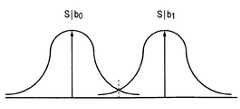
첨부도면의 도 2는, 4개의 전압 레벨을 가져 2 비트의 데이터를 표시할 수 있는 MLC에 의해 기억되는 전압 레벨을 개략적으로 예시한 것이다. 도시된 것과 같이, 단조 증가하는 2 비트 수를 표시하기 위해 서로 다르게 증가하는 전압 레벨을 사용한다. 전압이 감지될 때 기억 또는 판독 에러가 발생할 수 있으며, 이 결과 전압 레벨이 인접한 전압 레벨들 중에서 한 개에 대응하는 것으로 틀리게 감지된다. 또한, MLC의 완전한 방전이나 판독값이 인접한 값 이외의 값을 갖게 하는 에러 등의 다른 에러가 발생하는 일이 일어날 수 있다.Fig. 2 of the accompanying drawings schematically illustrates the voltage levels stored by the MLC, which can display two bits of data with four voltage levels. As shown, differently increasing voltage levels are used to indicate the monotonically increasing number of two bits. Memory or read errors can occur when a voltage is detected, which results in a wrong sense that the voltage level corresponds to one of the adjacent voltage levels. In addition, other errors may occur such as complete discharge of the MLC or an error that causes the readout to have a value other than the adjacent value.
플래시 셀 내부의 이와 같은 에러를 해결하기 위해, 판독 경로 내부에 에러정정 메카니즘을 제공하는 것이 알려져 있다. 첨부도면의 도 3은 이와 같은 배치를 나타낸 것이다. 도 3의 시스템에서는, 집적회로 플래시 메모리(14)가 프로세서(16)에 접속된다. 프로세서(16)는 플래시 메모리(14) 내부에 데이터 값을 기억하고 플래시 메모리(14)에서 데이터 값을 판독할 수 있다. 플래시 메모리(14)는 플래시 메모리 셀들(20)의 어레이(18)를 포함한다. 이와 같은 어레이(18)는, 프로세서(16)에 의해 기록된 데이터 값들을 기억하는 부분(22)과, 에러정정 코드를 기억하는 부분(24)을 포함한다. 에러정정 코드(ECC) 코드어는 프로세서(16)와 어레이(18) 사이의 데이터 경로에 배치된 에러정정회로(26)에 의해 기록된다. 에러정정 코드는 보통 코드어들이 원본 데이터인 계통적인 코드로서, 기억된 데이터가 기록될 때 패리티 데이터가 이 기억된 데이터에 추가되고, 기억된 데이터를 판독할 때 코드어들을 사용하여, 기억된 데이터 내부의 에러를 검출하고, 이 검출된 에러가 에러정정 코드에 의해 정정할 수 있는 능력 내에 해당하면(예를 들어, 에러가 너무 광범위하지 않으면) 이 검출된 에러를 정정한다. 다수의 개별적인 플래시 셀들이 결함을 갖고 있더라도, 이와 같은 메카니즘은, ECC 보호된 NAND(14)와 인터페이스로 연결된 프로세서(16)의 데이터 수신부(data sink)에 의해 관찰될지도 모르는 판독 에러의 통계적인 확률을 허용가능한 레벨로 줄일 수 있다.In order to solve such an error in the flash cell, it is known to provide an error correction mechanism inside the read path. 3 of the accompanying drawings shows such an arrangement. In the system of FIG. 3, an integrated
도 3에 도시된 시스템의 문제점은, 에러정정 코드 기억 부분(24) 내부에의 에러정정 코드에 대한 기억 요구로 인해 불리한 기억 오버헤드가 나타나 유용한 데이터를 기억하기 위한 어레이(18)의 전체 용량을 줄인다는 것이다. 적절한 에러정정을 제공하기 위해 기억할 필요가 있는 에러정정 코드의 양을 줄일 수 있는 조치는, 이러한 조치가 어레이(18) 내부의 저장 용량을 프로세서(16)에 의해 기록 및 판독할 작업 데이터를 기억하는데 사용될 수 있도록 하기 때문에 유리하다. 도 3의 시스템의 또 다른 문제점은, 에러정정 메카니즘(26)이 불리한 지연시간(latency)을 어레이(16)로부터의 판독 및 기록 동작에 도입하여, 시스템 성능을 악화시킨다는 것이다. 더구나, 에러정정 메카니즘(26)이 비교적 크고 복잡하여, 시스템의 크기, 비용 및 액세스 속도를 불리하게 증가시킬 수 있다. 데이터 무결성을 유지하면서, 플래시 메모리 셀의 에러정정 요구와 관련된 오버헤드를 줄일 수 있는 조치가 유리하다는 것을 알 수 있다.
The problem with the system shown in FIG. 3 is that the storage requirements for the error correction code inside the error correction
일면에 따르면, 본 발명은,According to one aspect, the present invention,
n-비트 심볼에 대응하는 2n 신호 기억 레벨을 각각 갖는 다중레벨 플래시 메모리 셀들의 어레이(이때, n은 1보다 큰 정수이다)와,an array of multilevel flash memory cells, each having 2n signal storage levels corresponding to n-bit symbols, where n is an integer greater than 1, and
상기 어레이에 접속되고, 상기 n-비트 심볼들의 세트에 대해 에러정정을 행하도록 구성된 에러정정회로를 구비하고,An error correction circuit connected to the array and configured to perform error correction on the set of n-bit symbols,
상기 에러정정회로는 상기 n-비트 심볼들의 심볼 에러 특성들에 부합하는 에러정정을 행하고, 상기 심볼 에러 특성들은 상기 셀들의 1개 이상의 물리적 특성들에 의해 결정되는 집적회로를 제공한다.The error correction circuit provides error correction that matches the symbol error characteristics of the n-bit symbols, and the symbol error characteristics provide an integrated circuit determined by one or more physical characteristics of the cells.
본 발명의 기술은, 다중레벨 플래시 메모리 셀이 n-비트 심볼에 대응하는 2n 신호 기억 레벨을 갖고 사용되고 있을 때(이때, n은 1보다 큰 정수이다), 메모리 셀에서 판독된 신호 기억 레벨들이 n-비트 심볼들의 심볼 에러 특성들에 부합하는 에러정정을 사용한 n-비트 심볼들로서 취급되는 경우에, 사용되고 있는 에러정정회로의 효율 및/또는 유효성이 증가할 수 있다는 인식을 갖는다. 이에 반해, 종래의 시스템에서는, 셀의 물리적 특성들에 의해 제어되는 심볼 에러 특성들에 맞추어 에러정정 메카니즘을 부합하는 것에 상관없이 판독된 데이터 내부의 에러가 독립적인 에러로 취급된다. 심볼 에러 특성들에 대해 에러정정 메카니즘을 부합시킴으로써, 발생할 것 같이 않은 에러를 정정하기 위해 여분의(redundant) 용량을 제공하지 않고, 에러정정 메카니즘이 통계적으로 발생할 것 같은 에러를 더 잘 정정할 수 있다. 그 결과, 동일한 에러 보호 수준을 달성하기 우 l해 기억할 필요가 있는 에러정정 코드 패리티 데이터 오버헤드의 양을 줄일 수 있으며, 및/또는 크기 및/또는 지연시간과 관련하여, 에러정정 메카니즘과 연관된 하드웨어 오버헤드를 줄일 수 있다.The technique of the present invention is that when a multilevel flash memory cell is being used with a 2n signal storage level corresponding to an n-bit symbol, where n is an integer greater than 1, the signal storage levels read from the memory cell are When treated as n-bit symbols with error correction that matches the symbol error characteristics of the n-bit symbols, one has the recognition that the efficiency and / or effectiveness of the error correction circuit being used may increase. In contrast, in conventional systems, errors within the read data are treated as independent errors, regardless of conforming error correction mechanisms to symbol error characteristics controlled by the cell's physical characteristics. By matching error correction mechanisms for symbol error characteristics, it is possible to better correct errors that are likely to occur statistically, without providing redundant capacity to correct errors that are unlikely to occur. . As a result, it is possible to reduce the amount of error correction code parity data overhead that needs to be remembered to achieve the same level of error protection, and / or hardware associated with the error correction mechanism in terms of size and / or latency. Overhead can be reduced.
어레이로부터 판독된 n-비트 심볼들을 m개의 이들 n-비트 심볼들의 세트들로 처리하도록 에러정정회로를 구성하는 것이 간편한데, 이때 m은 1보다 정수이다. 다중레벨 플래시 셀에서 판독된 정수의 n-비트 심볼들을 포함하는 데이터에 대해 연산을 하여 에러를 정정함으로써, 더 높은 에러정정 효율을 얻을 수 있다.It is easy to configure the error correction circuit to process the n-bit symbols read from the array into m sets of these n-bit symbols, where m is an integer greater than one. By operating on data containing integer n-bit symbols read in a multilevel flash cell to correct the error, higher error correction efficiency can be obtained.
n-비트 심볼들은 k 세트들을 포함하는 프레임으로서 어레이로부터 간편하게 판독되어도 되는데, 이때 각각의 세트는 m개의 n-비트 심볼들을 포함하고, m*n이 한 프레임의 어드레스 공간을 정의하므로, n이 2n*m보다 작다. 프레임은 패리티 심볼들과 데이터 심볼들을 포함한다(따라서, 패리티 데이터가 포함될 때, 프레임 크기가 2n*n을 초과할 수도 있지만, 심볼들의 세트들은 여전히 프레임으로 어드레스 지정가능하게 된다).The n-bit symbols may simply be read from the array as a frame containing k sets, where each set contains m n-bit symbols, where m * n defines the address space of one frame, so n equals 2 less thann * m The frame includes parity symbols and data symbols (hence, when parity data is included, the frame size may exceed 2n * n , but the sets of symbols are still addressable to the frame).
m개의 n-비트 심볼들의 세트들에 대해 행해지는 에러정정은 리드 솔로몬(RS) 대수 에러정정인 것이 바람직한데, 이와 같이 구성하면 워드 크기가 에러정정의 효율을 증가시키도록 정수의 심볼들과 일치하기 때문이다.The error correction performed on the set of m n-bit symbols is preferably Reed-Solomon (RS) algebraic error correction, where such a word size matches the integer symbols to increase the efficiency of the error correction. Because.
플래시 메모리 셀들은, 플래시 메모리의 특정한 기술에 의존하여 NAND 플래시 메모리 셀 또는 NOR 플래시 메모리 셀이 될 수도 있다.Flash memory cells may be NAND flash memory cells or NOR flash memory cells depending on the particular technology of flash memory.
또 다른 일면에 따르면, 집적회로는,According to another aspect, an integrated circuit,
n-비트 심볼에 대응하는 2n 신호 기억 레벨을 각각 갖는 다중레벨 플래시 메모리 셀 수단들의 어레이(이때, n은 1보다 큰 정수이다)와,an array of multilevel flash memory cell means each having 2n signal storage levels corresponding to n-bit symbols, where n is an integer greater than 1, and
상기 어레이에 접속되어, 상기 n-비트 심볼들의 세트에 대해 에러정정을 행하는 에러정정수단을 구비하고,An error correction means connected to said array for performing error correction on said set of n-bit symbols,
상기 에러정정수단은 상기 n-비트 심볼들의 심볼 에러 특성들에 부합하는 에러정정을 행하고, 상기 심볼 에러 특성들은 상기 셀 수단들의 1개 이상의 물리적 특성들에 의해 결정된다.The error correction means performs error correction that matches the symbol error characteristics of the n-bit symbols, wherein the symbol error characteristics are determined by one or more physical characteristics of the cell means.
또 다른 일면에 따르면, 집적회로 내부의 데이터를 액세스하는 방법은,According to yet another aspect, a method of accessing data inside an integrated circuit includes:
n-비트 심볼에 대응하는 2n 신호 기억 레벨을 각각 갖는 다중레벨 플래시 메모리 셀들의 어레이 내부에 데이터를 기억하는 단계(이때, n은 1보다 큰 정수이다)와,storing data in an array of multilevel flash memory cells, each having a 2n signal storage level corresponding to an n-bit symbol, where n is an integer greater than one;
상기 어레이로부터 n-비트 심볼들의 세트를 판독하는 단계와,Reading a set of n-bit symbols from the array;
상기 세트에 대해 에러정정을 행하는 단계를 포함하고,Performing error correction on the set,
상기 에러정정은 상기 n-비트 심볼들의 심볼 에러 특성들에 부합되고, 상기 심볼 에러 특성들은 상기 셀들의 1개 이상의 물리적 특성들에 의해 결정된다.The error correction corresponds to symbol error characteristics of the n-bit symbols, and the symbol error characteristics are determined by one or more physical characteristics of the cells.
또 다른 일면에 따르면, 집적회로는According to another aspect, an integrated circuit
2n 신호 기억 레벨을 각각 갖는 다중레벨 플래시 메모리 셀들의 어레이(이때, n은 1보다 큰 정수이다)와,An array of multilevel flash memory cells, each having a 2n signal storage level, where n is an integer greater than 1, and
상기 어레이에 접속되고, 액세스되고 있는 셀로부터 신호를 판독하여 상기 신호를 표시하는 n 비트의 데이터를 생성하도록 구성된 프리코딩회로와,A precoding circuit connected to the array and configured to read a signal from a cell being accessed to generate n bits of data representing the signal;
상기 프리코딩회로에 접속되고, 상기 프리코딩회로에서 판독된 상기 n 비트의 데이터에 대해 에러정정을 행하도록 구성된 에러정정회로를 구비하고,An error correction circuit connected to the precoding circuit and configured to perform error correction on the n bits of data read by the precoding circuit,
상기 프리코딩회로는, 상기 n 비트의 데이터 내부의 비트 에러들 사이의 독립성을 증가시키는 매핑을 사용하여 상기 셀로부터의 상기 신호를 상기 n 비트의 데이터에 매핑하고,The precoding circuit maps the signal from the cell to the n bits of data using a mapping that increases independence between bit errors within the n bits of data,
상기 에러정정회로에 의해 행해지는 상기 에러정정은 독립적인 동일한 분산된 에러 패턴들(independent identical distributed error patterns)을 타겟으로 한다.The error correction performed by the error correction circuit targets independent identical distributed error patterns.
이 기술은, 도 2에 도시된 것과 같이 비트 값에 대한 신호 기억 레벨의 단순한 단조 매핑이 발생 가능성이 높은 일부의 비트 에러들과 발생 가능성이 거의 없는 일부의 비트 에러들을 생성하도록 다양한 기억 레벨들과 연관된 에러가 존재하는, 2n 신호 기억 레벨들을 각각 갖는(이때, n은 1보다 큰 정수이다) 다중레벨 플래시 메모리 셀의 물리적인 특성이 제공되는 에러정정 능력과 자원을 비효율적으로 사용한다는 것을 인식하고 있다. 본 기술은, 이와 같은 문제를 인식하여, 어레이에 접속되어 기억 셀로부터 신호를 판독하고, 발생되는 n 비트의 데이터 내부의 비트 에러들 사이의 독립성을 증가시키는 매핑을 사용하여 이 신호를 표시하는 n 비트의 데이터를 생성하는 프리코딩회로를 설치함으로써, 이 문제를 해소한다. 신호 기억 레벨과 n-비트 데이터 값 사이의 단조 관계와 비교할 때 이와 같이 증가된 비트 에러의 독립성으로 인해, 에러정정회로에 행해진 에러정정이 효율의 손실없이 독립적인 분산된 에러 패턴들을 타겟으로 하여도 된다.This technique uses a variety of storage levels such that a simple monotonic mapping of the signal storage level to the bit value, as shown in FIG. Recognizing that the physical characteristics of a multilevel flash memory cell, each having 2n signal storage levels, where n is an associated error, are inefficient use of error correction capabilities and resources provided have. The present technology recognizes this problem, and n is connected to the array to read the signal from the memory cell and display this signal using a mapping that increases the independence between bit errors within the n bits of data generated. This problem is eliminated by providing a precoding circuit that generates bit data. Due to this increased bit error independence compared to the monotonic relationship between the signal memory level and the n-bit data value, even if error corrections made to the error correction circuit target independent distributed error patterns without loss of efficiency do.
프리코딩회로에 의해 채용된 매핑은, 신호의 n-비트 데이터로의 그레이 코딩(Gray coding)이어도 된다.The mapping employed by the precoding circuit may be gray coding of the signal into n-bit data.
n의 값은 변동될 수 있지만, 바람직하게는 2, 3 및 4 중에서 한 개다.The value of n can vary, but is preferably one of 2, 3 and 4.
사용된 에러정정의 형태도 변동될 수 있지만, 본 발명의 기술은, Bose Ray-Chaudhuri Hocquenghem(BCH) 에러정정 코드 등의 대수 에러코딩에 매우 적합하다.Although the form of error correction used may vary, the technique of the present invention is well suited for algebraic error coding, such as Bose Ray-Chaudhuri Hocquenghem (BCH) error correction codes.
플래시 메모리 셀은 구현에 따라 NAND 플래시 메모리 셀 또는 NOR 플래시 메모리 셀이어도 된다.The flash memory cell may be a NAND flash memory cell or a NOR flash memory cell, depending on the implementation.
또 다른 일면에 따르면, 본 발명은,According to another aspect, the present invention,
2n 신호 기억 레벨을 각각 갖는 다중레벨 플래시 메모리 셀 수단들의 어레이(이때, n은 1보다 큰 정수이다)와,An array of multilevel flash memory cell means each having 2n signal storage levels, where n is an integer greater than 1, and
상기 어레이에 접속되고, 액세스되고 있는 셀 수단으로부터 신호를 판독하여 상기 신호를 표시하는 n 비트의 데이터를 생성하는 프리코딩수단과,Precoding means connected to said array for reading a signal from a cell means being accessed to generate n bits of data representing said signal;
상기 프리코딩수단에 접속되고, 상기 프리코딩수단에서 판독된 상기 n 비트의 데이터에 대해 에러정정을 행하는 에러정정수단을 구비하고,An error correction means connected to said precoding means and performing error correction on said n bits of data read by said precoding means,
상기 프리코딩수단은, 상기 n 비트의 데이터 내부의 비트 에러들 사이의 독립성을 증가시키는 매핑을 사용하여 상기 셀 수단으로부터의 상기 신호를 상기 n 비트의 데이터에 매핑하고,The precoding means maps the signal from the cell means to the n bits of data using a mapping that increases independence between bit errors within the n bits of data,
상기 에러정정수단에 의해 행해지는 상기 에러정정은 독립적인 동일한 분산된 에러 패턴들을 타겟으로 하는 집적회로를 제공한다.The error correction performed by the error correction means provides an integrated circuit that targets the same distributed error patterns that are independent.
또 다른 일면에 따르면, 본 발명은, 집적회로 내부의 데이터를 액세스하는 방법으로서,According to yet another aspect, the present invention provides a method for accessing data inside an integrated circuit.
n-비트 심볼에 대응하여 2n 신호 기억 레벨을 각각 갖는 다중레벨 플래시 메모리 셀들의 어레이 내부에 데이터를 기억하는 단계(이때, n은 1보다 큰 정수이다)와,storing data in an array of multilevel flash memory cells each having 2n signal storage levels corresponding to n-bit symbols, where n is an integer greater than one;
액세스되고 있는 셀로부터 신호를 판독하는 단계와,Reading a signal from the cell being accessed;
상기 n 비트의 데이터 내부의 비트 에러들 사이의 독립성을 증가시키는 매핑을 사용하여 상기 신호를 n 비트의 데이터에 매핑하는 단계와,Mapping the signal to n bits of data using a mapping that increases independence between bit errors within the n bits of data;
상기 n 비트의 데이터에 대해 에러정정을 행하는 단계를 포함하고,Performing error correction on the n bits of data,
상기 행해진 에러정정은, 독립적인 동일한 분산된 에러 패턴들을 타겟으로 하는 방법을 제공한다.The error correction made above provides a method for targeting independent identical distributed error patterns.
본 발명의 상기한 목적, 특징 및 이점과 다른 목적, 특징 및 이점은 첨부도면과 연계하여 주어지는 이하의 실시예의 상세한 설명으로부터 명확해질 것이다.
The above objects, features and advantages of the present invention and other objects, features and advantages will become apparent from the following detailed description given in conjunction with the accompanying drawings.
도 1은 플래시 메모리 셀을 개략적으로 나타낸 것이다.
도 2는 4개의 기억 신호 레벨을 갖는 플래시 메모리 셀을 개략적으로 나타낸 것이다.
도 3은 플래시 메모리와 에러정정 메카니즘을 사용하는 시스템을 개략적으로 나타낸 것이다.
도 4는 균일 상태 보유 확률(uniform state retention probability)에 근거한 다중레벨 플래시 NAND 메모리 셀 에러 모델을 나타낸 것이다.
도 5는 가우스 분포를 갖는 노이즈에 기인한 에러의 교차 확률(cross-over probability)을 개략적으로 나타낸 것이다.
도 6은 불균일 교차 확률에 근거한 다중레벨 NAND 플래시 메모리 셀을 개략적으로 나타낸 것이다.
도 7은 플래시 메모리 어레이에서 판독된 n-비트 심볼들의 심볼 에러 특성에 부합된 에러정정 메카니즘을 갖는 집적회로를 개략적으로 나타낸 것이다.
도 8은 심볼들의 복수의 세트를 포함하는 메모리 셀들의 프레임으로서, 이때 각각의 세트가 m개의 심볼을 갖고 각각의 심볼이 n-비트 심볼인 프레임을 개략적으로 나타낸 것이다.
도 9는 도 9는 도 7에 도시된 시스템의 동작을 개략적으로 나타낸 흐름도이다.
도 10은, 플래시 메모리 어레이와, 다중 레벨 플래시 메모리 셀로부터 판독된 n-비트의 데이터 내부의 비트 에러들 사이의 독립성을 증가시키는 매핑을 적용하는 프리코딩회로를 구비한 집적회로를 개략적으로 나타낸 것이다.
도 11은 플래시 메모리 셀 내부의 다수의 신호 기억 레벨들에 적용된 그레이 코딩을 개략적으로 나타낸 것이다.
도 12는 플래시 메모리 셀과 에러정정회로의 출력 사이에 적용된 신호처리의 데이터 경로를 개략적으로 나타낸 것이다.
도 13은 도 10에 도시된 시스템의 동작을 개략적으로 나타낸 흐름도이다.1 schematically shows a flash memory cell.
2 schematically illustrates a flash memory cell having four memory signal levels.
3 schematically illustrates a system using a flash memory and an error correction mechanism.
4 illustrates a multilevel flash NAND memory cell error model based on uniform state retention probability.
5 schematically shows the cross-over probability of an error due to noise with a Gaussian distribution.
6 schematically illustrates a multilevel NAND flash memory cell based on a nonuniform crossing probability.
7 schematically illustrates an integrated circuit having an error correction mechanism that conforms to the symbol error characteristics of n-bit symbols read from a flash memory array.
8 is a frame of memory cells comprising a plurality of sets of symbols, wherein each set schematically shows a frame in which each set has m symbols and each symbol is an n-bit symbol.
9 is a flow chart schematically showing the operation of the system shown in FIG.
10 schematically shows an integrated circuit having a flash memory array and a precoding circuit that applies a mapping that increases independence between bit errors within n-bit data read from a multilevel flash memory cell. .
11 schematically illustrates gray coding applied to multiple signal storage levels within a flash memory cell.
12 schematically shows the data path of signal processing applied between the flash memory cell and the output of the error correction circuit.
FIG. 13 is a flowchart schematically illustrating the operation of the system illustrated in FIG. 10.
도 4는, 도 2에 도시된 신호 기억 레벨과 데이터 값 사이의 매핑을 사용하는 2-비트 메모리 셀에 대한 균일 상태 보유 확률에 근거한 다중레벨 NAND 플래시 메모리 셀 에러 모델을 예시한 것이다. 신호 기억 레벨과 데이터 값 사이의 이와 같은 매핑은, 자연적인 순서 {00,01,10,11}을 따르는 단조(이 경우에는 기억된 전하에 따라 증가) 관계를 나타낸다. 이와 같은 순서에 있어서는, 예를 들어 01로부터 10으로의 변화와 같이, 한 레벨로부터 다음 레벨로의 변화가 2 비트에서 에러를 일으키는 경우가 있다. 전하 손실과 전하 이동 에러에 대해, 가장 일어날 가능성이 있는 에러는 한 개의 레벨의 변화이다. 비트 에러 확률 Pe는 전이 확률 Pt에서 얻어질 수도 있다. 이 예의 4-레벨 NAND 셀에 대해서는, 도 4에 도시된 것과 같이 6가지의 가능한 레벨 전이가 존재한다. 전이 확률이 균일하다고, 즉 한 레벨 위로 변화하는 것이나 한 레벨 아래로 변화하는 것이 동일하게 일어날 수 있다고 가정하면, 도 4의 에러 모델을 적용한다. 이때, 셀 전하 손실 에러는 더 낮은 레벨로의 이동만이 일어날 가능성이 있으므로, 위와 아래로의 전이가 동등하게 발생할 것 같다는 가정은 실제로는 유효하지 않기 때문에, 이와 같은 에러 모델은 단지 근사식에 불과하다는 점을 이해하기 바란다. 그럼에도 불구하고, 하위 순서 비트가 상위 순서 비트보다 에러를 겪을 가능성이 더 크다는 것을 도 4의 에러 모델에서 알 수 있다. 이것은, 메모리 셀의 물리적 특성의 결과로서, 이 특성이 데이터를 표시하기 위해 메모리 셀에서 판독된 2-비트 심볼과 어떻게 관련되는지를 나타낸다.4 illustrates a multilevel NAND flash memory cell error model based on the uniform state retention probability for a 2-bit memory cell using the mapping between the signal storage levels and data values shown in FIG. 2. This mapping between the signal storage level and the data value represents a monotonic (in this case increasing with stored charge) relationship in the natural order {00,01,10,11}. In such a sequence, for example, a change from one level to the next level may cause an error in two bits, such as a change from 01 to 10. For charge loss and charge transfer errors, the most likely error is one level of change. The bit error probability Pe may be obtained at the transition probability Pt . For the four-level NAND cell of this example, there are six possible level transitions as shown in FIG. Assuming that the transition probabilities are uniform, ie changing up one level or changing down one level, the error model of FIG. 4 is applied. At this point, since the cell charge loss error is likely to shift only to a lower level, the assumption that transitions up and down are likely to occur equally is not valid, so this error model is only an approximation. Please understand. Nevertheless, it can be seen from the error model of FIG. 4 that the lower order bits are more likely to suffer an error than the higher order bits. This is a result of the physical characteristics of the memory cell and indicates how this characteristic relates to the 2-bit symbol read out of the memory cell to represent the data.
도 5는 데이터 송신에 대한 표준 에러 모델에 따른 가우스 노이즈로 인한 판독된 비트의 교차 확률을 개략적으로 나타낸 것이다. 정보 비트 b는, 서로 다른 신호 기억 레벨에 매핑된 2가지 상태, 즉 b0 및 b1을 가질 수 있다. 판독후에 수신된 심볼은 어느 한쪽의 레벨과 부가적인 노이즈에 의해 정의된 값을 취한다. 노이즈는 보통 가우스 분포이다. 이와 같은 시나리오에서, 바람직한 판정 임계값은 이들 2개의 레벨 사이의 중간점에 해당한다. 비트 에러 확률은, 기억된 신호 값이 사실상 b1일 때의 b0를 결정하는 확률과, 기억된 신호 값이 b0일 때의 b1을 결정하는 확률의 합이다. 이것은 가우스 확률 밀도 함수의 꼬리 부분 아래의 적분에 해당한다. 이때, 이와 같은 교차는 한 방향으로만 계수해야 한다는 점에 주목하기 바란다. 더 많은 레벨에서는, 내부 레벨들이 2 방향으로 교차할 수 있으며, 사실상 다수의 레벨을 교차할 수 있다(그러나, 확률이 매우 낮다). 전이 확률 Pt를 사용하는 도 1의 모델과 관련하여, 다중 레벨 에러 모델이 도 6에 도시된 것과 같이 되는데, 이때에는 내부 및 외부 레벨들 사이의 전이 에러에서 차이점을 갖는다. 이때, 이와 같은 에러 모델은 근사식에 지나지 않지만, 도 5에 도시된 각각의 개별적인 기억 레벨에 대해 더 양호하게 들어맞는 확률 밀도 함수(Probability Density Function: PDF)를 정의함으로써 이러한 근사를 향상시킬 수 있다는 것이 명백하다.5 schematically illustrates the probability of intersection of read bits due to Gaussian noise according to a standard error model for data transmission. The information bit b may have two states mapped to different signal storage levels, namely b0 and b1 . The symbol received after reading takes the value defined by either level and additional noise. Noise is usually a Gaussian distribution. In such a scenario, the preferred decision threshold corresponds to the midpoint between these two levels. A bit error probability, the sum of the probability of determining the probability of b1 when the stored signal value is determined for the time of b0 b1 and in effect, the stored signal value b0 days. This corresponds to the integral under the tail of the Gaussian probability density function. Note that this intersection must be counted in only one direction. At more levels, the inner levels can cross in two directions, and in fact can cross multiple levels (but the probability is very low). With respect to the model of FIG. 1 using the transition probability Pt , the multi-level error model is as shown in FIG. 6, with the difference in transition error between the inner and outer levels. This error model is only an approximation, but this approximation can be improved by defining a better density probability function (PDF) for each individual memory level shown in FIG. It is obvious.
도 7은 다중레벨 플래시 메모리 셀(32)의 어레이(30)를 구비한 적분회로(28)를 나타낸 것이다. 이들 플래시 메모리 셀 각각은 2n 신호 기억 레벨들 중 한 개에 대응하고 판독할 때의 n-비트 심볼에 대응하는 전하를 저장하며, 이때 n은 1보다 큰 정수이다. 보다 구체적 실시예에서는, n이 2, 3 또는 4일 수 있다. n의 이와 같은 값들은 각각 4, 8 및 16 신호 기억 레벨을 갖는 셀을 제공한다.7 shows an integrating
어레이(30)는 데이터 값들과 에러정정 코드들을 기억한다. 이들 에러정정 코드는 리드 솔로몬 코드이다.
에러정정회로(34)는, 어레이(30)에 접속되어 어레이(30) 내부의 플래시 메모리 셀(32)에 대해 데이터 값들을 판독 및 기록하는 역할을 한다. 메모리 셀들(32)이 전술한 것과 같이 다중레벨 메모리 셀이므로, N-비트 심볼들을 사용하여 데이터 셀들이 기록 및 판독되며, 이때 n은 1보다 크다. 도 7에 도시된 예는, 3-비트 심볼 [abc]가 어레이(30)에서 판독되고 있는 것을 나타내고 있다.The error correction circuit 34 is connected to the
도 4, 도 5 및 도 6과 관련하여 이전에 설명한 것과 같이, 메모리 셀들(32)의 물리적 특성은, n-비트 심볼들 내에서 서로 다른 비트 값들 사이에서 불균일한 n-비트 신볼들의 심볼 에러 특성을 제공한다. 일례로, 특정한 비트의 심볼들이 다른 비트들보다 에러를 더 겪기 쉬울 수도 있다. 에러정정회로(34)는, 어떤 어레이(30)가 액세스되는지와 심볼들의 에러 특성을 이용하여 심볼들을 매칭(match)하도록 구성되고 동작한다. 에러정정회로는 이들 심볼의 세트들에 대해 에러정정을 형성한다. n-비트 심볼의 에러 확률은 n-비트 심볼을 구성하는 비트들의 비트에러 확률보다 낮다.As previously described with respect to FIGS. 4, 5, and 6, the physical characteristics of the
도 8에 도시된 것과 같이, 심볼들의 세트는 m개의 n-비트 심볼들을 포함한다. 도시된 것과 같이, 이것은 12-비트 워드를 생성하는 4개의 3-비트 심볼들에 대응한다. 이와 같은 12-비트 워드는, 마찬가지로 어레이(30) 내부에 기억된 에러정정 코드들을 사용하여 12-비트 리드 솔로몬 에러정정을 겪는다. 심볼들의 세트들은 어레이(30)로부터 프레임들로 판독되며, 이때 각 프레임은 k개의 세트들을 포함하고, 각각의 세트는 m개의 n-비트 심볼들을 포함한다.As shown in FIG. 8, the set of symbols includes m n-bit symbols. As shown, this corresponds to four 3-bit symbols that produce a 12-bit word. This 12-bit word likewise undergoes 12-bit Reed Solomon error correction using error correction codes stored within the
에러들이 놓인 어드레스 공간이 줄어들어 회로의 비트 폭을 더 좁게 만들고 이 어드레스 공간 내에서의 검색 속도를 더 빠르게 하므로, 리드 솔로몬(심볼 기반의) 코드들의 사용은 에러정정회로의 크기와 비용을 줄이는 역할을 한다. 리드 솔로몬 코드가 에러를 갖는 심볼이 검출될 때 에러 값의 계산을 필요로 하지만, 더 큰 검색 공간의 비용과 달리, 이와 같은 계산은 선형적인 비용만을 초래한다.The use of Reed Solomon (symbol based) codes reduces the size and cost of the error correction circuit, as the address space where errors are placed is reduced, which makes the bit width of the circuit narrower and speeds up the search within this address space. do. Although the Reed Solomon code requires the calculation of an error value when a symbol with an error is detected, unlike the cost of a larger search space, such a calculation results in a linear cost only.
이 예에서, 메모리 셀들(32)는 NAND 메모리 셀이다. NOR 플래시 메모리 셀이 사용될 수도 있다.In this example, the
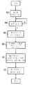
도 9는 도 7의 시스템의 동작을 개략적으로 나타낸 흐름도이다. 스텝 36에서, 다중레벨 플래시 메모리 셀(32)에 데이터가 기억된다. 스텝 38에서는, 판독 요구가 행해질 때까지 처리를 대기한다. 판독 요구가 행해지면, 스텝 40에서는 n-비트 심볼들의 프레임을 판독한다. 이들 n-비트 심볼들은, m개의 n-비트 심볼들을 각각 포함하는 세트들과 같이 세트들로 그룹으로 나뉜다. 그후, 이들 심볼들의 세트들은 스텝 42에서 리드 솔로몬 에러정정을 겪는다. 그후, 스텝 44에서, 에러정정이 행해진 출력 데이터를 프로세서, 또는 다른 장치로 출력한다.9 is a flow chart schematically illustrating the operation of the system of FIG. In step 36, data is stored in the multilevel
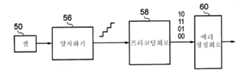
도 10은 또 다른 집적회로(46)를 나타낸 것이다. 집적회로(46)는 메모리 셀들(50)의 어레이(48)를 포함한다. 프리코딩회로(52)가 어레이(48)에 접속되어 (NAND 또는 NOR MLC 등일 수 있는) 메모리 셀들(50)에 대해 판독 및 기록을 하는 역할을 한다. 에러정정회로(54)는 판독되는 각각의 메모리 셀(50)에 대해 프리코더(52)로부터 N-비트의 데이터를 수신한다.10 shows another
도 11은, 메모리 셀들(50)의 신호 기억 레벨들과, 프리코딩회로(52)에 의해 매핑될 때 이들 레벨이 표시하는 데이터 값들 사이의 관계를 나타낸 것이다. 특히, 프리코딩회로(52)는 기억 신호 레벨들을 전압(전하)의 오름차순으로 2-비트 데이터 값들 00, 01, 11 및 10에 매핑한다. 이것은 그레이 코딩이다. 이때, 이것은 사용할 수 있는 그레이 코딩의 단지 일례에 지나지 않으며 다른 매핑이 사용가능하다는 것은 자명하다.FIG. 11 shows the relationship between the signal storage levels of the
프리코딩회로(52)에 의해 행해지는 매핑은, 메모리 셀(50)에서 판독된 데이터의 비트들 내부의 비트 에러들 사이의 독립성을 증가시키는 역할을 한다. 특히, 이 예에서는, 매핑을 적용한 결과, 생성된 비트 에러들이 독립적인 동일한 분산된 에러 패턴들을 더 가깝게 닮게 된다. 따라서, 애러정정회로(54)는, 이 에러정정회로가 행하는 에러정정에 있어서 이와 같은 독립적인 동일한 분산된 에러 패턴들을 타겟으로 삼는다. 이와 같은 에러를 타겟으로 하여 행해지는 에러정정의 한가지 예로는 Bose Ray-Chaudhuri Hocquenghem(BCH) 코드를 들 수 있다. 이와 같은 BCH 코드는, 독립적인 동일한 분산된 에러 패턴들에는 매우 적합하지만, 도 2와 도 4, 도 5 및 도 6에 따라 액세스할 때 메모리 셀들과 관련된 불균일 심볼 에러 특성들의 형태에 대해서는 덜 적합하다. 프리코딩회로(52)의 역할은, 에러정정 메카니즘이 에러 패턴들을 효율적으로 취급할 수 있도록, 기억 신호 레벨들이 독립적인 동일한 분산된 에러 패턴들에 더 긴밀하게 대응하도록 이들 기억 신호 레벨들을 매핑하는 것이다.The mapping done by the
도 12는 플래시 메모리 셀(50)을 판독시의 신호 경로를 개략적으로 나타낸 것이다. 양자화회로(56)는, 셀(50)로부터 기억 신호 레벨을 판독하고, 소정의 개별적인 전압 레벨의 양자화된 출력을 발생하는 역할을 한다. 프리코딩회로(58)는 이와 같은 양자화된 시호와 그레이 코드를 판독하여 2 비트의 데이터에 대응하는 2-비트 출력을 제공한다. 그후, 이들 데이터 비트는 에러정정회로(60)로 전달되어, BCH 에러정정을 겪게 된다.12 schematically shows the signal path when reading the
도 13은 도 10에 도시된 시스템의 동작을 나타낸 흐름도이다. 스텝 62에서는, 다중비트 데이터 값들을 포함하는 데이터 값들이 플래시 메모리 셀들에 기억된다. 스텝 64에서는, 판독이 요구되는 것을 시스템이 대기한다. 스텝 66에서는, 기억 신호값이 해당 메모리 셀에서 판독되어, 소정 수의 레벨들 중에서 한 개로 양자화된다. 스텝 68에서는, 프리코딩회로가 양자화된 신호들을 프리코드하여 그레이 코드를 생성한다. 스텝 70에서는, 에러정정회로가 프리코딩회로에서 출력된 프리코드된 데이터에 대해 BCH 에러정정을 행한다. 스텝 72에서는, 필요에 따라 에러정정이 된 판독된 데이터가 집적회로에서 출력된다.13 is a flowchart illustrating the operation of the system shown in FIG. In
첨부도면을 참조하여 본 발명의 예시적인 실시예를 상세히 설명하였지만, 본 발명은 이들 실시예에 한정되지 않으며, 첨부된 특허청구범위에 정의된 본 발명의 보호범위 및 사상을 벗어나지 않으면서 본 발명이 속한 기술분야의 당업자에 의해 다양한 변화 및 변형이 이루어질 수 있다.While the exemplary embodiments of the present invention have been described in detail with reference to the accompanying drawings, the present invention is not limited to these embodiments, and the present invention may be made without departing from the scope and spirit of the present invention as defined in the appended claims. Various changes and modifications can be made by those skilled in the art.
Claims (16)
Translated fromKorean상기 어레이에 접속되고, 상기 n-비트 심볼들의 세트에 대해 에러정정을 행하도록 구성된 에러정정회로를 구비하고,
상기 에러정정회로는 상기 n-비트 심볼들의 심볼 에러 특성들에 부합하는 에러정정을 행하고, 상기 심볼 에러 특성들은 상기 셀들의 1개 이상의 물리적 특성들에 의해 결정되는, 집적회로.
an array of multilevel flash memory cells, each having 2n signal storage levels corresponding to n-bit symbols, where n is an integer greater than 1, and
An error correction circuit connected to the array and configured to perform error correction on the set of n-bit symbols,
Wherein the error correction circuit performs error correction that matches symbol error characteristics of the n-bit symbols, wherein the symbol error characteristics are determined by one or more physical characteristics of the cells.
상기 n-비트 심볼의 에러 확률이 상기 n-비트 심볼을 구성하는 비트들의 비트에러 확률보다 낮은, 집적회로.
The method of claim 2,
And an error probability of the n-bit symbol is lower than a bit error probability of the bits constituting the n-bit symbol.
상기 에러정정회로는, 상기 어레이로부터 판독된 n-비트 심볼들을 m개의 이들 n-비트 심볼들의 세트들로 처리하고, 이때 m은 1보다 정수인, 집적회로,The method of claim 1,
The error correction circuit processes the n-bit symbols read from the array into m sets of these n-bit symbols, where m is an integer greater than one;
상기 에러정정회로는, m개의 상기 n-비트 심볼들의 상기 세트들을 m개의 상기 n-비트 심볼들의 k개의 상기 세트들로 구성된 프레임들로서 처리하고, 이때, k는 2n*m보다 작은, 집적회로.
The method of claim 3, wherein
The error correction circuit processes the sets of m n-bit symbols as frames consisting of k the sets of m n-bit symbols, where k is less than 2n * m. .
상기 에러정정회로는, 상기 세트들 각각에 대해 리드 솔로몬 에러정정을 행하는, 집적회로.
The method of claim 3, wherein
And the error correction circuit performs Reed Solomon error correction on each of the sets.
상기 셀은,
NAND 플래시 메모리 셀과,
NOR 플래시 메모리 셀 중에서 한 개인, 집적회로.
The method of claim 1,
The cell,
NAND flash memory cells,
One of the NOR flash memory cells, integrated circuit.
상기 어레이에 접속되어, 상기 n-비트 심볼들의 세트에 대해 에러정정을 행하는 에러정정수단을 구비하고,
상기 에러정정수단은 상기 n-비트 심볼들의 심볼 에러 특성들에 부합하는 에러정정을 행하고, 상기 심볼 에러 특성들은 상기 셀 수단들의 1개 이상의 물리적 특성들에 의해 결정되는, 집적회로.
an array of multilevel flash memory cell means each having 2n signal storage levels corresponding to n-bit symbols, where n is an integer greater than 1, and
An error correction means connected to said array for performing error correction on said set of n-bit symbols,
And the error correction means performs error correction corresponding to symbol error characteristics of the n-bit symbols, wherein the symbol error characteristics are determined by one or more physical characteristics of the cell means.
n-비트 심볼에 대응하는 2n 신호 기억 레벨을 각각 갖는 다중레벨 플래시 메모리 셀들의 어레이 내부에 데이터를 기억하는 단계(이때, n은 1보다 큰 정수이다)와,
상기 어레이로부터 n-비트 심볼들의 세트를 판독하는 단계와,
상기 세트에 대해 에러정정을 행하는 단계를 포함하고,
상기 에러정정은 상기 n-비트 심볼들의 심볼 에러 특성들에 부합되고, 상기 심볼 에러 특성들은 상기 셀의 1개 이상의 물리적 특성들에 의해 결정되는, 데이터 액세스 방법.
A method of accessing data inside an integrated circuit,
storing data in an array of multilevel flash memory cells, each having a 2n signal storage level corresponding to an n-bit symbol, where n is an integer greater than one;
Reading a set of n-bit symbols from the array;
Performing error correction on the set,
Wherein the error correction corresponds to symbol error characteristics of the n-bit symbols, wherein the symbol error characteristics are determined by one or more physical characteristics of the cell.
상기 어레이에 접속되고, 액세스되고 있는 셀로부터 신호를 판독하여 상기 신호를 표시하는 n 비트의 데이터를 생성하도록 구성된 프리코딩회로와,
상기 프리코딩회로에 접속되고, 상기 프리코딩회로에서 판독된 상기 n 비트의 데이터에 대해 에러정정을 행하도록 구성된 에러정정회로를 구비하고,
상기 프리코딩회로는, 상기 n 비트의 데이터 내부의 비트 에러들 사이의 독립성을 증가시키는 매핑을 사용하여 상기 셀로부터의 상기 신호를 상기 n 비트의 데이터에 매핑하고,
상기 에러정정회로에 의해 행해지는 상기 에러정정은 독립적인 동일한 분산된 에러 패턴들을 타겟으로 하는, 집적회로.
An array of multilevel flash memory cells, each having a 2n signal storage level, where n is an integer greater than 1, and
A precoding circuit connected to the array and configured to read a signal from a cell being accessed to generate n bits of data representing the signal;
An error correction circuit connected to the precoding circuit and configured to perform error correction on the n bits of data read by the precoding circuit,
The precoding circuit maps the signal from the cell to the n bits of data using a mapping that increases independence between bit errors within the n bits of data,
Wherein the error correction performed by the error correction circuit targets the same distributed error patterns that are independent.
상기 매핑은 상기 신호의 상기 n 비트의 데이터로의 그레이 코딩인, 집적회로.
The method of claim 9,
And the mapping is gray coding of the n bits of data of the signal.
n은 2, 3 및 4 중에서 한 개인, 집적회로.
The method of claim 9,
n is one of 2, 3 and 4, integrated circuit.
상기 에러정정은, n 비트의 데이터의 복수의 세트들을 포함하는 소정의 프레임에 대해 행해지는 대수 에러정정 코딩인, 집적회로.
The method of claim 9,
And the error correction is logarithmic error correction coding performed on a predetermined frame comprising a plurality of sets of n bits of data.
상기 대수 에러정정 코딩은 BCH 에러정정 코딩인, 집적회로.
The method of claim 12,
And the logarithmic error correction coding is BCH error correction coding.
상기 셀은,
NAND 플래시 메모리 셀과,
NOR 플래시 메모리 셀 중에서 한 개인, 집적회로.
The method of claim 9,
The cell,
NAND flash memory cells,
One of the NOR flash memory cells, integrated circuit.
상기 어레이에 접속되고, 액세스되고 있는 셀 수단로부터 신호를 판독하여 상기 신호를 표시하는 n 비트의 데이터를 생성하는 프리코딩수단과,
상기 프리코딩수단에 접속되고, 상기 프리코딩수단에서 판독된 상기 n 비트의 데이터에 대해 에러정정을 행하는 에러정정수단을 구비하고,
상기 프리코딩수단은, 상기 n 비트의 데이터 내부의 비트 에러들 사이의 독립성을 증가시키는 매핑을 사용하여 상기 셀 수단으로부터의 상기 신호를 상기 n 비트의 데이터에 매핑하고,
상기 에러정정수단에 의해 행해지는 상기 에러정정은 독립적인 동일한 분산된 에러 패턴들을 타겟으로 하는, 집적회로.
An array of multilevel flash memory cell means each having 2n signal storage levels, where n is an integer greater than 1, and
Precoding means connected to the array and reading out a signal from the cell means being accessed to generate n bits of data representing the signal;
An error correction means connected to said precoding means and performing error correction on said n bits of data read by said precoding means,
The precoding means maps the signal from the cell means to the n bits of data using a mapping that increases independence between bit errors within the n bits of data,
Wherein said error correction made by said error correction means targets the same distributed error patterns that are independent.
n-비트 심볼에 대응하여 2n 신호 기억 레벨을 각각 갖는 다중레벨 플래시 메모리 셀들의 어레이 내부에 데이터를 기억하는 단계(이때, n은 1보다 큰 정수이다)와,
액세스되고 있는 셀로부터 신호를 판독하는 단계와,
상기 n 비트의 데이터 내부의 비트 에러들 사이의 독립성을 증가시키는 매핑을 사용하여 상기 신호를 n 비트의 데이터에 매핑하는 단계와,
상기 n 비트의 데이터에 대해 에러정정을 행하는 단계를 포함하고,
상기 행해진 에러정정은, 독립적인 동일한 분산된 에러 패턴들을 타겟으로 하는, 데이터 액세스 방법.A method of accessing data inside an integrated circuit,
storing data in an array of multilevel flash memory cells each having 2n signal storage levels corresponding to n-bit symbols, where n is an integer greater than one;
Reading a signal from the cell being accessed;
Mapping the signal to n bits of data using a mapping that increases independence between bit errors within the n bits of data;
Performing error correction on the n bits of data,
The error correction made is targeted to the same distributed error patterns that are independent.
Applications Claiming Priority (2)
| Application Number | Priority Date | Filing Date | Title |
|---|---|---|---|
| US12/585,353US8386890B2 (en) | 2009-09-11 | 2009-09-11 | Error correction for multilevel flash memory |
| US12/585,353 | 2009-09-11 |
Publications (1)
| Publication Number | Publication Date |
|---|---|
| KR20110028228Atrue KR20110028228A (en) | 2011-03-17 |
Family
ID=43731670
Family Applications (1)
| Application Number | Title | Priority Date | Filing Date |
|---|---|---|---|
| KR1020100086800AWithdrawnKR20110028228A (en) | 2009-09-11 | 2010-09-06 | Error Correction of Multilevel Flash Memory |
Country Status (3)
| Country | Link |
|---|---|
| US (1) | US8386890B2 (en) |
| KR (1) | KR20110028228A (en) |
| TW (1) | TW201122799A (en) |
Families Citing this family (12)
| Publication number | Priority date | Publication date | Assignee | Title |
|---|---|---|---|---|
| US8446786B2 (en)* | 2011-01-20 | 2013-05-21 | Micron Technology, Inc. | Outputting a particular data quantization from memory |
| US8732538B2 (en)* | 2011-03-10 | 2014-05-20 | Icform, Inc. | Programmable data storage management |
| US8737133B2 (en) | 2011-10-18 | 2014-05-27 | Seagate Technology Llc | Shifting cell voltage based on grouping of solid-state, non-volatile memory cells |
| US8711619B2 (en) | 2011-10-18 | 2014-04-29 | Seagate Technology Llc | Categorizing bit errors of solid-state, non-volatile memory |
| US8693257B2 (en) | 2011-10-18 | 2014-04-08 | Seagate Technology Llc | Determining optimal read reference and programming voltages for non-volatile memory using mutual information |
| US8760932B2 (en)* | 2011-10-18 | 2014-06-24 | Seagate Technology Llc | Determination of memory read reference and programming voltages |
| US9361181B2 (en) | 2012-03-15 | 2016-06-07 | Micron Technology, Inc. | Error protection for memory devices |
| US9135109B2 (en) | 2013-03-11 | 2015-09-15 | Seagate Technology Llc | Determination of optimum threshold voltage to read data values in memory cells |
| US9785501B2 (en)* | 2014-02-18 | 2017-10-10 | Sandisk Technologies Llc | Error detection and handling for a data storage device |
| US10263644B1 (en)* | 2015-10-28 | 2019-04-16 | Xilinx, Inc. | Hybrid architecture for LDPC channel coding in data center |
| US10937512B2 (en) | 2019-01-22 | 2021-03-02 | International Business Machines Corporation | Managing programming errors in NAND flash memory |
| US11908531B2 (en) | 2021-10-06 | 2024-02-20 | International Business Machines Corporation | Detecting and managing under-program failures in non-volatile memory |
Family Cites Families (5)
| Publication number | Priority date | Publication date | Assignee | Title |
|---|---|---|---|---|
| US5909449A (en)* | 1997-09-08 | 1999-06-01 | Invox Technology | Multibit-per-cell non-volatile memory with error detection and correction |
| JP2008077810A (en)* | 2006-09-25 | 2008-04-03 | Toshiba Corp | Nonvolatile semiconductor memory device |
| KR100816162B1 (en)* | 2007-01-23 | 2008-03-21 | 주식회사 하이닉스반도체 | How to Improve NAND Flash Memory Devices and Cell Characteristics |
| KR101411976B1 (en)* | 2007-07-09 | 2014-06-27 | 삼성전자주식회사 | Flash memory system and its error correction method |
| US20090282308A1 (en)* | 2008-05-09 | 2009-11-12 | Jan Gutsche | Memory Cell Arrangement and Method for Reading State Information From a Memory Cell Bypassing an Error Detection Circuit |
- 2009
- 2009-09-11USUS12/585,353patent/US8386890B2/enactiveActive
- 2010
- 2010-09-06KRKR1020100086800Apatent/KR20110028228A/ennot_activeWithdrawn
- 2010-09-07TWTW099130239Apatent/TW201122799A/enunknown
Also Published As
| Publication number | Publication date |
|---|---|
| TW201122799A (en) | 2011-07-01 |
| US20110066922A1 (en) | 2011-03-17 |
| US8386890B2 (en) | 2013-02-26 |
Similar Documents
| Publication | Publication Date | Title |
|---|---|---|
| US8386890B2 (en) | Error correction for multilevel flash memory | |
| US9454414B2 (en) | System and method for accumulating soft information in LDPC decoding | |
| US8797795B2 (en) | Methods and apparatus for intercell interference mitigation using modulation coding | |
| US9015554B2 (en) | Management of non-valid decision patterns of a soft read retry operation | |
| US9990247B2 (en) | Write mapping to mitigate hard errors via soft-decision decoding | |
| US9093154B2 (en) | Method, memory controller and system for reading data stored in flash memory | |
| CN112860474B (en) | Soft bit flip decoder for fast converging low density parity check codes | |
| CN104283570A (en) | Log-likelihood ratio (LLR) dampening in low-density parity-check (LDPC) decoders | |
| US9984752B2 (en) | Memory system and data encoding and decoding method to mitigate inter-cell interference | |
| US11387848B1 (en) | Hierarchical error correction code | |
| JP2021111826A (en) | Decoding device and decoding method | |
| CN109471808B (en) | Storage system with data reliability mechanism and method of operation thereof | |
| US9171629B1 (en) | Storage device, memory controller and memory control method | |
| US11095316B2 (en) | Controller and operating method for performing read operation to read data in memory device | |
| KR20230100620A (en) | Hierarchical error correction code decoding using multistage concatenated codes | |
| US20250037784A1 (en) | Efficient soft decoding of error correction code via extrinsic bit information | |
| TW201337932A (en) | Method, memory controller and system for reading data stored in flash memory | |
| US11574698B1 (en) | Compressing deep neural networks used in memory devices | |
| US12197283B2 (en) | Efficient hard decoding of error correction code via extrinsic bit information | |
| US20160269046A1 (en) | Memory controller, memory system, and decoding method | |
| US12294385B1 (en) | Bit-flipping decoder and decoding method based on super node | |
| US20250233600A1 (en) | Compressing check node unit parameters in low-density parity-check codes in non-volatile memory devices | |
| US11145372B2 (en) | Decoding method, memory controlling circuit unit, and memory storage device | |
| US10628259B2 (en) | Bit determining method, memory control circuit unit and memory storage device | |
| CN119479757A (en) | Decoding method and storage device |
Legal Events
| Date | Code | Title | Description |
|---|---|---|---|
| PA0109 | Patent application | Patent event code:PA01091R01D Comment text:Patent Application Patent event date:20100906 | |
| PG1501 | Laying open of application | ||
| PC1203 | Withdrawal of no request for examination | ||
| WITN | Application deemed withdrawn, e.g. because no request for examination was filed or no examination fee was paid |