KR20110028204A - Adaptive Switch Mode LED Driver - Google Patents
Adaptive Switch Mode LED DriverDownload PDFInfo
- Publication number
- KR20110028204A KR20110028204AKR1020100030285AKR20100030285AKR20110028204AKR 20110028204 AKR20110028204 AKR 20110028204AKR 1020100030285 AKR1020100030285 AKR 1020100030285AKR 20100030285 AKR20100030285 AKR 20100030285AKR 20110028204 AKR20110028204 AKR 20110028204A
- Authority
- KR
- South Korea
- Prior art keywords
- led
- current
- led driver
- channel
- led string
- Prior art date
- Legal status (The legal status is an assumption and is not a legal conclusion. Google has not performed a legal analysis and makes no representation as to the accuracy of the status listed.)
- Granted
Links
Images


Classifications
- H—ELECTRICITY
- H05—ELECTRIC TECHNIQUES NOT OTHERWISE PROVIDED FOR
- H05B—ELECTRIC HEATING; ELECTRIC LIGHT SOURCES NOT OTHERWISE PROVIDED FOR; CIRCUIT ARRANGEMENTS FOR ELECTRIC LIGHT SOURCES, IN GENERAL
- H05B45/00—Circuit arrangements for operating light-emitting diodes [LED]
- H05B45/40—Details of LED load circuits
- H05B45/44—Details of LED load circuits with an active control inside an LED matrix
- H05B45/46—Details of LED load circuits with an active control inside an LED matrix having LEDs disposed in parallel lines
- H—ELECTRICITY
- H01—ELECTRIC ELEMENTS
- H01L—SEMICONDUCTOR DEVICES NOT COVERED BY CLASS H10
- H01L22/00—Testing or measuring during manufacture or treatment; Reliability measurements, i.e. testing of parts without further processing to modify the parts as such; Structural arrangements therefor
- H01L22/10—Measuring as part of the manufacturing process
- H01L22/14—Measuring as part of the manufacturing process for electrical parameters, e.g. resistance, deep-levels, CV, diffusions by electrical means
- H—ELECTRICITY
- H05—ELECTRIC TECHNIQUES NOT OTHERWISE PROVIDED FOR
- H05B—ELECTRIC HEATING; ELECTRIC LIGHT SOURCES NOT OTHERWISE PROVIDED FOR; CIRCUIT ARRANGEMENTS FOR ELECTRIC LIGHT SOURCES, IN GENERAL
- H05B45/00—Circuit arrangements for operating light-emitting diodes [LED]
- H05B45/30—Driver circuits
- H05B45/32—Pulse-control circuits
- H05B45/325—Pulse-width modulation [PWM]
- H—ELECTRICITY
- H05—ELECTRIC TECHNIQUES NOT OTHERWISE PROVIDED FOR
- H05B—ELECTRIC HEATING; ELECTRIC LIGHT SOURCES NOT OTHERWISE PROVIDED FOR; CIRCUIT ARRANGEMENTS FOR ELECTRIC LIGHT SOURCES, IN GENERAL
- H05B45/00—Circuit arrangements for operating light-emitting diodes [LED]
- H05B45/30—Driver circuits
- H05B45/37—Converter circuits
- H05B45/3725—Switched mode power supply [SMPS]
- H05B45/38—Switched mode power supply [SMPS] using boost topology
- H—ELECTRICITY
- H05—ELECTRIC TECHNIQUES NOT OTHERWISE PROVIDED FOR
- H05B—ELECTRIC HEATING; ELECTRIC LIGHT SOURCES NOT OTHERWISE PROVIDED FOR; CIRCUIT ARRANGEMENTS FOR ELECTRIC LIGHT SOURCES, IN GENERAL
- H05B45/00—Circuit arrangements for operating light-emitting diodes [LED]
- H05B45/30—Driver circuits
- H05B45/395—Linear regulators
- H—ELECTRICITY
- H01—ELECTRIC ELEMENTS
- H01L—SEMICONDUCTOR DEVICES NOT COVERED BY CLASS H10
- H01L2924/00—Indexing scheme for arrangements or methods for connecting or disconnecting semiconductor or solid-state bodies as covered by H01L24/00
- H01L2924/0001—Technical content checked by a classifier
- H01L2924/0002—Not covered by any one of groups H01L24/00, H01L24/00 and H01L2224/00
- Y—GENERAL TAGGING OF NEW TECHNOLOGICAL DEVELOPMENTS; GENERAL TAGGING OF CROSS-SECTIONAL TECHNOLOGIES SPANNING OVER SEVERAL SECTIONS OF THE IPC; TECHNICAL SUBJECTS COVERED BY FORMER USPC CROSS-REFERENCE ART COLLECTIONS [XRACs] AND DIGESTS
- Y02—TECHNOLOGIES OR APPLICATIONS FOR MITIGATION OR ADAPTATION AGAINST CLIMATE CHANGE
- Y02B—CLIMATE CHANGE MITIGATION TECHNOLOGIES RELATED TO BUILDINGS, e.g. HOUSING, HOUSE APPLIANCES OR RELATED END-USER APPLICATIONS
- Y02B20/00—Energy efficient lighting technologies, e.g. halogen lamps or gas discharge lamps
- Y02B20/30—Semiconductor lamps, e.g. solid state lamps [SSL] light emitting diodes [LED] or organic LED [OLED]
Landscapes
- Engineering & Computer Science (AREA)
- Manufacturing & Machinery (AREA)
- Computer Hardware Design (AREA)
- Microelectronics & Electronic Packaging (AREA)
- Power Engineering (AREA)
- Circuit Arrangement For Electric Light Sources In General (AREA)
Abstract
Translated fromKorean
Description
Translated fromKorean본 발명은 LED(light-emittingdiode; 발광 다이오드) 드라이버(driver) 및, 더 구체적으로는, LED들의 다중 스트링(string)들을 지원하는 LED 드라이버와 관련되었다.The present invention relates to a light-emitting diode (LED) driver and, more particularly, to an LED driver supporting multiple strings of LEDs.
LED는 폭 넓은 갖가지 전자 용용, 예를 들면 건축화 조명(architectural lighting), 차량용 전방 및 후방 전등(automotive head and tail lights), 개인 컴퓨터 및 고화질(hight definition) TV를 포함하는 액상 크리스탈 디스플레이(liquid crystal display) 장치 및 손전등(flashlight) 등에 채택되어가고 있다.LEDs are liquid crystal displays that include a wide variety of electronic applications, such as architectural lighting, automotive head and tail lights, personal computers, and high definition televisions. display devices and flashlights.
백열 전구(incandescent lamp) 및 형광등(fluorescent lamp)과 같은 종래의 광원(lighting soruce)들과 비교하였을 때, LED는 고 효율(high efficiency), 좋은 방향성(directionality), 색상 안정성(color stability), 고 신뢰성(high reliability), 긴 수명(long life time), 작은 크기 및 환경 안전(environmental safety)과 같은 중요한 장점들을 갖는다.Compared with conventional light sources such as incandescent lamps and fluorescent lamps, LEDs have high efficiency, good directionality, color stability and high It has important advantages such as high reliability, long life time, small size and environmental safety.
LED는 전류 구동(current-driven) 장치이며, 따라서 상기 LED를 통하는 전류를 조절(regulating)하는 것은 중요한 제어 기법이다. 직류(direct current; DC) 전압원(voltage soruce)으로부터 LED들의 큰 어레이(array)를 구동하기 위하여, LED들의 몇몇(several) 스트링들을 위한 톱 레일(top rail) 전압을 공급(supply)하기 위해 부스트(boost) 또는 벅-부스트(buck-boost) 전력 컨버터와 같은 DC-DC 스위칭(switching) 전력 컨버터가 자주 사용된다. LED 백라이트를 사용하는 액상 크리스탈 디스플레이(LCD) 응용들에서, 각각의 스트링을 위한 독립적인 전류 세팅(setting)들을 가진 채 몇몇 스트링들을 제어하는 것이 컨트롤러에게 필요시 된다.LEDs are current-driven devices, so regulating the current through the LEDs is an important control technique. To drive a large array of LEDs from a direct current (DC) voltage source, a boost (supply) is provided to supply top rail voltage for several strings of LEDs. DC-DC switching power converters such as boost or buck-boost power converters are often used. In liquid crystal display (LCD) applications using LED backlights, it is necessary for the controller to control several strings with independent current settings for each string.
도 1은 종래의 LED 드라이버(100)를 도시한다. LED 드라이버(100)는 DC 입력 전압 Vin 및 복수 개의 LED들의 스트링들(102)(즉, LED 채널들) 사이에 연결(couple)된 부스트(boost) DC-DC 전력 컨버터(converter)(101)를 포함한다. 부스트 컨버터(101)의 출력 Vboost는 각각의 LED 스트링(102) 내의 제1 LED의 양극(anode)에 연결(couple)되었다. 각각의 스트링(102) 내의 마지막 LED의 음극(cathode)은 상기 스트링(102) 내의 전류를 제어하기 위해 채널 컨트롤러(controller)(115)에 연결(couple)되었다.1 shows a
각각의 채널 컨트롤러(105)는 선형 드롭 아웃 레귤레이터(Linear Drop Out regulator; LDO)(104)와 직렬로 연결된(coupled) PWM 트랜지스터(103)를 포함한다. LDO(104)는 LED 스트링(102) 내의 정점(peak) 전류가 고정된 레벨로 조절되는 것을 보장한다. 상기 정점 전류 레벨은 일반적으로 모든 LED 채널들을 위한 신호(108)에 의해 표시(indicate)되는 것과 동일한 값으로 LDO 참조(reference) 컨트롤러(107)에 의해 세트된다. PWM 트랜지스터(103)는 펄스 폭 변조(Pulse Width Modulated; PWM) 듀티(duty) 사이클(cycle)에 따라 LED 스트링(102)의 밝기(brightness)를 제어한다. 상기 밝기는 상기 PWM 듀티 사이클을 세트된 밝기에 따라 조절하는 휘도 컨트롤러(109)로부터의 휘도 제어 신호들(111)에 의해 각각의 LED 채널을 위해 독립적으로 세트된다.Each channel controller 105 includes a
이러한 통상적인 구성에서, 전력(power)은 상기 정점 전류를 조절하기 위해 LDO들 내에서 소멸된다(dissipate). LED들은 전류 제어되는 장치들이고, 이는 그것들로부터 생성되는 광속(luminous flux)은 주로 그것들을 통하여 인가된(applied) 전류의 함수임을 의미한다. 따라서, 각각의 LED 채널을 통하는 상기 정점 전류는 동일하기 때문에 상기 LDO(104)들은 LED 채널 각각의 밝기가 동일할 것임을 보장한다. LDO(104)들은 또한 VBoost로부터의 부스트 전압 맥동(ripple)의 LED 스트링들(102)의 휘도 상으로의 충격(impact)을 감소시키는 선천적인(native) 전력 공급 거절(rejection)을 제공한다. 각각의 LED 채널 내에서, LDO(104)는 LED 스트링(102)을 통하는 전류, 상기 PWM 듀티 사이클 및 LDO(104)에 걸친(across) 전압 강하(voltage drop)의 곱(product)에 비례하여 전력을 소멸시킨다. LED들 간의 제조(manufacturing)상의 차이점 때문에, 특정(specified) 전류 레벨을 유지하기 위해 필요한 각각의 LED 스트링(102)에 걸치는 상기 전압 강화는 상당하게(considerably) 변한다. LED 스트링들(102)의 상이한 순전압(forward voltage)에 대한 보상을 위해, 상이한 전압 강하들이 각각의 LDO(104)에 걸쳐 보여진다. 도 2의 VI 곡선(curve)은 두 상이한 LED들(LED1 및 LED2)에 대한 전압 및 전류 간의 지수(exponential) 관계(relationship)를 도시한다. 예를 들어, LDO 참조 컨트롤러(107)가 각각의 LED 채널 내의 정점 전류를 40 mA로 세트한다고 가정하면, LED1은 약 3.06 볼트의 순전압 강하에서 작동하여야만 하고, 반면 LED2는 약 3.26 볼트의 순전압 강하에서 작동하여야만 한다. 따라서, LED1 및 LED2의 순전압 강하들 간에는 약 0.2 볼트의 차이가 있다. 제1 LED 스트링(102) 내에 LED1의 특성(characteristic)들을 갖는 10개의 LED들이 있다고 가정하면, 상기 스트링(102)을 통해 30.6V의 강하(drop)가 있다. 그러므로 이 2 볼트의 차이는 제2 스트링을 구동하는 상기 LDO에 의해 소멸되어, 그 결과 양 스트링들은 40mA의 동일한 정점 전류에서 작동한다. 소멸되는 총 전력은 80 mW이다. 이러한 전력 손실(loss)이 많은 LED 채널들로 확대될 때, 그것은 엄두도 못 낼 정도로 높게(prohibitive) 될 수 있다.In this typical configuration, power is dissipated in the LDOs to regulate the peak current. LEDs are current controlled devices, which means that the luminous flux generated from them is primarily a function of the current applied through them. Thus, since the peak currents through each LED channel are the same, the
도 1의 LED 드라이버(100)에 대한 대안적인 접근 방법은 예를 들면, 볼크(Volk) 등에게 발급(issue)된 미국 특허 6,538,394번 내에 설명된 것과 같이, 각각 하나의 LED 스트링을 구동하는 전류 미러(current mirror)들을 사용하는 것이다. 그러나, 이러한 전류 미러 접근 방법은 저 전력 효율로부터 시달린다(suffer). 상기 LED들의 순전압이 상이할 때, 상기 병렬-연결된 LED 스트링들로 인가되는 Vboost는 가장 높은 결합된(combined) 순전압 ∑VF을 갖는 상기 LED 스트링에 걸친(across) 순전압 강하보다 더 높아야 한다. 상기 최대치보다 낮은 결합된 순전압을 갖는 상기 LED 스트링들 내에는 전압 차이(Vboost-∑VF)가 있으며, 상기 전압 차이는 각각의 전류 미러를 걸쳐(across) 인가된다. 상기 전류 미러들에 의해 소멸되는 전력은 조명에 기여하는 것이 아니므로, 특히 상기 LED 스트링들 사이의 결합된 순전압 내의 차이가 클때, 종합적인 효율은 낮다.An alternative approach to the
제3의 통상적인 접근 방법은 본(Bohn) 등에게 발급(issue)된 미국 특허 6,618,031번 내에 설명된 것과 같이, 다중 LED 스트링들의 각각을 순차적으로 켬(turn on)으로써 작동한다. 그러나, 이 접근 방법은 상기 LED 드라이버로부터의 빠르고 동적인(dynamic) 응답을 요구하며, 따라서 상기 전력 컨버터가 깊은 불연속 모드(deep discontinuous mode; DCM)에서 작동하도록 강요하고, 이 모드 하에서 전력 전환 효율은 낮다.A third conventional approach operates by sequentially turning on each of the multiple LED strings, as described in US Pat. No. 6,618,031 issued to Bohn et al. However, this approach requires a fast and dynamic response from the LED driver, thus forcing the power converter to operate in deep discontinuous mode (DCM), where power conversion efficiency is low.
거기에 또 하나의 접근 방법은, 유휘 챈(Yuhui Chen) 등에 의해 2008년 6월 30일 출원된 미국 특허 출원 12/164,909번 내에 설명된 것과 같이, 어떤 LDO도 없이 완전(full) 디지털(digital) 스위치 모드로 작동하는 것이다. 이 접근 방법에서, PWM 컨트롤러는 변화하는 정점 전류들에 대한 보상으로 각각의 스트링을 위한 상기 PWM 듀티 사이클을 자동으로 조절한다. 그러나, 이 접근 방법은 LED 스트링들 간에 LED 전류들의 폭 넓은 변화를 결과로서 낳으며, LED 구성요소 스트레스(stress) 및 신뢰성 제어 문제들에 이르게 된다. 추가적으로, 이 전통적인(conventional) 해법(solution)은 상기 부스트 컨트롤러 리플(boost controller ripple)로의 어떤 타고난(native) 전력 공급 거절(rejection)도 제공하지 않으며, 따라서 ACD 및 디지털 신호 처리 요구사항들을 복잡하게 한다.Another approach there is full digital without any LDO, as described in U.S. Patent Application No. 12 / 164,909, filed June 30, 2008 by Yuhui Chen et al. It works in switch mode. In this approach, the PWM controller automatically adjusts the PWM duty cycle for each string in compensation for changing peak currents. However, this approach results in a wide variation of LED currents between the LED strings, leading to LED component stress and reliability control issues. In addition, this conventional solution does not provide any native power supply rejection to the boost controller ripple, thus complicating ACD and digital signal processing requirements. .
본 발명의 실시예들은 프로그램에 따라(programmatically) 하나 이상의 LED 스트링들을 통하는 전류 조절을 제어하는 적응성의 스위치 모드 LED 드라이버를 포함한다. 상기 적응성의 스위치 모드 LED 드라이버는 입력 전압을 수신하고 제1 LED 스트링으로 인가되는 출력 전압을 생성하도록 구성된 전력 컨버터(예컨대, 부스트 컨버터)를 포함한다. 제1 LED 스트링과 직렬로 연결(couple)된 제1 채널 스위치(예컨대, PWM 스위치)는 상기 제1 스위치를 위한 제1 듀티 사이클 신호에 따라 상기 LED 스트링을 온(on) 또는 오프(off)로 스위치한다. 상기 제1 채널 스위치 및 상기 제1 LED 스트링과 직렬로 연결(couple)된 제1 채널 레귤레이터(예컨데 낮은(low) 드롭 아웃 레귤레이터)는 제1 프로그램된 전류 레벨 신호를 수신하고, 상기 프로그램된 전류 레벨 신호에 따라 상기 LED 스트링을 통하는 전류를 조절하도록 구성되었다. 휘도 컨트롤러는 프로그램가능한 전류 레벨들의 제한된 집합 중 하나에 대응하여 상기 프로그램된 전류 레벨 신호를 생성하도록 구성되었다. 더욱이, 상기 휘도 컨트롤러는 상기 프로그램된 전류 레벨의 함수로서 상기 채널 스위치를 구동하기 위한 상기 듀티 사이클 신호를 생성한다. 상기 LED 드라이버는 상이한 전류-전압 특성들을 갖는 추가적인 LED 스트링들을 유사하게 구동할 수 있다. 상기 휘도 컨트롤러는 상기한 LED 스트링들을 위한 상이한 프로그램된 전류들을 세트할 수 있으며, LED 스트링들 간에 상기 전류 변동(variation)들 및 상기 상이한 I-V 특성들을 보상하기 위해 각각의 LED 스트링을 위한 상이한 듀티 사이클을 세트할 수 있다.Embodiments of the present invention include an adaptive switch mode LED driver that programmatically controls current regulation through one or more LED strings. The adaptive switch mode LED driver includes a power converter (eg, a boost converter) configured to receive an input voltage and generate an output voltage applied to the first LED string. A first channel switch (eg, a PWM switch) coupled in series with a first LED string turns the LED string on or off in accordance with a first duty cycle signal for the first switch. Switch. A first channel regulator (e.g., a low drop out regulator) coupled in series with the first channel switch and the first LED string receives a first programmed current level signal and the programmed current level And configured to regulate the current through the LED string in accordance with the signal. The brightness controller is configured to generate the programmed current level signal in response to one of a limited set of programmable current levels. Furthermore, the brightness controller generates the duty cycle signal for driving the channel switch as a function of the programmed current level. The LED driver can similarly drive additional LED strings with different current-voltage characteristics. The brightness controller can set different programmed currents for the LED strings and perform different duty cycles for each LED string to compensate for the current variations and the different IV characteristics between the LED strings. I can set it.
유익하게도, 상기 LED 드라이버는 여전히 채널들 간의 전류 변동들을 허용하는 반면에 LED 채널들 간의 상대적인 밝기 출력들에 대한(over) 정밀한 제어를 제공한다. 어느 정도의(some) 전류 변동들을 허용함으로써, 상기 LED 드라이버는 최적의 전력 효율을 제공하는 정점 전류에서 각각의 LED 채널을 작동시킬 수 있다. 동시에, 상기 LED 드라이버는 LED 채널들 간의 이러한 전류 차이들을 미리 정의된(predetermined) 범위로 제안하고, 그로 인해 구성요소 스트레스 및 신뢰성에 관한 문제들을 감소시킨다.Advantageously, the LED driver still allows current fluctuations between the channels, while providing precise control over the relative brightness outputs between the LED channels. By allowing some current variations, the LED driver can operate each LED channel at peak current providing optimal power efficiency. At the same time, the LED driver proposes these current differences between the LED channels in a predefined range, thereby reducing problems with component stress and reliability.
본 발명의 실시예들은 또한 상기 LED 드라이버의 캘리브레이션(calibration) 스테이지(stage) 동안 각각의 LED 채널을 위한 상기 프로그램된 전류를 선택하는 방법을 포함한다. 상기 캘리브레이션 방법의 일 실시예에서, 상기 공급 전압은 우선 가장 약한 LED 채널이 요구되는 기저선(baseline) 전류 레벨에서, 또는 그 레벨 근처에서 작동하도록 조절된다. 다음으로, 각각의 LED 스트링을 위한 상기 프로그램된 전류 레벨은 상기 LED 스트링이 상기 채널 공급 전압 하에서 상기 프로그램된 전류의 조절을 유지할 수 있는 가장 높은 프로그램가능한 전류 레벨로 세트된다.Embodiments of the present invention also include a method of selecting the programmed current for each LED channel during a calibration stage of the LED driver. In one embodiment of the calibration method, the supply voltage is first adjusted to operate at or near the baseline current level at which the weakest LED channel is desired. Next, the programmed current level for each LED string is set to the highest programmable current level at which the LED string can maintain regulation of the programmed current under the channel supply voltage.
일 실시예에서, 상기 휘도 컨트롤러는 상기 LED 스트링들을 구동하기 위해 휘도 이동(transfer) 함수(function)를 사용하여 상기 듀티 사이클 신호를 생성하여, 밝기 출력은 동일한 밝기 입력 세팅들로 구성된 LED 스트링들 간에 정확하게 매치(match)될 수 있다. 부가적으로 상기 밝기 이동 함수는 LED 채널들 간의 온도 변동을 보상하기 위한 온도 보상 구성요소를 포함할 수 있다.In one embodiment, the brightness controller generates the duty cycle signal using a brightness transfer function to drive the LED strings so that the brightness output is between LED strings configured with the same brightness input settings. Can be matched exactly. Additionally, the brightness shift function may include a temperature compensation component to compensate for temperature variations between the LED channels.
본 발명의 실시예들은 또한 상기 LED 스트링들 내의 전류들을 조절하기 위한 샘플 및 홀드(sample and hold) 전류 레귤레이터를 포함한다. 상기 샘플 및 홀드 레귤레이터는 상기 채널 스위치의 끔(turning off)에 앞서 레귤레이터 패스 트랜지스터(regulator pass transistor)의 게이트 전압의 샘플을 얻고(sample), 상기 채널 스위치가 다시 켜질 때까지 상기 전압을 보유(hold)한다. 상기 샘플 및 홀드 레귤레이터는 유익하게도 매우 빠른 동적 응답을 갖는 극심한(extreme) 듀티 사이클에 걸친(over) PWM 제어를 허용한다.Embodiments of the present invention also include a sample and hold current regulator for regulating the currents in the LED strings. The sample and hold regulator samples a gate voltage of a regulator pass transistor prior to turning off the channel switch, and holds the voltage until the channel switch is turned on again. )do. The sample and hold regulator advantageously allows for PWM control over an extreme duty cycle with very fast dynamic response.
또한, 본 발명의 실시예들은 개회로(open circuit) 결함들 또는 단락(short circuit) 결함들을 감지하기 위한 결함 보호 회로(fault protection circuit)를 포함한다. 결함들이 감지된 임의의 LED 채널들은 더 이상의 동작이 가능하지 않게 된다.In addition, embodiments of the present invention include a fault protection circuit for detecting open circuit faults or short circuit faults. Any LED channels for which faults have been detected are no longer capable of operation.
또한, 본 발명의 실시예들은 LED 드라이버의 제조를 위한 방법을 포함한다. 상기 PWM 트랜지스터의 온-저항(on-resistance)은 상기 제조 공정 동안에 측정된다. 만약 상기 온-저항이 기저선 저항보다 크다면, 상기 게이트 공급 드라이버(gate supply driver)는 더 높은 전압으로 잘라내져(trimmed), 상기 측정된 저항은 상기 기저선 저항에 맞게 될(match) 것이다.Embodiments of the present invention also include a method for manufacturing an LED driver. The on-resistance of the PWM transistors is measured during the manufacturing process. If the on-resistance is greater than the baseline resistance, the gate supply driver will be trimmed to a higher voltage so that the measured resistance will match the baseline resistance.
본 명세서에서 설명된 상기 특색들 및 이점들은 일체를 포함하는 것이 아니고, 구체적으로는, 많은 추가적인 특색들 및 이점들이 도면들, 명세서 및 청구항들의 견지(view)에서, 본 기술분야의 통상적인 기술을 가진 자에게 명백할 것이다. 더욱이, 본 명세서에서 사용된 언어는 주로 가독성 및 교육용의 목적들로 선택된 것이며, 본 발명의 주제(the inventive subject matter)를 기술(delineate)하거나 제한(circumscribe)하기 위해 선택된 것이 아닐 수 있음이 주목되어야만 한다.The features and advantages described herein are not all inclusive, and in particular, many additional features and advantages can be found in the art, in view of the drawings, specification and claims. It will be apparent to those who have it. Moreover, it should be noted that the language used herein is primarily selected for readability and educational purposes, and may not be selected to delineate or circumscribe the inventive subject matter. do.
본 발명의 실시예들의 가르침(teaching)들은 수반하는 도면들과 결합하여 뒤따르는 상세한 설명을 고려함으로써 손쉽게 이해될 수 있다.
도 1은 종래의 다중 스트링 LED 드라이버를 도시하는 회로 다이어그램(diagram)이다.
도 2는 순 바이어스된(forward biased) LED들의 I-V 곡선(curve) 상의 제조 차이(manafacturing variation)들의 영향을 도시하는 그래프(plot)이다.
도 3은 본 발명의 제1 실시예에 따른 적응적인 스위치 모드 LED 드라이버를 도시하는 회로 다이어그램이다.
도 4a 및 4b는 도 4a 내의 종래의 아날로그 LDO LED 드라이버 및 도 4b 내의 본 발명의 적응적인 스위치 모드 LED 드라이버 간의 전원 소멸에 있어서의 차이를 보이는 전력 손실 다이어그램이다.
도 5는 본 발명의 제2 실시예에 따른 적응적인 스위치 모드 LED 드라이버를 도시하는 회로 다이어그램이다.
도 6은 전형적인 LED를 위한 전기적 전류(electrical current) 및 광학적 휘도(optical luminance) 간의 전형적인 비선형 이동 함수를 도시하는 그래프이다.
도 7은 전형적인 LED를 위한 접합부 온도(junction temperature) 함수로서 광속 밀도(luminous flux density)의 전형적인 온도 디-레이팅(de-rating)을 도시하는 그래프이다.
도 8은 본 발명의 제3 실시예에 따른 샘플 및 홀드 LDO의 회로 다이어그램이다.
도 9는 본 발명의 제4 실시예에 따른 착수(startup) 결함 감지 회로의 회로 다이어그램이다.Teachings of embodiments of the invention can be readily understood by considering the following detailed description taken in conjunction with the accompanying drawings.
1 is a circuit diagram illustrating a conventional multi-string LED driver.
2 is a plot showing the effect of manufacturing variations on the IV curve of forward biased LEDs.
3 is a circuit diagram showing an adaptive switch mode LED driver according to a first embodiment of the present invention.
4A and 4B are power loss diagrams showing the difference in power dissipation between the conventional analog LDO LED driver in FIG. 4A and the adaptive switch mode LED driver of the present invention in FIG. 4B.
5 is a circuit diagram showing an adaptive switch mode LED driver according to a second embodiment of the present invention.
FIG. 6 is a graph illustrating a typical nonlinear transfer function between electrical current and optical luminance for a typical LED.
FIG. 7 is a graph showing typical temperature de-rating of luminous flux density as a function of junction temperature for a typical LED.
8 is a circuit diagram of a sample and hold LDO according to a third embodiment of the present invention.
9 is a circuit diagram of a startup fault detection circuit in accordance with a fourth embodiment of the present invention.
상기 도면들 및 하기의 설명은 본 발명의 바람직한 실시예들과 단지 예시적인 방식(way)에 의해 관련되었다. 하기의 논의로부터, 본 문서에서 개시된 구조들 및 방법들의 대안적인 실시예들이 상기 청구된 발명의 윈리들로부터 유리(depart)되지 않은 채 채용될 수 있는 실행 가능한 대안들로서 쉽게 인식될 수 있음이 주목되어야만 한다.The drawings and the following description have been related by way of example only to preferred embodiments of the invention. From the discussion that follows, it should be noted that alternative embodiments of the structures and methods disclosed herein may be readily recognized as viable alternatives that may be employed without departing from the claimed invention. do.
참조가 이제 본 발명(들)의 몇몇 실시예들로 상세히 만들어질 것이다. 이의 예들이 수반하는 도면들 내에 도시되었다. 실행 가능한 모든 곳에(wherever practicable), 유사한 또는 닮은(like) 참조 번호들이 상기 도면들 내에 사용될 수 있고, 유사한 또는 닮은 기능(functionality)을 가리킬 수 있다. 상기 도면들은 단지 예시의 목적으로 본 발명의 실시예들을 묘사한다. 본 기술 분야의 숙련된 일인은 하기의 설명으로부터 본 문서에서 설명된 상기 발명의 원리들로부터 유리되지 않은 채 본 문서에서 설명된 구조들 및 방법들의 대안적인 실시예들이 채용될 수 있음을 쉽게 인식할 것이다.Reference will now be made in detail to some embodiments of the invention (s). Examples thereof are shown in the accompanying drawings. Wherever practicable, similar or like reference numerals may be used in the figures and may indicate similar or similar functionality. The drawings depict embodiments of the invention for illustrative purposes only. One skilled in the art will readily recognize from the following description that alternative embodiments of the structures and methods described herein may be employed without departing from the principles of the invention described herein. will be.
일반적으로, 적응적인 스위치 모드 LED 드라이버는 다양한 실시예들에 따라 LED들의 복수 개의 스트링들을 구동한다. 상기 LED 드라이버는 허용된 전류들의 제한된 집합으로부터 각각의 LED 채널의 최적 전류 레벨을 결정한다. 다음으로, 상기 LED 드라이버는, 각각의 LED 채널 간의 전류 변동들에 대한 보상 및 상기 LED 채널들의 상대적인 밝기 출력들에 대한(over) 제어를 유지하기 위해, 각각의 LED 채널 내의 LED들을 구동하기 위한 PWM 듀티 사이클을 결정한다. 유익하게도, 상기 LED 드라이버는 각각의 LED 스트링을 구동하는 LDO 회로들 내에서의 전력 소멸을 최소화하며, 반면 각각의 LED 스트링 내의 전류들이 고정된 범위 내에서 유지되는 것을 보장한다.In general, an adaptive switch mode LED driver drives a plurality of strings of LEDs in accordance with various embodiments. The LED driver determines the optimal current level of each LED channel from a limited set of allowed currents. Next, the LED driver is a PWM for driving the LEDs in each LED channel to maintain compensation for current variations between each LED channel and over control of the relative brightness outputs of the LED channels. Determine the duty cycle. Advantageously, the LED driver minimizes power dissipation in the LDO circuits driving each LED string, while ensuring that the currents in each LED string remain within a fixed range.
LEDLED 드라이버 아키텍처( Driver architecture (architecturearchitecture))
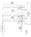
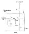
도 3은 적응적인 스위치 모드 LED 드라이버(300)의 제1 실시예의 회로 다이어그램이다. 상기 실시예는 하나 이상의 병렬 LED 채널들을 구동하는 부스트 컨버터(301)를 포함한다. 각각의 LED 채널에서, LED 스트링(302)은 LED 스트링(302)을 통하는 전류를 조절하기 위해 LDO(304)와 직렬로 연결(couple)되었다. LED 스트링(302) 및 LDO(304) 또한 둘 다 LED 스트링(302) 내의 LED들의 켜지는 순간(on-time)들 및 꺼지는 순간(off-time)들의 제어를 위해 PWM 스위치 QP(예를 들면, NMOS 트랜지스터)와 직렬로 연결(couple)되었다. 휘도 컨트롤러(310)는 제어 신호들(308)을 통해 PWM 스위치들 QP를 제어하는 것과 제어 신호들(309) 및 디지털-투-아날로그 컨버터들(digital-to-alalog converters; DACs)(307)을 통해 LDO(304)들을 제어하는 것으로써 각각의 LED 채널의 휘도 출력을 독립적으로 제어한다. 상기 LDO들(304)은 멀티플렉서(multiplexer)(311) 및 ADC(313)를 통해 휘도 컨트롤러(310)로 피드백 제어 신호(315)를 출력한다. 또한, 휘도 컨트롤러(310)는 Vboost 전압(312)을 제어하기 위해 부스트 컨버터(301)로 제어 신호(314)를 출력한다. 도 3이 단지 3개의 LED 채널들을 도시하였음에도 불구하고, LED 드라이버(300)는 임의의 개수의 LED 스트링들(302) 및 대응하는 제어/조절 회로(circuitry)를 포함할 수 있다.3 is a circuit diagram of a first embodiment of an adaptive switch
부스트Boost 컨버터 Converter
부스트 컨버트(301)는 입력 전압 Vin을 수신하고, LED 스트링들(302)로 조절된(regulated) 전력을 제공한다. 일 실시예에서, 부스트 컨버터(301)는 인덕터 L1, 다이오드 D1, 캐패시터 C1, 스위치 QB(예를 들면, NMOS 트랜지스터), 레지스터들 R1, R2 및 부스트 컨트롤러(316)를 포함한다. 부스트 컨트롤러(316)는 스위치 QB의 듀티 사이클을 제어한다. 공급 전압 Vin으로부터의 입력 전력은 스위치 QB가 켜질 때, 다이오드 D1이 역 바이어스(reverse biased)가 되므로 인덕터 L 내에 저장된다.Boost
출력 전압 Vboost는 상기 LED들을 통해 전류를 공급하도록 상기 LED들의 스트링들(302)에 인가된다. 부스트 컨트롤러(316)는 레지스터들 R1 및 R2를 포함하는 전압 디바이더(divider)를 통해 Vboost를 감지하며, Vboost를 조절하기 위해 QB의 스위칭을 제어한다. 부스트 컨트롤러(316)는 스위치 QB의 온 및 오프 상태들과 듀티 사이클들을 제어하기 위해 펄스 폭 변조(pulse-width-modulation; PWM) 또는 펄스 주파수 변조(pulse frequency modulation; PFM)와 같은 다수 개의 잘 알려진 변조(modulation) 기법들 중 임의의 하나를 채용할 수 있다. PWM 및 PFM은 출력 전력 조절(regulation)을 달성하기 위해 상기 스위치 QB를 구동하는 출력 구동 펄스(output drive pulse)의 폭들 및 주파수들을 각각 제어함에 의함으로써 상기 스위칭 전력 컨버터들을 제어하기 위해 사용되는 종래의 기법들이다. 이 피드백 루프는 부스트 컨버터(301)가 Vboost를 부스트 컨트롤러(316)에 의해 세트된 프로그램된 레벨로 유지하는 것을 허용한다.An output voltage Vboost is applied to the strings of
선형Linear드롭아웃Dropout 레귤레이터( regulator(LinearLinearDropoutDropoutRegulatorRegulator;;LDOLDO))
LDO(304)는 각각의 LED 채널을 위한 프로그램된 전류 레벨들에 따라 상기 LED 스트링들(302)을 통하는 전류를 조절한다. 각각의 LDO(304)는 연산 증폭기(operational amplifier; op-amp)(306), 감지 레지스터 RS 및 패스 트랜지스터 QL(예컨데 NMOS 트랜지스터)를 포함한다. 패스 트랜지스터 QL 및 및 감지 레지스터 RS는 PWM 스위치 QP 및 접지 단자(ground terminal) 사이에 직렬로 연결(couple)되었다. op-amp(306)의 출력은 상기 LDO(304)를 통하는 전류를 제어하기 위해 패스 트랜지스터 QL의 게이트에 연결(couple)되었다. op-amp(306)는 양 입력 신호 Vref를 DAC(307)로부터 수신하고, 패스 트랜지스터 QL의 소스(source)로부터 음 피드백 루트를 통해 음 입력 신호 Vsense를 수신한다.
LDO(304)는 Vsense를 통해 상기 LED 스트링을 통하는 전류를 감지하는 피드백 루프를 포함하며, Vref에 의해 세트된 프로그램된 전류 레벨로 상기 감지된 전류를 유지하기 위해 상기 패스 트랜지스터 QL을 제어한다. 만약, Vref가 Vsense보다 더 높다면, op-amp(306)은 패스 트랜지스터 QL에 인가되는 게이트 전압을 증가시켜, LED 스트링(302) 및 감지 레지스터(RS)를 통하는 전류 흐름을, 그것이 Vref에서 안정될 때까지 증가시킨다. 만약, Vsense가 Vref보다 높게 된다면, op-amp(306)은 패스 트랜지스터 QL에 인가되는 게이트 전압을 감소시켜, RS를 통하는 전류 흐름을 감소시키고 그것이 Vref에서 안정될 때까지 Vsense가 떨어지게 한다. 따라서, LDO(304)는 Vsense를 Vref에서 유지하기 위해 피드백 루프를 사용하고, 그렇게 함으로써 상기 LED 스트링(302)를 통하는 전류를 Vref에 비례하는 고정된 값으로 유지한다.
휘도 컨트롤러 및 제어 로직(Luminance controller and control logiclogiclogic))
휘도 컨트롤러(310)는 각각의 LED 채널의 특성들을 모니터하고, LED 채널들간의 밝기 매칭(matching)을 유지하고 전력 효율을 최적화하기 위해 상기 정점 전류들 및 PWM 듀티 사이클들을 세트한다. 휘도 컨트롤러(310)는 LDO들(304), PWM 스위치들 QP, 멀티플렉서(311) 및 부스트 컨버터(301) 각각을 제어하기 위해 제어 신호(308, 309, 318 및 314)를 출력한다. 또한, 휘도 컨트롤러(310)는 LDO들(304) 및 밝기 제어 입력(317)으로부터 피드백 신호(315)를 수신한다.The
제어 신호들(309)은 디지털로 DAC들(307)의 출력들을 세트하며, 상기 출력들은 차례로 LED 스트링들(302)을 통하는 상기 프로그램된 전류를 세트하는 상기 아날로그 참조 전압 Vref를 제공한다. 일 실시예에서, 제어 신호(309)는 8개의 가능한 프로그램가능한 전류들을 허용하는 3 비트 DAC 워드(word)이다. 예를 들어, 일 실시예에서 각각의 LED 채널은 2mA씩 증가하는 40mA부터 54mA까지의 범위 내에 있는 전류를 위해 세트될 수 있다. 휘도 컨트롤러(310)는 아래에서 설명될 것과 같은 캘리브레이션 스테이지 동안 각각의 LED 채널을 위한 상기 프로그램된 전류를 결정한다. DAC(307)의 정확도는 LED 채널들 간의 매우 좋은 매칭을 제공하기 위해 10 비트보다 좋을 수 있다. 휘도 컨트롤러들(310)은 각각의 LED 채널을 독립적으로 제어하여, 상이한 LED 채널들이 상이한 프로그램된 전류들을 위해 구성될 수 있게 한다.Control signals 309 digitally set the outputs of the
제어 신호들(308)은 LED 채널을 위한 PWM 듀티 사이클에 따라 상기 LED 채널 각각을 위한 PWM 스위치들 QP를 디지털로 제어한다. 하기에서 설명될 상기 캘리브레이션 스테이지 동안 휘도 컨트롤러(310)는 상기 프로그램된 전류의 함수로서 각각의 LED 채널을 위한 상기 PWM 듀티 사이클을 결정한다. 휘도 제어기(310)는 각각의 LED 채널의 듀티 사이클을 독립적으로 제어하여, 상이한 LED 채널들은 상이한 PWM 듀티 사이클들을 위해 구성될 수 있다. 주어진 LED 채널을 위한 상기 PWM 듀티 사이클 및 프로그램된 전류는 상기 LED 채널 내의 LED들의 밝기 출력을 총괄하여(collectively) 결정한다.Control signals 308 digitally control the PWM switches QP for each of the LED channels in accordance with the PWM duty cycle for the LED channel. During the calibration stage described below, the
제어 신호(318)는 멀티플렉서(311)의 스위칭(switching)을 제어한다. 휘도 컨트롤러(310)는 상기 멀티플렉서(311)의 선택 선(select line)(318)을 스위칭함으로써 ADC(313)을 통해 상이한 LED 채널들로부터의 피드백 신호들을 연속적으로 모니터한다. 하기에서 더 자세히 설명될 상기 캘리브레이션 스테이지 내에서, 상기 휘도 컨트롤러(310)는 멀티플렉서(311)로부터의 상기 피드백 신호(315)를 사용한다.The
제어 신호(314)는 하기에서 기술된 상기 캘리브레이션 스테이지 동안 공급 전압 Vboost를 차례로 세트하는 부스트 컨트롤러(316)를 제어한다. 제어 신호(314)는 상기 피드백 레지스터들 R1, R2의 접합부(junction)에 전류를 가함에 의한 것 또는 부스터 컨트롤러(316) 내부의 참조(reference)에 변화를 일으키는 디지털 메시지(message)를 전송함에 의한 것과 같이, 임의의 개수의 통상적인 방식들로 Voost를 세트할 수 있다.The
휘도 컨트롤러(310)는 각각의 채널 n을 위한 상대적 밝기 입력 BIn을 특정(specify) 하는 외부의(external) 밝기 입력(317)을 수신한다. 일 실시예에서, 상기 밝기 입력 BIn은 미리 정의된 최대 밝기의 백분율로서(예를 들면, BI1 = 60%, BI2 = 80%, BI3 = 100% 등) 각각의 LED 채널 n을 위한 희망되는(desired) 상대적 밝기를 표현한다. 채널의 밝기 출력은 상기 듀티 사이클에 직접적으로 비례하기 때문에 상기 휘도 컨트롤러(310)는 상기 밝기 입력 BIn을 상기 채널을 위한 기저선 듀티 사이클로서 사용한다. 따라서, 예를 들어, 60%의 밝기 입력 BIn은 (상기 최대 밝기에 대응하는) 상기 최대 듀티 사이틀의 60%의 채널 n을 위한 기저선 듀티 사이클을 가리킨다. 그러나, 상기 휘도 제어기(310)는 LED 채널들 사이의 알려진 전류 변동들을 보상하기 위한 보상 인수(factor)에 의해 PWM 스위치 QP를 구동하는 상기 듀티 사이클 신호를 생성할 때 이 기저선 듀티 사이클을 수정하고, 상기 희망되는 상대적 밝기를 유지한다. 이 보상 인수 및 상기 결과로서 나타나는 듀티 사이클 신호(308)는 하기에서 설명되는 캘리브레이션 처리(process) 동안 결정된다.The
휘도 컨트롤러Luminance controller캘리브레이션calibration 스테이지 stage
휘도 컨트롤러(310)는 각각의 LED 채널을 위한 정점 전류 및 PWM 듀티 사이클을 결정하는 작동(예를 들면, 착수(startup) 후 얼마 안 되어)의 시작 시에 캘리브레이션 스테이지에 진입한다. 각각의 LED 채널은 상기 LED 스트링들(302) 사이의 제조 변동들에 대한 보상을 위해 독립적으로 세트되고, 상기 외부 밝기 입력(317)에 의해 세트되는 LED 채널들 간의 상기 상대적 밝기 출력들을 유지한다. 따라서, 상기 휘도 컨트롤러(310)는 동일한 밝기 입력들을 갖게 구성된 채널들이 대체로(substantially) 매칭하는 밝기 출력들을 갖는다는 것을 보장한다.The
상기 캘리브레이션 스테이지의 일 실시예에서, 휘도 컨트롤러(310)는 처음에 각각의 LED 채널을 위한 DAC들(307)을 그것들의 최대 가능한 레벨들로 세트한다. 다음으로 Vboost는 상기 LED 채널들의 모두가 미리 정의된 마스터(master) 전류 레벨 Iset(예를 들면, Iset = 40 mA)에서, 또는 그보다 위에서 작동할 때까지 (제어 신호(314)를 통해) 증분적으로(incrementally) 증가된다. 다른 채널들이 상기 LED 스트링들(302)의 상이한 I-V 특성들 때문에 더 높은 전류 레벨들에서 작동하는 반면에, 상기 가장 약한 채널(즉, 상기 LED 스트링(302)를 걸치는 가장 큰 순전압 강하를 갖는 상기 LED 채널)은 Iset에서 또는 그 근처에서 작동할 것이다. 그 다음, 휘도 컨트롤러(310)는 한 순간에 하나씩 각각의 LED 채널을 캘리브레이트한다. 각각의 채널 캘리브레이션에서, 휘도 컨트롤러(310)는 멀티플렉서(311)가 상기 LED 채널을 선택하도록 구성하고, ADC(313)는 상기 선택된 LED 채널에 대한 (Vsense를 통해) 상기 전류의 샘플을 얻는다. 상기 휘도 컨트롤러(310)는 상기 DAC(307)에 의해 프로그램가능한 가장 가까운 가능한 전류 레벨(예컨대, 8개의 가능한 프로그램가능한 전류들 중 하나)로 상기 감지된 전류의 끝수를 잘라버리고(즉, 퀀타이즈(quantizes)한다.), 상기 채널 n을 위한 In으로서 상기 퀀타이즈된 전류 레벨을 저장한다. 상기 전류 In는 상기 LED 채널n이 상기 공급 전압 Vboost 하에서 유지할 수 있는 가능한 프로그램가능한 전류들의 집합으로부터의 가장 큰 전류에 대응할 것이다. 상기 캘리브레이션 처리는 상기 LED 채널들 n 각각을 위한 프로그램된 전류 레벨 In을 결정하기 위해 반복된다. 캘리브레이션 후의 일반적인(normal) 작동 동안, 각각의 LED 채널 n은 상기 결정된 프로그램된 전류 In으로 세트된다. 상기 캘리브레이션 처리는 최적의 전력 효율을 위해 각각의 LDO(304)가 LDO(304) 각각의 포화(saturation) 점의 아래, 그러나 그 근처에서 작동하는 것을 일반적으로 보장한다. 최악의 사례에서, 상기 포화 전류가 상기 최대 DAC 세팅보다 클 때, 상기 LDO(304)는 상기 LDO(304)의 트라이오드(triode) 및 포화 영역 사이의 인터페이스 점에 가능하한 가깝게 포화 상태에서 작동할 것이다.In one embodiment of the calibration stage, the
각각의 LED 채널 n을 위해 결정된 상기 프로그램된 전류 레벨 In에 기반하여, 상기 휘도 컨트롤러(310)는 하기의 수학식 1을 사용하여 각각의 LED 채널을 위한 PWM 듀티 사이클(PWM_outn)을 결정한다.Based on the programmed current level In determined for each LED channel n, the

여기서, BIn는 상기 채널 n을 위한 희망되는 상대적 밝기 세팅을 나타내는 상기 기저선 듀티 사이클이고, Iset는 상기 미리 정의된 마스터 전류 레벨이다. 수학식 1은 채널들 사이의 상기 전류 변동들을 보상하기 위해 상기 보상 인수
상기 휘도 컨트롤러(310)의 작동을 그 이상으로 예시하기 위한 예가 제공된다. 이 예에서, 상기 PWM 밝기 입력(317)은 각각의 채널 n의 상기 상대적 밝기 BIn을 60%의 밝기로 세트하고, 마스터 전류 세팅 Iset를 40mA로 설정한다. 상기에서 설명된, 상기 캘리브레이션 스테이지 동안, 상기 휘도 컨트롤러(310)는 제1 LED 채널을 I1 = 46mA의 전류 레벨로, 제2 LED 채널을 I2 = 40mA의 전류 레벨로 또한 제2 LED 채널을 I3 = 40mA의 전류 레벨로 세트하여, 각각의 LED 채널은 그것들의 포화 점들에 가까이, 그러나 그 아래에서 작동한다. 상기 휘도 컨트롤러(310)는 각각의 LED 채널을 위한 상기 듀티 사이클들 PWM_outn을 하기의 수학식 2 내지 4와 같이 결정하기 위해 수학식 1을 상기 프로그램된 전류 레벨들에게 적용한다(apply).Examples are provided to further illustrate the operation of the


따라서, 상기 캘리브레이션 처리는 각각의 LED 채널 n에 대해 전류들 In 및 듀티 사이클들 PWM_outn을 결정한다. 유익하게도, 각각의 LED 채널은 동일한 평균 전류(PWM_outn × In = 24mA)를 갖게 된다. 그러므로, 밝기 출력은 상기 LED 채널을 통하는 상기 평균 전류와 밀접히 관련되었기 때문에, 각각의 LED 채널의 관측된(observer) 밝기는 잘 매치된다.Thus, the calibration process determines currents In and duty cycles PWM_outn for each LED channel n. Advantageously, each LED channel will have the same average current (PWM_outn x In = 24 mA). Therefore, since the brightness output is closely related to the average current through the LED channel, the observed brightness of each LED channel matches well.
만약 상기 상대적 밝기 입력 BIn이 상이한 채널들 n을 위해 상이하게 세트된다면, 수학식 1은 상이한 채널들의 평균 전류들 간의 비가 상기 밝기 입력들 간의 비와 매치하는 것을 보장한다. 예를 들면 4번째 채널이 밝기 입력 BI4 = 75%를 위해 구성되었고, 및 제5 채널이 밝기 입력 BI5 = 25%를 위해 구성되었으면, 상기 휘도 컨트롤러(310)는 상기 제4 및 제5 채널 사이의 평균 전류의 비가 3:1이 되도록 채널들을 캘리브레이트한다.If the relative brightness input BIn is set differently for different channels n, then
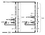
도 4a 및 4b는 도 1의 전통적인 LDO-기반 LED 드라이버(100)의 전력 손실 및 본 발명의 적응성의 스위치 모드 LED 드라이버의 차이들을 도시한다. 도 4a의 제1 LED 채널(401)에서, Vboost는 상기 LED 채널(401)을 통하는 40mA의 전류를 획득하도록 35.5 볼트로 조절되었다. LDO 트랜지스터(415)는 0.2 볼트가 강하(drop)하며 PWM 트랜지스터(413)는 0.1 볼트가 내려간다. LED 스트링(411)은 40 mA에서 35.0 볼트의 전압 강하를 갖는다. 제2 LED 채널(402)에서, 제1 LED 채널(401) 내의 LED 스트링(411) 및 제2 LED 채널(402) 내의 LED 스트링(421) 사이에서, LED 스트링(421)은 제조 차이 때문에 40 mA에서 34.0 볼트의 전압 강하를 갖는다. 전통적인 LDO 접근 방법을 사용하는 상기 제2 LED 채널 내의 상기 PWM 트랜지스터(423), LDO 트랜지스터(425) 및 감지 저항(427)에 의해 소멸된 총 전력은 60mW이다. 이 낭비된 전력은 다중-스트링 LED 드라이버 내에서 원하지 않은 열을 발생시킨다.4A and 4B illustrate the power loss of the traditional LDO-based
도 4b의 제3 LED 채널(403)은 본 발명의 적응성의 접근 방법의 이점들을 도시한다. 상기 제3 LED 채널(402) 내의 LED 스트링(432)의 특성들은 상기 제2 LED 채널(402) 내의 LED 스트링(421)과 동일하다고 가정한다. 그러나, 이 LED 채널(403)은 대신 본 발명의 적응성의 스위치 모드 LED 드라이버(300)를 사용하여 구동된다. 상기에서 설명된 상기 캘리브레이션 처리를 사용하여, 휘도 컨트롤러(310)는 상기 LDO 레귤레이터가 포화 점과 가깝게, 그러나 그 아래에서(near but below) 작동하도록 상기 제3 LEF 채널(403) 내의 전류를 48 mA로 세트할 것이다. 상기 증가된 전류에 비례하는 LDO 트랜지스터(435), PWM 트랜지스터(423) 및 감지 저항(427)를 관통하는(across) 증가된 전압 강하가 있다. 수학식 1을 적용하면, 상기 PWM 듀티 사이클은 83%로 조절된다. 본 발명의 적응형의 접근 방법을 사용하면, PWM 트랜지스터(423), LDO 트랜지스터(435) 및 감지 저항(427)에 의한 소멸된 총 전력은 단지 28.8.mW이다. 따라서, LED 드라이버(300)는 상기 전통적인 LDO 드라이버(100)에 비해 전력 효율에 있어 대폭적인(substantial) 향상을 제공한다. 또한 LED 드라이버(300)는 상기에서 참조된 유휘 챈(Yuhui Chen) 등에 의한 미국 특허 출원 12/164,909번 내에 설명된 완전 디지털 스위치 접근 방법에 대한(over) 이점들을 제공한다. 이는 휘도 컨트롤러(310)가 가능한 채널 전류들의 단지 제한된 범위만을 허용하기 때문이다. 이는 LED 채널들 사이의 전류들의 넓고 동적인 범위로 인해 야기되는 구성 요소 스트레스 및 신뢰성에 관한 문제를 제거한다.The
LDOLDO 드라이버의 대안적인 Driver Alternative실시예Example
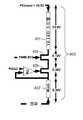
도 5는 적응상의 스위치 모드 LED 드라이버(500)의 제2 실시예를 도시한다. 상기에서 설명된 LED 드라이버(500)는 도 3의 LED 드라이버(300)와 유사하나, 변형된(modified) LDO(504)를 구비하고 ADC(313)이 없다. LDO(504)는 상기에서 설명된 LDO(304)의 구성과 유사하게, op-amp(306), 패스 트랜지스터 QL 및 감지 저항(RS)를 LDO 구성(configuration) 내에 포함한다. 그러나, LDO(504)는 추가적으로 op-amp(306)의 출력(551)을 참조 전압(553)과 비교하는 비교기(506)를 포함하고, 결과로서 나타나는 신호를 상기 멀티플렉서(311)로 출력한다. 다른 대안적인 실시예들에서, 비교기(506)로의 입력(551)은 op-amp(306)의 입력 대신에, LDO 트랜지스터 QL의 드레인 또는 소스로 연결(couple)될 수 있다.5 shows a second embodiment of an adaptive switch
도 5의 실시예에서, 휘도 컨트롤러(310)는 각각의 채널에 대한 상기 프로그램된 전류 IN 및 듀티 사이클 PWM_outn을 결정하기 위한 변형된 캘리브레이션 처리를 가한다(apply). 상기 캘리브레이션 스테이지 동안, DAC들(307)은 그것들의 가장 낮은 레벨로 모두 초기화된다. 다음으로 Vboost는 제어 신호(314)에 의해 상기 LED 채널들 모두가 상기 요구되는 Iset 레벨에서 또는 그 위에서 작동할 때까지 증분적으로 증가된다. 일단 Vboost가 적당한 레벨에 도달하면, 휘도 컨트롤러(310)는 각각의 LED 채널을 위한 DAC들(307)을 그것들의 가장 낮은 레벨에서부터 그것들의 가장 높은 레벨까지 차례로 나열하고(sequence), 멀티플렉서(311)를 통해 비교기들(506)로부터의 출력들을 모니터한다. 상기 DAC 출력이 LDO(504)가 상기 프로그램된 레벨에서의 전류를 유지하기에는 너무 높게 되었을 때, 비교기(506)의 출력은 경사져서 올라가고(ramp up) 임계 전압(533)을 초과한다. 휘도 컨트롤러(310)는 상기 임계 전압(553)이 상기 LED 채널 n을 위한 상기 전류 레벨 In으로서 초과되기 전에 각각의 LED 채널을 위한 상기 가장 높은 가능한 DAC 세팅을 저장한다.In the embodiment of FIG. 5, the
도 5의 실시예는 각각의 LDO(504)가 깊은(deep) 포화로 가지 않고(without going into) 상기 트라이오드 및 포화 영역들 사이의 인터페이스 점에 가능하한 가깝게 작동하는 것을 보장하는 이점을 갖는다. 이는 정확한 조절을 유지하는 반면에 각각의 LDO(504) 내의 최소한의 전력 소멸을 보장한다. 하기의 캘리브레이션에서, LED 드라이버는 도 3의 LED 드라이버(300)과 동일하게 작동한다.The embodiment of FIG. 5 has the advantage of ensuring that each
휘도 이동 함수 보상Luminance Shift Function Compensation
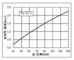
대안적인 실시예에서, 휘도 컨트롤러(310)는, 상기 LED들의 광속 및 순전류(forward current) 간의 관계에서의 비-선형성(non-linearity)을 참작하기 위해(account for) 수학식 1의 변형된 버전을 가한다. 도 6은 전류의 함수로서, 순방향 전도(forward conducting) LED로부터 발해지는 상대적 광속의 그래프이다. 상기 그래프는 순 전류가 증가함에 따른 광학 효율 강하를 도시하며, 이는 경사도에서 약간의 감소를 일으킨다. 일 실시예에서, 휘도 컨트롤러(310)는 하기의 수학식 5의 형태의 2차 다항식을 사용하여 상기 휘도 이동 함수의 모델을 만든다.In an alternative embodiment, the

여기서 상기 C0, C1 및C2는 실험적으로 결정된 상수이다. 이 실시예에서, 휘도 컨트롤러(310)는 각각의 LED 채널 n을 위한 PWM_outn을 결정하기 위해 하기의 보상 등식(equation)을 가한다.Wherein C0 , C1 and C2 are constants determined experimentally. In this embodiment, the

LED 채널 사이의 평균 전류들의 비를 상기 밝기 입력들 BIn의 비로 매치시키는 상기 수학식 1에 대비하여, 수학식 6은 대신 상기 상대적 밝기 BIn에 비례하도록 LED 채널의 상대적 광속 출력을 세트한다. 따라서, 동일한 밝기 입력들로 구성된 LED 채널들은 대체로 같은 밝기 출력을 가질 것이다.In contrast to
일 실시예에서, 광속 컨트롤러(310)는 상기 캘리브레이션 스테이지 동안 각각의 LED 채널 n을 위한 비
온도 보상Temperature compensation
또 다른 대안적인 실시예에서, 휘도 컨트롤러(310)은 상기 LED 채널들 간의 온도 변동들에 대한 보상을 부가적으로 제공하는 수학식 1의 상이한 변형된 버전을 적용할 수 있다. 도 7은 접합부 온도의(junction temperature) 함수로서 55 mA의 순전류를 가진 상대적인 순방향 바이어스된(forward biased) LED로부터 발해지는 광속 밀도 그래프이다. 상기 그래프는 섭씨(centigrade) 25도에서 85도로 상기 LED들의 접합부 온도가 상승됨에 따라, 휘도 상의 약 12% 감소를 도시한다. 이 감소는 대체로 온도의 선형 함수이다. 따라서, 일 실시예에서 휘도 컨트롤러(310)는 각각의 LED 채널 n을 위한 PWM_outn을 결정하기 위해 하기의 수학식 7을 적용한다.In another alternative embodiment, the

여기서 CT는 실험적으로 결정된 온도의 선형 함수이다. 이 실시예에서, 휘도 컨트롤러(310)는 휘도 컨트롤러(310)로 온도 데이터를 제공하기 위해 구성된 추가적인 온도 입력 신호(도시되지 않음)을 포함하기 위해 변형되었다. 상기 온도 데이터는 임의의 종래의 LED 온도 측정 기법들을 사용하여 획득될 수 있다.Where CT is a linear function of the temperature determined experimentally. In this embodiment, the
샘플 및 홀드 회로Sample and Hold Circuit
도 8은 샘플 및 홀드 특색(feature)을 포함하는 LDO(801)의 실시예를 도시하는 회로 다이어그램이다. 명확성 및 편의를 위해, 상기 샘플 및 홀드 LDO(801)는 LDO(304)의 변형된 버전으로서 도시되었고, 도 3의 LDO 드라이버(300)와 호환성이 있다. 그러나, 도 5의 LDO(504)는 하기에서 설명된 LDO(801)의 샘플 및 홀드 특색들을 포함하기 위해 또한 변형될 수 있다. 따라서, 상기 샘플 및 홀드 특색들은 도 5의 LDO 드라이버(500)와 또한 호환성이 있다.8 is a circuit diagram illustrating an embodiment of an LDO 801 that includes sample and hold features. For clarity and convenience, the sample and hold LDO 801 is shown as a modified version of the
샘플 및 홀드 LDO(801)는 상기에서 설명된 LDO(304)의 모든 구성 요소들을 포함하나, 추가적으로 캐패시터(capacitor)들(809, 811) 및 스위치들(808, 810)을 포함한다. 샘플/홀드 스위치(808) 및 캐패시터(809)를 포함하는 제1 샘플 및 홀드 구성 요소는 op-amp(306)의 출력 및 트랜지스터 QL의 게이트 사이에 연결(couple)되었다. 샘플/홀드 스위치(810) 및 캐패시터(811)를 포함하는 제2 샘플 및 홀드 구성 요소는 감지 저항 RS 및 op-amp(306)의 입력 사이의 상기 음 피드백 경로 내에 연결(couple)되었다. 이 샘플 및 홀드 특색은 LDO(801)가 상기 PWM 제어 트랜지스터 QP가 꺼질때 마다 그것의 전류가 인터럽트(interrupt)됨에도 불구하고 계속하여 작동하도록 허용한다. 스위치들(808, 810)은 휘도 컨트롤러(310)로부터의 추가적인 제어 신호들(도시되지 않음)을 통해 디지털로 제어된다.The sample and hold LDO 801 includes all the components of the
작동 중에, 휘도 컨트롤러(310)는 PWM 스위치 QP가 꺼지기 직전에 스위치들(808, 810)을 연다(open). 캐패시터들(809, 811)은 트랜지스터 QL의 게이트-소스 전압 및 PWM 스위치 QP의 꺼진 시간(off-time)을 위한 일정한(constant) 레벨들에서 상기 연산 증폭기(306)의 음 입력에서의 전압을 유지한다. 스위치들(808, 810) 및 캐패시터들(809, 811)은 유익하게도 PWM 스위치 QP가 오프일 때마다 op-amp(306)의 출력을 Vdd 레일(rail)에 가깝게 하도록 LDO 트랜지스터 QL의 게이트를 구동하는 것으로부터 방지한다. 이는 PWM 스위치 QP가 켜질 때 op-amp(306)가 이미 바른 값, 또는 그 근처에 있는 것을 보장함으로써 모든 PWM 사이클의 리딩 에지(leading edge)에서 상기 LED 스트링들(302)을 통하는 전류 스파이크(spike)들을 방지한다. PWM 스위치 QP가 다시 켜진 직후, 휘도 컨트롤러(310)는 스위치들(808, 810)을 닫고, 연속적인 시간 선형 조절(regulation)을 재개한다. 상기 샘플 및 홀드 특색은 LDO(801)이 매우 빠른 동적 응답을 가지고 극심한 듀티 사이클들에 걸쳐 작동하는 것을 허용한다.In operation, the
결함 감지 회로Fault detection circuit
도 9는 LED 드라이버(300) 또는 LED 드라이버(500)와 같이 사용하기 위한 결함 감지 회로의 일 실시예를 도시한다. 도 9가 LDO(504)의 문맥 내에서의 상기 결함 감지 회로를 도시하였음에도 불구하고, 상기 결함 감지 회로의 특색은 상기에서 설명된 LDO(304)를 사용하는 실시예들에서나 샘플 및 홀드 LDO(801)에서도 또한 포함될 수 있다.9 illustrates one embodiment of a fault detection circuit for use with
상기 결함 감지 회로는 저항 RESD, 전류 소스들(912, 915), 스위치들(913, 914) 및 비교기(920, 921)를 포함한다. 전류 소스(912), 스위치(913) 및 저항 RESD는 아날로그 전압 소스 Vdda 및, 예컨대 PWM 트랜지스터 QP의 드레인 핀(926)과 같은 시험 점(test point) 사이에 모두 직렬로 연결(couple)되어 있다. 전류 소스(915), 스위치(913) 및 저항 RESD는 상기 핀(926) 및 접지 단자 사이에 모두 직렬로 연결(couple)되어 있다. 비교기들(920, 921)은 저항 RESD를 통해 드레인 핀(926)에서의 전압을 감지하고, 상기 전압을 오픈 임계치 전압(open threshold voltage)(918) 및 단락 임계치 전압(close threshold voltage)(919)에 각각 비교한다. 이 실시예에서, 휘도 컨트롤러(310)는 상기 결함 감지 특색들을 수행하기 위한 추가적인 입력들 및 출력들(916, 917, 922, 923)(도 3 및 도 4 내에 도시되지 않음)을 포함한다. 상기 결함 감지 회로는 세 종류의 결함들을 감지한다: (1) 상기 PWM 트랜지스터 QP의 드레인 핀(926)에서의 "짧은 타입" 결함들; (2) 상기 LED 스트링(302) 내에서의 "오픈(open) 타입" 결함들; 및 (3) 상기 LED 스트링(302) 내에서의 "LED 짧은 타입" 결함들. 결함 방지(protection)의 각각의 타입의 작동들은 하기에서 설명된다.The fault detection circuit includes a resistor RESD ,
짧은 타입 결함들은 대체적으로 전력 공급(power up) 일련(sequence) 동안 수행되는 "단락 감지" 시험 동안 감지된다. 상기 핀 단락 시험 동안, 휘도 제어기(310)는 페이즈 1 제어 신호(916)를 통해 스위치(913)를 켜고(즉, 닫고), LDO 트랜지스터 QL 및 PWM 트랜지스터 QP를 끈다. 전류 소스(912)는 저항 RESD를 통해 드레인 핀(926)으로 적은 전류(예를 들면, 약 100 μA)를 공급하는 것을 시도한다. 만약, 핀(926) 상의 접지(ground)로의 단락이 있다면, 핀(926)에서의 전압은 거의 0 볼트에 가깝게 떨어질 것이다. 그렇지 않으면, 상기 전압은 아날로그 공급 레일 전압 Vdda에 가깝게 올라갈 것이다. 핀(926)은 저항 RESD를 통해 모니터되고, 비교기(921)에 의해 단락 임계치 전압(919)과 비교된다. 만약, 모니터된 전압이 단락 임계치 전압(919)보다 낮다면, 상기 LED 채널은 상기 핀(926)으로부터 접지로의 단락을 갖는다. 단락은 단락 감지 신호(923)에 의해 가리켜진다. 일 실시예에서, 단락이 감지되었을 때, 상기 LED 채널의 더 이상의 작동은 가능하지 않게 된다. 상기 핀 단락 시험의 마지막에, 페이즈 1 제어 신호(916)은 스위치(913)를 끄고(즉, 열고), 그것은 일반적인 동작 동안 꺼진 채 남는다.Short type faults are typically detected during a "short detect" test performed during a power up sequence. During the pin short test,
오픈(open) 타입 결함들은 역시 전력 공급(power up) 일련(sequence) 동안 수행되는 "오픈 감지" 시험 동안 감지된다. 휘도 제어기(310)는 페이즈 2 제어 신호(917)를 통해 스위치(913)를 켠다(즉, 닫는다). 전류 소스(915)는 저항 RESD를 통해 핀(926)으로부터 적은 전류(예를 들면, 약 100 μA)를 끌어내는(draw) 것을 시도한다. 만약, LED 스트링(302)이 핀(926)으로 제대로 연결되어 있지 않으면, 핀(926)에서의 전압은 거의 0 볼트에 가깝게 떨어질 것이다. 핀(926)에서의 전압은 저항 RESD를 통해 모니터되고, 비교기(920)에 의해 오픈 단락 임계치 전압(918)과 비교된다. 만약, 모니터된 전압이 오픈 임계치 전압(918)보다 아래로 떨어진다면, 상기 휘도 컨트롤러(310)는 상기 LED 채널이 상기 핀(926)으로부터 LED 스트링(302)으로의 열린 경로(open path)를 가졌는지를 결정한다. 상기 열린 경로는 오픈 감지 신호(922)에 의해 가리켜진다. 일 실시예에서, 오픈 타입 결함이 감지되었을 때, 상기 LED 채널의 더 이상의 작동은 가능하지 않게 된다. 상기 시험의 마지막에, 스위치(914)는 페이즈 2 제어 신호(917)에 의해 꺼지고, 그것은 일반적인 동작 동안 꺼진 채 남는다.Open type faults are detected during an "open sense" test, which is also performed during a power up sequence. The
LED 단락 타입의 결함들은 일반적인 동작 동안 주기적으로 수행된다. 이 테스트는 상기 LED 채널 캘리브레이션 스테이지 동안에도 또한 사용되는 비교기(506)을 이용한다. 비교기(506)는 상기 op-amp(306)의 출력을 모니터한다. 만약 LED 스트링(302) 내의 하나 이상의 LED들이 접지로 단락되었다면, LED 스트링(302)의 순전압 강하(forward voltage drop)는 감소하고, 상기 LED채널 내의 전류는 올라가기 시작할 것이다. 상기 전류가 올라감에 따라, Vsense는 증가하고, op-amp(306)의 출력(551)은 강하한다. 출력(551)이 임계치 전압(553) 아래로 떨어질 때, 비교기(506)은 상태를 변경하고, LDO(504)가 그것의 조절(regulation) 전력 제한들을 초과하였음을 가리킨다. 이는 휘도 컨트롤러(310)에게 LED 단락 타입 실패(failure)가 발생하였음을 가리킨다. 다음으로 상기 실패한 LED 채널의 작동은 가능하지 않게 될 수 있다.LED short circuit type faults are performed periodically during normal operation. This test uses a
제조 변동 보상(Manufacturing variation compensation (manufacturingmanufacturingvariationvariationcompensationcompensation))
본 발명의 실시예들은 실리콘 공정(처리) 동안 제조 변동에 대한 보상을 포함한다. 예를 들어, 일 실시예에서 LED PWM 스위치 QP의 온 저항(on resistance; Rdson)은 전형적인 프로세스 코너(process corner)에서 5V 게이트 드라이버와 함께 5 옴의 설계 타겟(design target)을 갖는다. 상기 스위치 QP의 실제적인(actual) Rdson 저항은 자동화 시험 장비(Automatic Testing Equipment; ATE) 시험 스테이지 동안 측정될 수 있다. 일 실시예에서, 실제적인 Rdson 저항은 LED 드라이버(300) 내의 메모리(예를 들면, 휘도 컨트롤러(310)의 내)에 저장되어, 상기 휘도 컨트롤러(310)는 상기 값을 상기 LED 스트링들을 구동하는데에 사용할 수 있다. 만약 상기 스위치 QP를 위한 실리콘이 느린 프로세스 코너(slow process corner) 내에 있다면, 이 측정된 저항은 타겟된 설계 값보다 더 높을 것이고, 이는 더 높은 열 손실(thermal loss)을 결과로서 낳는다. 이 경우에서, 정상적으로는 일반적인 프로세스 코너를 위해 5 볼트로 세트될 상기 게이트 드라이버 전력 공급은, 5 옴의 동일한 타겟 저항을 유지하기 위해 더 높은 전압(예를 들면, 6V)로 대신 잘린다(trmmed). 동일한 원리가 3.3V 게이트 드라이버 회로 전력 공급들 또는 다른 타입의 게이트 드라이버들에게 또한 적용될 수 있다.Embodiments of the present invention include compensation for manufacturing variations during silicon processing (treatment). For example, in one embodiment the on resistance (Rdson) of the LED PWM switch QP has a 5 ohm design target with a 5V gate driver at a typical process corner. The actual Rdson resistance of the switch QP can be measured during the Automatic Testing Equipment (ATE) test stage. In one embodiment, the actual Rdson resistor is stored in a memory in LED driver 300 (eg, in luminance controller 310) such that
만약 상기 실리콘이 빠른 프로세스 코너(fast process corner) 내에 있다면, 상기 측정된 저항은 타겟된 설계 값보다 낮을 것이다. 상기 게이트 드라이버 전력 공급은 5 옴의 타겟 저항을 유지하기 위해 더 낮은 전압(예를 들면, 4V)로 잘려질 수 있음에도 불구하고, 상기 게이트 드라이버 전력 공급을 감소시키는데에 명백한(obvious) 이익이 없다. 그러므로, 일 실시예에서, 상기 조절은 단지 느린 프로세스 코너에서만 일어나고, 빠른 프로세스 코너에서는 일어나지 않는다.If the silicon is within a fast process corner, the measured resistance will be lower than the targeted design value. Although the gate driver power supply may be cut to a lower voltage (eg 4V) to maintain a 5 ohm target resistance, there is no obvious benefit in reducing the gate driver power supply. Therefore, in one embodiment, the adjustment only occurs at the slow process corner and not at the fast process corner.
개시된 방법은 전통적인 설계 방법론에 비교하였을 때 유리하게도 중요한(significant) 실리콘 영역(area)을 아낀다(save). 전통적인 디자인 방법론은 모든 프로세스 코너들을 포함(cover)하기에 충분한 트랜지스터들의 w/l 비(ratio)를 적게 잡게끔(conservatively) 선택한다. 상기에서 설명된 것과 같이 상기 측정된 온-저항에 기반하여 상기 게이트 드라이브 신호를 캘리브레이팅함에 의해, 덜 적게 잡은(conservative) w/l 비가 구현될 수 있고, 따라서 실리콘 영역 및 비용을 절약한다.The disclosed method advantageously saves significant silicon areas when compared to traditional design methodologies. Traditional design methodology chooses to conserve less w / l ratio of transistors sufficient to cover all process corners. By calibrating the gate drive signal based on the measured on-resistance as described above, a less conservative w / l ratio can be realized, thus saving silicon area and cost.
이 개시를 읽음에 있어, 본 기술 분야의 숙련된 이들은 상기 적응성의 스위치 모드 LED 드라이버를 위한 추가적인 대안적인 설계들 또한 이해할 것이다. 따라서, 본 발명의 특정 실시예 및 응용들이 도시 및 설명되었음에도, 본 발명은 본 문서에서 개시된 정확한 구성 및 구성 요소들로 제한되지 않는다는 것과, 본 기술 분야의 숙련된 이들에게 분명할 것인 다양한 변형(modification)들, 변경(change)들 및 변화(variation)들이 본 문서에서 개시된 본 발명의 방법 및 장치(apparatus)의 배치(arrangement), 작동(operation) 및 세부사항(detail)들 내에 상기 첨부된 청구항들 내에서 정의된 본 발명의 참뜻(spirit) 및 범위로부터 유리(depart)되지 않은 채 만들어질 수 있다는 것이 이해될 것이다.In reading this disclosure, those skilled in the art will also understand additional alternative designs for the adaptive switch mode LED driver. Thus, although specific embodiments and applications of the invention have been shown and described, it is to be understood that the invention is not limited to the precise configuration and components disclosed herein, and that various modifications will be apparent to those skilled in the art. Modifications, changes and variations are described in the appended claims within the arrangement, operation and details of the method and apparatus of the invention disclosed herein. It will be understood that they may be made without departing from the spirit and scope of the invention as defined within the scope of the invention.
Claims (27)
Translated fromKorean입력 전압을 수신하고 제1 LED 스트링으로 인가되는 출력 전압을 생성하도록 구성된 전력 컨버터;
제1 채널 스위치에 인가되는 제1 듀티 사이클 신호에 따라 상기 제1 LED 스트링을 온 또는 오프로 스위치하도록 구성된 제1 채널 스위치;
제1 프로그램된 전류 레벨 신호를 수신하고, 상기 제1 프로그램된 전류 레벨 신호에 따라 상기 제1 LED 스트링을 통하는 전류를 조절하도록 구성된 제1 채널 레귤레이터; 및
프로그램가능한 전류 레벨들의 제한된 집합 중 하나에 대응하여 상기 제1 LED 스트링을 위한 상기 제1 프로그램된 전류 레벨 신호를 생성하고, 상기 제1 프로그램된 전류 레벨 신호의 함수로서 상기 제1 채널 스위치를 구동하기 위한 상기 제1 듀티 사이클 신호를 생성하도록 구성된 휘도 컨트롤러를 포함하는 것을 특징으로 하는 LED 드라이버.An LED driver for driving one or more light-emitting diode strings, the LED driver comprising:
A power converter configured to receive an input voltage and generate an output voltage applied to the first LED string;
A first channel switch configured to switch the first LED string on or off in accordance with a first duty cycle signal applied to the first channel switch;
A first channel regulator configured to receive a first programmed current level signal and to adjust a current through the first LED string in accordance with the first programmed current level signal; And
Generating the first programmed current level signal for the first LED string in response to one of a limited set of programmable current levels and driving the first channel switch as a function of the first programmed current level signal. And a brightness controller configured to generate the first duty cycle signal for the mobile device.
상기 제1 채널 스위치는 상기 제1 LED 스트링과 직렬로 연결된 것을 특징으로 하는 LED 드라이버.In the LED driver of claim 1,
And the first channel switch is connected in series with the first LED string.
상기 제1 채널 스위치는 상기 제1 채널 레귤레이터 및 상기 제1 LED 스트링 간에 직렬로 연결된 것을 특징으로 하는 LED 드라이버.In the LED driver of claim 1,
And the first channel switch is connected in series between the first channel regulator and the first LED string.
상기 제1 휘도 컨트롤러는 상기 제1 LED 스트링에 인가되는 상기 출력 전압 하에서 상기 프로그램가능한 전류 레벨들의 제한된 집합 중 상기 제1 LED 스트링을 통하는 상기 전류가 상기 제1 채널 레귤레이터에 의해 조절될 수 있는 가장 높은 것으로 상기 제1 프로그램된 전류 레벨을 생성하는 것을 특징으로 하는 LED 드라이버.In the LED driver of claim 1,
The first brightness controller is the highest that the current through the first LED string of the limited set of programmable current levels under the output voltage applied to the first LED string can be regulated by the first channel regulator. Generate the first programmed current level.
기준치 전류 레벨에 대한 상기 제1 프로그램된 전류 레벨 신호의 비율을 결정하는 것; 및
상기 비율에 기준치 듀티 사이클을 곱하는 것을 포함하는 것을 특징으로 하는 LED 드라이버.The LED driver of claim 1, wherein the generating of the first duty cycle signal comprises:
Determining a ratio of the first programmed current level signal to a reference current level; And
Multiplying the ratio by a reference duty cycle.
제2 채널 스위치에 인가된 제2 듀티 사이클 신호에 따라 제2 LED 스트링을 온 또는 오프로 스위치하도록 구성된 제2 채널 스위치, 상기 제2 LED 스트링은 상기 제1 LED 스트링에 대해 상이한 전류-전압 특성들을 갖고; 및
상기 휘도 컨트롤러로부터 제2 프로그램된 전류 레벨 신호를 수신하고, 상기 제2 프로그램된 전류 레벨 신호에 따라 상기 제2 LED 스트링을 통하는 전류를 조절하도록 구성된 제2 채널 레귤레이터를 더 포함하고,
상기 제1 및 제2 프로그램된 전류 레벨 신호들은 상이한 프로그램된 전류 레벨들에 대응하고,
상기 휘도 컨트롤러는 상기 프로그램가능한 전류 레벨들의 제한된 집합 중 다른 하나에 대응하도록 상기 제2 LED 스트링을 위한 상기 제2 프로그램된 전류 레벨 신호를 생성하고, 상기 제2 프로그램된 전류 레벨 신호의 함수로서 상기 제2 채널 스위치를 구동하기 위한 상기 제2 듀티 사이클 신호를 결정하도록 더 구성된 것을 특징으로 하는 LED 드라이버.In the LED driver of claim 1,
A second channel switch configured to switch the second LED string on or off in accordance with a second duty cycle signal applied to the second channel switch, wherein the second LED string has different current-voltage characteristics for the first LED string; Have; And
A second channel regulator configured to receive a second programmed current level signal from the brightness controller and adjust a current through the second LED string in accordance with the second programmed current level signal;
The first and second programmed current level signals correspond to different programmed current levels,
The brightness controller generates the second programmed current level signal for the second LED string to correspond to another one of the limited set of programmable current levels, and wherein the first controller is a function of the second programmed current level signal. And determine the second duty cycle signal for driving a two channel switch.
상기 제1 및 제2 LED 스트링들은 상이한 프로그램된 전류 레벨들 및 상이한 듀티 사이클들에 따라 온 또는 오프로 스위치되나, 실질적으로 동일한 평균 전류 레벨들을 갖는 것을 특징으로 하는 LED 드라이버.In the LED driver of claim 6,
Wherein the first and second LED strings are switched on or off according to different programmed current levels and different duty cycles, but having substantially the same average current levels.
상기 제1 LED 스트링 및 상기 제1 채널 스위치와 직렬로 연결된 패스 트랜지스터; 및
상기 제1 LED 스트링을 통하는 상기 전류를 감지하고, 상기 감지된 전류를 아날로그 전류 참조와 비교하고, 상기 아날로그 전류 참조를 초과하는 상기 감지된 전류에 반응하여 상기 감지된 전류를 감소시키기 위해 상기 패스 트랜지스터를 제어하도록 구성된 피드백 루프를 포함하는 것을 특징으로 하는 LED 드라이버.The LED driver of claim 1, wherein the first channel regulator comprises:
A pass transistor connected in series with the first LED string and the first channel switch; And
The pass transistor to sense the current through the first LED string, compare the sensed current with an analog current reference, and reduce the sensed current in response to the sensed current exceeding the analog current reference. LED driver comprising a feedback loop configured to control.
상기 패스 트랜지스터의 소스에 직렬로 연결된 감지 저항기; 및
상기 패스 트랜지스터의 상기 소스에 연결된 음 입력 단자, 상기 아날로그 전류 참조를 수신하기 위해 연결된 양 입력 단자 및 상기 패스 트랜지스터의 게이트에 연결된 출력 단자를 구비한 연산 증폭기를 포함하는 것을 특징으로 하는 LED 드라이버.The LED driver of claim 8, wherein the feedback loop comprises:
A sense resistor coupled in series with the source of the pass transistor; And
And an operational amplifier having a negative input terminal coupled to the source of the pass transistor, a positive input terminal coupled to receive the analog current reference, and an output terminal coupled to the gate of the pass transistor.
상기 감지된 전류가 상기 프로그램된 전류 레벨 신호를 초과하는 때를 감지하기 위해 상기 연산 증폭기의 출력을 참조 전압과 비교하고, 비교 신호를 상기 휘도 컨트롤러로 출력하도록 구성된 비교기를 더 포함하는 것을 특징으로 하는 LED 드라이버.In the LED driver of claim 9,
And a comparator configured to compare the output of the operational amplifier with a reference voltage to detect when the sensed current exceeds the programmed current level signal and to output a comparison signal to the luminance controller. LED driver.
상기 휘도 컨트롤러는 캘리브레이션 후의 상기 LED 드라이버의 정상적인 작동 동안 상기 감지된 전류가 상기 프로그램된 전류 레벨 신호를 초과하는 것을 가리키는 상기 비교 신호에 반응하여 상기 제1 LED 스트링 내의 LED가 접지로 단락되었는지를 결정하는 것을 특징으로 하는 LED 드라이버.In the LED driver of claim 10,
The luminance controller determines whether the LED in the first LED string is shorted to ground in response to the comparison signal indicating that the sensed current exceeds the programmed current level signal during normal operation of the LED driver after calibration. LED driver, characterized in that.
상기 샘플 및 홀드 레귤레이터는,
상기 제1 채널 스위치가 오프되기에 앞서 상기 연산 증폭기의 출력 전압을 샘플링하는 것 및 상기 제1 채널 스위치가 다시 온으로 되돌아올 때까지 상기 출력 전압을 홀드하는 것을 위한 제1 샘플 및 홀드 구성요소; 및
상기 제1 채널 스위치가 오프되기에 앞서 상기 연산 증폭기의 음 입력 단자 전압을 샘플링하는 것 및 상기 제1 채널 스위치가 다시 온으로 되돌아올 때까지 상기 샘플된 음 입력 단자 전입을 홀드하는 것을 위한 제2 샘플 및 홀드 구성요소를 포함하는 것을 특징으로 하는 LED 드라이버.10. The LED driver of claim 9, wherein the first channel regulator comprises a sample and hold regulator,
The sample and hold regulator,
A first sample and hold component for sampling the output voltage of the operational amplifier before the first channel switch is turned off and for holding the output voltage until the first channel switch is turned back on; And
A second for sampling the negative input terminal voltage of the operational amplifier prior to the first channel switch being turned off and for holding the sampled negative input terminal input until the first channel switch is back on; LED driver comprising a sample and hold component.
상기 휘도 컨트롤러로부터 상기 프로그램된 전류 레벨 신호를 디지털 형태로 수신하고 상기 제1 채널 레귤레이터로 상기 아날로그 전류 참조를 출력하도록 구성된 디지털-투-아날로그 컨버터(digital-to-analog converter; DAC)를 더 포함하는 것을 특징으로 하는 LED 드라이버.In the LED driver of claim 8,
And further comprising a digital-to-analog converter (DAC) configured to receive the programmed current level signal from the luminance controller in digital form and output the analog current reference to the first channel regulator. LED driver, characterized in that.
상기 제1 채널 레귤레이터로부터 상기 휘도 컨트롤러로 상기 제1 채널 레귤레이터를 통하는 감지된 전류에 상당하는 피드백 신호를 전송하는 피드백 경로를 더 포함하고, 상기 휘도 컨트롤러는 상기 피드백 신호에 부분적으로 기반하여 상기 제1 프로그램된 전류 레벨 신호를 생성하는 것을 특징으로 하는 LED 드라이버.In the LED driver of claim 1,
A feedback path for transmitting a feedback signal corresponding to the sensed current through the first channel regulator from the first channel regulator to the luminance controller, wherein the luminance controller is based in part on the feedback signal; LED driver for generating a programmed current level signal.
상기 휘도 컨트롤러는 상기 제1 프로그램된 전류 레벨 신호의 함수로서 상기 제1 듀티 사이클 신호를 생성하여, 동일한 상대적 밝기를 위해 구성된 하나 이상의 상기 LED 스트링들 각각의 사이에서 평균 전류는 실질적으로 매치되는 것을 특징으로 하는 LED 드라이버.In the LED driver of claim 1,
The luminance controller generates the first duty cycle signal as a function of the first programmed current level signal such that an average current is substantially matched between each of the one or more of the LED strings configured for the same relative brightness. LED driver.
동일한 상대적 밝기를 위해 구성된 상기 LED 스트링들 중 적어도 몇몇 사이에서 광속이 실질적으로 매치되도록 상기 휘도 컨트롤러는 휘도 이동 함수에 부분적으로 기반하여 상기 제1 프로그램된 전류 레벨 신호의 함수로서 상기 제1 듀티 사이클 신호를 결정하는 것을 특징으로 하는 LED 드라이버.In the LED driver of claim 1,
The luminance controller allows the first duty cycle signal to function as a function of the first programmed current level signal based in part on a luminance shift function such that luminous flux substantially matches between at least some of the LED strings configured for equal relative brightness. LED driver, characterized in that for determining.
상기 휘도 컨트롤러는 온도 측정치를 수신하는 온도 입력부를 더 포함하고, 상기 휘도 이동 함수는 하나 이상의 상기 LED 스트링들 사이에서의 온도 차이들에 대한 보상을 위한 온도 보상 함수를 포함하는 것을 특징으로 하는 LED 드라이버.In the LED driver of claim 16,
The luminance controller further comprises a temperature input for receiving a temperature measurement, wherein the luminance shift function comprises a temperature compensation function for compensating for temperature differences between one or more of the LED strings. .
하나 이상의 상기 LED 스트링들 내에서 개 회로 및 단락 중 적어도 하나를 감지하는 것과 상기 개 회로 또는 상기 단락을 감지하는 것에 반응하여 상기 제1 LED 스트링을 불능화하기 위해 상기 제1 채널 스위치를 오프로 하는 것을 위한 결함 감지 회로를 더 포함하는 것을 특징으로 하는 LED 드라이버.In the LED driver of claim 1,
Sensing at least one of a short circuit and a short in the one or more LED strings and turning off the first channel switch to disable the first LED string in response to detecting the open circuit or the short. LED driver, characterized in that it further comprises a fault detection circuit.
단락 감지 시험 동안 상기 제1 채널 레귤레이터로 제1 시험 전류를 공급하는 제1 전류 소스;
상기 제1 채널 레귤레이터의 시험 점 전압을 단락 임계 전압과 비교하는 제1 비교기, 상기 비교기는 상기 단락 임계 전압을 초과하는 상기 시험 전압에 반응하여 상기 단락을 표시하고;
개 회로 감지 시험 동안 상기 제1 채널 레귤레이터로부터 제2 시험 전류를 끌어내는 제2 전류 소스; 및
상기 시험 점 전압을 개 회로 임계 전압과 비교하는 제2 비교기를 포함하고, 상기 제2 비교기는 상기 개 회로 임계 전압 아래로 떨어지는 상기 시험 점 전압에 반응하여 상기 개 회로를 표시하는 것을 특징으로 하는 LED 드라이버.The LED driver of claim 18, wherein the defect detection circuit comprises:
A first current source for supplying a first test current to the first channel regulator during a short detection test;
A first comparator for comparing a test point voltage of the first channel regulator with a short threshold voltage, the comparator indicating the short in response to the test voltage exceeding the short threshold voltage;
A second current source that draws a second test current from the first channel regulator during an open circuit detection test; And
An LED comparator for comparing said test point voltage with an open circuit threshold voltage, said second comparator displaying said open circuit in response to said test point voltage falling below said open circuit threshold voltage; driver.
프로그램가능한 전류 레벨들의 제한된 집합으로부터 상기 제1 LED 스트링을 위한 제1 프로그램된 전류 레벨을 선택하는 단계;
상기 제1 프로그램된 전류 레벨에 따라 상기 제1 LED 스트링을 통하는 전류를 조절하는 단계;
상기 제1 프로그램된 전류 레벨의 함수로서 상기 제1 LED 스트링을 스위칭하기 위한 제1 듀티 사이클을 결정하는 단계; 및
상기 제1 듀티 사이클에 따라 상기 LED 스트링을 온 또는 오프로 스위칭하는 단계를 포함하는 것을 특징으로 하는 하나 이상의 LED 스트링들의 집합으로부터 제1 LED 스트링을 구동하기 위한 방법.A method for driving a first LED string from a collection of one or more LED strings, the method comprising:
Selecting a first programmed current level for the first LED string from a limited set of programmable current levels;
Adjusting a current through the first LED string in accordance with the first programmed current level;
Determining a first duty cycle for switching the first LED string as a function of the first programmed current level; And
Switching the LED string on or off in accordance with the first duty cycle.
하나 이상의 상기 LED 스트링들 중 가장 약한 스트링이 기준치 전류에서 작동하도록 하나 이상의 상기 LED 스트링들로의 공급 전압을 조절하는 단계; 및
상기 제1 LED 스트링이 상기 프로그램된 전류 레벨의 조절을 유지하게 하는 가장 높은 프로그램가능한 전류 레벨에 반응함에 따라 상기 제1 LED 스트링을 위한 제1 프로그램된 전류 레벨을 선택하는 단계를 포함하는 것을 특징으로 하는 하나 이상의 LED 스트링들의 집합으로부터 제1 LED 스트링을 구동하기 위한 방법.The method of claim 20, wherein selecting the first programmed current level for the first LED string comprises:
Adjusting a supply voltage to one or more of the LED strings such that the weakest of the one or more LED strings operates at a reference current; And
Selecting a first programmed current level for the first LED string in response to the highest programmable current level causing the first LED string to maintain regulation of the programmed current level. A method for driving a first LED string from a collection of one or more LED strings.
상기 프로그램가능한 전류 레벨들의 집합으로부터의 최대 전류에서 하나 이상의 상기 LED 스트링들 각각이 작동하도록 구성하는 단계;
하나 이상의 상기 LED 스트링들 각각이 기준치 전류에서 또는 그 위에서 작동하도록 하나 이상의 상기 LED 스트링들로의 공급 전압을 조절하는 단계;
상기 제1 LED 스트링을 통하는 감지된 전류를 샘플링하는 단계;
상기 감지된 전류를 상기 프로그램가능한 전류 레벨들의 집합 중 가장 근접한 것으로 잘라 버리는 단계; 및
상기 프로그램가능한 전류 레벨의 집합 중 상기 가장 근접한 것을 저장하는 단계를 포함하는 것을 특징으로 하는 하나 이상의 LED 스트링들의 집합으로부터 제1 LED 스트링을 구동하기 위한 방법.The method of claim 20, wherein selecting the first programmed current level for the first LED string comprises:
Configuring each of the one or more of the LED strings to operate at a maximum current from the set of programmable current levels;
Adjusting a supply voltage to one or more of the LED strings such that each of the one or more of the LED strings operates at or above a reference current;
Sampling the sensed current through the first LED string;
Truncating the sensed current to the closest of the set of programmable current levels; And
Storing the closest of the set of programmable current levels.
상기 프로그램가능한 전류 레벨들의 집합으로부터의 최소 전류에서 하나 이상의 상기 LED 스트링들 각각이 작동하도록 구성하는 단계;
하나 이상의 상기 LED 스트링들 각각이 기준치 전류에서 또는 그 위에서 작동하도록 하나 이상의 상기 LED 스트링들로의 공급 전압을 조절하는 단계;
상기 제1 LED 스트링을 조절하는 레귤레이터가 포화 상태에서 작동 중인지 아닌 지 여부를 가리키는 피드백 신호를 모니터하는 단계;
상기 레귤레이터가 포화 상태에서 작동 중인 것을 가리키는 상기 피드백 신호에 반응하여, 상기 제1 LED 스트링을 위한 상기 프로그램된 전류 레벨을 증가시키는 단계; 및
상기 레귤레이터가 그 아래에서는 포화 상태에서 작동하는 최대 프로그램된 전류 레벨을 저장하는 단계를 포함하는 것을 특징으로 하는 하나 이상의 LED 스트링들의 집합으로부터 제1 LED 스트링을 구동하기 위한 방법.The method of claim 20, wherein selecting the programmed current level comprises:
Configuring each of the one or more of the LED strings to operate at a minimum current from the set of programmable current levels;
Adjusting a supply voltage to one or more of the LED strings such that each of the one or more of the LED strings operates at or above a reference current;
Monitoring a feedback signal indicating whether or not the regulator regulating the first LED string is operating in saturation;
In response to the feedback signal indicating that the regulator is operating in saturation, increasing the programmed current level for the first LED string; And
And storing the maximum programmed current level below which the regulator operates in saturation.
동일한 상대적 밝기를 위해 구성된 하나 이상의 상기 LED 스트링들 각각을 통하는 평균 전류들이 실질적으로 매치하도록 상기 제1 듀티 사이클을 결정하는 단계를 포함하는 것을 특징으로 하는 하나 이상의 LED 스트링들의 집합으로부터 제1 LED 스트링을 구동하기 위한 방법.The method of claim 20, wherein determining a first duty cycle for switching the first LED string comprises:
Determining the first duty cycle such that the average currents through each of the one or more LED strings configured for the same relative brightness substantially match the first LED string from the set of one or more LED strings. How to drive.
동일한 상대적 밝기를 위해 구성된 하나 이상의 상기 LED 스트링들 각각으로부터 출력되는 광속이 실질적으로 매치하도록 휘도 이동 함수에 부분적으로 기반하는 상기 제1 듀티 사이클을 결정하는 단계를 포함하는 것을 특징으로 하는 하나 이상의 LED 스트링들의 집합으로부터 제1 LED 스트링을 구동하기 위한 방법.The method of claim 20, wherein determining a first duty cycle for switching the first LED string comprises:
Determining the first duty cycle based in part on a luminance shift function such that luminous flux output from each of the one or more LED strings configured for the same relative brightness substantially matches. Method for driving a first LED string from a collection of strings.
상기 휘도 이동 함수는 하나 이상의 상기 LED 스트링들 각각의 사이에서의 온도 차이들에 대한 보상을 위한 온도 보상 함수를 포함하는 것을 특징으로 하는 하나 이상의 LED 스트링들의 집합으로부터 제1 LED 스트링을 구동하기 위한 방법.The method of claim 25,
The luminance shift function comprises a temperature compensation function for compensating for temperature differences between each of the one or more of the LED strings. .
상기 LED 드라이버는,
제1 LED 스트링을 포함하는 하나 이상의 LED 스트링들; 및
상기 LED 스트링을 구동하기 위한 채널 스위치를 포함하고,
상기 방법은,
자동화 시험 장비(automatic testing equipment; ATE) 시험 단계 동안 상기 채널 스위치의 온-저항을 측정하는 단계; 및
상기 제1 채널 스위치의 상기 측정된 온-저항을 상기 제1 채널 스위치를 제작하기 위해 사용되는 제조 과정 조건들 하에서의 타겟 저항 및 기준치 공급 전압과 비교하는 단계를 포함하고, 상기 제1 채널 스위치의 게이트를 구동하기 위한 게이트 구동 전압은 상기 타겟 저항을 초과하는 상기 측정된 온-저항에 반응하여 증가되는 것을 특징으로 하는 LED 드라이버의 제조 방법.As a manufacturing method of the LED driver,
The LED driver,
One or more LED strings comprising a first LED string; And
A channel switch for driving said LED string,
The method comprises:
Measuring an on-resistance of the channel switch during an automatic testing equipment (ATE) test step; And
Comparing the measured on-resistance of the first channel switch to a target resistance and a reference supply voltage under manufacturing process conditions used to fabricate the first channel switch, the gate of the first channel switch And a gate driving voltage for driving the LED is increased in response to the measured on-resistance exceeding the target resistance.
Applications Claiming Priority (2)
| Application Number | Priority Date | Filing Date | Title |
|---|---|---|---|
| US12/558,275US8334662B2 (en) | 2009-09-11 | 2009-09-11 | Adaptive switch mode LED driver |
| US12/558,275 | 2009-09-11 |
Publications (2)
| Publication Number | Publication Date |
|---|---|
| KR20110028204Atrue KR20110028204A (en) | 2011-03-17 |
| KR101099991B1 KR101099991B1 (en) | 2011-12-28 |
Family
ID=43729819
Family Applications (1)
| Application Number | Title | Priority Date | Filing Date |
|---|---|---|---|
| KR1020100030285AActiveKR101099991B1 (en) | 2009-09-11 | 2010-04-02 | Adaptive Switch Mode LED Driver |
Country Status (4)
| Country | Link |
|---|---|
| US (2) | US8334662B2 (en) |
| KR (1) | KR101099991B1 (en) |
| CN (1) | CN102026442B (en) |
| TW (2) | TWI404455B (en) |
Cited By (15)
| Publication number | Priority date | Publication date | Assignee | Title |
|---|---|---|---|---|
| WO2012166791A3 (en)* | 2011-06-03 | 2013-01-24 | Cree, Inc. | Lighting devices with individually compensating multi-color clusters |
| WO2013027886A1 (en)* | 2011-08-19 | 2013-02-28 | 주식회사 엘디티 | Apparatus for driving led strings |
| KR20130024183A (en)* | 2011-08-30 | 2013-03-08 | 매그나칩 반도체 유한회사 | Led driver apparatus |
| KR101306522B1 (en)* | 2011-08-19 | 2013-09-09 | 한양대학교 산학협력단 | Led current driving circuit |
| KR20160087036A (en)* | 2015-01-12 | 2016-07-21 | 엘지디스플레이 주식회사 | Backlight driving circuit and liquid crystal display device having the same |
| US9839083B2 (en) | 2011-06-03 | 2017-12-05 | Cree, Inc. | Solid state lighting apparatus and circuits including LED segments configured for targeted spectral power distribution and methods of operating the same |
| KR101877776B1 (en)* | 2011-08-09 | 2018-07-12 | 엘지디스플레이 주식회사 | Driving integrated circuit for backlight driver and liquid crystal display device including the same |
| US10043960B2 (en) | 2011-11-15 | 2018-08-07 | Cree, Inc. | Light emitting diode (LED) packages and related methods |
| US10178723B2 (en) | 2011-06-03 | 2019-01-08 | Cree, Inc. | Systems and methods for controlling solid state lighting devices and lighting apparatus incorporating such systems and/or methods |
| US10231300B2 (en) | 2013-01-15 | 2019-03-12 | Cree, Inc. | Systems and methods for controlling solid state lighting during dimming and lighting apparatus incorporating such systems and/or methods |
| US10264638B2 (en) | 2013-01-15 | 2019-04-16 | Cree, Inc. | Circuits and methods for controlling solid state lighting |
| CN111083854A (en)* | 2020-01-10 | 2020-04-28 | 中科芯集成电路有限公司 | LED display screen compensation circuit and method thereof |
| KR20210068453A (en)* | 2018-09-10 | 2021-06-09 | 루미리즈 홀딩 비.브이. | Dynamic Pixel Diagnostics for High Refresh Rate LED Arrays |
| WO2023018438A1 (en)* | 2021-08-09 | 2023-02-16 | Kenall Manufacturing Company | Led switching system |
| WO2024019586A1 (en)* | 2022-07-22 | 2024-01-25 | 서울바이오시스주식회사 | Led drive module |
Families Citing this family (192)
| Publication number | Priority date | Publication date | Assignee | Title |
|---|---|---|---|---|
| JPH0366551A (en)* | 1989-08-04 | 1991-03-22 | Komatsu Ltd | Center measuring method with touch sensor and device thereof |
| US10743384B2 (en)* | 2013-11-18 | 2020-08-11 | Ideal Industries Lighting Llc | Systems and methods for a current sharing driver for light emitting diodes |
| US20110169414A1 (en)* | 2008-09-16 | 2011-07-14 | Nxp B.V. | Calibration of light elements within a display |
| US8456106B2 (en)* | 2009-04-14 | 2013-06-04 | Supertex, Inc. | LED driver with extended dimming range and method for achieving the same |
| US8143812B2 (en)* | 2009-06-25 | 2012-03-27 | Texas Instruments Incorporated | Clamp to enable low voltage switching for high voltage terminal applications |
| US8334662B2 (en)* | 2009-09-11 | 2012-12-18 | Iwatt Inc. | Adaptive switch mode LED driver |
| NZ599322A (en)* | 2009-09-16 | 2013-04-26 | Electronic Res Pty Ltd | An LED display system with a processor that deactivates the LEDs when a detecting means senses that the power consumption and/or brightness of the LEDs reach a threshold |
| US8410716B2 (en)* | 2009-12-17 | 2013-04-02 | Monolithic Power Systems, Inc. | Control of multi-string LED array |
| TWI414209B (en)* | 2009-12-30 | 2013-11-01 | Au Optronics Corp | Light emitting diode (led) driving circuit |
| CN201680231U (en)* | 2010-03-17 | 2010-12-22 | Bcd半导体制造有限公司 | LED backlight driving device of LCD |
| CN101866622A (en)* | 2010-06-22 | 2010-10-20 | 鸿富锦精密工业(深圳)有限公司 | LED display device capable of controlling current balance and control method thereof |
| CN102300376B (en)* | 2010-06-25 | 2014-04-09 | 上海新进半导体制造有限公司 | LED (light emitting diode) short circuit detection and protection method and device of LED (light emitting diode) driving chip |
| WO2012011339A1 (en)* | 2010-07-23 | 2012-01-26 | シャープ株式会社 | Light emitting device |
| US8653738B2 (en)* | 2010-07-30 | 2014-02-18 | Shenzhen China Star Optoelectronics Technology Co. Ltd. | Backlight module |
| US8947014B2 (en)* | 2010-08-12 | 2015-02-03 | Huizhou Light Engine Ltd. | LED switch circuitry for varying input voltage source |
| DE102010045389B4 (en)* | 2010-09-15 | 2012-12-06 | Austriamicrosystems Ag | Power supply arrangement and method for supplying power to an electrical load |
| KR101171572B1 (en)* | 2010-09-29 | 2012-08-06 | 삼성전기주식회사 | Driver for light emitting diodes |
| US9491822B2 (en)* | 2010-10-01 | 2016-11-08 | Intersil Americas LLC | LED driver with adaptive dynamic headroom voltage control |
| US8607106B2 (en)* | 2010-10-25 | 2013-12-10 | Himax Analogic, Inc. | Channel detection device |
| TWI424782B (en)* | 2010-11-12 | 2014-01-21 | Au Optronics Corp | Light source system and method for driving light emitting diodes |
| US9018856B2 (en)* | 2010-12-11 | 2015-04-28 | Jae Hong Jeong | Light emitting diode driver having phase control mechanism |
| KR101275399B1 (en)* | 2010-12-13 | 2013-06-17 | 삼성전기주식회사 | Light emitting diodes driver |
| JP5613577B2 (en)* | 2011-01-26 | 2014-10-22 | ローム株式会社 | LIGHT EMITTING DIODE DRIVING CIRCUIT AND LIGHT EMITTING DEVICE AND ELECTRONIC DEVICE USING THE SAME |
| KR102062566B1 (en)* | 2011-02-07 | 2020-01-06 | 온세미컨덕터코리아 주식회사 | Led emitting device and driving method thereof |
| TW201238388A (en)* | 2011-03-02 | 2012-09-16 | Green Solution Tech Co Ltd | LED driving circuit and short-circuit protection circuit |
| US8710752B2 (en) | 2011-03-03 | 2014-04-29 | Dialog Semiconductor Inc. | Adaptive switch mode LED system |
| CN102740540A (en)* | 2011-04-15 | 2012-10-17 | 国琏电子(上海)有限公司 | Light emitting diode driving system |
| TWM423974U (en)* | 2011-04-29 | 2012-03-01 | Princeton Technology Corp | A driver circuit for LED device and a voltage detection device thereof |
| US8816600B2 (en)* | 2011-05-13 | 2014-08-26 | Nxp B.V. | Method of power and temperature control for high brightness light emitting diodes |
| JP6532677B2 (en) | 2011-05-19 | 2019-06-19 | シグニファイ ホールディング ビー ヴィ | Light generator |
| US9167646B2 (en)* | 2011-06-08 | 2015-10-20 | Atmel Corporation | Pulse width modulation fault mode for illuminating device drivers |
| CN102256417B (en)* | 2011-07-12 | 2013-12-18 | 科博达技术有限公司 | Light-emitting diode (LED) lamp controller based on digital pulse-width modulation (PWM) control technology |
| KR101791238B1 (en)* | 2011-08-09 | 2017-11-20 | 페어차일드코리아반도체 주식회사 | Led emitting device and driving method thereof |
| CN102243854B (en)* | 2011-08-18 | 2013-10-16 | 深圳市华星光电技术有限公司 | LED (light emitting diode) backlight driving method, liquid crystal display device and LED backlight driving circuit |
| KR101876561B1 (en) | 2011-08-26 | 2018-07-10 | 엘지디스플레이 주식회사 | Liquid Crystal Display Device and Driving Method the same |
| JP2013047735A (en)* | 2011-08-29 | 2013-03-07 | Panasonic Liquid Crystal Display Co Ltd | Display device |
| KR101847211B1 (en)* | 2011-08-30 | 2018-04-10 | 매그나칩 반도체 유한회사 | Led driver apparatus |
| DE102011112188A1 (en) | 2011-09-01 | 2013-03-07 | Austriamicrosystems Ag | Driver circuit and method for driving an electrical load |
| CN102984849A (en)* | 2011-09-05 | 2013-03-20 | 奥斯兰姆有限公司 | Multichannel driving device and lighting device |
| US8760068B1 (en) | 2011-09-07 | 2014-06-24 | Iml International | Driving LEDs in LCD backlight |
| EP2766894A1 (en) | 2011-10-13 | 2014-08-20 | Dolby Laboratories Licensing Corporation | Methods and apparatus for backlighting dual modulation display devices |
| TWI434621B (en)* | 2011-10-13 | 2014-04-11 | Leadtrend Tech Corp | Control methods for led chains |
| CN102629458A (en)* | 2011-10-21 | 2012-08-08 | 北京京东方光电科技有限公司 | Backlight circuit, backlight panel and light emitting diode driver |
| CN102435904B (en)* | 2011-11-15 | 2014-08-20 | 深圳Tcl新技术有限公司 | Detection method of false short circuit fault of LED circuit and detection circuit thereof |
| KR101393344B1 (en)* | 2011-11-15 | 2014-05-09 | 현대모비스 주식회사 | Headlamp Drive device of the automobile |
| US9013110B2 (en)* | 2011-11-30 | 2015-04-21 | Atmel Corporation | Circuit for driving light emitting elements |
| KR20130063863A (en)* | 2011-12-07 | 2013-06-17 | 매그나칩 반도체 유한회사 | Detecting ciurcuit for open of led array and led driver apparatus having the same in |
| US8710753B2 (en)* | 2011-12-07 | 2014-04-29 | Dialog Semiconductor Inc. | High performance adaptive switched LED driver |
| KR101941286B1 (en)* | 2011-12-07 | 2019-01-23 | 매그나칩 반도체 유한회사 | Led driver apparatus |
| TWI445450B (en)* | 2011-12-08 | 2014-07-11 | Leadtrend Tech Corp | Short circuit detectors and control methods thereof |
| CN104303595B (en) | 2011-12-16 | 2017-06-09 | 马维尔国际贸易有限公司 | For the current balance circuit of the illuminator based on light emitting diode |
| US9055647B2 (en) | 2011-12-16 | 2015-06-09 | Marvell World Trade Ltd. | Current balancing circuits for light-emitting-diode-based illumination systems |
| DE102011088977A1 (en)* | 2011-12-19 | 2013-06-20 | Tridonic Atco Gmbh & Co. Kg | LED converter with PWM pulses with stabilized amplitude |
| US8791647B2 (en) | 2011-12-28 | 2014-07-29 | Dialog Semiconductor Inc. | Predictive control of power converter for LED driver |
| KR101397778B1 (en) | 2012-03-21 | 2014-05-20 | 삼성전기주식회사 | Light emitting driving apparatus |
| US8970115B2 (en) | 2012-03-28 | 2015-03-03 | Dialog Semiconductor Inc. | Delaying startup under fault conditions |
| TWI477788B (en)* | 2012-04-10 | 2015-03-21 | Realtek Semiconductor Corp | Apparatus and method of led short detection |
| CN102752918B (en)* | 2012-06-15 | 2015-11-04 | 福建捷联电子有限公司 | A kind of LED drive circuit of half bridge architecture controlled by primary side |
| KR101985872B1 (en)* | 2012-06-27 | 2019-06-04 | 삼성전자주식회사 | Light emitting diode driver apparatus, method for light emitting diode driving, and computer-readable recording medium |
| US10062334B2 (en)* | 2012-07-31 | 2018-08-28 | Apple Inc. | Backlight dimming control for a display utilizing quantum dots |
| JP6066613B2 (en)* | 2012-08-08 | 2017-01-25 | 三菱電機株式会社 | Light source control device and light source control method |
| KR20140025654A (en)* | 2012-08-21 | 2014-03-05 | 삼성디스플레이 주식회사 | Backlight unit and display device having the same |
| CN102917194B (en)* | 2012-10-19 | 2015-06-10 | 深圳创维-Rgb电子有限公司 | TV and constant-current control device thereof |
| US9877361B2 (en)* | 2012-11-08 | 2018-01-23 | Applied Biophotonics Ltd | Phototherapy system and process including dynamic LED driver with programmable waveform |
| US9076357B2 (en)* | 2012-11-16 | 2015-07-07 | Apple Inc. | Redundant operation of a backlight unit of a display device under a shorted LED condition |
| US9185768B2 (en) | 2012-11-16 | 2015-11-10 | Apple Inc. | Short circuit protection |
| WO2014078998A1 (en)* | 2012-11-21 | 2014-05-30 | Versitech Limited | Current mirror circuit and method |
| EP2739119B1 (en)* | 2012-11-30 | 2015-08-19 | Dialog Semiconductor GmbH | Short circuit detection for lighting circuits |
| CN102970803A (en)* | 2012-12-05 | 2013-03-13 | 成都芯源系统有限公司 | Apparatus and method for driving multiple strings of light emitting diodes |
| CN103857135B (en)* | 2012-12-05 | 2017-01-18 | 戴泺格集成电路(天津)有限公司 | LED driver controller, LED driver and LED driving method |
| CN103857140B (en)* | 2012-12-06 | 2016-09-21 | 戴泺格集成电路(天津)有限公司 | LED light emission controller, driver, driving method, luminaire and display device |
| CN103152935B (en)* | 2013-02-25 | 2016-02-17 | 颜惠平 | The driving method of LED decorative lamp controller, LED decorations and LED decorations |
| US9310644B2 (en)* | 2013-03-11 | 2016-04-12 | Shenzhen China Star Optoelectronics Technology Co., Ltd | Liquid crystal display, LED backlight source, and the driving method thereof |
| CN103117046A (en) | 2013-03-11 | 2013-05-22 | 深圳市华星光电技术有限公司 | Liquid crystal display, light-emitting diode (LED) backlight and driving method thereof |
| US8922051B2 (en) | 2013-03-15 | 2014-12-30 | Truck-Lite Co., Llc | Current control module for a vehicle |
| CN104062532B (en)* | 2013-03-18 | 2017-03-22 | 戴泺格集成电路(天津)有限公司 | Method and system used for detecting LED short circuit in LED strings or LED string matching |
| TWI523570B (en)* | 2013-03-27 | 2016-02-21 | Hep Tech Co Ltd | Multi - specification hybrid light - emitting diode driver method |
| US9380673B2 (en)* | 2013-04-24 | 2016-06-28 | Shenzhen China Star Optoelectronics Technology Co., Ltd | LED backlight source and liquid crystal display device |
| US9119235B2 (en)* | 2013-05-06 | 2015-08-25 | Shenzhen China Star Optoeletronics Technology Co., Ltd | LED backlight source and liquid crystal display device |
| CN103295552B (en)* | 2013-06-18 | 2015-07-15 | 深圳市华星光电技术有限公司 | Light emitting diode (LED) backlight driving circuit and method |
| US9578728B2 (en)* | 2013-06-18 | 2017-02-21 | Dialight Corporation | Long life, fail safe traffic light |
| CN104284474B (en)* | 2013-07-10 | 2017-08-15 | 戴泺格集成电路(天津)有限公司 | LED driver controller, LED driver and LED driving methods |
| JP6157639B2 (en)* | 2013-09-19 | 2017-07-05 | フィリップス ライティング ホールディング ビー ヴィ | Light emitting diode driver with differential voltage supply |
| US9772076B2 (en)* | 2013-09-30 | 2017-09-26 | Osram Sylvania Inc. | Cuttable flexible light engines |
| JP6358526B2 (en)* | 2013-10-01 | 2018-07-18 | パナソニックIpマネジメント株式会社 | Lighting device and lighting apparatus using the same |
| JP6234154B2 (en)* | 2013-10-15 | 2017-11-22 | 三菱電機株式会社 | Light source control device and light source control method |
| KR101549436B1 (en) | 2013-10-18 | 2015-09-01 | 전자부품연구원 | Driving circuit for lighting emitting diode using delay routine and driving method thereof |
| KR102162292B1 (en)* | 2013-10-30 | 2020-10-07 | 삼성디스플레이 주식회사 | Light unit and display device including the same |
| KR20150054512A (en)* | 2013-11-12 | 2015-05-20 | 삼성전자주식회사 | Display apparatus, light source driving apparatus and driving method thereof |
| JP6249334B2 (en)* | 2013-11-22 | 2017-12-20 | パナソニックIpマネジメント株式会社 | Lighting device and lighting fixture including the lighting device |
| CN103605226B (en)* | 2013-11-25 | 2016-03-23 | 深圳市华星光电技术有限公司 | Backlight regulating circuit and liquid crystal indicator |
| KR102158801B1 (en)* | 2013-11-29 | 2020-09-23 | 삼성디스플레이 주식회사 | Light emitting device including light emitting diode and driving method thereof |
| CA2875019C (en)* | 2013-12-17 | 2021-04-06 | Ephesus Lighting, Inc. | High intensity led illumination device |
| JP2015138340A (en)* | 2014-01-21 | 2015-07-30 | シャープ株式会社 | Drive circuit, and touch panel device |
| TWI509974B (en)* | 2014-02-14 | 2015-11-21 | Elite Semiconductor Esmt | Ac voltage adjustment circuit and led brightness adjustment circuit |
| US9949327B2 (en)* | 2014-02-28 | 2018-04-17 | Texas Instruments Incorporated | LED system with driver voltage clamping |
| US20150282267A1 (en)* | 2014-03-25 | 2015-10-01 | Kabushiki Kaisha Toshiba | Light-emitting module and light source |
| US9618162B2 (en) | 2014-04-25 | 2017-04-11 | Cree, Inc. | LED lamp |
| US20150366011A1 (en)* | 2014-06-13 | 2015-12-17 | O2Micro, Inc. | Light source controllers |
| US9991790B2 (en)* | 2014-06-16 | 2018-06-05 | City University Of Hong Kong | Current control circuit |
| US9320090B2 (en)* | 2014-06-19 | 2016-04-19 | Phoseon Technology, Inc. | LED output response dampening for irradiance step response output |
| JP2016071981A (en)* | 2014-09-29 | 2016-05-09 | 三菱電機株式会社 | Light source control device and light source control method |
| DE102014219840B4 (en) | 2014-09-30 | 2016-11-03 | Dialog Semiconductor (Uk) Limited | Electric generator and method with low overhead for lighting circuits |
| CN109076676B (en)* | 2014-10-30 | 2020-07-10 | 德克萨斯仪器股份有限公司 | LED current controller |
| JP6497606B2 (en)* | 2014-11-20 | 2019-04-10 | パナソニックIpマネジメント株式会社 | Lighting device and lighting apparatus using the same |
| CN104470095B (en)* | 2014-11-26 | 2017-04-12 | 上海晶丰明源半导体股份有限公司 | Ripple rejection LED drive circuit |
| EP3305036B1 (en) | 2015-06-05 | 2020-10-21 | Signify Holding B.V. | Lighting system fault diagnostic apparatus |
| TWI596985B (en)* | 2015-07-22 | 2017-08-21 | 億光電子工業股份有限公司 | Illuminating device |
| US10020736B2 (en)* | 2015-08-31 | 2018-07-10 | Dell Products, L.P. | Per-phase current calibration method for a multi-phase voltage regulator |
| US10093232B2 (en) | 2015-09-16 | 2018-10-09 | Truck-Lite Co., Llc | Telematics road ready system |
| US10065563B2 (en) | 2015-09-16 | 2018-09-04 | Truck-Lite Co. Llc | Light emitting diode failure detection system for a vehicle |
| US10271411B2 (en) | 2015-09-16 | 2019-04-23 | Truck-Lite Co., Llc | Light emitting diode failure detection system for a vehicle with pre-trip inspection |
| US10388161B2 (en) | 2015-09-16 | 2019-08-20 | Truck-Lite Co., Llc | Telematics road ready system with user interface |
| US20180255614A1 (en)* | 2015-09-28 | 2018-09-06 | Kelsey-Hayes Company | Programmable led driver |
| DE102015221357A1 (en)* | 2015-10-30 | 2017-05-04 | Automotive Lighting Reutlingen Gmbh | A light module and a method for operating a light module |
| US9615421B1 (en)* | 2015-11-11 | 2017-04-04 | Alfasemi Inc. | LED control circuit |
| US9807846B1 (en)* | 2015-12-04 | 2017-10-31 | General Electric Company | Protection circuit assembly and method |
| US9730302B2 (en) | 2015-12-28 | 2017-08-08 | Ephesus Lighting, Inc. | System and method for control of an illumination device |
| ES2833930T3 (en) | 2015-12-28 | 2021-06-16 | Signify Holding Bv | Single pressure cavity LED lighting fixture |
| US10161619B2 (en) | 2015-12-28 | 2018-12-25 | Eaton Intelligent Power Limited | LED illumination device with vent to heat sink |
| CN105448248B (en)* | 2016-01-15 | 2018-05-08 | 深圳市华星光电技术有限公司 | Power conditioning circuitry and liquid crystal display device |
| KR101822889B1 (en)* | 2016-06-14 | 2018-03-08 | 엘지전자 주식회사 | Input voltage stabilization cirtuit for rear combination lamp, Rear combination lamp and Vehicle |
| CN106131996B (en)* | 2016-06-24 | 2017-12-26 | 成都芯源系统有限公司 | Light emitting diode driving system and driving method thereof |
| CN106251811B (en)* | 2016-08-12 | 2020-04-24 | 江西康铭盛光电科技有限公司 | LED dimming method |
| CN106205504A (en)* | 2016-08-12 | 2016-12-07 | 江西康铭盛光电科技有限公司 | A kind of LED backlight light adjusting system |
| JP2018055787A (en)* | 2016-09-26 | 2018-04-05 | 東芝ライテック株式会社 | Lighting device and illumination device |
| CN106740570B (en)* | 2016-12-01 | 2023-04-14 | 深圳市知行智驱技术有限公司 | A control feedback circuit of an intelligent drain valve of a vehicle air circuit and a method for diagnosing faults of the drain valve |
| KR101912629B1 (en)* | 2017-02-06 | 2018-12-28 | 오정경 | LED light apparatus with Sensing Member |
| US20190268675A1 (en) | 2017-03-15 | 2019-08-29 | Scott Troutman | Telematics Road Ready System including a Bridge Integrator Unit |
| TWI630841B (en) | 2017-04-12 | 2018-07-21 | 點晶科技股份有限公司 | Driving circuit and illumination device |
| US10129941B1 (en)* | 2017-05-12 | 2018-11-13 | Apple Inc. | LED driver gate clamp systems and methods |
| US10716183B2 (en)* | 2017-07-02 | 2020-07-14 | Lumileds Llc | Method for wide-range CCT tuning that follows the black body line using two independently controlled current channels and three CCTs |
| US10248150B2 (en) | 2017-07-18 | 2019-04-02 | Dialog Semiconductor (Uk) Limited | Slope enhancement circuit for switched regulated current mirrors |
| US10237936B2 (en) | 2017-08-16 | 2019-03-19 | Apple Inc. | Split driver backlight systems and methods |
| KR20190032689A (en)* | 2017-09-18 | 2019-03-28 | 삼성디스플레이 주식회사 | Backlight unit capable of controlling brightness and display apparatus having the same |
| TWI656809B (en)* | 2017-09-29 | 2019-04-11 | 大陸商東莞市高效電控有限公司 | Light-emitting diode driving circuit and lighting device thereof |
| US10165635B1 (en)* | 2017-12-12 | 2018-12-25 | Cree, Inc. | Multiple LED strings driven from a constant current power supply |
| CN108112121A (en)* | 2017-12-19 | 2018-06-01 | 珠海格力电器股份有限公司 | L ED lighting circuit and control method thereof |
| US10849203B2 (en)* | 2018-01-02 | 2020-11-24 | Texas Instruments Incorporated | Multi-string LED current balancing circuit with fault detection |
| CN110268463A (en) | 2018-01-12 | 2019-09-20 | 戴洛格半导体(英国)有限公司 | The removal of LED ghost image |
| US10674579B2 (en) | 2018-01-26 | 2020-06-02 | Abl Ip Holding Llc | Lighting fixture with selectable color temperature |
| TWI657714B (en)* | 2018-01-31 | 2019-04-21 | 茂達電子股份有限公司 | Led fault detection circuit and led control circuit using the same |
| DE102018202871B4 (en)* | 2018-02-26 | 2019-09-12 | Dialog Semiconductor (Uk) Limited | Power Efficient Driver Circuit Utilizing Charge Recovery and Method of Driving a Load |
| US10856384B2 (en) | 2018-05-29 | 2020-12-01 | Abl Ip Holding Llc | Lighting system with configurable color temperatures |
| CN108668412B (en)* | 2018-06-14 | 2023-05-23 | 上汽大众汽车有限公司 | Current feedback type brightness BIN area compensation circuit for LED lamps that meet vehicle body diagnosis |
| CN112654115B (en)* | 2018-06-20 | 2023-07-21 | 矽力杰半导体技术(杭州)有限公司 | Current source circuit and LED driving circuit |
| CN109041339B (en)* | 2018-08-01 | 2019-11-08 | 广州市浩洋电子股份有限公司 | A kind of illumination uniformity adjusting method of LED multi-path |
| US10952292B2 (en) | 2018-08-09 | 2021-03-16 | Abl Ip Holding Llc | Programmable driver for variable light intensity |
| EP3837926B1 (en)* | 2018-08-17 | 2023-11-15 | Signify Holding B.V. | Led driving circuit |
| US11164287B2 (en) | 2018-09-10 | 2021-11-02 | Lumileds Llc | Large LED array with reduced data management |
| US11083055B2 (en) | 2018-09-10 | 2021-08-03 | Lumileds Llc | High speed image refresh system |
| US11034286B2 (en) | 2018-09-10 | 2021-06-15 | Lumileds Holding B.V. | Adaptive headlamp system for vehicles |
| CN209676537U (en)* | 2018-09-12 | 2019-11-22 | 戴洛格半导体(英国)有限公司 | Pulse Width Modulation Circuit |
| DE102018122649A1 (en)* | 2018-09-17 | 2020-03-19 | Infineon Technologies Ag | Electronic circuit with a led module |
| CN111065187B (en)* | 2018-10-17 | 2022-04-26 | 戴洛格半导体(英国)有限公司 | Current regulator |
| TWI826530B (en) | 2018-10-19 | 2023-12-21 | 荷蘭商露明控股公司 | Method of driving an emitter array and emitter array device |
| CN109287042B (en) | 2018-12-12 | 2021-05-28 | 昂宝电子(上海)有限公司 | Segmental constant current control system and method for LED lighting |
| WO2020126574A1 (en)* | 2018-12-19 | 2020-06-25 | Ams Ag | Circuit failure detection for diode arrays |
| US11967486B2 (en)* | 2019-01-23 | 2024-04-23 | Lam Research Corporation | Substrate processing system including dual ion filter for downstream plasma |
| US10874006B1 (en) | 2019-03-08 | 2020-12-22 | Abl Ip Holding Llc | Lighting fixture controller for controlling color temperature and intensity |
| CN109741711A (en)* | 2019-03-14 | 2019-05-10 | 武汉精立电子技术有限公司 | A kind of LED backlight adjusting circuit based on high-frequency PWM |
| CA3136613A1 (en)* | 2019-04-08 | 2020-10-15 | Agrify Corporation | Device for limiting current |
| US11259377B2 (en) | 2019-05-17 | 2022-02-22 | Abl Ip Holding Llc | Color temperature and intensity configurable lighting fixture using de-saturated color LEDs |
| TWI692273B (en)* | 2019-06-05 | 2020-04-21 | 茂達電子股份有限公司 | System and method of driving led string |
| US11743990B2 (en) | 2019-07-19 | 2023-08-29 | Signify Holding B.V. | Balance control for 2-channel CCT dimming |
| US11032881B2 (en)* | 2019-07-22 | 2021-06-08 | O2Micro Inc. | Controller for controlling light source module |
| US11930568B2 (en) | 2019-07-22 | 2024-03-12 | O2Micro Inc. | Controller for controlling a light source module |
| CN112399662B (en)* | 2019-08-13 | 2023-03-24 | 联咏科技股份有限公司 | Light emitting diode driving device and light emitting diode driver |
| US11170702B2 (en)* | 2019-08-13 | 2021-11-09 | Novatek Microelectronics Corp. | Light-emitting diode driving apparatus and light-emitting diode driver |
| CN110493914A (en)* | 2019-08-14 | 2019-11-22 | 广州竟合电子科技有限公司 | A kind of car light constant current driving device and its manufacturing method |
| MX2020010945A (en) | 2019-10-17 | 2021-04-19 | Abl Ip Holding Llc | Selectable lighting intensity and color temperature using luminaire lens. |
| US12082317B2 (en) | 2019-10-30 | 2024-09-03 | Abl Ip Holding Llc | Light fixture controller having selectable light intensity and color temperature |
| CA3098292C (en) | 2019-11-08 | 2023-03-28 | Abl Ip Holding Llc | Light fixture with externally selectable intensity or color temperature |
| EP4062712B1 (en)* | 2019-11-21 | 2024-08-07 | Lumileds LLC | Current control for led pixel arrays |
| TWI869489B (en)* | 2019-11-21 | 2025-01-11 | 美商亮銳公司 | Led array, control method for led array and vehicle headlamp |
| FR3109919B1 (en)* | 2020-05-05 | 2022-11-11 | Valeo Vision | Method for controlling a motor vehicle lighting system |
| DE102020113565B3 (en)* | 2020-05-19 | 2021-11-18 | charismaTec OG | Supply circuit and magnifier |
| CN111883068A (en)* | 2020-06-18 | 2020-11-03 | 惠州市德赛西威汽车电子股份有限公司 | LCD screen constant current drive circuit that is shaded |
| US11641708B2 (en) | 2020-08-28 | 2023-05-02 | Abl Ip Holding Llc | Light fixture controllable via dual networks |
| US11083061B1 (en) | 2020-10-16 | 2021-08-03 | Abl Ip Holding Llc | Systems to control light output characteristics of a lighting device |
| US11087672B1 (en) | 2020-12-09 | 2021-08-10 | Huayuan Semiconductor (Shenzhen) Limited Company | Display device with selectable LED current levels based on brightness data |
| CN113140190B (en)* | 2021-04-29 | 2022-11-04 | 北京京东方光电科技有限公司 | Backlight driving circuit, control method and display panel |
| US11822359B1 (en)* | 2021-08-25 | 2023-11-21 | Acacia Communications, Inc. | Current balancing of voltage regulators |
| JP2023065711A (en)* | 2021-10-28 | 2023-05-15 | シャープ株式会社 | Display device and display method |
| CN114420063B (en)* | 2022-02-07 | 2022-09-02 | 北京芯格诺微电子有限公司 | Driving method of LED backlight drive circuit based on low-potential end switch control |
| US11956869B2 (en)* | 2022-02-23 | 2024-04-09 | Novatek Microelectronics Corp. | Display driver circuit for controlling LED panel |
| CN114679812B (en)* | 2022-03-02 | 2025-09-09 | 北京奕斯伟计算技术股份有限公司 | LED driving circuit, driving method thereof and electronic equipment |
| US12028949B2 (en) | 2022-05-27 | 2024-07-02 | Stmicroelectronics S.R.L. | LED array driver with channel to channel and channel to ground external pin short detection |
| CN116106784B (en)* | 2023-02-22 | 2025-07-11 | 天津芯格诺微电子有限公司 | Short-circuit detection circuit for LED backlight panels |
| EP4525557A1 (en) | 2023-09-12 | 2025-03-19 | STMicroelectronics International N.V. | Power supply circuit, related system and method |
| TWI859048B (en)* | 2023-12-28 | 2024-10-11 | 大陸商北京集創北方科技股份有限公司 | Detection circuits, LED display driver chips and information processing devices |
| TWI872893B (en)* | 2023-12-29 | 2025-02-11 | 能創半導體股份有限公司 | Light emitting diode driving circuit |
Family Cites Families (35)
| Publication number | Priority date | Publication date | Assignee | Title |
|---|---|---|---|---|
| US6095661A (en)* | 1998-03-19 | 2000-08-01 | Ppt Vision, Inc. | Method and apparatus for an L.E.D. flashlight |
| US6618031B1 (en)* | 1999-02-26 | 2003-09-09 | Three-Five Systems, Inc. | Method and apparatus for independent control of brightness and color balance in display and illumination systems |
| US6538394B2 (en)* | 2001-03-30 | 2003-03-25 | Maxim Integrated Products, Inc. | Current source methods and apparatus for light emitting diodes |
| US6577512B2 (en) | 2001-05-25 | 2003-06-10 | Koninklijke Philips Electronics N.V. | Power supply for LEDs |
| US6586890B2 (en) | 2001-12-05 | 2003-07-01 | Koninklijke Philips Electronics N.V. | LED driver circuit with PWM output |
| US7358679B2 (en) | 2002-05-09 | 2008-04-15 | Philips Solid-State Lighting Solutions, Inc. | Dimmable LED-based MR16 lighting apparatus and methods |
| KR20040037301A (en) | 2002-10-28 | 2004-05-07 | 삼성전자주식회사 | Apparatus for driving backlight of liquid crystal display |
| FI2964000T3 (en) | 2002-12-19 | 2023-01-13 | Led driver | |
| US7148632B2 (en)* | 2003-01-15 | 2006-12-12 | Luminator Holding, L.P. | LED lighting system |
| US6864641B2 (en)* | 2003-02-20 | 2005-03-08 | Visteon Global Technologies, Inc. | Method and apparatus for controlling light emitting diodes |
| US7615939B2 (en)* | 2003-03-17 | 2009-11-10 | C&D Zodiac, Inc. | Spectrally calibratable multi-element RGB LED light source |
| TW200517011A (en)* | 2003-11-05 | 2005-05-16 | Richtek Techohnology Corp | Drive circuit for driving plural DC light sources |
| US6943504B1 (en)* | 2003-11-24 | 2005-09-13 | National Semiconductor Corporation | Open loop magnetic boost LED driver system and method |
| EP3589081B1 (en) | 2004-03-15 | 2024-02-21 | Signify North America Corporation | Power control methods and apparatus |
| KR100628717B1 (en) | 2005-02-26 | 2006-09-28 | 삼성전자주식회사 | LED drive system |
| US7317403B2 (en)* | 2005-08-26 | 2008-01-08 | Philips Lumileds Lighting Company, Llc | LED light source for backlighting with integrated electronics |
| KR100665369B1 (en) | 2006-02-09 | 2007-01-09 | 삼성전기주식회사 | Drive device with color LED backlight |
| US7902771B2 (en)* | 2006-11-21 | 2011-03-08 | Exclara, Inc. | Time division modulation with average current regulation for independent control of arrays of light emitting diodes |
| US7777704B2 (en) | 2007-01-12 | 2010-08-17 | Msilica, Incorporated | System and method for controlling a multi-string light emitting diode backlighting system for an electronic display |
| KR100897819B1 (en)* | 2007-06-21 | 2009-05-18 | 주식회사 동부하이텍 | LED drive circuit |
| US7928856B2 (en)* | 2007-07-17 | 2011-04-19 | Microsemi Corp. -Analog Mixed Signal Group Ltd. | Method of sampling a modulated signal driven channel |
| US7880400B2 (en) | 2007-09-21 | 2011-02-01 | Exclara, Inc. | Digital driver apparatus, method and system for solid state lighting |
| US7804258B2 (en)* | 2007-10-30 | 2010-09-28 | Bin Zhao | Circuit for providing an approximately constant resistance and/or current and method therefor |
| KR101494003B1 (en) | 2007-11-30 | 2015-02-16 | 엘지전자 주식회사 | Apparatus and method for back light control, and terminal with the same |
| US7825610B2 (en)* | 2008-03-12 | 2010-11-02 | Freescale Semiconductor, Inc. | LED driver with dynamic power management |
| US8115414B2 (en)* | 2008-03-12 | 2012-02-14 | Freescale Semiconductor, Inc. | LED driver with segmented dynamic headroom control |
| US8106604B2 (en)* | 2008-03-12 | 2012-01-31 | Freescale Semiconductor, Inc. | LED driver with dynamic power management |
| US7928670B2 (en)* | 2008-06-30 | 2011-04-19 | Iwatt Inc. | LED driver with multiple feedback loops |
| US8279144B2 (en) | 2008-07-31 | 2012-10-02 | Freescale Semiconductor, Inc. | LED driver with frame-based dynamic power management |
| US8040079B2 (en) | 2009-04-15 | 2011-10-18 | Freescale Semiconductor, Inc. | Peak detection with digital conversion |
| US8222832B2 (en)* | 2009-07-14 | 2012-07-17 | Iwatt Inc. | Adaptive dimmer detection and control for LED lamp |
| CN201726560U (en) | 2009-08-20 | 2011-01-26 | 英飞特电子(杭州)有限公司 | PWM light regulating circuit for LED |
| US8334662B2 (en) | 2009-09-11 | 2012-12-18 | Iwatt Inc. | Adaptive switch mode LED driver |
| US8247992B2 (en) | 2010-03-23 | 2012-08-21 | Green Mark Technology Inc. | LED driver circuit |
| CN101951177B (en) | 2010-09-06 | 2014-05-07 | Bcd半导体制造有限公司 | Switching power supply system and switching power supply control circuit |
- 2009
- 2009-09-11USUS12/558,275patent/US8334662B2/enactiveActive
- 2010
- 2010-03-29TWTW099109452Apatent/TWI404455B/enactive
- 2010-03-29TWTW102125298Apatent/TWI522011B/enactive
- 2010-04-01CNCN201010160505.6Apatent/CN102026442B/enactiveActive
- 2010-04-02KRKR1020100030285Apatent/KR101099991B1/enactiveActive
- 2012
- 2012-11-13USUS13/675,515patent/US9451664B2/enactiveActive
Cited By (19)
| Publication number | Priority date | Publication date | Assignee | Title |
|---|---|---|---|---|
| WO2012166791A3 (en)* | 2011-06-03 | 2013-01-24 | Cree, Inc. | Lighting devices with individually compensating multi-color clusters |
| US10178723B2 (en) | 2011-06-03 | 2019-01-08 | Cree, Inc. | Systems and methods for controlling solid state lighting devices and lighting apparatus incorporating such systems and/or methods |
| US9839083B2 (en) | 2011-06-03 | 2017-12-05 | Cree, Inc. | Solid state lighting apparatus and circuits including LED segments configured for targeted spectral power distribution and methods of operating the same |
| KR101877776B1 (en)* | 2011-08-09 | 2018-07-12 | 엘지디스플레이 주식회사 | Driving integrated circuit for backlight driver and liquid crystal display device including the same |
| WO2013027886A1 (en)* | 2011-08-19 | 2013-02-28 | 주식회사 엘디티 | Apparatus for driving led strings |
| KR101247506B1 (en)* | 2011-08-19 | 2013-03-26 | 주식회사엘디티 | Driving apparatus for led string |
| KR101306522B1 (en)* | 2011-08-19 | 2013-09-09 | 한양대학교 산학협력단 | Led current driving circuit |
| KR20130024183A (en)* | 2011-08-30 | 2013-03-08 | 매그나칩 반도체 유한회사 | Led driver apparatus |
| US10043960B2 (en) | 2011-11-15 | 2018-08-07 | Cree, Inc. | Light emitting diode (LED) packages and related methods |
| US10231300B2 (en) | 2013-01-15 | 2019-03-12 | Cree, Inc. | Systems and methods for controlling solid state lighting during dimming and lighting apparatus incorporating such systems and/or methods |
| US10264638B2 (en) | 2013-01-15 | 2019-04-16 | Cree, Inc. | Circuits and methods for controlling solid state lighting |
| KR20160087036A (en)* | 2015-01-12 | 2016-07-21 | 엘지디스플레이 주식회사 | Backlight driving circuit and liquid crystal display device having the same |
| KR20210068453A (en)* | 2018-09-10 | 2021-06-09 | 루미리즈 홀딩 비.브이. | Dynamic Pixel Diagnostics for High Refresh Rate LED Arrays |
| US11615733B2 (en) | 2018-09-10 | 2023-03-28 | Lumileds Llc | Pixel diagnostics with a bypass mode |
| CN111083854A (en)* | 2020-01-10 | 2020-04-28 | 中科芯集成电路有限公司 | LED display screen compensation circuit and method thereof |
| CN111083854B (en)* | 2020-01-10 | 2021-07-27 | 中科芯集成电路有限公司 | LED display screen compensation circuit and method thereof |
| WO2023018438A1 (en)* | 2021-08-09 | 2023-02-16 | Kenall Manufacturing Company | Led switching system |
| US11589440B1 (en) | 2021-08-09 | 2023-02-21 | Kenall Manufacturing Company | LED switching system |
| WO2024019586A1 (en)* | 2022-07-22 | 2024-01-25 | 서울바이오시스주식회사 | Led drive module |
Also Published As
| Publication number | Publication date |
|---|---|
| TWI522011B (en) | 2016-02-11 |
| US9451664B2 (en) | 2016-09-20 |
| TW201343002A (en) | 2013-10-16 |
| TW201110811A (en) | 2011-03-16 |
| TWI404455B (en) | 2013-08-01 |
| CN102026442B (en) | 2014-07-09 |
| CN102026442A (en) | 2011-04-20 |
| KR101099991B1 (en) | 2011-12-28 |
| US8334662B2 (en) | 2012-12-18 |
| US20130127344A1 (en) | 2013-05-23 |
| US20110062872A1 (en) | 2011-03-17 |
Similar Documents
| Publication | Publication Date | Title |
|---|---|---|
| KR101099991B1 (en) | Adaptive Switch Mode LED Driver | |
| JP5591848B2 (en) | Adaptive switch mode LED system | |
| US10103625B2 (en) | Load driving device, and lighting apparatus and liquid crystal display device using the same | |
| KR101508418B1 (en) | Predictive control of power converter for led driver | |
| US20230023130A1 (en) | Load driving device, and lighting apparatus and liquid crystal display device using the same | |
| KR101121956B1 (en) | Driver IC for electrical road and driving method thereof | |
| US20100156315A1 (en) | Led driver with feedback calibration | |
| US20060022607A1 (en) | Device for driving light emitting diode strings | |
| KR20050006042A (en) | Load driving device and portable equipment | |
| KR20100027018A (en) | Apparatus for lighting leds | |
| US9013110B2 (en) | Circuit for driving light emitting elements | |
| WO2016065573A1 (en) | Led current controller | |
| KR20160087036A (en) | Backlight driving circuit and liquid crystal display device having the same | |
| KR101138772B1 (en) | Drive control circuit for backlight of liquid crystal display |
Legal Events
| Date | Code | Title | Description |
|---|---|---|---|
| A201 | Request for examination | ||
| PA0109 | Patent application | Patent event code:PA01091R01D Comment text:Patent Application Patent event date:20100402 | |
| PA0201 | Request for examination | ||
| PG1501 | Laying open of application | ||
| E902 | Notification of reason for refusal | ||
| PE0902 | Notice of grounds for rejection | Comment text:Notification of reason for refusal Patent event date:20110422 Patent event code:PE09021S01D | |
| E701 | Decision to grant or registration of patent right | ||
| PE0701 | Decision of registration | Patent event code:PE07011S01D Comment text:Decision to Grant Registration Patent event date:20111130 | |
| GRNT | Written decision to grant | ||
| PR0701 | Registration of establishment | Comment text:Registration of Establishment Patent event date:20111221 Patent event code:PR07011E01D | |
| PR1002 | Payment of registration fee | Payment date:20111221 End annual number:3 Start annual number:1 | |
| PG1601 | Publication of registration | ||
| FPAY | Annual fee payment | Payment date:20141218 Year of fee payment:4 | |
| PR1001 | Payment of annual fee | Payment date:20141218 Start annual number:4 End annual number:4 | |
| FPAY | Annual fee payment | Payment date:20151215 Year of fee payment:5 | |
| PR1001 | Payment of annual fee | Payment date:20151215 Start annual number:5 End annual number:5 | |
| FPAY | Annual fee payment | Payment date:20161219 Year of fee payment:6 | |
| PR1001 | Payment of annual fee | Payment date:20161219 Start annual number:6 End annual number:6 | |
| FPAY | Annual fee payment | Payment date:20171214 Year of fee payment:7 | |
| PR1001 | Payment of annual fee | Payment date:20171214 Start annual number:7 End annual number:7 | |
| FPAY | Annual fee payment | Payment date:20181210 Year of fee payment:8 | |
| PR1001 | Payment of annual fee | Payment date:20181210 Start annual number:8 End annual number:8 | |
| FPAY | Annual fee payment | Payment date:20191217 Year of fee payment:9 | |
| PR1001 | Payment of annual fee | Payment date:20191217 Start annual number:9 End annual number:9 | |
| PR1001 | Payment of annual fee | Payment date:20201210 Start annual number:10 End annual number:10 | |
| PR1001 | Payment of annual fee | Payment date:20221212 Start annual number:12 End annual number:12 | |
| PR1001 | Payment of annual fee | Payment date:20231219 Start annual number:13 End annual number:13 | |
| PR1001 | Payment of annual fee | Payment date:20241119 Start annual number:14 End annual number:14 |