KR20110024236A - Phase correction method, phase correction circuit, and signal processing apparatus comprising the same - Google Patents
Phase correction method, phase correction circuit, and signal processing apparatus comprising the sameDownload PDFInfo
- Publication number
- KR20110024236A KR20110024236AKR1020090082144AKR20090082144AKR20110024236AKR 20110024236 AKR20110024236 AKR 20110024236AKR 1020090082144 AKR1020090082144 AKR 1020090082144AKR 20090082144 AKR20090082144 AKR 20090082144AKR 20110024236 AKR20110024236 AKR 20110024236A
- Authority
- KR
- South Korea
- Prior art keywords
- phase
- signal
- output signal
- quadrature
- output
- Prior art date
- Legal status (The legal status is an assumption and is not a legal conclusion. Google has not performed a legal analysis and makes no representation as to the accuracy of the status listed.)
- Withdrawn
Links
Images


Classifications
- H—ELECTRICITY
- H04—ELECTRIC COMMUNICATION TECHNIQUE
- H04B—TRANSMISSION
- H04B1/00—Details of transmission systems, not covered by a single one of groups H04B3/00 - H04B13/00; Details of transmission systems not characterised by the medium used for transmission
- H04B1/06—Receivers
- H04B1/10—Means associated with receiver for limiting or suppressing noise or interference
- H04B1/12—Neutralising, balancing, or compensation arrangements
- H—ELECTRICITY
- H03—ELECTRONIC CIRCUITRY
- H03L—AUTOMATIC CONTROL, STARTING, SYNCHRONISATION OR STABILISATION OF GENERATORS OF ELECTRONIC OSCILLATIONS OR PULSES
- H03L7/00—Automatic control of frequency or phase; Synchronisation
- H03L7/06—Automatic control of frequency or phase; Synchronisation using a reference signal applied to a frequency- or phase-locked loop
- H03L7/08—Details of the phase-locked loop
- H03L7/081—Details of the phase-locked loop provided with an additional controlled phase shifter
- H03L7/0812—Details of the phase-locked loop provided with an additional controlled phase shifter and where no voltage or current controlled oscillator is used
- H03L7/0814—Details of the phase-locked loop provided with an additional controlled phase shifter and where no voltage or current controlled oscillator is used the phase shifting device being digitally controlled
- H—ELECTRICITY
- H04—ELECTRIC COMMUNICATION TECHNIQUE
- H04B—TRANSMISSION
- H04B1/00—Details of transmission systems, not covered by a single one of groups H04B3/00 - H04B13/00; Details of transmission systems not characterised by the medium used for transmission
- H04B1/06—Receivers
- H04B1/10—Means associated with receiver for limiting or suppressing noise or interference
- H04B1/14—Automatic detuning arrangements
- H—ELECTRICITY
- H04—ELECTRIC COMMUNICATION TECHNIQUE
- H04B—TRANSMISSION
- H04B1/00—Details of transmission systems, not covered by a single one of groups H04B3/00 - H04B13/00; Details of transmission systems not characterised by the medium used for transmission
- H04B1/06—Receivers
- H04B1/16—Circuits
Landscapes
- Engineering & Computer Science (AREA)
- Computer Networks & Wireless Communication (AREA)
- Signal Processing (AREA)
- Stabilization Of Oscillater, Synchronisation, Frequency Synthesizers (AREA)
Abstract
Translated fromKoreanDescription
Translated fromKorean본 발명의 개념에 따른 실시 예는 위상 보정 기술에 관한 것으로, 특히 동위상 신호와 직교 위상 신호의 위상 차가 90도가 되도록 보정하기 위한 위상 보정 방법, 위상 보정 회로, 및 이를 포함하는 송수신기에 관한 것이다.An embodiment according to the concept of the present invention relates to a phase correction technique, and more particularly, to a phase correction method, a phase correction circuit, and a transceiver including the same for correcting a phase difference between an in-phase signal and a quadrature phase signal by 90 degrees.
송신기에서 직교위상 신호를 생성하는 디바이더의 DC 동작점을 미세하게 조절하여 동위상 신호의 위상과 직교위상 신호의 위상 차를 조절하는 방법이 사용된다. 이 경우, 발진 주파수는 로컬 주파수의 2배이므로 상기 방법은 고주파 시스템에서 적용되기 어렵다.The method of controlling the phase difference between the phase of the in-phase signal and the quadrature signal by finely adjusting the DC operating point of the divider generating the quadrature signal in the transmitter is used. In this case, the oscillation frequency is twice the local frequency, so the method is difficult to apply in a high frequency system.
그러므로, 고주파 시스템에서는 발진 주파수와 동일한 로컬 주파수를 갖는 동위상 신호와 직교위상 신호는 폴리페이즈 필터(Polyphase filter) 또는 직교 전압 제어 발진기(Quadrature Voltage controlled Oscillator(QVCO))를 사용하여 생성된다. 그러나, 상기 폴리페이즈 필터 또는 상기 QVCO는 디바이더를 사용하지 않기 때문에 상기 디바이더의 DC 동작점을 이용하여 위상 차를 조절하는 방법은 사용 되지 않는다.Therefore, in a high frequency system, in-phase and quadrature signals having a local frequency equal to the oscillation frequency are generated using a polyphase filter or a quadrature voltage controlled oscillator (QVCO). However, since the polyphase filter or the QVCO does not use a divider, a method of adjusting the phase difference using the DC operating point of the divider is not used.
따라서 본 발명이 이루고자 하는 기술적인 과제는 고주파를 사용하는 통신 시스템이나 UWB와 같은 광대역 시스템에서 동위상 신호의 위상과 직교위상 신호의 위상의 차이를 자동으로 조절할 수 있는 방법, 상기 방법을 사용할 수 있는 장치, 및 상기 장치를 포함하는 송신기 또는 수신기를 제공하는 것이다.Therefore, the technical problem to be achieved by the present invention is a method for automatically adjusting the difference between the phase of the in-phase signal and the phase of the quadrature signal in a communication system using a high frequency or a broadband system such as UWB, which can be used An apparatus and a transmitter or receiver including the apparatus are provided.
본 발명의 실시 예에 따른 로컬 오실레이터로부터 출력된 신호들의 위상 보정 방법은 동위상 출력신호의 위상과 직교위상 출력신호의 위상의 비교 결과에 상응하는 디지털 코드를 발생하는 단계; 및 상기 동위상 출력신호의 위상과 상기 직교위상 출력신호의 위상 차가 90도가 되도록 하기 위하여, 직교위상 차동 입력신호들과 상기 디지털 코드에 응답하여 상기 동위상 출력신호의 위상을 조절하고 동위상 차동 입력신호들과 상기 디지털 코드에 응답하여 상기 직교위상 출력신호의 위상을 조절하는 단계를 포함한다.A phase correction method of signals output from a local oscillator according to an embodiment of the present invention may include generating a digital code corresponding to a comparison result between a phase of an in-phase output signal and a phase of a quadrature output signal; And adjusts the phase of the in-phase output signal in response to the quadrature differential input signals and the digital code so that the phase difference between the in-phase output signal and the quadrature output signal is 90 degrees. Adjusting a phase of the quadrature output signal in response to signals and the digital code.
상기 디지털 코드를 발생하는 단계는 상기 동위상 출력신호의 위상과 상기 직교위상 출력신호의 위상의 차이를 검출하여 다수의 검출 신호들을 발생하는 단계; 상기 다수의 검출 신호들 각각을 저역 통과 필터링하여 저역 통과 필터된 DC 신호들을 발생하는 단계; 상기 DC 신호들을 비교하여 비교 신호를 발생하는 단계; 및 상기 비교 신호와 클락 신호에 응답하여 상기 디지털 코드를 발생하는 단계를 포함한다.The generating of the digital code may include generating a plurality of detection signals by detecting a difference between a phase of the in-phase output signal and a phase of the quadrature output signal; Low pass filtering each of the plurality of detection signals to generate low pass filtered DC signals; Comparing the DC signals to generate a comparison signal; And generating the digital code in response to the comparison signal and the clock signal.
상기 비교 신호와 클락 신호에 응답하여 상기 디지털 코드를 발생하는 단계는 상기 비교 신호의 레벨, 상기 디지털 코드의 MSB, 및 상기 클락 신호에 따라 업-카운트되거나 또는 다운-카운트되는 상기 디지털 코드를 발생한다. 상기 MSB는 위상 보정 동작의 초기에 상기 동위상 출력신호의 위상과 상기 직교위상 출력신호의 위상의 차이가 90도보다 크거나 작은지의 여부에 따라 결정된다.Generating the digital code in response to the comparison signal and the clock signal generates the digital code that is up-counted or down-counted according to the level of the comparison signal, the MSB of the digital code, and the clock signal. . The MSB is determined depending on whether the difference between the phase of the in-phase output signal and the phase of the quadrature output signal is greater than or less than 90 degrees at the beginning of the phase correction operation.
본 발명의 실시 예에 따른 로컬 오실레이터로부터 출력된 신호들의 위상 보정 회로는 동위상 출력신호를 출력하기 위한 제1버퍼; 직교위상 출력 신호를 출력하기 위한 제2버퍼; 상기 동위상 출력신호의 위상과 상기 직교위상 출력신호의 위상을 비교하고 비교 결과에 상응하는 디지털 코드를 발생하기 위한 코드 발생 회로; 및 상기 동위상 출력신호의 상기 위상과 상기 직교위상 출력신호의 상기 위상의 차가 90도를 유지하도록 하기 위하여, 직교위상 차동 입력신호들과 상기 디지털 코드에 응답하여 상기 동위상 출력 신호의 상기 위상을 조절하고 동위상 차동 입력신호들과 상기 디지털 코드에 응답하여 상기 직교위상 출력신호의 위상을 조절하기 위한 위상 보정 회로를 포함한다.A phase correction circuit for signals output from a local oscillator according to an embodiment of the present invention includes a first buffer for outputting an in-phase output signal; A second buffer for outputting a quadrature output signal; A code generation circuit for comparing the phase of the in-phase output signal with the phase of the quadrature output signal and generating a digital code corresponding to the comparison result; And adjust the phase of the in-phase output signal in response to quadrature differential input signals and the digital code so that the difference between the phase of the in-phase output signal and the phase of the quadrature output signal is maintained at 90 degrees. And a phase correction circuit for adjusting and adjusting the phase of the quadrature output signal in response to the in-phase differential input signals and the digital code.
상기 코드 발생 회로는 상기 동위상 출력신호의 상기 위상과 상기 직교위상 출력신호의 상기 위상의 차이를 검출하여 제1검출 신호와 제2검출 신호를 발생하기 위한 위상 검출기; 상기 제1검출 신호와 상기 제2검출 신호 각각을 저역 통과 필터링하여 제1필터 신호와 제2필터 신호를 발생하기 위한 저역 통과 필터; 상기 제1필터 신호와 상기 제2필터 신호를 비교하여 비교 신호를 출력하기 위한 비교기; 및 클락 신호와 상기 비교 신호에 따라 상기 디지털 코드를 발생하기 위한 코드 발생기를 포함한다. 상기 위상 검출기는 상기 제1검출 신호를 발생하기 위한 XOR 게이트; 및 상기 제2검출 신호를 발생하기 위한 XNOR 게이트를 포함한다.The code generation circuit includes: a phase detector for detecting a difference between the phase of the in-phase output signal and the phase of the quadrature output signal to generate a first detection signal and a second detection signal; A low pass filter for low pass filtering each of the first detection signal and the second detection signal to generate a first filter signal and a second filter signal; A comparator for comparing the first filter signal with the second filter signal and outputting a comparison signal; And a code generator for generating the digital code according to the clock signal and the comparison signal. The phase detector includes an XOR gate for generating the first detection signal; And an XNOR gate for generating the second detection signal.
상기 코드 발생기는 상기 클락 신호와 상기 비교 신호의 레벨에 따라 업-카운트되거나 또는 다운-카운트되는 상기 디지털 코드를 발생한다. 또한, 상기 코드 발생기는 상기 비교 신호의 레벨의 변화에 기초하여 상기 비교기의 동작을 제어하기 위한 보정 제어 신호를 발생한다.The code generator generates the digital code that is up-counted or down-counted according to the level of the clock signal and the comparison signal. The code generator also generates a correction control signal for controlling the operation of the comparator based on a change in the level of the comparison signal.
상기 위상 보정 회로는 상기 직교위상 차동 입력신호들과 상기 디지털 코드에 응답하여 상기 동위상 출력 신호의 상기 위상을 조절하기 위한 제1디지털-아날로그 변환기; 및 상기 동위상 차동 입력신호들과 상기 디지털 코드에 응답하여 상기 직교위상 출력신호의 위상을 조절하기 위한 제2디지털-아날로그 변환기를 포함한다.The phase correction circuit comprises: a first digital-to-analog converter for adjusting the phase of the in-phase output signal in response to the quadrature differential input signals and the digital code; And a second digital-to-analog converter for adjusting the phase of the quadrature output signal in response to the in-phase differential input signals and the digital code.
상기 제1디지털-아날로그 변환기는 각각이 상기 제1버퍼의 출력단들에 병렬로 접속되어 상기 동위상 출력 신호의 상기 위상을 조절하기 위한 다수의 제1디지털-아날로그 유닛들을 포함하고, 상기 제2디지털-아날로그 변환기는 각각이 상기 제2버퍼의 출력단들에 병렬로 접속되어 상기 직교위상 출력신호의 위상을 조절하기 위한 다수의 제2디지털-아날로그 유닛들을 포함하고, 상기 다수의 제1디지털-아날로그 유닛들 각각과 상기 다수의 제2디지털-아날로그 유닛들 각각은 상기 디지털 코드의 MSB에 기초하여 인에이블/디스에이블된다. 상기 MSB는 상기 동위상 출력신호의 위상과 상기 직교위상 출력신호의 위상의 차이가 90도보다 크거나 작은지의 여부에 따라 결정된다.The first digital-to-analog converter includes a plurality of first digital-to-analog units each connected in parallel to the output ends of the first buffer to adjust the phase of the in-phase output signal, wherein the second digital The analog converter comprises a plurality of second digital-analog units, each of which is connected in parallel to the output ends of the second buffer to adjust the phase of the quadrature output signal, wherein the plurality of first digital-analog units Each of the plurality of second digital-analog units is enabled / disabled based on the MSB of the digital code. The MSB is determined depending on whether the difference between the phase of the in-phase output signal and the phase of the quadrature output signal is greater than or less than 90 degrees.
본 발명의 실시 예에 따른 무선 신호 처리 장치는 동위상 출력신호를 출력하기 위한 제1버퍼; 직교 위상 출력 신호를 출력하기 위한 제2버퍼; 상기 제1버퍼의 출력 신호와 동위상 베이스밴드 출력 신호를 믹싱하기 위한 제1믹서; 상기 제2버퍼의 출력 신호와 직교위상 베이스밴드 출력 신호를 믹싱하기 위한 제2믹서; 상기 동위상 출력신호의 위상과 상기 직교위상 출력신호의 위상을 비교하고 비교 결과에 상응하는 디지털 코드를 발생하기 위한 코드 발생 회로; 및 상기 동위상 출력신호의 상기 위상과 상기 직교위상 출력신호의 상기 위상의 차이가 90도를 유지하도록 하기 위하여, 직교위상 차동 입력신호들과 상기 디지털 코드에 응답하여 상기 동위상 출력 신호의 상기 위상을 조절하고 동위상 차동 입력신호들과 상기 디지털 코드에 응답하여 상기 직교위상 출력신호의 위상을 조절하기 위한 위상 보정 회로를 포함한다.An apparatus for processing wireless signals according to an embodiment of the present invention includes a first buffer for outputting an in-phase output signal; A second buffer for outputting a quadrature output signal; A first mixer for mixing the output signal of the first buffer and the in-phase baseband output signal; A second mixer for mixing an output signal of the second buffer and a quadrature baseband output signal; A code generation circuit for comparing the phase of the in-phase output signal with the phase of the quadrature output signal and generating a digital code corresponding to the comparison result; And the phase of the in-phase output signal in response to quadrature differential input signals and the digital code such that the difference between the phase of the in-phase output signal and the phase of the quadrature output signal is maintained at 90 degrees. And a phase correction circuit for adjusting the phase of the quadrature output signal in response to the in-phase differential input signals and the digital code.
상기 코드 발생기는 상기 비교 신호의 레벨의 변화에 기초하여 상기 제1믹서, 상기 제2믹서, 및 상기 비교기의 동작을 제어하기 위한 보정 제어 신호를 발생한다. 또한, 상기 코드 발생기는 상기 디지털 코드가 최대값 또는 최소값에 도달할 때 상기 제1믹서, 상기 제2믹서, 및 상기 비교기의 동작을 제어하기 위한 보정 제어 신호를 발생한다.The code generator generates a correction control signal for controlling operations of the first mixer, the second mixer, and the comparator based on the change of the level of the comparison signal. The code generator also generates a correction control signal for controlling the operation of the first mixer, the second mixer, and the comparator when the digital code reaches a maximum or minimum value.
상기 코드 발생기는 상기 비교 신호의 레벨의 변화에 기초하여 보정 제어 신호를 발생하고, 상기 송신기는 상기 보정 제어 신호에 응답하여 상기 동위상 출력 신호와 상기 직교위상 출력 신호를 상기 코드 발생 회로로 전송하기 위한 스위치를 더 포함한다.The code generator generates a correction control signal based on a change in the level of the comparison signal, and the transmitter transmits the in-phase output signal and the quadrature output signal to the code generation circuit in response to the correction control signal. It further comprises a switch for.
본 발명의 실시 예에 따른 위상 보정 방법과 보정 장치는 주파수 더블링 (doubling)이나 디바이딩(dividing) 없이도 출력 I신호 및/또는 출력 Q신호를 연속적으로 조절할 수 있는 효과가 있다. 따라서, 상기 보정 방법과 상기 보정 장치는 상기 출력 I신호의 위상과 상기 출력 Q신호의 위상의 차이를 90도로 유지할 수 있는 효과가 있다.The phase correction method and the correction device according to the embodiment of the present invention have the effect of continuously adjusting the output I signal and / or the output Q signal without frequency doubling or dividing. Therefore, the correction method and the correction device have the effect of maintaining the difference between the phase of the output I signal and the phase of the output Q signal by 90 degrees.
본 발명과 본 발명의 동작상의 이점 및 본 발명의 실시에 의하여 달성되는 목적을 충분히 이해하기 위해서는 본 발명의 바람직한 실시 예를 예시하는 첨부 도면 및 첨부 도면에 기재된 내용을 참조하여야만 한다.In order to fully understand the present invention, the operational advantages of the present invention, and the objects achieved by the practice of the present invention, reference should be made to the accompanying drawings which illustrate preferred embodiments of the present invention and the contents described in the accompanying drawings.
이하, 첨부한 도면을 참조하여 본 발명의 바람직한 실시 예를 설명함으로써, 본 발명을 상세히 설명한다. 각 도면에 제시된 동일한 참조부호는 동일한 부재를 나타낸다.Hereinafter, exemplary embodiments of the present invention will be described in detail with reference to the accompanying drawings. Like reference numerals in the drawings denote like elements.
도 1은 본 발명의 일 실시 예에 따른 위상 자동 보정 회로(11)를 포함하는 송신기(10)를 나타내는 블록도이다.1 is a block diagram illustrating a
도 1을 참고하면, 송신기(10)는 위상 자동 보정 회로(11), 제1믹서(70), 제2믹서(72), 제1가산기(74-1) 및 제2가산기(74-2)를 포함한다.Referring to FIG. 1, the
도 1에는 설명의 편의를 위하여 송신기가 도시되어 있으나, 본 발명의 개념에 따른 위상 자동 보정 회로(11)는 수신기에 적용될 수 있다. 이 경우, 업-컨버젼 (upconversion) 믹서인 상기 제1믹서(70)와 상기 제2믹서(72)가 다운-컨버젼 (downconversion) 믹서로 대체되고 제1출력 신호(RFOUTP)가 베이스밴드 입력으로 대체되면 상기 위상 자동 보정 회로(11)는 수신기에 적용될 수 있다. 상기 송신기 (10)와 상기 수신기는 별도의 로컬 오실레이터로부터 출력된 신호들을 필요로 하므로 상기 송신기(10)와 상기 수신기에 사용되는 상기 위상 자동 보정 회로(11)는 별개로 구현될 수 있다. 따라서 본 명세서에서는 설명의 편의를 위하여 송신기라는 명칭을 사용하나. 이는 송신기, 수신기, 또는 송수신기를 모두 포함하는 무선 신호 처리 장치로 해석되어야 한다.Although a transmitter is shown in FIG. 1 for convenience of description, the phase
상기 송신기(10)는 정상 동작(예컨대, 보정 제어 신호(Cal_end)가 하이 레벨일 때)과 위상 자동 보정 동작(예컨대, 보정 제어 신호(Cal_end)가 로우 레벨일 때)을 수행한다.The
상기 송신기(10)의 정상 동작 시, 상기 제1믹서(70)는 동위상 제1차동 출력 신호(이하 '출력 I신호'라 한다; OUT_IP)와 동위상 베이스밴드 제1신호(IBBP)를 믹싱하여 제1출력 신호를 생성하고 동위상 제2차동 출력 신호(OUT_IN)와 동위상 베이스밴드 제2신호(IBBN)를 믹싱하여 제2출력 신호를 생성한다. 예컨대, 동위상 베이스밴드 제1신호(IBBP)와 동위상 베이스밴드 제2신호(IBBN)는 차동 신호들이다.In the normal operation of the
상기 제2믹서(72)는 직교위상 제1차동 출력 신호(이하, '출력 Q신호'라 한다; OUT_QP)와 직교위상 베이스밴드 제1신호(QBBP)를 믹싱하여 제3출력 신호를 생성 하고 직교위상 제2차동 출력 신호(OUT_QN)와 직교위상 베이스밴드 제2신호(QBBN)를 믹싱하여 제4출력 신호를 생성한다. 예컨대, 직교위상 베이스밴드 제1신호(QBBP)와 직교위상 베이스밴드 제2신호(QBBN)는 차동 신호들이다.The
상기 제1가산기(74-1)는 상기 제1믹서(70)의 상기 제1출력 신호와 상기 제2믹서 (72)의 제3출력 신호를 가산하여 제1출력 신호(RFOUTP)를 생성한다. 상기 제2가산기(74-2)는 상기 제1믹서(70)의 상기 제2출력 신호와 상기 제2믹서(72)의 상기 제2출력 신호를 가산하여 제2출력 신호(RFOUTN)를 생성한다.The first adder 74-1 generates a first output signal RFOUT P by adding the first output signal of the
이하 설명의 편의를 위하여 동위상 차동 출력 신호들(OUT_IP와 OUT_IN) 중에서 출력 I신호(OUT_IP)와 직교위상 차동 출력 신호들(OUT_QP와 OUT_QN) 중에서 출력 Q신호(OUT_QP)를 예로 들어 설명하나 본 발명의 실시 예가 OUT_IN과 OUT_QN에도 동일 또는 유사하게 적용될 수 있다.For convenience of explanation, the output I signal OUT_IP and the quadrature differential output signals OUT_QP and OUT_QN among the in-phase differential output signals OUT_IP and OUT_IN will be described as an example, but the present invention will be described. An embodiment of may be equally or similarly applied to OUT_IN and OUT_QN.
상기 송신기(10)의 위상 자동 보정 동작 시, 제1믹서(70), 제2믹서(72), 제1 가산기(74-1) 및 제2가산기(74-2)는 디스에이블되고 위상 자동 보정 회로(11)는 위상 자동 보정 동작을 수행한다. 이때. 상기 위상 자동 보정 회로(11)는 출력 I신호 (OUT_IP)의 위상과 출력 Q신호(OUT_QP)의 위상의 차에 기초하여 출력 I신호 (OUT_IP)의 위상과 출력 Q신호(OUT_QP)의 위상의 차가 90도가 되도록 제어한다.In the phase automatic correction operation of the
상기 위상 자동 보정 회로(11)는 코드 발생 회로(20), 위상 보정 회로(60), 제1버퍼(30), 및 제2버퍼(32)를 포함할 수 있다.The phase
상기 코드 발생 회로(20)는 상기 제1버퍼(30)로부터 출력된 출력 I신호 (OUT_IP)와 상기 제2버퍼(32)로부터 출력된 출력 Q신호(OUT_QP)를 수신하고, 수신된 신호들(OUT_IP와 OUT_QP)의 위상 차가 90도가 되도록 제어하기 위한 디지털 코드(CODE)를 생성한다. 상기 디지털 코드(CODE)는 다수의 비트들로 구성될 수 있다.The
상기 코드 발생 회로(20)는 스위치(42), 위상 검출기, 저역 통과 필터 (46), 비교기(48), 및 코드 발생기(50)를 포함할 수 있다. 상기 위상 검출기는 제1위상 검출기(44-1) 및 제2위상 검출기(44-5)를 포함한다.The
상기 제1 위상 검출기(44-1)는 XOR 게이트로 구현될 수 있고, 상기 제2 위상 검출기(44-5)는 XNOR 게이트로 구현될 수 있다.The first phase detector 44-1 may be implemented with an XOR gate, and the second phase detector 44-5 may be implemented with an XNOR gate.
위상 자동 보정 동작 시, 보정 제어 신호(Cal_end)는 로우(low) 레벨로 된다. 따라서, 스위치(42)는 로우 레벨을 갖는 보정 제어 신호(Cal_end)에 응답하여 온(on) 되므로, 상기 제1버퍼(30)로부터 출력된 출력 I신호(OUT_IP) 및 상기 제2버퍼(32)로부터 출력된 출력 신호(OUT_QN)는 상기 제1 위상 검출기(44-1)로 전송되며 상기 제1버퍼(30)로부터 출력된 출력 I신호(OUT_IN) 및 상기 제2버퍼(32)로부터 출력된 출력 Q신호(OUT_QP)는 제2위상 검출기(44-5)로 전송된다.In the phase automatic correction operation, the correction control signal Cal_end is at a low level. Accordingly, since the
다수의 위상 검출기들(44-1과 44-5) 각각은 로우 레벨을 갖는 보정 제어 신호(Cal_end)에 응답하여 인에이블된다.Each of the plurality of phase detectors 44-1 and 44-5 is enabled in response to a correction control signal Cal_end having a low level.
제1위상 검출기(44-1)는 제1AND게이트(44-2), 제2AND 게이트(44-3), 및 OR 게이트(44-4)를 포함한다.The first phase detector 44-1 includes a first AND gate 44-2, a second AND gate 44-3, and an OR gate 44-4.
제1AND게이트(44-2)는 제1버퍼(30)의 출력 신호(OUT_IP)와 제2버퍼(32)의 출 력 신호(OUT_QN)를 AND 연산한다. 제2AND 게이트(44-3)는 제1버퍼(30)의 출력 신호 (OUT_IN)와 제2버퍼(32)의 출력 신호(OUT_QP)를 AND 연산한다. OR 게이트(44-4)는 제1AND게이트(44-2)의 출력 신호와 제2AND 게이트(44-3)의 출력 신호를 수신하고 이들의 위상들을 비교하고 제1비교 신호(CP1)를 출력한다.The first AND gate 44-2 performs an AND operation on the output signal OUT_IP of the
제2위상 검출기(44-5)는 제3AND게이트(44-6), 제4AND 게이트(44-7), 및 NOR 게이트(44-8)를 포함한다.The second phase detector 44-5 includes a third AND gate 44-6, a fourth AND gate 44-7, and a NOR gate 44-8.
제3AND게이트(44-6)는 제1버퍼(30)의 출력 신호(OUT_IP)와 제2버퍼(32)의 출력 신호(OUT_QN)를 AND 연산한다. 제4AND 게이트(44-7)는 제1버퍼(30)의 출력 신호(OUT_IN)와 제2버퍼(32)의 출력 신호(OUT_QP)를 AND 연산한다. NOR 게이트(44-8)는 제3AND게이트(44-6)의 출력 신호와 제4AND 게이트(44-7)의 출력 신호를 수신하고 이들의 위상들을 비교하고 제2비교 신호(CP2)를 출력한다.The third AND gate 44-6 performs an AND operation on the output signal OUT_IP of the
저역 통과 필터(46)는 제1위상 검출기(44-1)와 제2위상 검출기(44-5)로부터 출력된 비교 신호들(CP1과 CP2)을 저역 통과 필터링한다.The
상기 저역 통과 필터(46)는 제1비교 신호(CP1)를 저역 통과 필터링하기 위한 제1저항(R1)과 제1커패시터(C1)를 포함하고, 제2비교 신호(CP2)를 저역 통과 필터링하기 위한 제2저항(R2)와 제2커패시터(C2)를 포함한다. 즉, 저역 통과 필터(46)는 비교 신호들(CP1과 CP2)을 저역 통과 필터링하여 제1필터 신호(DCXOR)와 제2필터 신호(DCXNOR)를 출력한다.The
비교기(48)는 로우 레벨을 갖는 보정 제어 신호(Cal_end)에 응답하여 인에이 블된다. 비교기(48)는 제1필터 신호(DCXOR)의 DC레벨과 제2필터 신호(DCXNOR)의 DC레벨을 비교한다. 제1필터 신호(DCXOR)의 DC레벨이 제2필터 신호(DCXNOR)의 DC 레벨보다 높은 경우, 즉 상기 제1버퍼(30)의 출력 I신호(OUT_IP)의 위상과 상기 제2버퍼(32)의 출력 Q신호(OUT_QP)의 위상의 차가 90도보다 큰 경우, 상기 비교기(48)는 하이 레벨을 갖는 비교 신호(UP/DN)를 출력한다.The
그러나, 제1필터 신호(DCXOR)의 레벨이 제2필터 신호(DCXNOR)의 레벨보다 낮은 경우, 즉 상기 제1버퍼(30)의 출력 I신호(OUT_IP)의 위상과 상기 제2버퍼(32)의 출력 Q신호(OUT_QP)의 위상의 차가 90도보다 작은 경우, 비교기(48)는 로우 레벨을 갖는 비교 신호(UP/DN)를 출력한다.However, when the level of the first filter signal (DCXOR) is lower than the level of the second filter signal (DCXNOR), i.e. the phase and the second buffer of the output I signal (OUT_IP) of the first buffer 30 ( When the phase difference of the output Q signal OUT_QP of 32 is smaller than 90 degrees, the
제1필터 신호(DCXOR)의 레벨과 제2필터 신호(DCXNOR)의 레벨이 서로 같은 경우, 상기 제1버퍼(30)의 출력 I신호(OUT_IP)의 위상과 상기 제2버퍼(32)의 출력 Q신호(OUT_QP)의 위상의 차는 90도이다.When the level of the first filter signal DCXOR and the level of the second filter signal DCXNOR are the same, the phase of the output I signal OUT_IP of the
코드 발생기(50)는 보정 시작 신호(Cal_Start), 보정 제어 신호(Cal_end), 클락 신호(CLKcal), 및 비교 신호(UP/DN)에 응답하여 출력 I신호(OUT_IP)의 위상 및/또는 출력 Q신호(OUT_QP)의 위상을 보정하기 위한 디지털 코드(CODE)를 생성한다.The
디지털 코드(CODE)는 비교 신호(UP/DN)에 따라 순차적으로 증가하거나 순차적으로 감소할 수 있다. 상기 코드 발생기(50)는 클락 발생기(52)와 카운터(54)를 포함한다.The digital code CODE may increase or decrease sequentially according to the comparison signal UP / DN. The
상기 클락 발생기(52)는 보정 제어 신호(Cal_end)와 기준 클락(CLKref)에 기초하여 보정 시작 신호(Cal_Start)와 카운터(54)를 동작시키기 위한 클락 신호 (CLKcal)를 출력한다. 예컨대, 보정 제어 신호(Cal_end)가 하이 레벨일 때 상기 클락 발생기(52)는 클락 신호(CLKcal)를 발생하지 않는다.The
상기 카운터(54)는 보정 인에이블 신호(Cal_en)에 응답하여 동작한다. 상기 보정 인에이블 신호(Cal_en)는 위상 자동 보정 동작인 보정 모드를 제어하고, 상기 보정 인에이블 신호(Cal_en)가 하이 레벨일 때 상기 보정 제어 신호(Cal_end)는 로우 레벨로 초기화 된다.The
상기 보정 시작 신호(Cal_Start)가 하이 레벨로 될 때, 상기 카운터(54)는 초기값으로 리셋된다. 따라서, 상기 카운터(54)로부터 출력되는 디지털 코드 (CODE), 예컨대 DNDN-1...D1D0는 상기 초기값, 예컨대 X00...00으로 초기화된다.When the correction start signal Cal_Start goes high, the
이때 디지털 코드(CODE)의 MSB(Most Significant Bit), 즉 DN=X는 상기 카운터(54)에서 출력되는 디지털 코드(CODE)의 부호를 의미한다. 예컨대, DN=X=1은 양수를 의미하고 DN=X=0은 음수를 의미한다.In this case, Most Significant Bit (MSB) of the digital code CODE, that is, DN= X means a sign of the digital code CODE output from the
DN=X=1은 출력 I신호(OUT_IP)의 위상과 출력 Q신호(OUT_QP)의 위상의 차이가 90도보다 작음을 의미한다. 상기 MSB X는 위상 보정 회로 (60)의 출력이 0인 상태, 즉 위상 자동 보정 동작이 수행되기 전에 발생한 출력 I신호(OUT_IP)의 위상과 출력 Q신호(OUT_QP)의 위상의 차로 결정된다. 이때 카운터(54)로부터 출력되는 디지 털 코드(CRTL)의 출력 범위는 011...11로부터 11...11까지이다. 디지털 코드 (CRTL)를 증가시키느냐 또는 감소시키느냐의 여부는 비교 신호(UP/DN)에 의하여 결정한다.DN= X = 1 means that the difference between the phase of the output I signal OUT_IP and the phase of the output Q signal OUT_QP is less than 90 degrees. The MSB X is determined by the difference between the phase of the output I signal OUT_IP and the phase of the output Q signal OUT_QP generated when the output of the
예컨대, 상기 비교기(48)로부터 출력된 비교 신호(UP/DN)가 하이 레벨이면, 즉, 출력 I신호(OUT_IP)의 위상과 출력 Q신호(OUT_QP)의 위상의 차가 90보다 큰 경우, 카운터(54)는 순차적으로 감소하는 디지털 코드(CRTL)를 출력한다. 즉, 카운터(54)는, 출력 I신호(OUT_IP)의 위상과 출력 Q신호(OUT_QP)의 위상의 차를 90보다 작아지게 하기 위하여, 순차적으로 감소하는 디지털 코드(CODE)를 출력한다.For example, when the comparison signal UP / DN output from the
또한, 상기 비교기(48)로부터 출력된 비교 신호(UP/DN)가 로우 레벨이면, 즉 출력 I신호(OUT_IP)의 위상과 출력 Q신호(OUT_QP)의 위상의 차가 90보다 작은 경우, 카운터(54)는 순차적으로 증가하는 디지털 코드(CRTL)를 출력한다. 즉, 카운터 (54)는 출력 I신호(OUT_IP)의 위상과 출력 Q신호(OUT_QP)의 위상의 차를 90보다 커지게 하기 위하여, 순차적으로 증가하는 디지털 코드(CODE)를 출력한다.Further, when the comparison signal UP / DN output from the
이러한 보정 동작은 보정 루프(calibration loop)가 네가티브 피드백으로 동작함을 의미한다. 따라서, 위상 자동 보정 회로(11)는 두 신호들(OUT_IP와 OUT_QP)의 위상 차를 90도로 유지하기 위하여 증가하거나 또는 감소하는 디지털 코드 (CODE)를 출력한다.This correction operation means that the calibration loop operates with negative feedback. Accordingly, the phase
다시 설명하면, 두 신호들(OUT_IP와 OUT_QP)의 위상 차가 90도보다 클 때, 비교기(48)의 출력 신호(UP/DN)는 하이 레벨로 된다. 따라서 디지털 코드(CODE)는 감소하므로, 위상 보정 회로(60)는 감소하는 디지털 코드(CODE)에 응답하여 두 신 호들(OUT_IP와 OUT_QP)의 위상 차를 감소시키는 방향으로 동작한다. 반대로, 두 신호들(OUT_IP와 OUT_QP)의 위상 차가 90도보다 작을 때, 비교기(48)의 출력 신호(UP/DN)는 로우 레벨로 된다. 따라서 디지털 코드(CODE)는 증가하므로, 위상 보정 회로(60)는 증가하는 디지털 코드(CODE)에 응답하여 두 신호들(OUT_IP와 OUT_QP)의 위상 차를 증가시키는 방향으로 동작한다.In other words, when the phase difference between the two signals OUT_IP and OUT_QP is greater than 90 degrees, the output signal UP / DN of the
디지털 코드(CODE)의 MSB가 0 또는 부호가 음수일 때, 비교기(48)의 출력 신호(UP/DN)가 로우 레벨이면 카운터(54)는 다운-카운터로서 동작한다. 따라서 카운터(54)는 증가하는 디지털 코드(CODE)를 출력한다. 또한, 디지털 코드(CODE)의 MSB가 0 또는 부호가 음수일 때, 비교기(48)의 출력 신호(UP/DN)가 하이 레벨이면 카운터(54)는 업-카운터로서 동작한다. 따라서 카운터(54)는 감소하는 디지털 코드(CODE)를 출력한다.When the MSB of the digital code CODE is zero or the sign is negative, the
디지털 코드(CODE)의 MSB가 1 또는 부호가 양수일 때, 비교기(48)의 출력 신호(UP/DN)가 로우 레벨이면 카운터(54)는 업-카운터로서 동작한다. 따라서 카운터(54)는 증가하는 디지털 코드(CODE)를 출력한다. 또한, 디지털 코드(CODE)의 MSB가 1 또는 부호가 양수일 때, 비교기(48)의 출력 신호(UP/DN)가 하이 레벨이면 카운터(54)는 다운-카운터로서 동작한다. 따라서 카운터(54)는 감소하는 디지털 코드(CODE)를 출력한다.When the MSB of the digital code CODE is 1 or the sign is positive, the
위상 차이(Θ)에 따른 저역 통과 필터(46)의 출력 신호들(DCXOR > DCXNOR)의 레벨, 비교 신호(UP/DN)의 레벨, 디지털 코드(CODE)의 MSB에 따른 카운터(54)의 동 작은 표1과 같다.
Θ>90
Θ> 90
DCXOR > DCXNOR
DCXOR > DCXNOR
HIGH
HIGH
DOWN
DOWN
Θ<90
Θ <90
DCXOR < DCXNOR
DCXOR <DCXNOR
LOW
LOW
UP
UP
카운터(54)는 다음 두 경우에 동작을 멈춘다.The
첫째는 비교 신호(UP/DN)가 하이 레벨에서 로우 레벨로 또는 로우 레벨에서 하이 레벨로 바뀌는 경우로서, 이는 두 신호들(OUT_IP와 OUT_QP)의 위상 차이가 90도가 되는 점을 지나는 경우이다.The first case is when the comparison signal UP / DN changes from a high level to a low level or from a low level to a high level, which is a case where the phase difference between the two signals OUT_IP and OUT_QP becomes 90 degrees.
둘째는 카운터(54)로부터 출력된 디지털 코드(CRTL)가 최고값, 즉 111...11에 도달하는 경우 또는 최저값, 즉 011...11에 도달하는 경우로서, 이는 위상 보정 회로(60)의 위상 보정 범위가 입력 신호들(IN_IP와 IN_QP, 또는 IN_IN과 IN_QN)의 위상 차이를 커버하지 못하는 경우이다. 즉, 두 신호들(OUT_IP와 OUT_QP)의 위상 차이가 90가 되는 방향으로 보정되었으나, 위상 보정 회로(60)의 동적 보정 범위가 부족하여 두 신호들(OUT_IP와 OUT_QP)의 위상 차이가 90가 되지 못하고 보정 동작이 끝난 경우이다.The second is when the digital code CRTL output from the
위상 보정 동작을 멈출 수 있는 조건이 되면, 보정 제어 신호(Cal_end)는 로우 레벨에서 하이 레벨로 천이한다. 즉, 카운터(54)는 상술한 바와 같이 동작을 멈추는 경우를 검출하여 검출 결과에 따라 로우 레벨에서 하이 레벨로 천이하는 보정 제어 신호(Cal_end)를 생성한다. 따라서, 스위치 회로(42), 각 위상 검출기(44-1과44-5), 및 비교기(48)는 하이 레벨을 갖는 보정 제어 신호(Cal_end)에 응답하여 디스에이블된다. 그러나, 제1믹서(70)와 제2믹서(72)는 하이 레벨을 갖는 보정 제어 신호(Cal_end)에 응답하여 정상 동작을 수행한다. 또한, 카운터(54)는 위상 보정 동작 시에 최종적으로 출력한 디지털 코드(CODE)를 계속 출력하므로 위상 보정 회로 (60)의 출력 신호들은 그대로 유지된다. 카운터(54)는 리플-케리 카운터 (ripple-carry counter)로 구현될 수 있다.When it is a condition to stop the phase correction operation, the correction control signal Cal_end transitions from the low level to the high level. That is, the
위상 보정 회로(60)는 제1디지털-아날로그 컨버터(digital to analog converter(DAC); 62)와 제2DAC(64)를 포함한다.The
상기 제1DAC(62)는 카운터(54)로부터 출력된 디지털 코드(CODE)와 직교 위상 차동 입력 신호들(IN_QP와 IN_QN)에 응답하여 제1버퍼(30)로부터 출력되는 동위상 차동 출력 신호들(OUT_IP와 OUT_IN) 각각의 위상을 조절한다.The
상기 제2DAC(64)는 카운터(54)로부터 출력되는 디지털 코드(CODE)와 동위상 차동 입력 신호들(IN_IP와 IN_IN)에 응답하며 제2버퍼(32)로부터 출력되는 직교 위상 차동 출력 신호들(OUT_QP와 OUT_QN) 각각의 위상을 조절한다.The
위상 자동 보정 동작 시, 제1버퍼(30)의 출력 신호들(OUT_IP와 OUT_IN) 각각은 제1DAC(62)의 출력 신호들 각각은 서로 합쳐지고, 제2버퍼(32)의 출력 신호들(OUT_QP와 OUT_QN) 각각은 제2DAC(64)의 출력 신호들 각각은 서로 합쳐진다.In the phase auto correction operation, each of the output signals OUT_IP and OUT_IN of the
이렇게 합쳐진 각 신호(OUT_IP, OUT_IN, OUT_QP, 및 OUT_QN)는 스위치(42)를 통하여 각 위상 검출기(44-1과 44-5)로 입력된다.The combined signals OUT_IP, OUT_IN, OUT_QP, and OUT_QN are thus input to the respective phase detectors 44-1 and 44-5 through the
출력 I신호(OUT_IP)의 위상과 출력 Q신호(OUT_QP)의 위상의 차이가 90도를 유지하는 경우, OR(44-4)의 출력(CP1)의 듀티는 180도이고 NOR(44-8)의 출력(CP2)의 듀티는 180도이다. 따라서 제1필터 신호(DCXOR)의 DC레벨과 제2필터 신호(DCXNOR)의 DC 레벨은 서로 동일하다.When the difference between the phase of the output I signal OUT_IP and the phase of the output Q signal OUT_QP is maintained at 90 degrees, the duty of the output CP1 of the OR 44-4 is 180 degrees and the NOR 44-8 is used. The duty of the output CP2 is 180 degrees. Therefore, the DC level of the first filter signal DCXOR and the DC level of the second filter signal DCXNOR are the same.
출력 I신호(OUT_IP)의 위상과 출력 Q신호(OUT_QP)의 위상의 차이가 90도보다 작으면, OR(44-4)의 출력(CP1)의 듀티는 180도보다 작아지고 NOR(44-8)의 출력(CP2)의 듀티는 180도보다 커진다. 따라서 제2필터 신호(DCXNOR)의 DC 레벨은 제1필터 신호(DCXOR)의 DC레벨보다 커진다.If the difference between the phase of the output I signal OUT_IP and the phase of the output Q signal OUT_QP is less than 90 degrees, the duty of the output CP1 of the OR 44-4 becomes less than 180 degrees and the NOR 44-8. Duty of the output CP2 is greater than 180 degrees. Therefore, the DC level of the second filter signal DCXNOR is greater than the DC level of the first filter signal DCXOR .
출력 I신호(OUT_IP)의 위상과 출력 Q신호(OUT_QP)의 위상의 차이가 90도보다 크면, OR(44-4)의 출력(CP1)의 듀티는 180도보다 커지고 NOR(44-8)의 출력(CP2)의 듀티는 180도보다 작아진다. 따라서 제1필터 신호(DCXOR)의 DC레벨은 제2필터 신호(DCXNOR)의 DC 레벨보다 커진다.If the difference between the phase of the output I signal OUT_IP and the phase of the output Q signal OUT_QP is greater than 90 degrees, the duty of the output CP1 of the OR 44-4 is greater than 180 degrees and the NOR 44-8 of The duty of the output CP2 is less than 180 degrees. Therefore, the DC level of the first filter signal (DCXOR) becomes larger than the DC level of the second filter signal (DCXNOR).
따라서 비교기(48)를 이용하여 제1필터 신호(DCXOR)의 DC레벨과 제2필터 신호(DCXNOR)의 DC레벨을 비교하면 두 신호들(OUT_IP와 OUT_QP)의 위상 차이가 90도인지, 90도보다 큰지, 또는 90도보다 작은지를 판단할 수 있다.Therefore, when the DC level of the first filter signal DCXOR and the DC level of the second filter signal DCXNOR are compared using the
또한, 로우 패스 필터(46)는 각각이 RF를 포함하는 각각의 비교 신호(CP1와 CP2)를 저역 통과 필터링하여 각각의 DC 신호(DCXOR과 DCXNOR)를 출력한다.In addition, the
표 1에 도시된 바와 같이, 제1필터 신호(DCXOR)의 DC레벨과 제2필터 신호 (DCXNOR)의 DC 레벨이 동일하면, 비교기(48)는 하이 레벨과 로우 레벨의 중간값을 출력한다.As shown in Table 1, when the DC level of the first filter signal DCXOR and the DC level of the second filter signal DCXNOR are the same, the
도 2는 도 1에 도시된 제1버퍼(30), 제2버퍼(32), 및 위상 보정 회로(60)를 좀 더 상세히 나타내는 도면이다. 도 1 및 도 2를 참고하면, 상기 위상 보정 회로(60)는 제1DAC(62)와 제2DAC(64)를 포함한다.FIG. 2 is a diagram illustrating the
제1DAC(62)는 제1버퍼(30)의 출력단들에 서로 병렬로 연결된 제1전류 모드 로직(current mode logic(CML); 62-1)과 제2CML(62-2)을 포함하고, 제2DAC(64)는 제2버퍼(32)의 출력단들에 서로 병렬로 연결된 제3CML(64-1)과 제4CML(64-2)를 포함한다.The
상기 제1CML(62-1)과 상기 제2CML(62-2) 각각은 디지털 코드(CODE)와 직교 위상 차동 입력 신호들(IN_QP, IN_QN)을 수신한다. 상기 제3CML(64-1)과 상기 제4CML(64-2) 각각은 디지털 코드(CODE)와 동위상 차동 입력 신호들(IN_IP, IN_IN)을 수신한다.Each of the first CML 62-1 and the second CML 62-2 receives a digital code CODE and quadrature phase differential input signals IN_QP and IN_QN. Each of the third CML 64-1 and the fourth CML 64-2 receives a digital code CODE and in-phase differential input signals IN_IP and IN_IN.
각 CML(62-1, 62-2, 64-1, 및 64-2)은 상기 카운터(54)로부터 출력되는 디지털 코드(CODE)의 MSB에 의해 인에이블 또는 디스에이블된다.Each CML 62-1, 62-2, 64-1, and 64-2 is enabled or disabled by the MSB of the digital code CODE output from the
예컨대, 상기 코드(CODE)의 MSB가 0일 때, 동위상 차동 출력 신호(OUT_IP)의 위상과 직교 위상 차동 출력 신호(QUT_QP)의 위상의 차이를 감소시키기 위하여 상기 제1CML(62-1)과 상기 제3CML(64-1) 각각은 인에이블되고 상기 제2CML(62-2)과 상기 제4CML(64-2) 각각은 디스에이블된다.For example, when the MSB of the code CODE is 0, the first CML 62-1 and the phase of the in-phase differential output signal OUT_IP and the phase of the quadrature differential output signal QUT_QP are reduced to reduce the phase difference. Each of the third CML 64-1 is enabled, and each of the second CML 62-2 and the fourth CML 64-2 is disabled.
또한, 상기 디지털 코드(CODE)의 MSB가 1일 때, 동위상 차동 출력 신호 (OUT_IP)의 위상과 직교 위상 차동 출력 신호(QUT_QP)의 위상의 차이를 증가시키기 위하여 상기 제2CML(62-2)과 상기 제4CML(64-2) 각각은 인에이블되고 상기 제1CML (62-1)과 상기 제3CML(64-1) 각각은 디스에이블된다.In addition, when the MSB of the digital code CODE is 1, the second CML 62-2 may increase the difference between the phase of the in-phase differential output signal OUT_IP and the phase of the quadrature differential output signal QUT_QP. And each of the fourth CML 64-2 are enabled, and each of the first CML 62-1 and the third CML 64-1 is disabled.
도 3은 도 2에 도시된 각 전류 모드 로직의 동작을 설명하기 위한 도면이다. 도 3은 제2CML(62-2)과 제4CML(64-2)이 인에이블된 경우를 설명하기 위한 도면이다. 도 1부터 도 3을 참조하여 출력 I신호(OUT_IP)의 위상과 출력 Q신호(OUT_QP)의 위상의 차이가 90도보다 작은 경우, 위상 자동 보정 회로(11)가 두 신호들(OUT_IP와 OUT_QP)의 위상 차이를 90도로 유지하기 위한 동작을 수행하는 과정을 설명하면 다음과 같다.FIG. 3 is a diagram for describing an operation of each current mode logic illustrated in FIG. 2. FIG. 3 is a diagram for explaining a case where the second CML 62-2 and the fourth CML 64-2 are enabled. 1 to 3, when the phase difference between the phase of the output I signal OUT_IP and the phase of the output Q signal OUT_QP is less than 90 degrees, the phase
도 3에 도시된 바와 같이, 카운터(54)로부터 출력되는 디지털 코드(CODE)의 MSB가 1인 경우, 각 CML(62-2와 64-2)만이 인에이블된다.As shown in FIG. 3, when the MSB of the digital code CODE output from the
디지털 코드(CODE)에 따라 제2CML(62-2)의 전류 원(SC4)에 흐르는 전류(ISS3)는 조절된다. 전류 원(SC4)에 흐르는 전류(ISS3)가 조절되는 경우, 트랜지스터(M7)에 흐르는 전류(Q(-)C)의 값과 트랜지스터(M8)에 흐르는 전류(Q(+)C)의 값이 변화된다. 따라서 키르히호프의 전류 법칙에 따라 각 전류(I(+)O와 I(-)O))의 값이 변화된다. 즉, 제1DAC(62)은 직교위상 차동 입력 신호들(IN_QP와 IN_QN)과 디지털 코드(CODE)에 따라 제1버퍼(30)에 흐르는 각 전류(I(+)O와 I(-)O)의 값을 조절할 수 있으므로 제1DAC(62)은 동위상 출력 차동 신호들(OUP_IP와 OUT_IN) 각각의 위상을 조절할 수 있다.The current ISS3 flowing in the current source SC4 of the second CML 62-2 is adjusted according to the digital code CODE. When the current ISS3 flowing in the current source SC4 is adjusted, the value of the current Q (−)C flowing in the transistor M7 and the value of the current Q (+)C flowing in the transistor M8 are Is changed. Thus, Kirchhoff's current law changes the value of each current (I (+)O and I (-)O) ). That is, the
유사하게, 디지털 신호(CODE)에 따라 상기 제4CML(64-2)의 전류 원(SC6)에 흐르는 전류(ISS3)는 조절된다. 전류 원(SC6)에 흐르는 전류(ISS3)가 조절되는 경우, 트랜지스터(M11)에 흐르는 전류(I(-)C)의 값과 트랜지스터(M12)에 흐르는 전류 (I(+)C)의 값이 변화된다. 따라서 각 전류(Q(+)O와 Q(-)O)의 값이 변화된다. 즉, 제2DAC(64)은 동위상 차동 입력 신호들(IN_IP와 IN_IN)과 디지털 코드(CODE)에 따라 제2버퍼(32)에 흐르는 각 전류(Q(+)O와 Q(-)O)의 값을 조절할 수 있으므로 제2DAC(64)은 직교위상 출력 차동 신호들(OUP_QP와 OUT_QN) 각각의 위상을 조절할 수 있다.Similarly, the current ISS3 flowing in the current source SC6 of the fourth CML 64-2 is adjusted according to the digital signal CODE. When the current ISS3 flowing in the current source SC6 is adjusted, the value of the current I (−)C flowing in the transistor M11 and the value of the current I (+)C flowing in the transistor M12 are Is changed. Therefore, the values of each current Q (+)O and Q (-)O change. That is, the
위상 자동 보정 회로(11)는 상기 제2CML(62-2)에 의해 가변된 전류(I(+)O)의 벡터값과 상기 제4CML(64-2)에 의해 가변된 전류(Q(+)O)의벡터값의 합을 이용하여 출력 I신호(OUT_IP)의 위상과 출력 Q신호(OUT_QP)의 위상의 차이가 90도가 될 수 있도록 상기 차이를 증가시켜야 한다.The phase
도 4는 도 2에 도시된 각 전류 모드 로직의 동작을 설명하기 위한 다른 도면이다. 도 4는 제1CML(62-1)과 제3CML(64-1)이 인에이블된 경우를 설명하기 위한 도면이다. 도 1, 도 2, 및 도 4를 참조하여 출력 I신호(OUT_IP)의 위상과 출력 Q신호 (OUT_QP)의 위상의 차이가 90도보다 큰 경우, 위상 자동 보정 회로(11)가 두 신호들(OUT_IP와 OUT_QP)의 위상 차이를 90도로 유지하기 위한 동작을 수행하는 과정을 설명하면 다음과 같다.4 is another diagram for describing an operation of each current mode logic illustrated in FIG. 2. FIG. 4 is a diagram for explaining a case where the first CML 62-1 and the third CML 64-1 are enabled. 1, 2, and 4, when the phase difference between the phase of the output I signal OUT_IP and the phase of the output Q signal OUT_QP is greater than 90 degrees, the phase
도 4에 도시된 바와 같이, 카운터(54)로부터 출력되는 디지털 코드(CODE)의 MSB가 0인 경우, 제1CML(62-1)과 제3CML(64-1)만이 인에이블된다.As shown in FIG. 4, when the MSB of the digital code CODE output from the
디지털 신호(CODE)에 따라 제1CML(62-1)의 전류 원(SC3)에 흐르는 전류(ISS2)는 조절된다. 제1CML(62-1)의 전류 원(SC3)에 흐르는 전류(ISS2)가 조절되는 경우, 트랜지스터(M5)에 흐르는 전류(Q(+)C)의 값과 트랜지스터(M6)에 흐르는 전류(Q(-)C)의 값이 변화된다. 따라서, 각 전류(Q(+)O와 Q(-)O)의 값이 변화된다. 즉, 제1DAC(62)은 직교위상 차동 입력 신호들(IN_QP와 IN_QN)과 디지털 코드(CODE)에 따라 제1버퍼(30)에 흐르는 각 전류(I(+)O와 I(-)O)의 값을 조절할 수 있으므로 제1DAC(62)은 직교위상 출력 차동 신호들(OUP_QP와 OUT_QN) 각각의 위상을 조절할 수 있다.The current ISS2 flowing in the current source SC3 of the first CML 62-1 is adjusted according to the digital signal CODE. When the current ISS2 flowing in the current source SC3 of the first CML 62-1 is adjusted, the value of the current Q (+)C flowing in the transistor M5 and the current Q flowing in the transistor M6 The value of (-)C ) is changed. Thus, the values of the respective currents Q (+)O and Q (−)O change. That is, the
디지털 코드(CODE)에 따라 제3CML(64-1)의 전류 원(SC5)에 흐르는 전류 (ISS2)는 조절된다. 제3CML(64-1)의 전류 원(SC5)에 흐르는 전류(ISS2)가 조절되는 경우, 트랜지스터(M9)에 흐르는 전류(I(+)C)의 값과 트랜지스터(M10)에 흐르는 전류(I(-)C)의 값이 변화된다. 따라서 각 전류(Q(+)O와 Q(-)O)의 값이 변화된다. 즉, 즉, 제2DAC(64)은 동위상 차동 입력 신호들(IN_IP와 IN_IN)과 디지털 코드(CODE)에 따라 제2버퍼(32)에 흐르는 각 전류(Q(+)O와 Q(-)O)의 값을 조절할 수 있으므로 제2DAC(64)은 직교위상 출력 차동 신호들(OUP_QP와 OUT_QN) 각각의 위상을 조절할 수 있다.The current ISS2 flowing in the current source SC5 of the third CML 64-1 is adjusted according to the digital code CODE. When the current ISS2 flowing in the current source SC5 of the third CML 64-1 is adjusted, the value of the current I (+)C flowing in the transistor M9 and the current I flowing in the transistor M10 are adjusted. The value of (-)C ) is changed. Therefore, the values of each current Q (+)O and Q (-)O change. That is, in other words, the
위상 자동 보정 회로(11)는 제1CML(62-1)에 의하여 가변된 전류(I(+)O)의벡터값과 제3CML(64-1)에 의하여 가변된 전류(Q(+)O)의벡터값의 합을 이용하여 출력 I신호(OUT_IP)의 위상과 출력 Q신호(OUT_QP)의 위상의 차이가 90도가 될 수 있도록 상기 차이를 감소시켜야 한다.The phase
도 5는 도 1에 도시된 카운터의 동작을 제어하는 제어신호들의 타이밍도이다. 도 5에서는 설명의 편의를 위하여 디지털 코드(CODE)가 5-비트인 경우를 설명한다.FIG. 5 is a timing diagram of control signals for controlling the operation of the counter shown in FIG. 1. 5 illustrates a case in which the digital code CODE is 5-bit for convenience of description.
도 1부터 도 5, 및 표 1을 참조하면, 위상 자동 보정 동작 시 클락 발생기(52)는 로우 레벨을 갖는 보정 제어 신호(Cal_end)에 응답하여 보정 시작 신호(Cal_Start)와 클락 신호(CLKcal)를 발생한다.1 to 5 and Table 1, during the phase automatic correction operation, the
상기 카운터(54)는 보정 인에이블 신호(Cal_en)에 응답하여 동작한다. 상기 보정 인에이블 신호(Cal_en)는 보정 모드를 제어하고, 상기 보정 인에이블 신호(Cal_en)가 하이 레벨일 때 상기 보정 제어 신호(Cal_end)는 로우 레벨로 초기화 된다.The
제1필터 신호(DCXOR)와 제2필터 신호(DCXNOR)는 비교기(48)로 공급된다. 제1필터 신호(DCXOR)의 DC레벨이 제2필터 신호(DCXNOR)의 DC 레벨보다 낮은 경우, 즉 출력 I신호(OUT_IP)와 출력 Q신호(OUT_QP)의 위상의 차이가 90보다 작은 경우, 비교기(48)는 로우 레벨을 갖는 비교 신호(UP/DN)를 출력한다.The first filter signal DCXOR and the second filter signal DCXNOR are supplied to the
카운터(54)는 출력 I신호(OUT_IP)의 위상과 출력 Q신호(OUT_QP)의 위상의 차이를 크게 하기 위하여 증가하는 디지털 코드(CODE)를 출력해야 한다. 이때 카운터(54)는 디지털 코드(CODE)의 MSB에 따라 업-카운터 또는 다운 카운터로 동작할 수 있다.The
두 신호들(OUT_IP와 OUT_QP)의 위상 차이가 90도로 되는 경우, 카운터(54)는 정지되고 로우 레벨에서 하이 레벨을 천이하는 보정 제어 신호(Cal_end)를 출력한다. 따라서, 위상 자동 보정은 종료된다. 보정 제어 신호(Cal_end)가 로우 레벨에서 하이 레벨을 천이할 때 발생한 디지털 코드(CODE)는 위상 보정 회로(60)로 공급되므로, 정상 동작 시 위상 보정 회로(60)는 상기 디지털 코드(CODE)에 응답하여 출력 I신호(OUT_IP)의 위상과 출력 Q신호(OUT_QP)의 위상의 차이가 90도를 유지하도록 제어한다. 즉, 보정 제어 신호(Cal_end)가 로우 레벨에서 하이 레벨을 천이하면, 클락 발생기(52)는 클락 신호(CLKcal)를 카운터(54)로 공급하지 않는다. 따라서, 상기 카운터(54)는 상기 천이 시의 디지털 코드(CODE)를 유지할 수 있다.When the phase difference between the two signals OUT_IP and OUT_QP becomes 90 degrees, the
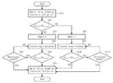
도 6은 본 발명의 실시 예에 따른 위상 자동 보정 동작의 알고리즘을 설명하기 위한 흐름도이다.6 is a flowchart illustrating an algorithm of an automatic phase correction operation according to an embodiment of the present invention.
도 1부터 도 6을 참조하여 위상 자동 보정 동작을 설명하면 다음과 같다.A phase automatic correction operation will be described with reference to FIGS. 1 to 6 as follows.
우선, 카운터(54)는 로우 레벨을 갖는 보정 제어 신호(Cal_end)를 발생한다. 도 1에는 보정 제어 신호(Cal_end)를 카운터(54)가 발생하는 것으로 도시되어 있으나 실시 예에 따라 컨트롤러(미 도시)가 보정 제어 신호(Cal_end)를 발생할 수 있다. 스위치(SW; 42), 각 위상 검출기(44-1과 44-5), 비교기(COMP; 48), 카운터(54), 및 클락 발생기(52)는 로우 레벨을 갖는 보정 제어 신호(Cal_end)에 응답하여 인에이블되고 제1믹서(70)와 제2믹서(72)는 디스에이블된다(S10).First, the
비교기(48)는 제1필터 신호(DCXOR)의 DC레벨과 제2필터 신호(DCXNOR)의 DC레벨을 서로 비교한다. 제1필터 신호(DCXOR)의 DC레벨이 제2필터 신호(DCXNOR)의 DC레벨보다 높은 경우(S20), 즉 출력 I신호(OUT_IP)의 위상과 출력 Q신호(OUT_QP)의 위상의 차이가 90도보다 큰 경우 카운터(54)의 MSB는 0이 된다(S30). 따라서 카운터(54)는 두 신호들(OUT_IP와 OUT_QP)의 위상 차이를 감소시키기 위하여 다운-카운트되는 디지털 코드(CODE)를 출력한다(S40).The
계속하여 비교기(48)는 제1필터 신호(DCXOR)의 DC 레벨과 제2필터 신호 (DCXNOR)의 DC 레벨을 비교한다(S50). 제1필터 신호(DCXOR)의 DC 레벨이 제2필터 신호 (DCXNOR)의 DC레벨보다 여전히 높은 경우, 카운터(54)는 현재의 디지털 코드(CODE)가 최대 값인지의 여부를 판단한다(S60).Next, the
현재의 디지털 코드(CODE)가 최대값이 될 때까지 카운터(54)는 S40과 S50을 반복적으로 수행한다. S40과 S50의 결과로서 현재의 디지털 코드(CODE)가 최대값인 경우 위상 자동 보정 동작은 종료된다. 또한, S40의 결과로서 두 신호들(OUT_IP와 OUT_QP)의 위상 차이가 90도로 감소하는 경우 위상 자동 보정 동작은 종료된다.The
따라서 카운터(54)는 하이 레벨을 갖는 위상 제어 신호(Cal_end)를 출력한다. 따라서, 스위치(42), 각 위상 검출기(44-1과 44-5), 및 비교기(COMP; 48)는 디스에이블되고 카운터(54)와 클릭 발생기(52)는 인에이블 상태를 유지한다(S70). 그러나, 클릭 발생기(52) 클락 신호(CLKcal)를 출력하기 않으므로 카운터(54)는 위상 제어 신호(Cal_end)가 하이 레벨로 천이하기 직전의 디지털 코드(CODE)를 유대로 유지한다.Accordingly, the
S20의 판단 결과로서 제1필터 신호(DCXOR)의 DC레벨이 제2필터 신호(DCXNOR)의 DC레벨보다 작은 경우, 즉, 출력 I신호(OUT_IP)의 위상과 출력 Q신호(OUT_QP)의 위상의 차이가 90도보다 작은 경우, 카운터(54)의 MSB는 1이 된다(S80). 따라서 카운터(54)는 두 신호들(OUT_IP와 OUT_QP)의 위상 차이를 증가시키기 위하여 업-카운트되는 디지털 코드(CODE)를 출력한다(S90).As a determination result of S20 of the first filter signal (DCXOR) when the DC level is smaller than the DC level of the second filter signal (DCXNOR), that is, the output I signal (OUT_IP) phase and the output Q signal (OUT_QP) of If the difference in phase is smaller than 90 degrees, the MSB of the
계속하여 비교기(48)는 제1필터 신호(DCXOR)의 DC 레벨과 제2필터 신호 (DCXNOR)의 DC 레벨을 비교한다(S100). 제1필터 신호(DCXOR)의 DC 레벨이 제2필터 신호(DCXNOR)의 DC레벨보다 여전히 늦은 경우, 카운터(54)는 현재의 디지털 코드(CODE)가 최소값인지 판단한다(S110).Next, the
현재의 디지털 코드(CODE)가 최소값이 될 때까지 카운터(54)는 S90과 S100을 반복적으로 수행한다. S90과 S100의 결과로서 현재의 디지털 코드(CODE)가 최소값인 경우 위상 자동 보정 동작은 종료된다. 또한, S100의 결과로서 두 신호들 (OUT_IP와 OUT_QP)의 위상 차이가 90도로 감소하는 경우 위상 자동 보정 동작은 종료된다.The
따라서 카운터(54)는 하이 레벨을 갖는 위상 제어 신호(Cal_end)를 출력한다. 따라서, 스위치(42), 각 위상 검출기(44-1과 44-5), 및 비교기(COMP; 48)는 디스에이블되고 카운터(54)와 클릭 발생기(52)는 인에이블 상태를 유지한다(S70). 그러나, 클릭 발생기(52) 클락 신호(CLKcal)를 출력하기 않으므로 카운터(54)는 위상 제어 신호(Cal_end)가 하이 레벨로 천이하기 직전의 디지털 코드(CODE)를 그대로 유지한다.Accordingly, the
상기 본 발명의 내용은 도면에 도시된 일실시 예를 참고로 설명되었으나 이는 예시적인 것에 불과하며, 본 기술 분야의 통상의 지식을 가진 자라면 이로부터 다양한 변형 및 균등한 타 실시 예가 가능하다는 점을 이해할 것이다. 따라서 본 발명의 전정한 기술적 보호 범위는 첨부된 특허청구범위의 기술적 사상에 의해 정해져야 할 것이다.Although the contents of the present invention have been described with reference to one embodiment shown in the drawings, this is merely exemplary, and various modifications and equivalent other embodiments may be made by those skilled in the art. I will understand. Therefore, the technical protection scope of the present invention should be defined by the technical spirit of the appended claims.
도 1은 본 발명의 일 실시 예에 따른 위상 자동 보정 회로를 포함하는 송신기를 나타내는 블록도이다.1 is a block diagram illustrating a transmitter including a phase automatic correction circuit according to an embodiment of the present invention.
도 2는 도 1에 도시된 제1버퍼, 제2버퍼, 및 위상 보정 회로를 좀 더 상세히 나타내는 도면이다.FIG. 2 is a diagram illustrating the first buffer, the second buffer, and the phase correction circuit shown in FIG. 1 in more detail.
도 3은 도 2에 도시된 각 전류 모드 로직의 동작을 설명하기 위한 도면이다.FIG. 3 is a diagram for describing an operation of each current mode logic illustrated in FIG. 2.
도 4는 도 2에 도시된 각 전류 모드 로직의 동작을 설명하기 위한 다른 도면이다.4 is another diagram for describing an operation of each current mode logic illustrated in FIG. 2.
도 5는 도 1에 도시된 카운터의 동작을 제어하는 제어신호들의 타이밍도이다.FIG. 5 is a timing diagram of control signals for controlling the operation of the counter shown in FIG. 1.
도 6은 본 발명의 실시 예에 따른 위상 자동 보정 동작의 알고리즘을 설명하기 위한 흐름도이다.6 is a flowchart illustrating an algorithm of an automatic phase correction operation according to an embodiment of the present invention.
Claims (10)
Translated fromKoreanPriority Applications (3)
| Application Number | Priority Date | Filing Date | Title |
|---|---|---|---|
| KR1020090082144AKR20110024236A (en) | 2009-09-01 | 2009-09-01 | Phase correction method, phase correction circuit, and signal processing apparatus comprising the same |
| US12/836,325US8344309B2 (en) | 2009-09-01 | 2010-07-14 | Method and circuit for calibrating phase, and signal processing apparatus having the same |
| JP2010195568AJP2011055498A (en) | 2009-09-01 | 2010-09-01 | Phase-correction method, phase-correction circuit, and signal processor containing the same |
Applications Claiming Priority (1)
| Application Number | Priority Date | Filing Date | Title |
|---|---|---|---|
| KR1020090082144AKR20110024236A (en) | 2009-09-01 | 2009-09-01 | Phase correction method, phase correction circuit, and signal processing apparatus comprising the same |
Publications (1)
| Publication Number | Publication Date |
|---|---|
| KR20110024236Atrue KR20110024236A (en) | 2011-03-09 |
Family
ID=43624044
Family Applications (1)
| Application Number | Title | Priority Date | Filing Date |
|---|---|---|---|
| KR1020090082144AWithdrawnKR20110024236A (en) | 2009-09-01 | 2009-09-01 | Phase correction method, phase correction circuit, and signal processing apparatus comprising the same |
Country Status (3)
| Country | Link |
|---|---|
| US (1) | US8344309B2 (en) |
| JP (1) | JP2011055498A (en) |
| KR (1) | KR20110024236A (en) |
Families Citing this family (6)
| Publication number | Priority date | Publication date | Assignee | Title |
|---|---|---|---|---|
| US20130261806A1 (en)* | 2012-03-27 | 2013-10-03 | Lennox Industries Inc. | Heating, ventilation and air conditioning system user interface having accurized temperature sensor configuration and method of operation thereof |
| US9160582B1 (en)* | 2014-03-31 | 2015-10-13 | Cadence Design Systems, Inc. | System and method for phase recovery with selective mitigation of timing corruption due to digital receiver equalization |
| KR20160149717A (en)* | 2015-06-19 | 2016-12-28 | 에스케이하이닉스 주식회사 | Semiconductor device and operating method thereof |
| US9768792B1 (en)* | 2016-12-30 | 2017-09-19 | Itron, Inc. | Asynchronous sigma-delta analog-to-digital converter |
| US10459856B2 (en) | 2016-12-30 | 2019-10-29 | Itron, Inc. | Variable acquisition buffer length |
| US10841072B2 (en)* | 2018-12-05 | 2020-11-17 | Samsung Electronics Co., Ltd. | System and method for providing fast-settling quadrature detection and correction |
Family Cites Families (13)
| Publication number | Priority date | Publication date | Assignee | Title |
|---|---|---|---|---|
| JPS6212215A (en)* | 1985-07-10 | 1987-01-21 | Hitachi Ltd | frequency converter |
| JPH02302130A (en)* | 1989-05-17 | 1990-12-14 | Hitachi Ltd | Frequency conversion circuit, phase correction device used therefor, variable phase shifter used for relevant phase correction device and television receiver using the same frequency conversion circuit |
| JPH07303028A (en)* | 1994-05-09 | 1995-11-14 | Hitachi Ltd | 90 degree phase shift circuit |
| GB2326037A (en) | 1997-06-06 | 1998-12-09 | Nokia Mobile Phones Ltd | Maintaining signals in phase quadrature |
| JP3098464B2 (en)* | 1997-06-26 | 2000-10-16 | 日本電気アイシーマイコンシステム株式会社 | 90 degree phase shift circuit |
| JP2001339294A (en)* | 2000-05-30 | 2001-12-07 | Mitsubishi Electric Corp | DLL circuit |
| US6891440B2 (en)* | 2000-10-02 | 2005-05-10 | A. Michael Straub | Quadrature oscillator with phase error correction |
| US6704551B2 (en)* | 2001-02-21 | 2004-03-09 | Koninklijke Philips Electronics N.V. | Calibration of in-phase and quadrature transmit branches of a transmitter |
| US7146146B2 (en) | 2003-01-31 | 2006-12-05 | Ditrans Ip, Inc. | Systems and methods for coherent adaptive calibration in a receiver |
| JP3926324B2 (en)* | 2003-12-19 | 2007-06-06 | 埼玉日本電気株式会社 | Digital modulation circuit |
| US7254379B2 (en)* | 2004-07-09 | 2007-08-07 | Silicon Storage Technology, Inc. | RF receiver mismatch calibration system and method |
| JP2008078995A (en)* | 2006-09-21 | 2008-04-03 | Nec Electronics Corp | Phase shifting circuit |
| KR101334923B1 (en) | 2007-03-09 | 2013-11-29 | 삼성전자주식회사 | Apparatus and method quadrature modulation in communication system |
- 2009
- 2009-09-01KRKR1020090082144Apatent/KR20110024236A/ennot_activeWithdrawn
- 2010
- 2010-07-14USUS12/836,325patent/US8344309B2/enactiveActive
- 2010-09-01JPJP2010195568Apatent/JP2011055498A/enactivePending
Also Published As
| Publication number | Publication date |
|---|---|
| US20110050474A1 (en) | 2011-03-03 |
| US8344309B2 (en) | 2013-01-01 |
| JP2011055498A (en) | 2011-03-17 |
Similar Documents
| Publication | Publication Date | Title |
|---|---|---|
| US8253454B2 (en) | Phase lock loop with phase interpolation by reference clock and method for the same | |
| KR20110024236A (en) | Phase correction method, phase correction circuit, and signal processing apparatus comprising the same | |
| US7336112B1 (en) | False lock protection in a delay-locked loop (DLL) | |
| US6133797A (en) | Self calibrating VCO correction circuit and method of operation | |
| US7869769B2 (en) | Method and apparatus for reconfigurable frequency generation | |
| TWI381646B (en) | Loop bandwidth control apparatus and method of phase locked loop | |
| US20150381344A1 (en) | Semiconductor device | |
| US7603096B2 (en) | Mixer with self-calibrating carrier leakage mechanism | |
| US20150222273A1 (en) | Apparatus and methods for phase-locked loops with soft transition from holdover to reacquiring phase lock | |
| WO2001065698A1 (en) | Dc offset correction adaptable to multiple requirements | |
| US8149033B2 (en) | Phase control device, phase-control printed board, and control method | |
| US8283984B2 (en) | Method and apparatus of phase locking for reducing clock jitter due to charge leakage | |
| KR20170083816A (en) | Digital phase locked loop and driving method thereof | |
| CN113676178A (en) | Phase-locked loop circuit and digital time converter error elimination method | |
| US20100134157A1 (en) | PLL circuit and method of cotrolling the same | |
| US7492297B2 (en) | Digital-to-analog converter and method thereof | |
| EP1241791B1 (en) | PLL frequency synthesizer | |
| CN112187229B (en) | High-precision pulse width modulation system and method | |
| US9853650B1 (en) | Method and apparatus of frequency synthesis | |
| US7576577B2 (en) | Device for static phase error compensation in a phase-lock loop system with a symmetrical structure | |
| JP2001285059A (en) | Self-correction circuit and method for correcting phase offset between ring oscillator output waveforms | |
| US7541879B2 (en) | System for compensation of VCO non-linearity | |
| KR100717134B1 (en) | Automatic frequency control loop circuit | |
| US20060170468A1 (en) | PLL circuit and program for same | |
| EP0690564A1 (en) | Method and apparatus for sensing common mode error |
Legal Events
| Date | Code | Title | Description |
|---|---|---|---|
| PA0109 | Patent application | Patent event code:PA01091R01D Comment text:Patent Application Patent event date:20090901 | |
| PG1501 | Laying open of application | ||
| PC1203 | Withdrawal of no request for examination | ||
| WITN | Application deemed withdrawn, e.g. because no request for examination was filed or no examination fee was paid |