KR20110001718A - Method for forming semiconductor device - Google Patents
Method for forming semiconductor deviceDownload PDFInfo
- Publication number
- KR20110001718A KR20110001718AKR1020090059379AKR20090059379AKR20110001718AKR 20110001718 AKR20110001718 AKR 20110001718AKR 1020090059379 AKR1020090059379 AKR 1020090059379AKR 20090059379 AKR20090059379 AKR 20090059379AKR 20110001718 AKR20110001718 AKR 20110001718A
- Authority
- KR
- South Korea
- Prior art keywords
- pattern
- layer
- forming
- poly
- photoresist pattern
- Prior art date
- Legal status (The legal status is an assumption and is not a legal conclusion. Google has not performed a legal analysis and makes no representation as to the accuracy of the status listed.)
- Withdrawn
Links
- 238000000034methodMethods0.000titleclaimsabstractdescription102
- 239000004065semiconductorSubstances0.000titleclaimsabstractdescription20
- 125000006850spacer groupChemical group0.000claimsabstractdescription57
- 229920002120photoresistant polymerPolymers0.000claimsabstractdescription50
- 238000005530etchingMethods0.000claimsabstractdescription41
- 230000008569processEffects0.000claimsdescription55
- BOTDANWDWHJENH-UHFFFAOYSA-NTetraethyl orthosilicateChemical compoundCCO[Si](OCC)(OCC)OCCBOTDANWDWHJENH-UHFFFAOYSA-N0.000claimsdescription23
- 238000000151depositionMethods0.000claimsdescription9
- 238000007654immersionMethods0.000claimsdescription3
- 238000007517polishing processMethods0.000claimsdescription3
- 239000000126substanceSubstances0.000claimsdescription3
- 238000001039wet etchingMethods0.000claimsdescription3
- 239000007788liquidSubstances0.000claims1
- 238000004519manufacturing processMethods0.000description13
- 239000000463materialSubstances0.000description11
- 229910052581Si3N4Inorganic materials0.000description5
- 238000000059patterningMethods0.000description5
- HQVNEWCFYHHQES-UHFFFAOYSA-Nsilicon nitrideChemical compoundN12[Si]34N5[Si]62N3[Si]51N64HQVNEWCFYHHQES-UHFFFAOYSA-N0.000description5
- 229910003481amorphous carbonInorganic materials0.000description4
- 230000015572biosynthetic processEffects0.000description4
- 238000005516engineering processMethods0.000description4
- 230000008021depositionEffects0.000description3
- XUIMIQQOPSSXEZ-UHFFFAOYSA-NSiliconChemical compound[Si]XUIMIQQOPSSXEZ-UHFFFAOYSA-N0.000description2
- 238000007792additionMethods0.000description2
- 238000000231atomic layer depositionMethods0.000description2
- 230000008901benefitEffects0.000description2
- 238000012986modificationMethods0.000description2
- 230000004048modificationEffects0.000description2
- 229910052710siliconInorganic materials0.000description2
- 239000010703siliconSubstances0.000description2
- 238000006467substitution reactionMethods0.000description2
- 239000006117anti-reflective coatingSubstances0.000description1
- 230000004888barrier functionEffects0.000description1
- 239000011248coating agentSubstances0.000description1
- 238000000576coating methodMethods0.000description1
- 238000007796conventional methodMethods0.000description1
- 230000003247decreasing effectEffects0.000description1
- 238000013461designMethods0.000description1
- 238000011161developmentMethods0.000description1
- 238000007687exposure techniqueMethods0.000description1
- 230000006872improvementEffects0.000description1
- 238000002955isolationMethods0.000description1
- 238000005192partitionMethods0.000description1
- 230000002093peripheral effectEffects0.000description1
- 239000003504photosensitizing agentSubstances0.000description1
- 238000012545processingMethods0.000description1
- 229910052814silicon oxideInorganic materials0.000description1
- WNUPENMBHHEARK-UHFFFAOYSA-Nsilicon tungstenChemical compound[Si].[W]WNUPENMBHHEARK-UHFFFAOYSA-N0.000description1
- 239000002210silicon-based materialSubstances0.000description1
- 239000000758substrateSubstances0.000description1
- 230000008646thermal stressEffects0.000description1
- 239000011800void materialSubstances0.000description1
Images


Classifications
- G—PHYSICS
- G03—PHOTOGRAPHY; CINEMATOGRAPHY; ANALOGOUS TECHNIQUES USING WAVES OTHER THAN OPTICAL WAVES; ELECTROGRAPHY; HOLOGRAPHY
- G03F—PHOTOMECHANICAL PRODUCTION OF TEXTURED OR PATTERNED SURFACES, e.g. FOR PRINTING, FOR PROCESSING OF SEMICONDUCTOR DEVICES; MATERIALS THEREFOR; ORIGINALS THEREFOR; APPARATUS SPECIALLY ADAPTED THEREFOR
- G03F7/00—Photomechanical, e.g. photolithographic, production of textured or patterned surfaces, e.g. printing surfaces; Materials therefor, e.g. comprising photoresists; Apparatus specially adapted therefor
- G03F7/70—Microphotolithographic exposure; Apparatus therefor
- G03F7/70216—Mask projection systems
- G03F7/70341—Details of immersion lithography aspects, e.g. exposure media or control of immersion liquid supply
- H—ELECTRICITY
- H01—ELECTRIC ELEMENTS
- H01L—SEMICONDUCTOR DEVICES NOT COVERED BY CLASS H10
- H01L21/00—Processes or apparatus adapted for the manufacture or treatment of semiconductor or solid state devices or of parts thereof
- H01L21/02—Manufacture or treatment of semiconductor devices or of parts thereof
- H01L21/027—Making masks on semiconductor bodies for further photolithographic processing not provided for in group H01L21/18 or H01L21/34
- H01L21/033—Making masks on semiconductor bodies for further photolithographic processing not provided for in group H01L21/18 or H01L21/34 comprising inorganic layers
- H01L21/0334—Making masks on semiconductor bodies for further photolithographic processing not provided for in group H01L21/18 or H01L21/34 comprising inorganic layers characterised by their size, orientation, disposition, behaviour, shape, in horizontal or vertical plane
- H01L21/0337—Making masks on semiconductor bodies for further photolithographic processing not provided for in group H01L21/18 or H01L21/34 comprising inorganic layers characterised by their size, orientation, disposition, behaviour, shape, in horizontal or vertical plane characterised by the process involved to create the mask, e.g. lift-off masks, sidewalls, or to modify the mask, e.g. pre-treatment, post-treatment
- H—ELECTRICITY
- H01—ELECTRIC ELEMENTS
- H01L—SEMICONDUCTOR DEVICES NOT COVERED BY CLASS H10
- H01L21/00—Processes or apparatus adapted for the manufacture or treatment of semiconductor or solid state devices or of parts thereof
- H01L21/02—Manufacture or treatment of semiconductor devices or of parts thereof
- H01L21/027—Making masks on semiconductor bodies for further photolithographic processing not provided for in group H01L21/18 or H01L21/34
- H01L21/033—Making masks on semiconductor bodies for further photolithographic processing not provided for in group H01L21/18 or H01L21/34 comprising inorganic layers
- H01L21/0334—Making masks on semiconductor bodies for further photolithographic processing not provided for in group H01L21/18 or H01L21/34 comprising inorganic layers characterised by their size, orientation, disposition, behaviour, shape, in horizontal or vertical plane
- H01L21/0338—Process specially adapted to improve the resolution of the mask
- H—ELECTRICITY
- H01—ELECTRIC ELEMENTS
- H01L—SEMICONDUCTOR DEVICES NOT COVERED BY CLASS H10
- H01L21/00—Processes or apparatus adapted for the manufacture or treatment of semiconductor or solid state devices or of parts thereof
- H01L21/02—Manufacture or treatment of semiconductor devices or of parts thereof
- H01L21/04—Manufacture or treatment of semiconductor devices or of parts thereof the devices having potential barriers, e.g. a PN junction, depletion layer or carrier concentration layer
- H01L21/18—Manufacture or treatment of semiconductor devices or of parts thereof the devices having potential barriers, e.g. a PN junction, depletion layer or carrier concentration layer the devices having semiconductor bodies comprising elements of Group IV of the Periodic Table or AIIIBV compounds with or without impurities, e.g. doping materials
- H01L21/30—Treatment of semiconductor bodies using processes or apparatus not provided for in groups H01L21/20 - H01L21/26
- H01L21/31—Treatment of semiconductor bodies using processes or apparatus not provided for in groups H01L21/20 - H01L21/26 to form insulating layers thereon, e.g. for masking or by using photolithographic techniques; After treatment of these layers; Selection of materials for these layers
- H01L21/3105—After-treatment
- H01L21/311—Etching the insulating layers by chemical or physical means
- H01L21/31144—Etching the insulating layers by chemical or physical means using masks
- H—ELECTRICITY
- H01—ELECTRIC ELEMENTS
- H01L—SEMICONDUCTOR DEVICES NOT COVERED BY CLASS H10
- H01L21/00—Processes or apparatus adapted for the manufacture or treatment of semiconductor or solid state devices or of parts thereof
- H01L21/02—Manufacture or treatment of semiconductor devices or of parts thereof
- H01L21/04—Manufacture or treatment of semiconductor devices or of parts thereof the devices having potential barriers, e.g. a PN junction, depletion layer or carrier concentration layer
- H01L21/18—Manufacture or treatment of semiconductor devices or of parts thereof the devices having potential barriers, e.g. a PN junction, depletion layer or carrier concentration layer the devices having semiconductor bodies comprising elements of Group IV of the Periodic Table or AIIIBV compounds with or without impurities, e.g. doping materials
- H01L21/30—Treatment of semiconductor bodies using processes or apparatus not provided for in groups H01L21/20 - H01L21/26
- H01L21/31—Treatment of semiconductor bodies using processes or apparatus not provided for in groups H01L21/20 - H01L21/26 to form insulating layers thereon, e.g. for masking or by using photolithographic techniques; After treatment of these layers; Selection of materials for these layers
- H01L21/3205—Deposition of non-insulating-, e.g. conductive- or resistive-, layers on insulating layers; After-treatment of these layers
- H01L21/321—After treatment
- H01L21/3213—Physical or chemical etching of the layers, e.g. to produce a patterned layer from a pre-deposited extensive layer
- H01L21/32139—Physical or chemical etching of the layers, e.g. to produce a patterned layer from a pre-deposited extensive layer using masks
Landscapes
- Engineering & Computer Science (AREA)
- Physics & Mathematics (AREA)
- General Physics & Mathematics (AREA)
- Condensed Matter Physics & Semiconductors (AREA)
- Manufacturing & Machinery (AREA)
- Computer Hardware Design (AREA)
- Microelectronics & Electronic Packaging (AREA)
- Power Engineering (AREA)
- Chemical & Material Sciences (AREA)
- Inorganic Chemistry (AREA)
- Internal Circuitry In Semiconductor Integrated Circuit Devices (AREA)
Abstract
Translated fromKoreanDescription
Translated fromKorean본 발명은 반도체 소자 형성 방법에 관한 것으로, 더욱 상세하게는 네거티브 톤 SPT 방법을 적용할 때 상호 접속(interconnection) 영역의 구현이 힘든 패드 레이아웃을 구현하는 데 있어 제조 공정 시 오버레이 마진을 증대시킬 수 있는 반도체 소자 형성 방법에 관한 것이다.The present invention relates to a method of forming a semiconductor device, and more particularly, in the implementation of a pad layout in which interconnect areas are difficult to implement when applying a negative tone SPT method, an overlay margin can be increased during a manufacturing process. A method for forming a semiconductor device.
반도체 소자가 고집적화됨에 따라 반도체 소자를 구성하는 회로를 구현하는 패턴의 크기 및 간격(pitch)이 점점 감소하고 있다. 레일레이(Rayleigh) 방정식을 살펴보면, 반도체 소자 내 미세 패턴의 크기는 노광 공정에 사용되는 빛의 파장에 비례하고 렌즈의 크기에 반비례한다. 따라서, 미세 패턴 형성을 위해, 지금까지 노광 공정에 사용되는 빛의 파장을 줄이거나 렌즈의 크기를 크게 하는 방법을 주로 사용되어 왔다.As semiconductor devices are highly integrated, the size and pitch of patterns for implementing circuits constituting semiconductor devices are gradually decreasing. Looking at the Rayleigh equation, the size of the fine pattern in the semiconductor device is proportional to the wavelength of light used in the exposure process and inversely proportional to the size of the lens. Therefore, a method of reducing the wavelength of light or increasing the size of the lens used in the exposure process has been mainly used for forming a fine pattern.
또한, 가공 공정 중 사진 공정 기술은 마스크 설계를 정교하게 해줌으로써 마스크를 통해 나오는 빛의 양을 적절히 조절하고, 새로운 감광제의 개발, 고구경(high numerical aperture) 렌즈를 사용하는 스캐너(scanner)의 개발, 변형된 마스크를 개발하는 등의 노력에 의해 반도체 소자 제조 장치가 갖고 있는 기술적인 한계를 극복하고 있다. 하지만, 현재 사용되는 광원(예를 들면, KrF, ArF 등)을 사용하여 진행하는 노광 및 해상 능력의 한계로 인하여 원하는 패턴의 폭 및 간격을 형성하기 어려운 실정이다. 일례로, 현재까지는 60nm 정도의 패턴 크기를 제조할 수 있는 노광 기술이 개발되어 있으나 그 이하의 패턴 크기를 제조하는 데에는 어려움이 많다.In addition, in-process photo processing technology refines the mask design to properly control the amount of light that passes through the mask, develop new photosensitizers, and develop scanners using high numerical aperture lenses. By overcoming efforts to develop modified masks, the technical limitations of semiconductor device manufacturing apparatuses have been overcome. However, due to limitations in exposure and resolution ability that proceed using current light sources (for example, KrF, ArF, etc.), it is difficult to form a width and an interval of a desired pattern. For example, until now, exposure techniques for manufacturing a pattern size of about 60 nm have been developed, but there are many difficulties in manufacturing a pattern size smaller than that.
광원의 한계를 극복하기 위한 미세 패턴의 크기 및 간격을 갖는 감광막 패턴을 형성하기 위한 여러 가지 연구가 계속되고 있다. 그 중의 한 가지 방법은 두 번의 사진 공정을 수행하여 패턴을 형성하는 DPT(Double Patterning Technology) 방법이 있다. DPT 방법에는 패턴 주기의 두 배의 주기를 가지는 패턴을 노광하고 식각한 후 그 사이 사이에 똑같은 두 배 주기를 갖는 두 번째 패턴을 노광하고 식각하는 DE2T(Double Expose Etch Technology) 방법과, 스페이서를 이용하여 패턴을 형성하는 SPT(Spacer Patterning Technology) 방법이 있다. DE2T 방법 및 SPT 방법은 각각 네거티브 톤(Negative Tone)과 포지티브 톤(Positive Tone)의 공정으로 각각 형성할 수 있다.Various studies have been conducted to form a photosensitive film pattern having a size and a gap of a fine pattern to overcome the limitation of the light source. One method is a double patterning technology (DPT) method in which a pattern is formed by performing two photographic processes. The DPT method uses a DE2T (Double Expose Etch Technology) method that exposes and etches a pattern having twice the period of the pattern period, and then exposes and etches a second pattern having the same double period between them, and a spacer. There is a SPT (Spacer Patterning Technology) method of forming a pattern. The DE2T method and the SPT method may be respectively formed by a process of negative tones and positive tones, respectively.
네거티브 톤 DE2T 방법은 첫 번째 마스크 공정에서 형성된 패턴을 두 번째 마스크 공정에서 제거하고 원하는 패턴을 형성하는 방법이고, 포지티브 톤 DE2T 방법은 첫 번째 마스크 공정과 두 번째 마스크 공정에서 형성한 패턴을 합쳐서 원하는 패턴을 형성하는 방법이다. 그러나, 첫 번째 마스크 공정과 식각 공정 후에 두 번째 마스크 공정과 식각 공정을 함으로서 원하는 패턴의 집적도를 얻을 수 있는 DE2T 방법은 두 번의 마스크 공정과 식각 공정을 수행하기 위해 필요한 추가 공정 의 수가 늘어나 공정의 복잡도가 증가시키는 단점이 있다. 또한, 통상적으로 오버레이(overlay)라고 불리는 서로 독립적인 첫 번째 마스크 공정과 두 번째 마스크 공정을 통해 얻은 패턴에 정렬 오차가 발생할 가능성이 있다.The negative tone DE2T method removes the pattern formed in the first mask process from the second mask process and forms a desired pattern. The positive tone DE2T method combines the pattern formed in the first mask process and the second mask process to form a desired pattern. How to form. However, the DE2T method, which achieves the desired pattern density by performing the second mask process and etching process after the first mask process and etching process, increases the complexity of the process by increasing the number of additional processes required to perform the second mask process and etching process. There is a disadvantage to increase. In addition, there is a possibility that alignment errors occur in the patterns obtained through the first mask process and the second mask process that are independent of each other, commonly referred to as overlay.
반면, SPT 방법은 셀 영역의 패터닝을 위해 마스크 공정이 한 번만 진행되므로 오 정렬(misalign)의 단점을 방지할 수 있는 자기 정렬(self align) 방법이다. 그러나, 코어 및 주변회로 영역에 있는 패드 패턴을 형성하기 위해 매트 에지(mat edge) 영역의 패턴 부분을 분리하기 위해 추가적인 마스크 공정이 필요하며, 스페이서 형성 지역의 증착 균일성(deposition uniformity)과 스페이서 형성 식각 공정에서 비롯된 CD 제어가 용이하지 않아 CD 균일성(uniformity)이 문제가 된다.On the other hand, the SPT method is a self align method that can prevent the disadvantage of misalign because the mask process is performed only once for patterning the cell region. However, an additional mask process is required to separate the pattern portion of the mat edge region to form the pad pattern in the core and peripheral circuit regions, and the deposition uniformity of the spacer formation region and the spacer formation. CD uniformity due to the etching process is not easy, so CD uniformity is a problem.
도 1a 내지 도 1g는 네거티브 톤 SPT(negative tone Spacer Patterning Technology) 방법을 나타낸 단면도이다. 여기서는 플래시 메모리(flash memory)의 제어 게이트(control gate)를 형성하는 경우를 예를 들어 설명한다.1A to 1G are cross-sectional views illustrating a negative tone SPT method. Here, an example of forming a control gate of a flash memory will be described.
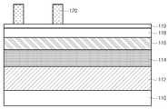
도 1a를 참조하면, 반도체 기판에 활성영역을 정의하는 소자 분리막을 형성한 후 ONO 유전막/게이트 폴리/텅스텐 실리사이드(WSi) 등이 증착되어 구현된 하부 구조 상부에 캡핑(capping) 제 1 실리콘 질산화막(SiON)(110)을 형성한다. 제 1 실리콘 질산화막(110) 상부에 하드 마스크로서 제 1 TEOS(112) 및 제 1 폴리(114)를 증착한다. 여기서, 제 1 폴리(114)로 형성하는 하드 마스크의 높이는 분할 패턴(partition)으로서 SPT 공정의 핵심이 되는 스페이서의 높이를 결정한다.Referring to FIG. 1A, after forming an isolation layer defining an active region on a semiconductor substrate, a capping first silicon oxynitride layer is formed on an upper structure formed by depositing an ONO dielectric film / gate poly / tungsten silicide (WSi) or the like. (SiON) 110 is formed. The
그러나, 감광막 패턴으로는 제 1 폴리(114)를 식각할 수 없기 때문에 제 1 폴리(114)를 식각하기 위한 하드 마스크로서 제 1 비정질 탄소(116) 및 제 2 실리콘 질산화막(118)을 제 1 폴리(114) 상부에 형성한다. 이어서, 제 2 실리콘 질산화막(118) 상부에 하부 반사 방지막(Bottom Anti-Reflected Coating(BARC) layer, 119)를 형성한다.However, since the
BARC(119) 상부에 감광막을 도포하고, 원하는 피치의 2배 피치를 갖는 패턴이 정의된 마스크를 이용하여 감광막에 대해 노광 및 현상 공정을 통해 감광막 패턴(120)을 형성한다. 예를 들어 식각 바이어스(etch bias)를 고려하지 않는 경우, 라인이 40nm CD(Critical Dimension)로 형성되면 스페이스는 120nm의 CD로 형성한다. 즉, 라인/스페이스 비율이 1:3이 되도록 한다.The photoresist film is coated on the
도 1b를 참조하면, 감광막 패턴(120)을 식각 마스크로 이용하여 BARC(119), 제 2 실리콘 질산화막(118), 비정질 탄소(116) 및 제 1 폴리(114)를 순차적으로 식각하여 제 1 폴리 패턴(114a)을 형성하고, 감광막 패턴(120), BARC(119), 제 2 실리콘 질화막(118) 및 비정질 탄소(116)는 제거한다. 이때, 하드 마스크인 제 1 TEOS(112)의 상부를 추후 형성되는 스페이서의 두께만큼 부분 식각한다. 이렇게 식각하는 이유는 제 1 폴리 패턴(114a)의 높이와 TEOS(Tetraethyl Orthosilicate)로 형성될 스페이서의 두께를 동일하게 맞춰주기 위한 것이다. 제 1 폴리 패턴(114a)의 높이와 스페이서의 두께를 동일하게 하지 않을 경우, 스페이서를 식각하는 과정에서 식각 마스크(barrier)를 구성하는 물질의 차이로 인해 식각 선택비가 달라져 식각 프로파일(profile)이 달라질 수 있다. 이를 방지하기 위해, 하드 마스크인 제 1 TEOS(112)의 상부를 식각한다. 또한, 스페이서(122)의 형성 시, 제 1 폴리 패 턴(114a)과 하부 하드 마스크 제 1 TEOS(112)의 증착 온도보다 낮은 온도로 스페이서 물질로 증착해야 온도 영향(thermal stress)으로 인한 필름 리프팅(film lifting) 등을 방지할 수 있다.Referring to FIG. 1B, the
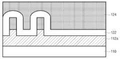
도 1c를 참조하면, 제 1 폴리 패턴(114a)을 포함하는 하드 마스크 제 1 TEOS(112) 상부에 스페이서 물질로 사용하는 제 2 TEOS(122)를 증착한다. 여기서는, 스페이서로서 사용되는 증착 물질이 선폭에 큰 영향을 미치기 때문에 스탭 커버리지(step coverage)가 우수한 제 2 TEOS(122)를 사용하는데, ALD(Atomic Layer Deposition)로 형성 가능한 물질을 사용할 수도 있다.Referring to FIG. 1C, a
도 1d 및 도 1e를 참조하면, 제 2 TEOS(122) 상부에 갭 필(gap fill) 하드 마스크 제 2 폴리(124)를 형성하고, 제 2 폴리(124)에 대해 에치백(etch back) 공정을 수행한다. 이때, 제 2 폴리(124)는 미세한 제 1 폴리 패턴(114a)이 형성된 영역에 상관없이 균일한 평탄면을 가질 수 있도록 충분히 증착되어야만 스페이서 물질인 제 2 TEOS(122)가 노출되도록 일정한 깊이를 식각할 때 도 1e에 도시된 바와 같은 제 2 폴리 패턴(124a)을 형성할 수 있다.1D and 1E, a gap fill hard mask
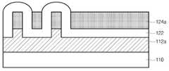
도 1f를 참조하면, 제 2 TEOS(122)를 부분 식각하여 제 1 폴리 패턴(114a)을 노출시켜, 스페이서 물질인 제 2 TEOS(122) 사이에 형성된 갭 필 하드 마스크 제 2 폴리 패턴(124a)이 제 1 폴리 패턴(114a)과 함께 라인 패턴을 형성하도록 한다. 여기서, 제 2 TEOS(122)를 식각하는 방법으로 건식 에치백(dry etch back) 및 습식 제거(wet strip) 방법을 적용한다.Referring to FIG. 1F, the
도 1g를 참조하면, 제 1 폴리 패턴(114a) 및 제 2 폴리 패턴(124a)을 식각 마스크로 이용하여 제 1 TEOS(112) 및 스페이서인 제 2 TEOS(122)를 식각하여 각각 제 1 TEOS 패턴(112a) 및 제 2 TEOS 패턴(122a)을 형성한다. 이 후 제 1 TEOS 패턴(112a) 및 제 2 TEOS 패턴(122a)을 식각 마스크로 이용하여 제 1 실리콘 질산화막(110)을 식각하여 기존의 노광 장비로는 형성할 수 없는 작은 피치를 갖는 미세 패턴을 형성한다.Referring to FIG. 1G, by using the
전술한 바와 같이, 도 1a 내지 도 1g에서 설명한 갭필 특성이 좋은 물질을 사용한 SPT공정은 하드마스크층을 증착하고 식각하는 공정을 여러번 반복하고 그때마다 형성되는 하드마스크 패턴에 따라 하부 절연층을 식각하는 공정을 수행하기 때문에, TAT (turn-around-time)가 증가하여 제조 원가가 높아지는 단점이 있다. 즉, 미세 패턴을 포함하는 반도체 장치의 제조 과정이 길어짐에 따라, 전술한 SPT 공정을 반도체 장치의 양산을 위해 적용하기 어렵다.As described above, the SPT process using the material having the good gap fill characteristics described with reference to FIGS. 1A to 1G repeats the process of depositing and etching the hard mask layer several times and etching the lower insulating layer according to the hard mask pattern formed at that time. Since the process is performed, there is a disadvantage that the turn-around-time (TAT) is increased to increase the manufacturing cost. That is, as the manufacturing process of the semiconductor device including the fine pattern becomes longer, it is difficult to apply the above-described SPT process for mass production of the semiconductor device.
전술한 문제를 극복하기 위해, 본 발명은 네거티브 SPT 방법을 적용하여 미세 패턴을 형성하는 과정에서 공정 수를 줄여 반도체 장치의 제조 원가를 낮출 수 있는 반도체 장치의 제조 방법을 제공한다.In order to overcome the above-described problem, the present invention provides a method of manufacturing a semiconductor device that can reduce the manufacturing cost of the semiconductor device by reducing the number of processes in the process of forming a fine pattern by applying the negative SPT method.
본 발명은 피식각층 상에 감광막 패턴을 형성하는 단계, 상기 감광막 패턴의 측벽에 스페이서를 형성하는 단계, 상기 감광막 패턴을 제거하는 단계, 상기 피식각층 및 상기 스페이서 상에 갭필 폴리층을 형성하는 단계, 상기 스페이서의 상부가 노출되도록 상기 갭필 폴리층을 평탄화하여 폴리 패턴을 형성하는 단계, 노출된 상기 스페이서막을 제거하는 단계, 및 상기 폴리 패턴을 식각마스크로 하여 상기 피식각층을 식각하는 단계를 포함하는 반도체 소자의 형성 방법을 제공한다.The present invention provides a method of forming a photoresist pattern on an etched layer, forming a spacer on sidewalls of the photoresist pattern, removing the photoresist pattern, forming a gapfill poly layer on the etched layer and the spacer, Forming a poly pattern by planarizing the gapfill poly layer to expose an upper portion of the spacer, removing the exposed spacer layer, and etching the etched layer using the poly pattern as an etch mask. Provided are a method of forming an element.
바람직하게는, 상기 감광막 패턴의 측벽에 스페이서를 형성하는 단계는 상기 피식각층 및 상기 감광막 패턴의 상부에 균일한 두께의 스페이서막을 형성하는 단계 및 상기 감광막 패턴이 노출되도록 상기 스페이서막을 식각하는 단계를 포함한다.Preferably, forming a spacer on a sidewall of the photoresist pattern includes forming a spacer layer having a uniform thickness on the etched layer and the photoresist pattern, and etching the spacer layer to expose the photoresist pattern. do.
바람직하게는, 상기 스페이서막을 식각하는 단계는 에치백 공정으로 수행되는 것을 특징으로 한다.Preferably, the etching of the spacer layer may be performed by an etch back process.
바람직하게는, 상기 폴리 패턴을 형성하는 단계는 에치백 공정, 화학적 기계적 연마공정 및 습식식각공정 중 하나의 방법을 사용하는 것을 특징으로 한다.Preferably, the forming of the poly pattern may be performed using one of an etch back process, a chemical mechanical polishing process, and a wet etching process.
바람직하게는, 상기 반도체 소자의 형성 방법은 상기 피식각층 및 상기 감광막 패턴 사이에 반사방지막을 증착하는 단계를 더 포함한다.Preferably, the method of forming the semiconductor device further comprises depositing an antireflection film between the etched layer and the photoresist pattern.
바람직하게는, 상기 반도체 소자의 형성 방법은 상기 감광막 패턴의 형성 후, 상기 감광막 패턴을 식각마스크로 사용하여 노출된 상기 반사방지막을 식각하는 단계를 더 포함한다.Preferably, the method of forming the semiconductor device further includes etching the exposed anti-reflection film using the photoresist pattern as an etching mask after the formation of the photoresist pattern.
바람직하게는, 상기 감광막 패턴의 하부에 남아있는 상기 반사방지막은 상기 감광막 패턴을 제거하는 공정시 함께 제거되는 것을 특징으로 한다.Preferably, the anti-reflection film remaining under the photoresist pattern is removed together during the process of removing the photoresist pattern.
바람직하게는, 상기 피식각층은 TEOS막을 포함하는 것을 특징으로 한다.Preferably, the etched layer is characterized in that it comprises a TEOS film.
바람직하게는, 상기 스페이서막은 산화막을 포함하는 것을 특징으로 한다.Preferably, the spacer film is characterized in that it comprises an oxide film.
바람직하게는, 상기 감광막 패턴의 형성시 ArF를 이용한 액침노광공정 및 ArF 또는 KrF를 이용한 노광공정 중 하나의 방법을 이용하는 것을 특징으로 한다.Preferably, the method of forming the photosensitive film pattern is one of an immersion exposure process using ArF and an exposure process using ArF or KrF.
본 발명은 네거티브 톤 SPT 방법을 적용할 때 절연막 등으로 이루어진 하드마스크 패턴 대신에 감광막 패턴의 측벽에 스페이서를 형성함으로써, 종래의 하드마스크층을 증착하고 하드마스크층을 노광공정을 통해 패터닝하는 과정을 크게 단순화 할 수 있어 TAT (turn-around-time)를 줄일 수 있는 장점이 있다.In the present invention, when the negative tone SPT method is applied, spacers are formed on sidewalls of the photoresist pattern instead of a hard mask pattern made of an insulating film, thereby depositing a conventional hard mask layer and patterning the hard mask layer through an exposure process. This can be greatly simplified, which reduces the turn-around-time (TAT).
또한, 본 발명은 동일한 공정을 통해 증착된 폴리층을 식각마스크로 사용할 수 있어, 종래에 서로 다른 공정을 통해 증착된 두 개의 폴리층으로 구성된 식각마스크를 이용하는 경우에 비해 하드마스크층이나 피식각층의 식각 시 균일도가 증가하는 장점이 있다.In addition, the present invention can use a poly layer deposited through the same process as an etching mask, compared to the case of using an etching mask consisting of two poly layers deposited through different processes in the prior art of the hard mask layer or the etching layer There is an advantage of increasing the uniformity during etching.
본 발명에서는 반도체 장치에 포함되는 미세 패턴을 형성하기 위한 방법 중 네거티브 SPT 공정을 단순화한다. 이하에서는 첨부한 도면을 참조하여 본 발명을 상세히 설명하기로 한다.In the present invention, a negative SPT process is simplified among the methods for forming a fine pattern included in a semiconductor device. Hereinafter, with reference to the accompanying drawings will be described in detail the present invention.
도 2a 내지 도 2i는 본 발명에 따른 SPT 방법을 통해 미세한 회로 패턴을 형성하는 제조 방법을 나타낸 단면도이다.2A to 2I are cross-sectional views illustrating a manufacturing method of forming a fine circuit pattern through the SPT method according to the present invention.
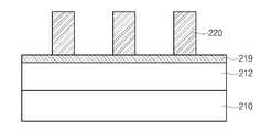
도 2a를 참조하면, 미세 패턴이 형성될 피식각층(210) 상에 감광막 패턴(220)을 형성한다. 피식각층(210) 상에는 하드마스크층(212)이 증착되어 있고, 하드마스크층(212) 상에는 반사방지막(219)이 증착된다. 여기서, 하드마스크층(212)은 TEOS막을 포함한다. 또한, 반사방지막(219) 상에는 감광막을 도포한 후 ArF를 이용한 액침노광공정 및 ArF 또는 KrF를 이용한 노광공정 중 하나의 방법을 이용하여 패터닝함으로써 감광막 패턴(220)을 형성할 수 있다. 감광막 패턴(220)의 선폭은 추후 형성되는 미세 패턴의 선폭과 동일하며, 감광막 패턴(220) 사이의 간격은 감광막 패턴(220)의 선폭의 두 배 이상이 되도록 한다.Referring to FIG. 2A, a
도 1a에 도시된 바와 같이 종래의 네거티브 SPT 공정을 수행할 때에는 제 1 TEOS(112)과 하부 반사 방지막(119) 사이에 제 1 폴리(114), 제 1 비정질 탄소(116) 및 제 2 실리콘 질산화막(118) 등의 복수의 절연층 또는 하드마스크층이 증착되었으나, 본 발명에서는 하드마스크층(212) 상에 직접 반사방지막(219)을 증착한 것에 큰 차이가 있다.As shown in FIG. 1A, when performing the conventional negative SPT process, the
도 2b를 참조하면, 감광막 패턴(220) 사이에 노출된 반사방지막(219)을 제 거하여 하드마스크층(212)을 노출시킨다.Referring to FIG. 2B, the
도 2c를 참조하면, 하드마스크층(212) 및 감광막 패턴(220) 상에 일정한 두께의 스페이서막(222)을 증착한다. 이때, 스페이서막(222)의 두께는 최종적으로 형성되는 미세 패턴 사이 간격이 되며, 스페이서막(222)은 산화막을 포함하는 것이 특징이다.Referring to FIG. 2C, a
도 2d를 참조하면, 감광막 패턴(220)과 하드마스크층(212)의 상부가 노출되도록 스페이서막(222)을 식각하여 스페이서(222)가 감광막 패턴(220)의 측벽에만 형성되도록 한다.Referring to FIG. 2D, the
도 2e를 참조하면, 노출된 감광막 패턴(220)을 제거하여 스페이서(222)만 하드마스크층(212)의 상부에 남도록 한다. 또한, 감광막 패턴(220)의 하부에 남아있던 반사방지막(219)도 제거한다. 즉, 감광막 패턴(220)이 제거될 때 감광막 패턴(220)의 측벽에 형성되어 있던 스페이서(222)는 제거되지 않고 일정한 간격만큼 이격된 패턴의 형상을 가지게 되며, 스페이서(222) 사이에는 하드마스크층(212)이 노출된다.Referring to FIG. 2E, the exposed
도 2f를 참조하면, 스페이서(222) 상에 폴리층(224)을 증착한다. 이때, 폴리층(224)은 갭필 특성이 우수한 물질을 사용하여 스페이서(222) 사이 공간에 빈공간없이 증착되도록 한다.Referring to FIG. 2F, a
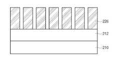
도 2g를 참조하면, 폴리층(224)을 스페이서(222)이 노출될 때까지 평탄화하여 폴리 패턴(226)을 형성한다. 이때, 폴리 패턴(226)을 형성하기 위해서, 에치백 공정, 화학적 기계적 연마공정 및 습식식각공정 중 하나의 방법을 사용하여 폴리 층(224)을 식각할 수 있다.Referring to FIG. 2G, the
도 2h를 참조하면, 폴리 패턴(226) 사이에 노출된 스페이서(222)을 제거하여 하드마스크층(212)의 일부를 노출시킨다.Referring to FIG. 2H, a portion of the
종래의 경우 폴리 패턴은 두 개의 서로 다른 공정을 통해 증착되기 때문에 동일한 물질을 사용하더라도 패턴의 균일도가 떨어지는 반면에, 본 발명의 일 실시예에 따른 제조 방법에 따라 형성된 폴리 패턴(226)은 종래와 달리 동일한 공정을 통해 증착된 물질로 구성되어 있어 종래보다 균일도가 향상된다. 폴리 패턴(226)의 균일도 향상은 피식각층(210) 내 형성되는 미세 패턴의 균일도를 향상시킬 수 있다.In the conventional case, since the poly pattern is deposited through two different processes, even if the same material is used, the uniformity of the pattern is inferior, whereas the
도 2i를 참조하면, 폴리 패턴(226)을 식각마스크로 하여 노출된 하드마스크층(212)을 식각한다. 후속공정으로 패터닝된 하드마스크층(212)을 식각마스크로 사용하여 하부의 피식각층(210)을 식각함으로써 미세 패턴을 형성할 수 있다.Referring to FIG. 2I, the exposed
전술한 바와 같이, 본 발명은 네거티브 톤 SPT 방법을 적용할 때 감광막 패턴의 측벽에 직접 스페이서층을 형성하여 TAT (turn-around-time)를 줄일 수 있는 장점이 있다. 본 발명의 일 실시예에 따른 반도체 소자의 제조 방법은 피식각층 상에 감광막 패턴을 형성하는 단계, 피식각층 및 감광막 패턴의 상부에 스페이서막을 형성하는 단계, 감광막 패턴의 상부표면이 노출되도록 스페이서막을 식각하는 단계, 노출된 감광막 패턴을 제거하는 단계, 스페이서막 상에 갭필 폴리층을 형성하는 단계, 스페이서막 상부표면이 노출되도록 갭필 폴리층을 식각하여 폴리 패턴을 형성하는 단계, 노출된 스페이서막을 제거하는 단계 및 폴리 패턴을 식각마스크 로 하여 피식각층을 식각하는 단계를 포함한다.As described above, the present invention has the advantage of reducing the turn-around-time (TAT) by forming a spacer layer directly on the sidewall of the photoresist pattern when applying the negative tone SPT method. A method of manufacturing a semiconductor device according to an embodiment of the present invention includes forming a photoresist pattern on an etched layer, forming a spacer layer on top of the etched layer and the photoresist pattern, and etching the spacer layer to expose an upper surface of the photoresist pattern. Removing the exposed photoresist pattern, forming a gap fill poly layer on the spacer layer, etching the gap fill poly layer to expose the upper surface of the spacer layer, forming a poly pattern, and removing the exposed spacer layer. And etching the etching target layer using the poly pattern as an etching mask.
아울러 본 발명의 바람직한 실시예는 예시의 목적을 위한 것으로, 당업자라면 첨부된 특허청구범위의 기술적 사상과 범위를 통해 다양한 수정, 변경, 대체 및 부가가 가능할 것이며, 이러한 수정 변경 등은 이하의 특허청구범위에 속하는 것으로 보아야 할 것이다.It will be apparent to those skilled in the art that various modifications, additions, and substitutions are possible, and that various modifications, additions and substitutions are possible, within the spirit and scope of the appended claims. As shown in Fig.
도 1a 내지 도 1g는 네거티브 톤 SPT(negative tone Spacer Patterning Technology) 방법을 나타낸 단면도.1A to 1G are cross-sectional views illustrating a negative tone SPT method.
도 2a 내지 도 2i는 본 발명에 따른 SPT 방법을 통해 미세한 회로 패턴을 형성하는 제조 방법을 나타낸 단면도.2a to 2i are cross-sectional views showing a manufacturing method for forming a fine circuit pattern through the SPT method according to the present invention.
Claims (10)
Translated fromKoreanPriority Applications (1)
| Application Number | Priority Date | Filing Date | Title |
|---|---|---|---|
| KR1020090059379AKR20110001718A (en) | 2009-06-30 | 2009-06-30 | Method for forming semiconductor device |
Applications Claiming Priority (1)
| Application Number | Priority Date | Filing Date | Title |
|---|---|---|---|
| KR1020090059379AKR20110001718A (en) | 2009-06-30 | 2009-06-30 | Method for forming semiconductor device |
Publications (1)
| Publication Number | Publication Date |
|---|---|
| KR20110001718Atrue KR20110001718A (en) | 2011-01-06 |
Family
ID=43610248
Family Applications (1)
| Application Number | Title | Priority Date | Filing Date |
|---|---|---|---|
| KR1020090059379AWithdrawnKR20110001718A (en) | 2009-06-30 | 2009-06-30 | Method for forming semiconductor device |
Country Status (1)
| Country | Link |
|---|---|
| KR (1) | KR20110001718A (en) |
Cited By (1)
| Publication number | Priority date | Publication date | Assignee | Title |
|---|---|---|---|---|
| KR20250079272A (en) | 2023-11-27 | 2025-06-04 | 송공태 | Disinfectant spraying apparatus |
- 2009
- 2009-06-30KRKR1020090059379Apatent/KR20110001718A/ennot_activeWithdrawn
Cited By (1)
| Publication number | Priority date | Publication date | Assignee | Title |
|---|---|---|---|---|
| KR20250079272A (en) | 2023-11-27 | 2025-06-04 | 송공태 | Disinfectant spraying apparatus |
Similar Documents
| Publication | Publication Date | Title |
|---|---|---|
| KR101087835B1 (en) | Method of forming fine pattern of semiconductor device | |
| US7488685B2 (en) | Process for improving critical dimension uniformity of integrated circuit arrays | |
| KR100784062B1 (en) | Method of forming fine pattern of semiconductor device | |
| KR100876808B1 (en) | Pattern formation method of semiconductor device | |
| KR101024712B1 (en) | Method for forming semiconductor device | |
| KR20110055912A (en) | Contact hole formation method of semiconductor device | |
| US8089153B2 (en) | Method for eliminating loading effect using a via plug | |
| US9218984B2 (en) | Method for manufacturing a semiconductor device | |
| US10734284B2 (en) | Method of self-aligned double patterning | |
| KR100810895B1 (en) | Semiconductor device and manufacturing method | |
| KR100843899B1 (en) | Manufacturing method of semiconductor device | |
| KR100983724B1 (en) | Method for manufacturing semiconductor device | |
| KR20070113604A (en) | Method of forming fine pattern of semiconductor device | |
| KR20110001718A (en) | Method for forming semiconductor device | |
| KR20110060757A (en) | Semiconductor device manufacturing method | |
| KR20060114431A (en) | Manufacturing method of semiconductor device | |
| KR20060076498A (en) | Device Separator Formation Method of Semiconductor Device | |
| US10916427B2 (en) | Forming contact holes using litho-etch-litho-etch approach | |
| KR100944344B1 (en) | Manufacturing method of semiconductor device | |
| KR100760908B1 (en) | Manufacturing Method of Semiconductor Device | |
| US7642191B2 (en) | Method of forming semiconductor structure | |
| KR101095041B1 (en) | Micro pattern formation method of semiconductor device | |
| KR20080060549A (en) | Trench Formation Method for Semiconductor Devices | |
| KR20100081019A (en) | Method for manufacuring semiconductor device | |
| KR20080002493A (en) | Method of forming fine pattern of semiconductor device |
Legal Events
| Date | Code | Title | Description |
|---|---|---|---|
| PA0109 | Patent application | Patent event code:PA01091R01D Comment text:Patent Application Patent event date:20090630 | |
| PG1501 | Laying open of application | ||
| PC1203 | Withdrawal of no request for examination | ||
| WITN | Application deemed withdrawn, e.g. because no request for examination was filed or no examination fee was paid |