KR20100131478A - Devices with cavity defined gates and methods of manufacturing the same - Google Patents
Devices with cavity defined gates and methods of manufacturing the sameDownload PDFInfo
- Publication number
- KR20100131478A KR20100131478AKR1020107022401AKR20107022401AKR20100131478AKR 20100131478 AKR20100131478 AKR 20100131478AKR 1020107022401 AKR1020107022401 AKR 1020107022401AKR 20107022401 AKR20107022401 AKR 20107022401AKR 20100131478 AKR20100131478 AKR 20100131478A
- Authority
- KR
- South Korea
- Prior art keywords
- sacrificial material
- fin
- forming
- gate
- generally
- Prior art date
- Legal status (The legal status is an assumption and is not a legal conclusion. Google has not performed a legal analysis and makes no representation as to the accuracy of the status listed.)
- Granted
Links
- 238000000034methodMethods0.000titleclaimsabstractdescription44
- 238000004519manufacturing processMethods0.000titledescription5
- 239000000463materialSubstances0.000claimsabstractdescription70
- 239000004065semiconductorSubstances0.000claimsabstractdescription14
- 239000003989dielectric materialSubstances0.000claimsabstractdescription8
- 239000000758substrateSubstances0.000claimsdescription28
- 125000006850spacer groupChemical group0.000claimsdescription21
- 238000005530etchingMethods0.000claimsdescription12
- 230000005669field effectEffects0.000claimsdescription10
- 229920002120photoresistant polymerPolymers0.000claimsdescription5
- 239000012530fluidSubstances0.000claimsdescription4
- 239000000376reactantSubstances0.000claimsdescription4
- 238000006243chemical reactionMethods0.000claimsdescription2
- 229910003481amorphous carbonInorganic materials0.000claims1
- 238000002955isolationMethods0.000description24
- 230000008569processEffects0.000description20
- QVGXLLKOCUKJST-UHFFFAOYSA-Natomic oxygenChemical compound[O]QVGXLLKOCUKJST-UHFFFAOYSA-N0.000description8
- 229910052760oxygenInorganic materials0.000description8
- 239000001301oxygenSubstances0.000description8
- 235000012431wafersNutrition0.000description6
- OKTJSMMVPCPJKN-UHFFFAOYSA-NCarbonChemical compound[C]OKTJSMMVPCPJKN-UHFFFAOYSA-N0.000description4
- 229910052799carbonInorganic materials0.000description4
- 238000000151depositionMethods0.000description4
- 239000007789gasSubstances0.000description4
- 229910021420polycrystalline siliconInorganic materials0.000description4
- XUIMIQQOPSSXEZ-UHFFFAOYSA-NSiliconChemical compound[Si]XUIMIQQOPSSXEZ-UHFFFAOYSA-N0.000description3
- 230000008859changeEffects0.000description3
- 239000004020conductorSubstances0.000description3
- -1for exampleSubstances0.000description3
- 239000012212insulatorSubstances0.000description3
- 229910052710siliconInorganic materials0.000description3
- 239000010703siliconSubstances0.000description3
- 239000000126substanceSubstances0.000description3
- CURLTUGMZLYLDI-UHFFFAOYSA-NCarbon dioxideChemical compoundO=C=OCURLTUGMZLYLDI-UHFFFAOYSA-N0.000description2
- BOTDANWDWHJENH-UHFFFAOYSA-NTetraethyl orthosilicateChemical compoundCCO[Si](OCC)(OCC)OCCBOTDANWDWHJENH-UHFFFAOYSA-N0.000description2
- 238000000231atomic layer depositionMethods0.000description2
- 230000008021depositionEffects0.000description2
- 239000002019doping agentSubstances0.000description2
- 238000001312dry etchingMethods0.000description2
- 230000004048modificationEffects0.000description2
- 238000012986modificationMethods0.000description2
- 150000004767nitridesChemical class0.000description2
- 238000000926separation methodMethods0.000description2
- 230000007704transitionEffects0.000description2
- JBRZTFJDHDCESZ-UHFFFAOYSA-NAsGaChemical compound[As]#[Ga]JBRZTFJDHDCESZ-UHFFFAOYSA-N0.000description1
- UGFAIRIUMAVXCW-UHFFFAOYSA-NCarbon monoxideChemical compound[O+]#[C-]UGFAIRIUMAVXCW-UHFFFAOYSA-N0.000description1
- 229910001218Gallium arsenideInorganic materials0.000description1
- GPXJNWSHGFTCBW-UHFFFAOYSA-NIndium phosphideChemical compound[In]#PGPXJNWSHGFTCBW-UHFFFAOYSA-N0.000description1
- 229910052581Si3N4Inorganic materials0.000description1
- NRTOMJZYCJJWKI-UHFFFAOYSA-NTitanium nitrideChemical compound[Ti]#NNRTOMJZYCJJWKI-UHFFFAOYSA-N0.000description1
- 230000004888barrier functionEffects0.000description1
- 230000008901benefitEffects0.000description1
- 230000015572biosynthetic processEffects0.000description1
- 239000006227byproductSubstances0.000description1
- 239000003990capacitorSubstances0.000description1
- 229910002092carbon dioxideInorganic materials0.000description1
- 239000001569carbon dioxideSubstances0.000description1
- 229910002091carbon monoxideInorganic materials0.000description1
- 239000000919ceramicSubstances0.000description1
- 238000002485combustion reactionMethods0.000description1
- 230000000295complement effectEffects0.000description1
- 230000005684electric fieldEffects0.000description1
- 238000010894electron beam technologyMethods0.000description1
- 230000009969flowable effectEffects0.000description1
- 239000011521glassSubstances0.000description1
- 229910052735hafniumInorganic materials0.000description1
- VBJZVLUMGGDVMO-UHFFFAOYSA-Nhafnium atomChemical compound[Hf]VBJZVLUMGGDVMO-UHFFFAOYSA-N0.000description1
- 239000007788liquidSubstances0.000description1
- 230000007246mechanismEffects0.000description1
- 229910021421monocrystalline siliconInorganic materials0.000description1
- 230000003287optical effectEffects0.000description1
- 238000000206photolithographyMethods0.000description1
- 238000001020plasma etchingMethods0.000description1
- 229920000642polymerPolymers0.000description1
- HQVNEWCFYHHQES-UHFFFAOYSA-Nsilicon nitrideChemical compoundN12[Si]34N5[Si]62N3[Si]51N64HQVNEWCFYHHQES-UHFFFAOYSA-N0.000description1
- 239000007787solidSubstances0.000description1
- 239000000725suspensionSubstances0.000description1
- 239000012808vapor phaseSubstances0.000description1
- 239000002912waste gasSubstances0.000description1
- 239000002699waste materialSubstances0.000description1
- 238000001039wet etchingMethods0.000description1
Images


Classifications
- H—ELECTRICITY
- H10—SEMICONDUCTOR DEVICES; ELECTRIC SOLID-STATE DEVICES NOT OTHERWISE PROVIDED FOR
- H10D—INORGANIC ELECTRIC SEMICONDUCTOR DEVICES
- H10D64/00—Electrodes of devices having potential barriers
- H10D64/01—Manufacture or treatment
- H10D64/017—Manufacture or treatment using dummy gates in processes wherein at least parts of the final gates are self-aligned to the dummy gates, i.e. replacement gate processes
- H—ELECTRICITY
- H01—ELECTRIC ELEMENTS
- H01L—SEMICONDUCTOR DEVICES NOT COVERED BY CLASS H10
- H01L21/00—Processes or apparatus adapted for the manufacture or treatment of semiconductor or solid state devices or of parts thereof
- H01L21/02—Manufacture or treatment of semiconductor devices or of parts thereof
- H01L21/04—Manufacture or treatment of semiconductor devices or of parts thereof the devices having potential barriers, e.g. a PN junction, depletion layer or carrier concentration layer
- H01L21/18—Manufacture or treatment of semiconductor devices or of parts thereof the devices having potential barriers, e.g. a PN junction, depletion layer or carrier concentration layer the devices having semiconductor bodies comprising elements of Group IV of the Periodic Table or AIIIBV compounds with or without impurities, e.g. doping materials
- H01L21/28—Manufacture of electrodes on semiconductor bodies using processes or apparatus not provided for in groups H01L21/20 - H01L21/268
- H—ELECTRICITY
- H10—SEMICONDUCTOR DEVICES; ELECTRIC SOLID-STATE DEVICES NOT OTHERWISE PROVIDED FOR
- H10D—INORGANIC ELECTRIC SEMICONDUCTOR DEVICES
- H10D30/00—Field-effect transistors [FET]
- H10D30/01—Manufacture or treatment
- H10D30/021—Manufacture or treatment of FETs having insulated gates [IGFET]
- H10D30/024—Manufacture or treatment of FETs having insulated gates [IGFET] of fin field-effect transistors [FinFET]
- H—ELECTRICITY
- H10—SEMICONDUCTOR DEVICES; ELECTRIC SOLID-STATE DEVICES NOT OTHERWISE PROVIDED FOR
- H10D—INORGANIC ELECTRIC SEMICONDUCTOR DEVICES
- H10D30/00—Field-effect transistors [FET]
- H10D30/60—Insulated-gate field-effect transistors [IGFET]
- H10D30/62—Fin field-effect transistors [FinFET]
- H10D30/6211—Fin field-effect transistors [FinFET] having fin-shaped semiconductor bodies integral with the bulk semiconductor substrates
- H—ELECTRICITY
- H10—SEMICONDUCTOR DEVICES; ELECTRIC SOLID-STATE DEVICES NOT OTHERWISE PROVIDED FOR
- H10D—INORGANIC ELECTRIC SEMICONDUCTOR DEVICES
- H10D30/00—Field-effect transistors [FET]
- H10D30/60—Insulated-gate field-effect transistors [IGFET]
- H10D30/62—Fin field-effect transistors [FinFET]
- H10D30/6217—Fin field-effect transistors [FinFET] having non-uniform gate electrodes, e.g. gate conductors having varying doping
- H—ELECTRICITY
- H10—SEMICONDUCTOR DEVICES; ELECTRIC SOLID-STATE DEVICES NOT OTHERWISE PROVIDED FOR
- H10D—INORGANIC ELECTRIC SEMICONDUCTOR DEVICES
- H10D30/00—Field-effect transistors [FET]
- H10D30/60—Insulated-gate field-effect transistors [IGFET]
- H10D30/63—Vertical IGFETs
Landscapes
- Engineering & Computer Science (AREA)
- Physics & Mathematics (AREA)
- Condensed Matter Physics & Semiconductors (AREA)
- General Physics & Mathematics (AREA)
- Manufacturing & Machinery (AREA)
- Computer Hardware Design (AREA)
- Microelectronics & Electronic Packaging (AREA)
- Power Engineering (AREA)
- Insulated Gate Type Field-Effect Transistor (AREA)
- Element Separation (AREA)
- Thin Film Transistor (AREA)
Abstract
Translated fromKoreanDescription
Translated fromKorean본 발명의 실시예들은 일반적으로 전자 디바이스들에 관한 것으로, 더 구체적으로는, 특정 실시예들에서, 핀 전계-효과 트랜지스터들에 관한 것이다.Embodiments of the present invention generally relate to electronic devices and, more particularly, to pin field-effect transistors in certain embodiments.
핀 전계-효과 트랜지스터(finFET)들은 일반적으로 기판으로부터 수직으로 솟아있는 핀(예를 들면, 길고, 가는 반도체 부재) 주위에서 구성된다. 통상적으로, 게이트는 등각으로(conformally) 핀의 일 측면으로 올라가 상면을 거쳐 핀의 다른 측면으로 내려감으로써 핀을 가로지른다. 일부 예시들에서, 게이트는 핀의 측면들에 배치되고 상면을 넘지는 않는다. 일반적으로, 소스 및 드레인은 핀의 끝단 부근에서 게이트의 대향하는 측면들 상에 위치한다. 동작시, 소스와 드레인 사이의 핀을 통한 전류는 선택적으로 게이트에 전압을 가함으로써 제어된다.Fin field-effect transistors (finFETs) are generally constructed around fins (eg, long, thin semiconductor members) that rise vertically from the substrate. Typically, the gate crosses the fins by conformally raising to one side of the fins and down through the top to the other side of the fins. In some instances, the gate is disposed on the sides of the fin and does not cross the top surface. In general, the source and drain are located on opposite sides of the gate near the tip of the fin. In operation, the current through the pin between the source and drain is controlled by selectively applying a voltage to the gate.
일부 finFET들은 측벽-스페이서 프로세스로 형성된 게이트들을 포함한다. 이 프로세스의 일부 버전들에서, 게이트들은 등각의 전도성 막으로 핀을 덮고서, 전도성 막을 이방성 에칭함으로써 형성된다. 에칭하는 동안, 전도성 재료는 수직 표면들보다 수평 표면들에서 더 빨리 제거된다. 그 결과, 전도성 재료의 일부가 핀들의 수직 측벽들에 남음으로써, 게이트가 형성된다. 이러한 프로세스의 이점은 정렬 및 분해능 제약을 받는 포토리소그래피로 패터닝된 게이트와 비교하여 상대적으로 좁은 게이트가 형성될 수 있다는 것이다.Some finFETs include gates formed in a sidewall-spacer process. In some versions of this process, the gates are formed by covering the fin with a conformal conductive film and anisotropically etching the conductive film. During etching, the conductive material is removed at the horizontal surfaces faster than the vertical surfaces. As a result, a portion of the conductive material remains on the vertical sidewalls of the fins, thereby forming a gate. The advantage of this process is that relatively narrow gates can be formed compared to photolithographic patterned gates that are subject to alignment and resolution constraints.
측벽-스페이서 프로세스로 게이트를 형성하는 것이 일부 프로세스 이슈들을 피하지만, 그것은 다른 실패 메커니즘들을 초래할 수 있다. 핀들이 완벽하지 않은 이방성 에칭 단계로 형성되었기 때문에 종종 핀들의 측벽들이 수직이기보다 기울어져 있을 수 있다. 이러한 기울어진 측벽들은 측벽 스페이서 프로세스를 위한 프로세스 윈도우를 좁힐 수 있고, 일부 경우에는 닫을 수 있다. 그러한 각도는 인접한 핀들의 기반들을 서로 근접하게 배치하고, 등각 막이 이러한 좁은 갭에 퇴적될 때, 인접한 측벽들을 덮는 막의 일부들이 만나 그 갭에서 큰 수직 두께로 막을 형성할 수 있다. 그 갭에서의 막이 너무 두꺼워져서 측벽-스페이서 에칭이 인접한 게이트들 사이에서 전도성 막을 모두 제거하지 않는다. 그 결과적인 전도성 잔류물은 인접한 finFET들을 쇼트시키고 수율을 낮추는 스트링거(stringer)들을 형성한다.Although forming a gate with the sidewall-spacer process avoids some process issues, it can lead to other failure mechanisms. Because the fins are formed with an incomplete anisotropic etching step, often the sidewalls of the fins may be tilted rather than vertical. Such inclined sidewalls may narrow the process window for the sidewall spacer process and in some cases close it. Such an angle places the bases of adjacent fins close to each other, and when conformal films are deposited in this narrow gap, portions of the film covering adjacent sidewalls can meet to form a film with a large vertical thickness at that gap. The film in that gap becomes so thick that sidewall-spacer etching does not remove all of the conductive film between adjacent gates. The resulting conductive residue shorts adjacent finFETs and forms stringers that lower yield.
도 1 내지 도 24는 본 기술의 실시예에 따른 제조 프로세스의 예시를 도시한다.1 through 24 show examples of manufacturing processes according to embodiments of the present technology.
상기에서 논의된 문제들의 일부는 새로운 제조 프로세스의 특정 실시예들로 인해 완화될 수 있다. 후술하는 일 실시예에서, 게이트들은 핀들의 측면들을 따라 절연된 캐번(cavern)에 형성된다. 이러한 실시예의 캐번은 게이트들의 형상으로 탄소 몰드를 형성하고, 탄소 몰드를 절연체로 덮고, 그 몰드를 연소시켜 절연체 아래로부터 탄소 몰드를 제거함으로써 구성된다. 그 결과적인 캐비티(cavity)들은 게이트 절연체 및 전도성 게이트 재료로 적어도 부분적으로 채워 트랜지스터들을 형성한다. 게이트들이 형성되기 전에 캐비티들이 서로 절연되어 있기 때문에, 게이트들은 다른 게이트들과 쇼트될 가능성이 적을 것으로 생각된다. 이러한 프로세스 및 다른 프로세스들을 도 1 내지 도 24를 참조로 후술한다.Some of the problems discussed above may be mitigated due to certain embodiments of the new manufacturing process. In one embodiment described below, the gates are formed in an insulated cavern along the sides of the fins. The cavern of this embodiment is constructed by forming a carbon mold in the form of gates, covering the carbon mold with an insulator, and burning the mold to remove the carbon mold from underneath the insulator. The resulting cavities are at least partially filled with the gate insulator and the conductive gate material to form the transistors. Since the cavities are insulated from each other before the gates are formed, it is believed that the gates are less likely to short with other gates. These and other processes are described below with reference to FIGS.
도 1에 의해 도시된 바와 같이, 제조 프로세스는 기판(110)을 제공함으로써 시작된다. 기판(110)은 단결정 또는 다결정 실리콘, 갈륨 비화물, 인듐 인화물, 또는 반도체 특성을 갖는 다른 재료들과 같은 반도체 재료들을 포함할 수 있다. 대안적으로, 또는 추가적으로, 기판(110)은 전자 디바이스가 구성되는 예를 들면, 플라스틱 또는 세라믹 작업 표면과 같은 비-반도체 표면을 포함할 수 있다. 용어 "기판"은 비처리된 전체 웨이퍼, 부분-처리된 전체 웨이퍼, 전체-처리된 전체 웨이퍼, 다이싱된 웨이퍼의 일부 또는 패키징된 전자 디바이스에서 다이싱된 웨이퍼의 일부를 포함하는, 다양한 제조 단계에서의 본체들을 포함한다.As shown by FIG. 1, the fabrication process begins by providing a
이러한 실시예에서, 기판(110)은 상부 도핑된 영역(112) 및 하부 도핑된 영역(114)을 포함한다. 상부 도핑된 영역(112) 및 하부 도핑된 영역(114)은 상이하게 도핑될 수 있다. 예를 들어, 상부 도핑된 영역(112)은 n+ 재료를 포함할 수 있고 하부 도핑된 영역(114)은 p- 재료를 포함할 수 있다. 상부 도핑된 영역(112)의 깊이는, 예를 들어, 메모리 디바이스의 어레이 영역의 상당한 부분의 전부와 같이, 일반적으로 기판(110)의 상당한 부분에 걸쳐 균일하다. 상부 도핑된 영역(112) 및 하부 도핑된 영역(114)은 도펀트 재료들을 주입하거나 확산시키는 것에 의해 형성될 수 있다. 대안적으로, 또는 추가적으로, 이러한 영역들의 하나 또는 둘 다(112 및/또는 114)는 반도체 재료의 에피택셜 퇴적 동안 또는 웨이퍼들이 잘라질 수 있는 반도체 잉곳의 성장 동안과 같은, 기판(110)의 전부 또는 일부의 성장 또는 퇴적 동안, 도핑될 수 있다. 후술하는 바와 같이, 상부 도핑된 영역(112)은 트랜지스터의 소스 및 드레인을 형성하는 데에 사용되는 재료를 제공할 수 있고, 하부 도핑된 영역(114)은 트랜지스터의 채널을 형성하는 데에 사용되는 재료를 제공할 수 있다.In this embodiment, the
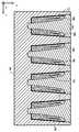
다음으로, 도 2에 의해 도시된 바와 같이, 딥(deep) 트렌치 마스크(116)가 형성되고, 도 3에 의해 도시된 바와 같이, 딥 분리 트렌치들(118)이 에칭된다. 딥 트렌치 마스크(116)는 포토레지스트 또는 하드 마스크일 수 있고, 딥 트렌치 마스크(116)는 나노-임프린트 시스템 또는 전자 빔 시스템과 같은, 포토리소그래피 장치 또는 다른 유형들의 리소그래픽 장치로 패터닝될 수 있다. 딥 트렌치 마스크(116)는 일반적으로 선형적이고 일반적으로 평행한, 일반적으로 1/4 F, 1/2 F 또는 F보다 작거나 같은 폭(120)을 갖는 노출된 영역들과, 일반적으로 3/4 F, 3/2 F, 또는 3 F보다 작거나 같은 폭(122)을 갖는 마스크된 영역들을 포함하며, 여기서 F는 딥 트렌치 마스크(116)를 패터닝하는 데에 사용되는 시스템의 분해능이다.Next, as shown by FIG. 2, a
일부 실시예들에서, 딥 트렌치 마스크(116)는 마스크를 더블 피칭하는 것에 의해 형성된다(도시 생략). 그러한 프로세스의 일 예시에서, 딥 트렌치 마스크(116)는 노출된 영역들의 모든 다른 쌍 사이의 영역들을 마스크 오프하고, 노출된 영역들의 각각에 대응하는 영역들 위에서 마스크의 측면들에 폴리-실리콘 측벽 스페이서를 형성함으로써 우선 형성된다. 그리고 초기 마스크를 제거할 수 있고 산화물과 같은 하드 마스크 재료를 남아있는 폴리-실리콘 측벽 스페이서들 위에 퇴적할 수 있고, 하드 마스크 재료를 에칭 백(etched back)하거나 화학적 기계적 평탄화(CMP)로 평탄화하여 폴리-실리콘을 노출시킬 수 있다. 다음으로, 폴리-실리콘을 선택적으로 에칭하여 도 2에 도시된 노출된 영역들 및 산화물 하드 마스크를 형성할 수 있다. 노출된 영역들의 폭(122)이 일반적으로 측벽 스페이서의 폭에 의해 결정되기 때문에, 일부 실시예들에서, 폭(122)은 F보다 작을 수 있다.In some embodiments,
도 3에 의해 도시된 바와 같이, 마스크(116)에 의해 노출된 기판(110)의 영역들을 에칭하여 딥 분리 트렌치들(118)을 형성할 수 있다. 이러한 실시예에서, 에칭은 일반적으로 이방성 건식 에칭이다. 딥 분리 트렌치들(118)은 일반적으로 Y 방향에서 옆으로 Z 방향에서 아래쪽으로 뻗어있다. 딥 분리 트렌치들(118)은 일반적으로 직사각형 또는 사다리꼴 단면을 가질 수 있고, 일부 실시예들에서는, 그것들의 단면은 일반적으로 Y 방향에서 일부 구간 동안 균일할 수 있다.As shown by FIG. 3, regions of the
다음으로 본 발명에서, 딥 트렌치 마스크(116)를 제거하고, 딥 분리 트렌치(118)를, 도 4에 의해 도시된 바와 같이, 유전체로 채운다. 딥 트렌치 마스크(116)는 노(furnace) 또는 플라즈마 에칭 챔버에서 산소와 포토레지스트를 반응시키는 것 또는 선택적으로 마스크 재료를 습식 에칭하는 것과 같이, 다양한 기술들로 제거될 수 있다. 일부 실시예들에서, 딥 트렌치 마스크(116)는 딥 분리 트렌치(118)를 채운 후에 제거된다. 다른 실시예들에서, 딥 트렌치 마스크(116)는 딥 분리 트렌치(118)를 채우기 전에 제거될 수도 있다. 예를 들어, 유전체 과잉부(overburden)가 딥 트렌치 마스크(116) 위에와 딥 분리 트렌치(118)에 모두 퇴적될 수 있고, 과잉부를 제거하는 화학적-기계적 평탄화(CMP) 동안 딥 트렌치 마스크(116)가 정지 영역(stop region)의 역할을 할 수 있다. 딥 분리 트렌치(118)는, 특히, 고밀도 플라즈마(HDP) 산화물, 스핀-온-글라스(SOG), 또는 테트라에틸오르토실리케이트(TEOS)와 같은 다양한 유전체 재료들로 부분적으로 또는 전체적으로 채워져 전기적으로 피처들을 분리시킬 수 있다. 피처들을 더 분리시키도록, 일부 실시예들에서는, 트렌치(118)를 채우기 전에 분리를 향상시키기 위해 선택된 도펀트를 딥 분리 트렌치(118)의 하부에 주입할 수 있다. 추가적으로, 딥 분리 트렌치(118)는, 막 스트레스를 완화시키고, 부착을 향상시키고, 또는 장벽 재료로 기능하는, 예를 들면 실리콘 질화물과 같은 다양한 라이너(liner) 재료들을 포함할 수 있다.Next, in the present invention, the
딥 분리 트렌치(118)를 채운 후에, 도 5에 의해 도시된 바와 같이, 셸로우 트렌치 마스크(124)가 기판(110) 상에 형성된다. 딥 트렌치 마스크(116)와 같이, 셸로우 트렌치 마스크(124)는 포토레지스트 또는 하드 마스크일 수 있고, 전술한 바와 같이, 다양한 리소그래픽 시스템들로 패터닝될 수 있다. 일부 실시예들에서, 셸로우 트렌치 마스크(124)는 마스크가 X 방향으로 1/2 피치만큼 이동된다는 것을 제외하고는 전술한 분리 트렌치 마스크(116)에 대한 것과 유사한 프로세스인 더블 피치 마스크 프로세스로 형성된 하드 마스크이다. 도시된 셸로우 트렌치 마스크(124)는 일반적으로 1/4 F, 1/2 F 또는 F보다 작거나 같은 폭을 가질 수 있는 공간(126)을 갖는 노출된 영역들과, 일반적으로 3/4 F, 3/2 F, 또는 3 F보다 작거나 같은 폭을 가질 수 있는 폭(128)을 갖는 덮인 영역들을 포함한다. 노출된 영역들은 일반적으로 선형이고, 일반적으로 평행하고, 일반적으로 딥 분리 트렌치들(118) 사이에 등간격으로 개재될 수 있다.After filling the
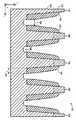
다음으로, 도 6에 의해 도시된 바와 같이, 기판(110)의 노출된 영역은 셸로우 트렌치(130)를 형성하도록 에칭된다. 셸로우 트렌치(130)는 일반적으로 선형이고, 일반적으로 평행하고, 일반적으로 Y 방향에서 옆으로, 일반적으로 Z 방향에서 아래로 뻗어있고, 따라서, 일반적으로 딥 분리 트렌치(118)에 평행할 수 있다. 이러한 실시예에서, 셸로우 트렌치(130)는 일반적으로 이방성 건식 에칭으로 형성되고 상부 도핑된 영역(112)보다 깊지만, 딥 분리 트렌치(118) 만큼 깊지는 않다. 셸로우 트렌치(130)는 상당한 구간 동안 Y 방향으로 일반적으로 균일한 일반적으로 직사각형이거나 일반적으로 사다리꼴 모양을 가질 수 있다.Next, as shown by FIG. 6, the exposed regions of the
도 7에 의해 도시된 바와 같이, 셸로우 트렌치(130)는 질화물과 같은 희생 재료로 채워질 수 있다. 이러한 실시예에서, 셸로우 트렌치(130)가 딥 분리 트렌치(118)로부터 상당량의 재료를 제거하는 일 없이 후속 단계에서 선택적으로 에칭될 수 있도록, 셸로우 트렌치(130)는 딥 분리 트렌치(118)와는 상이한 재료로 채워질 수 있다. 하지만 다른 실시예에서는, 이러한 트렌치들(118, 130)은 동일한 재료를 포함할 수 있다.As shown by FIG. 7, the
다음으로, 도 8에 의해 도시된 바와 같이, 핀 마스크(132)가 형성된다. 핀 마스크(132)는 포토레지스트로 만들어질 수 있고, 또는 하드 마스크일 수 있다. 핀 마스크(132)는 전술한 또는 다른 리소그래픽 시스템들 중 아무것으로나 패터닝될 수 있다. 이러한 실시예에서, 핀 마스크(132)는 폭(134)을 갖는 마스크된 영역과 폭(136)을 갖는 노출된 영역을 디파인(define)한다. 폭(134)은 일반적으로 F보다 작거나 같을 수 있고, 폭(136)은 일반적으로 3/2 F보다 작거나 같을 수 있다. 마스크된 영역들은 일반적으로 곧게 뻗어있고, 일반적으로 서로 평행하고, 일반적으로 딥 분리 트렌치(118) 및 셸로우 트렌치(130) 모두에 수직하고 일반적으로 X 방향으로 뻗어 있다.Next, as shown by FIG. 8, a
일부 실시예들에서, 핀 마스크(132)는 더블 피치되어 있다. 도 9에 의해 도시된 바와 같이, 측벽 스페이서(138)는, 핀 마스크(132)의 측벽에 형성될 수 있다. 측벽 스페이서(138)는 기판(110) 상에 등각 막을 퇴적시키고 등각 막을 이방성 에칭하여 수평 표면으로부터 제거함으로써 형성될 수 있다. 측벽 스페이서(138)는 후속 단계에서 핀 마스크(132)의 선택적 제거를 용이하게 하도록 핀 마스크(132)와는 상이한 재료로 만들어질 수 있다. 측벽 스페이서(138)는 일반적으로 1/4 F, 1/2 F 또는 F보다 작거나 같은 폭(140)을 가질 수 있다.In some embodiments, the
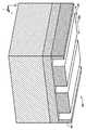
다음으로, 도 10에 의해 도시된 바와 같이, 핀 마스크(132)가 제거되고, 도 11에 의해 도시된 바와 같이, 핀 행들(142)이 형성된다. 핀 마스크(132)는 기판(110)의 다른 재료들보다 상당히 높은 속도로 핀 마스크 재료를 선택적으로 제거하는 에칭 또는 다른 프로세스로 제거될 수 있다. 각각의 노출된 측벽 스페이서들(138)은 핀 행들(142)의 상부에 일반적으로 대응하는 영역을 마스크할 수 있다. 이러한 실시예에서, 핀 행들(142)은 셸로우 트렌치(130)의 깊이 보다는 일반적으로 더 깊지만, 딥 분리 트렌치(118) 보다는 깊지 않은, 깊이(144)로 일반적으로 이방성 에칭으로 에칭된다. 핀 행들(142)은 상당한 구간 동안 X 방향으로 일반적으로 균일하게 뻗어있는 일반적으로 사다리꼴 단면을 가질 수 있다. 다른 실시예들에서, 핀 행들(142)은 일반적으로 직사각형 또는 만곡한 모양과 같은, 다른 모양을 가질 수도 있다.Next, as shown by FIG. 10, the
다음으로, 도 12에 의해 도시된 바와 같이, 스페이서(138)는 제거될 수 있고, 또는 일부 실시예들에서, 스페이서들(138)은 핀 행들(142) 상에 남겨지고 후속 단계 동안 제거될 수 있다.Next, as shown by FIG. 12, the
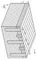
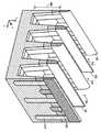
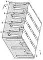
도 13 및 도 14는 핀 행들(142)의 측벽에 형성될 수 있는 (이 실시예에서 몰드로 기능하고, 지칭될 수 있는) 희생 재료(146)를 도시한다. 희생 재료(142)는 측벽 스페이서 프로세스로 형성될 수 있다. 희생 재료(142)는 도 18을 참조로 하여 후속적으로 설명된 전도과정 하에서 (예를 들면, 기체 또는 액체와 같은, 유체가 될 수 있는) 유동성으로 될 수 있는 재료로 형성될 수 있다. 처치가능한-몰드 재료의 예시들은 노에서 산소와 반응시키는 것에 의해 기체로서 기판(110)으로부터 제거될 수 있는, 탄소 및 특정 폴리머들을 포함할 수 있다. 등각 막은 상부 도핑된 영역(112)과 하부 도핑된 영역(114)을 덮으면서, 기판(110) 상에 퇴적될 수 있고, 후속적으로 이방성 에칭된다. 측벽 스페이서 에칭은 리세스(148)를 형성하도록 하부 도핑된 영역(114)의 일부를 제거할 수 있다. 리세스(148)는 일반적으로 1 F, 1/2 F, 또는 1/4 F보다 작거나 같은 폭(150)을 가질 수 있다. 후술되는 바와 같이, 리세스(148)를 형성할 때까지 측벽 스페이서 에칭을 계속하는 것은 몰드(146)로 형성된 게이트들이 서로 쇼트할 가능성을 감소시키는 것으로 생각된다. 이러한 실시예에서, 희생 재료(146)는 상부 도핑된 영역(112)의 바닥 위로 뻗고 1 F, 1/2 F, 또는 1/4 F보다 작거나 일반적으로 같을 수 있는 폭(152)을 갖는다.13 and 14 illustrate sacrificial material 146 (which may function and be referred to as a mold in this embodiment) that may be formed on the sidewalls of the
희생 재료(146)를 형성한 후에, 도 15에 의해 도시된 바와 같이, 유전체 영역(154)은 희생 재료(146) 위에 형성될 수 있다. 일부 실시예들에서, 유전체 영역(154)은 원자-층-퇴적(ALD)과 같은, 저온 프로세스로 산화물 퇴적될 수 있다. 도시된 유전체(154)는 실질적으로 또는 전체적으로 희생 재료(146)를 덮고 과잉부(156)를 포함한다.After forming the
과잉부(156)는 도 16에 의해 도시된 평탄화 단계에서 소멸된다. 기판(110)은 에칭 백, CMP, 또는 다른 프로세스들로 평탄화될 수 있다. 일부 실시예들에서, 과잉부(156)는 상부 도핑된 영역(112), 딥 분리 트렌치(118), 및 셸로우 트렌치(130)의 윗면이 노출될 때까지 제거될 수 있다. 유전체 영역(154)과 이러한 구조체들(112, 118, 130) 사이의 전이는 기판(110)을 평탄화하는 데에 사용되는 프로세스로의 종점을 트리거하는 현상을 만들 수 있다. 예를 들어, 이러한 전이는 기판(110)의 (색상 같은) 광학 특성의 변화, 기판(110)에 남기는 낭비 재료의 (에칭 챔버의 낭비 기체 또는 현탁액 pH 같은) 화학적 특성의 변화, 기판(110)의 (미끄럼 마찰 같은) 기계적 특성의 변화를 초래할 수 있다.The
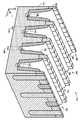
다음으로, 도 17에 의해 도시된 바와 같이, 셸로우 트렌치(130)의 재료의 적어도 일부가 제거될 수 있다. 일부 실시예들에서, 이 재료는 질화물이고, 이러한 재료들의 상당량을 잃지 않기 위해 실리콘 및 산화물에 선택적인 건식 에칭으로 제거될 수 있다. 셸로우 트렌치(130)의 적어도 일부를 제거하는 것은 희생 재료(146)의 측벽(158)으로의 통로(passage)를 열고, 이 통로는 희생 재료(146)의 제거를 용이하게 할 수 있다.Next, as shown by FIG. 17, at least a portion of the material of the
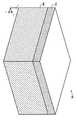
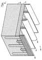
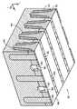
도 18에 의해 도시된 바와 같이, 희생 재료(146)는 셸로우 분리 트렌치(130)를 통한 개방 통로에 의해 제거될 수 있다. 희생 재료(146)를 제거하기 위해, 기판(110)은, 예를 들면, 플라즈마 에칭 챔버에서는 산소 플라즈마, 또는 노에서는 산소에 노출될 수 있다. 플라즈마 또는 다른 반응물은 셸로우 분리 트렌치(130)를 통해 흐르고 희생 재료(146)의 측벽(158)과, 예를 들어, 희생 재료(146)를 연소시킴으로써, 반응한다. 일부 실시예들에서, 반응의 부산물들은 예를 들어, 스팀, 일산화 탄소, 이산화 탄소, 및 셸로우 분리 트렌치(130)를 통해 역으로 흐르는 기체들 같은 기체들이다. 일부 실시예들에서, 연소는 실질적인 부분 또는 실질적으로 전체 희생 재료(146)가 연소되어 캐비티들(160)이 형성될 때까지 계속된다. 그 결과적인 캐비티들(160)은 유전체(154)에 의해 한 면 및 핀 행들(142)에 의해 다른 면이 정해진다.As shown by FIG. 18, the
캐비티들(160)의 형상이, 기판(110)의 다른 부분 없이 캐비티들(160)을 도시하는 도 19에 의해 도시되었다. 각각의 캐비티들(160)은 2개의 일반적으로 반사적인 대칭이고, 일반적으로 선형이고, 일반적으로 평행한 공간들(162, 164) 및 복수의 트렌치 세그먼트들(166)을 포함한다. 도시된 트렌치 세그먼트들(166)은 공간들(162, 164)의 윗부분에 배치되고 공간들(162, 164)을 서로 결합한다. 인접한 캐비티들(160)은 실질적으로 또는 전체적으로 유전체(154)에 의해 서로 분리될 수 있다(도 18).The shape of the
다음으로, 도 20에 의해 도시된 바와 같이, 게이트 유전체(166)는 캐비티들들(160) 내에서 형성될 수 있다. 게이트 유전체(166)는 예를 들면, CVD로 퇴적될 수도 있고, 또는 기판(110)을 산소에 노출시킴으로써 성장할 수도 있다. 도시된 실시예에서, 게이트 유전체(166)는 기판(110)의 실리콘 부분을 산소와 반응시킴으로써 성장하고, 따라서 게이트 유전체(166)는 셸로우 트렌치(130)의 표면을 포함하여, 핀 행들(142)의 노출된 표면 상에 배치된다. 게이트 유전체(166)를 형성하도록 반응하는 산소 또는 다른 화학물들은 트렌치 세그먼트들(166)을 통해 캐비티들(160)로 흘러들어가고 선형 공간들(162, 164)(도 19) 내에서 표면들과 반응한다. 다양한 실시예들에서, 게이트 유전체(166)는 산소, 산질화물, 하프늄-기반 고-K 유전체, 또는 다른 적절한 재료들을 포함하는 다양한 재료들로부터 만들어질 수 있다.Next, as shown by FIG. 20,
게이트 유전체(166)가 형성되면, 도 21 내지 도 23에 의해 도시된 바와 같이, 게이트 재료는 게이트들(168)을 형성하도록 캐비티들(166) 내에서 퇴적될 수 있다. 도시된 게이트들(168)은 티타늄 질화물 또는 다른 적절한 전도성 재료들을 퇴적시킴으로써 형성될 수 있다. 게이트 재료는 기상 반응물에 의해 기판(110)으로 그리고 캐비티들(166) 안으로 전달될 수 있다. 반응물은 셸로우 트렌치(130)를 통해 캐비티들(166)로 흘러들어갈 수 있고 캐비티들(166)의 표면 상에서 반응할 수 있다. 일부 실시예들에서, 게이트 재료는 캐비티들(166)이 채워지기 전에 셸로우 트렌치(130)를 닫아서, 그것으로 인해 공간들(170)을 남긴다. 게이트 재료의 과잉부는 기판(110)의 표면 상에서 형성될 수 있고, 과잉부는 습식 에칭, 건식 에칭, 또는 CMP 프로세스로 제거될 수 있다.Once the
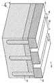
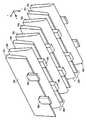
도 24는 전술한 프로세스로 형성된 트랜지스터(171)의 일례의 분해된, 투시도이다. 그러나, 본 기술은 트랜지스터로만 제한되지 않고, 캐패시터들 또는 플로팅-게이트 트랜지스터들과 같은, 다른 디바이스들을 형성하는 데에도 사용될 수 있음을 유의하여야 한다. 도시된 트랜지스터(171)는 핀(172), 게이트 유전체(166), 및 게이트(168)를 포함한다. 도시된 핀(172)은 셸로우 트렌치(130)에 대응하는 일반적으로 U-형상 슬롯(178)에 의해 분리된 2개의 레그들(leg)(174, 176)을 포함한다. 핀(172)의 말단부는 상부 도핑된 영역(112)으로 만들어지고, 핀(172)의 하단 부분은 하부 도핑된 영역(114)으로 만들어 진다. 에지들(180, 182)은 일반적으로 딥 분리 트렌치들(118)에 의해 디파인되고 핀(172)의 측면들(184, 185)보다 더 길 수 있다. 도시된 게이트(166)는 측면들(184, 185) 및 슬롯(178)의 표면에 모두 인접하게 배치된다.24 is an exploded, perspective view of an example of a transistor 171 formed in the process described above. However, it should be noted that the present technology is not limited to transistors, but may also be used to form other devices, such as capacitors or floating-gate transistors. The illustrated transistor 171 includes a
도시된 실시예에서, 게이트(168)는 2개의 측면 게이트들(186, 188)과 상부 게이트(190)를 포함한다. 2개의 측면 게이트들(186, 188)은 일반적으로 반사적 대칭이고 둘 다 일반적으로 실질적인 구간 동안 일반적으로 균일한 단면을 갖고 X 방향으로 일반적으로 뻗는다. 측면 게이트들(186, 188)의 형상은 공간들(170)을 제외한 희생 재료(146)의 형상에 일반적으로 상보적이다. 도시된 상부 게이트(190)는 Y 방향에서 일반적으로 균일한 단면을 갖고 측면 게이트들(186, 188)을 서로 결합한다. 상부 게이트(190)는, 공간이 없고, 일반적으로 고체일 수 있고, 또는 일부 실시예들에서, 상부 게이트(190)는 또한 공간을 포함할 수 있다. 측면 게이트(186)는 핀(172)의 측면(185)에 적어도 부분적으로 인접하게 배치되고, 상부 게이트(190)는 슬롯(178)내에서 적어도 부분적으로 배치되고, 측면 게이트(188)는 핀(172)의 측면(184)에 적어도 부분적으로 인접하게 배치된다. 도시된 트랜지스터(171)는, 게이트(168)가 핀(172)의 2개의 측면과 상부 부분에 인접하게 배치되기 때문에, 3-게이트 트랜지스터로서 특성을 가질 수 있다.In the illustrated embodiment, the
동작시, 2개의 레그들(174, 176)은 소스 및 드레인으로 기능할 수 있고, 트랜지스터(171)는 게이트(168)의 전압에 따라 소스와 드레인 사이의 전류의 흐름을 선택적으로 제어할 수 있다. 도시된 트랜지스터(171)는 3개의 채널을 포함한다: 화살표(192)로 도시된 일반적으로 수평의 채널 및 화살표(194)로 도시된 2개의 일반적으로 수직의 채널들. 일반적으로 수평의 채널(192)은 상부 게이트(190)로 부터 발산되는 전기장에 의해 설립될 수 있고, 일반적으로 수직의 채널들(194)은 2개의 측면 게이트들(186, 188)로부터 발산되는 전기장에 의해 설립될 수 있다.In operation, the two
본 발명이 다양한 수정 및 대안적인 형태의 여지가 있을지라도, 특정한 실시예들이 도면들의 예시의 방법에 의해 도시되었고 본원에서 구체적으로 설명되었다. 그러나, 본 발명이 개시된 특정한 형태로 제한되도록 의도되지 않음을 이해하여야만 한다. 그것보다는, 본 발명은 하기의 첨부된 청구범위에 의해 정의된 본 발명의 사상 및 범주 내에 해당되는 모든 수정들, 균등항들, 및 대안책들을 포함하여야 한다.Although the invention is susceptible to various modifications and alternative forms, specific embodiments have been shown by way of example of the drawings and are described in detail herein. However, it should be understood that the invention is not intended to be limited to the particular forms disclosed. Rather, the present invention should include all modifications, equivalents, and alternatives falling within the spirit and scope of the invention as defined by the appended claims below.
Claims (25)
Translated fromKorean상기 반도체 핀에 인접한 희생 재료를 형성하는 단계와,
상기 희생 재료를 유전체 재료로 덮는 단계와,
상기 유전체 재료 아래로부터 상기 희생 재료를 제거함으로써 캐비티를 형성하는 단계와,
상기 캐비티에 게이트를 형성하는 단계
를 포함하는 방법.Forming a semiconductor fin,
Forming a sacrificial material adjacent the semiconductor fins;
Covering said sacrificial material with a dielectric material;
Forming a cavity by removing said sacrificial material from below said dielectric material;
Forming a gate in the cavity
How to include.
상기 희생 재료를 형성하는 단계는 상기 반도체 핀에 인접한 측벽 스페이서를 형성하는 단계를 포함하는 방법.The method of claim 1,
Forming the sacrificial material comprises forming sidewall spacers adjacent the semiconductor fins.
상기 측벽 스페이서를 형성하는 단계는 탄소-측벽 스페이서를 형성하는 단계를 포함하는 방법.The method of claim 2,
Forming the sidewall spacers comprises forming a carbon-sidewall spacer.
상기 희생 재료를 제거하는 단계는,
몰드의 적어도 일부를 노출시키는 단계와,
상기 희생 재료의 적어도 일부를 유체로 전환하는 단계
를 포함하는 방법.The method of claim 1,
Removing the sacrificial material,
Exposing at least a portion of the mold,
Converting at least a portion of the sacrificial material into a fluid
How to include.
상기 희생 재료의 적어도 일부를 노출시키는 단계는 상기 희생 재료 위에 배치된 상기 유전체 재료의 전부가 아닌 일부를 화학적-기계적 평탄화로 제거하는 단계를 포함하는 방법.The method of claim 4, wherein
Exposing at least a portion of the sacrificial material comprises removing, but not all, a portion of the dielectric material disposed over the sacrificial material by chemical-mechanical planarization.
상기 희생 재료의 적어도 일부를 노출시키는 단계는 상기 반도체 핀을 가로지르는 상기 희생 재료의 일부가 적어도 부분적으로 노출될 때까지 유전체 재료를 제거하는 단계를 포함하는 방법.The method of claim 4, wherein
Exposing at least a portion of the sacrificial material comprises removing a dielectric material until at least partially exposing a portion of the sacrificial material across the semiconductor fin.
상기 희생 재료의 적어도 일부를 상기 유체로 전환하는 단계는 상기 몰드의 적어도 상당한 부분을 연소시키는 단계를 포함하는 방법.The method of claim 4, wherein
Converting at least a portion of the sacrificial material into the fluid comprises burning at least a substantial portion of the mold.
상기 캐비티를 형성하는 단계는,
상기 반도체 핀의 각 측면 상에 일반적으로 선형인 공간들을 형성하는 단계와,
상기 일반적으로 선형인 공간들 사이에서 뻗어있는 트렌치 세그먼트들을 형성하는 단계
를 포함하는 방법.The method of claim 1,
Forming the cavity,
Forming generally linear spaces on each side of the semiconductor fin;
Forming trench segments extending between the generally linear spaces
How to include.
상기 캐비티에 상기 게이트를 형성하는 단계는 반응물 기체를 상기 캐비티 내의 복수의 개구부들로 흘림으로써 상기 반도체 핀의 적어도 3개의 측면을 가로지르는 게이트를 형성하는 단계를 포함하는 방법.The method of claim 1,
Forming the gate in the cavity comprises forming a gate across at least three sides of the semiconductor fin by flowing a reactant gas into the plurality of openings in the cavity.
상기 핀 행에 인접하게 배치된 공동(hollow) 게이트
를 포함하는 디바이스.A pin row comprising a plurality of pin field-effect transistors,
Hollow gate disposed adjacent to the fin row
Device comprising a.
상기 게이트는 상기 복수의 핀 전계-효과 트랜지스터들의 말단부를 통해 지나가는 복수의 트렌치 세그먼트들을 포함하는 디바이스.The method of claim 10,
The gate includes a plurality of trench segments passing through an end of the plurality of fin field-effect transistors.
상기 복수의 핀 전계-효과 트랜지스터들 중의 각각의 핀 전계-효과 트랜지스터는 3개의 채널들을 포함하는 디바이스.The method of claim 10,
Wherein each pin field-effect transistor of the plurality of pin field-effect transistors comprises three channels.
상기 복수의 핀 전계-효과 트랜지스터들 중의 각각의 핀 전계-효과 트랜지스터는 일반적으로 U-형상의 말단부를 포함하는 디바이스.The method of claim 10,
Each pin field-effect transistor of the plurality of pin field-effect transistors generally comprises a U-shaped end portion.
상기 복수의 핀 전계-효과 트랜지스터들 중의 각각의 핀 전계-효과 트랜지스터의 핀 폭은 포토리소그래픽-분해능 한계보다 작은 디바이스.The method of claim 10,
Wherein the fin width of each fin field-effect transistor of said plurality of fin field-effect transistors is less than a photolithographic-resolution limit.
상기 희생 재료는 무정형 탄소, 포토레지스트, 또는 둘 다를 포함하는 방법.16. The method of claim 15,
The sacrificial material comprises amorphous carbon, photoresist, or both.
상기 희생 재료는 상기 핀의 일 측면에 배치된 제1 측벽 스페이서 및 상기 핀의 다른 측면에 배치된 제2 측벽 스페이서를 포함하는 방법.16. The method of claim 15,
The sacrificial material comprises a first sidewall spacer disposed on one side of the fin and a second sidewall spacer disposed on the other side of the fin.
상기 희생 재료는 상기 핀으로부터 뻗은 2개의 레그들 사이에 배치된 트렌치 세그먼트를 포함하는 방법.16. The method of claim 15,
The sacrificial material comprises a trench segment disposed between two legs extending from the pin.
상기 제1 측벽 스페이서는 상기 트렌치 세그먼트에 의해 상기 제2 측벽 스페이서와 결합되는 방법.The method of claim 18,
And the first sidewall spacer is coupled with the second sidewall spacer by the trench segment.
상기 희생 재료를 기체로 전환함으로써 상기 핀에 인접한 게이트를 디파인하는 단계를 포함하는 방법.16. The method of claim 15,
Defining a gate adjacent the fin by converting the sacrificial material into a gas.
각각이 인접한 3-게이트 트랜지스터들의 상기 측면 게이트들 사이에 배치된 복수의 유전체 부재들 - 상기 유전체 부재들은 상기 측면 게이트들보다 더 깊이 리세스들로 뻗어있음 -
을 포함하는 디바이스.A plurality of three-gate transistors each comprising an upper gate and two side gates,
A plurality of dielectric members each disposed between the side gates of adjacent three-gate transistors, the dielectric members extending into recesses deeper than the side gates;
Device comprising a.
상기 리세스들은 측벽-스페이서-오버-에칭 리세스들인 디바이스.The method of claim 21,
And the recesses are sidewall-spacer-over-etching recesses.
상기 리세스들은 포토리소그래피-분해능 한계보다 좁은 디바이스.The method of claim 21,
Wherein the recesses are narrower than the photolithography-resolution limit.
상기 상부 게이트 또는 상기 2개의 측면 게이트들 중 적어도 하나는 캐비티 내에 형성되는 디바이스.The method of claim 21,
At least one of the top gate or the two side gates is formed in a cavity.
상기 상부 게이트 및 상기 2개의 측면 게이트들의 각각은 캐비티 내에 형성되는 디바이스.25. The method of claim 24,
And the top gate and each of the two side gates are formed in a cavity.
Applications Claiming Priority (2)
| Application Number | Priority Date | Filing Date | Title |
|---|---|---|---|
| US12/043,813 | 2008-03-06 | ||
| US12/043,813US7915659B2 (en) | 2008-03-06 | 2008-03-06 | Devices with cavity-defined gates and methods of making the same |
Publications (2)
| Publication Number | Publication Date |
|---|---|
| KR20100131478Atrue KR20100131478A (en) | 2010-12-15 |
| KR101547375B1 KR101547375B1 (en) | 2015-08-25 |
Family
ID=40551557
Family Applications (1)
| Application Number | Title | Priority Date | Filing Date |
|---|---|---|---|
| KR1020107022401AActiveKR101547375B1 (en) | 2008-03-06 | 2009-02-24 | Devices with cavity-defined gates and methods of making the same |
Country Status (6)
| Country | Link |
|---|---|
| US (3) | US7915659B2 (en) |
| JP (1) | JP5360507B2 (en) |
| KR (1) | KR101547375B1 (en) |
| CN (1) | CN101960572B (en) |
| TW (1) | TWI430371B (en) |
| WO (1) | WO2009111225A1 (en) |
Cited By (1)
| Publication number | Priority date | Publication date | Assignee | Title |
|---|---|---|---|---|
| KR20160138592A (en)* | 2012-09-19 | 2016-12-05 | 인텔 코포레이션 | Gate contact structure over active gate and method to fabricate same |
Families Citing this family (35)
| Publication number | Priority date | Publication date | Assignee | Title |
|---|---|---|---|---|
| US7898857B2 (en) | 2008-03-20 | 2011-03-01 | Micron Technology, Inc. | Memory structure having volatile and non-volatile memory portions |
| US8546876B2 (en) | 2008-03-20 | 2013-10-01 | Micron Technology, Inc. | Systems and devices including multi-transistor cells and methods of using, making, and operating the same |
| US7969776B2 (en) | 2008-04-03 | 2011-06-28 | Micron Technology, Inc. | Data cells with drivers and methods of making and operating the same |
| KR20090105700A (en)* | 2008-04-03 | 2009-10-07 | 주식회사 하이닉스반도체 | Manufacturing method of semiconductor device |
| US8704375B2 (en)* | 2009-02-04 | 2014-04-22 | Taiwan Semiconductor Manufacturing Company, Ltd. | Barrier structures and methods for through substrate vias |
| JP5718585B2 (en)* | 2010-05-19 | 2015-05-13 | ピーエスフォー ルクスコ エスエイアールエルPS4 Luxco S.a.r.l. | Semiconductor device, manufacturing method thereof, and data processing system |
| DE102010030760B4 (en)* | 2010-06-30 | 2014-07-24 | Globalfoundries Dresden Module One Limited Liability Company & Co. Kg | Semiconductor device with via contacts with a stress relaxation mechanism and method of making the same |
| US8334196B2 (en) | 2010-11-01 | 2012-12-18 | Micron Technology, Inc. | Methods of forming conductive contacts in the fabrication of integrated circuitry |
| US9553193B2 (en) | 2010-11-19 | 2017-01-24 | Micron Technology, Inc. | Double gated fin transistors and methods of fabricating and operating the same |
| US8294511B2 (en) | 2010-11-19 | 2012-10-23 | Micron Technology, Inc. | Vertically stacked fin transistors and methods of fabricating and operating the same |
| US8293602B2 (en) | 2010-11-19 | 2012-10-23 | Micron Technology, Inc. | Method of fabricating a finFET having cross-hair cells |
| US8921899B2 (en) | 2010-11-19 | 2014-12-30 | Micron Technology, Inc. | Double gated 4F2 dram CHC cell and methods of fabricating the same |
| US8969154B2 (en)* | 2011-08-23 | 2015-03-03 | Micron Technology, Inc. | Methods for fabricating semiconductor device structures and arrays of vertical transistor devices |
| JP5646416B2 (en)* | 2011-09-01 | 2014-12-24 | 株式会社東芝 | Manufacturing method of semiconductor device |
| KR101823105B1 (en) | 2012-03-19 | 2018-01-30 | 삼성전자주식회사 | Method for fabricating field effect transistor |
| CN103531467B (en)* | 2012-07-02 | 2016-08-03 | 中芯国际集成电路制造(上海)有限公司 | Semiconductor device and forming method thereof |
| US20140103452A1 (en)* | 2012-10-15 | 2014-04-17 | Marvell World Trade Ltd. | Isolation components for transistors formed on fin features of semiconductor substrates |
| US9263585B2 (en)* | 2012-10-30 | 2016-02-16 | Globalfoundries Inc. | Methods of forming enhanced mobility channel regions on 3D semiconductor devices, and devices comprising same |
| US8946050B2 (en)* | 2012-10-30 | 2015-02-03 | Globalfoundries Inc. | Double trench well formation in SRAM cells |
| CN103855026B (en)* | 2012-12-06 | 2017-04-19 | 中国科学院微电子研究所 | Finfet and manufacturing method thereof |
| CN103928334B (en)* | 2013-01-15 | 2017-06-16 | 中国科学院微电子研究所 | Semiconductor device and method for manufacturing the same |
| JP2014222682A (en)* | 2013-05-13 | 2014-11-27 | ピーエスフォー ルクスコ エスエイアールエルPS4 Luxco S.a.r.l. | Semiconductor device and method of manufacturing the same |
| US9343320B2 (en) | 2013-12-06 | 2016-05-17 | Globalfoundries Inc. | Pattern factor dependency alleviation for eDRAM and logic devices with disposable fill to ease deep trench integration with fins |
| US9871121B2 (en) | 2014-03-10 | 2018-01-16 | Qualcomm Incorporated | Semiconductor device having a gap defined therein |
| TWI642110B (en)* | 2014-12-03 | 2018-11-21 | 聯華電子股份有限公司 | Semiconductor component and manufacturing method thereof |
| US9466602B1 (en) | 2015-06-15 | 2016-10-11 | International Business Machines Corporation | Embedded dynamic random access memory field effect transistor device |
| US9553194B1 (en)* | 2015-07-29 | 2017-01-24 | Globalfoundries Inc. | Method for improved fin profile |
| CN106611787A (en)* | 2015-10-26 | 2017-05-03 | 联华电子股份有限公司 | Semiconductor structure and manufacturing method thereof |
| US10504821B2 (en)* | 2016-01-29 | 2019-12-10 | United Microelectronics Corp. | Through-silicon via structure |
| US9691864B1 (en)* | 2016-05-13 | 2017-06-27 | Infineon Technologies Americas Corp. | Semiconductor device having a cavity and method for manufacturing thereof |
| US10157745B2 (en)* | 2016-06-29 | 2018-12-18 | International Business Machines Corporation | High aspect ratio gates |
| US9934970B1 (en)* | 2017-01-11 | 2018-04-03 | International Business Machines Corporation | Self aligned pattern formation post spacer etchback in tight pitch configurations |
| US10770571B2 (en)* | 2018-09-19 | 2020-09-08 | Taiwan Semiconductor Manufacturing Co., Ltd. | FinFET with dummy fins and methods of making the same |
| US20220231023A1 (en)* | 2021-01-15 | 2022-07-21 | Taiwan Semiconductor Manufacturing Co., Ltd. | Finfet device and method |
| CN118738121A (en)* | 2024-04-15 | 2024-10-01 | 华南师范大学 | Based on multi-region gate single-channel microcavity transistor, optoelectronic full logic gate device, control method and circuit |
Family Cites Families (108)
| Publication number | Priority date | Publication date | Assignee | Title |
|---|---|---|---|---|
| US3885861A (en) | 1972-10-02 | 1975-05-27 | Hughes Aircraft Co | Liquid crystal digital reticle |
| US5196910A (en) | 1987-04-24 | 1993-03-23 | Hitachi, Ltd. | Semiconductor memory device with recessed array region |
| US5160987A (en) | 1989-10-26 | 1992-11-03 | International Business Machines Corporation | Three-dimensional semiconductor structures formed from planar layers |
| US5109256A (en) | 1990-08-17 | 1992-04-28 | National Semiconductor Corporation | Schottky barrier diodes and Schottky barrier diode-clamped transistors and method of fabrication |
| KR930005234B1 (en) | 1990-09-13 | 1993-06-16 | 금성일렉트론주식회사 | Cell manufacture method of fin-stack cell |
| US6791131B1 (en) | 1993-04-02 | 2004-09-14 | Micron Technology, Inc. | Method for forming a storage cell capacitor compatible with high dielectric constant materials |
| US5864181A (en) | 1993-09-15 | 1999-01-26 | Micron Technology, Inc. | Bi-level digit line architecture for high density DRAMs |
| JPH07263576A (en) | 1994-03-25 | 1995-10-13 | Hitachi Ltd | Semiconductor integrated circuit device and manufacturing method thereof |
| US6831322B2 (en) | 1995-06-05 | 2004-12-14 | Fujitsu Limited | Semiconductor memory device and method for fabricating the same |
| JP3853406B2 (en) | 1995-10-27 | 2006-12-06 | エルピーダメモリ株式会社 | Semiconductor integrated circuit device and method for manufacturing the same |
| US6043562A (en) | 1996-01-26 | 2000-03-28 | Micron Technology, Inc. | Digit line architecture for dynamic memory |
| WO1997028532A1 (en) | 1996-02-01 | 1997-08-07 | Micron Technology, Inc. | Digit line architecture for dynamic memory |
| US5688709A (en) | 1996-02-14 | 1997-11-18 | Lsi Logic Corporation | Method for forming composite trench-fin capacitors for DRAMS |
| US5793033A (en) | 1996-03-29 | 1998-08-11 | Metanetics Corporation | Portable data collection device with viewing assembly |
| US7064376B2 (en) | 1996-05-24 | 2006-06-20 | Jeng-Jye Shau | High performance embedded semiconductor memory devices with multiple dimension first-level bit-lines |
| US5821513A (en) | 1996-06-26 | 1998-10-13 | Telxon Corporation | Shopping cart mounted portable data collection device with tethered dataform reader |
| US6285045B1 (en) | 1996-07-10 | 2001-09-04 | Fujitsu Limited | Semiconductor device with self-aligned contact and its manufacture |
| JP3941133B2 (en) | 1996-07-18 | 2007-07-04 | 富士通株式会社 | Semiconductor device and manufacturing method thereof |
| US6072209A (en) | 1997-07-08 | 2000-06-06 | Micro Technology, Inc. | Four F2 folded bit line DRAM cell structure having buried bit and word lines |
| US5925918A (en) | 1997-07-30 | 1999-07-20 | Micron, Technology, Inc. | Gate stack with improved sidewall integrity |
| US6097212A (en) | 1997-10-09 | 2000-08-01 | Lattice Semiconductor Corporation | Variable grain architecture for FPGA integrated circuits |
| US6130551A (en) | 1998-01-19 | 2000-10-10 | Vantis Corporation | Synthesis-friendly FPGA architecture with variable length and variable timing interconnect |
| US6137128A (en) | 1998-06-09 | 2000-10-24 | International Business Machines Corporation | Self-isolated and self-aligned 4F-square vertical fet-trench dram cells |
| US5858829A (en) | 1998-06-29 | 1999-01-12 | Vanguard International Semiconductor Corporation | Method for fabricating dynamic random access memory (DRAM) cells with minimum active cell areas using sidewall-spacer bit lines |
| TW388125B (en) | 1998-08-19 | 2000-04-21 | Vanguard Int Semiconduct Corp | Method for fabricating dynamic random access memory (DRAM) cells with minimum active cell areas |
| DE19842704C2 (en) | 1998-09-17 | 2002-03-28 | Infineon Technologies Ag | Manufacturing process for a capacitor with a high epsilon dielectric or a ferroelectric according to the fin stack principle using a negative mold |
| TW380316B (en) | 1998-10-15 | 2000-01-21 | Worldwide Semiconductor Mfg | Manufacturing method for fin-trench-structure capacitor of DRAM |
| US6100129A (en) | 1998-11-09 | 2000-08-08 | Worldwide Semiconductor Manufacturing Corporation | Method for making fin-trench structured DRAM capacitor |
| US6426175B2 (en) | 1999-02-22 | 2002-07-30 | International Business Machines Corporation | Fabrication of a high density long channel DRAM gate with or without a grooved gate |
| US6258559B1 (en)* | 1999-03-22 | 2001-07-10 | Zymogenetics, Inc. | Method for producing proteins in transformed Pichia |
| KR100325472B1 (en) | 1999-04-15 | 2002-03-04 | 박종섭 | Manufacturing Method of DRAM Memory Cells |
| JP4074051B2 (en) | 1999-08-31 | 2008-04-09 | 株式会社東芝 | Semiconductor substrate and manufacturing method thereof |
| US6282113B1 (en) | 1999-09-29 | 2001-08-28 | International Business Machines Corporation | Four F-squared gapless dual layer bitline DRAM array architecture |
| DE19946719A1 (en) | 1999-09-29 | 2001-04-19 | Infineon Technologies Ag | Trench capacitor used in the production of DRAM storage cells has a conducting contact layer between the substrate and the conducting trench filling in the trench above the insulating collar |
| JP3457236B2 (en) | 1999-11-05 | 2003-10-14 | 茂徳科技股▲ふん▼有限公司 | Method of manufacturing deep trench capacitor storage electrode |
| WO2001061738A1 (en) | 2000-02-15 | 2001-08-23 | Steag Cvd Systems Ltd. | Dram capacitor with ultra-thin nitride layer |
| US6391753B1 (en)* | 2000-06-20 | 2002-05-21 | Advanced Micro Devices, Inc. | Process for forming gate conductors |
| JP3983960B2 (en) | 2000-07-14 | 2007-09-26 | 株式会社ルネサステクノロジ | Manufacturing method of semiconductor integrated circuit device and semiconductor integrated circuit device |
| KR100466689B1 (en) | 2000-08-28 | 2005-01-24 | 인터내셔널 비지네스 머신즈 코포레이션 | Compact dual-port dram architecture system and method for making same |
| US6509226B1 (en) | 2000-09-27 | 2003-01-21 | International Business Machines Corporation | Process for protecting array top oxide |
| US6967147B1 (en) | 2000-11-16 | 2005-11-22 | Infineon Technologies Ag | Nitrogen implantation using a shadow effect to control gate oxide thickness in DRAM semiconductor |
| US6258659B1 (en) | 2000-11-29 | 2001-07-10 | International Business Machines Corporation | Embedded vertical DRAM cells and dual workfunction logic gates |
| US6576944B2 (en) | 2000-12-14 | 2003-06-10 | Infineon Technologies Ag | Self-aligned nitride pattern for improved process window |
| CA2340985A1 (en) | 2001-03-14 | 2002-09-14 | Atmos Corporation | Interleaved wordline architecture |
| US6809368B2 (en) | 2001-04-11 | 2004-10-26 | International Business Machines Corporation | TTO nitride liner for improved collar protection and TTO reliability |
| TW502453B (en)* | 2001-09-06 | 2002-09-11 | Winbond Electronics Corp | MOSFET and the manufacturing method thereof |
| US7190060B1 (en) | 2002-01-09 | 2007-03-13 | Bridge Semiconductor Corporation | Three-dimensional stacked semiconductor package device with bent and flat leads and method of making same |
| US7019353B2 (en) | 2002-07-26 | 2006-03-28 | Micron Technology, Inc. | Three dimensional flash cell |
| US6605514B1 (en) | 2002-07-31 | 2003-08-12 | Advanced Micro Devices, Inc. | Planar finFET patterning using amorphous carbon |
| US6865100B2 (en) | 2002-08-12 | 2005-03-08 | Micron Technology, Inc. | 6F2 architecture ROM embedded DRAM |
| US7358121B2 (en)* | 2002-08-23 | 2008-04-15 | Intel Corporation | Tri-gate devices and methods of fabrication |
| US6927462B2 (en) | 2002-08-28 | 2005-08-09 | Infineon Technologes Richmond, Lp | Method of forming a gate contact in a semiconductor device |
| US6670682B1 (en) | 2002-08-29 | 2003-12-30 | Micron Technology, Inc. | Multilayered doped conductor |
| KR100481209B1 (en)* | 2002-10-01 | 2005-04-08 | 삼성전자주식회사 | MOS Transistor having multiple channels and method of manufacturing the same |
| DE10248722A1 (en) | 2002-10-18 | 2004-05-06 | Infineon Technologies Ag | Integrated circuit arrangement with capacitor and manufacturing process |
| JP3983167B2 (en)* | 2002-12-26 | 2007-09-26 | 華邦電子股▲ふん▼有限公司 | Method for manufacturing metal oxide semiconductor field effect transistor |
| DE10302128B3 (en) | 2003-01-21 | 2004-09-09 | Infineon Technologies Ag | Buffer amplifier system for buffer storage of signals runs several DRAM chips in parallel and has two output buffer amplifiers in parallel feeding reference and signal networks with capacitors and DRAMs |
| US6845033B2 (en) | 2003-03-05 | 2005-01-18 | International Business Machines Corporation | Structure and system-on-chip integration of a two-transistor and two-capacitor memory cell for trench technology |
| JP2004281782A (en) | 2003-03-17 | 2004-10-07 | Toshiba Corp | Semiconductor device and manufacturing method thereof |
| US6794254B1 (en) | 2003-05-15 | 2004-09-21 | Taiwan Semiconductor Manufacturing Company | Embedded dual-port DRAM process |
| US7099216B2 (en) | 2003-09-05 | 2006-08-29 | International Business Machines Corporation | Single cycle read/write/writeback pipeline, full-wordline I/O DRAM architecture with enhanced write and single ended sensing |
| US6844591B1 (en) | 2003-09-17 | 2005-01-18 | Micron Technology, Inc. | Method of forming DRAM access transistors |
| DE10361695B3 (en) | 2003-12-30 | 2005-02-03 | Infineon Technologies Ag | Transistor structure for dynamic random-access memory cell has recess structure between source/drain regions and vertical gate electrode enclosing active region on at least 2 sides |
| US6998666B2 (en) | 2004-01-09 | 2006-02-14 | International Business Machines Corporation | Nitrided STI liner oxide for reduced corner device impact on vertical device performance |
| DE102004006520B4 (en) | 2004-02-10 | 2010-05-12 | Qimonda Ag | Method for producing a DRAM memory cell arrangement with trench capacitors and ridge field effect transistors (FinFET) and DRAM memory cell arrangement |
| DE102004021052B3 (en) | 2004-04-29 | 2005-12-29 | Infineon Technologies Ag | Method for fabricating trench DRAM memory cells and trench DRAM memory cell array with curved channel bridge field effect transistors (CFET) |
| KR100605104B1 (en)* | 2004-05-04 | 2006-07-26 | 삼성전자주식회사 | Fin-Pet device and its manufacturing method |
| US7098105B2 (en) | 2004-05-26 | 2006-08-29 | Micron Technology, Inc. | Methods for forming semiconductor structures |
| JP4675585B2 (en)* | 2004-06-22 | 2011-04-27 | シャープ株式会社 | Field effect transistor |
| US7132333B2 (en) | 2004-09-10 | 2006-11-07 | Infineon Technologies Ag | Transistor, memory cell array and method of manufacturing a transistor |
| DE102004031385B4 (en) | 2004-06-29 | 2010-12-09 | Qimonda Ag | A method of fabricating ridge field effect transistors in a DRAM memory cell array, curved channel field effect transistors, and DRAM memory cell array |
| JP2006054431A (en) | 2004-06-29 | 2006-02-23 | Infineon Technologies Ag | Transistor, memory cell array, and transistor manufacturing method |
| US7442976B2 (en)* | 2004-09-01 | 2008-10-28 | Micron Technology, Inc. | DRAM cells with vertical transistors |
| DE102004043857B3 (en) | 2004-09-10 | 2006-03-30 | Infineon Technologies Ag | DRAM cell pair and DRAM memory cell array with stack and trench memory cells, and method of fabricating a DRAM memory cell array |
| DE102004043858A1 (en) | 2004-09-10 | 2006-03-16 | Infineon Technologies Ag | Method for producing a memory cell, a memory cell arrangement and memory cell arrangement |
| KR100585161B1 (en) | 2004-10-02 | 2006-05-30 | 삼성전자주식회사 | Multichannel transistor device manufacturing method and device |
| US7476920B2 (en) | 2004-12-15 | 2009-01-13 | Infineon Technologies Ag | 6F2 access transistor arrangement and semiconductor memory device |
| US7254074B2 (en) | 2005-03-07 | 2007-08-07 | Micron Technology, Inc. | Open digit line array architecture for a memory array |
| KR100691006B1 (en)* | 2005-04-29 | 2007-03-09 | 주식회사 하이닉스반도체 | Structure of Cell Transistor of Memory Device and Manufacturing Method Thereof |
| KR100608377B1 (en)* | 2005-05-02 | 2006-08-08 | 주식회사 하이닉스반도체 | Cell transistor manufacturing method of memory device |
| US7316953B2 (en) | 2005-05-31 | 2008-01-08 | Nanya Technology Corporation | Method for forming a recessed gate with word lines |
| KR100608380B1 (en) | 2005-06-01 | 2006-08-08 | 주식회사 하이닉스반도체 | Transistor of memory device and method for fabricating the same |
| US7282401B2 (en) | 2005-07-08 | 2007-10-16 | Micron Technology, Inc. | Method and apparatus for a self-aligned recessed access device (RAD) transistor gate |
| US7776715B2 (en) | 2005-07-26 | 2010-08-17 | Micron Technology, Inc. | Reverse construction memory cell |
| US7151023B1 (en) | 2005-08-01 | 2006-12-19 | International Business Machines Corporation | Metal gate MOSFET by full semiconductor metal alloy conversion |
| US20070058468A1 (en) | 2005-09-12 | 2007-03-15 | Promos Technologies Pte.Ltd. Singapore | Shielded bitline architecture for dynamic random access memory (DRAM) arrays |
| KR100663366B1 (en) | 2005-10-26 | 2007-01-02 | 삼성전자주식회사 | Flash memory device manufacturing method having self-aligned floating gate and related devices |
| KR100653712B1 (en) | 2005-11-14 | 2006-12-05 | 삼성전자주식회사 | Semiconductor devices in which an isolation layer having a top surface substantially the same as an active region in a fin FET is disposed and methods of forming the same |
| US7402856B2 (en) | 2005-12-09 | 2008-07-22 | Intel Corporation | Non-planar microelectronic device having isolation element to mitigate fringe effects and method to fabricate same |
| US8716772B2 (en) | 2005-12-28 | 2014-05-06 | Micron Technology, Inc. | DRAM cell design with folded digitline sense amplifier |
| KR100734304B1 (en) | 2006-01-16 | 2007-07-02 | 삼성전자주식회사 | Manufacturing method of transistor |
| KR100720238B1 (en) | 2006-01-23 | 2007-05-23 | 주식회사 하이닉스반도체 | Semiconductor element and manufacturing method thereof |
| US20070176253A1 (en) | 2006-01-31 | 2007-08-02 | Peng-Fei Wang | Transistor, memory cell and method of manufacturing a transistor |
| TWI294640B (en) | 2006-02-16 | 2008-03-11 | Nanya Technology Corp | Alignment mark and alignment method for the fabrication of trench-capacitor dram devices |
| JP2007294680A (en)* | 2006-04-25 | 2007-11-08 | Toshiba Corp | Semiconductor element, semiconductor device and manufacturing method thereof |
| US7573108B2 (en) | 2006-05-12 | 2009-08-11 | Micron Technology, Inc | Non-planar transistor and techniques for fabricating the same |
| KR100751803B1 (en)* | 2006-08-22 | 2007-08-23 | 삼성전자주식회사 | Manufacturing Method of Semiconductor Device |
| US7452766B2 (en)* | 2006-08-31 | 2008-11-18 | Micron Technology, Inc. | Finned memory cells and the fabrication thereof |
| US7776684B2 (en)* | 2007-03-30 | 2010-08-17 | Intel Corporation | Increasing the surface area of a memory cell capacitor |
| KR100942961B1 (en)* | 2007-10-24 | 2010-02-17 | 주식회사 하이닉스반도체 | Manufacturing method of semiconductor device having polysilicon gate electrode of columnar structure |
| US8866254B2 (en) | 2008-02-19 | 2014-10-21 | Micron Technology, Inc. | Devices including fin transistors robust to gate shorts and methods of making the same |
| US7742324B2 (en) | 2008-02-19 | 2010-06-22 | Micron Technology, Inc. | Systems and devices including local data lines and methods of using, making, and operating the same |
| US9190494B2 (en) | 2008-02-19 | 2015-11-17 | Micron Technology, Inc. | Systems and devices including fin field-effect transistors each having U-shaped semiconductor fin |
| US8546876B2 (en) | 2008-03-20 | 2013-10-01 | Micron Technology, Inc. | Systems and devices including multi-transistor cells and methods of using, making, and operating the same |
| US7808042B2 (en) | 2008-03-20 | 2010-10-05 | Micron Technology, Inc. | Systems and devices including multi-gate transistors and methods of using, making, and operating the same |
| US7898857B2 (en) | 2008-03-20 | 2011-03-01 | Micron Technology, Inc. | Memory structure having volatile and non-volatile memory portions |
| US7969776B2 (en) | 2008-04-03 | 2011-06-28 | Micron Technology, Inc. | Data cells with drivers and methods of making and operating the same |
| US8076229B2 (en) | 2008-05-30 | 2011-12-13 | Micron Technology, Inc. | Methods of forming data cells and connections to data cells |
- 2008
- 2008-03-06USUS12/043,813patent/US7915659B2/enactiveActive
- 2009
- 2009-02-24JPJP2010549726Apatent/JP5360507B2/enactiveActive
- 2009-02-24CNCN200980107635.9Apatent/CN101960572B/enactiveActive
- 2009-02-24KRKR1020107022401Apatent/KR101547375B1/enactiveActive
- 2009-02-24WOPCT/US2009/035018patent/WO2009111225A1/enactiveApplication Filing
- 2009-03-06TWTW098107482Apatent/TWI430371B/enactive
- 2011
- 2011-02-15USUS13/028,064patent/US8669159B2/enactiveActive
- 2014
- 2014-03-06USUS14/198,937patent/US9331203B2/enactiveActive
Cited By (5)
| Publication number | Priority date | Publication date | Assignee | Title |
|---|---|---|---|---|
| KR20160138592A (en)* | 2012-09-19 | 2016-12-05 | 인텔 코포레이션 | Gate contact structure over active gate and method to fabricate same |
| US10192783B2 (en) | 2012-09-19 | 2019-01-29 | Intel Corporation | Gate contact structure over active gate and method to fabricate same |
| KR20200103864A (en)* | 2012-09-19 | 2020-09-02 | 인텔 코포레이션 | Gate contact structure over active gate and method to fabricate same |
| US11004739B2 (en) | 2012-09-19 | 2021-05-11 | Intel Corporation | Gate contact structure over active gate and method to fabricate same |
| US12278144B2 (en) | 2012-09-19 | 2025-04-15 | Intel Corporation | Gate contact structure over active gate and method to fabricate same |
Also Published As
| Publication number | Publication date |
|---|---|
| US9331203B2 (en) | 2016-05-03 |
| JP5360507B2 (en) | 2013-12-04 |
| US7915659B2 (en) | 2011-03-29 |
| KR101547375B1 (en) | 2015-08-25 |
| US20090224357A1 (en) | 2009-09-10 |
| US20110143528A1 (en) | 2011-06-16 |
| JP2011514677A (en) | 2011-05-06 |
| US20140183626A1 (en) | 2014-07-03 |
| TW200947565A (en) | 2009-11-16 |
| CN101960572A (en) | 2011-01-26 |
| CN101960572B (en) | 2014-05-14 |
| US8669159B2 (en) | 2014-03-11 |
| WO2009111225A1 (en) | 2009-09-11 |
| TWI430371B (en) | 2014-03-11 |
Similar Documents
| Publication | Publication Date | Title |
|---|---|---|
| KR101547375B1 (en) | Devices with cavity-defined gates and methods of making the same | |
| US8866254B2 (en) | Devices including fin transistors robust to gate shorts and methods of making the same | |
| TWI481030B (en) | System and device with fin transistor and method of using, manufacturing and operating same | |
| CN108122768B (en) | Method for forming semiconductor device | |
| US8148776B2 (en) | Transistor with a passive gate | |
| KR102269806B1 (en) | Reducing pattern loading in the etch-back of metal gate | |
| TW201806157A (en) | Semiconductor structure and manufacturing method thereof | |
| KR20180015567A (en) | Fin structure and method of forming same | |
| KR20070098452A (en) | Semiconductor device with increased channel area and manufacturing method thereof | |
| KR100912960B1 (en) | Transistor having recess channel and manufacturing method thereof |
Legal Events
| Date | Code | Title | Description |
|---|---|---|---|
| PA0105 | International application | Patent event date:20101006 Patent event code:PA01051R01D Comment text:International Patent Application | |
| PG1501 | Laying open of application | ||
| A201 | Request for examination | ||
| PA0201 | Request for examination | Patent event code:PA02012R01D Patent event date:20140218 Comment text:Request for Examination of Application | |
| E902 | Notification of reason for refusal | ||
| PE0902 | Notice of grounds for rejection | Comment text:Notification of reason for refusal Patent event date:20150319 Patent event code:PE09021S01D | |
| E902 | Notification of reason for refusal | ||
| PE0902 | Notice of grounds for rejection | Comment text:Notification of reason for refusal Patent event date:20150523 Patent event code:PE09021S01D | |
| E701 | Decision to grant or registration of patent right | ||
| PE0701 | Decision of registration | Patent event code:PE07011S01D Comment text:Decision to Grant Registration Patent event date:20150724 | |
| GRNT | Written decision to grant | ||
| PR0701 | Registration of establishment | Comment text:Registration of Establishment Patent event date:20150819 Patent event code:PR07011E01D | |
| PR1002 | Payment of registration fee | Payment date:20150819 End annual number:3 Start annual number:1 | |
| PG1601 | Publication of registration | ||
| FPAY | Annual fee payment | Payment date:20180801 Year of fee payment:4 | |
| PR1001 | Payment of annual fee | Payment date:20180801 Start annual number:4 End annual number:4 | |
| PR1001 | Payment of annual fee | Payment date:20200811 Start annual number:6 End annual number:6 | |
| PR1001 | Payment of annual fee | Payment date:20210809 Start annual number:7 End annual number:7 | |
| PR1001 | Payment of annual fee | Payment date:20220816 Start annual number:8 End annual number:8 | |
| PR1001 | Payment of annual fee | Payment date:20230809 Start annual number:9 End annual number:9 | |
| PR1001 | Payment of annual fee | Payment date:20240806 Start annual number:10 End annual number:10 |