KR20100131045A - Method for manufacturing dustproof antifouling layer of solar cell - Google Patents
Method for manufacturing dustproof antifouling layer of solar cellDownload PDFInfo
- Publication number
- KR20100131045A KR20100131045AKR1020090049721AKR20090049721AKR20100131045AKR 20100131045 AKR20100131045 AKR 20100131045AKR 1020090049721 AKR1020090049721 AKR 1020090049721AKR 20090049721 AKR20090049721 AKR 20090049721AKR 20100131045 AKR20100131045 AKR 20100131045A
- Authority
- KR
- South Korea
- Prior art keywords
- solar cell
- pattern
- mold
- nano
- dustproof
- Prior art date
- Legal status (The legal status is an assumption and is not a legal conclusion. Google has not performed a legal analysis and makes no representation as to the accuracy of the status listed.)
- Withdrawn
Links
- 238000000034methodMethods0.000titleclaimsabstractdescription22
- 238000004519manufacturing processMethods0.000titleclaimsabstractdescription17
- 230000003373anti-fouling effectEffects0.000titleclaimsabstractdescription15
- 229920005989resinPolymers0.000claimsabstractdescription12
- 239000011347resinSubstances0.000claimsabstractdescription12
- 239000002105nanoparticleSubstances0.000claimsabstractdescription11
- 230000001678irradiating effectEffects0.000claimsabstractdescription9
- 239000000758substrateSubstances0.000claimsdescription19
- IJOOHPMOJXWVHK-UHFFFAOYSA-NchlorotrimethylsilaneChemical compoundC[Si](C)(C)ClIJOOHPMOJXWVHK-UHFFFAOYSA-N0.000claimsdescription12
- 239000004205dimethyl polysiloxaneSubstances0.000claimsdescription11
- 235000013870dimethyl polysiloxaneNutrition0.000claimsdescription11
- CXQXSVUQTKDNFP-UHFFFAOYSA-NoctamethyltrisiloxaneChemical compoundC[Si](C)(C)O[Si](C)(C)O[Si](C)(C)CCXQXSVUQTKDNFP-UHFFFAOYSA-N0.000claimsdescription11
- 238000004987plasma desorption mass spectroscopyMethods0.000claimsdescription11
- 229920000435poly(dimethylsiloxane)Polymers0.000claimsdescription11
- 229920000642polymerPolymers0.000claimsdescription11
- 239000010409thin filmSubstances0.000claimsdescription11
- 239000000463materialSubstances0.000claimsdescription9
- 239000011248coating agentSubstances0.000claimsdescription7
- 238000000576coating methodMethods0.000claimsdescription7
- 230000002209hydrophobic effectEffects0.000claimsdescription7
- 239000005051trimethylchlorosilaneSubstances0.000claimsdescription6
- 239000010408filmSubstances0.000claimsdescription5
- TWNQGVIAIRXVLR-UHFFFAOYSA-Noxo(oxoalumanyloxy)alumaneChemical compoundO=[Al]O[Al]=OTWNQGVIAIRXVLR-UHFFFAOYSA-N0.000claimsdescription4
- 238000000151depositionMethods0.000claimsdescription3
- 229920002120photoresistant polymerPolymers0.000claimsdescription3
- TXEYQDLBPFQVAA-UHFFFAOYSA-NtetrafluoromethaneChemical compoundFC(F)(F)FTXEYQDLBPFQVAA-UHFFFAOYSA-N0.000claimsdescription2
- 210000004027cellAnatomy0.000abstractdescription53
- 239000000356contaminantSubstances0.000abstractdescription8
- 239000000428dustSubstances0.000abstractdescription7
- 230000003075superhydrophobic effectEffects0.000abstractdescription5
- 238000010248power generationMethods0.000description5
- 239000003795chemical substances by applicationSubstances0.000description3
- 230000000903blocking effectEffects0.000description2
- 238000004140cleaningMethods0.000description2
- 239000002086nanomaterialSubstances0.000description2
- YCKRFDGAMUMZLT-UHFFFAOYSA-NFluorine atomChemical compound[F]YCKRFDGAMUMZLT-UHFFFAOYSA-N0.000description1
- 229910004298SiO 2Inorganic materials0.000description1
- VYPSYNLAJGMNEJ-UHFFFAOYSA-NSilicium dioxideChemical compoundO=[Si]=OVYPSYNLAJGMNEJ-UHFFFAOYSA-N0.000description1
- 238000003912environmental pollutionMethods0.000description1
- 239000005038ethylene vinyl acetateSubstances0.000description1
- 229910052731fluorineInorganic materials0.000description1
- 239000011737fluorineSubstances0.000description1
- 239000002803fossil fuelSubstances0.000description1
- 239000007788liquidSubstances0.000description1
- 230000007774longtermEffects0.000description1
- 238000012423maintenanceMethods0.000description1
- 230000001681protective effectEffects0.000description1
- 229910052814silicon oxideInorganic materials0.000description1
- 238000007740vapor depositionMethods0.000description1
Images


Classifications
- H—ELECTRICITY
- H10—SEMICONDUCTOR DEVICES; ELECTRIC SOLID-STATE DEVICES NOT OTHERWISE PROVIDED FOR
- H10F—INORGANIC SEMICONDUCTOR DEVICES SENSITIVE TO INFRARED RADIATION, LIGHT, ELECTROMAGNETIC RADIATION OF SHORTER WAVELENGTH OR CORPUSCULAR RADIATION
- H10F19/00—Integrated devices, or assemblies of multiple devices, comprising at least one photovoltaic cell covered by group H10F10/00, e.g. photovoltaic modules
- H10F19/80—Encapsulations or containers for integrated devices, or assemblies of multiple devices, having photovoltaic cells
- H10F19/804—Materials of encapsulations
- H—ELECTRICITY
- H10—SEMICONDUCTOR DEVICES; ELECTRIC SOLID-STATE DEVICES NOT OTHERWISE PROVIDED FOR
- H10F—INORGANIC SEMICONDUCTOR DEVICES SENSITIVE TO INFRARED RADIATION, LIGHT, ELECTROMAGNETIC RADIATION OF SHORTER WAVELENGTH OR CORPUSCULAR RADIATION
- H10F71/00—Manufacture or treatment of devices covered by this subclass
- H10F71/129—Passivating
- H—ELECTRICITY
- H10—SEMICONDUCTOR DEVICES; ELECTRIC SOLID-STATE DEVICES NOT OTHERWISE PROVIDED FOR
- H10F—INORGANIC SEMICONDUCTOR DEVICES SENSITIVE TO INFRARED RADIATION, LIGHT, ELECTROMAGNETIC RADIATION OF SHORTER WAVELENGTH OR CORPUSCULAR RADIATION
- H10F77/00—Constructional details of devices covered by this subclass
- H10F77/30—Coatings
- H10F77/306—Coatings for devices having potential barriers
- H10F77/311—Coatings for devices having potential barriers for photovoltaic cells
- H—ELECTRICITY
- H10—SEMICONDUCTOR DEVICES; ELECTRIC SOLID-STATE DEVICES NOT OTHERWISE PROVIDED FOR
- H10F—INORGANIC SEMICONDUCTOR DEVICES SENSITIVE TO INFRARED RADIATION, LIGHT, ELECTROMAGNETIC RADIATION OF SHORTER WAVELENGTH OR CORPUSCULAR RADIATION
- H10F77/00—Constructional details of devices covered by this subclass
- H10F77/70—Surface textures, e.g. pyramid structures
- H10F77/707—Surface textures, e.g. pyramid structures of the substrates or of layers on substrates, e.g. textured ITO layer on a glass substrate
- Y—GENERAL TAGGING OF NEW TECHNOLOGICAL DEVELOPMENTS; GENERAL TAGGING OF CROSS-SECTIONAL TECHNOLOGIES SPANNING OVER SEVERAL SECTIONS OF THE IPC; TECHNICAL SUBJECTS COVERED BY FORMER USPC CROSS-REFERENCE ART COLLECTIONS [XRACs] AND DIGESTS
- Y02—TECHNOLOGIES OR APPLICATIONS FOR MITIGATION OR ADAPTATION AGAINST CLIMATE CHANGE
- Y02E—REDUCTION OF GREENHOUSE GAS [GHG] EMISSIONS, RELATED TO ENERGY GENERATION, TRANSMISSION OR DISTRIBUTION
- Y02E10/00—Energy generation through renewable energy sources
- Y02E10/50—Photovoltaic [PV] energy
Landscapes
- Application Of Or Painting With Fluid Materials (AREA)
Abstract
Translated fromKoreanDescription
Translated fromKorean본 발명은 태양전지 방진 방오층 제조방법에 관한 것으로서, 보다 상세하게는 태양전지 표면에 초소수성 표면을 형성하여 원천적으로 먼지 등의 오염물질이 부착되지 않도록 하며, 일부 부착되는 오염물질은 자연 세정되는 방진방오층을 태양전지 표면에 형성하는 방법에 관한 것이다.The present invention relates to a method for manufacturing a dustproof antifouling layer of a solar cell, and more particularly, to form a superhydrophobic surface on a solar cell surface so that contaminants such as dust are not attached to the source, and some contaminants attached to the solar cell are naturally washed. The present invention relates to a method for forming a dustproof antifouling layer on a solar cell surface.
최근 화석 연료의 고갈 위험이 현실화되고, 환경 오염이 날로 심해지면서 친환경적인 신재생 에너지에 대한 개발 경쟁이 전세계적으로 치열하게 전개되고 있다. 이러한 신재생 에너지 중에서 가장 각광받고 있고 실용화된 것은 태양광 발전이다.Recently, as the risk of depletion of fossil fuels is realized and environmental pollution becomes more severe, competition for development of eco-friendly renewable energy is intensifying worldwide. Among the renewable energy, the most popular and practical use is solar power generation.
태양광을 이용하여 발전하는 태양광 발전에는 태양전지가 사용되는데, 아직까지는 태양전지의 발전 효율이 낮은 문제점이 있다. 이는 태양전지 자체의 발전 효율이 낮은 문제점도 있으나, 태양전지의 사용과정에서 발생하는 태양전지 표면에 먼지나 이물질에 의한 광차단에 의한 효율 저하가 가장 큰 문제이다.Solar cells are used for photovoltaic power generation using solar light, but there is a problem in that power generation efficiency of solar cells is low. This is a problem of low power generation efficiency of the solar cell itself, the biggest problem is the efficiency reduction due to light blocking by dust or foreign matter on the surface of the solar cell generated during the use of the solar cell.
일반적으로 태양전지의 수명은 20년 이상을 보장하고 있으므로 태양전지의 장기적인 사용에 따른 태양전지 표면의 먼지나 이물질 등에 의한 태양광 차단으로 인한 태양전지의 효율 저하가 문제되기 때문에 이를 해결하기 위하여 태양전지 표면의 정기적인 세척 작업이 요구된다.In general, since the lifespan of the solar cell is guaranteed for more than 20 years, the efficiency of the solar cell is reduced due to the blocking of sunlight due to dust or foreign matter on the surface of the solar cell due to the long-term use of the solar cell. Regular cleaning of the surface is required.
한편 이러한 문제점을 해결하기 위하여 현재는 일반적으로 태양전지의 표면에 에틸렌비닐아세테이트(EVA), 불소수지필름 등을 활용하여 태양전지의 보호막으로 사용하거나, 태양전지의 표면에 산화 규소(SiO2)를 코팅하여 태양전지의 표면 보호용으로만 사용하고 있는 실정이나, 한시적이거나 근본적인 해결책이 되지 못한다.On the other hand, in order to solve such a problem, currently, using ethylene vinyl acetate (EVA), fluorine resin film, etc. on the surface of the solar cell as a protective film of the solar cell, or silicon oxide (SiO2 ) on the surface of the solar cell The coating is used only to protect the surface of the solar cell, but it is not a temporary or fundamental solution.
본 발명이 해결하고자 하는 기술적 과제는 태양전지 표면에 초소수성 표면을 형성하여 원천적으로 먼지 등의 오염물질이 부착되지 않도록 하며, 일부 부착되는 오염물질은 자연 세정되도록 하는 방진방오층을 태양전지 표면에 형성하는 방법을 제공하는 것이다.The technical problem to be solved by the present invention is to form a super hydrophobic surface on the surface of the solar cell to prevent contaminants, such as dust, to adhere to the source, and the dust-resistant antifouling layer to partially clean the contaminants attached to the solar cell surface It is to provide a method of forming.
전술한 과제를 해결하기 위한 본 발명에 따른 태양전지 방진방오층 제조방법은, 1) 태양전지 표면에 나노입자를 포함하는 자외선 경화형 수지를 도포하는 단계; 2) 마이크론 패턴의 역상의 패턴이 형성된 리지플렉스 몰드를 준비하는 단계; 3) 상기 리지플렉스 몰드를 상기 태양전지와 정렬 및 접촉시킨 후, 자외선을 조사하여 마이크론 패턴을 형성하는 단계; 4) 상기 마이크론 패턴 상에 원자외선을 노출시켜 나노 돌기를 형성하는 단계;를 포함한다.Solar cell dustproof anti-fouling layer manufacturing method according to the present invention for solving the above problems, 1) applying a UV curable resin containing nanoparticles on the surface of the solar cell; 2) preparing a ridgeflex mold in which a reversed pattern of a micron pattern is formed; 3) aligning and contacting the Rigid-Flex mold with the solar cell, and then irradiating ultraviolet rays to form a micron pattern; 4) exposing ultraviolet rays on the micron pattern to form nanoprotrusions.
본 발명에서 상기 나노입자는 산화알루미늄 나노입자인 것이 바람직하다.In the present invention, the nanoparticles are preferably aluminum oxide nanoparticles.
그리고 상기 4) 단계 진행 후에, 상기 나노 돌기가 형성된 태양전지 표면에 소수성 물질을 코팅하는 단계가 더 진행되는 것이 바람직하다.And after the step 4), it is preferable that the step of coating a hydrophobic material on the surface of the solar cell formed with the nano-protrusion further proceeds.
또한 상기 4) 단계에서는 불화 탄소를 코팅하는 것이 바람직하다.In addition, in step 4), it is preferable to coat carbon fluoride.
한편 본 발명에서는, 1) 태양전지 표면에 자외선 경화성 고분자 박막을 형성하는 단계; 2) 마이크로 패턴을 가진 PDMS 몰드를 제조하는 단계; 3) 상기 PDMS 몰 드를 상기 자외선 경화성 고분자 박막 상에 접촉시키고, 자외선을 조사하여 상기 태양전지 표면에 마이크로 패턴을 형성하는 단계; 4) 나노 패턴을 가진 PUA 몰드를 제조하는 단계; 5) 상기 마이크로 패턴이 형성된 태양전지 표면에 상기 PUA 몰드를 접촉시키고, 자외선을 조사하여 나노 패턴을 형성하는 단계;를 포함하는 태양전지 방진방오층 제조방법도 제공한다.Meanwhile, in the present invention, 1) forming a UV curable polymer thin film on the surface of the solar cell; 2) preparing a PDMS mold with a micro pattern; 3) contacting the PDMS mold on the ultraviolet curable polymer thin film and irradiating ultraviolet rays to form a micro pattern on the surface of the solar cell; 4) preparing a PUA mold having a nano pattern; 5) contacting the surface of the PUA mold with the micro-pattern formed solar cell, and irradiating ultraviolet rays to form a nano-pattern; provides a method for manufacturing a dust-proof anti-fouling layer comprising a.
상기 2) 단계는, a) 기판 상에 음성 감광막을 도포한 후, 사진 공정에 의하여 마이크로 패턴을 형성하는 단계; b) 상기 마이크로 패턴 상에 TMCS(TriMethyl Chloro Silane)을 증착하는 단계;를 포함하는 것이 바람직하다.Step 2) comprises the steps of: a) applying a negative photoresist film on the substrate, and then forming a micro pattern by a photographic process; b) depositing TMCS (TriMethyl Chloro Silane) on the micro-pattern.
그리고 상기 3) 단계에서는, 상기 태양전지 기판에 자외선을 15 ~ 25 초간 조사하여 상기 자외선 경화성 고분자 박막을 부분적으로 경화하는 것이 바람직하다.In the step 3), it is preferable to partially cure the ultraviolet curable polymer thin film by irradiating the solar cell substrate with ultraviolet light for 15 to 25 seconds.
또한 상기 PUA 몰드는 두께가 45 ~ 55 ㎛인 것을 특징으로 한다.In addition, the PUA mold is characterized in that the thickness of 45 ~ 55 ㎛.
본 발명에 따르면 태양전지 표면에 초소수성 표면이 형성되므로, 원천적으로 먼지 등의 오염물질이 태양전지 표면에 부착되지 않으며, 일부 부착되는 오염물질도 빗물 등에 의하여 용이하게 자연 세정되는 효과가 있다. 따라서 태양전지 모듈의 사용과정에서 그 표면을 세정하는 등의 유지 보수 작업이 불필요하며, 태양전지의 발전 효율이 향상되는 장점이 있다.According to the present invention, since a superhydrophobic surface is formed on the surface of the solar cell, contaminants such as dust are not attached to the surface of the solar cell, and some of the contaminants attached to the solar cell are easily washed naturally by rain or the like. Therefore, maintenance work such as cleaning the surface of the solar cell module is unnecessary, and the power generation efficiency of the solar cell is improved.
이하에서는 첨부된 도면을 참조하여 본 발명의 구체적인 실시예를 상세하게 설명한다.Hereinafter, with reference to the accompanying drawings will be described in detail a specific embodiment of the present invention.
먼저 본 발명의 일 실시예에 따른 태양전지 방진방오층 제조방법을 설명한다.First, a method for manufacturing a dustproof antifouling layer according to an embodiment of the present invention will be described.
우선 도 1에 도시된 바와 같이, 태양전지 기판(10) 표면에 나노입자(22)를 포함하는 자외선 경화형 수지(20)를 도포하는 단계가 진행된다. 여기에서 나노 입자(22)는 산화 알루미늄 나노입자인 것이 바람직하다. 그리고 상기 자외선 경화형 수지(20)는 액상 또는 졸 상태인 수지가 자외선이 조사되면 경화되는 특성을 가지는 수지로서, 일반적인 자외선 경화형 수지를 사용할 수 있다. 따라서 본 실시예에서는 상기 산화 알루미늄 나노입자(22)가 고르게 분산되어 있는 자외선 경화형 수지(20)를 상기 태양전지 기판(10) 상에 일정한 두께로 도포하는 것이다.First, as shown in FIG. 1, the step of applying the ultraviolet
한편 도 1에 도시된 바와 같이 리지플렉스 몰드(30)를 준비하는 단계도 진행된다. 리지플렉스 몰드(30)를 준비하는 단계와 상기 자외선 경화형 수지(20)를 도포하는 단계는 그 순서가 바뀔 수도 있고, 동시에 진행될 수도 있다. 본 실시예에서 상기 리지플렉스 몰드(30)에는 도 1에 도시된 바와 같이, 마이크론 패턴의 역상의 패턴(32)이 형성되어 있다. 여기에서 '마이크론 패턴'이라 함은, 마이크론 단위의 크기를 가지는 형상이 일정하게 형성되어 있는 패턴을 말한다.Meanwhile, as shown in FIG. 1, the step of preparing the
다음으로는 이렇게 준비된 상기 리지플렉스 몰드(30)를 자외선 경화형 수 지(20)가 도포된 상기 태양전지 기판(10)과 접촉시키는 단계가 진행된다. 이 단계에서는 먼저 상기 리지플렉스 몰드(30)를 상기 태양전지 기판(10)과 정확하게 겹치도록 얼라인한 후, 상기 리지플렉스 몰드(30)를 하강시켜 상기 자외선 경화형 수지(20)에 마이크론 패턴(24)이 형성되도록 하는 것이다.Next, the step of contacting the thus prepared Rigid-
이렇게 상기 리지플렉스 몰드(30)가 상기 태양전지 기판(10)과 접촉된 후에는, 도 2에 도시된 바와 같이, 자외선을 조사하여 상기 리지플렉스 몰드(30)에 형성되어 있는 패턴(32)과 역상으로 상기 태양전지 기판(10)에 형성된 마이크론 패턴(24)을 경화하는 단계가 진행된다.After the
다음으로는 이렇게 형성된 마이크론 패턴(24)을 가지는 태양전지 기판(10) 표면에 원자외선을 노출시켜 나노 돌기(26)를 형성하는 단계가 진행된다. 이 단계에서는 도 3, 4에 도시된 바와 같이, 전 단계에서 형성된 마이크론 패턴(24)에 원자외선을 조사하여 마이크론 패턴(24) 표면에 더 작은 크기의 나노 돌기(26)를 형성하는 것이다. 여기에서 '나노 돌기'라 함은 나노 미터 단위의 크기를 가지는 돌기를 말하는 것으로서, 도 4에 도시된 바와 같이, 하나의 마이크론 패턴(24) 상에 수없이 많은 개수의 나노 돌기(26)가 형성된다. 이렇게 나노 돌기(26)가 형성되면 접촉각이 150 ~ 170°정도인 초소수성 특성이 발현된다.Next, a step of forming the
본 실시예에서는 이렇게 나노 돌기(26)가 형성된 후에, 상기 나노 돌기(26)가 형성된 태양전지 기판(10) 표면에 소수성 물질을 코팅하는 단계가 더 진행될 수도 있다. 여기에서 소수성 물질은 다양한 소수성 물질이 사용될 수 있으며, 예를 들어 불화 탄소(Fluorocarbon)이 사용될 수 있다. 이렇게 소수성 물질을 코팅하면 도 5에 도시된 바와 같이, 나노 구조체 표면에 소수성 물질(CF3)이 분포되어 더욱 확실한 소수성을 발현할 수 있다.In this embodiment, after the nano-
다음으로는 도 6 내지 도 10을 참조하여 본 발명의 다른 실시예에 따른 태양전지 방진방오층 형성방법을 설명한다.Next, a method of forming a dustproof anti-fouling layer according to another embodiment of the present invention will be described with reference to FIGS. 6 to 10.
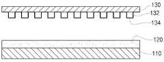
본 실시예에서는 먼저 태양전지 기판(110) 표면에 자외선 경화성 고분자 박막(120)을 형성하는 단계가 진행된다. 그리고 마이크로 패턴의 역상(132)을 가진 PDMS 몰드(130)를 제조하는 단계가 진행된다. 자외선 경화성 고분자 박막(120)을 형성하는 단계가 PDMS 몰드(130)를 제조하는 단계는 그 순서가 바뀔 수도 있고 동시에 진행될 수도 있다.In this embodiment, first, the step of forming the ultraviolet curable polymer
상기 PDMS 몰드(130)를 제조하는 단계는, a) 마이크론 패턴(132)을 형성하는 단계와 b) 이형제(134)를 코팅하는 단계로 나뉘어 진행될 수 있다. 먼저 마이크론 패턴(132)을 형성하는 단계는 기판(130) 상에 음성 감광막을 도포한 후, 사진 공정에 의하여 마이크로 패턴을 형성하는 순서로 진행될 수 있다. 그리고 이형제(134)를 코팅하는 단계는, 상기 마이크로 패턴(132) 상에 TMCS(TriMethyl Chloro Silane)와 같은 이형 성분을 기상 증착 방법에 의하여 증착하는 방법으로 진행될 수 있다. 이렇게 이형제를 코팅하면 상기 PDMS 몰드(130)를 태양전지 기판(110) 상에서 분리할 때, 이형이 용이해지는 장점이 있다.The manufacturing of the
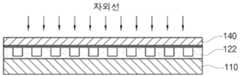
그 후에는 도 6, 7에 도시된 바와 같이 준비된 상기 PDMS 몰드(130)를 상기 자외선 경화성 고분자 박막(120)이 형성된 태양전지 기판(110) 상에 정렬한 후, 서로 접촉시켜 상기 자외선 경화성 고분자 박막(120)에 마이크론 패턴(122)을 형성시킨다. 이렇게 상기 PDMS 몰드(130)를 태양전지 기판(110)과 접촉시켜 상기 자외선 경화성 고분자 박막(120)을 변형시킨 상태에서 자외선을 조사하여 상기 태양전지 기판(110) 상에 형성된 마이크론 패턴(122)을 경화시킨다.Thereafter, the
이때 본 실시예에서는 상기 자외선 경화성 물질을 완전히 경화시키는 것이 아니라, 부분 경화시킨다. 즉, 상기 마이크론 패턴(122)이 완전히 경화된 상태가 아니라 일정하게 경화되지만, 변형될 수 있을 정도의 유연성 또는 점성은 지니고 있는 상태인 것이다. 이를 위하여 본 실시예에서는 상기 태양전지 기판(110)에 자외선을 15 ~ 25초간 조사하는 것이 바람직하다. 15초보다 짧게 조사하면 자외선 경화성 물질의 경화가 일어나지 않아서 마이크론 패턴이 아예 형성되지 않는 문제점이 있으며, 25초 이상 길게 조사하면 상기 마이크론 패턴이 완전히 경화되어 나노 패턴을 형성할 수 없는 문제점이 있다.In this embodiment, the ultraviolet curable material is partially cured, not completely cured. That is, the
다음으로는 나노 패턴을 가진 PUA 몰드(140)를 제조하는 단계가 진행된다. 상기 PUA 몰드(140)는 두께가 45 ~ 55㎛인 것이 바람직하며, 기계적 강도가 대략 40MPa 인 것이 바람직하다. 여기에서 상기 '나노 패턴'은 100nm 정도의 다양한 크기의 나노 구조물을 말하는 것이다.Next, a step of manufacturing a
이렇게 제조된 상기 PUA 몰드(140)를 도 9에 도시된 바와 같이, 부분 경화된 상기 마이크론 패턴(122) 상에 접촉하여 나노 패턴(144)를 형성시킨 후, 자외선을 조사하여 나노 패턴(144)을 경화하는 단계가 진행된다. 이렇게 하면 마이크론 패 턴(122) 상에 다수개의 나노 패턴(144)이 형성되어 초소수성이 발현되는 것이다.As shown in FIG. 9, the
도 1 내지 5는 본 발명의 일 실시예에 따른 태양전지 방진방오층 제조방법의 공정을 도시하는 공정도들이다.1 to 5 are process charts showing the process of the solar cell dustproof antifouling method according to an embodiment of the present invention.
도 6 내지 10은 본 발명의 다른 실시예에 따른 태양전지 방진방오층 제조방법의 공정을 도시하는 공정도들이다.6 to 10 are process charts showing the process of the solar cell dustproof layer manufacturing method according to another embodiment of the present invention.
Claims (8)
Translated fromKoreanPriority Applications (2)
| Application Number | Priority Date | Filing Date | Title |
|---|---|---|---|
| KR1020090049721AKR20100131045A (en) | 2009-06-05 | 2009-06-05 | Method for manufacturing dustproof antifouling layer of solar cell |
| PCT/KR2010/003601WO2010140863A2 (en) | 2009-06-05 | 2010-06-04 | Anti-dirt and anti-dust layer production method for solar cells |
Applications Claiming Priority (1)
| Application Number | Priority Date | Filing Date | Title |
|---|---|---|---|
| KR1020090049721AKR20100131045A (en) | 2009-06-05 | 2009-06-05 | Method for manufacturing dustproof antifouling layer of solar cell |
Publications (1)
| Publication Number | Publication Date |
|---|---|
| KR20100131045Atrue KR20100131045A (en) | 2010-12-15 |
Family
ID=43298341
Family Applications (1)
| Application Number | Title | Priority Date | Filing Date |
|---|---|---|---|
| KR1020090049721AWithdrawnKR20100131045A (en) | 2009-06-05 | 2009-06-05 | Method for manufacturing dustproof antifouling layer of solar cell |
Country Status (2)
| Country | Link |
|---|---|
| KR (1) | KR20100131045A (en) |
| WO (1) | WO2010140863A2 (en) |
Cited By (6)
| Publication number | Priority date | Publication date | Assignee | Title |
|---|---|---|---|---|
| KR101231258B1 (en)* | 2011-04-04 | 2013-02-07 | 엘지이노텍 주식회사 | Solar cell and manufacturing method of the same |
| KR20160089726A (en)* | 2015-01-20 | 2016-07-28 | 재단법인 멀티스케일 에너지시스템 연구단 | Polymeric film having a hybrid structured pattern and manufacturing method of same |
| WO2016200119A1 (en)* | 2015-06-08 | 2016-12-15 | 아주대학교산학협력단 | Method for forming super hydrophobic surface |
| KR20170108475A (en)* | 2016-03-18 | 2017-09-27 | 주식회사 엘지화학 | Switchable superhydrophobic film and preparing method of same |
| KR20200064370A (en)* | 2018-11-29 | 2020-06-08 | (주)휴넷플러스 | Manufacturing method of smart glass formed functional pattern |
| KR102242659B1 (en)* | 2020-09-03 | 2021-04-20 | 고려대학교 산학협력단 | Solarcell module having long-wavelength infrared ray radiating layer |
Families Citing this family (1)
| Publication number | Priority date | Publication date | Assignee | Title |
|---|---|---|---|---|
| CN105610397B (en)* | 2016-02-23 | 2018-07-03 | 上海空间电源研究所 | A kind of super thin electric curtain dust pelletizing system of energy closed loop applied to solar cell for space use battle array |
Family Cites Families (3)
| Publication number | Priority date | Publication date | Assignee | Title |
|---|---|---|---|---|
| US20070217019A1 (en)* | 2006-03-16 | 2007-09-20 | Wen-Kuei Huang | Optical components array device, microlens array and process of fabricating thereof |
| KR100855682B1 (en)* | 2007-04-16 | 2008-09-03 | 고려대학교 산학협력단 | Silicon surface texturing method of solar cell |
| KR101005300B1 (en)* | 2007-06-08 | 2011-01-04 | 고려대학교 산학협력단 | Method for manufacturing solar cell using random copolymer for optical crosslinking and thermal crosslinking |
- 2009
- 2009-06-05KRKR1020090049721Apatent/KR20100131045A/ennot_activeWithdrawn
- 2010
- 2010-06-04WOPCT/KR2010/003601patent/WO2010140863A2/enactiveApplication Filing
Cited By (6)
| Publication number | Priority date | Publication date | Assignee | Title |
|---|---|---|---|---|
| KR101231258B1 (en)* | 2011-04-04 | 2013-02-07 | 엘지이노텍 주식회사 | Solar cell and manufacturing method of the same |
| KR20160089726A (en)* | 2015-01-20 | 2016-07-28 | 재단법인 멀티스케일 에너지시스템 연구단 | Polymeric film having a hybrid structured pattern and manufacturing method of same |
| WO2016200119A1 (en)* | 2015-06-08 | 2016-12-15 | 아주대학교산학협력단 | Method for forming super hydrophobic surface |
| KR20170108475A (en)* | 2016-03-18 | 2017-09-27 | 주식회사 엘지화학 | Switchable superhydrophobic film and preparing method of same |
| KR20200064370A (en)* | 2018-11-29 | 2020-06-08 | (주)휴넷플러스 | Manufacturing method of smart glass formed functional pattern |
| KR102242659B1 (en)* | 2020-09-03 | 2021-04-20 | 고려대학교 산학협력단 | Solarcell module having long-wavelength infrared ray radiating layer |
Also Published As
| Publication number | Publication date |
|---|---|
| WO2010140863A3 (en) | 2011-03-10 |
| WO2010140863A2 (en) | 2010-12-09 |
Similar Documents
| Publication | Publication Date | Title |
|---|---|---|
| JP5597263B2 (en) | Fine structure laminate, method for producing fine structure laminate, and method for producing fine structure | |
| US10766169B2 (en) | Resin mold | |
| KR20100131045A (en) | Method for manufacturing dustproof antifouling layer of solar cell | |
| Shin et al. | Anti‐reflection and hydrophobic characteristics of M‐PDMS based moth‐eye nano‐patterns on protection glass of photovoltaic systems | |
| US20130258483A1 (en) | Glass-like polymeric antireflective films coated with silica nanoparticles, methods of making and light absorbing devices using same | |
| JP5277357B2 (en) | Inorganic composition for fine concavo-convex structure transfer | |
| US20120183690A1 (en) | Method of imprinting texture on rigid substrate using flexible stamp | |
| Lee et al. | Fabrication of highly transparent self‐cleaning protection films for photovoltaic systems | |
| CN103261812A (en) | Glass-like polymer type antireflection film, method for producing same, and light-absorbing device using same | |
| US20130199612A1 (en) | Hydrophobic substrate with anti-reflective property method for manufacturing the same, and solar cell module including the same | |
| CN103594555B (en) | A kind of preparation method with the black silicon material of self-cleaning function | |
| JP5710236B2 (en) | Microstructure laminate | |
| WO2013147105A1 (en) | Roller-shaped mold and method for producing roller-shaped mold and element | |
| TW201133901A (en) | Guard substrate for optical electromotive force equipment, and its production process | |
| JP5956198B2 (en) | Lens for concentrating solar cell and method for manufacturing lens for concentrating solar cell | |
| Amalathas et al. | Upright nanopyramid structured cover glass with light harvesting and self-cleaning effects for solar cell applications | |
| Leem et al. | Hierarchical structured polymers for light-absorption enhancement of silicon-based solar power systems | |
| KR101123821B1 (en) | Method for treating a surface of solar cell and solar cell manufactured by the same | |
| US20240053677A1 (en) | Apparatus and Method for Structured Replication and Transfer | |
| JP2012101483A (en) | Resin mold manufacturing method | |
| JP2015115436A (en) | Functional transfer body and functional layer transfer method | |
| Choi et al. | Analysis of optical and wetting properties of a biomimetic anti-reflective surface for practical application | |
| JP6324048B2 (en) | Functional transfer body, method of transferring functional layer, solar cell and method of manufacturing the same | |
| JP6132545B2 (en) | Laminate for fine pattern formation | |
| TW201517294A (en) | Method for manufacturing nanostructure of solar cell |
Legal Events
| Date | Code | Title | Description |
|---|---|---|---|
| PA0109 | Patent application | Patent event code:PA01091R01D Comment text:Patent Application Patent event date:20090605 | |
| PG1501 | Laying open of application | ||
| PC1203 | Withdrawal of no request for examination | ||
| WITN | Application deemed withdrawn, e.g. because no request for examination was filed or no examination fee was paid |