KR20100129075A - Nonvolatile Memory Device and Its Program Method - Google Patents
Nonvolatile Memory Device and Its Program MethodDownload PDFInfo
- Publication number
- KR20100129075A KR20100129075AKR1020090047832AKR20090047832AKR20100129075AKR 20100129075 AKR20100129075 AKR 20100129075AKR 1020090047832 AKR1020090047832 AKR 1020090047832AKR 20090047832 AKR20090047832 AKR 20090047832AKR 20100129075 AKR20100129075 AKR 20100129075A
- Authority
- KR
- South Korea
- Prior art keywords
- bit line
- program
- sensing node
- potential
- discharging
- Prior art date
- Legal status (The legal status is an assumption and is not a legal conclusion. Google has not performed a legal analysis and makes no representation as to the accuracy of the status listed.)
- Withdrawn
Links
- 238000007599dischargingMethods0.000claimsabstractdescription20
- 238000000034methodMethods0.000claimsdescription14
- 230000004044responseEffects0.000claimsdescription14
- 238000010586diagramMethods0.000description6
- 230000001351cycling effectEffects0.000description3
- 230000014759maintenance of locationEffects0.000description3
- 230000005684electric fieldEffects0.000description2
- 239000011159matrix materialSubstances0.000description2
- 230000007704transitionEffects0.000description2
- 230000003213activating effectEffects0.000description1
- 238000007796conventional methodMethods0.000description1
- 238000013500data storageMethods0.000description1
- 230000006870functionEffects0.000description1
- 230000010354integrationEffects0.000description1
- 230000008672reprogrammingEffects0.000description1
Images

Classifications
- G—PHYSICS
- G11—INFORMATION STORAGE
- G11C—STATIC STORES
- G11C16/00—Erasable programmable read-only memories
- G11C16/02—Erasable programmable read-only memories electrically programmable
- G11C16/06—Auxiliary circuits, e.g. for writing into memory
- G11C16/10—Programming or data input circuits
- G—PHYSICS
- G11—INFORMATION STORAGE
- G11C—STATIC STORES
- G11C16/00—Erasable programmable read-only memories
- G11C16/02—Erasable programmable read-only memories electrically programmable
- G11C16/06—Auxiliary circuits, e.g. for writing into memory
- G11C16/24—Bit-line control circuits
- G—PHYSICS
- G11—INFORMATION STORAGE
- G11C—STATIC STORES
- G11C16/00—Erasable programmable read-only memories
- G11C16/02—Erasable programmable read-only memories electrically programmable
- G11C16/06—Auxiliary circuits, e.g. for writing into memory
- G11C16/34—Determination of programming status, e.g. threshold voltage, overprogramming or underprogramming, retention
- G11C16/3436—Arrangements for verifying correct programming or erasure
- G11C16/3454—Arrangements for verifying correct programming or for detecting overprogrammed cells
- G11C16/3459—Circuits or methods to verify correct programming of nonvolatile memory cells
- G—PHYSICS
- G11—INFORMATION STORAGE
- G11C—STATIC STORES
- G11C11/00—Digital stores characterised by the use of particular electric or magnetic storage elements; Storage elements therefor
- G11C11/56—Digital stores characterised by the use of particular electric or magnetic storage elements; Storage elements therefor using storage elements with more than two stable states represented by steps, e.g. of voltage, current, phase, frequency
- G11C11/5621—Digital stores characterised by the use of particular electric or magnetic storage elements; Storage elements therefor using storage elements with more than two stable states represented by steps, e.g. of voltage, current, phase, frequency using charge storage in a floating gate
- G11C11/5628—Programming or writing circuits; Data input circuits
- G—PHYSICS
- G11—INFORMATION STORAGE
- G11C—STATIC STORES
- G11C2211/00—Indexing scheme relating to digital stores characterized by the use of particular electric or magnetic storage elements; Storage elements therefor
- G11C2211/56—Indexing scheme relating to G11C11/56 and sub-groups for features not covered by these groups
- G11C2211/564—Miscellaneous aspects
- G11C2211/5642—Multilevel memory with buffers, latches, registers at input or output
Landscapes
- Read Only Memory (AREA)
Abstract
Translated fromKoreanDescription
Translated fromKorean본 발명은 불휘발성 메모리 장치 및 이의 프로그램 방법에 관한 것으로 프로그램 동작시 고전압으로 인한 셀 스트레스를 완화시킬 수 있는 불휘발성 메모리 장치 및 이의 프로그램 방법에 관한 것이다.The present invention relates to a nonvolatile memory device and a program method thereof, and to a nonvolatile memory device and a program method thereof that can alleviate cell stress due to high voltage during a program operation.
최근 불휘발성 메모리 장치는 고집적화, 고용량화를 위해 싱글 레벨 셀(Single Level Cell, SLC)에서 멀티 레벨 셀(Multi Level Cell, MLC)로 전환되고 있다. 싱글 레벨 셀은 '1' 또는 '0'의 논리 값을 가지는 1-비트의 데이터가 저장될 수 있고, 멀티 레벨 셀은 '11', '10', '01', '00' 중 어느 하나의 논리 값을 가지는 2-비트의 데이터가 저장될 수 있다. 따라서, 멀티 레벨 셀들을 포함하는 불휘발성 메모리 장치는 대용량의 데이터 저장 공간을 필요로 하는 고집적화된 장치로서 사용된다.Recently, nonvolatile memory devices have been switched from single level cells (SLCs) to multi level cells (MLCs) for high integration and high capacity. The single level cell may store 1-bit data having a logic value of '1' or '0', and the multi level cell may store any one of '11', '10', '01' and '00'. 2-bit data having a logical value may be stored. Accordingly, nonvolatile memory devices including multi-level cells are used as highly integrated devices that require large amounts of data storage space.
불휘발성 메모리 장치는 통상적으로 데이터가 저장되는 셀들이 매트릭스 형 태로 구성된 메모리 셀 어레이, 상기 메모리 셀 어레이의 특정 셀들에 대하여 메모리를 기입하거나 특정 셀에 저장되었던 메모리를 독출하는 페이지 버퍼를 포함한다. 상기 페이지 버퍼는 특정 메모리 셀과 접속된 비트라인 쌍, 메모리 셀 어레이에 기록할 데이터를 임시저장하거나, 메모리 셀 어레이로부터 특정 셀의 데이터를 독출하여 임시 저장하는 레지스터, 특정 비트라인 또는 특정 레지스터의 전압 레벨을 감지하는 감지노드, 상기 특정 비트라인과 감지노드의 접속여부를 제어하는 비트라인 선택부를 포함한다.A nonvolatile memory device typically includes a memory cell array in which cells in which data is stored is configured in a matrix form, and a page buffer for writing a memory to a specific cell of the memory cell array or reading a memory stored in the specific cell. The page buffer may include a pair of bit lines connected to a specific memory cell, a register for temporarily storing data to be written to the memory cell array, or a register for reading and temporarily storing data of a specific cell from the memory cell array, a voltage of a specific bit line or a specific register. It includes a sensing node for sensing a level, a bit line selection unit for controlling the connection of the specific bit line and the sensing node.
이러한 불휘발성 메모리 장치의 각 메모리 셀은 전기적인 프로그램 및 소거동작이 가능한 소자로서, 약 100Å의 얇은 산화막(이하, 터널 산화막)에 강한 전기장에 의해 전자가 이동하면서 셀의 문턱전압을 변화시켜 프로그램 및 소거 기능을 수행한다.Each memory cell of such a nonvolatile memory device is an electric program and an erasable device. The electrons are moved by a strong electric field in a thin oxide film (hereinafter, referred to as a tunnel oxide film) of about 100 Å to change the threshold voltage of the cell. Perform the erase function.
일반적으로 불휘발성 메모리 장치의 프로그램 동작은 ISPP(Incremental Step Pulse Programming) 방식을 사용하여 특정 전압 레벨에서 검증(verify) 전압 레벨을 넘어가지 못한 셀에 대해 일정한 스텝 전압을 올려 다시 프로그램하는 방식이다.In general, a program operation of a nonvolatile memory device is a method of raising and reprogramming a constant step voltage for a cell that has not exceeded a verify voltage level at a specific voltage level using an incremental step pulse programming (ISPP) method.
그리고 프로그램을 위해 선택되는 메모리 셀이 연결되는 비트라인에는 0V를 인가하고, 다른 비트라인에는 전원전압(Vcc)을 인가하여 프로그램이 되는 것을 방지한다.In addition, 0V is applied to the bit line to which the memory cell selected for the program is connected, and a power supply voltage Vcc is applied to the other bit line to prevent programming.
상기한 프로그램 방법은 셀의 문턱전압 분포를 확보하기 위해 프로그램 전압을 시작전압으로부터 일정한 전압 스텝으로 증가시키면서 특정 검증 전압을 넘길 때까지 프로그램을 진행한다.In order to secure the threshold voltage distribution of the cell, the program method increases the program voltage from the start voltage to a constant voltage step and proceeds the program until a specific verify voltage is exceeded.
종래 기술에 따른 불휘발성 메모리 소자의 프로그램 방법은 선택된 메모리 셀의 게이트에 14V 내지 20V의 고전압이 인가되어 셀이 받는 스트레스가 갑자기 증가하게 된다. 이로 인하여 메모리 셀의 리텐션 특성 및 사이클링 특성등이 저하되는 문제점이 야기된다.In the conventional method of programming a nonvolatile memory device, a high voltage of 14 V to 20 V is applied to a gate of a selected memory cell, thereby suddenly increasing stress of the cell. This causes a problem that the retention characteristics and cycling characteristics of the memory cell are degraded.
본 발명이 이루고자 하는 기술적 과제는 ISPP 방식을 이용한 불휘발성 메모리 장치의 프로그램 동작에 있어서, 첫번째 프로그램 바이어스가 인가되는 동안 프로그램하려는 비트라인의 전위를 디스차지함으로써, 메모리 셀이 받는 스트레스를 완화시켜 불휘발성 메모리 장치의 리텐션 특성 및 사이클링 특성을 개선시킬 수 있는 불휘발성 메모리 장치 및 이의 프로그램 방법을 제공하는 데 있다.The technical problem to be achieved by the present invention is to program the nonvolatile memory device using the ISPP method, by discharging the potential of the bit line to be programmed while the first program bias is applied, thereby reducing the stress of the memory cell to reduce the nonvolatile The present invention provides a nonvolatile memory device and a program method thereof capable of improving retention characteristics and cycling characteristics of a memory device.
본 발명의 제1 시 예에 따른 불휘발성 메모리 장치는 다수의 메모리 셀들이 비트라인에 연결된 메모리 셀 어레이, 및 상기 비트라인과 입출력 단자 사이에 연결되며, ISPP 프로그램 동작시 상기 비트라인을 프리차지한 후, 첫 번째 프로그램 전압이 상기 다수의 메모리 셀등 중 선택된 메모리 셀에 인가되는 동안 상기 비트라인을 디스차지하는 페이지 버퍼를 포함한다.In a nonvolatile memory device according to a first embodiment of the present invention, a memory cell array having a plurality of memory cells connected to a bit line, and connected between the bit line and an input / output terminal, after precharging the bit line during an ISPP program operation, And a page buffer for discharging the bit line while a first program voltage is applied to a selected one of the plurality of memory cells.
상기 페이지 버퍼는 상기 비트라인을 감지 노드에 연결하는 비트라인 선택부와, 상기 감지 노드를 프리차지하는 프리차지부, 및 프로그램 데이터 값에 따라 상기 감지 노드 및 상기 비트라인의 전위를 디스차지하는 래치부를 포함한다.The page buffer includes a bit line selector for connecting the bit line to a sense node, a precharge unit for precharging the sense node, and a latch unit for discharging potentials of the sense node and the bit line according to a program data value. do.
상기 래치부는 상기 첫번째 프로그램 전압이 인가되는 동안 상기 감지 노드와 연결된 상기 비트라인의 전위를 디스차지한다.The latch unit discharges the potential of the bit line connected to the sensing node while the first program voltage is applied.
본 발명의 제2 실시 예에 따른 불휘발성 메모리 장치는 다수의 메모리 셀들이 비트라인에 연결된 메모리 셀 어레이, 및 상기 비트라인과 입출력 단자 사이에 연결되며, ISPP 프로그램 동작시 상기 비트라인을 프리차지한 후, 첫 번째 프로그램 전압이 상기 다수의 메모리 셀등 중 선택된 메모리 셀에 인가되는 동안 상기 비트라인을 디스차지하는 페이지 버퍼를 포함하며, 상기 페이지 버퍼는 상기 비트라인의 전위를 디스차지하는 디스차지부를 포함한다.In a nonvolatile memory device according to a second embodiment of the present invention, a memory cell array having a plurality of memory cells connected to a bit line, and connected between the bit line and an input / output terminal, after precharging the bit line during an ISPP program operation, And a page buffer for discharging the bit line while a first program voltage is applied to a selected memory cell among the plurality of memory cells. The page buffer includes a discharge unit for discharging a potential of the bit line.
상기 페이지 버퍼는 상기 비트라인을 감지 노드에 연결하는 비트라인 선택부와, 상기 감지 노드를 프리차지하는 프리차지부와, 프로그램 데이터 값을 임시 저장하고, 상기 첫번째 프로그램 전압이 인가된 이후에 인가되는 다음 프로그램이 인가될 때 상기 프로그램 데이터 값에 따라 상기 감지 노드 및 상기 비트라인의 전위를 디스차지하는 래치부, 및 상기 비트라인에 연결되고, 제어 신호에 응답하여 상기 비트라인의 전위를 디스차지하는 상기 디스차지부를 포함한다.The page buffer temporarily stores a bit line selector for connecting the bit line to the sense node, a precharge unit for precharging the sense node, a program data value, and is applied after the first program voltage is applied. A latch unit for discharging the potential of the sensing node and the bit line when the program is applied, and the discharge unit connected to the bit line and discharging the potential of the bit line in response to a control signal Contains wealth.
상기 디스차지부는 상기 비트라인과 접지 전원 사이에 직렬 연결된 다수의 트랜지스터들을 포함하며, 상기 디스차지부는 상기 제어신호에 응답하여 디스차지되는 시간을 제어한다.The discharge unit includes a plurality of transistors connected in series between the bit line and the ground power source, and the discharge unit controls the discharge time in response to the control signal.
본 발명의 일실시 예에 따른 불휘발성 메모리 장치의 프로그램 방법은 불휘발성 메모리 소자의 ISPP 프로그램 방법에 있어서, 메모리 셀이 연결된 비트라인을 프리차지하는 단계와, 상기 메모리 셀의 워드라인에 제1 프로그램 전압을 인가하는 단계와, 상기 제1 프로그램 전압이 인가되는 동안 상기 비트라인의 전위를 디스차 지하는 단계와, 상기 제1 프로그램 전압이 인가되는 구간 후, 상기 비트라인을 재프리차지하는 단계와, 상기 비트라인을 디스차지하는 단계, 및 상기 메모리 셀의 워드라인에 제2 프로그램 전압을 인가하는 단계를 포함한다.A method of programming a nonvolatile memory device according to an exemplary embodiment of the present invention includes the steps of: precharging a bit line to which a memory cell is connected in a ISPP program method of a nonvolatile memory device, and a first program voltage on a word line of the memory cell. Applying a voltage, discharging the potential of the bit line while the first program voltage is applied, re-charging the bit line after a period in which the first program voltage is applied, and Discharging a bit line, and applying a second program voltage to a word line of the memory cell.
본 발명의 실시 예에 따르면, ISPP 방식을 이용한 불휘발성 메모리 장치의 프로그램 동작에 있어서, 첫번째 프로그램 바이어스가 인가되는 동안 프로그램하려는 비트라인의 전위를 디스차지함으로써, 메모리 셀이 받는 스트레스를 완화시켜 불휘발성 메모리 장치의 리텐션 특성 및 사이클링 특성을 개선시킬 수 있다.According to an embodiment of the present invention, in a program operation of a nonvolatile memory device using the ISPP method, by discharging the potential of a bit line to be programmed while the first program bias is applied, the stress of the memory cell is reduced to reduce the nonvolatile The retention characteristics and the cycling characteristics of the memory device can be improved.
이하, 첨부된 도면을 참조하여 본 발명의 바람직한 실시 예를 설명하기로 한다. 그러나 본 발명은 이하에서 개시되는 실시 예에 한정되는 것이 아니라 서로 다른 다양한 형태로 구현될 수 있으며, 단지 본 실시 예는 본 발명의 개시가 완전하도록 통상의 지식을 가진자에게 발명의 범주를 완전하게 알려주기 위해 제공되는 것이다.Hereinafter, preferred embodiments of the present invention will be described with reference to the accompanying drawings. As those skilled in the art would realize, the described embodiments may be modified in various different ways, all without departing from the spirit or scope of the present invention. It is provided to inform you.
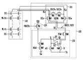
도 1은 본 발명의 제1 실시 예에 따른 불휘발성 메모리 장치를 나타내는 회로도이다.1 is a circuit diagram illustrating a nonvolatile memory device according to a first embodiment of the present invention.
도 1을 참조하면, 불휘발성 메모리 장치는 메모리 셀 어레이(100), 및 페이 지 버퍼(200)를 포함한다.Referring to FIG. 1, a nonvolatile memory device includes a
메모리 셀 어레이(100)는 데이타를 저장하는 메모리 셀들과, 메모리 셀들을 선택하여 활성화하는 워드 라인들과, 메모리 셀의 데이타를 입출력할 수 있는 비트 라인들(BLe, BLo)을 포함하며, 복수개의 워드 라인들 및 복수개의 비트 라인들이 메트릭스 형태로 배열된 구조이다. 메모리 셀 어레이(100)는 소스 선택 트랜지스터와 드레인 선택 트랜지스터들 사이에 직렬 연결된 메모리 셀들을 포함하는데 이를 스트링(string) 구조라 한다. 메모리 셀들의 게이트는 워드 라인들에 연결되며, 동일한 워드 라인에 공통으로 연결된 메모리 셀들의 집합을 페이지(page)라 한다. 각각의 비트 라인에 연결된 복수개의 스트링들이 공통 소스 라인에 병렬로 연결되어 블록(block)을 구성한다.The
페이저 버퍼(200)는 비트라인 선택부(210), 프리차지부(220), 및 래치부(230)를 포함한다.The
비트라인 선택부(210)는 다수의 NMOS 트랜지스터(NM1 내지 NM4)를 포함한다. NMOS 트랜지스터(NM1)는 제1 디스차지 신호(DISCHe)에 응답하여 제어 전압(VIRPWR)을 이븐 비트라인(BLe)에 인가한다. NMOS 트랜지스터(NM2)는 제2 디스차지 신호(DISCHo)에 응답하여 제어 전압(VIRPWR)을 오드 비트라인(BLo)에 인가한다.The
NMOS 트랜지스터(NM3)는 이븐 비트라인(BLe)과 감지 노드(SO) 사이에 연결되고, 제1 비트라인 선택신호(BSLe)에 응답하여 이븐 비트라인(BLe)과 감지 노드(SO)를 연결한다. NMOS 트랜지스터(NM4)는 오드 비트라인(BLo)과 감지 노드(SO) 사이에 연결되고, 제2 비트라인 선택신호(BSLo)에 응답하여 오드 비트라인(BLo)과 감지 노 드(SO)를 연결한다.The NMOS transistor NM3 is connected between the even bit line BLe and the sensing node SO, and connects the even bit line BLe and the sensing node SO in response to the first bit line selection signal BSLe. . The NMOS transistor NM4 is connected between the odd bit line BLo and the sensing node SO, and connects the odd bit line BLo and the sensing node SO in response to the second bit line selection signal BSLo. do.
프리차지부(220)는 PMOS 트랜지스터(PM1)를 포함한다. PMOS 트랜지스터(PM1)는 감지 노드(SO)와 전원 전압(VDD) 사이에 연결되고, 프리차지신호(PRECHb)에 응답하여 감지 노드(SO)에 전원 전압(VDD)을 인가한다. The
래치부(230)는 다수의 NMOS 트랜지스터(NM5 내지 NM9) 및 인버터(IV1 및 IV2)를 포함한다.The
인버터(IV1 및 IV2)는 제1 노드(Q)와 제2 노드(Qb) 사이에 역방향 병렬 연결되어 데이터를 임시 저장할 수 있는 래치(LATCH) 구조로 배치된다. NMOS 트랜지스터(NM5)는 감지 노드(SO)와 제2 노드(Qb) 사이에 연결되고, 프로그램 신호(PGM)에 응답하여 감지 노드(SO)와 제2 노드(Qb)를 연결한다. NMOS 트랜지스터(NM6) 및 NMOS 트랜지스터(NM7)는 제1 노드(Q)와 접지 전원(Vss) 사이에 직렬 연결된다. NMOS 트랜지스터(NM6)는 감지 노드(SO)의 전위에 따라 제어되고, NMOS 트랜지스터(NM7)는 독출 신호(READ)에 응답하여 제어된다. NMOS 트랜지스터(NM8) 및 NMOS 트랜지스터(NM9)는 제1 노드(Q) 및 제2 노드(Qb)와 입출력 단자(YA) 사이에 각각 연결되고, 제1 및 제2 데이터 입력 신호(nDI, 및 DI)에 응답하여 입출력 단자(YA)를 제1 노드(Q) 또는 제2 노드(Qb)에 연결한다.Inverters IV1 and IV2 are arranged in a latch structure to temporarily store data by being connected in reverse parallel between the first node Q and the second node Qb. The NMOS transistor NM5 is connected between the sensing node SO and the second node Qb and connects the sensing node SO and the second node Qb in response to the program signal PGM. The NMOS transistor NM6 and the NMOS transistor NM7 are connected in series between the first node Q and the ground power supply Vss. The NMOS transistor NM6 is controlled according to the potential of the sensing node SO, and the NMOS transistor NM7 is controlled in response to the read signal READ. The NMOS transistor NM8 and the NMOS transistor NM9 are connected between the first node Q and the second node Qb and the input / output terminal YA, respectively, and the first and second data input signals nDI and DI. ) Connects the input / output terminal YA to the first node Q or the second node Qb.
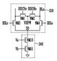
도 2는 도 1에 도시된 본원 발명의 페이지 버퍼(200)에 추가적으로 배치될 수 있는 디스차지부(240)를 나타내는 회로도이다.FIG. 2 is a circuit diagram illustrating a
도 2를 참조하면, 디스차지부(240)는 도 1의 페이지 버퍼(200)의 감지 노 드(SO)에 연결된다. 디스차지부(240)는 다수의 NMOS 트랜지스터(NM10 및 NM11)를 포함한다. NMOS 트랜지스터(NM10 및 NM11)는 감지 노드(SO)와 접지 전원(Vss) 사이에 직렬 연결되며, 제1 및 제2 제어 신호(Va 및 Vb)에 응답하여 감지 노드(SO)를 접지 전원(Vss)과 연결시킨다.Referring to FIG. 2, the
도 3은 본 발명의 불휘발성 메모리 소자의 프로그램 동작을 설명하기 위한 프로그램 전압 및 비트라인(BLe 및 BLo) 전위를 나타내는 파형도이다.3 is a waveform diagram illustrating a program voltage and potentials of bit lines BLe and BLo for explaining a program operation of the nonvolatile memory device of the present invention.
도 1 및 도 3을 참조하여 본 발명의 제1 실시 예에 따른 불휘발성 메모리 소자의 프로그램 동작을 설명하면 다음과 같다.A program operation of the nonvolatile memory device according to the first embodiment of the present invention will be described with reference to FIGS. 1 and 3 as follows.
본 발명의 실시 예는 이븐 비트라인(BLe)에 연결된 메모리 셀의 프로그램 동작을 일예로 설명하며, 프로그램 방법은 순차적으로 스텝 전위만큼 상승된 프로그램 전압을 사용하는 ISPP 방식을 이용한다.An embodiment of the present invention describes a program operation of a memory cell connected to an even bit line Ble as an example, and the program method uses an ISPP method that uses a program voltage sequentially increased by a step potential.
페이지 버퍼(200)의 래치부(230)에 하이 레벨의 제2 데이터 입력 신호(DI)가 입력되어 NMOS 트랜지스터(NM9)가 턴온된다. 이로 인하여 제2 노드(Qb)와 입출력 단자(YA)가 연결된다. 프로그램 동작시 입출력 단자(YA)는 접지 전원(Vss)과 연결되어 있어, 제2 노드(Qb)는 로우 레벨이 된다.The second data input signal DI having a high level is input to the
로우 레벨의 프리차지 신호(PRECHb)가 일정 시간 동안 인가되어 감지 노드(SO)를 하이 레벨로 프리차지한다. 또한 로우 레벨의 제1 디스차지 신호(DSICHe)에 응답하여 NMOS 트랜지스터(NM1)가 턴오프되어 이븐 비트라인(BLe)에 인가되던 제어 전압(VIRPWR)이 차단된다. 또한, 하이 레벨의 제1 비트라인 선택신호(BSLe)에 응답하여 턴온되어 비트라인(BLe)과 감지 노드(SO)를 연결한다. 이로 인하여 이븐 비트라인(BLe)은 하이 레벨로 프리차지된다.The low level precharge signal PRECHb is applied for a predetermined time to precharge the sensing node SO to a high level. In addition, the NMOS transistor NM1 is turned off in response to the low-level first discharge signal DSICHe to block the control voltage VIRPWR applied to the even bit line BLe. The bit line BLe and the sensing node SO are turned on in response to the high level first bit line selection signal BSLe. As a result, the even bit line BLe is precharged to a high level.
일정 시간 후, 프리차지 신호(PRECHb)가 하이 레벨로 천이되어 전원 전압(VDD)을 차단하고, 제1 비트라인 선택신호(BSLe)가 로우 레벨로 천이하여 이븐 비트라인(BLe)과 감지 노드(SO)의 연결을 차단한다.After a predetermined time, the precharge signal PRECHb transitions to a high level to block the power supply voltage VDD, and the first bit line selection signal BSLe transitions to a low level so that the even bit line BLe and the sensing node ( Disconnect the SO.
이 후, 다수의 워드라인(WL<0> 내지 WL<31>) 중 선택된 워드라인(예를 들어 WL<0>)에 ISPP 방식의 제1 프로그램 전압(Vpgm)이 인가된다.Thereafter, the first program voltage Vpgm of the ISPP method is applied to the selected word lines (eg, WL <0>) among the plurality of word lines WL <0> to WL <31>.
선택된 워드라인(WL<0>)에 제1 프로그램 전압(Vpgm)이 인가되는 동안 페이지 버퍼(200)에 제1 비트라인 선택신호(BSLe) 및 프로그램 신호(PGM)가 인가된다. 이로 인하여 하이 레벨로 프리차지되어 있는 이븐 비트라인(BLe) 및 감지 노드(SO)는 제2 노드(Qb)에 의해 로우 레벨로 디스차지된다.(DISCH_PATH) 이때 제1 비트라인 선택신호(BSLe) 및 프로그램 신호(PGM)의 로직 레벨을 제어하여 디스차지되는 시간을 조절할 수 있다. 일반적으로 제1 비트라인 선택신호(BSLe) 및 프로그램 신호(PGM)의 로직 레벨은 전압 발생기의 출력 전위를 변경하여 제어할 수 있다.The first bit line selection signal BSLe and the program signal PGM are applied to the
이로 인하여 프로그램 동작시 메모리 셀에 제1 프로그램 전압(Vpgm)이 인가되는 동안 초기 이븐 비트라인(BLe)을 하이 레벨로 프리차지된 상태에서 점차 디스차지함으로써 메모리 셀에 인가되는 셀스트레스를 감소시킬 수 있다.Accordingly, the cell stress applied to the memory cell may be reduced by gradually discharging the initial even bit line BLe while precharging the first even voltage line Vpgm to the memory cell during the program operation. have.
제1 프로그램 전압(Vpgm1)이 인가되는 프로그램 동작이 완료되면 상술한 방법과 동일하게 이븐 비트라인(BLe)을 프리차지한다. 이 후, 제1 프로그램 전압(Vpgm1)보다 스텝 전압(Vstep)만큼 상승된 제2 프로그램 전압(Vpgm2)이 인가되기 이전에 이븐 비트라인(BLe)을 로우 레벨로 디스차지한다. 이는 메모리 셀이 가장 많은 전계 변화를 받는 제1 프로그램 전압(Vpgm1)이 인가되는 구간에서만 이븐 비트라인(BLe)을 천천히 디스차지하고, 다음 프로그램 구간(Vpgm2, Vpgm3)에서는 프로그램 전압이 인가되기 이전에 이븐 비트라인(BLe)을 디스차지한다.When the program operation to which the first program voltage Vpgm1 is applied is completed, the even bit line BLe is precharged in the same manner as described above. Thereafter, the even bit line BLe is discharged to a low level before the second program voltage Vpgm2 that is increased by the step voltage Vstep is applied to the first program voltage Vpgm1. It slowly discharges the even bit line BLe only in a section where the first program voltage Vpgm1 receiving the most electric field change is applied to the memory cell, and even before the program voltage is applied in the next program sections Vpgm2 and Vpgm3. The bit line BLe is discharged.
상술한 ISPP 방식의 프로그램 동작은 각각의 프로그램 전압(Vpgm1, Vpgm2, Vpgm3)이 인가되는 구간이 종료되면 프로그램 검증 동작을 실시하여 프로그램 동작을 종료할 것인지 다음 프로그램 전압을 인가할 것인지 제어할 수 있다.The program operation of the ISPP method described above may control whether to terminate the program operation or to apply the next program voltage by performing a program verification operation when the sections to which the respective program voltages Vpgm1, Vpgm2, and Vpgm3 are applied.
도 2에 따른 디스차지부(240)를 포함하는 페이지 버퍼(200)를 이용한 프로그램 동작시를 설명하면 다음과 같다.A program operation using the
먼저 상술한 방법과 같이 이븐 비트라인(BLe)을 하이 레벨로 프리차지한다. 이 후, 제1 프로그램 전압(Vpgm)이 인가되는 동안 페이지 버퍼(200)의 디스차지부(240)에 제1 및 제2 제어 신호(Va 및 Vb)가 인가되어 이븐 비트라인(BLe)을 로우 레벨로 디스차지한다. 이때 인가되는 제1 및 제2 제어 신호(Va 및 Vb)의 전위를 제어하여 이븐 비트라인(BLe)을 디스차지하는 시간을 제어할 수 있다.First, the even bit line BLe is precharged to a high level as described above. Thereafter, the first and second control signals Va and Vb are applied to the
디스차지부(240)를 이용하여 이븐 비트라인(BLe)을 디스차지하는 동작은 ISPP 방식의 제1 프로그램 전압(Vpgm1)이 인가되는 구간에서만 사용되며, 제2 프로그램 전압(Vpgm2) 및 제3 프로그램 전압(Vpgm3)이 인가되는 구간에서는 래치부(230)를 이용하여 이븐 비트라인(BLe)의 전위를 제어하는 것이 바람직하다.The operation of discharging the even bit line BLe using the
상기에서 설명한 본 발명의 기술적 사상은 바람직한 실시 예에서 구체적으로 기술되었으나, 상기한 실시 예는 그 설명을 위한 것이며 그 제한을 위한 것이 아님을 주의하여야 한다. 또한, 본 발명은 본 발명의 기술 분야의 통상의 전문가라면 본 발명의 기술적 사상의 범위 내에서 다양한 실시예가 가능함을 이해할 수 있을 것이다.Although the technical spirit of the present invention described above has been described in detail in a preferred embodiment, it should be noted that the above-described embodiment is for the purpose of description and not of limitation. In addition, the present invention will be understood by those skilled in the art that various embodiments are possible within the scope of the technical idea of the present invention.
도 1은 본 발명의 제1 실시 예에 따른 불휘발성 메모리 장치를 나타내는 회로도이다.1 is a circuit diagram illustrating a nonvolatile memory device according to a first embodiment of the present invention.
도 2는 도 1에 도시된 본원 발명의 페이지 버퍼(200)에 추가적으로 배치될 수 있는 디스차지부(240)를 나타내는 회로도이다.FIG. 2 is a circuit diagram illustrating a
도 3은 본 발명의 불휘발성 메모리 소자의 프로그램 동작을 설명하기 위한 프로그램 전압 및 비트라인(BLe 및 BLo) 전위를 나타내는 파형도이다.3 is a waveform diagram illustrating a program voltage and potentials of bit lines BLe and BLo for explaining a program operation of the nonvolatile memory device of the present invention.
<도면의 주요 부분에 대한 부호 설명><Description of the symbols for the main parts of the drawings>
100 : 메모리 셀 어레이200 : 페이지 버퍼100: memory cell array 200: page buffer
210 : 비트라인 선택부220 : 프리차지부210: bit line selection unit 220: precharge unit
230 : 래치부240 : 디스차지부230: latch portion 240: discharge portion
Claims (8)
Translated fromKoreanPriority Applications (1)
| Application Number | Priority Date | Filing Date | Title |
|---|---|---|---|
| KR1020090047832AKR20100129075A (en) | 2009-05-29 | 2009-05-29 | Nonvolatile Memory Device and Its Program Method |
Applications Claiming Priority (1)
| Application Number | Priority Date | Filing Date | Title |
|---|---|---|---|
| KR1020090047832AKR20100129075A (en) | 2009-05-29 | 2009-05-29 | Nonvolatile Memory Device and Its Program Method |
Publications (1)
| Publication Number | Publication Date |
|---|---|
| KR20100129075Atrue KR20100129075A (en) | 2010-12-08 |
Family
ID=43505859
Family Applications (1)
| Application Number | Title | Priority Date | Filing Date |
|---|---|---|---|
| KR1020090047832AWithdrawnKR20100129075A (en) | 2009-05-29 | 2009-05-29 | Nonvolatile Memory Device and Its Program Method |
Country Status (1)
| Country | Link |
|---|---|
| KR (1) | KR20100129075A (en) |
Cited By (1)
| Publication number | Priority date | Publication date | Assignee | Title |
|---|---|---|---|---|
| US10109362B2 (en) | 2016-10-17 | 2018-10-23 | SK Hynix Inc. | Semiconductor device and method for operating the same |
- 2009
- 2009-05-29KRKR1020090047832Apatent/KR20100129075A/ennot_activeWithdrawn
Cited By (1)
| Publication number | Priority date | Publication date | Assignee | Title |
|---|---|---|---|---|
| US10109362B2 (en) | 2016-10-17 | 2018-10-23 | SK Hynix Inc. | Semiconductor device and method for operating the same |
Similar Documents
| Publication | Publication Date | Title |
|---|---|---|
| JP4744819B2 (en) | FLASH MEMORY DEVICE HAVING MULTI-LEVEL CELL AND ITS READING METHOD AND PROGRAM METHOD | |
| US7417899B2 (en) | Method of verifying flash memory device | |
| KR0169267B1 (en) | Nonvolatile Semiconductor Memory | |
| JP4510060B2 (en) | Read / write control method for nonvolatile semiconductor memory device | |
| US7558117B2 (en) | Nonvolatile semiconductor memory device | |
| US7561474B2 (en) | Program verifying method and programming method of flash memory device | |
| US20080144370A1 (en) | Method of programming multi-level cells and non-volatile memory device including the same | |
| US8023330B2 (en) | Method of erasing a nonvolatile memory device | |
| KR101005117B1 (en) | How Nonvolatile Memory Devices Work | |
| US8085587B2 (en) | Non-volatile memory device and method of verifying a program operation in the same | |
| KR100960448B1 (en) | Program Verification Method of Nonvolatile Memory Device | |
| WO2009081745A1 (en) | Nonvolatile semiconductor storage device | |
| KR20090036839A (en) | How to Program Nonvolatile Memory Devices | |
| US8279675B2 (en) | Nonvolatile memory device and method of programming the same | |
| JP2009043390A (en) | Soft program method in non-volatile memory device | |
| US8351270B2 (en) | Nonvolatile memory device and method of programming the device | |
| CN101071640B (en) | Methods of Verifying Flash Memory Devices | |
| US7403431B2 (en) | Method of reading a flash memory device | |
| JP5242603B2 (en) | Semiconductor memory device | |
| US7782676B2 (en) | Method of operating a nonvolatile memory device | |
| KR20080102037A (en) | Verification method and post program method of multi-level cell NAND flash memory devices | |
| KR20100129075A (en) | Nonvolatile Memory Device and Its Program Method | |
| KR100861648B1 (en) | Soft Program Method for Nonvolatile Memory Devices | |
| KR20090000332A (en) | Data reading method of nonvolatile memory device | |
| KR100881520B1 (en) | Data reading method and program verification method of nonvolatile memory device and nonvolatile memory device |
Legal Events
| Date | Code | Title | Description |
|---|---|---|---|
| PA0109 | Patent application | Patent event code:PA01091R01D Comment text:Patent Application Patent event date:20090529 | |
| PG1501 | Laying open of application | ||
| PC1203 | Withdrawal of no request for examination | ||
| WITN | Application deemed withdrawn, e.g. because no request for examination was filed or no examination fee was paid |