KR20100118081A - Liquid crystal display device - Google Patents
Liquid crystal display deviceDownload PDFInfo
- Publication number
- KR20100118081A KR20100118081AKR1020100038666AKR20100038666AKR20100118081AKR 20100118081 AKR20100118081 AKR 20100118081AKR 1020100038666 AKR1020100038666 AKR 1020100038666AKR 20100038666 AKR20100038666 AKR 20100038666AKR 20100118081 AKR20100118081 AKR 20100118081A
- Authority
- KR
- South Korea
- Prior art keywords
- touch panel
- liquid crystal
- crystal display
- logo mark
- front window
- Prior art date
- Legal status (The legal status is an assumption and is not a legal conclusion. Google has not performed a legal analysis and makes no representation as to the accuracy of the status listed.)
- Granted
Links
Images


Classifications
- G—PHYSICS
- G06—COMPUTING OR CALCULATING; COUNTING
- G06F—ELECTRIC DIGITAL DATA PROCESSING
- G06F3/00—Input arrangements for transferring data to be processed into a form capable of being handled by the computer; Output arrangements for transferring data from processing unit to output unit, e.g. interface arrangements
- G06F3/01—Input arrangements or combined input and output arrangements for interaction between user and computer
- G06F3/03—Arrangements for converting the position or the displacement of a member into a coded form
- G06F3/041—Digitisers, e.g. for touch screens or touch pads, characterised by the transducing means
- G06F3/0412—Digitisers structurally integrated in a display
- G—PHYSICS
- G02—OPTICS
- G02F—OPTICAL DEVICES OR ARRANGEMENTS FOR THE CONTROL OF LIGHT BY MODIFICATION OF THE OPTICAL PROPERTIES OF THE MEDIA OF THE ELEMENTS INVOLVED THEREIN; NON-LINEAR OPTICS; FREQUENCY-CHANGING OF LIGHT; OPTICAL LOGIC ELEMENTS; OPTICAL ANALOGUE/DIGITAL CONVERTERS
- G02F1/00—Devices or arrangements for the control of the intensity, colour, phase, polarisation or direction of light arriving from an independent light source, e.g. switching, gating or modulating; Non-linear optics
- G02F1/01—Devices or arrangements for the control of the intensity, colour, phase, polarisation or direction of light arriving from an independent light source, e.g. switching, gating or modulating; Non-linear optics for the control of the intensity, phase, polarisation or colour
- G02F1/13—Devices or arrangements for the control of the intensity, colour, phase, polarisation or direction of light arriving from an independent light source, e.g. switching, gating or modulating; Non-linear optics for the control of the intensity, phase, polarisation or colour based on liquid crystals, e.g. single liquid crystal display cells
- G02F1/133—Constructional arrangements; Operation of liquid crystal cells; Circuit arrangements
- G02F1/1333—Constructional arrangements; Manufacturing methods
- G02F1/13338—Input devices, e.g. touch panels
- B—PERFORMING OPERATIONS; TRANSPORTING
- B32—LAYERED PRODUCTS
- B32B—LAYERED PRODUCTS, i.e. PRODUCTS BUILT-UP OF STRATA OF FLAT OR NON-FLAT, e.g. CELLULAR OR HONEYCOMB, FORM
- B32B7/00—Layered products characterised by the relation between layers; Layered products characterised by the relative orientation of features between layers, or by the relative values of a measurable parameter between layers, i.e. products comprising layers having different physical, chemical or physicochemical properties; Layered products characterised by the interconnection of layers
- B32B7/04—Interconnection of layers
- B32B7/12—Interconnection of layers using interposed adhesives or interposed materials with bonding properties
- G—PHYSICS
- G06—COMPUTING OR CALCULATING; COUNTING
- G06F—ELECTRIC DIGITAL DATA PROCESSING
- G06F3/00—Input arrangements for transferring data to be processed into a form capable of being handled by the computer; Output arrangements for transferring data from processing unit to output unit, e.g. interface arrangements
- G06F3/01—Input arrangements or combined input and output arrangements for interaction between user and computer
- G06F3/03—Arrangements for converting the position or the displacement of a member into a coded form
- G06F3/041—Digitisers, e.g. for touch screens or touch pads, characterised by the transducing means
- H—ELECTRICITY
- H04—ELECTRIC COMMUNICATION TECHNIQUE
- H04B—TRANSMISSION
- H04B1/00—Details of transmission systems, not covered by a single one of groups H04B3/00 - H04B13/00; Details of transmission systems not characterised by the medium used for transmission
- H04B1/38—Transceivers, i.e. devices in which transmitter and receiver form a structural unit and in which at least one part is used for functions of transmitting and receiving
- H04B1/3827—Portable transceivers
- H04B1/3888—Arrangements for carrying or protecting transceivers
- H—ELECTRICITY
- H04—ELECTRIC COMMUNICATION TECHNIQUE
- H04M—TELEPHONIC COMMUNICATION
- H04M1/00—Substation equipment, e.g. for use by subscribers
- H04M1/02—Constructional features of telephone sets
- H04M1/0202—Portable telephone sets, e.g. cordless phones, mobile phones or bar type handsets
- H04M1/026—Details of the structure or mounting of specific components
- H04M1/0266—Details of the structure or mounting of specific components for a display module assembly
- B—PERFORMING OPERATIONS; TRANSPORTING
- B32—LAYERED PRODUCTS
- B32B—LAYERED PRODUCTS, i.e. PRODUCTS BUILT-UP OF STRATA OF FLAT OR NON-FLAT, e.g. CELLULAR OR HONEYCOMB, FORM
- B32B2307/00—Properties of the layers or laminate
- B32B2307/40—Properties of the layers or laminate having particular optical properties
- B32B2307/412—Transparent
- B—PERFORMING OPERATIONS; TRANSPORTING
- B32—LAYERED PRODUCTS
- B32B—LAYERED PRODUCTS, i.e. PRODUCTS BUILT-UP OF STRATA OF FLAT OR NON-FLAT, e.g. CELLULAR OR HONEYCOMB, FORM
- B32B2457/00—Electrical equipment
- B32B2457/20—Displays, e.g. liquid crystal displays, plasma displays
- B32B2457/202—LCD, i.e. liquid crystal displays
- B—PERFORMING OPERATIONS; TRANSPORTING
- B32—LAYERED PRODUCTS
- B32B—LAYERED PRODUCTS, i.e. PRODUCTS BUILT-UP OF STRATA OF FLAT OR NON-FLAT, e.g. CELLULAR OR HONEYCOMB, FORM
- B32B2457/00—Electrical equipment
- B32B2457/20—Displays, e.g. liquid crystal displays, plasma displays
- B32B2457/208—Touch screens
- G—PHYSICS
- G02—OPTICS
- G02F—OPTICAL DEVICES OR ARRANGEMENTS FOR THE CONTROL OF LIGHT BY MODIFICATION OF THE OPTICAL PROPERTIES OF THE MEDIA OF THE ELEMENTS INVOLVED THEREIN; NON-LINEAR OPTICS; FREQUENCY-CHANGING OF LIGHT; OPTICAL LOGIC ELEMENTS; OPTICAL ANALOGUE/DIGITAL CONVERTERS
- G02F1/00—Devices or arrangements for the control of the intensity, colour, phase, polarisation or direction of light arriving from an independent light source, e.g. switching, gating or modulating; Non-linear optics
- G02F1/01—Devices or arrangements for the control of the intensity, colour, phase, polarisation or direction of light arriving from an independent light source, e.g. switching, gating or modulating; Non-linear optics for the control of the intensity, phase, polarisation or colour
- G02F1/13—Devices or arrangements for the control of the intensity, colour, phase, polarisation or direction of light arriving from an independent light source, e.g. switching, gating or modulating; Non-linear optics for the control of the intensity, phase, polarisation or colour based on liquid crystals, e.g. single liquid crystal display cells
- G02F1/133—Constructional arrangements; Operation of liquid crystal cells; Circuit arrangements
- G02F1/1333—Constructional arrangements; Manufacturing methods
- G02F1/133374—Constructional arrangements; Manufacturing methods for displaying permanent signs or marks
- G—PHYSICS
- G06—COMPUTING OR CALCULATING; COUNTING
- G06F—ELECTRIC DIGITAL DATA PROCESSING
- G06F2203/00—Indexing scheme relating to G06F3/00 - G06F3/048
- G06F2203/041—Indexing scheme relating to G06F3/041 - G06F3/045
- G06F2203/04103—Manufacturing, i.e. details related to manufacturing processes specially suited for touch sensitive devices
Landscapes
- Engineering & Computer Science (AREA)
- Physics & Mathematics (AREA)
- Theoretical Computer Science (AREA)
- General Engineering & Computer Science (AREA)
- General Physics & Mathematics (AREA)
- Nonlinear Science (AREA)
- Human Computer Interaction (AREA)
- Signal Processing (AREA)
- Optics & Photonics (AREA)
- Crystallography & Structural Chemistry (AREA)
- Chemical & Material Sciences (AREA)
- Mathematical Physics (AREA)
- Computer Networks & Wireless Communication (AREA)
- Liquid Crystal (AREA)
- Position Input By Displaying (AREA)
- Devices For Indicating Variable Information By Combining Individual Elements (AREA)
Abstract
Translated fromKoreanDescription
Translated fromKorean본 발명은 액정 표시 장치에 관한 것으로, 특히 휴대 전화 등에 사용되는, 터치 패널 및 최(最)표면에 배치된 프론트 윈도우를 갖는 소형의 표시 장치에 관한 것이다.BACKGROUND OF THE INVENTION 1. Field of the Invention The present invention relates to a liquid crystal display device, and more particularly, to a small display device having a touch panel and a front window disposed on a maximum surface, which are used in a cellular phone or the like.
액정 표시 장치에서는 화소 전극 및 박막 트랜지스터(TFT) 등이 매트릭스 형상으로 형성된 TFT 기판과, TFT 기판에 대향하여, TFT 기판의 화소 전극과 대응하는 장소에 컬러 필터 등이 형성된 컬러 필터 기판이 설치되고, TFT 기판과 컬러 필터 기판 사이에 액정이 협지되어 있다. 그리고 액정 분자에 의한 광의 투과율을 화소마다 제어함으로써 화상을 형성하고 있다.In a liquid crystal display device, a TFT substrate in which pixel electrodes, thin film transistors (TFTs), etc. are formed in a matrix form, and a color filter substrate in which a color filter or the like is formed at a position corresponding to the pixel electrodes of the TFT substrate are provided opposite to the TFT substrate, The liquid crystal is sandwiched between the TFT substrate and the color filter substrate. And the image is formed by controlling the transmittance | permeability of the light by a liquid crystal molecule for every pixel.
액정 표시 장치는 소형이면서 박형으로 할 수 있으므로 휴대 전화 등, 여러 가지의 용도로 사용되고 있다. 휴대 전화에는 최근 다양한 종류의 용도가 추가되어 있다. 또한, 입력 장치도, 종래의 키 버튼의 조작 외에 터치 패널에 의한 손가락 입력이 가능한 기능이 요망되고 있다. 이 경우는 액정 표시 패널의 컬러 필터 기판측에 터치 패널을 부착한다.Liquid crystal displays can be made compact and thin, and thus are used for various purposes such as mobile phones. Recently, various kinds of applications have been added to mobile phones. In addition, in addition to the operation of the conventional key button, the input device also requires a function that enables finger input by a touch panel. In this case, a touch panel is attached to the color filter substrate side of a liquid crystal display panel.
한편, 액정 표시 장치에서는, 화면은 일정한 사이즈를 유지한 상태로, 세트의 외형 치수를 작게 하고자 한다는 요구와 동시에 액정 표시 패널을 얇게 하고자 한다는 요구가 강하다. 액정 표시 패널을 얇게 하기 위해, 액정 표시 패널을 제작한 후에, 액정 표시 패널의 외측을 연마하여 얇게 하고 있다.On the other hand, in the liquid crystal display device, there is a strong demand for thinning the liquid crystal display panel at the same time as the request for reducing the external dimension of the set while the screen is kept in a constant size. In order to make a liquid crystal display panel thin, after manufacturing a liquid crystal display panel, the outer side of a liquid crystal display panel is polished and made thin.
액정 표시 패널을 구성하는 화소 전극, TFT(Thin Film Transistor) 등이 형성되어 있는 TFT 기판, 컬러 필터가 형성되어 있는 컬러 필터 기판의 글래스 기판은 예를 들면, 0.5㎜ 혹은 0.7㎜라는 식으로 규격화되어 있다. 이들 규격화된 글래스 기판을 시장으로부터 입수하는 것은 곤란하다. 또한, 매우 얇은 글래스 기판은 제조 공정에서 기계적 강도, 휨 등에 문제가 생겨, 제조 수율을 저하시킨다. 그 결과, 규격화된 글래스 기판을 이용하여 액정 표시 패널을 형성 후, 액정 표시 패널의 외면을 연마하여 얇게 하고 있다.The pixel substrate constituting the liquid crystal display panel, the TFT substrate on which the TFT (Thin Film Transistor), etc. are formed, and the glass substrate of the color filter substrate on which the color filter is formed are standardized, for example, by 0.5 mm or 0.7 mm. have. It is difficult to obtain these standardized glass substrates from the market. In addition, very thin glass substrates have problems in mechanical strength, warpage, and the like in the manufacturing process, thereby lowering the production yield. As a result, after forming a liquid crystal display panel using a normalized glass substrate, the outer surface of the liquid crystal display panel is polished and thinned.
액정 표시 패널을 얇게 하면 기계적 강도가 문제로 된다. 액정 표시 패널의 표시면에 기계적 압력이 가해지면 액정 표시 패널이 파괴될 위험이 있다. 한편, 터치 패널은 두께가 작기 때문에, 터치 패널이 액정 표시 패널에 세트되어 있는 경우도, 사정은 마찬가지이다.When the liquid crystal display panel is thinned, mechanical strength becomes a problem. If mechanical pressure is applied to the display surface of the liquid crystal display panel, there is a risk that the liquid crystal display panel is destroyed. On the other hand, since the touch panel has a small thickness, the situation is the same even when the touch panel is set in the liquid crystal display panel.
액정 표시 패널이 외력에 의해 파괴되는 것을 방지하기 위해, 액정 표시 패널의 화면측에 수지 혹은 글래스로 형성된 프론트 윈도우를 부착한다. 이 경우, 액정 표시 패널과 터치 패널 사이, 터치 패널과 프론트 윈도우 사이에 공기층이 존재하고, 이 부분에서의 계면으로부터의 반사에 의해 백라이트로부터의 광의 투과율이 감소된다.In order to prevent the liquid crystal display panel from being destroyed by an external force, a front window formed of resin or glass is attached to the screen side of the liquid crystal display panel. In this case, an air layer exists between the liquid crystal display panel and the touch panel, between the touch panel and the front window, and the transmittance of light from the backlight is reduced by reflection from the interface at this portion.
이를 방지하기 위해, 「특허 문헌 1」에는, 액정 표시 패널과 터치 패널 사이, 혹은, 터치 패널과 프론트 윈도우 사이에 접착층을 형성하거나, 반사 방지막을 형성하는 구성이 기재되어 있다.In order to prevent this, "Patent Document 1" describes a structure in which an adhesive layer is formed between the liquid crystal display panel and the touch panel, or between the touch panel and the front window, or an antireflection film is formed.
액정 표시 패널, 터치 패널, 프론트 윈도우를 갖는 액정 표시 장치에서는, 화면의 주변에, 전화의 기능, 혹은, 전화의 서비스 회사의 약칭을 표시한 로고 마크를 표시하는 경우가 많다. 이와 같은 로고 마크는 터치 패널의 이면측에 인쇄에 의해 형성된다.In the liquid crystal display device which has a liquid crystal display panel, a touch panel, and a front window, the logo mark which displayed the function of a telephone or abbreviation of the service company of a telephone is displayed in the periphery of a screen in many cases. Such a logo mark is formed by printing on the back side of the touch panel.
로고 마크는, 백색 혹은, 소정의 색에 의해 표시된다. 이 표시는, 소정의 마크를 뺀 형태의 흑색의 인쇄에 대해, 소정의 색, 혹은, 백색을 겹쳐 도포함으로써 형성된다. 따라서, 겹쳐 도포된 부분은, 20㎛ 정도로 두꺼워진다.The logo mark is displayed by white or a predetermined color. This display is formed by overlaying a predetermined color or white on black printing in a form without a predetermined mark. Therefore, the part coated on both sides becomes thick about 20 micrometers.
프론트 윈도우와 터치 패널은, 점착재 시트에 의해 접착되어 있다. 점착재 시트와 프론트 윈도우 사이에 두꺼운 인쇄 마크가 형성되어 있으면, 터치 패널과 점착재 시트 사이의 접착력에 악영향을 미치므로, 로고 마크에서, 겹쳐 도포된 부분은 점착재 시트의 위치보다도 외측에 형성할 필요가 있다.The front window and the touch panel are bonded by an adhesive sheet. If a thick print mark is formed between the adhesive sheet and the front window, the adhesive force between the touch panel and the adhesive sheet is adversely affected. Therefore, in the logo mark, the overlapped portion may be formed outside the position of the adhesive sheet. There is a need.
터치 패널에는, 터치 패널에 전류나 신호를 공급하기 위한 터치 패널용 플렉시블 배선 기판이 접속된다. 따라서, 터치 패널용 플렉시블 배선 기판이 배치되는 부분의 부근에는 점착재 시트를 배치할 수 없다.The touch panel flexible wiring board for supplying an electric current or a signal to a touch panel is connected. Therefore, an adhesive sheet cannot be arrange | positioned in the vicinity of the part in which the flexible wiring board for touch panels is arrange | positioned.
한편, 점착재 시트의 외측에 상기한 바와 같이 겹쳐 도포된 로고 마크를 배치하고자 하면, 터치 패널, 터치 패널용 플렉시블 배선 기판, 및 로고 마크가 겹치는 경우가 생긴다. 이 3개의 요소가 겹치는 것에 의해, 프론트 윈도우와 터치 패널을 잡아 당기는 응력이 생기는 경우가 있다. 이와 같은 응력은 액정 표시 패널의 신뢰성에 악영향을 미친다.On the other hand, when it is going to arrange | position the logo mark superimposed on the outer side of an adhesive material sheet as mentioned above, a touch panel, a flexible wiring board for touch panels, and a logo mark may overlap. When these three elements overlap, the stress which pulls a front window and a touch panel may arise. Such stress adversely affects the reliability of the liquid crystal display panel.
본 발명의 목적은, 액정 표시 패널, 터치 패널, 프론트 윈도우를 갖고, 프론트 윈도우에 로고 마크를 형성한 액정 표시 장치에서, 프론트 윈도우와 터치 패널과의 접착력의 신뢰성을 확보하는 구성을 실현하는 것이다.An object of the present invention is to realize a configuration that ensures the reliability of the adhesive force between the front window and the touch panel in a liquid crystal display device having a liquid crystal display panel, a touch panel, and a front window, and having a logo mark formed on the front window.
본 발명은 상기 문제점을 극복하는 것이며, 구체적인 구성은 하기와 같다.The present invention overcomes the above problems, the specific configuration is as follows.
(1) 액정 표시 패널과 백라이트가 수지 몰드에 수용되고, 상기 액정 표시 패널 위에는 터치 패널이 접착되고, 상기 터치 패널에는 프론트 윈도우가 접착된 액정 표시 장치로서, 상기 터치 패널과 상기 프론트 윈도우는 점착재 시트에 의해 접착되고, 상기 터치 패널의 특정한 변에는 터치 패널용 플렉시블 배선 기판이 접속되고, 상기 프론트 윈도우의 상기 터치 패널측의 면에는 복수층으로 형성된 로고 마크가 형성되고, 상기 로고 마크가 복수층으로 되어 있는 부분은 상기 점착재 시트의 외측에 배치되고, 상기 복수층의 단부와 상기 터치 패널과의 평면에서 본 거리는 제로보다 큰 것을 특징으로 하는 액정 표시 장치이다.(1) A liquid crystal display panel having a liquid crystal display panel and a backlight housed in a resin mold, a touch panel bonded to the liquid crystal display panel, and a front window adhered to the touch panel, wherein the touch panel and the front window are adhesive materials. Bonded by a sheet, a flexible wiring board for a touch panel is connected to a specific side of the touch panel, a logo mark formed of a plurality of layers is formed on a surface on the touch panel side of the front window, and the logo mark is a plurality of layers. The part which is made is arrange | positioned on the outer side of the said adhesive sheet, and the distance seen from the plane of the edge part of the said multiple layer and the said touch panel is larger than zero, It is a liquid crystal display device characterized by the above-mentioned.
(2) 상기 점착재 시트의 두께를 d1, 상기 로고 마크의 상기 복수층으로 되어 있는 부분의 두께를 d2, 상기 터치 패널용 플렉시블 배선 기판의 두께를 d3으로 한 경우, d1<d2+d3의 관계로 되어 있는 것을 특징으로 하는 (1)에 기재된 액정 표시 장치이다.(2) When the thickness of the said adhesive material sheet is d1, the thickness of the part which consists of the said multiple layers of the said logo mark is d2, and the thickness of the said flexible wiring board for touch panels is d3, the relationship of d1 <d2 + d3 It is a liquid crystal display device as described in (1) characterized by the above-mentioned.
(3) 상기 복수층의 단부와 상기 터치 패널과의 평면에서 본 거리는 0.3㎜보다 큰 것을 특징으로 하는 (1)에 기재된 액정 표시 장치이다.(3) The plane view distance of the edge part of the said multiple layer and the said touch panel is larger than 0.3 mm, The liquid crystal display device as described in (1) characterized by the above-mentioned.
(4) 액정 표시 패널과 백라이트가 수지 몰드에 수용되고, 상기 액정 표시 패널 위에는 터치 패널이 접착되고, 상기 터치 패널에는 프론트 윈도우가 접착된 액정 표시 장치로서, 상기 터치 패널과 상기 프론트 윈도우는 점착재 시트에 의해 접착되고, 상기 터치 패널의 특정한 변에는 터치 패널용 플렉시블 배선 기판이 접속되고, 상기 프론트 윈도우의 상기 터치 패널측의 면에는 상기 프론트 윈도우의 측으로부터 제1층, 제2층의, 2층으로 형성된 로고 마크가 형성되고, 상기 로고 마크가 2층으로 되어 있는 부분은 상기 점착재 시트의 외측에 배치되고, 상기 로고 마크의 상기 제2층의 단부와 상기 터치 패널의 단부와의 평면에서 본 거리는 제로보다 큰 것을 특징으로 하는 액정 표시 장치이다.(4) A liquid crystal display device in which a liquid crystal display panel and a backlight are accommodated in a resin mold, a touch panel is adhered to the liquid crystal display panel, and a front window is adhered to the touch panel, wherein the touch panel and the front window are adhesive materials. It is bonded by a sheet, and a flexible wiring board for a touch panel is connected to a specific side of the touch panel, and on the surface of the front panel of the front window from the side of the front window, two of the first layer and the second layer, A logo mark formed of a layer is formed, and a portion of which the logo mark is made of two layers is disposed outside of the adhesive sheet, in a plane between the end of the second layer of the logo mark and the end of the touch panel. This distance is a liquid crystal display device which is larger than zero.
(5) 액정 표시 패널과 백라이트가 수지 몰드에 수용되고, 상기 액정 표시 패널 위에는 터치 패널이 접착되고, 상기 터치 패널에는 프론트 윈도우가 접착된 액정 표시 장치로서, 상기 터치 패널과 상기 프론트 윈도우는 점착재 시트에 의해 접착되고, 상기 터치 패널의 특정한 변에는 터치 패널용 플렉시블 배선 기판이 접속되고, 상기 프론트 윈도우의 상기 터치 패널측의 면에는 상기 프론트 윈도우의 측으로부터 제1층, 제2층, 제3층의, 3층으로 형성된 로고 마크가 형성되고, 상기 제2층의 단부는 상기 제3층에 의해 덮여지고, 상기 로고 마크가 3층으로 되어 있는 부분은 상기 점착재 시트의 외측에 배치되고, 상기 로고 마크의 상기 제2층의 단부와 상기 터치 패널의 단부와의 평면에서 본 거리는 제로보다 큰 것을 특징으로 하는 액정 표시 장치이다.(5) A liquid crystal display panel having a liquid crystal display panel and a backlight housed in a resin mold, a touch panel bonded to the liquid crystal display panel, and a front window bonded to the touch panel, wherein the touch panel and the front window are adhesive materials. Bonded by a sheet, a flexible wiring board for a touch panel is connected to a specific side of the touch panel, and a first layer, a second layer, and a third layer are connected to a surface of the front window on the touch panel side from the side of the front window. A logo mark formed of three layers of a layer is formed, an end portion of the second layer is covered by the third layer, and a portion where the logo mark is formed of three layers is disposed outside the pressure-sensitive adhesive sheet, The distance seen from the plane between the end of the second layer of the logo mark and the end of the touch panel is greater than zero.
본 발명에 따르면, 프론트 윈도우와 터치 패널을 접착하는 점착재 시트의 두께가, 터치 패널용 플렉시블 배선 기판의 두께와 프론트 윈도우에 형성된 로고 마크의 두께보다도 작은 경우라도, 점착재 시트에 잡아 당기는 응력이 가해지는 일이 없으므로, 신뢰성이 높은, 액정 표시 장치를 실현할 수 있다.According to the present invention, even when the thickness of the adhesive sheet for bonding the front window and the touch panel is smaller than the thickness of the flexible wiring board for the touch panel and the thickness of the logo mark formed on the front window, the stress applied to the adhesive sheet is reduced. Since it is not added, a highly reliable liquid crystal display device can be realized.
또한, 본 발명에 따르면, 프론트 윈도우와 터치 패널을 접착하는 점착재 시트의 두께가, 터치 패널용 플렉시블 배선 기판의 두께와 프론트 윈도우에 형성된 로고 마크의 두께보다도 작은 구성으로 할 수 있으므로, 액정 표시 장치를 얇게 할 수 있다.Moreover, according to this invention, since the thickness of the adhesive material sheet which adheres a front window and a touch panel can be made smaller than the thickness of the flexible wiring board for touch panels, and the thickness of the logo mark formed in the front window, a liquid crystal display device Can be thinned.
도 1은 실시예 1의 액정 표시 장치의 평면도.
도 2는 터치 패널이 부착된 액정 표시 장치의 평면도.
도 3은 프론트 윈도우가 부착된 액정 표시 장치.
도 4는 도 3의 단면도.
도 5는 광학 시트군의 분해 사시도.
도 6은 로고 마크의 형성 프로세스의 도면.
도 7은 로고 마크 부근의 상세 단면도.
도 8은 실시예 2에서의 로고 마크의 형성 프로세스.
도 9는 실시예 2에서의 로고 마크 부근의 상세 단면도.
도 10은 실시예 3에서의 로고 마크 부근의 상세 단면도.1 is a plan view of a liquid crystal display of Example 1. FIG.
2 is a plan view of a liquid crystal display device with a touch panel;
3 is a liquid crystal display device with a front window;
4 is a cross-sectional view of FIG.
5 is an exploded perspective view of an optical sheet group;
6 is a diagram of a process of forming a logo mark.
Fig. 7 is a detailed sectional view of the vicinity of the logo mark.
8 is a process for forming a logo mark in Example 2. FIG.
9 is a detailed sectional view of the vicinity of a logo mark in Example 2. FIG.
10 is a detailed sectional view of the vicinity of a logo mark in Example 3. FIG.
실시예에 따라서, 본 발명의 상세한 내용을 개시한다.According to an embodiment, the details of the invention are disclosed.
<실시예 1>≪ Example 1 >
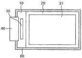
도 1은 본 발명에 따른, 휴대 전화 등에 사용되는 액정 표시 패널의 평면도이다. 도 1에서, TFT 기판(10) 위에 컬러 필터 기판(20)이 설치되어 있다. TFT 기판(10)과 컬러 필터 기판(20) 사이에 도시하지 않은 액정층이 협지되어 있다. TFT 기판(10)과 컬러 필터 기판(20)와는 액연부에 형성된 도시하지 않은 시일재에 의해 접착되어 있다. TFT 기판(10)은 컬러 필터 기판(20)보다도 크게 형성되어 있고, TFT 기판(10)이 컬러 필터 기판(20)보다도 크게 되어 있는 부분에는, 액정 표시 패널에 전원, 영상 신호, 주사 신호 등을 공급하기 위한 단자부가 형성되어 있다.1 is a plan view of a liquid crystal display panel used in a mobile telephone or the like according to the present invention. In FIG. 1, a
단자부에는, 주사선, 영상 신호선 등을 구동하기 위한 IC 드라이버(30)가 설치되어 있다. IC 드라이버(30)에는 주사선 구동 회로, 영상 신호선 구동 회로가 형성되어 있다. IC 드라이버(30)에는, 단자부에 접속한 메인 플렉시블 배선 기판(40)을 통하여, 주사 신호, 영상 신호가 공급된다.In the terminal portion, an
TFT 기판(10)의 상측에는, 상부 편광판(21)이 접착되어 있다. 상부 편광판(21)의 외형은 표시 영역과 거의 동등하다. 즉, 액정은 편광광만을 제어할 수 있으므로, TFT 기판(10)의 하측에 하부 편광판을 접착하고, 백라이트로부터의 광을 직선편광으로 편광한다. 이 직선 편광광이 액정층에 의해 변조를 받아, 화소마다 투과율이 변화하는 것에 의해 화상이 형성된다. 그리고, 상부 편광판(21)에 의해 다시 편광(광 검출)하는 것에 의해 인간의 눈에 화상이 시인된다.The upper
액정 표시 패널 전체는, 틀 형상의 수지 몰드(60) 내에 수용되어 있다. 수지 몰드(60) 내의 액정 표시 패널의 하측에는 이후에 설명하는 백라이트가 수용되어 있다. 도 1에서, 액정 표시 패널의 단자부에 접속되어 있는 메인 플렉시블 배선 기판(40)은 수지 몰드(60)의 단부에서 구부려져 배면으로 연장되어 있다. 이에 의해, 액정 표시 장치의 외형을 작게 하고 있다.The whole liquid crystal display panel is accommodated in the frame-shaped
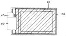
도 2는 도 1에서 설명한 액정 표시 패널에 대해 터치 패널(100)을 접착한 도면이다. 터치 패널(100)은 액정 표시 패널의 컬러 필터 기판(20)보다도 약간 크게 형성되고, 수지 몰드(60)의 일부도 덮여 있다. 도 2에서, 터치 패널(100)에 전원이나 신호를 공급하는 터치 패널용 플렉시블 배선 기판(50)이 터치 패널(100)의 단부에 부착되어 있다. 이 터치 패널용 플렉시블 배선 기판(50)도 몰드의 단부에서 배면으로 구부려져 휘어지는 것에 의해 액정 표시 장치의 외형을 작게 하고 있다. 또한, 배면에서 메인 플렉시블 배선 기판(40)과 터치 패널용 플렉시블 배선 기판(50)은 접속되어 있다.FIG. 2 is a diagram in which the
터치 패널 기판은 일반적으로는 글래스로 형성되지만, 투명하며, ITO의 어닐링 등의 온도에 견딜 수 있으면 플라스틱 기판이어도 된다. 투명 수지로서는, 예를 들면, 아크릴, 폴리카보네이트 등을 사용할 수 있다.The touch panel substrate is generally formed of glass, but may be transparent, and may be a plastic substrate as long as it can withstand temperatures such as annealing of ITO. As transparent resin, acryl, polycarbonate, etc. can be used, for example.
터치 패널(100)의 기판은 액정 표시 패널의 컬러 필터 기판(20)에 접착재에 의해 부착된다. 접착재로서는, 예를 들면, 아크릴 수지계의 UV 경화 수지(110)가 사용된다. UV 경화 수지(110)는 당초는 액체이며, 액정 표시 패널과 터치 패널(100)을 접착할 때는 감압 분위기 속에서 행해져, 기포의 혼입을 방지한다.The substrate of the
경화된 후의 UV 경화 수지(110)는 열 가소성이다. 즉, 완성 후, 터치 패널(100)과 액정 표시 패널 사이에 기포, 이물질 등의 불량이 발견된 경우에, 터치 패널(100)을 액정 표시 패널로부터 잡아 당겨 재생하기 위해서이다. 또한, 컬러 필터 기판(20)과 터치 패널(100)과의 접착에는 점착재 시트를 이용할 수도 있다. 이 경우의 점착재 시트도 열 가소성인 것이 바람직하다.The UV cured
도 3은 도 2에서 형성된 액정 표시 패널에 터치 패널(100)을 부착한 상태의 것에 대해 프론트 윈도우(200)를 부착한 상태를 도시한다. 프론트 윈도우(200)는 일반적으로는 글래스가 이용되고, 두께는 0.5㎜ 정도이다. 프론트 윈도우(200)의 재료로는 아크릴 수지, 폴리카보네이트 수지 등의 플라스틱을 이용할 수도 있다.3 illustrates a state in which the
프론트 윈도우(200)의 부착은, 터치 패널(100)과 프론트 윈도우(200) 사이에 점착재 시트(210)를 배치하여 접착한다. 이 경우, 작업의 용이성으로부터 프론트 윈도우(200)측에 점착재 시트(210)를 형성한다. 또한, 이 경우의 점착재 시트(210)도, 액정 표시 패널과 터치 패널(100) 사이에 형성하는 UV 경화 수지(110)의 경우와 마찬가지로, 재생을 고려하여, 열 가소성의 점착재 시트가 사용된다.Attachment of the
도 3에서, 프론트 윈도우(200)의 외형은 액정 표시 패널 및 수지 몰드(60)보다도 크고, 액정 표시 패널 등 전체를 보호하고 있다. 또한, 프론트 윈도우(200)는 TFT 기판(10)에 부착된 메인 플렉시블 배선 기판(40), 터치 패널(100)에 부착된 터치 패널용 플렉시블 배선 기판(50)도 덮어 보호하고 있다.In FIG. 3, the outer shape of the
도 3에서, 로고 마크(80)가 프론트 윈도우(200)의 이면측의 주변에 배치되어 있다. 로고 마크(80)는 터치 패널용 플렉시블 배선 기판(50)과 겹치는 위치에 배치되어 있다.In FIG. 3, the
도 4는 도 3의 A-A 단면도이다. 본 명세서에서는, TFT 기판(10)과 컬러 필터 기판(20)을 조합한 것을 액정 셀이라고 부르고, 액정 셀에 하부 편광판(11)과 상부 편광판(21)을 접착한 것을 액정 표시 패널이라고 부른다. 컬러 필터 기판(20)에 접착한 상부 편광판(21)에 UV 경화 수지(110)를 통하여 터치 패널(100)이 접착되어 있다.4 is a cross-sectional view taken along the line A-A of FIG. In this specification, the combination of the
터치 패널(100) 위에는 프론트 윈도우(200)가 점착재 시트(210)를 통하여 접착되어 있다. 프론트 윈도우(200)가 폴리카보네이트, 아크릴 등 플라스틱으로 형성되는 경우도 있다. 프론트 윈도우(200)의 외형은 크고, 터치 패널용 플렉시블 배선 기판(50) 및 메인 플렉시블 배선 기판(40)도 덮여 있다.The
터치 패널(100)에는 터치 패널용 플렉시블 배선 기판(50)이 접속되어 있다. 터치 패널용 플렉시블 배선 기판(50)에는 터치 패널(100)용 전자 부품(51)이 배치되어 있지만 이 터치 패널(100)용 전자 부품(51)은 플렉시블 배선 기판의 하측에 배치하고 있다.The touch panel
도 4에서, 액정 셀의 TFT 기판(10)의 단자부에는 IC 드라이버(30)가 배치되어 있다. 또한 TFT 기판(10)에 형성된 단자에는 메인 플렉시블 배선 기판(40)이 접속되어 있다. 메인 플렉시블 배선 기판(40)은 구부려져 액정 표시 패널의 배면으로 연장되어 있다.In FIG. 4, the
메인 플렉시블 배선 기판(40)에는, LCD용 전자 부품(41)이 부착되어 있다. 도 4에서, 프론트 윈도우(200)는 메인 플렉시블 배선 기판(40)에 부착된 LCD용 전자 부품(41)도 덮도록 설정되어 있다. 또한, 전자 부품은 도 4와 같이, 반드시 전자 부품이 하향으로 되도록 배치할 필요는 없으며, 레이아웃에 따라서 전자 부품이 상향되도록, 플렉시블 배선 기판이 백라이트의 배면으로 연장되는 부분에 배치하여도 된다.The LCD
도 4에서는, 전자 부품을 메인 플렉시블 배선 기판(40)의 하측에 배치함과 함께, 발광 다이오드(70)도 다른 전자 부품과 마찬가지로 메인 플렉시블 배선 기판(40)의 하측에 배치한다. 단, 발광 다이오드(70)는 메인 플렉시블 배선 기판(40)이 수지 몰드(60)의 배면으로 구부려진 부분에 배치된다. 그렇게 하면, 메인 플렉시블 배선 기판(40)을 배면으로 구부렸을 때, 수지 몰드(60)에 형성된 오목부에 발광 다이오드(70)를 수용할 수 있다. 그리고 발광 다이오드(70)는 도 4에 도시한 바와 같이, 도광판(62)의 단부와 대향하여 배치되어, 백라이트의 일부로 된다. 또한, 발광 다이오드(70)에는 본 실시예에서는, 백색 발광 다이오드(70)가 사용된다.In FIG. 4, the electronic component is disposed below the main
도 4에서, 액정 표시 패널은 수지 몰드(60)에 재치되어 있다. 수지 몰드(60)는 사각의 틀 형상으로 되어 있다. 도 4에서, 액정 표시 패널 하부 편광판(11)은 수지 몰드(60) 내에 수용되고, 하부 편광판(11)의 배면에는 백라이트가 배치되어 있다. 백라이트는 다음과 같은 구성으로 되어 있다.In FIG. 4, the liquid crystal display panel is mounted on the
단부가 발광 다이오드(70)와 대향한 도광판(62)이 배치되어 있다. 도광판(62)의 역할은 측면으로부터 입사하는 발광 다이오드(70)로부터의 광을 액정 표시 패널측을 향하게 하는 것이다. 발광 다이오드(70)는 사이즈가 크므로, 액정 표시 장치 전체의 두께를 작게 하기 위해, 도광판(62)은 발광 다이오드(70)와 대향하는 부분에서, 높이를 높게 하고, 이후에 설명하는 광학 시트와 겹치는 부분에서, 두께를 작게 하고 있다.The
도 4에서, 도광판(62)의 하측에는 반사 시트(61)가 배치되어 있다. 도광판(62)으로부터 하측을 향하는 광을 반사하여 액정 표시 패널측을 향하게 하기 위해서이다. 한편, 도광판(62)의 상측에는 도 5에 도시한 바와 같은, 하부 확산 시트(63), 하부 프리즘 시트(64), 상부 프리즘 시트(65), 상부 확산 시트(66)로 이루어지는 광학 시트군(67)이 배치되어 있다.In FIG. 4, a
도 5는 광학 시트군(67)의 분해 사시도이다. 도 5에서, 하부 확산 시트(63)는 밝기 불균일을 경감하는 역할을 갖고 있다. 하부 프리즘 시트(64)는 a 방향으로 펴지게 하고자 하는 백라이트로부터 광을 액정 표시 패널의 방향을 향하고, 상부 프리즘 시트(65)는 b 방향으로 펴지게 하고자 하는 백라이트로부터의 광을 액정 표시 패널의 방향을 향하게 하는 역할을 갖는다. 상부 확산 시트(66)의 역할은 주로, 하부 프리즘 시트(64) 혹은 상부 프리즘 시트(65)와 액정 표시 패널과의 사이에서 발생하는 므와레 형상을 경감하는 역할을 갖는다.5 is an exploded perspective view of the
도 4를 다시 참조하면, 이들 광학 시트군(67)은 도광판(62) 위에 겹쳐진다. 광학 시트군(67)의 가장 위의 상부 확산 시트(66)와 액정 표시 패널 하부 편광판(11) 사이에는 50㎛ 정도의 간격이 비워져 있다. 하부 편광판(11)과 상부 확산 시트(66)가 마찰되어 손상이 발생하는 것을 방지하기 위해서이다.Referring again to FIG. 4, these
도 4에서, 액정 셀에 접속한 메인 플렉시블 배선 기판(40)과, 터치 패널(100)에 접속한 터치 패널용 플렉시블 배선 기판(50)은 구부려져 액정 표시 패널의 배면으로 연장되어 있다. 메인 플렉시블 배선 기판(40)과 터치 패널용 플렉시블 배선 기판(50)은 도 4에는 도시하지 않은 장소에서 접속된다.In FIG. 4, the main
도 4에서, 프론트 윈도우(200)의 이면측에서, 점착재 시트(210)가 존재하고 있지 않은 부분에 로고 마크(80)가 인쇄에 의해 형성되어 있다. 로고 마크(80)는 터치 패널용 플렉시블 배선 기판(50)과 겹치는 위치에 배치되어 있다. 로고 마크(80)는 복수의 층으로 형성되어 있지만, 도 4에 도시한 로고 마크(80)의 위치는 복수층의 부분이다.In FIG. 4, the
도 6은 로고 마크(80)의 형성 방법을 도시하는 도면이다. 로고 마크(80)는 인쇄에 의해 형성된다. 도 6에서는, 로고 마크(80)는 2층으로 형성되어 있다. 제1층(81)은 흑색의 수지이며, 표시하고자 하는 마크, 도 6에서는 A, B, C, D를 뺀 것을 인쇄에 의해 형성한다. 도 6의 (a)는 표면측에서 본 도면이며, 도 6의 (b)는 이면측에서 본 도면이다. 인쇄의 패턴은 도 6의 (b)와 같이 되어 있다. 도 6의 (e)는 로고 마크(80)의 제1층(81)을 인쇄한 상태를 도시하는 단면도이다.6 is a diagram illustrating a method of forming the
로고 마크(80)는 백색 혹은 소정의 색으로 표시한다. 이것은, 제2층(82)을 제1층(81)에 대해 겹쳐 도포함으로써 행해진다. 도 6의 (c)는 제2층(82)을 겹쳐 도포한 상태를 프론트 윈도우(200)의 이면측으로부터 본 도면이다. 도 6의 (c)에 도시한 바와 같이, 제2층(82)은, 제1층(81)의 일부에 대해 겹쳐 도포된다.The
도 6의 (f)는 도 6의 (c)의 단면도이다. 도 6의 (f)에서, 제2층(82)이 제1층(81)의 창부를 덮고, 제2층(82)에 의해 로고 마크(80)의 색을 정하고 있다. 제2층(82)은, 수지에 백색 혹은 소정의 색의 안료가 분산되어 있는 것이다. 도 6의 (d)는 이와 같이 하여 형성된 로고 마크(80)를 프론트 윈도우(200)의 표면측에서 본 도면이다.(F) of FIG. 6 is sectional drawing of (c) of FIG. In FIG. 6F, the
로고 마크(80)는 외측으로부터의 반사광에 의해 시인되는 것을 상정하고 있다. 한편, 도 4에 도시한 바와 같이, 휴대 전화 등에 사용되는 소형의 액정 표시 장치에서는, 백라이트의 광원으로서 발광 다이오드가 사용되고 있다. 발광 다이오드는 고휘도로 발광할 필요가 있다. 발광 다이오드로부터의 광은, 수지 몰드(60) 혹은 광학 부품 사이로부터 누설되어 일부가 로고 마크(80)의 하부에 도달한다. 발광 다이오드로부터의 광이 로고 마크(80)에 영향을 미치면, 로고 마크(80)가 소정의 시인성을 얻을 수 없는 경우가 있다.It is assumed that the
로고 마크(80)의 색 등의 시인성에 대해 발광 다이오드로부터의 광의 영향을 없애기 위해서는, 로고 마크(80)의 부분에서, 발광 다이오드로부터의 광을 차광하거나, 로고 마크(80)의 제2층(82)을 두껍게 할 필요가 있다. 본 실시예에서는, 제2층(82)을 두껍게 하여 발광 다이오드로부터의 광의 영향을 제거하고 있다.In order to eliminate the influence of the light from the light emitting diode on the visibility of the color of the
도 6의 (f)에서, 로고 마크(80)의 제1층(81)은 10㎛ 정도이지만, 제2층(82)은 15㎛ 정도 혹은 그 이상으로 하고 있다. 그렇게 하면, 로고 마크(80)의 제2층(82) 부분의 두께 d2가 25㎛ 이상으로 된다. 휴대 전화 등에 사용되는 액정 표시 장치는 얇게 하는 것이 요구되어 있으므로, 로고 마크(80)의 두께가 커지면, 문제가 생기는 경우가 있다.In FIG. 6F, the
도 7은 도 4에 도시한 액정 표시 장치의 로고 마크(80) 부근에서의 상세 단면도이다. 도 7에서, 점착재 시트(210)의 두께 d1은 예를 들면, 100㎛이다. 로고 마크(80)의 2층부에서의 두께 d2는 예를 들면, 25㎛이다. 터치 패널용 플렉시블 배선 기판(50)의 두께는 70㎛ 정도이다. 도 7에서는, 점착재 시트(210)의 두께 d1은 간신히 로고 마크(80)의 두께 d2와 터치 패널용 플렉시블 배선 기판(50)의 두께 d3의 합계보다도 크다.FIG. 7 is a detailed sectional view in the vicinity of the
그러나, 부품의 두께의 변동을 고려하면, d1이 d2와 d3의 합계보다도 작아지는 경우, 즉, d1<d2+d3도 있을 수 있다. 또한, 액정 표시 장치에 대해서는 박형화의 요구가 항상 있으므로, 점착재 시트(210)의 두께를 더 작게 하는 것도 예상된다. 그렇게 하면, d1<d2+d3으로 되는 것이 상태화(常態化)하는 것도 상정된다.However, in consideration of the variation in the thickness of the component, there may be a case where d1 becomes smaller than the sum of d2 and d3, that is, d1 <d2 + d3. In addition, since there is always a demand for thinning of the liquid crystal display device, it is also expected to make the thickness of the pressure-
d1<d2+d3인 경우, 로고 마크(80)가 프론트 윈도우(200), 터치 패널용 플렉시블 배선 기판(50), 터치 패널(100)과의 겹친 부분에 배치되어 있으면, 점착재 시트(210)에 의해 접착되어 있는 프론트 윈도우(200)와 터치 패널(100)을 잡아 당기는 응력이 발생한다. 또한, 도 7에서, 로고 마크(80)의 제1층(81)은 점착재 시트(210) 아래에 들어가 있지만, 이 부분에서는 점착재 시트(210)가 찌부러져 두께가 작아져 있다. 따라서, 두께를 비교하는 경우는, 점착재 시트(210)의 두께 d1과 다른 두께를 비교하면 된다.When d1 <d2 + d3, if the
본 발명에서는, 로고 마크(80)의 위치를 터치 패널용 플렉시블 배선 기판(50)과는 겹치지만, 터치 패널(100)과는 겹치지 않는 위치에 배치함으로써, 프론트 윈도우(200)와 터치 패널(100)을 잡아 당기는 응력의 발생을 방지하고 있다. 즉, 도 7에서, 로고 마크(80)의 제2층(82)의 단부와 터치 패널(100)의 단부와의 거리 L을 0 이상으로 하고 있다.In this invention, the
이와 같은 구성으로 함으로써, 만약, 로고 마크(80)와 터치 패널용 플렉시블 배선 기판(50)의 두께의 합계가 점착재 시트(210)의 두께보다도 커졌다고 하여도, 터치 패널용 플렉시블 배선 기판(50)이 하측으로 움직일 수 있으므로, 점착재 시트(210)에 잡아 당기는 응력이 가해지는 일은 없다. 따라서, 신뢰성이 높은 액정 표시 장치를 실현할 수 있다.By setting it as such a structure, even if the sum total of the thickness of the
<실시예 2><Example 2>
프론트 윈도우(200)의 이면에 형성된 로고 마크(80)에 백라이트의 발광 다이오드로부터의 광이 입사하면 로고 마크(80)의 색 등에, 소정의 디자인성이 얻어지지 않는 경우가 있다. 이를 방지하기 위해 실시예 1에서는, 로고 마크(80)의 제2층(82)을 두껍게 함으로써 대처하고 있다. 그러나, 실시예 1에서는 충분한 차광 효과가 얻어지지 않는 경우도 있을 수 있다. 본 실시예는, 로고 마크(80)에 백색 또는 소정의 색을 형성하기 위한 제2층(82) 위에 차광막인 제3층(83)을 더 형성함으로써, 발광 다이오드로부터의 광의 영향을 방지하고 있다.When light from a light emitting diode of a backlight enters into the
도 8은 본 실시예에서의 로고 마크(80)를 형성하는 프로세스를 도시하는 단면도이다. 도 8의 (a)는 제1층(81)을 프론트 윈도우(200)의 이면에 형성한 도면이며, 도 8의 (b)는 제2층(82)을 형성한 도면이며, 도 8의 (c)는 제3층(83)을 형성한 도면이다. 제1층(81)의 두께는 10㎛ 정도이며, 제2층(82)의 두께는 10㎛ 정도, 제3층(83)의 두께도 10㎛ 정도이다.8 is a cross-sectional view showing a process of forming the
본 실시예에서는, 차광막인 제3층(83)이 형성되어 있는 만큼, 제2층(82)의 두께는 실시예 1의 경우보다도 작아져 있다. 제2층(82)은 수지로 형성되고, 백색 혹은 소정의 색의 안료가 분산되어 있다. 차광막인 제3층(83)은 흑색이며, 에폭시 등의 유기 수지에 흑색의 안료가 분산되어 있다.In the present embodiment, the thickness of the
차광을 완전하게 하기 위해, 제3층(83)은 제2층(82)의 측부도 덮여 있다. 도 8의 (c)에서, 제1층(81)에서 제3층(83)까지의 두께의 합계 d2는 예를 들면, 30㎛ 정도이다. 점착재 시트(210)의 두께, 및, 터치 패널용 플렉시블 배선 기판(50)의 두께와의 관계에서는, 도 8의 (c)에서의 로고 마크(80)의 두께 d2가 문제로 된다.In order to complete shading, the
도 9는 3층으로 되어 있는 로고 마크(80)가 프론트 윈도우(200)의 이면에 형성되어 있는 경우의 단면도이다. 도 9에서, 점착재 시트(210)의 두께 d1은 100㎛, 터치 패널용 플렉시블 배선 기판(50)의 두께 d3은 70㎛, 로고 마크(80)의 3층 부분의 두께 d2는 30㎛이다. 부품의 제조 공차를 고려하면, 반수(半數)는 d1<d2+d3으로 된다.9 is a cross-sectional view when the
도 9에서는, 로고 마크(80)의 제3층(83)의 단부는 터치 패널(100)의 단부보다도 외측에 형성되어 있다. 즉, 도 9의 L은 제로보다도 크다. 따라서, d1<d2+d3의 관계로 되었다고 하여도 터치 패널용 플렉시블 배선 기판(50)이 하측으로 움직일 수 있기 때문에 프론트 윈도우(200)와 터치 패널(100)과의 사이의 점착재 시트(210)의 잡아 당기는 응력이 생기는 일은 없다.In FIG. 9, the end portion of the
도 9의 L은 평면에서 본 경우의, 제2층(82)의 단부와 터치 패널(100)의 단부와의 거리이다. 다시 말해서, 로고 마크(80)에서, 3층 구성으로 되어 있는 부분의 단부와 터치 패널(100)의 단부와의 거리가 L이다.L in FIG. 9 is a distance between the end of the
이와 같이, 로고 마크(80)를 3층으로 형성하여도, 본 실시예의 구성에 따르면, 프론트 윈도우(200)와 터치 패널용 플렉시블 배선 기판(50)의 잡아 당기는 응력은 발생하지 않는다. 따라서, 액정 표시 장치의 신뢰성의 저하를 방지할 수 있다.Thus, even if the
<실시예 3><Example 3>
실시예 1에서는, 로고 마크(80)의 제2층(82)과 터치 패널(100)의 단부의 거리 L을 제로보다도 크게 하고, 실시예 2에서는, 로고 마크(80)의 3층 구조로 되어 있는 부분의 단부와 터치 패널(100)의 단부의 거리 L을 제로보다도 크게 하고 있다. 거리 L이 제로 부근에서는, 휨 응력이 크므로, 도 7 등에서, d1<d2+d3으로 된 경우, 프론트 윈도우(200)와 터치 패널용 플렉시블 배선 기판(50)과의 사이의 점착재 시트(210)에 대한 잡아 당기는 응력이 존재하는 경우가 있을 수 있다.In Example 1, the distance L between the
본 실시예는 이에 대한 대책이다. 도 10은 본 실시예에서의, 프론트 윈도우(200)의 이면에 형성된 로고 마크(80) 부근의 상세 단면도이다. 도 10에서, 터치 패널(100)보다 아래의 구성은 생략되어 있다.This embodiment is a countermeasure against this. 10 is a detailed sectional view of the vicinity of the
도 10에서, 터치 패널(100)에는 터치 패널용 플렉시블 배선 기판(50)이 부착되어 있다. 터치 패널용 플렉시블 배선 기판(50)은 기재(52) 위에 구리 배선(53)이 형성되고, 구리 배선(53)을 오버코트(54)막이 덮여 있는 구성으로 되어 있다. 터치 패널용 플렉시블 배선 기판(50)이 터치 패널(100)과 접속되어 있는 부분은, 오버코트(54)가 존재하지 않고, Ni층(55), Au층(56)이 형성되어 있다.In FIG. 10, a touch panel
도 10에서의 각 부재의 두께는 예를 들면 다음과 같이 되어 있다. 터치 패널용 플렉시블 배선 기판(50)의 기재(52)의 두께는 40㎛, 구리 배선(53)의 두께는 20㎛, 오버코트(54)의 두께는 25㎛, 단자부에서의 Ni층(55)의 두께는 1㎛ 내지 5㎛, Au층(56)의 두께는 0.03∼0.3㎛이다. Ni층(55) 및 Au층(56)은 오버코트(54)가 형성되어 있는 부분에는 존재하지 않는다. 도 10에서, 터치 패널용 플렉시블 배선 기판(50)을 점착재 시트(210)의 두께 d1, 로고 마크(80)의 두께 d2와 비교하는 경우의 두께는 오버코트(54)가 없는 부분의 두께 d3으로 된다.The thickness of each member in FIG. 10 is as follows, for example. The thickness of the
도 10에서의 로고 마크(80)의 두께는 실시예 1의 경우와 마찬가지로, 제1층(81)은 10㎛, 제2층(82)은 15㎛이다. 또한, 점착재 시트(210)의 두께 d1은 100㎛이다. 단, 이들 부품의 두께는 변동되는 경우가 많다. 도 10에서는, L을 0.3㎜ 이상으로 함으로써, d1<d2+d3의 관계가 생겼다고 하여도, L의 값을 0.3 이상으로 하고 있으므로, 점착재 시트(210)에 가해지는 잡아 당기는 응력은 매우 작게 억제할 수 있다.The thickness of the
도 10에서, 터치 패널용 플렉시블 배선 기판(50)의 오버코트(54)의 단부와 터치 패널(100)의 단부의 거리 M이 극단적으로 작아진 경우, 터치 패널용 플렉시블 배선 기판(50)의 휨 응력이 커진다. 그러나, 본 실시예에서는, 로고 마크(80)의 제2층(82)의 단부와 터치 패널(100)의 단부의 거리 L이 0.3㎜ 이상이므로, 터치 패널용 플렉시블 배선 기판(50)의 휨 응력을 작게 억제할 수 있어, 휨 응력에 의한 점착재 시트(210)의 잡아 당기는 응력을 억제할 수 있다.In FIG. 10, when the distance M between the end of the
도 10에서는, 로고 마크(80)가 2층인 경우에 대해 설명하였지만, 로고 마크(80)가 실시예 2와 같이 3층으로 형성되는 경우도 마찬가지이다.Although the case where the
10 : TFT 기판
11 : 하부 편광판
20 : 컬러 필터 기판
21 : 상부 편광판
30 : IC 드라이버
40 : 메인 플렉시블 배선 기판
41 : 액정 표시 장치용 전자 부품
50 : 터치 패널용 플렉시블 배선 기판
51 : 터치 패널용 전자 부품
52 : 기재
53 : 구리 배선
54 : 오버코트
55 : Ni층
56 : Au층
60 : 수지 몰드
61 : 반사 시트
62 : 도광판
63 : 하부 확산 시트
64 : 하부 프리즘 시트
65 : 상부 프리즘 시트
66 : 상부 확산 시트
67 : 광학 시트군
70 : 발광 다이오드
80 : 로고 마크
81 : 제1층
82 : 제2층
83 : 제3층
100 : 터치 패널
110 : UV 경화 수지
150 : 표시 영역
200 : 프론트 윈도우
210 : 점착재 시트10: TFT substrate
11: lower polarizer
20: color filter substrate
21: upper polarizer
30: IC driver
40: main flexible wiring board
41 electronic component for liquid crystal display device
50: flexible wiring board for touch panel
51: electronic components for the touch panel
52: description
53: copper wiring
54: overcoat
55: Ni layer
56: Au layer
60: resin mold
61: reflective sheet
62: light guide plate
63: lower diffusion sheet
64: lower prism sheet
65: upper prism sheet
66: upper diffusion sheet
67: optical sheet group
70: light emitting diode
80: logo mark
81: first floor
82: second layer
83: third layer
100: touch panel
110: UV Curing Resin
150: display area
200: front window
210: adhesive sheet
Claims (5)
Translated fromKorean상기 터치 패널과 상기 프론트 윈도우는 점착재 시트에 의해 접착되고,
상기 터치 패널의 특정한 변에는 터치 패널용 플렉시블 배선 기판이 접속되고,
상기 프론트 윈도우의 상기 터치 패널측의 면에는 복수층으로 형성된 로고 마크가 형성되고, 상기 로고 마크가 복수층으로 되어 있는 부분은 상기 점착재 시트의 외측에 배치되고, 상기 복수층의 단부와 상기 터치 패널과의 평면에서 본 거리는 제로보다 큰 것을 특징으로 하는 액정 표시 장치.A liquid crystal display panel and a backlight are accommodated in a resin mold, a touch panel is adhered on the liquid crystal display panel, and a front window is adhered to the touch panel.
The touch panel and the front window are bonded by an adhesive sheet,
To a specific side of the touch panel, a flexible wiring board for a touch panel is connected,
A logo mark formed of a plurality of layers is formed on the surface of the front panel of the front window, and a portion where the logo mark is formed of a plurality of layers is disposed outside the pressure-sensitive adhesive sheet, and the ends of the plurality of layers and the touch are formed. A liquid crystal display device characterized in that the distance seen from the plane with the panel is greater than zero.
상기 점착재 시트의 두께를 d1, 상기 로고 마크의 상기 복수층으로 되어 있는 부분의 두께를 d2, 상기 터치 패널용 플렉시블 배선 기판의 두께를 d3으로 한 경우, d1<d2+d3의 관계로 되어 있는 것을 특징으로 하는 액정 표시 장치.The method of claim 1,
When the thickness of the said adhesive material sheet is d1, the thickness of the part which becomes the said multiple layer of the said logo mark is d2, and the thickness of the said flexible wiring board for touch panels is d3, it has a relationship of d1 <d2 + d3. A liquid crystal display device, characterized in that.
상기 복수층의 단부와 상기 터치 패널과의 평면에서 본 거리는 0.3㎜보다 큰 것을 특징으로 하는 액정 표시 장치.The method of claim 1,
A plane view distance between the end portions of the plurality of layers and the touch panel is greater than 0.3 mm.
상기 터치 패널과 상기 프론트 윈도우는 점착재 시트에 의해 접착되고,
상기 터치 패널의 특정한 변에는 터치 패널용 플렉시블 배선 기판이 접속되고,
상기 프론트 윈도우의 상기 터치 패널측의 면에는 상기 프론트 윈도우의 측으로부터 제1층, 제2층의, 2층으로 형성된 로고 마크가 형성되고, 상기 로고 마크가 2층으로 되어 있는 부분은 상기 점착재 시트의 외측에 배치되고, 상기 로고 마크의 상기 제2층의 단부와 상기 터치 패널의 단부와의 평면에서 본 거리는 제로보다 큰 것을 특징으로 하는 액정 표시 장치.A liquid crystal display panel and a backlight are accommodated in a resin mold, a touch panel is adhered on the liquid crystal display panel, and a front window is adhered to the touch panel.
The touch panel and the front window are bonded by an adhesive sheet,
To a specific side of the touch panel, a flexible wiring board for a touch panel is connected,
On the surface of the front window of the front window, a logo mark formed of two layers of first and second layers is formed from the front window side, and the portion of the logo mark having two layers is the adhesive material. It is arrange | positioned on the outer side of a sheet | seat, The liquid crystal display device characterized by the distance seen from the plane of the edge part of the said 2nd layer of the said logo mark, and the edge part of the said touch panel larger than zero.
상기 터치 패널과 상기 프론트 윈도우는 점착재 시트에 의해 접착되고,
상기 터치 패널의 특정한 변에는 터치 패널용 플렉시블 배선 기판이 접속되고,
상기 프론트 윈도우의 상기 터치 패널측의 면에는 상기 프론트 윈도우의 측으로부터 제1층, 제2층, 제3층의, 3층으로 형성된 로고 마크가 형성되고, 상기 제2층의 단부는 상기 제3층에 의해 덮여지고,
상기 로고 마크가 3층으로 되어 있는 부분은 상기 점착재 시트의 외측에 배치되고, 상기 로고 마크의 상기 제2층의 단부와 상기 터치 패널의 단부와의 평면에서 본 거리는 제로보다 큰 것을 특징으로 하는 액정 표시 장치.A liquid crystal display panel and a backlight are accommodated in a resin mold, a touch panel is adhered on the liquid crystal display panel, and a front window is adhered to the touch panel.
The touch panel and the front window are bonded by an adhesive sheet,
To a specific side of the touch panel, a flexible wiring board for a touch panel is connected,
A logo mark formed of three layers of a first layer, a second layer, and a third layer is formed on a surface of the front window on the touch panel side, and an end of the second layer is formed on the third layer. Being covered by floors,
The portion where the logo mark has three layers is disposed outside the pressure-sensitive adhesive sheet, and the distance in plan view between the end portion of the second layer of the logo mark and the end portion of the touch panel is greater than zero. Liquid crystal display.
Applications Claiming Priority (2)
| Application Number | Priority Date | Filing Date | Title |
|---|---|---|---|
| JP2009107678AJP5235769B2 (en) | 2009-04-27 | 2009-04-27 | Liquid crystal display |
| JPJP-P-2009-107678 | 2009-04-27 |
Publications (2)
| Publication Number | Publication Date |
|---|---|
| KR20100118081Atrue KR20100118081A (en) | 2010-11-04 |
| KR101212345B1 KR101212345B1 (en) | 2012-12-13 |
Family
ID=42321096
Family Applications (1)
| Application Number | Title | Priority Date | Filing Date |
|---|---|---|---|
| KR1020100038666AExpired - Fee RelatedKR101212345B1 (en) | 2009-04-27 | 2010-04-26 | Liquid crystal display device |
Country Status (6)
| Country | Link |
|---|---|
| US (6) | US8581862B2 (en) |
| EP (1) | EP2246730B1 (en) |
| JP (1) | JP5235769B2 (en) |
| KR (1) | KR101212345B1 (en) |
| CN (1) | CN101872084B (en) |
| TW (1) | TWI490592B (en) |
Cited By (2)
| Publication number | Priority date | Publication date | Assignee | Title |
|---|---|---|---|---|
| KR101490172B1 (en)* | 2013-06-05 | 2015-02-05 | 주식회사 라온이노텍 | Transparent member having an image and method for forming the image on the transparent member |
| US9436302B2 (en) | 2012-07-25 | 2016-09-06 | Samsung Display Co., Ltd. | Display device including touch emitting key unit |
Families Citing this family (46)
| Publication number | Priority date | Publication date | Assignee | Title |
|---|---|---|---|---|
| JP5235769B2 (en)* | 2009-04-27 | 2013-07-10 | 株式会社ジャパンディスプレイイースト | Liquid crystal display |
| US20130018489A1 (en)* | 2011-07-14 | 2013-01-17 | Grunthaner Martin Paul | Combined force and proximity sensing |
| CN102955598A (en)* | 2011-08-25 | 2013-03-06 | 联胜(中国)科技有限公司 | Touch panel and touch display device |
| JP5814703B2 (en)* | 2011-09-01 | 2015-11-17 | アルプス電気株式会社 | Input device and manufacturing method thereof |
| JPWO2013035276A1 (en)* | 2011-09-06 | 2015-03-23 | 凸版印刷株式会社 | Integrated touch sensor substrate, display device including the same, and method for manufacturing the integrated touch sensor substrate |
| CN102999200A (en)* | 2011-09-18 | 2013-03-27 | 宸鸿科技(厦门)有限公司 | Touch display device and manufacturing method thereof |
| KR101357592B1 (en)* | 2011-09-28 | 2014-02-04 | 엘지이노텍 주식회사 | Touch-Window |
| FR2985076B1 (en)* | 2011-12-23 | 2014-08-29 | Valeo Systemes Thermiques | CONTROL AND DISPLAY MODULE FOR A MOTOR VEHICLE AND METHOD FOR MANUFACTURING THE SAME |
| CN103176641A (en)* | 2011-12-25 | 2013-06-26 | 宸鸿科技(厦门)有限公司 | Touch panel and manufacturing method thereof |
| JP6086278B2 (en)* | 2012-02-20 | 2017-03-01 | 大日本印刷株式会社 | Front protective plate for display device with wiring, manufacturing method thereof, and display device |
| JP6415798B2 (en)* | 2012-04-05 | 2018-10-31 | 大日本印刷株式会社 | Front protective plate for display device and display device |
| KR101946463B1 (en) | 2012-07-27 | 2019-02-12 | 삼성디스플레이 주식회사 | Laminating apparatus and laminating method |
| US20140098332A1 (en)* | 2012-10-10 | 2014-04-10 | Apple Inc. | Displays With Logos and Alignment Marks |
| KR102035005B1 (en)* | 2012-12-24 | 2019-10-22 | 엘지디스플레이 주식회사 | Touch display device |
| CN104123022B (en)* | 2013-04-24 | 2017-07-28 | 宸鸿科技(厦门)有限公司 | Contact panel and its covering plate structure |
| US20140353020A1 (en)* | 2013-05-30 | 2014-12-04 | Tianjin Funayuanchuang Technology Co., Ltd. | Touch panel |
| TWI562030B (en)* | 2013-07-02 | 2016-12-11 | Touch panel structure, method for forming touch panel structure and touch device thereof | |
| TWI515617B (en)* | 2013-08-07 | 2016-01-01 | 達鴻先進科技股份有限公司 | Touch panel structure and method for forming the same |
| JP2015041021A (en)* | 2013-08-23 | 2015-03-02 | 大日本印刷株式会社 | Front protective plate for display device and display device |
| KR102107564B1 (en) | 2013-11-06 | 2020-05-08 | 삼성디스플레이 주식회사 | Liquid crystal device |
| US9638950B2 (en)* | 2014-05-15 | 2017-05-02 | Apple Inc. | Display with opaque border resistant to electrostatic discharge |
| JP2016099463A (en)* | 2014-11-20 | 2016-05-30 | 株式会社ジャパンディスプレイ | Liquid crystal display device |
| JP6455154B2 (en)* | 2015-01-08 | 2019-01-23 | 株式会社デンソー | Vehicle electronics |
| JP6448391B2 (en)* | 2015-01-28 | 2019-01-09 | 株式会社ジャパンディスプレイ | Display module |
| KR102321611B1 (en) | 2015-03-10 | 2021-11-08 | 삼성디스플레이 주식회사 | Display device and portable terminal |
| KR102379745B1 (en)* | 2015-07-06 | 2022-03-29 | 삼성디스플레이 주식회사 | Display apparatus |
| KR102500048B1 (en) | 2015-11-20 | 2023-02-16 | 삼성디스플레이 주식회사 | Window substrate and display apparatus including the same |
| KR102495325B1 (en) | 2016-01-11 | 2023-02-03 | 삼성디스플레이 주식회사 | Window member and manufacturing method of the same |
| TWI584105B (en)* | 2016-01-11 | 2017-05-21 | Memory module and manufacturing method thereof | |
| JP6411389B2 (en)* | 2016-02-04 | 2018-10-24 | 大日本印刷株式会社 | Front protective plate for display device and display device |
| CN106020554A (en)* | 2016-06-06 | 2016-10-12 | 京东方科技集团股份有限公司 | Tough cover plate, manufacturing method thereof and touch display device |
| WO2018057652A1 (en)* | 2016-09-22 | 2018-03-29 | Apple Inc. | Display module & glass with undercut plastic frame |
| CN111316209A (en)* | 2017-08-30 | 2020-06-19 | 深圳传音通讯有限公司 | Terminal processing method, terminal processing device and computer-readable storage medium |
| JP2019045767A (en)* | 2017-09-05 | 2019-03-22 | 株式会社ジャパンディスプレイ | Display |
| KR101948556B1 (en)* | 2017-09-06 | 2019-02-18 | (주)코텍 | Image display device of slot machine apparatus |
| KR102433103B1 (en) | 2017-10-02 | 2022-08-17 | 삼성디스플레이 주식회사 | Display device |
| JP6452872B1 (en)* | 2018-02-26 | 2019-01-16 | 株式会社ダイカン | Display device with 3D signature |
| US10939544B2 (en)* | 2018-05-10 | 2021-03-02 | Dura Operating, Llc | Multiple resin over-mold for printed circuit board electronics and light guide |
| KR102715075B1 (en)* | 2018-10-12 | 2024-10-10 | 삼성디스플레이 주식회사 | Display device |
| CN110441950B (en)* | 2019-06-11 | 2020-12-18 | 惠科股份有限公司 | Display panel and display device |
| CN115362097A (en)* | 2020-04-15 | 2022-11-18 | 上海延锋金桥汽车饰件系统有限公司 | vehicle interior parts |
| US20230311804A1 (en)* | 2020-04-15 | 2023-10-05 | Shanghai Yanfeng Jinqiao Automotive Trim Systems Co. Ltd. | Component for vehicle interior |
| CN113808477A (en)* | 2020-06-15 | 2021-12-17 | 群创光电股份有限公司 | display device |
| US12176333B2 (en) | 2021-06-24 | 2024-12-24 | Hefei Boe Optoelectronics Technology Co., Ltd. | Backplane and method for manufacturing the same, backlight module, and display apparatus |
| CN113641047B (en)* | 2021-08-10 | 2023-08-25 | 豪威半导体(上海)有限责任公司 | Soft board packaging structure and LCOS device |
| WO2024118844A1 (en) | 2022-11-30 | 2024-06-06 | Yanfeng International Automotive Technology Co., Ltd. | Component for vehicle interior |
Family Cites Families (18)
| Publication number | Priority date | Publication date | Assignee | Title |
|---|---|---|---|---|
| JPH05114329A (en)* | 1991-10-21 | 1993-05-07 | Nissha Printing Co Ltd | Transparent touch panel with display design |
| ATE174438T1 (en)* | 1994-10-04 | 1998-12-15 | Optrel Ag | ELECTRO-OPTICAL FILTER CASSETTE AND METHOD OF PRODUCTION THEREOF |
| JPH0934624A (en)* | 1995-07-17 | 1997-02-07 | Seiko Denshi Kiki Kk | Coordinate reader |
| EP1087286A4 (en)* | 1998-06-08 | 2007-10-17 | Kaneka Corp | Resistor film touch panel used for liquid crystal display and liquid crystal display with the same |
| US6358767B2 (en)* | 2000-06-08 | 2002-03-19 | Semiconductor Energy Laboratory Co., Ltd. | Method of manufacturing semiconductor device |
| US6462941B1 (en)* | 2000-06-30 | 2002-10-08 | Palm, Inc. | Method and apparatus for backlighting a handwriting input area for a portable computing device |
| DE10228523B4 (en)* | 2001-11-14 | 2017-09-21 | Lg Display Co., Ltd. | touch tablet |
| JP3891843B2 (en)* | 2002-01-08 | 2007-03-14 | 株式会社日立製作所 | Liquid crystal display |
| JP4215549B2 (en)* | 2003-04-02 | 2009-01-28 | 富士通株式会社 | Information processing device that operates in touch panel mode and pointing device mode |
| JP2005158008A (en)* | 2003-11-06 | 2005-06-16 | Matsushita Electric Ind Co Ltd | Touch panel and liquid crystal display device with touch panel using the same |
| JP4545424B2 (en)* | 2003-12-11 | 2010-09-15 | アルプス電気株式会社 | Coordinate input device and image display device and electronic apparatus provided with the same |
| KR100445291B1 (en)* | 2003-12-19 | 2004-08-21 | 에코라이트 주식회사 | Structure for layer of silk screen in lcd windows and printing method thereof |
| JP4738223B2 (en)* | 2006-03-24 | 2011-08-03 | 株式会社 日立ディスプレイズ | Display device |
| JP5413937B2 (en)* | 2006-09-28 | 2014-02-12 | 株式会社ジャパンディスプレイ | Electro-optical device and electronic apparatus |
| JP2009069333A (en)* | 2007-09-12 | 2009-04-02 | Epson Imaging Devices Corp | Electro-optical apparatus and electronic apparatus |
| JP2009086077A (en)* | 2007-09-28 | 2009-04-23 | Hitachi Displays Ltd | Liquid crystal display device equipped with touch panel and manufacturing method thereof |
| CN101790712A (en)* | 2008-09-26 | 2010-07-28 | 讬福思株式会社 | Touch panel using tempered glass |
| JP5235769B2 (en)* | 2009-04-27 | 2013-07-10 | 株式会社ジャパンディスプレイイースト | Liquid crystal display |
- 2009
- 2009-04-27JPJP2009107678Apatent/JP5235769B2/enactiveActive
- 2010
- 2010-04-07TWTW099110744Apatent/TWI490592B/enactive
- 2010-04-20USUS12/763,450patent/US8581862B2/enactiveActive
- 2010-04-23CNCN2010101661380Apatent/CN101872084B/enactiveActive
- 2010-04-26KRKR1020100038666Apatent/KR101212345B1/ennot_activeExpired - Fee Related
- 2010-04-26EPEP10004406Apatent/EP2246730B1/enactiveActive
- 2013
- 2013-10-31USUS14/068,060patent/US9229561B2/enactiveActive
- 2015
- 2015-11-30USUS14/954,094patent/US9665195B2/ennot_activeExpired - Fee Related
- 2017
- 2017-04-21USUS15/493,239patent/US10088933B2/enactiveActive
- 2018
- 2018-08-28USUS16/114,392patent/US10678358B2/enactiveActive
- 2020
- 2020-05-01USUS16/864,222patent/US11150756B2/enactiveActive
Cited By (2)
| Publication number | Priority date | Publication date | Assignee | Title |
|---|---|---|---|---|
| US9436302B2 (en) | 2012-07-25 | 2016-09-06 | Samsung Display Co., Ltd. | Display device including touch emitting key unit |
| KR101490172B1 (en)* | 2013-06-05 | 2015-02-05 | 주식회사 라온이노텍 | Transparent member having an image and method for forming the image on the transparent member |
Also Published As
| Publication number | Publication date |
|---|---|
| JP5235769B2 (en) | 2013-07-10 |
| JP2010256682A (en) | 2010-11-11 |
| US10088933B2 (en) | 2018-10-02 |
| US10678358B2 (en) | 2020-06-09 |
| EP2246730A2 (en) | 2010-11-03 |
| US20170220167A1 (en) | 2017-08-03 |
| TWI490592B (en) | 2015-07-01 |
| CN101872084B (en) | 2012-09-12 |
| US20100271329A1 (en) | 2010-10-28 |
| US9229561B2 (en) | 2016-01-05 |
| US20200257398A1 (en) | 2020-08-13 |
| US11150756B2 (en) | 2021-10-19 |
| CN101872084A (en) | 2010-10-27 |
| EP2246730A3 (en) | 2011-06-15 |
| KR101212345B1 (en) | 2012-12-13 |
| US20180364848A1 (en) | 2018-12-20 |
| US8581862B2 (en) | 2013-11-12 |
| EP2246730B1 (en) | 2013-01-23 |
| TW201107824A (en) | 2011-03-01 |
| US9665195B2 (en) | 2017-05-30 |
| US20160085349A1 (en) | 2016-03-24 |
| US20140055691A1 (en) | 2014-02-27 |
Similar Documents
| Publication | Publication Date | Title |
|---|---|---|
| KR101212345B1 (en) | Liquid crystal display device | |
| US9436340B2 (en) | Liquid crystal display device with touch panel | |
| JP5308749B2 (en) | Liquid crystal display | |
| JP5254857B2 (en) | Liquid crystal display | |
| US7956939B2 (en) | Touch-panel-equipped display module | |
| TW201122622A (en) | Liquid crystal display device | |
| US9766654B2 (en) | Liquid crystal display device | |
| JP2012145779A (en) | Liquid crystal display device | |
| KR20150017568A (en) | Productive window for display device and display device with the same | |
| JP2009265237A (en) | Liquid crystal display | |
| JP4760571B2 (en) | Liquid crystal device, lighting device and electronic apparatus | |
| JP5385475B2 (en) | Mobile phone equipment | |
| JP2008123931A (en) | Lighting device, electro-optical device, and electronic apparatus | |
| JP2007256586A (en) | Display device and electronic apparatus | |
| JP5714678B2 (en) | Mobile phone equipment | |
| JP2017126141A (en) | Display with touch panel | |
| KR102854993B1 (en) | Display device and its manufacturing method | |
| CN113823185A (en) | electronic device |
Legal Events
| Date | Code | Title | Description |
|---|---|---|---|
| A201 | Request for examination | ||
| PA0109 | Patent application | St.27 status event code:A-0-1-A10-A12-nap-PA0109 | |
| PA0201 | Request for examination | St.27 status event code:A-1-2-D10-D11-exm-PA0201 | |
| PG1501 | Laying open of application | St.27 status event code:A-1-1-Q10-Q12-nap-PG1501 | |
| E902 | Notification of reason for refusal | ||
| PE0902 | Notice of grounds for rejection | St.27 status event code:A-1-2-D10-D21-exm-PE0902 | |
| E13-X000 | Pre-grant limitation requested | St.27 status event code:A-2-3-E10-E13-lim-X000 | |
| P11-X000 | Amendment of application requested | St.27 status event code:A-2-2-P10-P11-nap-X000 | |
| P13-X000 | Application amended | St.27 status event code:A-2-2-P10-P13-nap-X000 | |
| PN2301 | Change of applicant | St.27 status event code:A-3-3-R10-R11-asn-PN2301 | |
| R19-X000 | Request for party data change rejected | St.27 status event code:A-3-3-R10-R19-oth-X000 | |
| E90F | Notification of reason for final refusal | ||
| PE0902 | Notice of grounds for rejection | St.27 status event code:A-1-2-D10-D21-exm-PE0902 | |
| N231 | Notification of change of applicant | ||
| PN2301 | Change of applicant | St.27 status event code:A-3-3-R10-R13-asn-PN2301 St.27 status event code:A-3-3-R10-R11-asn-PN2301 | |
| PN2301 | Change of applicant | St.27 status event code:A-3-3-R10-R13-asn-PN2301 St.27 status event code:A-3-3-R10-R11-asn-PN2301 | |
| P11-X000 | Amendment of application requested | St.27 status event code:A-2-2-P10-P11-nap-X000 | |
| P13-X000 | Application amended | St.27 status event code:A-2-2-P10-P13-nap-X000 | |
| E701 | Decision to grant or registration of patent right | ||
| PE0701 | Decision of registration | St.27 status event code:A-1-2-D10-D22-exm-PE0701 | |
| GRNT | Written decision to grant | ||
| PR0701 | Registration of establishment | St.27 status event code:A-2-4-F10-F11-exm-PR0701 | |
| PR1002 | Payment of registration fee | St.27 status event code:A-2-2-U10-U11-oth-PR1002 Fee payment year number:1 | |
| PG1601 | Publication of registration | St.27 status event code:A-4-4-Q10-Q13-nap-PG1601 | |
| R18-X000 | Changes to party contact information recorded | St.27 status event code:A-5-5-R10-R18-oth-X000 | |
| FPAY | Annual fee payment | Payment date:20151118 Year of fee payment:4 | |
| PR1001 | Payment of annual fee | St.27 status event code:A-4-4-U10-U11-oth-PR1001 Fee payment year number:4 | |
| FPAY | Annual fee payment | Payment date:20161123 Year of fee payment:5 | |
| PR1001 | Payment of annual fee | St.27 status event code:A-4-4-U10-U11-oth-PR1001 Fee payment year number:5 | |
| FPAY | Annual fee payment | Payment date:20171117 Year of fee payment:6 | |
| PR1001 | Payment of annual fee | St.27 status event code:A-4-4-U10-U11-oth-PR1001 Fee payment year number:6 | |
| FPAY | Annual fee payment | Payment date:20181119 Year of fee payment:7 | |
| PR1001 | Payment of annual fee | St.27 status event code:A-4-4-U10-U11-oth-PR1001 Fee payment year number:7 | |
| FPAY | Annual fee payment | Payment date:20191118 Year of fee payment:8 | |
| PR1001 | Payment of annual fee | St.27 status event code:A-4-4-U10-U11-oth-PR1001 Fee payment year number:8 | |
| PR1001 | Payment of annual fee | St.27 status event code:A-4-4-U10-U11-oth-PR1001 Fee payment year number:9 | |
| PR1001 | Payment of annual fee | St.27 status event code:A-4-4-U10-U11-oth-PR1001 Fee payment year number:10 | |
| PR1001 | Payment of annual fee | St.27 status event code:A-4-4-U10-U11-oth-PR1001 Fee payment year number:11 | |
| PN2301 | Change of applicant | St.27 status event code:A-5-5-R10-R11-asn-PN2301 | |
| PN2301 | Change of applicant | St.27 status event code:A-5-5-R10-R14-asn-PN2301 | |
| PR1001 | Payment of annual fee | St.27 status event code:A-4-4-U10-U11-oth-PR1001 Fee payment year number:12 | |
| PC1903 | Unpaid annual fee | St.27 status event code:A-4-4-U10-U13-oth-PC1903 Not in force date:20241208 Payment event data comment text:Termination Category : DEFAULT_OF_REGISTRATION_FEE | |
| PC1903 | Unpaid annual fee | St.27 status event code:N-4-6-H10-H13-oth-PC1903 Ip right cessation event data comment text:Termination Category : DEFAULT_OF_REGISTRATION_FEE Not in force date:20241208 |