KR20100116321A - Mobile device having flexible printed circuit board - Google Patents
Mobile device having flexible printed circuit boardDownload PDFInfo
- Publication number
- KR20100116321A KR20100116321AKR1020090034963AKR20090034963AKR20100116321AKR 20100116321 AKR20100116321 AKR 20100116321AKR 1020090034963 AKR1020090034963 AKR 1020090034963AKR 20090034963 AKR20090034963 AKR 20090034963AKR 20100116321 AKR20100116321 AKR 20100116321A
- Authority
- KR
- South Korea
- Prior art keywords
- circuit board
- flexible printed
- printed circuit
- electronic circuit
- ground
- Prior art date
- Legal status (The legal status is an assumption and is not a legal conclusion. Google has not performed a legal analysis and makes no representation as to the accuracy of the status listed.)
- Ceased
Links
Images


Classifications
- H—ELECTRICITY
- H04—ELECTRIC COMMUNICATION TECHNIQUE
- H04B—TRANSMISSION
- H04B1/00—Details of transmission systems, not covered by a single one of groups H04B3/00 - H04B13/00; Details of transmission systems not characterised by the medium used for transmission
- H04B1/38—Transceivers, i.e. devices in which transmitter and receiver form a structural unit and in which at least one part is used for functions of transmitting and receiving
- H—ELECTRICITY
- H04—ELECTRIC COMMUNICATION TECHNIQUE
- H04M—TELEPHONIC COMMUNICATION
- H04M1/00—Substation equipment, e.g. for use by subscribers
- H04M1/02—Constructional features of telephone sets
- H04M1/0202—Portable telephone sets, e.g. cordless phones, mobile phones or bar type handsets
- H04M1/026—Details of the structure or mounting of specific components
- H04M1/0274—Details of the structure or mounting of specific components for an electrical connector module
- H—ELECTRICITY
- H04—ELECTRIC COMMUNICATION TECHNIQUE
- H04M—TELEPHONIC COMMUNICATION
- H04M1/00—Substation equipment, e.g. for use by subscribers
- H04M1/02—Constructional features of telephone sets
- H04M1/0202—Portable telephone sets, e.g. cordless phones, mobile phones or bar type handsets
- H04M1/0206—Portable telephones comprising a plurality of mechanically joined movable body parts, e.g. hinged housings
- H04M1/0208—Portable telephones comprising a plurality of mechanically joined movable body parts, e.g. hinged housings characterized by the relative motions of the body parts
- H04M1/0235—Slidable or telescopic telephones, i.e. with a relative translation movement of the body parts; Telephones using a combination of translation and other relative motions of the body parts
- H—ELECTRICITY
- H04—ELECTRIC COMMUNICATION TECHNIQUE
- H04M—TELEPHONIC COMMUNICATION
- H04M1/00—Substation equipment, e.g. for use by subscribers
- H04M1/02—Constructional features of telephone sets
- H04M1/0202—Portable telephone sets, e.g. cordless phones, mobile phones or bar type handsets
- H04M1/026—Details of the structure or mounting of specific components
- H04M1/0277—Details of the structure or mounting of specific components for a printed circuit board assembly
- H—ELECTRICITY
- H05—ELECTRIC TECHNIQUES NOT OTHERWISE PROVIDED FOR
- H05K—PRINTED CIRCUITS; CASINGS OR CONSTRUCTIONAL DETAILS OF ELECTRIC APPARATUS; MANUFACTURE OF ASSEMBLAGES OF ELECTRICAL COMPONENTS
- H05K1/00—Printed circuits
- H05K1/02—Details
Landscapes
- Engineering & Computer Science (AREA)
- Signal Processing (AREA)
- Computer Networks & Wireless Communication (AREA)
- Microelectronics & Electronic Packaging (AREA)
- Telephone Set Structure (AREA)
- Structure Of Printed Boards (AREA)
Abstract
Translated fromKoreanDescription
Translated fromKorean본 발명은 휴대 단말기에 관한 것으로, 보다 상세하게는 연성 인쇄 회로 기판을 구비하는 휴대 단말기에 관한 것이다.TECHNICAL FIELD The present invention relates to a portable terminal, and more particularly, to a portable terminal having a flexible printed circuit board.
일반적으로 휴대 단말기란 사용자가 시간과 장소에 구애받지 않고 자유롭게 무선 통신, 네트워크 접속, 디지털 방송 수신 등의 기능을 이용할 수 있는 전자기기이다. 최근의 휴대 단말기는 통신 기능의 수행은 물론, 인터넷 접속, 디지털 방송 수신, 문서 작성, 게임 등의 기능을 수행할 수 있도록 개발되고 있다. 또한, 최근의 휴대 단말기는 사용자의 요구에 발맞추어 기능이 늘어남과 동시에 점차 소형화, 슬림화 되고 있는 추세이다.In general, a mobile terminal is an electronic device that allows a user to freely use functions such as wireless communication, network connection, and digital broadcast reception regardless of time and place. Recently, portable terminals have been developed to perform not only communication functions but also Internet access, digital broadcast reception, document preparation, and games. In addition, in recent years, the portable terminal has been gradually miniaturized and slimmed with increasing functions in response to user demands.
휴대 단말기의 내부에는 많은 전자 부품을 실장하고 있는 전자 회로 기판이 부착되어 있는데, 이러한 전자 회로 기판은 휴대 단말기의 디스플레이부나 카메라부와 같은 기능 모듈과 전기적 신호를 송수신하게 된다. 휴대 단말기가 점점 소형화됨에 따라 내부 공간을 효율적으로 사용하기 위해 연성 인쇄 회로 기판(Flexible Printed Circuit Board, 이하 FPCB라고 칭함)을 이용하여 전자 회로 기판과 디스플 레이부 또는 카메라부를 연결하여 각종 데이터를 포함한 전기적 신호를 송수신하게 된다.An electronic circuit board having many electronic components mounted therein is attached to the inside of the portable terminal, and the electronic circuit board transmits and receives electrical signals to and from a functional module such as a display unit or a camera unit of the portable terminal. As portable terminals become smaller and smaller, flexible printed circuit boards (FPCBs) are used to efficiently connect the electronic circuit boards to the display unit or the camera unit. Transmit and receive electrical signals.
최근 휴대 단말기는 높은 사양의 디스플레이부나 카메라부를 채택하고 있는데, 이에 따라 전자 회로 기판과 디스플레이부 또는 카메라부 사이의 데이터 이동량이 많아지는 한편, 데이터의 동작 주파수가 고주파 영역까지 확장되기 때문에 휴대 단말기의 방사 성능 및 ESD(Electrostatic discharge) 성능이 심각하게 열화되고 있는 실정이다.Recently, the portable terminal adopts a high specification display unit or a camera unit. Accordingly, the amount of data movement between the electronic circuit board and the display unit or the camera unit increases, while the operating frequency of the data extends to a high frequency region. Performance and electrostatic discharge (ESD) performance is seriously degraded.
또한, FPCB에는 패턴 형태로 되어 있는 그라운드(Ground) 라인만 존재할 뿐이고 방사 성능에 영향을 주는 노이즈 및 ESD 서지(Surge)를 별도로 우회(Bypass)시키기 위한 경로가 마련되어 있지 않기 때문에, FPCB 자체로는 노이즈 및 ESD 서지의 차폐 효과가 매우 떨어진다. 특히, ESD 서지가 곧바로 전자 회로 기판에 형성된 그라운드에 영향을 주게 되어 주변 전자 부품이 파손될 가능성이 높다는 문제점이 있다.In addition, since the FPCB only has a patterned ground line and there is no path for bypassing noise and ESD surges that affect radiation performance, the FPCB itself is noisy. And the shielding effect of ESD surges is very poor. In particular, there is a problem that the ESD surge directly affects the ground formed on the electronic circuit board, and thus, the peripheral electronic components are likely to be damaged.
따라서, FPCB의 그라운드를 확장하여 휴대 단말기의 방사 성능 및 ESD 성능을 향상시킬 수 있는 연성 인쇄 회로 기판을 구비하는 휴대 단말기가 요구된다.Accordingly, there is a need for a portable terminal having a flexible printed circuit board which can extend the ground of the FPCB to improve the radiation performance and the ESD performance of the portable terminal.
본 발명은 상기한 문제점을 개선하기 위해 고안된 것으로, 본 발명이 해결하고자 하는 과제는, FPCB의 그라운드를 확장하여 휴대 단말기의 방사 성능 및 ESD 성능을 향상시킬 수 있는 연성 인쇄 회로 기판을 구비하는 휴대 단말기를 제공하는 것이다.SUMMARY OF THE INVENTION The present invention has been devised to improve the above problems, and an object of the present invention is to expand a ground of an FPCB to improve a radiation performance and an ESD performance of a portable terminal. To provide.
본 발명의 기술적 과제는 이상에서 언급한 것들로 제한되지 않으며, 언급되지 않은 또 다른 기술적 과제는 아래의 기재로부터 당업자에게 명확하게 이해될 수 있을 것이다.The technical problem of the present invention is not limited to those mentioned above, and another technical problem which is not mentioned can be clearly understood by those skilled in the art from the following description.
상기 과제를 달성하기 위하여, 본 발명의 일 실시예에 따른 연성 인쇄 회로 기판을 구비하는 휴대 단말기는, 내부에 제1 전자 회로 기판이 장착된 제1 본체부와, 상기 제1 본체부에 이동 가능하도록 연결되며, 내부에 제2 전자 회로 기판이 장착된 제2 본체부와, 상기 제1 전자 회로 기판과 상기 제2 전자 회로 기판을 전기적으로 연결하여 전기적 신호를 전달하는 연성 인쇄 회로 기판(Flexible Printed Circuit Board, FPCB) 및 상기 제1 전자 회로 기판과 연결되는 상기 연성 인쇄 회로 기판의 일단에 연결되고, 내부에 상기 연성 인쇄 회로 기판의 그라운드 라인과 연결되는 그라운드 층이 형성되며, 상기 제1 전자 회로 기판 상에 장착된 전자 부품들로부터 발생하는 노이즈를 차폐하는 노이즈 차단부와 연결되는 그라운드 확장부를 포함하는 것을 특징으로 한다.In order to achieve the above object, a portable terminal having a flexible printed circuit board according to an embodiment of the present invention, the first main body portion having a first electronic circuit board mounted therein, and the first main body portion is movable A flexible printed circuit board, which is connected to the second electronic circuit board and electrically connects the first electronic circuit board and the second electronic circuit board to transmit an electrical signal. A ground layer connected to one end of the flexible printed circuit board connected to a circuit board (FPCB) and the first electronic circuit board, and connected to a ground line of the flexible printed circuit board therein, and the first electronic circuit And a ground extension connected to a noise blocking unit for shielding noise generated from electronic components mounted on the substrate.
기타 실시예들의 구체적인 사항들은 상세한 설명 및 도면들에 포함되어 있다.Specific details of other embodiments are included in the detailed description and the drawings.
본 발명의 일 실시예에 따른 연성 인쇄 회로 기판을 구비하는 휴대 단말기에 따르면, 전자 회로 기판에 연결되는 연성 인쇄 회로 기판의 일단으로부터 연장된 그라운드 확장부를 전자 회로 기판 상에 설치된 쉴드 캔에 연결함으로써, 그라운드를 확장할 수 있고 노이즈 및 정전기가 전자 회로 기판 상에 장착된 전자 부품들에 미치는 영향을 최소화할 수 있다.According to a portable terminal having a flexible printed circuit board according to an embodiment of the present invention, by connecting a ground extension extending from one end of the flexible printed circuit board connected to the electronic circuit board to a shield can installed on the electronic circuit board, The ground can be extended and the effects of noise and static electricity on the electronic components mounted on the electronic circuit board can be minimized.
또한, 본 발명의 일 실시예에 따른 연성 인쇄 회로 기판을 구비하는 휴대 단말기에 따르면, 간단한 구조로 휴대 단말기의 방사 성능 및 ESD 성능을 향상시킬 수 있다.In addition, according to the portable terminal having a flexible printed circuit board according to an embodiment of the present invention, it is possible to improve the radiation performance and ESD performance of the portable terminal with a simple structure.
또한, 본 발명의 일 실시예에 따른 연성 인쇄 회로 기판을 구비하는 휴대 단말기에 따르면, 간단한 구조로 그라운드를 확장할 수 있으므로 휴대 단말기의 제조 비용을 절감할 수 있다.In addition, according to the portable terminal having a flexible printed circuit board according to an embodiment of the present invention, since the ground can be extended with a simple structure, the manufacturing cost of the portable terminal can be reduced.
본 발명의 효과들은 이상에서 언급한 효과들로 제한되지 않으며, 언급되지 않은 또 다른 효과들은 청구범위의 기재로부터 당업자에게 명확하게 이해될 수 있을 것이다.The effects of the present invention are not limited to the above-mentioned effects, and other effects not mentioned will be clearly understood by those skilled in the art from the description of the claims.
이하, 본 발명이 속하는 기술 분야에서 통상의 지식을 가진 자가 본 발명을 용이하게 실시할 수 있을 정도로 본 발명의 바람직한 실시예를 첨부된 도면을 참조 하여 상세하게 설명하면 다음과 같다.Hereinafter, preferred embodiments of the present invention will be described in detail with reference to the accompanying drawings such that those skilled in the art may easily implement the present invention.
실시예를 설명함에 있어서 본 발명이 속하는 기술 분야에 익히 알려져 있고 본 발명과 직접적으로 관련이 없는 기술 내용에 대해서는 설명을 생략한다. 이는 불필요한 설명을 생략함으로써 본 발명의 요지를 흐리지 않고 더욱 명확히 전달하기 위함이다.In describing the embodiments, descriptions of technical contents which are well known in the technical field to which the present invention belongs and are not directly related to the present invention will be omitted. This is to more clearly communicate without obscure the subject matter of the present invention by omitting unnecessary description.
마찬가지 이유로 첨부 도면에 있어서 일부 구성요소는 과장되거나 생략되거나 개략적으로 도시되었다. 또한, 각 구성요소의 크기는 실제 크기를 전적으로 반영하는 것이 아니다. 각 도면에서 동일한 또는 대응하는 구성요소에는 동일한 참조 번호를 부여하였다.For the same reason, in the accompanying drawings, some components are exaggerated, omitted or schematically illustrated. In addition, the size of each component does not fully reflect the actual size. The same or corresponding components in each drawing are given the same reference numerals.
이하, 본 발명의 실시예들에 의하여 연성 인쇄 회로 기판을 구비하는 휴대 단말기를 설명하기 위한 도면들을 참고하여 본 발명에 대해 설명하도록 한다.Hereinafter, the present invention will be described with reference to the drawings for explaining a portable terminal having a flexible printed circuit board according to embodiments of the present invention.
본 발명의 상세한 설명에 앞서, 이하에서는 설명의 편의를 위해 본 발명의 실시예에 따른 휴대 단말기를, 이동 통신 단말기로서 설명하지만, 본 발명이 이에 한정되는 것은 아니다. 즉, 본 발명의 실시예에 따른 휴대 단말기는 연성 인쇄 회로 기판을 구비하는 휴대 단말기를 구비하는 단말기로서, 바람직하게는, 이동 통신 단말기, 이동 전화기, 개인 정보 단말기(PDA, Personal Digital Assistant), 스마트 폰(Smart Phone), IMT-2000(International Mobile Telecommunication 2000) 단말기, CDMA(Code Division Multiple Access) 단말기, WCDMA(Wideband Code Division Multiple Access) 단말기, GSM(Global System for Mobile communication) 단말기, GPRS(General Packet Radio Service) 단말기, EDGE(Enhanced Data GSM Evironment) 단말기, UMTS(Universal Mobile Telecommunication Service) 단말기 및 디지털 방송(Digital Broadcasting) 단말기, ATM(Automated Teller Machine) 등과 같은 모든 정보통신기기 및 멀티미디어 기기와, 그에 대한 응용에도 적용될 수 있음은 자명할 것이다.Prior to the detailed description of the present invention, the following describes a mobile terminal according to an embodiment of the present invention as a mobile communication terminal for convenience of description, but the present invention is not limited thereto. That is, the portable terminal according to the embodiment of the present invention is a terminal having a portable terminal having a flexible printed circuit board, preferably, a mobile communication terminal, a mobile phone, a personal digital assistant (PDA), smart Smart Phone, IMT-2000 (International Mobile Telecommunication 2000) Terminal, Code Division Multiple Access (CDMA) Terminal, Wideband Code Division Multiple Access (WCDMA) Terminal, Global System for Mobile Communication (GSM) Terminal, GPRS (General Packet) All information communication devices and multimedia devices such as Radio Service (EDGE) terminal, Enhanced Data GSM Evironment (EDGE) terminal, Universal Mobile Telecommunication Service (UMTS) terminal, Digital Broadcasting terminal, Automated Teller Machine (ATM), and the like, It will be apparent that it can also be applied to applications.
도 1은 본 발명의 일 실시예에 따른 연성 인쇄 회로 기판을 구비하는 휴대 단말기를 나타내는 사시도이고, 도 2는 본 발명의 일 실시예에 따른 연성 인쇄 회로 기판을 구비하는 휴대 단말기의 구성을 나타내는 분해 사시도이며, 도 3a 및 도 3b는 본 발명의 일 실시예에 따른 연성 인쇄 회로 기판을 구비하는 휴대 단말기의 구성을 나타내는 측면도이다.1 is a perspective view showing a portable terminal having a flexible printed circuit board according to an embodiment of the present invention, Figure 2 is an exploded view showing the configuration of a portable terminal having a flexible printed circuit board according to an embodiment of the present invention 3A and 3B are side views illustrating the configuration of a portable terminal having a flexible printed circuit board according to an embodiment of the present invention.
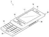
도 1에 도시된 바와 같이, 일반적인 슬라이드형 휴대 단말기(1)는, 전면에 디스플레이부(11)를 포함하는 상부 케이스(10)와 키 입력부(21)를 포함하는 하부 케이스(20)로 구성될 수 있다. 상부 케이스(10)는 하부 케이스(20) 위에서 슬라이딩하여 상하로 이동할 수 있다.As shown in FIG. 1, a typical slide-type
디스플레이부(11)는 사용자에게 원하는 화면을 출력하거나 사용자로부터 명령을 입력 받는 사용자 인터페이스(User Interface)의 역할을 할 수 있다. 이러한 디스플레이부(11)로는 LCD(Liquid Crystal Display), OLED(Organic Light Emitting Diodes) 등을 사용할 수 있다.The
하부 케이스(20)의 상부면에는 사용자로부터 조작 명령을 입력 받는 키 입력부(21)가 형성될 수 있으며, 상부 케이스(10)가 슬라이딩하여 이동하여 하부 케이스(20)로부터 멀어지면 외부로 노출될 수 있다. 이러한 키 입력부(21)는 키 패 드(Key pad)나 키 버튼(Key button)의 형태로 구현될 수 있다.The upper surface of the
한편, 도 1에서는 상부 케이스(10)의 하단부, 즉, 디스플레이부(11)의 하단부에 사용자로부터 조작 명령을 입력 받는 보조 키 입력부(12)가 형성된 예를 도시하고 있으나, 상부 케이스(10)의 상부면 전체가 디스플레이부(11)로 이루어질 수도 있다. 이러한 보조 키 입력부(12)는 상부 케이스(10)의 하단부 또는 측면에 형성될 수 있으며, 상부 케이스(10)와 하부 케이스(20)가 결합한 경우 사용자로부터 입력을 받기 위해 휴대 단말기(1) 전원의 온/오프(On/Off)를 위한 전원 키, 상대방과의 통화를 위한 통화 키, 디스플레이부(11) 상에 표시된 메뉴들을 선택하기 위한 방향 키 등과 같은 최소한의 기능 키들로 이루어질 수 있다.Meanwhile, FIG. 1 illustrates an example in which an auxiliary
도 1에 도시된 바와 같이, 휴대 단말기(1)는 상부 케이스(10)의 상단부에 마련되어 음성 신호를 출력하는 수화부(13)와, 하부 케이스(20)의 하단부에 마련되어 음성 신호를 입력하는 송화부(22)를 구비할 수 있다. 사용자는 수화부(13)를 귀에 대고 상대방으로부터 수신되는 음성 신호를 들을 수 있고, 송화부(22)에 입을 대고 말하여 상대방에게 음성 신호를 전달할 수 있다. 또한, 휴대 단말기(1)는 상부 케이스(10)의 상단부에 전방의 피사체를 촬영하거나 영상 통화를 하기 위한 카메라부(14)를 구비할 수 있다.As shown in FIG. 1, the
한편, 상부 케이스(10)와 하부 케이스(20) 사이에는 상부 케이스(10)가 하부 케이스(20) 위에서 슬라이딩하여 이동할 수 있도록 안내하는 슬라이딩 힌지(30)를 포함할 수 있다. 도 2에 도시된 바와 같이, 슬라이딩 힌지(30)는 상부 케이스(10)의 하부면에 연결되는 제1 슬라이딩 부재(31), 하부 케이스(20)의 상부면에 연결되 는 제2 슬라이딩 부재(32) 및 제1 슬라이딩 부재(31)와 제2 슬라이딩 부재(32) 사이에 설치되는 힌지부(33)를 포함하여 구성될 수 있다. 상부 케이스(10)의 슬라이딩 이동을 안내하기 위해 제1 슬라이딩 부재(31)의 양 측면에는 상부 케이스(10)의 이동 방향을 따라 길게 형성된 돌기가 구비되고, 제2 슬라이딩 부재(32)의 양 측면에는 제1 슬라이딩 부재의 돌기(31a)가 삽입될 수 있도록 길게 형성된 홈(32b)이 구비될 수 있다. 힌지부(33)는 상부 케이스(10)가 그 위치에 따라 자동 또는 반자동으로 슬라이딩하여 이동할 수 있도록 탄성력을 제공하는 압축 스프링과 같은 탄성 부재를 구비할 수 있다. 도 2에 도시된 슬라이딩 힌지(30)의 구조는 예시적인 것으로, 이에 국한되지 않으며, 당업자에 의해 얼마든지 변경 가능하다.On the other hand, between the
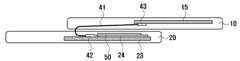
한편, 도 3에 도시된 바와 같이, 하부 케이스(20)의 내부에는 제1 전자 회로 기판(23)이, 상부 케이스(10)의 내부에는 제2 전자 회로 기판(15)이 장착될 수 있다. 상부 케이스(10)에 구비된 디스플레이부(11), 카메라부(14)와 같은 다양한 기능 모듈들은 상부 케이스(10) 내에 장착된 제2 전자 회로 기판(15)에 전기적으로 연결되며, 하부 케이스(20) 내에 장착된 제1 전자 회로 기판(23)으로부터 전기적 신호를 받아 제어될 수 있다. 제1 전자 회로 기판(23) 및 제2 전자 회로 기판(15)은 대략 얇은 플레이트 형상을 가지고, 상부면에 각종 전자 부품들과 이들을 연결하는 배선들을 포함할 수 있다. 전자 부품은 모뎀 칩(Modem Chip)과 같은 다양한 종류의 소자를 의미할 수 있다. 바람직하게는, 제1 전자 회로 기판(23) 및 제2 전자 회로 기판(15)은 인쇄 회로 기판(Printed Circuit Board, PCB)을 사용할 수 있다.As illustrated in FIG. 3, the first
한편, 휴대 단말기(1)를 사용할 때에 하부 케이스(20)의 제1 전자 회로 기판(23)에 장착된 각종 전자 부품들로부터 노이즈가 발생할 수 있다. 여기서, 노이즈는 디스플레이부(11) 또는 카메라부(14)로부터 데이터가 전달될 때에 발생하는 노이즈, 전원에 의한 노이즈, 안테나부(도시되지 않음)로부터 방사되어 상부 케이스로 커플링(Coupling)되어 방사되는 노이즈 등을 의미할 수 있다. 따라서, 제1 전자 회로 기판(23)의 상부면에 이러한 노이즈를 차폐하는 노이즈 차단부(24)를 설치할 수 있다. 바람직하게는, 노이즈 차단부(24)로서 도 2에 도시된 바와 같은 쉴드 캔(Shield can)을 사용할 수 있다. 쉴드 캔의 표면에는 EMI(Electromagnetic Interference) 도료가 도포될 수 있다. 노이즈 차단부(24)은 전자 부품들로부터 일정 간격 이격되어 설치될 수 있으며, 그 형상은 제1 전자 회로 기판(23)에 장착된 전자 부품들의 종류, 배치 구조 등에 따라 결정될 수 있다.Meanwhile, when the
상술한 바와 같이, 제2 전자 회로 기판(15)에 연결된 디스플레이부(11), 카메라부(14)와 같은 다양한 기능 모듈들은 제1 전자 회로 기판(23)으로부터 전기적 신호를 받아 제어될 수 있는데, 제1 전자 회로 기판(23)과 제2 전자 회로 기판(15)을 연결하여 각종 전기적 신호를 송수신하기 위해 연성 인쇄 회로 기판(Flexible Printed Circuit Board, 이하 FPCB라고 칭함)(40)을 이용할 수 있다. 일반적으로, FPCB(40)는 유연한 플라스틱 재질의 박판 필름에 미세 회로가 인쇄된 유동 가능한 인쇄 회로를 의미한다.As described above, various functional modules such as the
본 발명의 일 실시예에 따른 연성 인쇄 회로 기판을 구비하는 휴대 단말기(1)의 경우, 제1 전자 회로 기판(23)과 연결되는 FPCB(40)의 일단에 연결되고, 내부에 FPCB(40)의 그라운드 라인과 연결되는 그라운드 층이 형성되며, 제1 전자 회로 기판(23) 상에 장착된 전자 부품들로부터 발생하는 노이즈를 차폐하는 노이즈 차단부(24)와 연결되는 그라운드 확장부(50)를 포함할 수 있다.In the case of the
도 4는 본 발명의 일 실시예에 따른 연성 인쇄 회로 기판을 구비하는 휴대 단말기에서 연성 인쇄 회로 기판과 연결된 그라운드 확장부의 구조를 나타내는 도면이다.4 is a diagram illustrating a structure of a ground extension connected to a flexible printed circuit board in a mobile terminal having a flexible printed circuit board according to an exemplary embodiment of the present invention.
도 4에 도시된 바와 같이, FPCB(40)는 복수의 층(Layer)으로 이루어지고 내부에 복수의 데이터 라인, 전원 라인 및 그라운드 라인(도시되지 않음)을 구비하는 FPCB 연결부(41)와, FPCB 연결부(41)의 양 끝단에 형성되어 제1 전자 회로 기판(23) 및 제2 전자 회로 기판(15)과 연결하기 위한 제1 커넥터(42) 및 제2 커넥터(43)를 포함하여 구성될 수 있다. 즉, FPCB 연결부(41)는 제1 전자 회로 기판(23)과 제2 전자 회로 기판(15)을 연결하여 전원, 각종 제어 신호 및 데이터 신호를 송수신하는 통신 경로의 역할을 할 수 있다. FPCB 연결부(41)의 그라운드 라인의 양 끝단은 각각 제1 전자 회로 기판(23)의 그라운드와 제2 전자 회로 기판(15)의 그라운드와 연결될 수 있다. FPCB 연결부(41)의 데이터 라인, 전원 라인 및 그라운드 라인은 구리 도체로 이루어질 수 있다. 한편, 도시되지는 않았으나, 제1 커넥터(42) 및 제2 커넥터(43)는 각각 복수의 단자를 포함하는 헤더(Header)와 소켓(Socket)으로 이루어질 수 있다. 제1 커넥터(42) 및 제2 커넥터(43)의 그라운드 면에는 제1 전자 회로 기판(23) 및 제2 전자 회로 기판(15)에 결합할 때에 정전기 등에 의한 영향을 최소화하기 위해 EMI 도료가 도포될 수 있다. FPCB(40)는 그 사용 조건에 따라 다양하게 구현될 수 있으며 그 단면 구조에 대해서는 잘 알려져 있으므로, 여기서 자세한 설명은 생략한다.As shown in FIG. 4, the
도 4에 도시된 바와 같이, 그라운드 확장부(50)는 제1 전자 회로 기판(23)과 연결되는 FPCB(40)의 일단에 연결되고, 내부에 FPCB(40)의 그라운드 라인과 연결되는 그라운드 층(도 6의 54a)이 형성될 수 있으며, FPCB(40)의 일단으로부터 길이 방향을 따라 제1 확장부(51), 제2 확장부(52) 및 제3 확장부(53)로 구성될 수 있다.As shown in FIG. 4, the
제1 확장부(51)는 FPCB(40)와 제1 전자 회로 기판(23)을 연결하는 제1 커넥터(42)에 연결될 수 있다. 제3 확장부(53)는 FPCB(40)의 그라운드를 확장하기 위해 노이즈 차단부(24)에 접지될 수 있다. 제2 확장부(52)는 제1 확장부(51)와 제3 확장부(53) 사이에서 이들을 연결할 수 있다. 제3 확장부(53)는 노이즈 차단부(24)에 접지될 수 있도록 경질의 재질을 가질 수 있으며, 그라운드 확장부(50)를 연결할 때에 경질의 제3 확장부(53)으로 인해 꺾임 등에 의한 손상을 방지하기 위해 제1 확장부(51) 및 제2 확장부(52)는 플렉셔블(Flexible)한 연성의 재질을 가질 수 있다. 제1 확장부(51) 내지 제3 확장부(53)의 단면 구조는 내부에 그라운드 층(도 6의 54a)을 가진다는 점에서 같으나, 그 표면 처리에 있어서 차이점을 가지고 있다. 이에 대해서는 도 6을 참조하여 자세히 후술하기로 한다.The
한편, 도 4에 도시된 그라운드 확장부(50)의 구조는 형태는 예시적인 것으로서, 그라운드 확장부(50)의 구조는 접지를 위한 노이즈 차단부의 형상, 접지 위치 등의 조건에 따라 얼마든지 변경 가능하다.Meanwhile, the structure of the
도 5는 본 발명의 일 실시예에 따른 연성 인쇄 회로 기판을 구비하는 휴대 단말기에서 연성 인쇄 회로 기판과 연결된 그라운드 확장부가 제1 전자 회로 기판의 노이즈 차단부에 연결된 모습을 나타내는 도면이다.FIG. 5 is a diagram illustrating a ground extension part connected to a flexible printed circuit board connected to a noise blocking part of a first electronic circuit board in a mobile terminal having a flexible printed circuit board according to an exemplary embodiment of the present disclosure.
도 5에 도시된 바와 같이, FPCB(40)의 일단은 제1 커넥터(42)를 통해 제1 전자 회로 기판(23)에 전기적으로 연결될 수 있으며, FPCB(40)의 타단은 제2 커넥터(43)를 통해 제2 전자 회로 기판(15)에 전기적으로 연결될 수 있다. 그라운드 확장부(50)는 제1 확장부(51)를 통해 제1 커넥터(42)에 연결되고, 제3 확장부(53)를 통해 노이즈 차단부(24)인 노이즈 차단부(24)에 접지될 수 있다. 따라서, FPCB(40)를 통해 전달되는 노이즈 및 ESD 서지를 그라운드 확장부(50)를 통해 노이즈 차단부(24)로 우회시켜 그라운드를 확장할 수 있다.As shown in FIG. 5, one end of the
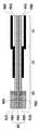
도 6은 본 발명의 일 실시예에 따른 연성 인쇄 회로 기판을 구비하는 휴대 단말기에서 연성 인쇄 회로 기판과 연결된 그라운드 확장부의 단면 구조를 나타내는 도면이다.6 is a diagram illustrating a cross-sectional structure of a ground extension connected to a flexible printed circuit board in a mobile terminal having a flexible printed circuit board according to an exemplary embodiment of the present invention.
도 6에 도시된 바와 같이, 제1 확장부(51), 제2 확장부(52) 및 제3 확장부(53)로 이루어진 그라운드 확장부(50)는 그 내부에 그라운드 층(54a)이 형성될 수 있다. 이러한 그라운드 층(54a)은 구리(Copper)로 이루어진 동박 층으로 이루어질 수 있다. 그라운드 층(54a)의 상부면과 하부면에는 보호 필름 층(Cover Lay) 또는 PI(Polyimide) 필름 층(54b, 54c)이 형성될 수 있다.As shown in FIG. 6, the
도 6에 도시된 바와 같이, 제1 확장부(51)의 상부면 또는 하부면에는 나노(Nano) 코팅 층(55a, 55b)을 형성할 수 있다. 이러한 나노 코팅 층(55a, 55b)은 도전성이 우수한 금(Au), 은(Ag) 등의 나노 입자를 분사하여 얇은 막 형태로 형성함으로써 얻을 수 있다. 나노 코팅 층(55a, 55b)은 뛰어난 정전기 방전 차폐 기능을 가지고 있으므로, 제1 확장부(51)와 연결된 제1 커넥터(42)에서 정전기 방전 현상이 발생하여 제1 전자 회로 기판(23)에 장착된 각종 전자 부품들을 손상시키는 것을 방지할 수 있다. 여기서는 나노 코팅 층을 형성한 예를 들고 있으나, 도전성이 우수한 물질이라면 어떠한 재질로 코팅 층을 형성하여도 무방하다.As illustrated in FIG. 6,
또한, 제1 확장부(51)의 상부면 또는 하부면, 또는 제2 확장부(52)의 상부면 또는 하부면에는 FPCB(40)가 연결되는 제1 커넥터(42)와 마찬가지로, 정전기 등에 의한 영향을 최소화하고 그라운드를 확보하기 위해 EMI 도료(56a, 56b)가 도포될 수 있다.In addition, similar to the
한편, 도 6에 도시된 바와 같이, 제3 확장부(53)의 상부면 또는 하부면 중, 노이즈 차단부(24)와 접지되는 부분은 제3 확장부(53)와 노이즈 차단부(24)의 접지를 위해 동박 코팅 층(57a, 57b)이 형성될 수 있다. 도시되지는 않았으나, 제3 확장부(53)의 상부면 또는 하부면에 금 도금 층(Gold coating), 구리 도금 층(Copper, Cu Plating) 등을 형성하여 동박 코팅 층(57a, 57b)을 형성할 수 있다. 제3 확장부(53)의 상부면 또는 하부면 중에서 동박 코팅 층(57a, 57b)이 형성되는 부분은 노이즈 차단부(24)와 접지되는 부분으로서, 제3 확장부(53)의 상부면 또는 하부면 중 일부에 동박 코팅 층이 형성될 수도 있고, 제3 확장부(53)의 상부면 또는 하부면 전체에 동박 코팅 층이 형성될 수도 있다. 한편, 동박 코딩 층(57a, 57b)은 층간 접착제(도시되지 않음)를 이용하여 그라운드 층(54a)의 상부면과 하부 면에 형성된 보호 필름 층 또는 PI 필름 층에 접착될 수 있다.On the other hand, as shown in Figure 6, of the upper or lower surface of the
도 6에 도시된 바와 같이, 동박 코팅 층(57a, 57b)은 내부에 금속 충전물이 형성된 복수의 비아 홀(Via hole)(58a, 58b)을 통해 그라운드 층(54a)과 연결될 수 있다. 복수의 비아 홀(58a, 58b)은 제3 확장부(53) 내부의 그라운드 층(54a)과 제3 확장부(53)의 상부면 또는 하부면에 형성된 동박 코팅 층(57a, 57b)을 관통하여 형성될 수 있으며, 금속 충전물을 통해 그라운드 층(54a)과 동박 코팅 층(57a, 57b)이 전기적으로 연결될 수 있다. 따라서, 따라서, FPCB(40)를 통해 전달되는 노이즈 및 ESD 서지를 동박 코팅 층(57a, 57b)을 통해 노이즈 차단부(24)로 우회시킬 수 있다.As illustrated in FIG. 6, the copper
이상, 도 6에 도시된 그라운드 확장부의 단면 구조는 예시적인 것으로서, 이에 국한되지 않으며 당업자에 의해 얼마든지 변경 가능하다. 예를 들어, 도 6에서는 제1 확장부(51)의 상부면 및 하부면과 제2 확장부(52)의 상부면 및 하부면에 EMI 도료(56a, 56b)가 도포된 예를 도시하고 있으나, EMI 도료는 제1 확장부(51)의 상부면 또는 하부면에만 도포될 수도 있고, EMI 도료의 도포를 생략할 수도 있다.As described above, the cross-sectional structure of the ground extension shown in FIG. 6 is exemplary, and is not limited thereto and may be changed by those skilled in the art. For example, FIG. 6 illustrates an example in which EMI paints 56a and 56b are applied to the top and bottom surfaces of the
이상 설명한 바와 같이, 본 발명에서는 슬라이드형(Slide Type) 휴대 단말기(1)를 예로 들어 설명하고 있으나, 휴대 단말기의 형태는 이에 한정되지 않는다. 즉, 본 발명은 슬라이드형(Slide Type) 휴대 단말기, 폴더형(Folder type) 휴대 단말기, 회전형(Rotating type) 휴대 단말기, 또는 이들의 조합형(Combination type) 등 제1 전자 회로 기판과 제2 전자 회로 기판을 연결하기 위해 FPCB를 이용하는 다양한 형태의 휴대 단말기에도 적용할 수 있다.As described above, in the present invention, the slide type
상술한 바와 같이, 본 발명의 일 실시예에 따른 연성 인쇄 회로 기판을 구비하는 휴대 단말기에 따르면, 전자 회로 기판에 연결되는 연성 인쇄 회로 기판의 일단으로부터 연장된 그라운드 확장부를 전자 회로 기판 상에 설치된 노이즈 차단부에 연결함으로써, 그라운드를 확장할 수 있고 노이즈 및 정전기가 전자 회로 기판 상에 장착된 전자 부품들에 미치는 영향을 최소화할 수 있다. 또한, 간단한 구조로 휴대 단말기의 방사 성능 및 ESD 성능을 향상시킬 수 있다. 또한, 간단한 구조로 그라운드를 확장할 수 있으므로 휴대 단말기의 제조 비용을 절감할 수 있다.As described above, according to the mobile terminal having the flexible printed circuit board according to an embodiment of the present invention, the noise provided on the electronic circuit board, the ground extension extending from one end of the flexible printed circuit board connected to the electronic circuit board. By connecting to the breaker, the ground can be extended and the influence of noise and static electricity on the electronic components mounted on the electronic circuit board can be minimized. In addition, it is possible to improve the radiation performance and ESD performance of the portable terminal with a simple structure. In addition, since the ground can be expanded with a simple structure, the manufacturing cost of the portable terminal can be reduced.
한편, 본 명세서와 도면에는 본 발명의 바람직한 실시예에 대하여 개시하였으며, 비록 특정 용어들이 사용되었으나, 이는 단지 본 발명의 기술 내용을 쉽게 설명하고 발명의 이해를 돕기 위한 일반적인 의미에서 사용된 것이지, 본 발명의 범위를 한정하고자 하는 것은 아니다. 여기에 개시된 실시예 외에도 본 발명의 기술적 사상에 바탕을 둔 다른 변형예들이 실시 가능하다는 것은 본 발명이 속하는 기술 분야에서 통상의 지식을 가진 자에게 자명한 것이다.On the other hand, in the present specification and drawings have been described with respect to preferred embodiments of the present invention, although specific terms are used, it is merely used in a general sense to easily explain the technical details of the present invention and to help the understanding of the invention, It is not intended to limit the scope of the invention. It is to be understood by those skilled in the art that other modifications based on the technical idea of the present invention are possible in addition to the embodiments disclosed herein.
도 1은 본 발명의 일 실시예에 따른 연성 인쇄 회로 기판을 구비하는 휴대 단말기를 나타내는 사시도이다.1 is a perspective view illustrating a mobile terminal having a flexible printed circuit board according to an embodiment of the present invention.
도 2는 본 발명의 일 실시예에 따른 연성 인쇄 회로 기판을 구비하는 휴대 단말기의 구성을 나타내는 분해 사시도이다.2 is an exploded perspective view illustrating a configuration of a mobile terminal having a flexible printed circuit board according to an embodiment of the present invention.
도 3a 및 도 3b는 본 발명의 일 실시예에 따른 연성 인쇄 회로 기판을 구비하는 휴대 단말기의 구성을 나타내는 측면도이다.3A and 3B are side views illustrating a configuration of a portable terminal having a flexible printed circuit board according to an embodiment of the present invention.
도 4는 본 발명의 일 실시예에 따른 연성 인쇄 회로 기판을 구비하는 휴대 단말기에서 연성 인쇄 회로 기판과 연결된 그라운드 확장부의 구조를 나타내는 도면이다.4 is a diagram illustrating a structure of a ground extension connected to a flexible printed circuit board in a mobile terminal having a flexible printed circuit board according to an exemplary embodiment of the present invention.
도 5는 본 발명의 일 실시예에 따른 연성 인쇄 회로 기판을 구비하는 휴대 단말기에서 연성 인쇄 회로 기판과 연결된 그라운드 확장부가 제1 전자 회로 기판의 노이즈 차단부에 연결된 모습을 나타내는 도면이다.FIG. 5 is a diagram illustrating a ground extension part connected to a flexible printed circuit board connected to a noise blocking part of a first electronic circuit board in a mobile terminal having a flexible printed circuit board according to an exemplary embodiment of the present disclosure.
도 6은 본 발명의 일 실시예에 따른 연성 인쇄 회로 기판을 구비하는 휴대 단말기에서 연성 인쇄 회로 기판과 연결된 그라운드 확장부의 단면 구조를 나타내는 도면이다.6 is a diagram illustrating a cross-sectional structure of a ground extension connected to a flexible printed circuit board in a mobile terminal having a flexible printed circuit board according to an exemplary embodiment of the present invention.
<도면의 주요 부분에 대한 부호의 설명><Explanation of symbols for the main parts of the drawings>
1: 휴대 단말기10: 상부 케이스1: mobile terminal 10: upper case
11: 디스플레이부12: 보조 키 입력부11: display unit 12: auxiliary key input unit
13: 수화부14: 카메라부13: receiver 14: camera
15: 제2 전자 회로 기판15: second electronic circuit board
20: 하부 케이스21: 키 입력부20: lower case 21: key input unit
22: 송화부23: 제1 전자 회로 기판22: transmitter section 23: first electronic circuit board
24: 노이즈 차단부24: noise blocking unit
30: 슬라이딩 힌지31: 제1 슬라이딩 부재30: sliding hinge 31: first sliding member
32: 제2 슬라이딩 부재33: 힌지부32: second sliding member 33: hinge portion
40: FPCB41: FPCB 연결부40: FPCB 41: FPCB connection
42: 제1 커넥터43: 제2 커넥터42: first connector 43: second connector
50: 그라운드 확장부51: 제1 확장부50: ground extension portion 51: first expansion portion
52: 제2 확장부53: 제3 확장부52: second extension part 53: third extension part
Claims (7)
Translated fromKoreanPriority Applications (4)
| Application Number | Priority Date | Filing Date | Title |
|---|---|---|---|
| KR1020090034963AKR20100116321A (en) | 2009-04-22 | 2009-04-22 | Mobile device having flexible printed circuit board |
| EP10158477AEP2244444A1 (en) | 2009-04-22 | 2010-03-30 | Mobile terminal having flexible printed circuit board |
| US12/755,604US8532696B2 (en) | 2009-04-22 | 2010-04-07 | Mobile terminal having flexible printed circuit board |
| CN201010167918ACN101873362A (en) | 2009-04-22 | 2010-04-22 | Mobile terminal with flexible printed circuit board |
Applications Claiming Priority (1)
| Application Number | Priority Date | Filing Date | Title |
|---|---|---|---|
| KR1020090034963AKR20100116321A (en) | 2009-04-22 | 2009-04-22 | Mobile device having flexible printed circuit board |
Publications (1)
| Publication Number | Publication Date |
|---|---|
| KR20100116321Atrue KR20100116321A (en) | 2010-11-01 |
Family
ID=42664869
Family Applications (1)
| Application Number | Title | Priority Date | Filing Date |
|---|---|---|---|
| KR1020090034963ACeasedKR20100116321A (en) | 2009-04-22 | 2009-04-22 | Mobile device having flexible printed circuit board |
Country Status (4)
| Country | Link |
|---|---|
| US (1) | US8532696B2 (en) |
| EP (1) | EP2244444A1 (en) |
| KR (1) | KR20100116321A (en) |
| CN (1) | CN101873362A (en) |
Cited By (3)
| Publication number | Priority date | Publication date | Assignee | Title |
|---|---|---|---|---|
| WO2017122907A1 (en)* | 2016-01-12 | 2017-07-20 | 삼성전자 주식회사 | Rf cable connection device and electronic device having same |
| WO2022215947A1 (en)* | 2021-04-05 | 2022-10-13 | 삼성전자 주식회사 | Display module accounting for esd phenomenon, and electronic device comprising display module |
| US11675392B2 (en) | 2020-12-01 | 2023-06-13 | Samsung Electronics Co., Ltd. | Electronic device including rollable display |
Families Citing this family (15)
| Publication number | Priority date | Publication date | Assignee | Title |
|---|---|---|---|---|
| KR20100112390A (en)* | 2009-04-09 | 2010-10-19 | 삼성전자주식회사 | Mobile device having shielding structure preventing noise for electronic circuit board |
| KR101789539B1 (en) | 2011-02-24 | 2017-10-26 | 엘지전자 주식회사 | Mobile terminal |
| JP5858641B2 (en)* | 2011-05-10 | 2016-02-10 | キヤノン株式会社 | Information processing apparatus, system including information processing apparatus and external apparatus, system control method, and program |
| JP5062705B1 (en)* | 2011-07-07 | 2012-10-31 | Necインフロンティア株式会社 | Flexible printed cable and information processing apparatus |
| KR20130026891A (en)* | 2011-09-06 | 2013-03-14 | 엘지전자 주식회사 | Mobile terminal and power management unit thereof |
| JP5753501B2 (en)* | 2012-02-10 | 2015-07-22 | ホシデン株式会社 | Component module |
| DE102012212025A1 (en)* | 2012-07-10 | 2014-01-16 | Osram Gmbh | LIGHT MODULE |
| TW201426468A (en)* | 2012-12-17 | 2014-07-01 | Hon Hai Prec Ind Co Ltd | Electronic device having capacitive touch screen |
| US10852025B2 (en)* | 2013-04-30 | 2020-12-01 | Ademco Inc. | HVAC controller with fixed segment display having fixed segment icons and animation |
| TWI577252B (en)* | 2015-10-06 | 2017-04-01 | 挺暉工業股份有限公司 | A flexible printed circuit board, a connector assembly and an electronic device |
| KR102551188B1 (en) | 2018-06-26 | 2023-07-04 | 엘지이노텍 주식회사 | A lens moving unit, and camera module and optical instrument including the same |
| US11886240B2 (en) | 2018-07-17 | 2024-01-30 | Huawei Technologies Co., Ltd. | Mobile terminal with a bendable structure |
| JP7483354B2 (en)* | 2019-11-27 | 2024-05-15 | キヤノン株式会社 | Imaging device |
| CN113412039A (en)* | 2020-03-17 | 2021-09-17 | 中兴通讯股份有限公司 | Electronic device and method for manufacturing electronic device |
| EP4328707A4 (en) | 2021-11-29 | 2024-08-07 | Samsung Electronics Co., Ltd. | FLEXIBLE CIRCUIT BOARD CONNECTION ARRANGEMENT AND ELECTRONIC DEVICE THEREOF |
Family Cites Families (20)
| Publication number | Priority date | Publication date | Assignee | Title |
|---|---|---|---|---|
| US6980092B2 (en)* | 2000-04-06 | 2005-12-27 | Gentex Corporation | Vehicle rearview mirror assembly incorporating a communication system |
| US6879849B2 (en)* | 2002-02-21 | 2005-04-12 | Telefonaktiebolaget L M Ericsson (Publ) | In-built antenna for mobile communication device |
| KR100617690B1 (en)* | 2003-11-10 | 2006-08-28 | 삼성전자주식회사 | Sliding type portable wireless terminal |
| GB2414115B (en)* | 2004-05-14 | 2006-04-19 | Antenova Ltd | An improved mobile telephone handset |
| KR100640795B1 (en)* | 2005-03-28 | 2006-11-06 | 엘지전자 주식회사 | Camera coupling structure of mobile communication terminal |
| TWI260193B (en)* | 2005-04-15 | 2006-08-11 | Benq Corp | Mobile device |
| CN101433062B (en)* | 2006-03-02 | 2011-11-09 | 松下电器产业株式会社 | Portable terminal |
| KR101162215B1 (en)* | 2006-08-22 | 2012-07-04 | 엘지전자 주식회사 | Mobile phone |
| US8032186B2 (en)* | 2006-10-17 | 2011-10-04 | Lg Electronics Inc. | Mobile communication terminal and method of connecting call thereof |
| KR100911007B1 (en)* | 2007-05-18 | 2009-08-05 | 삼성에스디아이 주식회사 | Chassis base assembly and display device including the same |
| TW200915822A (en)* | 2007-09-29 | 2009-04-01 | Asustek Comp Inc | Handheld electronic apparatus |
| TWI337518B (en)* | 2007-11-07 | 2011-02-11 | Htc Corp | Electronic device |
| KR101495157B1 (en)* | 2007-11-27 | 2015-02-24 | 엘지전자 주식회사 | Mobile terminal |
| JP2009212966A (en)* | 2008-03-05 | 2009-09-17 | Nec Corp | Mobile electronic apparatus with metallic decorative panel |
| KR101529913B1 (en)* | 2008-03-25 | 2015-06-18 | 엘지전자 주식회사 | Slide module and portable terminal having the same |
| JP4892514B2 (en)* | 2008-04-22 | 2012-03-07 | 日本オプネクスト株式会社 | Optical communication module and flexible printed circuit board |
| KR100989478B1 (en)* | 2008-05-15 | 2010-10-22 | 엘에스전선 주식회사 | Micro coaxial cable assembly and slide mobile phone with same |
| DE112009002020T5 (en)* | 2008-08-21 | 2011-06-30 | Intersil Americas Inc., Calif. | Noise reduction for an antenna module |
| KR101534505B1 (en)* | 2008-11-28 | 2015-07-09 | 엘지전자 주식회사 | Mobile terminal |
| KR101670258B1 (en)* | 2009-07-06 | 2016-10-31 | 삼성전자 주식회사 | Mobile device having flexible printed circuit board |
- 2009
- 2009-04-22KRKR1020090034963Apatent/KR20100116321A/ennot_activeCeased
- 2010
- 2010-03-30EPEP10158477Apatent/EP2244444A1/ennot_activeWithdrawn
- 2010-04-07USUS12/755,604patent/US8532696B2/ennot_activeExpired - Fee Related
- 2010-04-22CNCN201010167918Apatent/CN101873362A/enactivePending
Cited By (4)
| Publication number | Priority date | Publication date | Assignee | Title |
|---|---|---|---|---|
| WO2017122907A1 (en)* | 2016-01-12 | 2017-07-20 | 삼성전자 주식회사 | Rf cable connection device and electronic device having same |
| US10616995B2 (en) | 2016-01-12 | 2020-04-07 | Samsung Electronics Co., Ltd. | RF cable connection device and electronic device having same |
| US11675392B2 (en) | 2020-12-01 | 2023-06-13 | Samsung Electronics Co., Ltd. | Electronic device including rollable display |
| WO2022215947A1 (en)* | 2021-04-05 | 2022-10-13 | 삼성전자 주식회사 | Display module accounting for esd phenomenon, and electronic device comprising display module |
Also Published As
| Publication number | Publication date |
|---|---|
| US20100273539A1 (en) | 2010-10-28 |
| US8532696B2 (en) | 2013-09-10 |
| EP2244444A1 (en) | 2010-10-27 |
| CN101873362A (en) | 2010-10-27 |
Similar Documents
| Publication | Publication Date | Title |
|---|---|---|
| KR20100116321A (en) | Mobile device having flexible printed circuit board | |
| KR101670258B1 (en) | Mobile device having flexible printed circuit board | |
| US8073514B2 (en) | Electronic device having a dual autodiplexing antenna | |
| JP5345653B2 (en) | PCB antenna | |
| KR101561945B1 (en) | Antenna device and portable terminal having the same | |
| US8060162B2 (en) | Slider grounding to mitigate unwanted coupling and lossy antenna resonance | |
| TW202107769A (en) | Antenna structure and wireless communication device using the same | |
| KR101261983B1 (en) | Mobile terminal having FPCB cable | |
| CN113013617A (en) | Antenna assembly and electronic equipment | |
| US8345448B2 (en) | Mobile terminal having noise shielding structure for electronic circuit board | |
| JP2009188714A (en) | Mobile phone equipment | |
| KR100700575B1 (en) | Multilayer Circuit Board of Mobile Communication Terminal | |
| KR20100026780A (en) | Antenna apparatus for printed circuits board having sub antenna | |
| TW200537736A (en) | Multi-frequency hidden antenna device | |
| JP2007013014A (en) | Folding pocket electronic instrument and flexible wiring substrate | |
| KR101104948B1 (en) | Slide device on mobile device | |
| KR100696008B1 (en) | Dual clamshell mobile communication terminal with built-in antenna | |
| KR100757319B1 (en) | Dual Board Bonded Broadband Antenna | |
| KR20100062058A (en) | Electronic circuit board connector and mobile device having the same | |
| CN1901277A (en) | Antenna device for portable terminal, portable terminal, and method for providing antenna in portable terminal | |
| JP2012043900A (en) | Shield structure of electronic component and electronic equipment using the same |
Legal Events
| Date | Code | Title | Description |
|---|---|---|---|
| PA0109 | Patent application | Patent event code:PA01091R01D Comment text:Patent Application Patent event date:20090422 | |
| PG1501 | Laying open of application | ||
| A201 | Request for examination | ||
| PA0201 | Request for examination | Patent event code:PA02012R01D Patent event date:20140324 Comment text:Request for Examination of Application Patent event code:PA02011R01I Patent event date:20090422 Comment text:Patent Application | |
| E902 | Notification of reason for refusal | ||
| PE0902 | Notice of grounds for rejection | Comment text:Notification of reason for refusal Patent event date:20150313 Patent event code:PE09021S01D | |
| E601 | Decision to refuse application | ||
| PE0601 | Decision on rejection of patent | Patent event date:20150622 Comment text:Decision to Refuse Application Patent event code:PE06012S01D Patent event date:20150313 Comment text:Notification of reason for refusal Patent event code:PE06011S01I |