KR20100109389A - Multilayer wiring substrate, stack structure sensor package, and method of manufacturing stack structure sensor package - Google Patents
Multilayer wiring substrate, stack structure sensor package, and method of manufacturing stack structure sensor packageDownload PDFInfo
- Publication number
- KR20100109389A KR20100109389AKR1020100024181AKR20100024181AKR20100109389AKR 20100109389 AKR20100109389 AKR 20100109389AKR 1020100024181 AKR1020100024181 AKR 1020100024181AKR 20100024181 AKR20100024181 AKR 20100024181AKR 20100109389 AKR20100109389 AKR 20100109389A
- Authority
- KR
- South Korea
- Prior art keywords
- multilayer wiring
- wiring board
- edge portion
- hole
- connection terminal
- Prior art date
- Legal status (The legal status is an assumption and is not a legal conclusion. Google has not performed a legal analysis and makes no representation as to the accuracy of the status listed.)
- Ceased
Links
Images


Classifications
- H—ELECTRICITY
- H10—SEMICONDUCTOR DEVICES; ELECTRIC SOLID-STATE DEVICES NOT OTHERWISE PROVIDED FOR
- H10F—INORGANIC SEMICONDUCTOR DEVICES SENSITIVE TO INFRARED RADIATION, LIGHT, ELECTROMAGNETIC RADIATION OF SHORTER WAVELENGTH OR CORPUSCULAR RADIATION
- H10F39/00—Integrated devices, or assemblies of multiple devices, comprising at least one element covered by group H10F30/00, e.g. radiation detectors comprising photodiode arrays
- H10F39/80—Constructional details of image sensors
- H10F39/804—Containers or encapsulations
- H—ELECTRICITY
- H05—ELECTRIC TECHNIQUES NOT OTHERWISE PROVIDED FOR
- H05K—PRINTED CIRCUITS; CASINGS OR CONSTRUCTIONAL DETAILS OF ELECTRIC APPARATUS; MANUFACTURE OF ASSEMBLAGES OF ELECTRICAL COMPONENTS
- H05K3/00—Apparatus or processes for manufacturing printed circuits
- H05K3/46—Manufacturing multilayer circuits
- H—ELECTRICITY
- H01—ELECTRIC ELEMENTS
- H01L—SEMICONDUCTOR DEVICES NOT COVERED BY CLASS H10
- H01L23/00—Details of semiconductor or other solid state devices
- H01L23/02—Containers; Seals
- H01L23/04—Containers; Seals characterised by the shape of the container or parts, e.g. caps, walls
- H01L23/053—Containers; Seals characterised by the shape of the container or parts, e.g. caps, walls the container being a hollow construction and having an insulating or insulated base as a mounting for the semiconductor body
- H—ELECTRICITY
- H01—ELECTRIC ELEMENTS
- H01L—SEMICONDUCTOR DEVICES NOT COVERED BY CLASS H10
- H01L23/00—Details of semiconductor or other solid state devices
- H01L23/12—Mountings, e.g. non-detachable insulating substrates
- H—ELECTRICITY
- H01—ELECTRIC ELEMENTS
- H01L—SEMICONDUCTOR DEVICES NOT COVERED BY CLASS H10
- H01L23/00—Details of semiconductor or other solid state devices
- H01L23/48—Arrangements for conducting electric current to or from the solid state body in operation, e.g. leads, terminal arrangements ; Selection of materials therefor
- H—ELECTRICITY
- H10—SEMICONDUCTOR DEVICES; ELECTRIC SOLID-STATE DEVICES NOT OTHERWISE PROVIDED FOR
- H10F—INORGANIC SEMICONDUCTOR DEVICES SENSITIVE TO INFRARED RADIATION, LIGHT, ELECTROMAGNETIC RADIATION OF SHORTER WAVELENGTH OR CORPUSCULAR RADIATION
- H10F39/00—Integrated devices, or assemblies of multiple devices, comprising at least one element covered by group H10F30/00, e.g. radiation detectors comprising photodiode arrays
- H10F39/011—Manufacture or treatment of image sensors covered by group H10F39/12
- H—ELECTRICITY
- H10—SEMICONDUCTOR DEVICES; ELECTRIC SOLID-STATE DEVICES NOT OTHERWISE PROVIDED FOR
- H10F—INORGANIC SEMICONDUCTOR DEVICES SENSITIVE TO INFRARED RADIATION, LIGHT, ELECTROMAGNETIC RADIATION OF SHORTER WAVELENGTH OR CORPUSCULAR RADIATION
- H10F77/00—Constructional details of devices covered by this subclass
- H10F77/50—Encapsulations or containers
- H—ELECTRICITY
- H10—SEMICONDUCTOR DEVICES; ELECTRIC SOLID-STATE DEVICES NOT OTHERWISE PROVIDED FOR
- H10F—INORGANIC SEMICONDUCTOR DEVICES SENSITIVE TO INFRARED RADIATION, LIGHT, ELECTROMAGNETIC RADIATION OF SHORTER WAVELENGTH OR CORPUSCULAR RADIATION
- H10F99/00—Subject matter not provided for in other groups of this subclass
- H—ELECTRICITY
- H01—ELECTRIC ELEMENTS
- H01L—SEMICONDUCTOR DEVICES NOT COVERED BY CLASS H10
- H01L2224/00—Indexing scheme for arrangements for connecting or disconnecting semiconductor or solid-state bodies and methods related thereto as covered by H01L24/00
- H01L2224/01—Means for bonding being attached to, or being formed on, the surface to be connected, e.g. chip-to-package, die-attach, "first-level" interconnects; Manufacturing methods related thereto
- H01L2224/02—Bonding areas; Manufacturing methods related thereto
- H01L2224/04—Structure, shape, material or disposition of the bonding areas prior to the connecting process
- H01L2224/04042—Bonding areas specifically adapted for wire connectors, e.g. wirebond pads
- H—ELECTRICITY
- H01—ELECTRIC ELEMENTS
- H01L—SEMICONDUCTOR DEVICES NOT COVERED BY CLASS H10
- H01L2224/00—Indexing scheme for arrangements for connecting or disconnecting semiconductor or solid-state bodies and methods related thereto as covered by H01L24/00
- H01L2224/01—Means for bonding being attached to, or being formed on, the surface to be connected, e.g. chip-to-package, die-attach, "first-level" interconnects; Manufacturing methods related thereto
- H01L2224/10—Bump connectors; Manufacturing methods related thereto
- H01L2224/15—Structure, shape, material or disposition of the bump connectors after the connecting process
- H01L2224/16—Structure, shape, material or disposition of the bump connectors after the connecting process of an individual bump connector
- H—ELECTRICITY
- H01—ELECTRIC ELEMENTS
- H01L—SEMICONDUCTOR DEVICES NOT COVERED BY CLASS H10
- H01L2224/00—Indexing scheme for arrangements for connecting or disconnecting semiconductor or solid-state bodies and methods related thereto as covered by H01L24/00
- H01L2224/01—Means for bonding being attached to, or being formed on, the surface to be connected, e.g. chip-to-package, die-attach, "first-level" interconnects; Manufacturing methods related thereto
- H01L2224/26—Layer connectors, e.g. plate connectors, solder or adhesive layers; Manufacturing methods related thereto
- H01L2224/31—Structure, shape, material or disposition of the layer connectors after the connecting process
- H01L2224/32—Structure, shape, material or disposition of the layer connectors after the connecting process of an individual layer connector
- H01L2224/3201—Structure
- H01L2224/32012—Structure relative to the bonding area, e.g. bond pad
- H01L2224/32014—Structure relative to the bonding area, e.g. bond pad the layer connector being smaller than the bonding area, e.g. bond pad
- H—ELECTRICITY
- H01—ELECTRIC ELEMENTS
- H01L—SEMICONDUCTOR DEVICES NOT COVERED BY CLASS H10
- H01L2224/00—Indexing scheme for arrangements for connecting or disconnecting semiconductor or solid-state bodies and methods related thereto as covered by H01L24/00
- H01L2224/01—Means for bonding being attached to, or being formed on, the surface to be connected, e.g. chip-to-package, die-attach, "first-level" interconnects; Manufacturing methods related thereto
- H01L2224/26—Layer connectors, e.g. plate connectors, solder or adhesive layers; Manufacturing methods related thereto
- H01L2224/31—Structure, shape, material or disposition of the layer connectors after the connecting process
- H01L2224/32—Structure, shape, material or disposition of the layer connectors after the connecting process of an individual layer connector
- H01L2224/321—Disposition
- H01L2224/32151—Disposition the layer connector connecting between a semiconductor or solid-state body and an item not being a semiconductor or solid-state body, e.g. chip-to-substrate, chip-to-passive
- H01L2224/32221—Disposition the layer connector connecting between a semiconductor or solid-state body and an item not being a semiconductor or solid-state body, e.g. chip-to-substrate, chip-to-passive the body and the item being stacked
- H01L2224/32225—Disposition the layer connector connecting between a semiconductor or solid-state body and an item not being a semiconductor or solid-state body, e.g. chip-to-substrate, chip-to-passive the body and the item being stacked the item being non-metallic, e.g. insulating substrate with or without metallisation
- H—ELECTRICITY
- H01—ELECTRIC ELEMENTS
- H01L—SEMICONDUCTOR DEVICES NOT COVERED BY CLASS H10
- H01L2224/00—Indexing scheme for arrangements for connecting or disconnecting semiconductor or solid-state bodies and methods related thereto as covered by H01L24/00
- H01L2224/01—Means for bonding being attached to, or being formed on, the surface to be connected, e.g. chip-to-package, die-attach, "first-level" interconnects; Manufacturing methods related thereto
- H01L2224/42—Wire connectors; Manufacturing methods related thereto
- H01L2224/47—Structure, shape, material or disposition of the wire connectors after the connecting process
- H01L2224/48—Structure, shape, material or disposition of the wire connectors after the connecting process of an individual wire connector
- H01L2224/4805—Shape
- H01L2224/4809—Loop shape
- H01L2224/48091—Arched
- H—ELECTRICITY
- H01—ELECTRIC ELEMENTS
- H01L—SEMICONDUCTOR DEVICES NOT COVERED BY CLASS H10
- H01L2224/00—Indexing scheme for arrangements for connecting or disconnecting semiconductor or solid-state bodies and methods related thereto as covered by H01L24/00
- H01L2224/01—Means for bonding being attached to, or being formed on, the surface to be connected, e.g. chip-to-package, die-attach, "first-level" interconnects; Manufacturing methods related thereto
- H01L2224/42—Wire connectors; Manufacturing methods related thereto
- H01L2224/47—Structure, shape, material or disposition of the wire connectors after the connecting process
- H01L2224/48—Structure, shape, material or disposition of the wire connectors after the connecting process of an individual wire connector
- H01L2224/481—Disposition
- H01L2224/48151—Connecting between a semiconductor or solid-state body and an item not being a semiconductor or solid-state body, e.g. chip-to-substrate, chip-to-passive
- H01L2224/48221—Connecting between a semiconductor or solid-state body and an item not being a semiconductor or solid-state body, e.g. chip-to-substrate, chip-to-passive the body and the item being stacked
- H01L2224/48225—Connecting between a semiconductor or solid-state body and an item not being a semiconductor or solid-state body, e.g. chip-to-substrate, chip-to-passive the body and the item being stacked the item being non-metallic, e.g. insulating substrate with or without metallisation
- H01L2224/48227—Connecting between a semiconductor or solid-state body and an item not being a semiconductor or solid-state body, e.g. chip-to-substrate, chip-to-passive the body and the item being stacked the item being non-metallic, e.g. insulating substrate with or without metallisation connecting the wire to a bond pad of the item
- H—ELECTRICITY
- H01—ELECTRIC ELEMENTS
- H01L—SEMICONDUCTOR DEVICES NOT COVERED BY CLASS H10
- H01L2224/00—Indexing scheme for arrangements for connecting or disconnecting semiconductor or solid-state bodies and methods related thereto as covered by H01L24/00
- H01L2224/73—Means for bonding being of different types provided for in two or more of groups H01L2224/10, H01L2224/18, H01L2224/26, H01L2224/34, H01L2224/42, H01L2224/50, H01L2224/63, H01L2224/71
- H01L2224/732—Location after the connecting process
- H01L2224/73251—Location after the connecting process on different surfaces
- H01L2224/73265—Layer and wire connectors
- H—ELECTRICITY
- H01—ELECTRIC ELEMENTS
- H01L—SEMICONDUCTOR DEVICES NOT COVERED BY CLASS H10
- H01L2224/00—Indexing scheme for arrangements for connecting or disconnecting semiconductor or solid-state bodies and methods related thereto as covered by H01L24/00
- H01L2224/91—Methods for connecting semiconductor or solid state bodies including different methods provided for in two or more of groups H01L2224/80 - H01L2224/90
- H01L2224/92—Specific sequence of method steps
- H01L2224/922—Connecting different surfaces of the semiconductor or solid-state body with connectors of different types
- H01L2224/9222—Sequential connecting processes
- H01L2224/92242—Sequential connecting processes the first connecting process involving a layer connector
- H01L2224/92247—Sequential connecting processes the first connecting process involving a layer connector the second connecting process involving a wire connector
- H—ELECTRICITY
- H01—ELECTRIC ELEMENTS
- H01L—SEMICONDUCTOR DEVICES NOT COVERED BY CLASS H10
- H01L24/00—Arrangements for connecting or disconnecting semiconductor or solid-state bodies; Methods or apparatus related thereto
- H01L24/01—Means for bonding being attached to, or being formed on, the surface to be connected, e.g. chip-to-package, die-attach, "first-level" interconnects; Manufacturing methods related thereto
- H01L24/10—Bump connectors ; Manufacturing methods related thereto
- H01L24/15—Structure, shape, material or disposition of the bump connectors after the connecting process
- H01L24/16—Structure, shape, material or disposition of the bump connectors after the connecting process of an individual bump connector
- H—ELECTRICITY
- H01—ELECTRIC ELEMENTS
- H01L—SEMICONDUCTOR DEVICES NOT COVERED BY CLASS H10
- H01L24/00—Arrangements for connecting or disconnecting semiconductor or solid-state bodies; Methods or apparatus related thereto
- H01L24/01—Means for bonding being attached to, or being formed on, the surface to be connected, e.g. chip-to-package, die-attach, "first-level" interconnects; Manufacturing methods related thereto
- H01L24/26—Layer connectors, e.g. plate connectors, solder or adhesive layers; Manufacturing methods related thereto
- H01L24/31—Structure, shape, material or disposition of the layer connectors after the connecting process
- H—ELECTRICITY
- H01—ELECTRIC ELEMENTS
- H01L—SEMICONDUCTOR DEVICES NOT COVERED BY CLASS H10
- H01L24/00—Arrangements for connecting or disconnecting semiconductor or solid-state bodies; Methods or apparatus related thereto
- H01L24/01—Means for bonding being attached to, or being formed on, the surface to be connected, e.g. chip-to-package, die-attach, "first-level" interconnects; Manufacturing methods related thereto
- H01L24/42—Wire connectors; Manufacturing methods related thereto
- H01L24/47—Structure, shape, material or disposition of the wire connectors after the connecting process
- H01L24/48—Structure, shape, material or disposition of the wire connectors after the connecting process of an individual wire connector
- H—ELECTRICITY
- H01—ELECTRIC ELEMENTS
- H01L—SEMICONDUCTOR DEVICES NOT COVERED BY CLASS H10
- H01L24/00—Arrangements for connecting or disconnecting semiconductor or solid-state bodies; Methods or apparatus related thereto
- H01L24/73—Means for bonding being of different types provided for in two or more of groups H01L24/10, H01L24/18, H01L24/26, H01L24/34, H01L24/42, H01L24/50, H01L24/63, H01L24/71
- H—ELECTRICITY
- H01—ELECTRIC ELEMENTS
- H01L—SEMICONDUCTOR DEVICES NOT COVERED BY CLASS H10
- H01L2924/00—Indexing scheme for arrangements or methods for connecting or disconnecting semiconductor or solid-state bodies as covered by H01L24/00
- H01L2924/0001—Technical content checked by a classifier
- H01L2924/00011—Not relevant to the scope of the group, the symbol of which is combined with the symbol of this group
- H—ELECTRICITY
- H01—ELECTRIC ELEMENTS
- H01L—SEMICONDUCTOR DEVICES NOT COVERED BY CLASS H10
- H01L2924/00—Indexing scheme for arrangements or methods for connecting or disconnecting semiconductor or solid-state bodies as covered by H01L24/00
- H01L2924/0001—Technical content checked by a classifier
- H01L2924/00014—Technical content checked by a classifier the subject-matter covered by the group, the symbol of which is combined with the symbol of this group, being disclosed without further technical details
- H—ELECTRICITY
- H01—ELECTRIC ELEMENTS
- H01L—SEMICONDUCTOR DEVICES NOT COVERED BY CLASS H10
- H01L2924/00—Indexing scheme for arrangements or methods for connecting or disconnecting semiconductor or solid-state bodies as covered by H01L24/00
- H01L2924/01—Chemical elements
- H01L2924/01078—Platinum [Pt]
- H—ELECTRICITY
- H01—ELECTRIC ELEMENTS
- H01L—SEMICONDUCTOR DEVICES NOT COVERED BY CLASS H10
- H01L2924/00—Indexing scheme for arrangements or methods for connecting or disconnecting semiconductor or solid-state bodies as covered by H01L24/00
- H01L2924/01—Chemical elements
- H01L2924/01079—Gold [Au]
- H—ELECTRICITY
- H01—ELECTRIC ELEMENTS
- H01L—SEMICONDUCTOR DEVICES NOT COVERED BY CLASS H10
- H01L2924/00—Indexing scheme for arrangements or methods for connecting or disconnecting semiconductor or solid-state bodies as covered by H01L24/00
- H01L2924/10—Details of semiconductor or other solid state devices to be connected
- H01L2924/11—Device type
- H01L2924/14—Integrated circuits
- H—ELECTRICITY
- H01—ELECTRIC ELEMENTS
- H01L—SEMICONDUCTOR DEVICES NOT COVERED BY CLASS H10
- H01L2924/00—Indexing scheme for arrangements or methods for connecting or disconnecting semiconductor or solid-state bodies as covered by H01L24/00
- H01L2924/15—Details of package parts other than the semiconductor or other solid state devices to be connected
- H01L2924/151—Die mounting substrate
- H01L2924/1515—Shape
- H01L2924/15151—Shape the die mounting substrate comprising an aperture, e.g. for underfilling, outgassing, window type wire connections
- H—ELECTRICITY
- H01—ELECTRIC ELEMENTS
- H01L—SEMICONDUCTOR DEVICES NOT COVERED BY CLASS H10
- H01L2924/00—Indexing scheme for arrangements or methods for connecting or disconnecting semiconductor or solid-state bodies as covered by H01L24/00
- H01L2924/15—Details of package parts other than the semiconductor or other solid state devices to be connected
- H01L2924/151—Die mounting substrate
- H01L2924/1515—Shape
- H01L2924/15153—Shape the die mounting substrate comprising a recess for hosting the device
- H01L2924/15155—Shape the die mounting substrate comprising a recess for hosting the device the shape of the recess being other than a cuboid
- H01L2924/15156—Side view
- H—ELECTRICITY
- H01—ELECTRIC ELEMENTS
- H01L—SEMICONDUCTOR DEVICES NOT COVERED BY CLASS H10
- H01L2924/00—Indexing scheme for arrangements or methods for connecting or disconnecting semiconductor or solid-state bodies as covered by H01L24/00
- H01L2924/15—Details of package parts other than the semiconductor or other solid state devices to be connected
- H01L2924/151—Die mounting substrate
- H01L2924/1515—Shape
- H01L2924/15153—Shape the die mounting substrate comprising a recess for hosting the device
- H01L2924/15155—Shape the die mounting substrate comprising a recess for hosting the device the shape of the recess being other than a cuboid
- H01L2924/15157—Top view
- H—ELECTRICITY
- H01—ELECTRIC ELEMENTS
- H01L—SEMICONDUCTOR DEVICES NOT COVERED BY CLASS H10
- H01L2924/00—Indexing scheme for arrangements or methods for connecting or disconnecting semiconductor or solid-state bodies as covered by H01L24/00
- H01L2924/15—Details of package parts other than the semiconductor or other solid state devices to be connected
- H01L2924/151—Die mounting substrate
- H01L2924/153—Connection portion
- H01L2924/1531—Connection portion the connection portion being formed only on the surface of the substrate opposite to the die mounting surface
- H01L2924/15311—Connection portion the connection portion being formed only on the surface of the substrate opposite to the die mounting surface being a ball array, e.g. BGA
- H—ELECTRICITY
- H01—ELECTRIC ELEMENTS
- H01L—SEMICONDUCTOR DEVICES NOT COVERED BY CLASS H10
- H01L2924/00—Indexing scheme for arrangements or methods for connecting or disconnecting semiconductor or solid-state bodies as covered by H01L24/00
- H01L2924/15—Details of package parts other than the semiconductor or other solid state devices to be connected
- H01L2924/161—Cap
- H01L2924/1615—Shape
- H01L2924/16195—Flat cap [not enclosing an internal cavity]
- H—ELECTRICITY
- H01—ELECTRIC ELEMENTS
- H01L—SEMICONDUCTOR DEVICES NOT COVERED BY CLASS H10
- H01L2924/00—Indexing scheme for arrangements or methods for connecting or disconnecting semiconductor or solid-state bodies as covered by H01L24/00
- H01L2924/19—Details of hybrid assemblies other than the semiconductor or other solid state devices to be connected
- H01L2924/1901—Structure
- H01L2924/1904—Component type
- H01L2924/19043—Component type being a resistor
- H—ELECTRICITY
- H01—ELECTRIC ELEMENTS
- H01L—SEMICONDUCTOR DEVICES NOT COVERED BY CLASS H10
- H01L2924/00—Indexing scheme for arrangements or methods for connecting or disconnecting semiconductor or solid-state bodies as covered by H01L24/00
- H01L2924/19—Details of hybrid assemblies other than the semiconductor or other solid state devices to be connected
- H01L2924/191—Disposition
- H01L2924/19101—Disposition of discrete passive components
- H01L2924/19105—Disposition of discrete passive components in a side-by-side arrangement on a common die mounting substrate
- H—ELECTRICITY
- H10—SEMICONDUCTOR DEVICES; ELECTRIC SOLID-STATE DEVICES NOT OTHERWISE PROVIDED FOR
- H10F—INORGANIC SEMICONDUCTOR DEVICES SENSITIVE TO INFRARED RADIATION, LIGHT, ELECTROMAGNETIC RADIATION OF SHORTER WAVELENGTH OR CORPUSCULAR RADIATION
- H10F39/00—Integrated devices, or assemblies of multiple devices, comprising at least one element covered by group H10F30/00, e.g. radiation detectors comprising photodiode arrays
- H10F39/80—Constructional details of image sensors
- H10F39/805—Coatings
- H10F39/8053—Colour filters
Landscapes
- Engineering & Computer Science (AREA)
- Microelectronics & Electronic Packaging (AREA)
- Physics & Mathematics (AREA)
- Condensed Matter Physics & Semiconductors (AREA)
- General Physics & Mathematics (AREA)
- Computer Hardware Design (AREA)
- Power Engineering (AREA)
- Manufacturing & Machinery (AREA)
- Solid State Image Pick-Up Elements (AREA)
- Production Of Multi-Layered Print Wiring Board (AREA)
- Transforming Light Signals Into Electric Signals (AREA)
- Light Receiving Elements (AREA)
Abstract
Translated fromKoreanDescription
Translated fromKorean본 발명은, 이미지 센서등에 적용되는 다층 배선 기판, 스택 구조 센서 패키지 및 그 제조 방법에 관한 것이다.BACKGROUND OF THE INVENTION Field of the Invention The present invention relates to a multilayer wiring board, a stack structure sensor package, and a manufacturing method thereof applied to an image sensor or the like.
일본 특개 2002-353427호 공보에, 이미지 센서의 스택 구조의 센서 패키지가 제안되고 있다.Japanese Patent Laid-Open No. 2002-353427 proposes a sensor package having a stack structure of an image sensor.
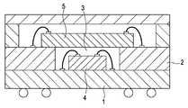
도 1은, 일본 특개 2002-353427호 공보에 개시된 이미지 센서의 스택 구조의 센서 패키지를 나타내는 도면.BRIEF DESCRIPTION OF THE DRAWINGS The figure which shows the sensor package of the stack structure of the image sensor disclosed by Unexamined-Japanese-Patent No. 2002-353427.
도 1의 센서 패키지 구조는, 제1 기판(1)의 제1 얼굴에 화형의 제2 기판(2)이 접합되어, 캐비티(3)가 형성된다.In the sensor package structure of FIG. 1, a
그 캐비티(3)의 제1 기판(1)의 제1면에 집적회로(4)가 장착되어 제2 기판(2)상에 이미지 센서 칩(5)이 접합되어 스택 구조의 센서 패키지가 형성된다.The integrated
그런데, 상술한 구조의 경우, 제조 프로세스상, 제1 기판(1)과 제2 기판(2)에 의해 캐비티(3)를 형성한 후에 집적회로(4)를 접합하여 쌓아올리는 식의 제조 프로세스로 한정되기 때문에, 이하의 불이익이 있다.By the way, in the above-described structure, in the manufacturing process, after the
즉, 동일 공정내에서의 쌓아올리는 것이 필요하기 때문에, 제조장소가 한정된다.That is, since it is necessary to stack | stack in the same process, a manufacturing place is limited.
또, 제조 과정에서 불량이 발생했을 경우, 예를 들어 이미지 센서의 밀봉시에 불량이 발생했을 경우는 스택 구조 센서 패키지를 구성하는 모두가 불량에 의해 폐기될 필요가 있어 불량 발생시의 폐기 비용이 비싸진다.In addition, when a defect occurs in the manufacturing process, for example, when a defect occurs during sealing of the image sensor, all of the stack structure sensor packages need to be discarded due to the defect, and the cost of disposal at the time of failure is expensive. Lose.
또, 상기 스택 구조의 센서 패키지를 제1 기판(1)의 이면 접합 단자에서 다른 구조체와 접합하는 경우, 일반적으로는 유기 기판과는 다 접속되는 경우가 많지만, 접합 개소가 아래쪽 면에 한정되어 있기 때문에, 접속 강도의 문제가 염려된다. 센서와 센서의 신호를 처리하는 집적회로(4)가 패키지화되고 있는 것으로, 그 외의 기능을 부가시키고 싶은 경우에 그 부가 기능을 실현하는 부품은 패키지의 밖에 추가로 배치할 필요가 있어, 소형화와 상반되어 버린다.In the case where the sensor package having the stack structure is bonded to another structure at the back bonding terminal of the
본 발명은, 제조 과정에서 불량이 발생했을 경우에도 센서 부품의 재이용이 가능해, 센서 부품의 접속 강도의 향상을 도모하고, 또한, 소형화, 박형화를 꾀하는 것이 가능한 다층 배선 기판, 스택 구조 센서 패키지 및 그 제조 방법을 제공하는 것에 있다.In the present invention, even when a defect occurs in the manufacturing process, the sensor component can be reused, the connection strength of the sensor component can be improved, and the multilayer wiring board, the stacked structure sensor package, which can be miniaturized and reduced in thickness can be obtained. It is providing the manufacturing method.
본 발명의 다층 배선 기판은, 제1면 및 제2면을 관통하는 관통 구멍을 갖고, 상기 제 1면 및 상기 제 2면 가운데 적어도 한편에, 상기 관통 구멍의 주연부인 내연부측, 기판 자체의 바깥 둘레부인 외연부측, 및 비가장자리부 가운데 적어도 1개에, 전기적 접속 단자가 형성되어 상기 전기적 접속 단자는, 형성면과 대향하는 측의 면에 관통하지 않는 축성(castellation) 구조를 가진다.The multilayer wiring board of this invention has the through-hole which penetrates a 1st surface and a 2nd surface, The inner periphery side which is a periphery of the said through hole, and at least one of the said 1st surface and said 2nd surface of the board | substrate itself At least one of the outer periphery side and the non-edge portion, which is the outer periphery, is provided with an electrical connection terminal, and the electrical connection terminal has a castellation structure that does not penetrate the surface on the side opposite to the forming surface.
본 발명의 다른 관점의 스택 구조 센서 패키지는, 관통 구멍을 갖고, 제1면에 와이어 본드용의 패드를 갖고, 제2면에 상기 관통 구멍의 주연부인 내연부측, 기판 자체의 바깥 둘레부인 외연부측, 및 비가장자리부 가운데 적어도 1개에, 전기적 접속 단자가 형성된 다층 배선 기판과 상기 다층 배선 기판의 상기 관통 구멍을 걸쳐 해당 다층 배선 기판의 상기 제 1면의 상기 관통 구멍의 주연부에 고정되어 상기 패드와 와이어로 전기적으로 접속된 이미지 센서와, 상기 다층 배선 기판의 상기 제 1면의 상기 외연부 측에 상기 이미지 센서를 둘러싸도록 고정된 프레임과, 상기 프레임의 표면에, 상기 이미지 센서와 대향하도록 고정된 광필터를 가진다.A stack structure sensor package according to another aspect of the present invention has a through hole, a pad for wire bonds on a first surface, an inner edge side of the periphery of the through hole, and an outer periphery of the substrate itself on a second surface. It is fixed to the peripheral part of the said through hole of the said 1st surface of the said multilayer wiring board through the multilayer wiring board in which the electrical connection terminal was formed, and the said through hole of the said multilayer wiring board in at least one of a side part and a non-edge part, An image sensor electrically connected to a pad and a wire, a frame fixed to surround the image sensor on the outer edge side of the first surface of the multilayer wiring board, and the surface of the frame to face the image sensor. It has a fixed optical filter.
본 발명의 또다른 관점의 스택 구조 센서 패키지의 제조 방법은, 관통 구멍을 갖고, 제1면에 와이어 본드용의 패드를 가져, 제2면에 상기 관통 구멍의 주연부인 내연부측, 기판 자체의 바깥 둘레부인 외연부측, 및 비가장자리부 가운데 적어도 1개에, 전기적 접속 단자가 형성된 다층 배선 기판의 상기 관통 구멍을 걸치도록, 해당 다층 배선 기판의 상기 제 1면의 상기 관통 구멍의 주연부에 이미지 센서를 고정하고, 상기 다층 배선 기판의 상기 패드와 상기 이미지 센서를 와이어로 전기적으로 접속하고, 상기 다층 배선 기판의 상기 제 1면의 상기 외연부 측에 상기 이미지 센서를 둘러싸도록 프레임을 고정하며, 상기 프레임의 표면에, 상기 이미지 센서와 대향하도록 광필터를 고정한다.A method of manufacturing a stack structure sensor package according to another aspect of the present invention includes a through hole, a pad for wire bonding on a first surface, and an inner edge side of the periphery of the through hole on a second surface, and a substrate itself. An image sensor at the periphery of the through hole of the first surface of the multilayer wiring board so as to cover the through hole of the multilayer wiring board on which the electrical connection terminal is formed on at least one of the outer edge portion and the non-edge portion, which is an outer periphery. Fixing the frame, electrically connecting the pad and the image sensor of the multilayer wiring board with wires, and fixing a frame to surround the image sensor on the outer edge side of the first surface of the multilayer wiring board, On the surface of the frame, an optical filter is fixed to face the image sensor.
본 발명에 의하면, 스택 구조를 가지는 센서 패키지의 제조 과정에서 불량이 발생했을 경우에도 센서 부품의 재이용이 가능해, 센서 부품의 접속 강도의 향상을 도, 또한, 소형화, 박형화를 꾀할 수가 있다.According to the present invention, even when a defect occurs in the manufacturing process of the sensor package having the stack structure, the sensor component can be reused, and the connection strength of the sensor component can be improved, and the size and thickness can be reduced.
도 1은 일본 특개 2002-353427호 공보에 개시된 이미지 센서의 스택 구조의 센서 패키지를 나타내는 도면.
도 2는 본 발명의 제1의 실시 형태와 관련되는 다층 배선 기판을 적용한 스택 구조 센서 패키지의 구조예를 나타내는 도면.
도 3은 본 실시 형태와 관련되는 다층 배선 기판의 제1의 구성예를 나타내는 도면.
도 4는 본 실시 형태와 관련되는 다층 배선 기판의 제2의 구성예를 나타내는 도면.
도 5는 본 실시 형태와 관련되는 다층 배선 기판의 제3의 구성예를 나타내는 도면.
도 6은 본 실시 형태와 관련되는 다층 배선 기판의 제4의 구성예를 나타내는 도면.
도 7은 본 실시 형태와 관련되는 다층 배선 기판의 제5의 구성예를 나타내는 도면.
도 8은 본 실시 형태와 관련되는 다층 배선 기판의 제6의 구성예를 나타내는 도면.
도 9는 본 실시 형태와 관련되는 다층 배선 기판의 제7의 구성예를 나타내는 도면.
도 10은 도 9의 다층 배선 기판을 기준으로서 도 6의 다층 배선 기판 및 도 3의 다층 배선 기판의 전극수 및 열충격에 대한 솔더 접속 강도에 대해 측정한 결과를 나타내는 도면.
도 11의 A 내지 D는 도 1의 스택 구조 센터 패키지의 제조 방법을 설명하기 위한 도면.
도 12는 본 발명의 제2의 실시 형태와 관련되는 다층 배선 기판을 적용한 스택 구조 센서 패키지의 구조예를 나타내는 도면.BRIEF DESCRIPTION OF THE DRAWINGS The figure which shows the sensor package of the stack structure of the image sensor disclosed by Unexamined-Japanese-Patent No. 2002-353427.
2 is a diagram showing a structural example of a stacked structure sensor package to which the multilayer wiring board according to the first embodiment of the present invention is applied.
3 is a diagram illustrating a first configuration example of a multilayer wiring board according to the present embodiment.
4 is a diagram illustrating a second configuration example of a multilayer wiring board according to the present embodiment.
FIG. 5 is a diagram showing a third structural example of the multilayer wiring board according to the present embodiment. FIG.
FIG. 6 is a diagram showing a fourth structural example of the multilayer wiring board according to the present embodiment. FIG.
7 is a diagram showing a fifth structural example of the multilayer wiring board according to the present embodiment.
8 is a diagram showing a sixth structural example of the multilayer wiring board according to the present embodiment.
9 is a diagram illustrating a seventh configuration example of the multilayer wiring board according to the present embodiment.
FIG. 10 is a view showing the results of measurement of solder connection strength against the number of electrodes and thermal shock of the multilayer wiring board of FIG. 6 and the multilayer wiring board of FIG. 3 with reference to the multilayer wiring board of FIG. 9.
11A to 11D illustrate a method of manufacturing the stack structure center package of FIG. 1.
It is a figure which shows the structural example of the stack structure sensor package which applied the multilayer wiring board which concerns on 2nd Embodiment of this invention.
이하, 본 발명의 실시 형태를 도면에 관련지어 설명한다. 덧붙여 설명은 이하의 순서로 실시한다.EMBODIMENT OF THE INVENTION Hereinafter, embodiment of this invention is described with reference to drawings. In addition, description is given in the following procedure.
1. 제1의 실시 형태1. First embodiment
2. 제2의 실시 형태2. Second Embodiment
<1. 제1의 실시 형태><1. First embodiment>
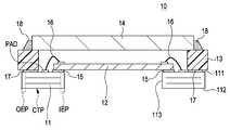
도 2는, 본 발명의 제1의 실시 형태와 관련되는 다층 배선 기판을 적용한 스택 구조 센서 패키지의 구조예를 나타내는 도면.The figure which shows the structural example of the stack structure sensor package to which the multilayer wiring board which concerns on 1st Embodiment of this invention was applied.
센서 패키지(10)는, 기본적으로, 다층 배선 기판(11), 이미지 센서 칩(12), 세라믹스나 수지등에 의해 형성되는 프레임(13), 및 광필터(14)를 주구성 요소로 한 스택 구조를 가지고 있다.The
다층 배선 기판(11)은, 이미지 센서의 스택 구조 센서 패키지(10)의 기체가 되는 기판으로, 이하에 설명하는 특징적인 구성을 가지고 있다.The
다층 배선 기판(11)은, 중앙부에, 제1면(표면)(111) 및 제2면(이면)(112)를 관통하는 관통 구멍(113)이 형성되고 있다.In the
다층 배선 기판(11)은, 제1면(111) 및 제2면(112) 가운데 적어도 한편에 관통 구멍(113)의 주연부인 내연부(IEP)측, 기판 자체의 바깥 둘레부인 외연부(OEP)가, 및 비가장자리부 가운데 적어도 1개에, 전기적 접속 단자(전극)가 형성되고 있다.The
다층 배선 기판(11)은, 이 내연부(IEP), 및 외연부(OEP)의 적어도 한편에 형성되는 전기적 접속 단자(전극)는, 이하에 설명하는 바와 같이, 형성면과 대향하는 측의 면에 관통하지 않는(도달하지 않는다) 축성(디프레션) 구조를 가진다.As for the
이 내연부(IEP), 및 외연부(OEP)의 적어도 한편에 형성되는 전기적 접속 단자(전극)는, 다른 기판등과의 접속 강도를 향상시키기 위해 형성된다.Electrical connection terminals (electrodes) formed on at least one of the inner edge portion IEP and the outer edge portion OEP are formed to improve the connection strength with other substrates.
또, 내연부(IEP), 및 외연부(OEP)의 적어도 한편에 형성되는 전기적 접속 단자(전극)가 가지는 축성 구조는, 접속 강도의 향상을 꾀해, 또, 외부등으로부터 전극에 참가하는 응력을 완화하는 기능을 가지고 있다.In addition, the layered structure of the electrical connection terminal (electrode) formed on at least one of the inner edge portion IEP and the outer edge portion OEP is intended to improve the strength of the connection, and also to prevent stress from participating in the electrode from the outside. It has a mitigating function.
도 2에 나타내는 다층 배선 기판(11)에서는, 제1면(111)의 내연부(IEP)와 외연부(OEP)간의 중앙부에 와이어 본딩용의 패드(PAD)가 형성되어 제2면(112)의 내연부(IEP), 및 외연부(OEP)의 적어도 한편에 전기적 접속 단자(전극)가 형성된다.In the
또, 다층 배선 기판(11)의 제2면(112) 측에는 내연부(IEP)와 외연부(OEP)와의 사이의 중앙부 CTP에도 접속 단자(내부 전극)가 형성된다.In addition, a connection terminal (inner electrode) is also formed in the central portion CTP between the inner edge portion IEP and the outer edge portion OEP on the
이하, 다층 배선 기판(11)의 것보다 구체적인 구성예에 대해, 도면에 관련지어 설명한다.Hereinafter, the specific structural example rather than the thing of the
[다층 배선 기판의 제1의 구성예][1st structural example of a multilayer wiring board]
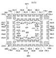
도 3은, 본 실시 형태와 관련되는 다층 배선 기판의 제1의 구성예를 나타내는 도면이다.3 is a diagram showing a first structural example of the multilayer wiring board according to the present embodiment.
도 3은, 다층 배선 기판(11)의 제2면(이면)(112)측의 구성예를 나타내고 있다.3 shows an example of the configuration of the second surface (rear surface) 112 side of the
도 3의 다층 배선 기판(11A)은, 전체적으로 직방체(구형)로서 형성되고 있다.The
다층 배선 기판(11A)은, 전술한 것처럼, 중앙부에, 제1면(표면)(111) 및 제2면(이면)(112)를 관통하는 관통 구멍(113)이 형성되고 있다.As described above, in the
도 3의 다층 배선 기판(11A)은, 제2면(이면)(112)에, 관통 구멍(113)의 주연부인 내연부(IEP1, IEP2, IEP3, IEP4)의 모두에 제1의 전기적 접속 단자(이하, 내주 전극이라고 한다)(IEL)가 형성되고 있다.The
또한, 도 3의 다층 배선 기판(11A)은, 기판 자체의 바깥 둘레부인 외연부(OEP1, OEP2, PEP3, OEP4)의 모두에 제2의 전기적 접속 단자(이하, 외주 전극이라고 한다)(OEL)가 형성되고 있다.In addition, the
또한, 도 3의 다층 배선 기판(11A)은, 기판의 바깥 둘레부의 4코너(CNR1, CNR2, CNR3, CNR4)에도, 외주 전극에 포함되는 전기적 접속 단자(이하, 코너 전극)(OCEL1, OCEL2, OCEL3, OCEL4)가 형성되고 있다.In addition, the
또, 도 3의 다층 배선 기판(11A)은, 내연부(IEP1)와 외연부(OEP1)와의 사이, 및 내연부(IEP3)와 외연부(OEP3)와의 사이의 비가장자리부(내부)에 제3의 전기적 접속 단자(이하, 내부 전극이라고 한다)(CTEL1, CTEL2, CTEL3, CTEL4)가 형성되고 있다.In addition, the
덧붙여 본 실시 형태로 가리키는 내주 전극(IEL), 외주 전극(OEL), 및 내부 전극(CTEL)의 형성수는, 어디까지나 일례이며, 이해를 용이하게 하기 위해서 몇 개로 하고 있지만, 실제는, 도시하는 전극의 수로 한정되지 않고, 그 수는 사용 용도에 의해 적당 설정된다.In addition, the number of formation of the inner circumferential electrode IEL, the outer circumferential electrode OEL, and the inner electrode CTEL indicated by this embodiment is an example to the last, and it is set as some in order to make understanding easy, but actually shows It is not limited to the number of electrodes, The number is suitably set according to a use use.
도 3에 대해, 내연부(IEP1)에는, 내주 전극(IEL11, IEL12, IEL13, IEL14, IEL15, IEL16)이 형성되고 있다.3, inner peripheral electrodes IEL11, IEL12, IEL13, IEL14, IEL15, and IEL16 are formed in the inner edge part IEP1.
내주 전극(IEL11, IEL12, IEL13, IEL14, IEL15, IEL16)은 관통 구멍(113)에 접하는 측부가 원호상으로 일부 함몰된 축성 구조를 가지도록 형성되고 있다.The inner circumferential electrodes IEL11, IEL12, IEL13, IEL14, IEL15, and IEL16 are formed to have a layered structure in which the side portion in contact with the through
내연부(IEP2)에는, 내주 전극(IEL21, IEL22, IEL23, IEL24, IEL25)이 형성되고 있다.The inner circumferential electrodes IEL21, IEL22, IEL23, IEL24, and IEL25 are formed in the inner edge portion IEP2.
내주 전극(IEL21, IEL22, IEL23, IEL24, IEL25)은, 관통 구멍(113)에 접하는 측부가 원호상으로 일부 함몰된 축성 구조를 가지도록 형성되고 있다.The inner circumferential electrodes IEL21, IEL22, IEL23, IEL24, and IEL25 are formed to have a layered structure in which the side portion in contact with the through
내연부(IEP3)에는, 내주 전극(IEL31, IEL32, IEL33, IEL34, IEL35, IEL36)이 형성되고 있다.In the inner edge part IEP3, the inner peripheral electrodes IEL31, IEL32, IEL33, IEL34, IEL35, and IEL36 are formed.
내주 전극(IEL31, IEL32, IEL33, IEL34, IEL35, IEL36)은, 관통 구멍(113)에 접하는 측부가 원호상으로 일부 함몰된 축성 구조를 가지도록 형성되고 있다.The inner circumferential electrodes IEL31, IEL32, IEL33, IEL34, IEL35, and IEL36 are formed to have a layered structure in which the side portion in contact with the through
내연부(IEP4)에는, 내주 전극(IEL41, IEL42, IEL43, IEL44, IEL45)이 형성되고 있다.The inner peripheral electrodes IEL41, IEL42, IEL43, IEL44, and IEL45 are formed in the inner edge portion IEP4.
내주 전극(IEL41, IEL42, IEL43, IEL44, IEL45)은, 관통 구멍(113)에 접하는 측부가 원호상으로 일부 함몰된 축성 구조를 가지도록 형성되고 있다.The inner circumferential electrodes IEL41, IEL42, IEL43, IEL44, and IEL45 are formed to have a layered structure in which the side portion in contact with the through
도 3에 대해, 외연부(OEP1)에는, 외주 전극(OEL11, OEL12, OEL13, OEL14, OEL15, OEL16, OEL16, OEL17, OEL18)이 형성되고 있다.3, outer electrode OEL11, OEL12, OEL13, OEL14, OEL15, OEL16, OEL16, OEL17, OEL18 are formed in outer edge part OEP1.
외주 전극(OEL11, OEL12, OEL13, OEL14, OEL15, OEL16, OEL17, OEL18)은, 외부에 접하는 측부가 원호상으로 일부 함몰된 축성 구조를 가지도록 형성되고 있다.The outer circumferential electrodes OEL11, OEL12, OEL13, OEL14, OEL15, OEL16, OEL17, OEL18 are formed so as to have a layered structure in which the side contacting the outside is partially recessed in an arc shape.
외연부(OEP2)에는, 외주 전극(OEL21, OEL22, OEL23, OEL24, OEL25)이 형성되고 있다.In the outer edge part OEP2, outer peripheral electrodes OEL21, OEL22, OEL23, OEL24, and OEL25 are formed.
외주 전극(OEL21, OEL22, OEL23, OEL24, OEL25)은, 외부에 접하는 측부가 원호상으로 일부 함몰된 축성 구조를 가지도록 형성되고 있다.The outer circumferential electrodes OEL21, OEL22, OEL23, OEL24, and OEL25 are formed to have a layered structure in which the side portions in contact with the outside are recessed in a circular arc shape.
외연부(OEP3)에는, 외주 전극(OEL31, OEL32, OEL33, OEL34, OEL35, OEL36, OEL36, OEL37, OEL38)가 형성되고 있다.In the outer edge portion OEP3, outer electrodes OEL31, OEL32, OEL33, OEL34, OEL35, OEL36, OEL36, OEL37, and OEL38 are formed.
외주 전극(OEL31, OEL32, OEL33, OEL34, OEL35, OEL36, OEL36, OEL37, OEL38)는, 외부에 접하는 측부가 원호상으로 일부 함몰된 축성 구조를 가지도록 형성되고 있다.The outer circumferential electrodes OEL31, OEL32, OEL33, OEL34, OEL35, OEL36, OEL36, OEL37, and OEL38 are formed so as to have a layered structure in which the side contacting the outside is recessed in an arc shape.
외연부(OEP4)에는, 외주 전극(OEL41, OEL42, OEL43, OEL44, OEL45)이 형성되고 있다.In the outer edge part OEP4, outer electrode OEL41, OEL42, OEL43, OEL44, OEL45 is formed.
외주 전극(OEL41, OEL42, OEL43, OEL44, OEL45)은, 외부에 접하는 측부가 원호상으로 일부 함몰된 축성 구조를 가지도록 형성되고 있다.The outer circumferential electrodes OEL41, OEL42, OEL43, OEL44, and OEL45 are formed to have a layered structure in which the side portions in contact with the outside are recessed in an arc shape.
또, 코너 전극(OCEL1, OCEL2, OCEL3, OCEL4)도, 외부에 접하는 측부가 원호상으로 일부 함몰된 축성 구조를 가지도록 형성되고 있다.In addition, the corner electrodes OCEL1, OCEL2, OCEL3, and OCEL4 are also formed to have a layered structure in which side portions in contact with the outside are recessed in an arc shape.
이와 같이, 도 3의 다층 배선 기판(11A)은, 제2면(이면)(112)에, 관통 구멍(113)의 주연부인 내연부(IEP1, IEP2, IEP3, IEP4)의 모두에 내주 전극(IEL)가 형성되고 있다.Thus, the
또한, 도 3의 다층 배선 기판(11A)은, 기판 자체의 바깥 둘레부인 외연부(OEP1, OEP2, PEP3, OEP4)의 모두에 외주 전극(OEL)가 형성되고 있다.In addition, in the
또한, 도 3의 다층 배선 기판(11A)은, 기판의 바깥 둘레부의 4코너(CNR1, CNR2, CNR3, CNR4)의 모두에도, 코너 전극(OCEL1, OCEL2, OCEL3, OCEL4)가 형성되고 있다.In addition, in the
그리고, 이러한 전극은 축성 구조를 가지는 것으로부터, 후술하는 바와 같이, 가장자리에 전극이 없는 경우 등과 비교해, 전극수가 증대될 수 있고, 열충격에 대한 솔더 접속 강도 등이 높아지고 있다.Since the electrodes have a layered structure, as described below, the number of electrodes can be increased, and the solder connection strength with respect to thermal shock is increased, as compared with the case where there is no electrode at the edge.
또, 도 3의 다층 배선 기판(11A)은, 다층 배선 기판(11A)이 다른 다층 배선 기판과 접합하는 경우에, 접합부의 검사를 눈으로 실시 가능으로 하는 경우에 유효한 형상이며, 검사성을 고려해 전극이 배치되어 있다.In addition, when the
[다층 배선 기판의 제2의 구성예][2nd structural example of a multilayer wiring board]
도 4는, 본 실시 형태와 관련되는 다층 배선 기판의 제2의 구성예를 나타내는 도면이다.4 is a diagram illustrating a second configuration example of the multilayer wiring board according to the present embodiment.
도 4는, 다층 배선 기판(11B)의 제2면(이면)(112)측의 구성예를 나타내고 있다.4 illustrates a configuration example of the second surface (back surface) 112 side of the
도 4의 다층 배선 기판(11B)이 도 3의 다층 배선 기판(11A)과 기본적으로 다른 점은, 내부 전극(CTEL1, CTEL2, CTEL3, CTEL4)가 형성되어 있지 않은 것에 있다.The basic difference from the
덧붙여 도 4의 다층 배선 기판(11B)에 대해서는, 내연부(IEP2)에는, 3개의 내주 전극(IEL21, IEL22, IEL23)이 형성되고 있다. 또, 내연부(IEP4)는, 내주 전극(IEL41, IEL42, IEL43)이 형성되고 있다.In addition, about the
이 도 4의 다층 배선 기판(11B)나, 다른 다층 배선 기판과 접합하는 경우에, 접합부의 검사를 눈으로 실시 가능한 경우의 형상이며, 검사성을 고려한 전극 배치가 되고 있다.When joining with this
그리고, 다층 배선 기판(11B)은, 가장자리에 전극이 없는 경우 등과 비교하여, 전극수를 증대시킬 수 있고 , 열충격에 대한 솔더 접속 강도등이 높아지고 있다.And compared with the case where there is no electrode in the edge, etc., in the
[다층 배선 기판의 제3의 구성예][Third structural example of multilayer wiring board]
도 5는, 본 실시 형태와 관련되는 다층 배선 기판의 제3의 구성예를 나타내는 도면이다.FIG. 5: is a figure which shows the 3rd structural example of the multilayer wiring board which concerns on this embodiment.
도 5는, 다층 배선 기판(11C)의 제2면(이면)(112)측의 구성예를 나타내고 있다.5 shows an example of the configuration of the second surface (back side) 112 side of the
도 5의 다층 배선 기판(11C)이 도 3의 다층 배선 기판(11A)와 기본적으로 다른 점은 이하와 같다.The
다층 배선 기판(11C)은, 내연부(IEP2, IEP4)에 내주 전극이 형성되지 않고, 내연부(IEP2)와 외연부(OEP2)와의 사이, 내연부(IEP4)와 외연부(OEP4)와의 사이의 비가장자리부에 내부 전극(CTEL)가 복수(도 5에서는 5개씩) 형성되고 있다.In the
다층 배선 기판(11C)은, 가장자리에 전극이 없는 경우등과 비교하여, 전극수가 증대될 수 있고, 열충격에 대한 솔더 접속 강도 등이 높아지고 있다.In the
[다층 배선 기판의 제4의 구성예]Fourth structural example of a multilayer wiring board
도 6은, 본 실시 형태와 관련되는 다층 배선 기판의 제4의 구성예를 나타내는 도면이다.6 is a diagram showing a fourth structural example of the multilayer wiring board according to the present embodiment.
도 6은, 다층 배선 기판(11D)의 제2면(이면)(112)측의 구성예를 나타내고 있다.6 shows an example of the configuration of the second surface (back side) 112 side of the
도 6의 다층 배선 기판(11D)이 도 5의 다층 배선 기판(11C)과 기본적으로 다른 점은 이하와 같다.The point that the
다층 배선 기판(11D)은, 내연부(IEP1, IEP2, IEP3, IEP4)의 모두에 내주 전극이 형성되어 있지 않다.In the
이 다층 배선 기판(11D)은, 다른 다층 배선 기판과 접합하는 경우에, 관통 구멍(113)을 최대한으로 크게 할 수 있어 관통 구멍(113)의 내부 측에 둘 수 있는 실장 면적을 최대로 하는 경우에 유효한 형상이다. 다층 배선 기판(11D)나, 가장자리에 전극이 없는 경우 등과 비교하여, 전극수가 증대될 수 있고, 열충격에 대한 솔더 접속 강도 등이 높아지고 있다.When the
[다층 배선 기판의 제5의 구성예][Fifth structural example of multilayer wiring board]
도 7은, 본 실시 형태와 관련되는 다층 배선 기판의 제5의 구성예를 나타내는 도면이다.FIG. 7: is a figure which shows the 5th structural example of the multilayer wiring board which concerns on this embodiment.
도 7은, 다층 배선 기판(11E)의 제2면(이면)(112)측의 구성예를 나타내고 있다.7 shows an example of the configuration of the second surface (back side) 112 side of the
도 7의 다층 배선 기판(11E)이 도 5의 다층 배선 기판(11C)과 기본적으로 다른 점은 이하와 같다.The difference of the
다층 배선 기판(11E)은, 내연부(IEP2, IEP4)에 내주 전극이 형성되지 않고, 한편 외연부(OEP1~OEP4)의 모두에 외주 전극이 형성되지 않고, 비가장자리부 전체에 걸쳐서 접속용의 내부 전극에 내부 전극(CTEL)이 복수(도 7에서는 42개) 형성되고 있다.In the
이 다층 배선 기판(11E)은, 다른 다층 배선 기판과 접합하는 경우에, 접속용의 단자수를 늘릴 필요가 있어, 한편 그 실장 면적을 본 실시 형태의 다층 배선 기판의 외형과 동등하게 하는 경우에 유효한 형상이다.In the case where the
또, 다층 배선 기판(11E)은, 가장자리에 전극이 없는 경우등과 비교해, 전극수가 증대될 수 있고, 열충격에 대한 솔더 접속 강도 등이 높아지고 있다.In addition, the number of electrodes can be increased, and the solder connection strength with respect to thermal shock is increased in the
[다층 배선 기판의 제6의 구성예][Sixth structural example of multilayer wiring board]
도 8은, 본 실시 형태와 관련되는 다층 배선 기판의 제6의 구성예를 나타내는 도면이다.8 is a diagram illustrating a sixth configuration example of the multilayer wiring board according to the present embodiment.
도 8은, 다층 배선 기판(11F)의 제2면(이면)(112)측의 구성예를 나타내고 있다.8 illustrates a configuration example of the second surface (back surface) 112 side of the
도 8의 다층 배선 기판(11F)이 도 4의 다층 배선 기판(11B)과 기본적으로 다른 점은 이하와 같다.The point that the
다층 배선 기판(11F)은, 외연부(OEP1~OEP4)의 모두에 외주 전극이 형성되지 않고, 비가장자리부 전체에 걸쳐서 접속용의 내부 전극이 형성되어 있지 않다.In the
다층 배선 기판(11F)은, 가장자리에 전극이 없는 경우등과 비교해, 전극수가 증대될 수 있고, 열충격에 대한 솔더 접속 강도 등이 높아지고 있다.In the
[다층 배선 기판의 제7의 구성예][Seventh structural example of multilayer wiring board]
도 9는, 본 실시 형태와 관련되는 다층 배선 기판의 제7의 구성예를 나타내는 도면이다.9 is a diagram illustrating a seventh structural example of the multilayer wiring board according to the present embodiment.
도 9는, 다층 배선 기판(11G)의 제2면(이면)(112)측의 구성예를 나타내고 있다.9 shows an example of the configuration of the second surface (back surface) 112 side of the
도 9의 다층 배선 기판(11G)이 도 6의 다층 배선 기판(11D)과 기본적으로 다른 점은 이하와 같다.The difference of the
다층 배선 기판(11G)은, 외연부(OEP1~OEP4)의 모두에 외주 전극이 형성되지 않고, 비가장자리부 전체에 걸쳐서 접속용의 내부 전극이 복수 형성되고 있다.In the
다층 배선 기판(11G)은, 다른 다층 배선 기판과 접합하는 경우에, 그 실장 면적을 최소로 하는 경우에 유효한 형상이다.When the
다층 배선 기판(11G)은, 접속 강도의 점에서는, 제1~제6의 구성예에 비해 낮아지지만, 내부 전극수의 증대를 꾀할 수 있다.The
여기서, 도 9의 다층 배선 기판(11G)을 기준으로서 도 6의 다층 배선 기판(11D) 및 도 3의 다층 배선 기판(11A)의 전극수 및 열충격에 대한 솔더 강도에 대해 고찰한다.Here, the solder strength with respect to the number of electrodes and thermal shock of the
도 10은, 도 9의 다층 배선 기판을 기준으로서 도 6의 다층 배선 기판 및 도 3의 다층 배선 기판의 전극수 및 열충격에 대한 솔더강도에 대해 측정한 결과를 나타내는 도면이다.FIG. 10 is a diagram showing the results of measuring the solder strength against the number of electrodes and thermal shock of the multilayer wiring board of FIG. 6 and the multilayer wiring board of FIG. 3 with reference to the multilayer wiring board of FIG. 9.
도 10에 대해, 접속 강도는, 도 9의 다층 배선 기판(11G)을 기준(기본 패턴) 1일 때의, 테스트 부분에서 실측한 값을 비율로 가리키고 있다.In FIG. 10, the connection strength indicates the value measured in the test portion when the
이 경우, 도 6의 다층 배선 기판(11D)의 접속 강도는, 기본 패턴인 도 9의 다층 배선 기판(11G)의 1.71배이다.In this case, the connection strength of the
도 3의 다층 배선 기판(11A)의 접속 강도는, 기본 패턴인 도 9의 다층 배선 기판(11G)의 1.64배이다.The connection strength of the
또, 전극수는, 도 9의 다층 배선 기판(11G)의 수를 40으로 했을 경우, 도 6의 다층 배선 기판(11D)의 접속 강도는, 기본 패턴인 도 9의 다층 배선 기판(11G)의 1.4배인 56이다.Moreover, when the number of electrodes makes 40 the number of the
도 3의 다층 배선 기판(11A)의 접속 강도는, 기본 패턴인 도 9의 다층 배선 기판(11G)의 1.4배인 56이다.The connection strength of the
이상과 같이, 본 실시 형태의 다층 배선 기판(11, 11A~11F)는, 중앙부에, 제1면(표면)(111) 및 제2면(이면)(112)을 관통하는 관통 구멍(113)이 형성되고 있다.As described above, the
다층 배선 기판(11)은, 제1면(111) 및 제2면(112) 가운데 적어도 한편에 관통 구멍(113)의 주연부인 내연부(IEP)측, 기판 자체의 바깥 둘레부인 외연부(OEP)측, 및 비가장자리부 가운데 적어도 1개에, 전기적 접속 단자(전극)가 형성되고 있다.The
다층 배선 기판(11)은, 이 내연부(IEP), 및 외연부(OEP)의 적어도 한편에 형성되는 전기적 접속 단자(전극)는, 형성면과 대향하는 측의 면에 관통하지 않는(도달하지 않는) 축성(디프레션) 구조를 가진다.In the
따라서, 다층 배선 기판(11, 11A~11F)는, 다른 기판등과의 접속 강도를 향상시킬 수가 있어 또, 전극수(단자수)도 증대시킬 수가 있다.Therefore, the
또, 다층 배선 기판(11G)은, 다른 다층 배선 기판과 접합하는 경우에, 그 실장 면적을 최소로 할 수 있다.In addition, when the
이러한 특징을 가지는 다층 배선 기판(11, 11A~11G)를 이용한 도 2의 스택 구조 센터 패키지(10)는, 그 제조 과정에서 불량이 발생했을 경우에도 센서 부품의 재이용을 가능해, 센서 부품의 접속 강도의 향상을 도모하고, 소형화, 박형화를 꾀하는 것이 가능해진다.The stack
도 11의 (A)~(D)는, 도 1의 스택 구조 센터 패키지(10)의 제조 방법을 설명하기 위한 도면이다.FIG. 11: (A)-(D) is a figure for demonstrating the manufacturing method of the stack
여기서, 도 1의 스택 구조 센터 패키지(10)의 제조 방법에 대해, 도 11의 (A)~(D)에 대응하여 설명한다.Here, the manufacturing method of the stack
우선, 관통 구멍(113)을 갖고, 제1면(표면)(111)에 와이어 본드용의 패드(PAD), 제2면(이면)(112)에 타기판과의 접속용 전극(IEP, OEP, CTEL)의 적어도 어느 쪽을 포함한 다층 배선 기판(1)의 표면에 이미지 센서(12)를 접착제(15)로 고정한다.First, the through
다음에, 도 11의 (B)에 도시된 바와 같이, 이미지 센서(12)로 다층 배선 기판(11)의 패드(PAD)를 와이어(16)에 의해 전기적으로 접속한다.Next, as shown in FIG. 11B, the pad PAD of the
다음에, 도 11의 (C)에 도시된 바와 같이, 다층 배선 기판(11)의 제1면(표면)(111)에 이미지 센서(12)를 둘러싸도록 프레임(13)을 접착제(17)로 고정한다.Next, as shown in FIG. 11C, the
그리고, 도 11의 (D)에 도시된 바와 같이, 세라믹스나 수지등에 의해 형성되는 프레임(13)의 표면에 광학 필터(14)를 접착제(18)로 접착해 밀봉한다.As shown in FIG. 11D, the
이상에 의해, 이미지 센서 부품으로서의, 도 1의 스택 구조 센터 패키지(10)의 제조가 완료한다.By the above, manufacture of the stack
이와 같이 제조되는 도 1의 스택 구조 센터 패키지(10)는, 제조 과정에서 불량이 발생했을 경우에도 센서 부품의 재이용을 가능해, 센서 부품의 접속 강도의 향상을 도모하고, 소형화, 박형화를 꾀하는 것이 가능해진다.The stack
<2. 제2의 실시 형태><2. Second embodiment>
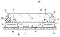
도 12는, 본 발명의 제2의 실시 형태와 관련되는 다층 배선 기판을 적용한 스택 구조 센서 패키지의 구조예를 나타내는 도면.The figure which shows the structural example of the stack structure sensor package to which the multilayer wiring board which concerns on 2nd Embodiment of this invention was applied.
제 2의 실시 형태와 관련되는 스택 구조 센서 패키지(10A)가 제1의 실시 형태의 센서 패키지(10)와 다른 점은, 이하와 같다.The stack
스택 구조 센서 패키지(10A)는, 다층 배선 기판(11)의 제2면(이면)(112) 측에, 전자 디바이스, 예를 들어 집적회로(21), 저항등의 전자 부품(22)이 탑재된 유기 다층 기판(20)을 전술한 접속 단자(전극)에 의해 솔더(24)로 접속되고 있다.The stack
스택 구조 센서 패키지(10A)는, 상술한 것처럼, 도 1의 이미지 센서 부품이 제조된 후, 이하의 제조 공정을 거쳐 형성된다.As described above, the stack
다층 배선 기판(11) 이외의 다른 유기 다층 기판(20)상에, 집적회로(21) 및 전자 부품을 탑재하고, 이것들을 가리도록 상기 이미지 센서 부품(10)을 씌워 동시에 솔더 접합하는 것으로써 스택 구조를 가지는 센서 패키지(10A)로 한다.On the
이상, 제1 및 제2의 실시 형태와 관련되는 스택 구조 센서 패키지(10, 10A)에 대해 설명하였다.In the above, the stack
상기 설명으로, 도 3~도 9은, 전극 배치의 형상예이며, 전극수, 전극간 피치, 전극 사이즈는 용도에 응해 변경하는 것으로 한다. 또, 다층 배선 기판(11) 및 관통 구멍(113)의 형상도 용도에 응해 변경하는 것으로 한다.In the above description, FIGS. 3 to 9 are examples of shapes of electrode arrangement, and the number of electrodes, the pitch between electrodes, and the electrode size are changed depending on the application. In addition, the shape of the
다층 배선 기판(11)은, 유기 기판, 무기 기판 어디라도 가능으로 한다.The
다층 배선 기판(11)의 전극 도금은, 동패턴, 금도금 처리, 방수 처리라도 좋다.Electrode plating of the
또, 본 실시 형태의 반도체 장치 아래에 실장하는 부품은 능동 부품, 수동 부품이라도 좋다.In addition, the component mounted under the semiconductor device of this embodiment may be an active component or a passive component.
이상 설명한 것처럼, 본 실시 형태에 의하면, 센서 부품에 관통 구멍(113)을 갖는 다층 배선 기판(11)을 이용한다.As explained above, according to this embodiment, the
그 결과, 개별 공정에서 센서 패키지의 동작에 필요한 전자 부품·집적회로와 패키지할 때에, 센서 부품하에 그러한 전자 부품·집적회로를 배치하는 것이 가능해진다.As a result, when packaging with an electronic component and integrated circuit required for the operation of the sensor package in a separate process, it becomes possible to arrange such an electronic component and integrated circuit under the sensor component.
또, 한층 더 그러한 부품과 함께 센서 부품도 동시에 솔더 접합하는 것이 가능한 것으로 스택 구조 센서 패키지를 형성하는 제조 방법을 취하는 것으로, 이하의 효과를 얻는 것이 가능해진다.Moreover, it is possible to solder-bond a sensor component together with such a component simultaneously, and by taking the manufacturing method which forms a stack structure sensor package, the following effects can be acquired.
관통 구멍(113)을 갖는 다층 배선 기판(11)을 이용하는 것으로, 기판 아래쪽 면은 물론, 기판 외주 및 관통 구멍 내주에도 접속용 단자를 마련할 수가 있다. 한편, 단자를 축성 구조로 하는 것은 다 접합하는 경우에 피렛트를 형성할 수 있는 것으로 유기 다층 기반과 센서 패키지(센서 부품)의 접합 강도를 향상할 수 있다.By using the
관통 구멍(113)을 갖는 다층 배선 기판(11)을 가지는 센서 패키지를 부품으로서 취급하는 것으로, 일반의 실장 설비에서 스택 구조의 센서 패키지의 제조를 할 수 있기 때문에, 제조장소를 선택할 필요가 없게 제조 프로세스에 범용성을 갖게하는 것이 가능하다.By treating the sensor package having the
관통 구멍(113)을 갖는 다층 배선 기판(11)이 실장된 센서 패키지를 부품으로서 취급하는 것으로, 센서하에 배치하는 전자 부품·집적회로와 함께 솔더 접합하는 것이 가능하다. 이 때문에, 스택 구조 센서 패키지를 간단한 프로세스로 제조하는 것이 가능하다.By treating the sensor package mounted with the
관통 구멍(113)을 갖는 다층 배선 기판(11)을 실장한 센서 패키지하에 배치하는 부품은 솔더 접합이 가능한 것으로부터, 집적회로에 한정하지 않고 다종의 부품을 이용할 수가 있기 때문에 자유도가 더해, 스택 구조 센서 패키지의 성능을 향상시킬 수가 있다.The parts disposed under the sensor package in which the
관통 구멍(113)을 갖는 다층 배선 기판(11)을 실장한 센서 패키지는, 그 아래에 배치되는 전자 부품·집적회로와 별공정으로 제조된다. 이 때문에, 센서 부품의 제조 과정에 대해 불량이 발생했을 경우, 폐기 코스트는 센서 부품만이 대상이 되기 때문에, 불량 발생시의 폐기 코스트를 삭감할 수가 있다. 또, 센서 패키지 제조 과정에서 불량이 발생했을 경우는, 센서 부품은 재이용하는 것으로, 폐기 코스트를 억제하는 것이 가능하다.The sensor package in which the
본 발명은 일본 특허출원 JP2009-083658호(2009.03.30)의 우선권 주장 출원이다.This invention is a priority claim application of Japanese patent application JP2009-083658 (2009.03.30).
본 발명은 첨부된 청구범위 내에서 당업자에 의해 필요에 따라 다양하게 변형, 변경, 조합, 대체 등이 이루어질 수 있다.The present invention may be variously modified, changed, combined, replaced, etc. as necessary by those skilled in the art within the scope of the appended claims.
Claims (9)
Translated fromKorean상기 제1면으로부터 제2면을 관통하는 관통 구멍; 및
상기 제 1면 및 상기 제 2면 중 적어도 한 쪽에, 상기 관통 구멍의 둘레부인 내연부측, 기판 자체의 바깥 둘레부인 외연부측, 및 비가장자리부 중 적어도 1개에 형성된 전기적 접속 단자를 포함하고,
상기 전기적 접속 단자는, 형성면과 대향하는 측의 면을 통해 관통하지 않는 축성 구조를 가지는 것을 특징으로 하는 다층 배선 기판.In the multilayer wiring board which has a 1st surface and a 2nd surface,
A through hole penetrating the second surface from the first surface; And
An electrical connection terminal formed on at least one of the first surface and the second surface, formed on at least one of an inner edge portion of the through hole, an outer edge portion of the outer periphery of the substrate itself, and a non-edge portion;
The electrical connection terminal has a layered structure that does not penetrate through a surface on the side opposite to the formation surface.
상기 내연부와 상기 외연부 중에서 적어도 상기 외연부에 상기 전기적 접속 단자가 형성되어 있는 것을 특징으로 하는 다층 배선 기판.The method of claim 1,
The electrical wiring terminal is formed in at least the said outer edge part among the said inner edge part and the said outer edge part, The multilayer wiring board characterized by the above-mentioned.
상기 내연부와 상기 외연부 사이의 비가장자리부에, 전기적 내부 접속 단자가 형성되어 있는 것을 특징으로 하는 다층 배선 기판.3. The method according to claim 1 or 2,
An electric internal connection terminal is formed in a non-edge portion between the inner edge portion and the outer edge portion.
상기 다층 배선 기판의 상기 관통 구멍을 걸쳐 상기 다층 배선 기판의 상기 제 1면 상의 상기 관통 구멍의 주연부에 고정되어, 와이어로 상기 패드에 전기적으로 접속되는 이미지 센서;
상기 다층 배선 기판의 상기 제 1면의 상기 외연부 측에 고정되어 상기 이미지 센서를 둘러싸는 프레임; 및
상기 프레임의 표면에 고정되어 상기 이미지 센서와 대향하는 광필터를 가지며,
상기 전기적 접속 단자는, 상기 관통 구멍의 주연부인 내연부측, 기판의 바깥 둘레부인 외연부측, 및 비가장자리부 중 적어도 1개에 형성되는 것을 특징으로 하는 스택 구조 센서 패키지.A multilayer wiring board having a through hole and including a pad for wire bonding on a first surface and an electrical connection terminal on a second surface;
An image sensor fixed to a periphery of the through hole on the first surface of the multilayer wiring board over the through hole of the multilayer wiring board and electrically connected to the pad with a wire;
A frame fixed to the outer edge side of the first surface of the multilayer wiring board and surrounding the image sensor; And
A light filter fixed to a surface of the frame to face the image sensor,
The electrical connection terminal is a stack structure sensor package, characterized in that formed on at least one of the inner edge side of the periphery of the through hole, the outer edge side of the outer periphery of the substrate, and the non-edge portion.
전자 디바이스가 탑재된 다층 기판이 상기 접속 단자에 의해 상기 다층 배선 기판의 상기 제 2면측에 접속되어 있는 것을 특징으로 하는 스택 구조 센서 패키지.The method of claim 4, wherein
A multi-layer substrate on which an electronic device is mounted is connected to the second surface side of the multi-layer wiring substrate by the connection terminal.
상기 내연부와 상기 외연부 중에서 적어도 상기 외연부에 상기 전기적 접속 단자가 형성되어 있는 것을 특징으로 하는 스택 구조 센서 패키지.The method according to claim 4 or 5,
A stack structure sensor package, wherein the electrical connection terminal is formed at least on the outer edge portion of the inner edge portion and the outer edge portion.
상기 내연부와 상기 외연부 사이의 비가장자리부에, 전기적 내부 접속 단자가 형성되어 있는 것을 특징으로 하는 스택 구조 센서 패키지.The method according to any one of claims 4 to 6,
An electrical internal connection terminal is formed in a non-edge portion between the inner edge portion and the outer edge portion.
와이어에 의해 상기 이미지 센서와 상기 다층 배선 기판의 패드를 전기적으로 접속하는 단계;
상기 이미지 센서를 둘러싸도록 상기 다층 배선 기판의 제1면에서 외주연부에 프레임을 고정하는 단계; 및
상기 이미지 센서와 대향하도록 상기 프레임의 표면에 광필터를 고정하는 단계를 포함하고,
상기 다층 배선 기판은 관통 구멍을 갖고, 제1면에 배선 본드용 패드와 제2면에 전기적 접속 단자를 갖고, 상기 전기적 접속 단자는 상기 관통 구멍의 주연부인 내주연부, 상기 기판의 바깥 둘레부인 외주연부, 및 비가장자리부 중 적어도 하나에 형성되는 것을 특징으로 하는 스택 구조 센서 패키지의 제조 방법.Fixing the image sensor to a periphery of the through hole on the first surface of the multilayer wiring board so as to cover the through hole of the multilayer wiring board;
Electrically connecting the image sensor and a pad of the multilayer wiring board by a wire;
Fixing a frame to an outer periphery at a first surface of the multilayer wiring board so as to surround the image sensor; And
Fixing the optical filter to the surface of the frame so as to face the image sensor;
The multilayer wiring board has a through hole, a pad for wiring bond on a first surface, and an electrical connection terminal on a second surface, wherein the electrical connection terminal is an inner circumferential portion that is a peripheral portion of the through hole, and an outer circumference portion of the substrate. A method of manufacturing a stacked structure sensor package, characterized in that formed on at least one of the edge, and the non-edge portion.
상기 접속 단자에 의해 상기 다층 배선 기판의 상기 제 2면측에, 전자 디바이스가 탑재된 다층 기판을 솔더 접속하는 단계를 더 포함하는 것을 특징으로 하는 스택 구조 센서 패키지의 제조 방법.The method of claim 8,
And soldering a multi-layer substrate on which the electronic device is mounted on the second surface side of the multi-layer wiring substrate by the connection terminal.
Applications Claiming Priority (2)
| Application Number | Priority Date | Filing Date | Title |
|---|---|---|---|
| JPJP-P-2009-083658 | 2009-03-30 | ||
| JP2009083658AJP2010238821A (en) | 2009-03-30 | 2009-03-30 | Multilayer wiring board, stack structure sensor package and manufacturing method thereof |
Publications (1)
| Publication Number | Publication Date |
|---|---|
| KR20100109389Atrue KR20100109389A (en) | 2010-10-08 |
Family
ID=42783046
Family Applications (1)
| Application Number | Title | Priority Date | Filing Date |
|---|---|---|---|
| KR1020100024181ACeasedKR20100109389A (en) | 2009-03-30 | 2010-03-18 | Multilayer wiring substrate, stack structure sensor package, and method of manufacturing stack structure sensor package |
Country Status (5)
| Country | Link |
|---|---|
| US (1) | US8446002B2 (en) |
| JP (1) | JP2010238821A (en) |
| KR (1) | KR20100109389A (en) |
| CN (1) | CN101853827B (en) |
| TW (1) | TWI430438B (en) |
Families Citing this family (61)
| Publication number | Priority date | Publication date | Assignee | Title |
|---|---|---|---|---|
| US8175345B2 (en) | 2004-04-16 | 2012-05-08 | Validity Sensors, Inc. | Unitized ergonomic two-dimensional fingerprint motion tracking device and method |
| US8358815B2 (en) | 2004-04-16 | 2013-01-22 | Validity Sensors, Inc. | Method and apparatus for two-dimensional finger motion tracking and control |
| US8131026B2 (en) | 2004-04-16 | 2012-03-06 | Validity Sensors, Inc. | Method and apparatus for fingerprint image reconstruction |
| US8165355B2 (en) | 2006-09-11 | 2012-04-24 | Validity Sensors, Inc. | Method and apparatus for fingerprint motion tracking using an in-line array for use in navigation applications |
| US8447077B2 (en) | 2006-09-11 | 2013-05-21 | Validity Sensors, Inc. | Method and apparatus for fingerprint motion tracking using an in-line array |
| US8229184B2 (en) | 2004-04-16 | 2012-07-24 | Validity Sensors, Inc. | Method and algorithm for accurate finger motion tracking |
| US8077935B2 (en) | 2004-04-23 | 2011-12-13 | Validity Sensors, Inc. | Methods and apparatus for acquiring a swiped fingerprint image |
| DE602005022900D1 (en) | 2004-10-04 | 2010-09-23 | Validity Sensors Inc | FINGERPRINTER CONSTRUCTIONS WITH ONE SUBSTRATE |
| US8107212B2 (en) | 2007-04-30 | 2012-01-31 | Validity Sensors, Inc. | Apparatus and method for protecting fingerprint sensing circuitry from electrostatic discharge |
| US8290150B2 (en) | 2007-05-11 | 2012-10-16 | Validity Sensors, Inc. | Method and system for electronically securing an electronic device using physically unclonable functions |
| US8276816B2 (en) | 2007-12-14 | 2012-10-02 | Validity Sensors, Inc. | Smart card system with ergonomic fingerprint sensor and method of using |
| US8204281B2 (en) | 2007-12-14 | 2012-06-19 | Validity Sensors, Inc. | System and method to remove artifacts from fingerprint sensor scans |
| US8116540B2 (en) | 2008-04-04 | 2012-02-14 | Validity Sensors, Inc. | Apparatus and method for reducing noise in fingerprint sensing circuits |
| US8698594B2 (en) | 2008-07-22 | 2014-04-15 | Synaptics Incorporated | System, device and method for securing a user device component by authenticating the user of a biometric sensor by performance of a replication of a portion of an authentication process performed at a remote computing device |
| US8391568B2 (en) | 2008-11-10 | 2013-03-05 | Validity Sensors, Inc. | System and method for improved scanning of fingerprint edges |
| US8600122B2 (en) | 2009-01-15 | 2013-12-03 | Validity Sensors, Inc. | Apparatus and method for culling substantially redundant data in fingerprint sensing circuits |
| US8278946B2 (en) | 2009-01-15 | 2012-10-02 | Validity Sensors, Inc. | Apparatus and method for detecting finger activity on a fingerprint sensor |
| US8374407B2 (en) | 2009-01-28 | 2013-02-12 | Validity Sensors, Inc. | Live finger detection |
| US9274553B2 (en) | 2009-10-30 | 2016-03-01 | Synaptics Incorporated | Fingerprint sensor and integratable electronic display |
| US9336428B2 (en) | 2009-10-30 | 2016-05-10 | Synaptics Incorporated | Integrated fingerprint sensor and display |
| US8791792B2 (en) | 2010-01-15 | 2014-07-29 | Idex Asa | Electronic imager using an impedance sensor grid array mounted on or about a switch and method of making |
| US8421890B2 (en) | 2010-01-15 | 2013-04-16 | Picofield Technologies, Inc. | Electronic imager using an impedance sensor grid array and method of making |
| US8866347B2 (en) | 2010-01-15 | 2014-10-21 | Idex Asa | Biometric image sensing |
| US9666635B2 (en) | 2010-02-19 | 2017-05-30 | Synaptics Incorporated | Fingerprint sensing circuit |
| US8716613B2 (en)* | 2010-03-02 | 2014-05-06 | Synaptics Incoporated | Apparatus and method for electrostatic discharge protection |
| US9001040B2 (en) | 2010-06-02 | 2015-04-07 | Synaptics Incorporated | Integrated fingerprint sensor and navigation device |
| US9343651B2 (en) | 2010-06-04 | 2016-05-17 | Industrial Technology Research Institute | Organic packaging carrier |
| TWI409919B (en)* | 2010-06-04 | 2013-09-21 | Ind Tech Res Inst | Vacuum hermetical organic packaging carrier and sensor device package |
| US8331096B2 (en) | 2010-08-20 | 2012-12-11 | Validity Sensors, Inc. | Fingerprint acquisition expansion card apparatus |
| JP5541088B2 (en)* | 2010-10-28 | 2014-07-09 | ソニー株式会社 | IMAGING ELEMENT PACKAGE, IMAGING ELEMENT PACKAGE MANUFACTURING METHOD, AND ELECTRONIC DEVICE |
| US8594393B2 (en) | 2011-01-26 | 2013-11-26 | Validity Sensors | System for and method of image reconstruction with dual line scanner using line counts |
| US8538097B2 (en) | 2011-01-26 | 2013-09-17 | Validity Sensors, Inc. | User input utilizing dual line scanner apparatus and method |
| US9406580B2 (en) | 2011-03-16 | 2016-08-02 | Synaptics Incorporated | Packaging for fingerprint sensors and methods of manufacture |
| JP5794002B2 (en) | 2011-07-07 | 2015-10-14 | ソニー株式会社 | Solid-state imaging device, electronic equipment |
| US10043052B2 (en) | 2011-10-27 | 2018-08-07 | Synaptics Incorporated | Electronic device packages and methods |
| US9195877B2 (en) | 2011-12-23 | 2015-11-24 | Synaptics Incorporated | Methods and devices for capacitive image sensing |
| US9785299B2 (en) | 2012-01-03 | 2017-10-10 | Synaptics Incorporated | Structures and manufacturing methods for glass covered electronic devices |
| KR101849223B1 (en)* | 2012-01-17 | 2018-04-17 | 삼성전자주식회사 | Semiconductor package and method for fabricating the same |
| CN102569247A (en)* | 2012-01-17 | 2012-07-11 | 华为终端有限公司 | Integrated module, integrated system board and electronic equipment |
| US9251329B2 (en) | 2012-03-27 | 2016-02-02 | Synaptics Incorporated | Button depress wakeup and wakeup strategy |
| US9268991B2 (en) | 2012-03-27 | 2016-02-23 | Synaptics Incorporated | Method of and system for enrolling and matching biometric data |
| US9137438B2 (en) | 2012-03-27 | 2015-09-15 | Synaptics Incorporated | Biometric object sensor and method |
| US9600709B2 (en) | 2012-03-28 | 2017-03-21 | Synaptics Incorporated | Methods and systems for enrolling biometric data |
| US9152838B2 (en) | 2012-03-29 | 2015-10-06 | Synaptics Incorporated | Fingerprint sensor packagings and methods |
| US20130279769A1 (en) | 2012-04-10 | 2013-10-24 | Picofield Technologies Inc. | Biometric Sensing |
| JP2013243340A (en)* | 2012-04-27 | 2013-12-05 | Canon Inc | Electronic component, mounting member, electronic apparatus, and manufacturing method of these |
| JP5885690B2 (en) | 2012-04-27 | 2016-03-15 | キヤノン株式会社 | Electronic components and equipment |
| JP6296687B2 (en) | 2012-04-27 | 2018-03-20 | キヤノン株式会社 | Electronic components, electronic modules, and methods for manufacturing them. |
| US9665762B2 (en) | 2013-01-11 | 2017-05-30 | Synaptics Incorporated | Tiered wakeup strategy |
| US9888283B2 (en) | 2013-03-13 | 2018-02-06 | Nagrastar Llc | Systems and methods for performing transport I/O |
| USD758372S1 (en)* | 2013-03-13 | 2016-06-07 | Nagrastar Llc | Smart card interface |
| CN104458865B (en)* | 2013-09-16 | 2018-11-16 | Lg伊诺特有限公司 | Gas sensor assemblies |
| JP6235415B2 (en)* | 2014-06-10 | 2017-11-22 | アルプス電気株式会社 | Humidity detector |
| JP6363495B2 (en)* | 2014-12-25 | 2018-07-25 | 京セラ株式会社 | Electronic device mounting substrate and electronic device |
| JP6671860B2 (en)* | 2015-04-28 | 2020-03-25 | 浜松ホトニクス株式会社 | Photodetector |
| USD864968S1 (en) | 2015-04-30 | 2019-10-29 | Echostar Technologies L.L.C. | Smart card interface |
| FR3050831B1 (en)* | 2016-04-29 | 2018-04-27 | Silios Technologies | MULTISPECTRAL IMAGING DEVICE |
| TWI685125B (en)* | 2018-12-05 | 2020-02-11 | 海華科技股份有限公司 | Image capturing module and portable electronic device |
| JP6713589B1 (en)* | 2020-03-04 | 2020-06-24 | 浜松ホトニクス株式会社 | Photo detector |
| CN112151564A (en)* | 2020-11-06 | 2020-12-29 | 积高电子(无锡)有限公司 | Stacked packaging structure and packaging method applied to image sensor |
| DE102021113302A1 (en)* | 2021-05-21 | 2022-11-24 | Infineon Technologies Ag | Board with battlements |
Family Cites Families (39)
| Publication number | Priority date | Publication date | Assignee | Title |
|---|---|---|---|---|
| JPS57115850A (en)* | 1981-01-10 | 1982-07-19 | Nec Corp | Chip carrier for semiconductor ic |
| JPS6098648A (en) | 1983-11-02 | 1985-06-01 | Mitsubishi Electric Corp | Chip carrier for flip chip |
| JPH03209746A (en)* | 1990-01-11 | 1991-09-12 | Toshiba Corp | semiconductor package |
| US5637916A (en)* | 1996-02-02 | 1997-06-10 | National Semiconductor Corporation | Carrier based IC packaging arrangement |
| JP3982876B2 (en)* | 1997-06-30 | 2007-09-26 | 沖電気工業株式会社 | Surface acoustic wave device |
| JPH1140948A (en)* | 1997-07-22 | 1999-02-12 | Advantest Corp | Multilayered printed circuit board |
| JP4968871B2 (en)* | 2000-01-13 | 2012-07-04 | スカイワークス・ソリューションズ・インク | Microwave package |
| US6462950B1 (en)* | 2000-11-29 | 2002-10-08 | Nokia Mobile Phones Ltd. | Stacked power amplifier module |
| JP3645833B2 (en)* | 2001-05-23 | 2005-05-11 | 勝開科技股▲ふん▼有限公司 | Image sensor stack package structure |
| JP2003007962A (en)* | 2001-06-19 | 2003-01-10 | Toshiba Corp | Semiconductor laminated module |
| US6664864B2 (en)* | 2001-10-31 | 2003-12-16 | Cts Corporation | Cavity design printed circuit board for a temperature compensated crystal oscillator and a temperature compensated crystal oscillator employing the same |
| US6609915B2 (en)* | 2001-11-30 | 2003-08-26 | Fci Americas Technology | Interconnect for electrically connecting a multichip module to a circuit substrate and processes for making and using same |
| SG107595A1 (en)* | 2002-06-18 | 2004-12-29 | Micron Technology Inc | Semiconductor devices and semiconductor device components with peripherally located, castellated contacts, assembles and packages including such semiconductor devices or packages and associated methods |
| JP2004031651A (en)* | 2002-06-26 | 2004-01-29 | Sony Corp | Element mounting substrate and its manufacturing method |
| US7164197B2 (en)* | 2003-06-19 | 2007-01-16 | 3M Innovative Properties Company | Dielectric composite material |
| TWI278048B (en)* | 2003-11-10 | 2007-04-01 | Casio Computer Co Ltd | Semiconductor device and its manufacturing method |
| WO2005054835A1 (en)* | 2003-12-01 | 2005-06-16 | Ngk Spark Plug Co., Ltd. | Gas sensor |
| JP4692722B2 (en)* | 2004-01-29 | 2011-06-01 | セイコーエプソン株式会社 | Electronic component package and electronic component |
| JP3949677B2 (en)* | 2004-07-13 | 2007-07-25 | 古河電気工業株式会社 | Fiber optic cable |
| JP2006060178A (en)* | 2004-08-24 | 2006-03-02 | Dainippon Printing Co Ltd | Sensor package |
| JP2006066424A (en)* | 2004-08-24 | 2006-03-09 | Kyocera Corp | Wiring board |
| US7613007B2 (en)* | 2004-12-21 | 2009-11-03 | E. I. Du Pont De Nemours And Company | Power core devices |
| KR100688769B1 (en)* | 2004-12-30 | 2007-03-02 | 삼성전기주식회사 | Chip embedded printed circuit board by plating and manufacturing method thereof |
| US7453141B2 (en)* | 2005-02-18 | 2008-11-18 | Shinko Electric Industries Co., Ltd. | Semiconductor device package, method of manufacturing the same, and semiconductor device |
| JP2006245090A (en)* | 2005-03-01 | 2006-09-14 | Konica Minolta Holdings Inc | Package for semiconductor and manufacturing method thereof |
| US20060220227A1 (en)* | 2005-04-04 | 2006-10-05 | Data Device Corporation | High density integrated circuit having multiple chips and employing a ball grid array (BGA) and method for making same |
| JP2006303335A (en)* | 2005-04-25 | 2006-11-02 | Sony Corp | Electronic component mounting substrate, and electronic device using the same |
| US20060244124A1 (en)* | 2005-04-27 | 2006-11-02 | Teradyne, Inc. | Reduced cost printed circuit board |
| US7466210B2 (en)* | 2005-06-08 | 2008-12-16 | Cts Corporation | Voltage controlled surface acoustic wave oscillator module |
| WO2007002644A2 (en)* | 2005-06-27 | 2007-01-04 | Lamina Lighting, Inc. | Light emitting diode package and method for making same |
| US7417221B2 (en)* | 2005-09-08 | 2008-08-26 | Gentex Corporation | Automotive vehicle image sensor |
| JP4703342B2 (en)* | 2005-09-28 | 2011-06-15 | コーア株式会社 | Wiring board manufacturing method |
| CN101341646B (en)* | 2005-10-28 | 2011-06-08 | 日立金属株式会社 | Dc-dc converter |
| KR100653249B1 (en)* | 2005-12-07 | 2006-12-04 | 삼성전기주식회사 | Metal core, package substrate and manufacturing method thereof |
| JP2007194516A (en)* | 2006-01-23 | 2007-08-02 | Matsushita Electric Ind Co Ltd | COMPOSITE WIRING BOARD AND ITS MANUFACTURING METHOD, AND ELECTRONIC COMPONENT BODY AND MANUFACTURING METHOD |
| US7746661B2 (en)* | 2006-06-08 | 2010-06-29 | Sandisk Corporation | Printed circuit board with coextensive electrical connectors and contact pad areas |
| US7473577B2 (en)* | 2006-08-11 | 2009-01-06 | International Business Machines Corporation | Integrated chip carrier with compliant interconnect |
| US7808788B2 (en)* | 2007-06-29 | 2010-10-05 | Delphi Technologies, Inc. | Multi-layer electrically isolated thermal conduction structure for a circuit board assembly |
| US20090201654A1 (en)* | 2008-02-08 | 2009-08-13 | Lambert Simonovich | Method and system for improving electrical performance of vias for high data rate transmission |
- 2009
- 2009-03-30JPJP2009083658Apatent/JP2010238821A/enactivePending
- 2010
- 2010-03-02USUS12/659,258patent/US8446002B2/enactiveActive
- 2010-03-02TWTW099106013Apatent/TWI430438B/enactive
- 2010-03-18KRKR1020100024181Apatent/KR20100109389A/ennot_activeCeased
- 2010-03-23CNCN2010101508200Apatent/CN101853827B/enactiveActive
Also Published As
| Publication number | Publication date |
|---|---|
| CN101853827A (en) | 2010-10-06 |
| JP2010238821A (en) | 2010-10-21 |
| TW201101472A (en) | 2011-01-01 |
| CN101853827B (en) | 2012-09-26 |
| TWI430438B (en) | 2014-03-11 |
| US8446002B2 (en) | 2013-05-21 |
| US20100244166A1 (en) | 2010-09-30 |
Similar Documents
| Publication | Publication Date | Title |
|---|---|---|
| KR20100109389A (en) | Multilayer wiring substrate, stack structure sensor package, and method of manufacturing stack structure sensor package | |
| JP4512545B2 (en) | Multilayer semiconductor module | |
| US20050011672A1 (en) | Overmolded MCM with increased surface mount component reliability | |
| CN100492638C (en) | Stacked Packages of Semiconductor Devices | |
| KR20090101293A (en) | Semiconductor device with circuit board having test connection pad and manufacturing method | |
| EP2034610A1 (en) | Quartz crystal device including monitor electrode | |
| JP4934022B2 (en) | Module board | |
| WO2006109566A1 (en) | Semiconductor device | |
| JPH1174403A (en) | Semiconductor device | |
| KR101417881B1 (en) | Electronic component embedded board | |
| JP2907127B2 (en) | Multi-chip module | |
| US7759795B2 (en) | Printed circuit board having reliable bump interconnection structure, method of fabricating the same, and semiconductor package using the same | |
| JP2008141036A (en) | Printed substrate and method of manufacturing the same | |
| JP2003179181A (en) | Resin wiring board | |
| WO2017077837A1 (en) | Component-mounted substrate | |
| JP2010098077A (en) | Method for manufacturing circuit module | |
| JP4339032B2 (en) | Semiconductor device | |
| JP2004311535A (en) | Chip size package semiconductor device | |
| JP4654971B2 (en) | Multilayer semiconductor device | |
| JP5267194B2 (en) | Electronic component module | |
| JP3770321B2 (en) | Semiconductor device and manufacturing method thereof, circuit board, and electronic apparatus | |
| JPH0722730A (en) | Composite electronic component | |
| JPH10233469A (en) | Semiconductor device | |
| KR20020028473A (en) | Stack package | |
| JP2011066122A (en) | Circuit board |
Legal Events
| Date | Code | Title | Description |
|---|---|---|---|
| PA0109 | Patent application | Patent event code:PA01091R01D Comment text:Patent Application Patent event date:20100318 | |
| PG1501 | Laying open of application | ||
| A201 | Request for examination | ||
| PA0201 | Request for examination | Patent event code:PA02012R01D Patent event date:20150109 Comment text:Request for Examination of Application Patent event code:PA02011R01I Patent event date:20100318 Comment text:Patent Application | |
| E902 | Notification of reason for refusal | ||
| PE0902 | Notice of grounds for rejection | Comment text:Notification of reason for refusal Patent event date:20150826 Patent event code:PE09021S01D | |
| AMND | Amendment | ||
| E601 | Decision to refuse application | ||
| PE0601 | Decision on rejection of patent | Patent event date:20160225 Comment text:Decision to Refuse Application Patent event code:PE06012S01D Patent event date:20150826 Comment text:Notification of reason for refusal Patent event code:PE06011S01I | |
| AMND | Amendment | ||
| PX0901 | Re-examination | Patent event code:PX09011S01I Patent event date:20160225 Comment text:Decision to Refuse Application Patent event code:PX09012R01I Patent event date:20151026 Comment text:Amendment to Specification, etc. | |
| PX0601 | Decision of rejection after re-examination | Comment text:Decision to Refuse Application Patent event code:PX06014S01D Patent event date:20160426 Comment text:Amendment to Specification, etc. Patent event code:PX06012R01I Patent event date:20160323 Comment text:Decision to Refuse Application Patent event code:PX06011S01I Patent event date:20160225 Comment text:Amendment to Specification, etc. Patent event code:PX06012R01I Patent event date:20151026 Comment text:Notification of reason for refusal Patent event code:PX06013S01I Patent event date:20150826 |