KR20100105388A - Method for fabricating light emitting diode divice and light emitting diode package and light emitting diode module and lamp device having the same - Google Patents
Method for fabricating light emitting diode divice and light emitting diode package and light emitting diode module and lamp device having the sameDownload PDFInfo
- Publication number
- KR20100105388A KR20100105388AKR1020100020856AKR20100020856AKR20100105388AKR 20100105388 AKR20100105388 AKR 20100105388AKR 1020100020856 AKR1020100020856 AKR 1020100020856AKR 20100020856 AKR20100020856 AKR 20100020856AKR 20100105388 AKR20100105388 AKR 20100105388A
- Authority
- KR
- South Korea
- Prior art keywords
- light emitting
- emitting diode
- lower mold
- chip
- resin
- Prior art date
- Legal status (The legal status is an assumption and is not a legal conclusion. Google has not performed a legal analysis and makes no representation as to the accuracy of the status listed.)
- Ceased
Links
- 238000000034methodMethods0.000titleclaimsabstractdescription35
- 238000000465mouldingMethods0.000claimsabstractdescription93
- 229920005989resinPolymers0.000claimsabstractdescription74
- 239000011347resinSubstances0.000claimsabstractdescription74
- 238000004519manufacturing processMethods0.000claimsabstractdescription25
- 230000008878couplingEffects0.000claimsabstractdescription5
- 238000010168coupling processMethods0.000claimsabstractdescription5
- 238000005859coupling reactionMethods0.000claimsabstractdescription5
- 239000000758substrateSubstances0.000claimsdescription22
- 230000005540biological transmissionEffects0.000claimsdescription16
- 238000007639printingMethods0.000claimsdescription6
- 229920002050silicone resinPolymers0.000claimsdescription5
- 239000003822epoxy resinSubstances0.000claimsdescription4
- 229920000647polyepoxidePolymers0.000claimsdescription4
- 238000007789sealingMethods0.000abstractdescription11
- 238000009826distributionMethods0.000abstractdescription9
- 238000005520cutting processMethods0.000abstractdescription3
- 239000000463materialSubstances0.000description4
- 238000004806packaging method and processMethods0.000description4
- 239000003086colorantSubstances0.000description3
- 239000010931goldSubstances0.000description2
- 229910052736halogenInorganic materials0.000description2
- 150000002367halogensChemical class0.000description2
- 238000009434installationMethods0.000description2
- 229920003229poly(methyl methacrylate)Polymers0.000description2
- 239000004926polymethyl methacrylateSubstances0.000description2
- BQCADISMDOOEFD-UHFFFAOYSA-NSilverChemical compound[Ag]BQCADISMDOOEFD-UHFFFAOYSA-N0.000description1
- ATJFFYVFTNAWJD-UHFFFAOYSA-NTinChemical compound[Sn]ATJFFYVFTNAWJD-UHFFFAOYSA-N0.000description1
- 230000015572biosynthetic processEffects0.000description1
- 230000000694effectsEffects0.000description1
- 238000005401electroluminescenceMethods0.000description1
- PCHJSUWPFVWCPO-UHFFFAOYSA-NgoldChemical compound[Au]PCHJSUWPFVWCPO-UHFFFAOYSA-N0.000description1
- 229910052737goldInorganic materials0.000description1
- 230000005855radiationEffects0.000description1
- 239000004065semiconductorSubstances0.000description1
- 229910052709silverInorganic materials0.000description1
- 239000004332silverSubstances0.000description1
- 238000005476solderingMethods0.000description1
Images


Classifications
- F—MECHANICAL ENGINEERING; LIGHTING; HEATING; WEAPONS; BLASTING
- F21—LIGHTING
- F21K—NON-ELECTRIC LIGHT SOURCES USING LUMINESCENCE; LIGHT SOURCES USING ELECTROCHEMILUMINESCENCE; LIGHT SOURCES USING CHARGES OF COMBUSTIBLE MATERIAL; LIGHT SOURCES USING SEMICONDUCTOR DEVICES AS LIGHT-GENERATING ELEMENTS; LIGHT SOURCES NOT OTHERWISE PROVIDED FOR
- F21K9/00—Light sources using semiconductor devices as light-generating elements, e.g. using light-emitting diodes [LED] or lasers
- F21K9/90—Methods of manufacture
- F—MECHANICAL ENGINEERING; LIGHTING; HEATING; WEAPONS; BLASTING
- F21—LIGHTING
- F21V—FUNCTIONAL FEATURES OR DETAILS OF LIGHTING DEVICES OR SYSTEMS THEREOF; STRUCTURAL COMBINATIONS OF LIGHTING DEVICES WITH OTHER ARTICLES, NOT OTHERWISE PROVIDED FOR
- F21V19/00—Fastening of light sources or lamp holders
- F21V19/001—Fastening of light sources or lamp holders the light sources being semiconductors devices, e.g. LEDs
- F21V19/0015—Fastening arrangements intended to retain light sources
- F21V19/0025—Fastening arrangements intended to retain light sources the fastening means engaging the conductors of the light source, i.e. providing simultaneous fastening of the light sources and their electric connections
- H—ELECTRICITY
- H10—SEMICONDUCTOR DEVICES; ELECTRIC SOLID-STATE DEVICES NOT OTHERWISE PROVIDED FOR
- H10H—INORGANIC LIGHT-EMITTING SEMICONDUCTOR DEVICES HAVING POTENTIAL BARRIERS
- H10H20/00—Individual inorganic light-emitting semiconductor devices having potential barriers, e.g. light-emitting diodes [LED]
- H10H20/80—Constructional details
- H10H20/85—Packages
- H10H20/852—Encapsulations
- H10H20/853—Encapsulations characterised by their shape
- H—ELECTRICITY
- H10—SEMICONDUCTOR DEVICES; ELECTRIC SOLID-STATE DEVICES NOT OTHERWISE PROVIDED FOR
- H10H—INORGANIC LIGHT-EMITTING SEMICONDUCTOR DEVICES HAVING POTENTIAL BARRIERS
- H10H20/00—Individual inorganic light-emitting semiconductor devices having potential barriers, e.g. light-emitting diodes [LED]
- H10H20/80—Constructional details
- H10H20/85—Packages
- H10H20/855—Optical field-shaping means, e.g. lenses
- F—MECHANICAL ENGINEERING; LIGHTING; HEATING; WEAPONS; BLASTING
- F21—LIGHTING
- F21Y—INDEXING SCHEME ASSOCIATED WITH SUBCLASSES F21K, F21L, F21S and F21V, RELATING TO THE FORM OR THE KIND OF THE LIGHT SOURCES OR OF THE COLOUR OF THE LIGHT EMITTED
- F21Y2115/00—Light-generating elements of semiconductor light sources
- F21Y2115/10—Light-emitting diodes [LED]
Landscapes
- Engineering & Computer Science (AREA)
- General Engineering & Computer Science (AREA)
- Manufacturing & Machinery (AREA)
- Physics & Mathematics (AREA)
- Microelectronics & Electronic Packaging (AREA)
- Optics & Photonics (AREA)
- Led Device Packages (AREA)
Abstract
Translated fromKoreanDescription
Translated fromKorean본 발명은 발광 다이오드 장치의 제조방법과 발광 다이오드 패키지 및 발광 다이오드 모듈 그리고 이를 구비한 조명등기구에 관한 것으로서, 더욱 상세하게는 발광 다이오드 칩을 덮는 몰딩부 또는 렌즈부를 진공밀봉 방식을 이용하여 비-돔(dome)형상으로 제작하여 다양한 배광(配光)구조를 갖는 발광 다이오드 장치의 제조방법과 발광 다이오드 패키지 및 발광 다이오드 모듈 그리고 이를 구비한 조명등기구에 관한 것이다.
The present invention relates to a method of manufacturing a light emitting diode device, a light emitting diode package, a light emitting diode module, and a lighting fixture having the same. More specifically, a molding part or a lens part covering a light emitting diode chip is formed using a vacuum sealing method. The present invention relates to a method of manufacturing a light emitting diode device having a variety of light distribution structures by fabricating a dome shape, a light emitting diode package, a light emitting diode module, and a lighting fixture having the same.
일반적으로, 발광 다이오드(LED;Light Emitting Diode)는 p-n접합 다이오드의 일종으로서, 순방향으로 전압이 걸리면, 단파장광(Mono-chromatic light)이 방출되는 현상인 전기발광효과(Electro-luminescence)를 이용한 반도체 소자이다.In general, a light emitting diode (LED) is a kind of pn junction diode, and when a voltage is applied in a forward direction, a semiconductor using an electroluminescence effect is a phenomenon in which a mono-chromatic light is emitted. Element.
즉, 순방향 전압인가시 n층의 전자와 p층의 정공(hole)이 결합하면서 전도대(conduction band)와 가전대(valance band)의 에너지차에 해당하는 만큼의 에너지를 발산하는데, 이 에너지가 빛의 형태로 발산되는 경우 LED가 되는 것이다.That is, when the forward voltage is applied, the electrons of the n-layer and the holes of the p-layer are combined to emit energy corresponding to the energy difference between the conduction band and the valence band, which is light. If it is emitted in the form of LED will be.
한편, 발광 다이오드 패키징은 램프형(Lamp type)과 표면실장형(SMD:Surface Mounting Device type) 패키징으로 나뉘어진다.On the other hand, LED packaging is divided into a lamp type (Lamp type) and a surface-mounting device (SMD) packaging.
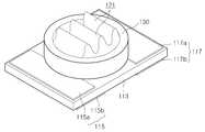
도 1 및 도 2는 일반적인 발광 다이오드 패키지를 보여주는 도면으로서, 도 1 및 도 2에 도시된 바와 같이 일반적인 표면실장형 발광 다이오드 패키지(10)는 베이스판(12)과 상기 베이스판(12) 상에 서로 이격 배치되는 적어도 두 개의 전극(13,14)이 구비된다. 그리고, 발광 다이오드 칩(11)은 전극(13,14)과 와이어(15)로 연결되어 전기적으로 접속된다. 또한, 상기 발광 다이오드 칩(11) 및 와이어(15)를 봉지하는 몰딩부(16)가 형성된다. 이때 상기 몰딩부는 일반적으로 돔(dome) 형상으로 형성된다. 이때 상기 몰딩부를 둘러싸는 케이싱(17)이 더 구비될 수 있다.1 and 2 are views illustrating a general light emitting diode package. As shown in FIGS. 1 and 2, a general surface mount
그리고, 도 3은 일반적인 발광 다이오드 모듈을 보여주는 사시도로서, 도 3에 도시된 바와 같이 발광 다이오드 패키지(10)는 인쇄회로기판(21)에 형성된 회로와 납땜(Soldering)에 의하여 전기적으로 연결되게 설치된다. 이를 발광 다이오드 모듈(20)이라 한다. 이때 발광 다이오드 모듈(20)에는 발광 다이오드 패키지(10)에서 발광되는 광의 지향각을 특정 방향으로 조절하는 렌즈(22)가 부착될 수 있다.3 is a perspective view showing a general light emitting diode module, and as shown in FIG. 3, the light
이 상태에서 스위치가 "ON"상태로 조작되는 경우, 양극으로부터 음극을 통하여 전류가 인가되면서 발광 다이오드 칩(11)이 발광되고, 상기 발광 다이오드 칩(11)으로부터 발광된 광은 렌즈(22)를 통하여 바깥쪽으로 조사되는 방식으로 주변을 밝혀주는 것이다.In this state, when the switch is operated in the "ON" state, the light
이와 같은 발광 다이오드 모듈은 형광등이나 할로겐/백열등 같은 기존의 조명램프에 비하여 상대적으로 오랜 시간 동안 사용할 수 있고, 전력 소모량이 매우 적으며, 밝기가 매우 밝은 것은 물론, 지연시간 없이 순간 점등되고 안전성이 뛰어나며, 다양한 색상으로 연출가능하기 때문에 그 적용범위가 매우 넓어 기존의 전구를 대체할 전구로 자리매김하고 있다.Such a light emitting diode module can be used for a relatively long time compared to a conventional lighting lamp such as a fluorescent lamp or a halogen / incandescent lamp, has a very low power consumption, a very bright brightness, instantaneous lighting without safety, and excellent safety. In addition, since it can be produced in various colors, its application range is very wide, and it is becoming a light bulb to replace a conventional light bulb.
그러나, 이와 같이 이루어지는 종래의 발광 다이오드 모듈에서는 인쇄회로기판(21) 상의 정해진 위치에 발광 다이오드 패키지(10) 및 기타 부품을 실장한 후에 폴리메틸메타크릴레이트(PMMA:Poly methyl methacrylate)재질의 렌즈(21)를 발광 다이오드 패키지(10)에 끼워 넣은 방식으로 설치하거나 실리콘수지로 고정시켜 제작되기 때문에 렌즈(21)의 설치작업시 발광 다이오드 패키지 및 모듈을 손상시킬 우려가 매우 높다는 문제가 있다.However, in the conventional light emitting diode module formed as described above, a lens made of poly methyl methacrylate (PMMA) material after mounting the light
특히, 종래에 조명등에 주로 사용되던 할로겐등, 형광등, 백열등 등과 같은 광원은 전력소모가 많고, 색상 구현에 한계가 있었으며, 수명이 짧기 때문에 유지보수 비용이 많이 소용된다는 단점이 있었다.In particular, light sources such as halogen lamps, fluorescent lamps, incandescent lamps, etc., which are mainly used in the conventional lighting lamps, have a lot of power consumption, have limitations in color implementation, and have a short lifespan.
이에 따라 근래에는 종래에 사용되던 광원을 대체하여 발광 다이오드 장치가 조명등에 적용되는 추세로 빠르게 변하고 있다.Accordingly, in recent years, a light emitting diode device is rapidly changing to a trend of replacing a light source used in the related art.
특히, 조명등은 다양한 형태의 배광(配光) 구조를 요구하고 있으나, 종래의 발광 다이오드 모듈은 설치방향의 수직면에서만 가장 높은 휘도값을 나타내기 때문에 발광된 빛을 다른 방향으로 조사시키고자 하는 경우 별도의 방사각 조절수단이 요구된다는 문제가 있고, 다양한 형태의 배광(配光)을 구현하기 어렵다는 문제가 있다.
In particular, lighting lamps require various types of light distribution structures, but the conventional LED module displays the highest luminance value only in the vertical plane of the installation direction. There is a problem that the radiation angle control means is required, there is a problem that it is difficult to implement various types of light distribution (配 光).
본 발명의 실시형태는 발광 다이오드 칩을 봉지하는 몰딩부 및 발광 다이오드 패키지를 봉지하는 렌즈부를 전통적인 돔(Dome)형상이 아닌 비-돔형상으로 형성하여 설계에 따라 정해지는 방향으로 빛이 분산되어 조사되는 될 수 있는 다양한 배광(配光) 구조를 갖는 발광 다이오드 패키지 및 발광 다이오드 모듈과 이를 이용한 조명등기구를 제공한다.According to the embodiment of the present invention, the molding part encapsulating the light emitting diode chip and the lens part encapsulating the light emitting diode package are formed in a non-dome shape instead of a traditional dome shape so that light is distributed in a direction determined according to the design. Provided are a light emitting diode package and a light emitting diode module having various light distribution structures, and lighting fixtures using the same.
본 발명의 실시형태는 진공밀봉 방식을 이용하여 다양한 배광을 가진 발광 다이오드 패키지 및 모듈을 간편하면서도 신속하게 제작할 수 있는 발광 다이오드 패키지 및 발광 다이오드 모듈의 제조방법을 제공한다.
Embodiments of the present invention provide a method of manufacturing a light emitting diode package and a light emitting diode module that can easily and quickly produce a light emitting diode package and a module having various light distribution using a vacuum sealing method.
본 발명의 일실시예에 따른 발광 다이오드 장치 제조방법은 적어도 하나의 발광 다이오드 칩이 실장된 칩 어셈블리를 마련하는 단계와; 상기 칩 어셈블리를 반전시켜 상부금형에 장착하고 제 1 진공 처리기에 투입시키는 단계와; 제 2 진공 처리기에 하부금형을 투입하고, 하부금형에 형성된 적어도 하나의 수지 충진부에 몰딩 수지를 충진시키는 단계와; 상기 하부금형을 제 1 진공 처리기에 투입시켜 상기 상부금형의 하방에 위치시키는 단계와; 상기 몰딩 수지가 상기 칩 어셈블리의 발광 다이오드 칩를 봉지하도록 상기 상부금형과 하부금형을 결합시키는 단계와; 상기 몰딩 수지를 경화시켜 상기 칩 어셈블리에 비-돔형의 몰딩부를 형성시키는 단계와; 상기 상부 금형 및 하부 금형에서 칩 어셈블리를 분리하는 단계를 포함한다. 특히 상기 칩 어셈블리를 분리하는 단계 이후에는 상기 칩 어셈블리를 적어도 하나 이상의 단위 패키지로 절단하는 다이싱단계를 포함한다.A method of manufacturing a light emitting diode device according to an embodiment of the present invention includes the steps of: providing a chip assembly mounted with at least one LED chip; Inverting the chip assembly, mounting the upper mold to an upper mold, and placing the chip assembly in a first vacuum processor; Injecting a lower mold into the second vacuum processor and filling the molding resin into at least one resin filling portion formed in the lower mold; Injecting the lower mold into a first vacuum processor and placing the lower mold below the upper mold; Coupling the upper mold and the lower mold such that the molding resin encapsulates the light emitting diode chip of the chip assembly; Curing the molding resin to form a non-dom shaped molding in the chip assembly; Separating the chip assembly from the upper mold and the lower mold. In particular, after the step of separating the chip assembly includes a dicing step of cutting the chip assembly into at least one unit package.
그리고, 본 발명의 다른 실시예에 따른 발광 다이오드 장치 제조방법은 적어도 하나의 발광 다이오드 패키지가 실장된 기판 어셈블리를 마련하는 단계와; 상기 기판 어셈블리를 반전시켜 상부금형에 장착하고 제 1 진공 처리기에 투입시키는 단계와; 제 2 진공 처리기에 하부금형을 투입하고, 하부금형에 형성된 적어도 하나의 수지 충진부에 몰딩 수지를 충진시키는 단계와; 상기 하부금형을 제 1 진공 처리기에 투입시켜 상기 상부금형의 하방에 위치시키는 단계와; 상기 몰딩 수지가 상기 기판 어셈블리의 발광 다이오드 패키지를 봉지하도록 상기 상부금형과 하부금형을 결합시키는 단계와; 상기 몰딩 수지를 경화시켜 상기 기판 어셈블리에 비-돔형의 렌즈부를 형성시키는 단계와; 상기 상부 금형 및 하부 금형에서 패키지 어셈블리를 분리하는 단계를 포함한다.In addition, a method of manufacturing a light emitting diode device according to another embodiment of the present invention includes providing a substrate assembly on which at least one light emitting diode package is mounted; Inverting and mounting the substrate assembly to an upper mold and feeding the first vacuum processor into the first vacuum processor; Injecting a lower mold into the second vacuum processor and filling the molding resin into at least one resin filling portion formed in the lower mold; Injecting the lower mold into a first vacuum processor and placing the lower mold below the upper mold; Coupling the upper mold and the lower mold such that the molding resin encapsulates the LED package of the substrate assembly; Curing the molding resin to form a non-dome lens portion in the substrate assembly; Separating the package assembly from the upper mold and the lower mold.
상기 하부금형의 수지 충진부에 몰딩 수지를 충진시키는 단계에서, 상기 하부금형에 형성되는 수지 충진부는 요홈부가 형성되는 비-돔형의 형상을 갖는 것을 특징으로 한다.In the filling of the molding resin into the resin filling portion of the lower mold, the resin filling portion formed in the lower mold is characterized in that it has a non-dome shape in which the groove is formed.
상기 하부금형의 수지 충진부에 몰딩 수지를 충진시키는 단계는 몰딩 수지를 인쇄법 또는 디스펜서법으로 충진시키는 것을 특징으로 한다.The filling of the molding resin into the resin filling part of the lower mold is characterized in that the molding resin is filled by a printing method or a dispenser method.
상기 몰딩 수지는 광투광성 실리콘 수지 또는 에폭시 수지인 것을 특징으로 한다.The molding resin is characterized in that the light transmissive silicone resin or epoxy resin.
본 발명의 일실시예에 따른 발광 다이오드 패키지는 적어도 하나의 발광 다이오드 칩이 실장된 칩 어셈블리와; 상기 발광 다이오드 칩을 봉지하고, 표면에는 광을 분산시키도록 직경방향의 중심선을 따라 소정 너비의 요홈부가 형성되며, 상기 요홈부의 좌우측에는 서로 다른 기울기를 갖는 제 1 투과면과 제 2 투과면이 요홈부를 중심으로 하여 서로 대칭되게 형성되고, 상기 요홈부의 전후 양단부에는 소정의 폭과 기울기를 갖는 제 3 투과면이 경사지게 형성되는 몰딩부를 포함한다. 특히 상기 제 1 투과면은 반원 또는 반타원 형상을 갖고, 제 2 투과면은 중심의 폭이 좁고 중심에서 양측으로 멀어질수록 폭이 넓어지는 형상을 갖는 것을 특징으로 한다.A light emitting diode package according to an embodiment of the present invention includes a chip assembly mounted with at least one light emitting diode chip; The light emitting diode chip is encapsulated, and grooves having a predetermined width are formed along a center line in a radial direction to disperse light on the surface, and the first transmission surface and the second transmission surface having different inclinations are formed on left and right sides of the groove portion. It is formed symmetrically with respect to the center portion, the front and rear ends of the groove portion includes a molding portion in which the third transmission surface having a predetermined width and inclination is formed to be inclined. In particular, the first transmission surface has a semi-circular or semi-elliptic shape, and the second transmission surface has a shape in which the width of the center is narrow and wider as the distance from the center to both sides is wider.
본 발명의 다른 실시예에 따른 발광 다이오드 패키지는 적어도 하나의 발광 다이오드 칩이 실장된 칩 어셈블리와; 상기 발광 다이오드 칩을 봉지하고, 표면에는 광을 분산시키도록 직경방향으로 형성되는 요홈부가 소정 간격으로 다수개 구비되어 물결무늬를 형성하는 것을 특징으로 한다.According to another embodiment of the present invention, a light emitting diode package includes: a chip assembly having at least one light emitting diode chip mounted thereon; The light emitting diode chip is encapsulated, and a plurality of groove portions formed in a radial direction so as to disperse light are provided at predetermined intervals to form a wave pattern.
상기 칩 어셈블리는 베이스판과; 상기 베이스판에 서로 이격 배치되는 적어도 두 개의 전극을 포함하고, 상기 발광 다이오드 칩이 상기 전극에 전기적으로 연결되는 것을 특징으로 한다.The chip assembly includes a base plate; At least two electrodes spaced apart from each other on the base plate, characterized in that the light emitting diode chip is electrically connected to the electrode.
본 발명의 일실시예에 따른 발광 다이오드 모듈은 적어도 하나의 발광 다이오드 패키지가 실장된 기판 어셈블리와; 상기 발광 다이오드 패키지를 봉지하고, 표면에 광을 분산시키도록 적어도 하나 이상의 요홈부가 형성되며, 요홈부의 가장자리 중 적어도 한 지점에는 요홈부의 다른 가장자리보다 높이가 낮은 개구부가 형성되는 렌즈부를 포함한다.According to an embodiment of the present invention, a light emitting diode module includes: a substrate assembly having at least one light emitting diode package mounted thereon; At least one recess is formed to encapsulate the light emitting diode package and to disperse light on the surface, and at least one of the edges of the recess includes a lens portion having an opening having a lower height than other edges of the recess.
상기 기판 어셈블리는 소정의 전극 패턴에 형성된 인쇄회로기판을 포함하고, 상기 발광 다이오드 패키지가 상기 전극 패턴에 전기적으로 연결되는 것을 특징으로 한다.
The substrate assembly may include a printed circuit board formed on a predetermined electrode pattern, and the light emitting diode package may be electrically connected to the electrode pattern.
본 발명의 실시예에 따르면, 발광 다이오드 칩을 봉지하는 몰딩부 및 발광 다이오드 패키지를 봉지하는 렌즈부를 전통적인 돔(Dome)형상이 아니라 비-돔형태로 제작하여 다양한 배광(配光) 구조를 갖도록 형성되기 때문에 발광 다이오드 칩으로부터 발생된 빛이 설계에 따라 정해지는 방향으로 분산되어 조사(照射)될 수 있다.According to an embodiment of the present invention, the molding part encapsulating the light emitting diode chip and the lens part encapsulating the light emitting diode package are manufactured in a non-dome shape instead of a traditional dome shape to form various light distribution structures. Therefore, the light generated from the light emitting diode chip can be distributed and irradiated in a direction determined according to the design.
이에 따라 소비자가 원하는 배광 구조를 갖는 다양한 형태의 발광 다이오드 모듈 및 조명등기구를 제공할 수 있다.Accordingly, it is possible to provide various types of light emitting diode modules and lighting fixtures having a light distribution structure desired by the consumer.
또한, 정해진 형상을 갖는 금형을 이용한 진공밀봉 방식으로 비-돔형의 몰딩부 또는 렌즈부를 형성하기 때문에 별도로 몰딩부 및 렌즈부를 형성하는 몰딩 수지에 포함된 기포를 제거하는 공정 및 렌즈를 장착하는 공정을 적용하지 않아도 됨에 따라 간편하면서도 신속하게 발광 다이오드 패키지 및 모듈을 제작할 수 있어 그 생산비를 절감하고 생산수율을 향상시킬 수 있다.
In addition, since the non-dom shaped molding part or the lens part is formed by a vacuum sealing method using a mold having a predetermined shape, a process of removing bubbles contained in the molding resin forming the molding part and the lens part separately and a process of mounting the lens are provided. As there is no application, it is possible to manufacture LED packages and modules easily and quickly, thereby reducing the production cost and improving the production yield.
도 1은 일반적인 발광 다이오드 패키지를 보여주는 단면도이고,
도 2는 일반적인 발광 다이오드 패키지를 보여주는 사시도이며,
도 3은 일반적인 발광 다이오드 모듈을 보여주는 사시도이고,
도 4는 본 발명의 일실시예에 따른 발광 다이오드 패키지를 보여주는 단면도이며,
도 5는 본 발명의 일실시예에 따른 발광 다이오드 패키지를 보여주는 사시도이고,
도 6은 본 발명의 다른 실시예에 따른 발광 다이오드 패키지를 보여주는 사시도이며,
도 7은 본 발명의 일실시예에 따른 발광 다이오드 모듈을 보여주는 사시도이고,
도 8a 내지 도 8h는 본 발명의 일실시예에 따른 발광 다이오드 패키지를 제조하는 방법을 보여주는 도면이며,
도 9a 내지 도 9d는 본 발명의 일실시예에 따른 발광 다이오드 모듈을 제조하는 방법을 보여주는 도면이고,
도 10a는 종래의 발광 다이오드 패키지에 대한 광 지향각을 알아본 실험결과이며,
도 10b는 본 발명의 일실시예에 따른 발광 다이오드 패키지에 대한 광 지향각을 알아본 실험결과이다.1 is a cross-sectional view showing a typical light emitting diode package,
2 is a perspective view showing a typical light emitting diode package,
3 is a perspective view showing a general light emitting diode module,
4 is a cross-sectional view showing a light emitting diode package according to an embodiment of the present invention.
5 is a perspective view showing a light emitting diode package according to an embodiment of the present invention;
6 is a perspective view showing a light emitting diode package according to another embodiment of the present invention,
7 is a perspective view showing a light emitting diode module according to an embodiment of the present invention;
8A to 8H are views illustrating a method of manufacturing a light emitting diode package according to an embodiment of the present invention.
9A to 9D are views illustrating a method of manufacturing a light emitting diode module according to an embodiment of the present invention.
10A is an experimental result of finding a light directivity angle for a conventional LED package,
10B is an experimental result of finding a light directivity angle for the LED package according to the embodiment of the present invention.
이하, 첨부된 도면을 참조하여 본 발명의 실시예를 더욱 상세히 설명하기로 한다. 그러나 본 발명은 이하에서 개시되는 실시예에 한정되는 것이 아니라 서로 다른 다양한 형태로 구현될 것이며, 단지 본 실시예들은 본 발명의 개시가 완전하도록 하며, 통상의 지식을 가진 자에게 발명의 범주를 완전하게 알려주기 위해 제공되는 것이다. 도면상에서 동일 부호는 동일한 요소를 지칭한다.Hereinafter, with reference to the accompanying drawings will be described an embodiment of the present invention in more detail. It will be apparent to those skilled in the art that the present invention may be embodied in many different forms and should not be construed as limited to the embodiments set forth herein. Rather, these embodiments are provided so that this disclosure will be thorough and complete, It is provided to let you know. Like numbers refer to like elements in the figures.
본 발명의 설명에서 발광 다이오드 장치는 발광 다이오드 패키지 및 발광 다이오드 모듈을 모두 포함하는 의미로 사용하였다.
In the description of the present invention, the light emitting diode device is used to include both the light emitting diode package and the light emitting diode module.
도 4는 본 발명의 일실시예에 따른 발광 다이오드 패키지를 보여주는 단면도이고, 도 5는 본 발명의 일실시예에 따른 발광 다이오드 패키지를 보여주는 사시도이며, 도 6은 본 발명의 다른 실시예에 따른 발광 다이오드 패키지를 보여주는 사시도이다.Figure 4 is a cross-sectional view showing a light emitting diode package according to an embodiment of the present invention, Figure 5 is a perspective view showing a light emitting diode package according to an embodiment of the present invention, Figure 6 is a light emitting according to another embodiment of the present invention A perspective view showing a diode package.
도 4 및 도 5에 도시된 바와 같이 본 발명의 일실예에 따른 발광 다이오드 패키지는 적어도 하나의 발광 다이오드 칩(111)이 실장된 칩 어셈블리(110)와; 상기 발광 다이오드 칩(111)을 봉지하고, 표면에 광을 분산시키는 적어도 하나 이상의 요홈부(121)가 형성되는 몰딩부(120)를 포함한다.As shown in FIGS. 4 and 5, a light emitting diode package according to an embodiment of the present invention includes a
칩 어셈블리(110)는 베이스판(113)과, 상기 베이스판(113)에서 서로 이격 배치되도록 상기 베이스판(113)의 일 단에 형성된 제 1 전극(115) 및 상기 베이스판(113)의 타 단에 상기 제 1 전극(115)과 소정 간격 이격되어 형성된 제 2 전극(117)을 포함한다.The
상기 제 1 전극(115)은 상기 베이스판(113)의 상부 즉, 발광 다이오드 칩(111)이 실장되는 부분에 형성되는 상부면(115a)과, 상기 베이스판(113)의 하부에 형성되는 하부면(115b)을 포함한다. 또한, 상기 제 2 전극(117) 역시 상기 베이스판(113)의 상부 즉, 발광 다이오드 칩(111)이 실장되는 부분에 형성되는 상부면(117a)과, 상기 베이스판(113)의 하부에 형성되는 하부면(117b)을 포함한다. 이때 상기 제 1 전극(115) 및 제 2 전극(117)의 상부면(115a,117a) 및 하부면(115b,117b)은 상기 베이스판(113)를 관통하여 형성되는 비아홀에 형성된 연결부(115c,117c)를 통하여 연결된다. 그리고, 상기 제 1 전극(115)의 상부면(115a) 및 제 2 전극(117)의 상부면(117a)은 상기 발광 다이오드 칩(111)으로부터 조사되는 광의 반사효율을 높이기 위하여, 반사효율이 높은 재료 예를 들면, 은(Ag)을 포함할 수 있다. 또한, 상기 제 1 전극(115)의 하부면(115b) 및 제 2 전극(117)의 하부면(117b)은 납땜으로 솔더링되는 부분으로서, 납땜성을 좋게 하기 위하여, 금(Au) 또는 주석(Sn)을 포함하여 형성할 수 있다. 상기 제 1 전극(115) 및 제 2 전극(117)은 전술된 구성에 한정되지 않고, 제 1 전극(115) 및 제 2 전극(117)의 상부면(115a,117a) 및 하부면(115b,117b)을 연결할 수 있으면 어떠한 방식으로도 변경되어 구현될 수 있다. 예를 들어 제 1 전극(115) 및 제 2 전극(117)의 상부면(115a,117a) 및 하부면(115b,117b)은 베이스판(113)에 비아홀을 형성하지 않고, 베이스판(113)의 외주면을 따라 연결부를 형성할 수 있을 것이다.The
상기 발광 다이오드 칩(111)은 상기 제 1 전극(115)의 상부면(115a) 또는 베이스판(113)의 상면에 구비되며, 상기 와이어(119)를 통하여 상기 제 1 전극(115)의 상부면(115a) 및 제 2 전극(117)의 상부면(117a)에 연결된다. 한편, 상기 발광 다이오드 칩(111)은 상기 제 1 전극(115)의 상부면(115a) 상에 실장되며, 상기 와이어(119)를 통하여 상기 제 2 전극(117)의 상부면(117a)에 연결될 수 있다.The light emitting
몰딩부(120)는 상기 발광 다이오드 칩(111) 및 와이어(119)를 봉지하여 보호하는 수단으로서, 상기 베이스판(113)의 상면에 형성된다. 이때 상기 몰딩부(120)의 표면에는 발광 다이오드 칩(111)에서 발광되는 광의 지향각을 조절 또는 분산하기 위하여 적어도 하나 이상의 요홈부(121)가 형성된다. 상기 요홈부(121) 및 요홈부(121)를 포함하는 몰딩부(120)의 표면 형상은 광의 지향각을 조절 또는 분산하기 위하여 다양하게 설계하여 구현할 수 있다. 예를 들어 본 실시예에서는 몰딩부(120) 직경방향의 중심선을 따라 소정 너비의 요홈부(121)가 형성되고, 상기 요홈부(121)의 좌우측에는 서로 다른 기울기를 갖는 제 1 투과면(122)과 제 2 투과면(123)이 요홈부(121)를 중심으로 하여 서로 대칭되게 형성되며, 상기 요홈부(121)의 전후 양단부에는 소정의 폭과 기울기를 갖는 제 3 투과면(124)이 경사지게 형성된다. 이때 상기 제 1 투과면(122)은 대략 반원 또는 반타원 형상을 갖고 제 2 투과면(123)은 중심의 폭이 좁고 중심에서 양측으로 멀어질수록 폭이 넓어지는 형상을 갖는다. 특히 제 1 투과면(122)과 제 2 투과면(123)은 서로 반대의 기울기를 갖는 것이 바람직하다.The
또한, 도 6에 도시된 바와 같이 상기 몰딩부(130)는 다른 실시예로 직경방향으로 형성되는 요홈부(131)가 소정 간격으로 다수개 구비되어 물결무늬를 형성할 수 있다.In addition, as shown in FIG. 6, the
이와 같이 몰딩부(120,130)의 형상을 종래의 돔형이 아닌 비-돔형, 정확하게는 요홈부(121,131)를 갖는 비-돔형으로 형성함에 따라 발광 다이오드 칩(111)에서 발생된 광이 일방향으로 집중되지 않고, 분산되어 소비자가 원하는 다양한 배광(配光) 구조를 형성할 수 있는 것이다.As such, the shape of the
이때 상기 몰딩부(120,130)를 형성하는 몰딩수지는 비교적 경도가 높고, 투명한 실리콘 수지 또는 에폭시 수지로 형성할 수 있다. 하지만 이에 한정되지 않고, 발광 다이오드 패키지(100)의 용도에 따라 광이 투과될 수 있을 정도로 투명한 수지이고, 진공밀봉 방식으로 베이스판(113)에 형성될 수 있다면 어떠한 재료가 사용되어도 무방할 것이다. 또한, 상기 발광 다이오드 칩(111)에서 방출된 광의 파장을 전환시켜 다양한 색상을 구현하기 위하여 다양한 종류의 형광체(미도시)가 혼합될 수 있다.In this case, the molding resin forming the
상기 몰딩부(120,130)의 주변에는 상기 몰딩부(120,130)의 형성을 가이드 하는 케이싱(118)이 더 형성될 수 있다.A
상기 케이싱(118)은 상기 베이스판(113)의 상면에 형성되어 상기 몰딩부(120,130)가 원활하게 비-돔형상을 유지할 수 있도록 몰딩부(120,130)의 외각을 둘러싸는 형상을 갖는다. 물론 케이싱(118)은 이에 한정되지 않고 상기 몰딩부(120,130)의 형상에 따라 다양하게 변경되어 구현될 수 있다.
The
다음으로, 도 7을 참조하여 본 발명의 일실시예에 따른 발광 다이오드 모듈을 설명한다.Next, a light emitting diode module according to an embodiment of the present invention will be described with reference to FIG. 7.
도 7에 도시된 바와 같이 본 발명의 일실시예에 따른 발광 다이오드 모듈(200)은 적어도 하나의 발광 다이오드 패키지(100)가 실장된 기판 어셈블리(210)와, 상기 발광 다이오드 패키지(100)를 봉지하고, 표면에 광을 분산시키는 적어도 하나 이상의 요홈부(221)가 형성되는 렌즈부(220)를 포함한다.As shown in FIG. 7, the
발광 다이오드 패키지(100)는 전술된 발광 다이오드 패키지(100)를 그대로 사용하여도 무방하다. 이에 따라 중복되는 설명은 생략하기로 한다. 다만, 발광 다이오드 패키지(100)의 몰딩부(120) 형상은 전술된 실시예에서 제시된 요홈부(221)를 갖는 비-돔형상에 제한되지 않고, 종래의 돔형 형상을 가져도 무방하다.The light emitting
기판 어셈블리(210)는 상기 발광 다이오드 패키지(100)를 전기적으로 연결하기 위한 소정의 전극 패턴이 형성되는 인쇄회로기판(211)을 포함한다. 그래서 상기 발광 다이오드 패키지(100)가 상기 인쇄회로기판(211)에 실장되어 외부로부터 전원을 인가받을 수 있도록 연결된다.The
렌즈부(220)는 상기 발광 다이오드 패키지(100)에서 발생되는 광의 지향각을 조절 또는 분산시키는 수단을 갖고, 본 실시예에서는 발광 다이오드 패키지(100)를 봉지하여 보호하는 수단을 더 갖는다. 이때 상기 렌즈부(220)의 표면에는 발광 다이오드 패키지(100)에서 발광되는 광의 지향각을 조절 또는 분산하기 위하여 적어도 하나 이상의 요홈부(221)가 형성된다. 예를 들어 원형의 요홈부(221)를 갖고 요홈부(221)의 중심에는 돌출부(223)가 형성되며, 요홈부(221)의 가장자리 중 적어도 한 지점에는 요홈부(221)의 다른 가장자리보다 높이가 낮은 개구부(225)가 형성된다. 그래서, 발광 다이오드 패키지(100)에서 발광되는 광의 지향을 효과적으로 분산시킨다. 물론 상기 렌즈부의 형상은 이에 한정되지 않고, 상기 렌즈부(220)는 전술된 실시예의 몰딩부(120)와 같이 상기 요홈부(221) 및 요홈부(221)를 포함하는 렌즈부의 표면 형상을 광의 지향각이 조절 또는 분산되도록 다양하게 설계하여 구현할 수 있다. 그리고, 상기 렌즈부(220)를 형성하는 몰딩수지는 비교적 경도가 높고, 투명 또는 반투명한 실리콘 수지 또는 에폭시 수지로 형성할 수 있다. 하지만 이에 한정되지 않고, 발광 다이오드 모듈(200)의 용도에 따라 광이 투과될 수 있을 정도로 투명한 수지이고, 진공밀봉 방식으로 인쇄회로기판(211)에 형성될 수 있다면 어떠한 재료가 사용되어도 무방할 것이다. 또한, 상기 발광 다이오드 패키지(100)에서 방출된 광의 파장을 전환시켜 다양한 색상을 구현하기 위하여 다양한 종류의 형광체(미도시)가 혼합될 수 있다.
The
다음으로 도 8a 내지 도 8h를 참조하여 본 발명의 일실시예에 따른 발광 다이오드 패키지의 제조방법을 설명한다.Next, a method of manufacturing a light emitting diode package according to an embodiment of the present invention will be described with reference to FIGS. 8A to 8H.
도 8a 내지 도 8i는 본 발명의 일실시예에 따른 발광 다이오드 패키지를 제조하는 방법을 보여주는 도면이고, 도면에 도시된 바와 같이 본 발명의 일실시예에 따른 발광 다이오드 패키지의 제조 방법은 다음과 같다.8A to 8I are views illustrating a method of manufacturing a light emitting diode package according to an embodiment of the present invention, and as shown in the drawing, a method of manufacturing a light emitting diode package according to an embodiment of the present invention is as follows. .
먼저, 본 발명의 일실시예에 따른 발광 다이오드 패키지를 진공밀봉 방식에 의해 제조하기 위한 설비를 설명한다. 본 실시예에서는 진공밀봉 방식 중 몰딩수지를 인쇄법에 의해 공급하는 방식을 예로 하여 설명하도록 한다.First, an apparatus for manufacturing a light emitting diode package according to an embodiment of the present invention by a vacuum sealing method will be described. In this embodiment, a method of supplying a molding resin by a printing method of the vacuum sealing method will be described as an example.
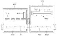
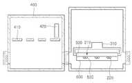
진공밀봉 설비는 적어도 2개의 진공 처리기(300,400)를 포함한다. 그래서, 제 1 진공 처리기(300)에서는 칩 어셈블리(110)가 고정되는 상부금형(500)과 몰딩수지(120a)가 충진된 하부금형(600)을 결합시키고, 제 2 진공 처리기(400)에서는 하부금형(600)에 몰딩수지(120a)를 충진하는 공정이 이루어진다. 이에 따라 하부금형(600)에는 몰딩수지(120a)가 충진되는 요홈부(121)가 형성되는 비-돔형의 형상을 갖는 수지 충진부(610)가 형성된다. 그리고, 제 2 진공 처리기(400)에는 상기 수지 충진부(610)와 대응되는 소정의 패턴이 형성된 마스크(410) 및 몰딩수지(120a)를 상기 마스크(410)의 패턴으로 일정하게 주입시키기 위한 스퀴지(420)가 구비된다. 그리고, 제 1 진공 처리기(300)에는 칩 어셈블리(110)를 고정시키는 상부금형(500)을 취부하여 이송시키는 아암(310)이 구비된다. 상기 제 1 진공 처리기(300) 및 제 2 진공 처리기(400)는 외부와 내부를 격리시키는 함체와 같은 수단으로서, 내부를 진공환경으로 조성할 수 있는 수단이라면 어떠한 수단이 사용되어도 무방하다.The vacuum seal facility includes at least two vacuum processors 300,400. Thus, in the
전술된 진공밀봉 설비를 이용하여 발광 다이오드 패키지를 제조하기 위하여 먼저, 칩 어셈블리(110)를 마련한다. 칩 어셈블리(110)는 적어도 하나의 발광 다이오드 칩을 베이스판에 실장하여 마련한다. 이렇게 마련된 칩 어셈블리는 도 8a에 도시된 바와 같이 상부금형(500)에 고정시킨 다음 제 1 진공 처리기(300)의 아암(310)으로 취부한다.In order to manufacture a light emitting diode package using the above-mentioned vacuum sealing facility, first, a
그리고 도 8b에 도시된 바와 같이 제 2 진공 처리기(400)에 하부금형(600)을 투입한 다음 하부금형(600)의 수지 충진부(610)에 몰딩수지(120a)를 충진한다. 본 실시예에서는 인쇄법을 이용하여 몰딩수지(120a)를 충진하였다. 이에 따라 하부금형(600)의 상부에 마스크(410)를 접근시키고, 마스크(410)의 상면에서 스퀴지(420)를 이용하여 몰딩수지(120a)를 하부금형(600)의 수지 충진부(610)에 충진시킨다. 물론 수지 충진부(610)에 몰딩수지(120a)를 충진하는 방법은 인쇄법에 한정되지 않고, 제 2 진공 처리기(400) 내에서 수지 충진부(610)에 몰딩수지(120a)를 충진할 수 있는 다양한 방법이 적용될 수 있다. 예를 들어 디스펜서를 이용하여 수지 충진부에 몰딩수지를 충진하는 디스펜서법을 사용할 수도 있다.As shown in FIG. 8B, the
그런 다음, 도 8c에 도시된 바와 같이 제 2 진공 처리기(400)가 진공상태로 감압된 상태에서 하부금형(600)을 제 2 진공 처리기(400)에 소정 시간동안 유지시킨다. 그러면, 제 2 진공 처리기(400) 내부와 몰딩수지(120a) 내부의 압력차에 의해 몰딩수지(120a)에 포함된 기포가 몰딩수지(120a) 내부에서 외부로 배출된다. 따라서 몰딩수지(120a)에서 기포를 제거하기 위한 별도의 공정을 생략할 수 있다.Then, as shown in FIG. 8C, the
이렇게 하부금형(600)의 수지 충진부(610)에 몰딩수지(120a)가 충진되었다면 도 8d에 도시된 바와 같이 하부금형(600)을 제 1 진공 처리기(300)로 이송시킨다.When the
그리고, 도 8e에 도시된 바와 같이 상기 하부금형(600)을 제 1 진공 처리기(300)에 투입시켜 상기 상부금형(500)의 하방에 위치시킨다.As shown in FIG. 8E, the
그런 다음, 아암(310)을 하강시켜 칩 어셈블리(110)가 고정된 상부금형(500)을 하부금형(600)에 결합시킨다. 그러면, 하부금형(600)의 수지 충진부(610)에 충진된 몰딩수지(120a)에 의해 상기 칩 어셈블리(110)의 발광 다이오드 칩(111)이 봉지된다.Then, the
그리고, 하부금형(600)과 상부금형(500)이 결합된 상태에서 소정 시간, 바람직하게는 몰딩수지(120a)가 충분히 경화되는 시간을 경과시켜 상기 칩 어셈블리(110)에 비-돔형의 몰딩부(120)를 형성시킨다. 이때 형성되는 몰딩부(120)의 형상은 하부금형(600)에 형성된 수지 충진부(610)의 형상에 의해 결정된다. 몰딩부(120)의 경화는 상온에서 진행할 수 있지만 이에 한정되지 않고, 도 8f에 도시된 바와 같이 소정의 온도로 가열되는 별도의 건조기(700)에 하부금형(600)과 상부금형(500)이 결합된 상태로 투입하여 몰딩부(120)의 경화가 바람직하게 이루어지도록 할 수 있다.In addition, a predetermined time, preferably a time that the
이렇게 몰딩부(120)의 경화가 충분히 이루어졌다면 도 8g에 도시된 바와 같이 상부금형(500) 및 하부금형(600)에서 몰딩부(120)가 형성된 칩 어셈블리(110)를 분리시킨다.When the curing of the
그리고, 몰딩부(120)가 형성된 칩 어셈블리(110)는 도 8h에 도시된 바와 같이 적어도 하나 이상의 단위 발광 다이오드 패키지(100)로 절단하는 다이싱단계를 더 포함할 수 있다.In addition, the
상기와 같이 진공밀봉 방식 및 몰드프레스 방식에 의해 특정 형상을 갖는 몰딩부(120)를 간편하면서도 신속하게 제작할 수 있다.
As described above, the
다음으로 본 발명의 일실시예에 따른 발광 다이오드 모듈의 제조방법에 대하여 도면을 참조하여 설명한다.Next, a method of manufacturing a light emitting diode module according to an embodiment of the present invention will be described with reference to the drawings.
도 9a 내지 도 9d는 본 발명의 일실시예에 따른 발광 다이오드 모듈을 제조하는 방법을 보여주는 도면이다.9A to 9D are views illustrating a method of manufacturing a light emitting diode module according to an embodiment of the present invention.
발광 다이오드 모듈의 제조방법은 전술된 발광 다이오드 패키지의 제조방법에 사용된 진공밀봉 방식 및 몰드프레스 방식이 유사하게 적용된다. 이에 따라 중복되는 설명은 생략 또는 간소화하여 설명하기로 한다. 다만, 발광 다이오드 패키지(100)의 몰딩부(120) 형상은 전술된 실시예에서 제시된 요홈부(121)를 갖는 비-돔형상에 제한되지 않고, 종래의 돔형 형상을 가져도 무방하다.The manufacturing method of the LED module is similarly applied to the vacuum sealing method and the mold press method used in the above-described method of manufacturing the LED package. Accordingly, duplicate description will be omitted or simplified. However, the shape of the
본 발명의 일실시예에 따른 발광 다이오드 모듈의 제조방법은 먼저, 도 9a에 도시된 바와 같이 적어도 하나의 발광 다이오드 패키지(100)가 실장된 기판 어셈블리(210)를 마련한 다음, 상기 기판 어셈블리(210)를 반전시켜 상부금형(500)에 장착하고 제 1 진공 처리기(300)에 마련된 아암(310)에 취부시킨다. 이때 기판 어셈블리(210)에 실징된 발광 다이오드 패키지(100)는 돔형의 몰딩부(120)가 형성된 것을 사용한다. 물론 이에 한정되지 않고, 사용자의 의도에 따라 다양으로 형성된 몰딩부(120)가 적용될 수 있다.In the method of manufacturing a light emitting diode module according to an embodiment of the present invention, first, as shown in FIG. 9A, a
그리고, 제 2 진공 처리기(400)에 하부금형(600)을 투입하고, 하부금형(600)에 형성된 적어도 하나의 수지 충진부(610)에 몰딩수지(220a)를 충진시킨다. 이때 몰딩수지(220a)의 충진은 인쇄법 또는 디스펜서법이 사용될 수 있다.Then, the
그런 다음, 도 9b에 도시된 바와 같이 상기 하부금형(600)을 제 1 진공 처리기(300)에 투입시켜 상기 상부금형(500)의 하방에 위치시키고, 상기 몰딩수지(220a)가 상기 기판 어셈블리(210)의 발광 다이오드 패키지(100)를 봉지하도록 상기 상부금형(500)과 하부금형(600)을 결합시킨다. 그러면, 하부금형(600)의 수지 충진부(610)에 충진된 몰딩수지(220a)에 의해 상기 기판 어셈블리(210)의 발광 다이오드 패키지(100)가 봉지된다.Next, as shown in FIG. 9B, the
그리고, 하부금형(600)과 상부금형(500)이 결합된 상태에서 소정 시간, 바람직하게는 몰딩수지(220a)가 충분히 경화되는 시간을 경과시켜 상기 기판 어셈블리(210)에 비-돔형의 렌즈부(220)를 형성시킨다. 이때 형성되는 렌즈부(220)의 형상은 하부금형(600)에 형성된 수지 충진부(610)의 형상에 의해 결정된다. 렌즈부(220)의 경화는 상온에서 진행할 수 있지만 이에 한정되지 않고, 도 9c에 도시된 바와 같이 소정의 온도로 가열되는 별도의 건조기(700)에 하부금형(600)과 상부금형(500)을 결합한 상태로 투입하여 렌즈부(220)의 경화가 바람직하게 이루어지도록 할 수 있다.In addition, a predetermined time, preferably a time when the
이렇게 렌즈부(220)의 경화가 충분히 이루어졌다면 도 9d에 도시된 바와 같이 상부금형(500) 및 하부금형(600)에서 렌즈부(220)가 형성된 기판 어셈블리(210)를 분리시켜 발광 다이오드 모듈(200)을 완성시킨다.
When the curing of the
다음으로 종래의 발광 다이오드 패키지과 본 발명의 일실시예에 따른 발광 다이오드 패키지의 광 지향각을 비교하여 본 발명의 일실시에에 따른 발광 다이오드 패키지의 광 지향각 조절 효과를 알아본다.Next, the light directing angle of the light emitting diode package according to the exemplary embodiment of the present invention is compared by comparing the light directing angle of the conventional LED package and the light emitting diode package according to the exemplary embodiment of the present invention.
도 10a는 종래의 발광 다이오드 패키지에 대한 광 지향각을 알아본 실험결과이고, 도 10b는 본 발명의 일실시예에 따른 발광 다이오드 패키지에 대한 광 지향각을 알아본 실험결과이다.FIG. 10A is an experimental result of finding a light directivity angle with respect to a conventional LED package, and FIG. 10B is a test result of finding a light directivity angle with respect to the LED package according to an embodiment of the present invention.
도 10a에서 알 수 있듯이 종래의 돔형 몰딩부를 갖는 발광 다이오드 패키지는 일정한 광 지향각으로 균일하게 광이 조사되고 있는 것을 알 수 있고, 도 10b에서 알 수 있듯이 본 발명의 일실시예에 따른 비-돔형 몰딩부를 갖는 발광 다이오드 패키지는 광을 분산하여 사용자가 원하는 광 지향으로 원하는 만큼 광이 조사되고 있는 것을 알 수 있다. 따라서, 비-돔형 몰딩부의 표면 형상을 변형하여 사용자가 원하는 광 지향각을 구현할 수 있음을 알 수 있었다.
As can be seen in FIG. 10A, a light emitting diode package having a conventional domed molding part is uniformly irradiated with a constant light directing angle, and as shown in FIG. 10B, a non-dome type according to an embodiment of the present invention. It can be seen that the LED package having a molding part is irradiated with light as much as desired by the user by dispersing light and desired light direction. Therefore, it can be seen that the shape of the non-dome-shaped molding part can be modified to implement a desired light directing angle.
전술된 바와 같이 제조되는 발광 다이오드 패키지 및 발광 다이오드 모듈은 각각 패키지 및 모듈 단위로 제조되어 다양한 분야에 적용되어 사용된다. 예를 들어 본 발명에 따라 제조되는 비-돔형의 몰딩부가 형성된 발광 다이오드 패키지는 적어도 하나 이상이 인쇄회로기판에 실장되어 발광 다이오드 모듈을 구성하고, 이렇게 구성된 발광 다이오드 모듈은 적어도 하나 이상 배열되어 조명등기구의 광원으로 사용된다. 또한, 본 발명에 따라 제조되는 비-돔형의 렌즈부가 형성된 발광 다이오드 모듈은 적어도 하나 이상 배열되어 조명등기구의 광원으로 사용된다.The light emitting diode package and the light emitting diode module manufactured as described above are manufactured in package and module units, respectively, and applied to various fields. For example, a light emitting diode package having a non-dom shaped molding part manufactured according to the present invention may be mounted on a printed circuit board to form a light emitting diode module. It is used as a light source. In addition, at least one light emitting diode module having a non-dome lens part manufactured according to the present invention is arranged and used as a light source of a lighting fixture.
본 발명에 예시된 발광 다이오드 패키지 및 발광 다이오드 모듈은 표면실장형 패키징에 의해 제조되는 것을 예로 하여 설명하였지만, 이에 한정되지 않고 비-돔형의 몰딩부 및 렌즈부가 형성된다면 어떠한 타입의 패키징에라도 적용이 가능할 것이다. 예를 들어 램프형 발광 다이오드 패키징에도 적용이 가능할 것이다.Although the light emitting diode package and the light emitting diode module illustrated in the present invention have been described as an example of being manufactured by surface-mounted packaging, the present invention is not limited thereto. will be. For example, it may be applied to lamp type LED packaging.
이상에서는 도면 및 실시예를 참조하여 설명하였지만, 해당 기술 분야의 숙련된 당업자는 하기의 특허청구범위에 기재된 본 발명의 기술적 사상으로부터 벗어나지 않는 범위 내에서 본 발명을 다양하게 수정 및 변경시킬 수 있음을 이해할 수 있을 것이다.
Although described above with reference to the drawings and embodiments, those skilled in the art can be variously modified and changed within the scope of the invention without departing from the spirit of the invention described in the claims below. I can understand.
100: 발광 다이오드 패키지110: 칩 어셈블리
111: 발광 다이오드 칩113: 베이스판
115,117: 전극118: 케이싱
119: 와이어120: 몰딩부
121: 요홈부200: 발광 다이오드 모듈
210: 기판 어셈블리211: 인쇄회로기판
220: 렌즈부221: 요홈부100: light emitting diode package 110: chip assembly
111: LED chip 113: base plate
115,117: electrode 118: casing
119: wire 120: molding part
121: groove 200: light emitting diode module
210: substrate assembly 211: printed circuit board
220: lens portion 221: groove portion
Claims (14)
Translated fromKorean상기 칩 어셈블리를 반전시켜 상부금형에 장착하고 제 1 진공 처리기에 투입시키는 단계와;
제 2 진공 처리기에 하부금형을 투입하고, 하부금형에 형성된 적어도 하나의 수지 충진부에 몰딩 수지를 충진시키는 단계와;
상기 하부금형을 제 1 진공 처리기에 투입시켜 상기 상부금형의 하방에 위치시키는 단계와;
상기 몰딩 수지가 상기 칩 어셈블리의 발광 다이오드 칩를 봉지하도록 상기 상부금형과 하부금형을 결합시키는 단계와;
상기 몰딩 수지를 경화시켜 상기 칩 어셈블리에 비-돔형의 몰딩부를 형성시키는 단계와;
상기 상부 금형 및 하부 금형에서 칩 어셈블리를 분리하는 단계를 포함하는 발광 다이오드 장치 제조방법.
Providing a chip assembly mounted with at least one light emitting diode chip;
Inverting the chip assembly, mounting the upper mold to an upper mold, and placing the chip assembly in a first vacuum processor;
Injecting a lower mold into the second vacuum processor and filling the molding resin into at least one resin filling portion formed in the lower mold;
Injecting the lower mold into a first vacuum processor and placing the lower mold below the upper mold;
Coupling the upper mold and the lower mold such that the molding resin encapsulates the light emitting diode chip of the chip assembly;
Curing the molding resin to form a non-dom shaped molding in the chip assembly;
And separating the chip assembly from the upper mold and the lower mold.
상기 칩 어셈블리를 분리하는 단계 이후에는
상기 칩 어셈블리를 적어도 하나 이상의 단위 패키지로 절단하는 다이싱단계를 포함하는 발광 다이오드 장치 제조방법.
The method according to claim 1,
After removing the chip assembly
And dicing the chip assembly into at least one unit package.
상기 기판 어셈블리를 반전시켜 상부금형에 장착하고 제 1 진공 처리기에 투입시키는 단계와;
제 2 진공 처리기에 하부금형을 투입하고, 하부금형에 형성된 적어도 하나의 수지 충진부에 몰딩 수지를 충진시키는 단계와;
상기 하부금형을 제 1 진공 처리기에 투입시켜 상기 상부금형의 하방에 위치시키는 단계와;
상기 몰딩 수지가 상기 기판 어셈블리의 발광 다이오드 패키지를 봉지하도록 상기 상부금형과 하부금형을 결합시키는 단계와;
상기 몰딩 수지를 경화시켜 상기 기판 어셈블리에 비-돔형의 렌즈부를 형성시키는 단계와;
상기 상부 금형 및 하부 금형에서 패키지 어셈블리를 분리하는 단계를 포함하는 발광 다이오드 장치 제조방법.
Providing a substrate assembly on which at least one light emitting diode package is mounted;
Inverting and mounting the substrate assembly to an upper mold and feeding the first vacuum processor into the first vacuum processor;
Injecting a lower mold into the second vacuum processor and filling the molding resin into at least one resin filling portion formed in the lower mold;
Injecting the lower mold into a first vacuum processor and placing the lower mold below the upper mold;
Coupling the upper mold and the lower mold such that the molding resin encapsulates the LED package of the substrate assembly;
Curing the molding resin to form a non-dome lens portion in the substrate assembly;
And separating a package assembly from the upper mold and the lower mold.
상기 하부금형의 수지 충진부에 몰딩 수지를 충진시키는 단계에서,
상기 하부금형에 형성되는 수지 충진부는 요홈부가 형성되는 비-돔형의 형상을 갖는 발광 다이오드 장치 제조방법.
The method according to claim 1 or 3,
In the filling of the molding resin to the resin filling portion of the lower mold,
The resin filling part formed in the lower mold has a non-dome-shaped shape in which the recess is formed.
상기 하부금형의 수지 충진부에 몰딩 수지를 충진시키는 단계는
몰딩 수지를 인쇄법 또는 디스펜서법으로 충진시키는 발광 다이오드 장치 제조방법.
The method according to claim 1 or 3,
Filling the molding resin to the resin filling portion of the lower mold
A method of manufacturing a light emitting diode device in which a molding resin is filled by a printing method or a dispenser method.
상기 몰딩 수지는 광투광성 실리콘 수지 또는 에폭시 수지인 발광 다이오드 장치 제조방법.
The method according to claim 1 or 3,
The molding resin is a light-transmitting silicone resin or an epoxy resin manufacturing method.
상기 발광 다이오드 칩을 봉지하고, 표면에는 광을 분산시키도록 직경방향의 중심선을 따라 소정 너비의 요홈부가 형성되며, 상기 요홈부의 좌우측에는 서로 다른 기울기를 갖는 제 1 투과면과 제 2 투과면이 요홈부를 중심으로 하여 서로 대칭되게 형성되고, 상기 요홈부의 전후 양단부에는 소정의 폭과 기울기를 갖는 제 3 투과면이 경사지게 형성되는 몰딩부를 포함하는 발광 다이오드 패키지.
A chip assembly mounted with at least one light emitting diode chip;
The light emitting diode chip is encapsulated, and grooves having a predetermined width are formed along a center line in a radial direction to disperse light on the surface, and the first transmission surface and the second transmission surface having different inclinations are formed on left and right sides of the groove portion. A light emitting diode package including a molding part formed to be symmetrical with respect to each other, and having a third transmission surface having a predetermined width and inclination formed on both front and rear ends of the recessed portion.
상기 제 1 투과면(122)은 반원 또는 반타원 형상을 갖고,
제 2 투과면은 중심의 폭이 좁고 중심에서 양측으로 멀어질수록 폭이 넓어지는 형상을 갖는 발광 다이오드 패키지.
The method according to claim 7,
The first transmission surface 122 has a semi-circle or semi-ellipse shape,
The second transmissive surface has a shape in which the width of the center is narrow and wider as the distance from the center to both sides is wider.
상기 발광 다이오드 칩을 봉지하고, 표면에는 광을 분산시키도록 직경방향으로 형성되는 요홈부가 소정 간격으로 다수개 구비되어 물결무늬를 형성하는 발광 다이오드 패키지.
A chip assembly mounted with at least one light emitting diode chip;
The light emitting diode package encapsulating the light emitting diode chip, the surface of the light emitting diode package is provided with a plurality of grooves formed in a radial direction to disperse light at predetermined intervals to form a wave pattern.
베이스판과;
상기 베이스판에 서로 이격 배치되는 적어도 두 개의 전극을 포함하고,
상기 발광 다이오드 칩이 상기 전극에 전기적으로 연결되는 발광 다이오드 패키지.
The method of claim 7 or 9, wherein the chip assembly
A base plate;
At least two electrodes spaced apart from each other on the base plate,
A light emitting diode package in which the light emitting diode chip is electrically connected to the electrode.
상기 발광 다이오드 패키지를 봉지하고, 표면에 광을 분산시키도록 적어도 하나 이상의 요홈부가 형성되며, 요홈부의 가장자리 중 적어도 한 지점에는 요홈부의 다른 가장자리보다 높이가 낮은 개구부가 형성되는 렌즈부를 포함하는 발광 다이오드 모듈.
A substrate assembly on which at least one light emitting diode package is mounted;
At least one recess is formed to encapsulate the light emitting diode package and to disperse light on the surface, and at least one point of the edge of the recess is a light emitting diode module including a lens portion having an opening having a lower height than other edges of the recess. .
소정의 전극 패턴에 형성된 인쇄회로기판을 포함하고,
상기 발광 다이오드 패키지가 상기 전극 패턴에 전기적으로 연결되는 발광 다이오드 모듈.
The method of claim 11, wherein the substrate assembly is
A printed circuit board formed on a predetermined electrode pattern,
The light emitting diode module of the light emitting diode package is electrically connected to the electrode pattern.
Lighting fixture provided with at least one light emitting diode module mounted with the light emitting diode device manufactured by claim 1.
Lighting fixture provided with at least one light emitting diode device manufactured by claim 3.
Priority Applications (1)
| Application Number | Priority Date | Filing Date | Title |
|---|---|---|---|
| PCT/KR2010/001636WO2010107239A2 (en) | 2009-03-18 | 2010-03-17 | Method for manufacturing a light-emitting diode device, light-emitting diode package, light-emitting diode module, and lighting device comprising same |
Applications Claiming Priority (2)
| Application Number | Priority Date | Filing Date | Title |
|---|---|---|---|
| KR1020090023129 | 2009-03-18 | ||
| KR20090023129 | 2009-03-18 |
Publications (1)
| Publication Number | Publication Date |
|---|---|
| KR20100105388Atrue KR20100105388A (en) | 2010-09-29 |
Family
ID=43009489
Family Applications (1)
| Application Number | Title | Priority Date | Filing Date |
|---|---|---|---|
| KR1020100020856ACeasedKR20100105388A (en) | 2009-03-18 | 2010-03-09 | Method for fabricating light emitting diode divice and light emitting diode package and light emitting diode module and lamp device having the same |
Country Status (1)
| Country | Link |
|---|---|
| KR (1) | KR20100105388A (en) |
Cited By (7)
| Publication number | Priority date | Publication date | Assignee | Title |
|---|---|---|---|---|
| WO2012118828A3 (en)* | 2011-02-28 | 2013-02-07 | Cooper Technologies Company | Method and system for managing light from a light emitting diode |
| US8905597B2 (en) | 2006-02-27 | 2014-12-09 | Illumination Management Solutions, Inc. | LED device for wide beam generation |
| US8926114B2 (en) | 2010-04-30 | 2015-01-06 | Samsung Electronics Co., Ltd. | Light emitting device package, light source module, backlight unit, display apparatus, television set, and illumination apparatus |
| US9140430B2 (en) | 2011-02-28 | 2015-09-22 | Cooper Technologies Company | Method and system for managing light from a light emitting diode |
| US9200765B1 (en) | 2012-11-20 | 2015-12-01 | Cooper Technologies Company | Method and system for redirecting light emitted from a light emitting diode |
| US9297517B2 (en) | 2008-08-14 | 2016-03-29 | Cooper Technologies Company | LED devices for offset wide beam generation |
| US9388949B2 (en) | 2006-02-27 | 2016-07-12 | Illumination Management Solutions, Inc. | LED device for wide beam generation |
- 2010
- 2010-03-09KRKR1020100020856Apatent/KR20100105388A/ennot_activeCeased
Cited By (16)
| Publication number | Priority date | Publication date | Assignee | Title |
|---|---|---|---|---|
| US10174908B2 (en) | 2006-02-27 | 2019-01-08 | Eaton Intelligent Power Limited | LED device for wide beam generation |
| US9297520B2 (en) | 2006-02-27 | 2016-03-29 | Illumination Management Solutions, Inc. | LED device for wide beam generation |
| US8905597B2 (en) | 2006-02-27 | 2014-12-09 | Illumination Management Solutions, Inc. | LED device for wide beam generation |
| US9388949B2 (en) | 2006-02-27 | 2016-07-12 | Illumination Management Solutions, Inc. | LED device for wide beam generation |
| US10976027B2 (en) | 2008-08-14 | 2021-04-13 | Signify Holding B.V. | LED devices for offset wide beam generation |
| US10400996B2 (en) | 2008-08-14 | 2019-09-03 | Eaton Intelligent Power Limited | LED devices for offset wide beam generation |
| US10222030B2 (en) | 2008-08-14 | 2019-03-05 | Cooper Technologies Company | LED devices for offset wide beam generation |
| US9297517B2 (en) | 2008-08-14 | 2016-03-29 | Cooper Technologies Company | LED devices for offset wide beam generation |
| US8926114B2 (en) | 2010-04-30 | 2015-01-06 | Samsung Electronics Co., Ltd. | Light emitting device package, light source module, backlight unit, display apparatus, television set, and illumination apparatus |
| US9435510B2 (en) | 2011-02-28 | 2016-09-06 | Cooper Technologies Company | Method and system for managing light from a light emitting diode |
| US9458983B2 (en) | 2011-02-28 | 2016-10-04 | Cooper Technologies Company | Method and system for managing light from a light emitting diode |
| US9574746B2 (en) | 2011-02-28 | 2017-02-21 | Cooper Technologies Company | Method and system for managing light from a light emitting diode |
| WO2012118828A3 (en)* | 2011-02-28 | 2013-02-07 | Cooper Technologies Company | Method and system for managing light from a light emitting diode |
| US9140430B2 (en) | 2011-02-28 | 2015-09-22 | Cooper Technologies Company | Method and system for managing light from a light emitting diode |
| US9052086B2 (en) | 2011-02-28 | 2015-06-09 | Cooper Technologies Company | Method and system for managing light from a light emitting diode |
| US9200765B1 (en) | 2012-11-20 | 2015-12-01 | Cooper Technologies Company | Method and system for redirecting light emitted from a light emitting diode |
Similar Documents
| Publication | Publication Date | Title |
|---|---|---|
| US20130328088A1 (en) | LED Module and Lighting Apparatus | |
| US8794816B2 (en) | LED lighting apparatus | |
| US9022607B2 (en) | Leadframe-based surface mount technology segmented display design and method of manufacture | |
| KR20100105388A (en) | Method for fabricating light emitting diode divice and light emitting diode package and light emitting diode module and lamp device having the same | |
| CN102237352B (en) | Light-emitting diode module and light-emitting diode lamps | |
| KR100851367B1 (en) | Light emitting diode | |
| KR100705552B1 (en) | Light emitting diode | |
| KR101255671B1 (en) | Led package module and manufacturing method thereof | |
| KR20160092761A (en) | Illumination device | |
| US8791482B2 (en) | Light emitting device package | |
| KR100634305B1 (en) | Light emitting diodes and method for manufacturing same | |
| WO2010107239A2 (en) | Method for manufacturing a light-emitting diode device, light-emitting diode package, light-emitting diode module, and lighting device comprising same | |
| US11417814B2 (en) | Light-emitting diode module and a light apparatus | |
| US8740411B2 (en) | Plastic leaded chip carrier with diagonally oriented light sources for fine-pitched display | |
| JP2011077084A (en) | Led lighting system and liquid crystal display device | |
| KR20050101737A (en) | Light emitting diode package | |
| KR101159781B1 (en) | Led module and lighting apparatus having the same | |
| KR20070052841A (en) | LED lamp assembly | |
| KR101916371B1 (en) | Led package set and led bulb including the same | |
| KR100761388B1 (en) | LED lamp | |
| KR101527430B1 (en) | COB type LED lamp and method for manufacturing the same | |
| KR100648627B1 (en) | Light emitting diode | |
| JP2018010800A (en) | Light-emitting device and light source for illumination | |
| KR20140063922A (en) | Led lighting device | |
| CN105318200A (en) | Manufacturing method for light-emitting unit |
Legal Events
| Date | Code | Title | Description |
|---|---|---|---|
| A201 | Request for examination | ||
| PA0109 | Patent application | Patent event code:PA01091R01D Comment text:Patent Application Patent event date:20100309 | |
| PA0201 | Request for examination | ||
| PG1501 | Laying open of application | ||
| E902 | Notification of reason for refusal | ||
| PE0902 | Notice of grounds for rejection | Comment text:Notification of reason for refusal Patent event date:20110627 Patent event code:PE09021S01D | |
| E601 | Decision to refuse application | ||
| PE0601 | Decision on rejection of patent | Patent event date:20110909 Comment text:Decision to Refuse Application Patent event code:PE06012S01D Patent event date:20110627 Comment text:Notification of reason for refusal Patent event code:PE06011S01I |