KR20100104900A - Semiconductor device and method of manufacturing the same - Google Patents
Semiconductor device and method of manufacturing the sameDownload PDFInfo
- Publication number
- KR20100104900A KR20100104900AKR1020090023613AKR20090023613AKR20100104900AKR 20100104900 AKR20100104900 AKR 20100104900AKR 1020090023613 AKR1020090023613 AKR 1020090023613AKR 20090023613 AKR20090023613 AKR 20090023613AKR 20100104900 AKR20100104900 AKR 20100104900A
- Authority
- KR
- South Korea
- Prior art keywords
- semiconductor device
- region
- junction region
- insulating film
- forming
- Prior art date
- Legal status (The legal status is an assumption and is not a legal conclusion. Google has not performed a legal analysis and makes no representation as to the accuracy of the status listed.)
- Withdrawn
Links
- 239000004065semiconductorSubstances0.000titleclaimsabstractdescription69
- 238000004519manufacturing processMethods0.000titleclaimsabstractdescription20
- 239000000758substrateSubstances0.000claimsabstractdescription30
- 230000015572biosynthetic processEffects0.000claimsabstractdescription15
- 239000010410layerSubstances0.000claimsdescription53
- 238000000034methodMethods0.000claimsdescription28
- 239000011229interlayerSubstances0.000claimsdescription19
- 239000002184metalSubstances0.000claimsdescription14
- 238000005468ion implantationMethods0.000claimsdescription11
- 229910052796boronInorganic materials0.000claimsdescription8
- 125000001475halogen functional groupChemical group0.000claimsdescription7
- ZOXJGFHDIHLPTG-UHFFFAOYSA-NBoronChemical compound[B]ZOXJGFHDIHLPTG-UHFFFAOYSA-N0.000claimsdescription5
- 229910021421monocrystalline siliconInorganic materials0.000claimsdescription5
- 229910021420polycrystalline siliconInorganic materials0.000claimsdescription5
- 229920005591polysiliconPolymers0.000claimsdescription5
- 239000012535impuritySubstances0.000claimsdescription4
- 238000000151depositionMethods0.000claimsdescription2
- 238000005530etchingMethods0.000claimsdescription2
- 230000004888barrier functionEffects0.000description6
- 230000007423decreaseEffects0.000description4
- 230000000694effectsEffects0.000description3
- 230000010354integrationEffects0.000description3
- 238000003860storageMethods0.000description3
- ATJFFYVFTNAWJD-UHFFFAOYSA-NTinChemical compound[Sn]ATJFFYVFTNAWJD-UHFFFAOYSA-N0.000description2
- -1boron ionsChemical class0.000description2
- 239000003990capacitorSubstances0.000description2
- 239000007943implantSubstances0.000description2
- 150000004767nitridesChemical class0.000description2
- 229920002120photoresistant polymerPolymers0.000description2
- 230000003247decreasing effectEffects0.000description1
- 230000002542deteriorative effectEffects0.000description1
- 230000005684electric fieldEffects0.000description1
- 238000002513implantationMethods0.000description1
- 150000002500ionsChemical class0.000description1
- 238000002955isolationMethods0.000description1
- 238000011160researchMethods0.000description1
Images


Classifications
- H—ELECTRICITY
- H10—SEMICONDUCTOR DEVICES; ELECTRIC SOLID-STATE DEVICES NOT OTHERWISE PROVIDED FOR
- H10D—INORGANIC ELECTRIC SEMICONDUCTOR DEVICES
- H10D12/00—Bipolar devices controlled by the field effect, e.g. insulated-gate bipolar transistors [IGBT]
- H10D12/01—Manufacture or treatment
- H10D12/031—Manufacture or treatment of IGBTs
- H10D12/032—Manufacture or treatment of IGBTs of vertical IGBTs
- H10D12/038—Manufacture or treatment of IGBTs of vertical IGBTs having a recessed gate, e.g. trench-gate IGBTs
- H—ELECTRICITY
- H01—ELECTRIC ELEMENTS
- H01L—SEMICONDUCTOR DEVICES NOT COVERED BY CLASS H10
- H01L21/00—Processes or apparatus adapted for the manufacture or treatment of semiconductor or solid state devices or of parts thereof
- H01L21/02—Manufacture or treatment of semiconductor devices or of parts thereof
- H01L21/02104—Forming layers
- H01L21/02107—Forming insulating materials on a substrate
- H01L21/02225—Forming insulating materials on a substrate characterised by the process for the formation of the insulating layer
- H—ELECTRICITY
- H10—SEMICONDUCTOR DEVICES; ELECTRIC SOLID-STATE DEVICES NOT OTHERWISE PROVIDED FOR
- H10D—INORGANIC ELECTRIC SEMICONDUCTOR DEVICES
- H10D64/00—Electrodes of devices having potential barriers
- H10D64/20—Electrodes characterised by their shapes, relative sizes or dispositions
- H10D64/27—Electrodes not carrying the current to be rectified, amplified, oscillated or switched, e.g. gates
- H10D64/311—Gate electrodes for field-effect devices
- H10D64/411—Gate electrodes for field-effect devices for FETs
- H10D64/511—Gate electrodes for field-effect devices for FETs for IGFETs
- H—ELECTRICITY
- H10—SEMICONDUCTOR DEVICES; ELECTRIC SOLID-STATE DEVICES NOT OTHERWISE PROVIDED FOR
- H10D—INORGANIC ELECTRIC SEMICONDUCTOR DEVICES
- H10D64/00—Electrodes of devices having potential barriers
- H10D64/60—Electrodes characterised by their materials
- H10D64/66—Electrodes having a conductor capacitively coupled to a semiconductor by an insulator, e.g. MIS electrodes
- H10D64/661—Electrodes having a conductor capacitively coupled to a semiconductor by an insulator, e.g. MIS electrodes the conductor comprising a layer of silicon contacting the insulator, e.g. polysilicon having vertical doping variation
- H10D64/662—Electrodes having a conductor capacitively coupled to a semiconductor by an insulator, e.g. MIS electrodes the conductor comprising a layer of silicon contacting the insulator, e.g. polysilicon having vertical doping variation the conductor further comprising additional layers, e.g. multiple silicon layers having different crystal structures
Landscapes
- Engineering & Computer Science (AREA)
- Physics & Mathematics (AREA)
- Condensed Matter Physics & Semiconductors (AREA)
- General Physics & Mathematics (AREA)
- Manufacturing & Machinery (AREA)
- Computer Hardware Design (AREA)
- Microelectronics & Electronic Packaging (AREA)
- Power Engineering (AREA)
- Insulated Gate Type Field-Effect Transistor (AREA)
- Semiconductor Memories (AREA)
Abstract
Translated fromKoreanDescription
Translated fromKorean본 발명은 반도체 소자의 제조방법에 관한 것으로서, 보다 상세하게는, 6F2 구조에서 디램 셀의 GIDL 현상을 개선하여 반도체 소자의 특성 및 신뢰성을 향상시킬 수 있는 반도체 소자 및 그의 제조방법에 관한 것이다.The present invention relates to a method for manufacturing a semiconductor device, and more particularly, to a semiconductor device and a method for manufacturing the semiconductor device capable of improving the characteristics and reliability of the semiconductor device by improving the GIDL phenomenon of the DRAM cell in the 6F2 structure.
현재 디램(DRAM)과 같은 메모리 소자의 고집적화를 위한 메모리 소자 개발이 이루어지고 있으나, 상기 메모리 소자의 고집적화로 인해 칩 크기가 증가되는 문제가 있다. 상기 칩 크기 증가로 웨이퍼 당 칩 수가 감소하는 문제를 해결하기 위하여 셀 배열 방법의 변화를 통해 셀 면적을 감소시킬 수 있는 연구가 진행되고 있다. 이에, 하나의 셀 면적이 8F2 를 갖는 구조(이하, "8F2 구조"라 칭함)에서 6F2 를 갖는 구조(이하, "6F2 구조"라 칭함)로 전환되었다. 여기서, 'F'는 최소배선폭을 나타낸다. 이렇게, 디램 셀의 구조를 8F2 구조에서 6F2 구조로 전환할 경우, 셀 크기가 감소함에 따라 칩의 크기가 감소되어 생산성이 증가되는 장점이 있다.Currently, memory devices for high integration of memory devices, such as DRAM, have been developed, but there is a problem in that chip size is increased due to high integration of the memory devices. In order to solve the problem of decreasing the number of chips per wafer due to the increase in the chip size, researches that can reduce the cell area by changing the cell arrangement method are being conducted. Thus, one cell area was converted from a structure having 8F2 (hereinafter referred to as an “8F2 structure”) to a structure having 6F2 (hereinafter referred to as a “6F2 structure”). Here, 'F' represents the minimum wiring width. As such, when the structure of the DRAM cell is switched from the 8F2 structure to the 6F2 structure, the size of the chip decreases as the cell size decreases, thereby increasing productivity.
자세하게, 이와 같은 6F2 구조는, 반도체 기판 내에 틸트된 활성 영역이 정의되며, 상기 활성 영역이 정의된 반도체 기판 상에 서로 수직하는 방향으로 연장되도록 워드라인 및 비트라인이 형성된다. 이때, 상기 워드라인은 하나의 활성 영역 상에 두개의 워드라인이 지나가도록 배치되고, 상기 비트라인은 하나의 활성 영역 상에 하나의 비트라인이 지나가도록 배치된다. 그래서, 워드라인 외측의 활성 영역 부분에는 스토리지 노드 콘택 플러그가 각각 형성되고, 워드라인 사이의 활성 영역 부분에는 비트라인 콘택 플러그가 형성된다. 즉, 6F2 구조는 활성 영역 내에 스토리지 노드 콘택 플러그와 비트라인 콘택 플러그가 모두 배치될 수 있으므로, 기존의 8F2 구조에 비하여 보다 더 집적도가 높다.In detail, in the 6F2 structure, a tilted active region is defined in the semiconductor substrate, and word lines and bit lines are formed on the defined semiconductor substrate to extend in a direction perpendicular to each other. In this case, the word line is arranged such that two word lines pass through one active region, and the bit line is arranged such that one bit line passes through one active region. Thus, storage node contact plugs are formed in the active region portions outside the word lines, and bit line contact plugs are formed in the active region portions between the word lines. That is, in the 6F2 structure, since both the storage node contact plug and the bitline contact plug may be disposed in the active region, the 6F2 structure may be more integrated than the existing 8F2 structure.
한편, 소자의 고집적화 추세에 부합하여 디자인 룰이 감소함에 따라, 최근에는, 셀의 문턱 전압 타켓을 맞추기 위해 셀의 문턱 전압 이온주입의 도우즈량을 증가시키고 있는 추세이다.On the other hand, as the design rule is reduced in accordance with the trend of high integration of the device, in recent years, in order to meet the threshold voltage target of the cell, the dose amount of the threshold voltage ion implantation of the cell is increasing.
하지만, 이러한 현상은 소자가 고집적화됨에 따라 셀의 누설 전류 증가 및 문턱 전압이 급격히 낮아지는, 이른바, 단채널 효과의 원인이 되며, 또한, 전기장 증가에 따른 접합 누설 전류 증가 현상을 발생시켜 소자의 리프레쉬 특성을 열화시킬 뿐만 아니라, 셀 캐패시터의 용량을 확보하기 어렵게 되었다.However, this phenomenon causes a so-called short channel effect, in which the leakage current of the cell increases rapidly and the threshold voltage decreases rapidly as the device is highly integrated, and also increases the junction leakage current according to the increase of the electric field, thereby refreshing the device. In addition to deteriorating characteristics, it is difficult to secure the capacity of the cell capacitor.
이에 따라, 누설 전류를 감소시키고 셀 캐패시터의 용량을 확보하기 위하여 금속 게이트를 적용한 매립 게이트 구조가 제안되었으나, 상기 금속 게이트를 적용시 GIDL에 의한 누설 전류 증가로 소자의 리프레쉬 특성 저하가 유발된다.Accordingly, a buried gate structure in which a metal gate is applied to reduce the leakage current and to secure the capacity of the cell capacitor has been proposed. However, when the metal gate is applied, the leakage current caused by the GIDL increases, leading to a decrease in the refresh characteristics of the device.
본 발명은 6F2 구조에서 디램 셀의 GIDL 현상을 개선하여 누설 전류를 감소시킬 수 있는 반도체 소자 및 그의 제조방법을 제공한다.The present invention provides a semiconductor device and a method of manufacturing the same which can reduce leakage current by improving the GIDL phenomenon of a DRAM cell in a 6F2 structure.
또한, 본 발명은 반도체 소자의 특성 및 신뢰성을 향상시킬 수 있는 반도체 소자 및 그의 제조방법을 제공한다.In addition, the present invention provides a semiconductor device and a method of manufacturing the same that can improve the characteristics and reliability of the semiconductor device.
일 견지에서, 본 발명의 실시예에 따른 반도체 소자는, 게이트 형성 영역을 포함하는 활성 영역을 구비하며, 상기 게이트 형성 영역에 홈이 형성된 반도체 기판과, 상기 홈 내에 형성된 매립 게이트와, 상기 반도체 기판 상에 상기 매립 게이트 양측의 활성 영역 부분을 노출시키도록 형성된 절연막 패턴 및 상기 노출된 활성 영역 부분 상에 형성된 접합 영역을 포함한다.In an aspect, a semiconductor device according to an embodiment of the present invention may include a semiconductor substrate having an active region including a gate formation region and having a groove formed in the gate formation region, a buried gate formed in the groove, and the semiconductor substrate. And an insulating layer pattern formed to expose the active region portions on both sides of the buried gate, and a junction region formed on the exposed active region portions.
상기 매립 게이트는 상기 활성 영역과 틸트된 방향으로 연장된다.The buried gate extends in a tilted direction with the active region.
상기 접합 영역은 단결정 실리콘층으로 이루어진다.The junction region consists of a single crystal silicon layer.
상기 접합 영역은 도핑된 SEG층으로 이루어진다.The junction region consists of a doped SEG layer.
상기 접합 영역은 상기 절연막 패턴과 동일 두께를 갖는다.The junction region has the same thickness as the insulating film pattern.
상기 접합 영역은 400∼600Å의 두께를 갖는다.The junction region has a thickness of 400 to 600 kPa.
본 발명의 실시예에 따른 반도체 소자는, 상기 절연막 패턴 및 접합 영역 상에 드레인 부분에 대응하는 상기 접합 영역 부분을 노출시키도록 형성된 층간 절연 막 및 상기 층간 절연막 상에 상기 노출된 접합 영역 부분을 매립하는 도전막을 더 포함한다.In an embodiment, a semiconductor device may include an interlayer insulating film formed to expose a portion of a junction region corresponding to a drain portion on the insulating layer pattern and a junction region, and a portion of the exposed junction region on the interlayer insulating layer. It further includes a conductive film.
상기 도전막은 붕소가 이온주입된 폴리실리콘막으로 이루어진다.The conductive film is made of a polysilicon film implanted with boron ions.
다른 견지에서, 본 발명의 실시예에 따른 반도체 소자의 제조방법은, 게이트 형성 영역을 포함하는 활성 영역을 구비한 반도체 기판의 상기 게이트 형성 영역에 홈을 형성하는 단계와, 상기 홈 내에 금속막을 매립시켜 매립 게이트를 형성하는 단계와, 상기 매립 게이트를 포함한 반도체 기판 상에 상기 매립 게이트 양측의 활성 영역 부분을 노출시키는 절연막 패턴을 형성하는 단계 및 상기 노출된 활성 영역 부분 상에 도핑된 SEG층으로 이루어진 접합 영역을 형성하는 단계를 포함한다.In another aspect, a method of fabricating a semiconductor device in accordance with an embodiment of the present invention includes forming a groove in the gate formation region of a semiconductor substrate having an active region including a gate formation region, and filling a metal film in the groove. Forming a buried gate, forming an insulating film pattern exposing active region portions on both sides of the buried gate on a semiconductor substrate including the buried gate, and a doped SEG layer on the exposed active region portion. Forming a junction region.
본 발명의 실시예에 따른 반도체 소자의 제조방법에서, 상기 매립 게이트를 형성하는 단계는, 상기 홈이 형성된 반도체 기판 상에 금속막을 증착하는 단계 및 상기 금속막을 상기 반도체 기판이 노출되도록 CMP 공정으로 제거하여 상기 반도체 기판 내에 상기 활성 영역과 틸트된 제1방향으로 연장되게 형성하는 단계를 포함한다.In the method of manufacturing a semiconductor device according to an embodiment of the present invention, the forming of the buried gate may include depositing a metal film on the grooved semiconductor substrate and removing the metal film by a CMP process to expose the semiconductor substrate. Thereby extending in the first direction tilted with the active region in the semiconductor substrate.
본 발명의 실시예에 따른 반도체 소자의 제조방법에서, 상기 접합 영역을 형성하는 단계는, 상기 노출된 활성 영역 부분 상에 SEG층을 성장시키는 단계 및 상기 성장된 SEG층 내에 불순물을 이온주입하는 단계를 포함한다.In the method of manufacturing a semiconductor device according to an embodiment of the present invention, the forming of the junction region may include growing an SEG layer on the exposed active region portion and implanting impurities into the grown SEG layer. It includes.
상기 SEG층은 상기 절연막 패턴과 동일 높이로 성장시킨다.The SEG layer is grown at the same height as the insulating film pattern.
상기 SEG층은 400∼600Å 높이로 성장시킨다.The SEG layer is grown to a height of 400 to 600 mm 3.
본 발명의 실시예에 따른 반도체 소자의 제조방법은 상기 접합 영역을 형성 하는 단계 후, 상기 절연막 패턴 및 접합 영역 상에 층간 절연막을 형성하는 단계와, 상기 층간 절연막 부분을 식각하여 드레인 부분에 대응하는 상기 접합 영역을 노출시키는 콘택홀을 형성하는 단계와, 상기 식각된 층간 절연막 상에 상기 콘택홀을 매립하는 도전막을 형성하는 단계 및 상기 도전막에 대해 할로 이온주입을 수행하는 단계를 더 포함한다.In the method of manufacturing a semiconductor device according to an embodiment of the present invention, after forming the junction region, forming an interlayer insulating layer on the insulating layer pattern and the junction region, and etching the interlayer insulating layer portion to correspond to the drain portion. Forming a contact hole exposing the junction region, forming a conductive film filling the contact hole on the etched interlayer insulating film, and performing halo ion implantation on the conductive film.
상기 할로 이온주입은 붕소를 이온주입한다.The halo ion implantation implants boron.
본 발명은 6F2 구조에서 반도체 기판의 게이트 형성 영역에 형성된 홈 내에 CMP 공정을 이용하여 매립 게이트를 형성한 후, 상기 매립 게이트 양측의 활성 영역 부분을 노출시키는 절연막 패턴을 형성하고, 상기 노출된 활성 영역 부분 상에 접합 영역을 형성한다. 이처럼, 상기 매립 게이트와 상기 접합 영역을 각각 CMP 공정 및 SEG 공정을 이용하여 형성함으로써, 상기 매립 게이트 및 접합 영역의 형성 공정 시간을 감소시킬 수 있다.The invention 6F2 In the structure using the CMP process in a groove formed in a gate forming region of the semiconductor substrate to form a buried gate, and forming an insulating film pattern for exposing the active region portion of the buried gate both sides, the exposed active A junction region is formed on the region portion. As such, by forming the buried gate and the junction region using the CMP process and the SEG process, the process time for forming the buried gate and the junction region can be reduced.
또한, 본 발명은 반도체 소자 동작에 중요한 역할을 하는 셀 문턱 전압을 안정적으로 확보하여 GIDL 현상을 개선할 수 있으므로, 이를 통해, 누설 전류를 감소시켜 반도체 소자의 특성 및 신뢰성을 향상시킬 수 있다.In addition, the present invention can improve the GIDL phenomenon by stably securing the cell threshold voltage that plays an important role in the operation of the semiconductor device, thereby reducing the leakage current can improve the characteristics and reliability of the semiconductor device.
이하, 첨부된 도면을 참조하여 본 발명의 바람직한 실시예를 상세하게 설명 하도록 한다.Hereinafter, exemplary embodiments of the present invention will be described in detail with reference to the accompanying drawings.
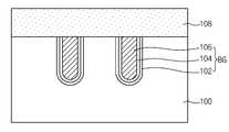
도 1은 본 발명의 실시예에 따른 반도체 소자를 도시한 단면도이다.1 is a cross-sectional view illustrating a semiconductor device in accordance with an embodiment of the present invention.
도시된 바와 같이, 게이트 형성 영역을 포함하는 활성 영역을 구비하며, 상기 게이트 형성 영역에 홈(도시안됨)이 형성된 반도체 기판(100)이 형성되어 있다. 상기 반도체 기판(100)의 활성 영역은 6F2 구조를 통해, 예를 들어, 사선 방향으로 배열되어 틸트된다.As illustrated, a
상기 홈 내에 매립 게이트(BG)가 형성되어 있다. 상기 매립 게이트(BG)는 게이트 절연막(102), 베리어막(104) 및 금속막(106)으로 이루어져 있다. 상기 게이트 절연막(102)은 산화막으로 형성하고, 상기 베리어막(104)은 TiN막으로 형성하며, 상기 금속막(106)은 W막으로 형성한다. 상기 매립 게이트(BG)는 상기 활성 영역(100a)의 표면보다 낮은 높이에 위치하는 상부면을 갖도록 형성될 수 있으며, 상기 매립 게이트(BG)는 반도체 기판(100) 내에 상기 활성 영역(100a)과 틸트된 제1방향으로 연장되게 형성한다.A buried gate BG is formed in the groove. The buried gate BG includes a
상기 반도체 기판(100) 상에 상기 매립 게이트(BG) 양측의 활성 영역 부분을 노출시키도록 절연막 패턴(108a)이 형성되어 있다. 상기 절연막 패턴(108a)은, 예를 들어, 질화막 또는 산화막일 수 있다. 상기 노출된 활성 영역 부분 상에 접합 영역(110)이 형성되어 있다.An
상기 접합 영역(110)은 단결정 실리콘층으로 이루어지며, 상기 단결정 실리콘층은 고농도로 도핑된 SEG(Selective epitaxial growth)층이다. 상기 접합 영 역(110)은 상기 절연막 패턴(108a)과 동일 두께를 가지며, 예를 들어, 400∼600Å의 두께를 갖는다. 상기 절연막 패턴(108a) 및 접합 영역(110) 상에 상기 접합 영역(110)의 드레인에 대응하는 부분을 노출시키도록 층간 절연막(112)이 형성되어 있다. 상기 층간 절연막(112)은, 예를 들어, 산화막으로 형성한다. 상기 층간 절연막(112) 상에 상기 노출된 접합 영역(110) 부분을 매립하는 도전막(114)이 형성되어 있다. 상기 도전막(114)은 붕소(B)가 이온주입된 폴리실리콘막으로 이루어진다.The
전술한 바와 같이, 본 발명은 상기 매립 게이트(BG)를 형성함으로써, 접합 영역(110)간의 거리를 증가시켜 유효 채널 길이를 증가시킬 수 있으며, 이를 통해, 단채널 효과를 감소시킬 수 있다.As described above, the present invention may increase the effective channel length by increasing the distance between the
또한, 본 발명은 상기 붕소가 이온주입된 폴리실리콘막으로 이루어진 상기 도전막(114)을 형성함으로써, 반도체 소자 동작에 중요한 역할을 하는 셀 문턱 전압을 안정적으로 확보하여 GIDL 현상을 개선할 수 있다. 따라서, 본 발명은, 누설 전류를 감소시켜 반도체 소자의 특성 및 신뢰성을 향상시킬 수 있다.In addition, according to the present invention, by forming the
도 2는 본 발명의 실시예에 따른 반도체 소자를 설명한 단면도이다. 여기서, 미설명된 도면부호 100a은 활성 영역을, 101은 소자분리막을, 그리고, BL은 비트라인을 말한다.2 is a cross-sectional view illustrating a semiconductor device in accordance with an embodiment of the present invention. Herein,
도 3a 내지 도 3f는 도 2의 A―A′선에 대응하는, 본 발명의 실시예에 따른 반도체 소자의 제조방법을 설명하기 위한 공정별 단면도로서, 이를 설명하면 다음과 같다.3A through 3F are cross-sectional views illustrating processes of manufacturing a semiconductor device in accordance with an embodiment of the present invention, corresponding to line AA ′ of FIG. 2.
도 3a를 참조하면, 게이트 형성 영역을 포함하는 활성 영역을 구비한 반도체 기판(100)의 상기 게이트 형성 영역에 홈(H)을 형성한 후, 상기 반도체 기판(100) 상에 상기 홈(H)을 매립하는 게이트 절연막(102), 베리어막(104) 및 금속막(106)을 차례로 형성한다. 상기 게이트 절연막(102)은 산화막으로 형성하고, 상기 베리어막(104)은 TiN막으로 형성하며, 상기 금속막(106)은 W막으로 형성한다.Referring to FIG. 3A, after the groove H is formed in the gate formation region of the
도 3b를 참조하면, 상기 금속막(106), 베리어막(104) 및 게이트 절연막(102)을 상기 반도체 기판(100)이 노출되도록 CMP 공정으로 제거하여 상기 홈(H) 내에 매립 게이트(BG)를 형성한다. 상기 매립 게이트(BG)는 상기 활성 영역의 표면보다 낮은 높이에 위치하는 상부면을 갖도록 형성될 수 있다. 그런 다음, 상기 매립 게이트(BG)가 형성된 반도체 기판(100) 상에 절연막(108)을 형성한다. 상기 절연막(108)은, 예를 들어, 질화막 또는 산화막으로 형성한다.Referring to FIG. 3B, the
도 3c를 참조하면, 상기 절연막(108) 상에 상기 매립 게이트(BG) 양측의 활성 영역 부분, 즉, 접합 영역이 형성될 부분을 노출시키는 감광막 패턴(도시안됨)을 형성한다. 상기 감광막 패턴을 이용해서 상기 절연막(108)을 식각하여 상기 매립 게이트(BG)를 포함한 반도체 기판(100) 상에 상기 매립 게이트(BG) 양측이 활성 영역 부분을 노출시키는 절연막 패턴(108a)을 형성한다.Referring to FIG. 3C, a photoresist pattern (not shown) is formed on the insulating
그런 다음, 상기 노출된 활성 영역 부분 상에 단결정 실리콘층으로 이루어진 SEG층을 성장시킨다. 여기서, 상기 SEG층은 상기 절연막 패턴(108a)과 동일 두께로, 예를 들어, 400∼600Å의 두께로 성장시킨다. 상기 성장된 SEG층 내에 불순물을 고농도로 이온주입하여 접합 영역(110)을 형성한다.Then, an SEG layer made of a single crystal silicon layer is grown on the exposed active region portion. Here, the SEG layer is grown to the same thickness as the insulating
전술한 바와 같이, 상기 접합 영역(110)은 상기 SEG층에 불순물을 고농도로 이온주입하여 형성하는 바, 결과적으로서, 상기 절연막 패턴(108a)과 동일, 또는, 유사 두께, 예를 들어, 400∼600Å의 두께를 갖는다.As described above, the
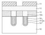
도 3d를 참조하면, 상기 절연막 패턴(108a) 및 접합 영역(110) 상에 산화막으로 이루어진 층간 절연막(112)을 형성한다. 상기 층간 절연막(112) 상에 상기 접합 영역(110)의 드레인에 대응하는 부분을 노출시키는 마스크 패턴(114)을 형성한다.Referring to FIG. 3D, an
도 3e를 참조하면, 상기 마스크 패턴을 이용해서 상기 층간 절연막(112)을 식각하여 상기 드레인 부분에 대응하는 상기 접합 영역(110)을 노출시키는 콘택홀(C)을 형성한다. 여기서, 상기 드레인 부분에 대응하는 상기 접합 영역(110)은 비트라인 콘택 형성 영역을 말한다.Referring to FIG. 3E, the
도 3f를 참조하면, 상기 식각된 층간 절연막(112) 상에 상기 콘택홀(C)을 매립하는 도전막(116)을 형성한 후, 상기 도전막(116)에 대해 할로 이온주입을 수행한다. 상기 도전막(116)은 폴리실리콘막으로 형성하며, 상기 할로 이온주입은 붕소를 이온주입한다.Referring to FIG. 3F, a
이때, 상기 할로 이온주입시, 상기 드레인 부분에 대응하는 접합 영역(110), 즉, 상기 비트라인 콘택 형성 영역을 노출시키는 상기 식각된 층간 절연막(112)으로 인하여, 소오스 부분에 대응하는 접합 영역(110), 즉, 스토리지 노드 콘택 형성 영역에 상기 붕소가 이온주입되는 것을 최소화시킬 수 있다.In this case, the junction region corresponding to the source portion may be formed due to the etched
자세하게, 상기 할로 이온주입시, 상기 드레인 부분의 접합 영역(비트라인 콘택 형성 영역; 110)에 선택적으로 이온주입을 수행할 수 있기 때문에, 반도체 소 자 동작에 중요한 역할을 하는 셀 문턱 전압을 안정적으로 확보할 수 있으므로, GIDL 현상을 개선할 수 있다. 이로 인해, 누설 전류를 감소시킬 수 있다.In detail, since ion implantation may be selectively performed on the junction region (bit line contact forming region) 110 of the drain portion during the halo ion implantation, the cell threshold voltage, which plays an important role in semiconductor element operation, is stably stabilized. As a result, the GIDL phenomenon can be improved. As a result, the leakage current can be reduced.
이후, 공지된 일련의 후속 공정들을 차례로 수행하여 본 발명의 실시예에 따른 반도체 소자의 제조를 완성한다.Thereafter, a series of well-known subsequent steps are sequentially performed to complete the manufacture of the semiconductor device according to the embodiment of the present invention.
전술한 바와 같이, 본 발명은 반도체 기판에 매립 게이트와 접합 영역을 각각 CMP 공정 및 SEG 공정을 이용하여 형성함으로써, 접합 영역간의 거리를 증가시켜 유효 채널 길이를 증가시킬 수 있으며, 이를 통해, 단채널 효과를 감소시킬 수 있다. 또한, 본 발명은 상기 매립 게이트 및 접합 영역의 형성 공정 시간을 감소시킬 수 있다.As described above, in the present invention, the buried gate and the junction region are formed in the semiconductor substrate by using the CMP process and the SEG process, respectively, thereby increasing the distance between the junction regions, thereby increasing the effective channel length. The effect can be reduced. In addition, the present invention can reduce the process time for forming the buried gate and the junction region.
게다가, 본 발명은 드레인 부분의 접합 영역(비트라인 콘택 형성 영역)에 선택적으로 이온주입을 수행하여 반도체 소자 동작에 중요한 역할을 하는 셀 문턱 전압을 안정적으로 확보할 수 있기 때문에, GIDL 현상을 개선하여 누설 전류를 감소시킬 수 있으므로, 반도체 소자의 특성 및 신뢰성을 향상시킬 수 있다.In addition, the present invention can improve the GIDL phenomenon because the cell threshold voltage, which plays an important role in semiconductor device operation, can be stably secured by selectively implanting ions into the junction region (bit line contact forming region) of the drain portion. Since the leakage current can be reduced, the characteristics and the reliability of the semiconductor element can be improved.
이상, 여기에서는 본 발명을 특정 실시예에 관련하여 도시하고 설명하였지만, 본 발명이 그에 한정되는 것은 아니며, 이하의 특허청구의 범위는 본 발명의 정신과 분야를 이탈하지 않는 한도 내에서 본 발명이 다양하게 개조 및 변형될 수 있다는 것을 당업계에서 통상의 지식을 가진 자가 용이하게 알 수 있다.As mentioned above, although the present invention has been illustrated and described with reference to specific embodiments, the present invention is not limited thereto, and the following claims are not limited to the scope of the present invention without departing from the spirit and scope of the present invention. It can be easily understood by those skilled in the art that can be modified and modified.
도 1은 본 발명의 실시예에 따른 반도체 소자를 도시한 단면도.1 is a cross-sectional view showing a semiconductor device according to an embodiment of the present invention.
도 2는 본 발명의 실시예에 따른 반도체 소자 및 그의 제조방법을 설명하기 위한 평면도.2 is a plan view illustrating a semiconductor device and a method of manufacturing the same according to an embodiment of the present invention.
도 3a 내지 도 3f는 도 2의 A―A′선에 대응하는, 본 발명의 실시예에 따른 반도체 소자의 제조방법을 설명하기 위한 공정별 단면도.3A to 3F are cross-sectional views illustrating processes for manufacturing a semiconductor device in accordance with an embodiment of the present invention, corresponding to line AA ′ of FIG. 2.
* 도면의 주요 부분에 대한 부호의 설명 *Explanation of symbols on the main parts of the drawings
100 : 반도체 기판H : 홈100: semiconductor substrate H: groove
102 : 게이트 절연막104 : 베리어막102
106 : 금속막BG : 매립 게이트106: metal film BG: buried gate
108 : 절연막108a: 절연막 패턴108: insulating
110 : SEG층112 : 층간 절연막110: SEG layer 112: interlayer insulating film
114 : 마스크 패턴C : 콘택홀114: mask pattern C: contact hole
116 : 도전막116: conductive film
Claims (15)
Translated fromKoreanPriority Applications (1)
| Application Number | Priority Date | Filing Date | Title |
|---|---|---|---|
| KR1020090023613AKR20100104900A (en) | 2009-03-19 | 2009-03-19 | Semiconductor device and method of manufacturing the same |
Applications Claiming Priority (1)
| Application Number | Priority Date | Filing Date | Title |
|---|---|---|---|
| KR1020090023613AKR20100104900A (en) | 2009-03-19 | 2009-03-19 | Semiconductor device and method of manufacturing the same |
Publications (1)
| Publication Number | Publication Date |
|---|---|
| KR20100104900Atrue KR20100104900A (en) | 2010-09-29 |
Family
ID=43009101
Family Applications (1)
| Application Number | Title | Priority Date | Filing Date |
|---|---|---|---|
| KR1020090023613AWithdrawnKR20100104900A (en) | 2009-03-19 | 2009-03-19 | Semiconductor device and method of manufacturing the same |
Country Status (1)
| Country | Link |
|---|---|
| KR (1) | KR20100104900A (en) |
Cited By (1)
| Publication number | Priority date | Publication date | Assignee | Title |
|---|---|---|---|---|
| US8785267B2 (en) | 2011-12-14 | 2014-07-22 | Samsung Electronics Co., Ltd. | Methods of manufacturing semiconductor devices including transistors |
- 2009
- 2009-03-19KRKR1020090023613Apatent/KR20100104900A/ennot_activeWithdrawn
Cited By (1)
| Publication number | Priority date | Publication date | Assignee | Title |
|---|---|---|---|---|
| US8785267B2 (en) | 2011-12-14 | 2014-07-22 | Samsung Electronics Co., Ltd. | Methods of manufacturing semiconductor devices including transistors |
Similar Documents
| Publication | Publication Date | Title |
|---|---|---|
| KR101119774B1 (en) | Semiconductor device and method of fabricating the same | |
| US8759844B2 (en) | Semiconductor device having elevated source and drain | |
| KR100855834B1 (en) | Semiconductor device and manufacturing method thereof | |
| US9608106B2 (en) | Semiconductor device and method for forming the same | |
| US8766333B2 (en) | Semiconductor device and method of manufacturing the same | |
| US8093661B2 (en) | Integrated circuit device with single crystal silicon on silicide and manufacturing method | |
| US7384842B1 (en) | Methods involving silicon-on-insulator trench memory with implanted plate | |
| KR100920045B1 (en) | Semiconductor device and manufacturing method thereof | |
| US20120007177A1 (en) | Semiconductor device and method of manufacturing the same | |
| US9269819B2 (en) | Semiconductor device having a gate and a conductive line in a pillar pattern | |
| US20080073730A1 (en) | Semiconductor device and method for formimg the same | |
| US9252216B2 (en) | Semiconductor device and method for manufacturing the same | |
| US20130059423A1 (en) | Method of manufacturing semiconductor device | |
| TWI532181B (en) | Recessed channel access transistor element and manufacturing method thereof | |
| KR20040074347A (en) | semiconductor device having a contact pad and method for a same | |
| US7368778B2 (en) | DRAM having at least three layered impurity regions between channel holes and method of fabricating same | |
| US8124479B2 (en) | Diffusing impurity ions into pillars to form vertical transistors | |
| KR20110105168A (en) | Semiconductor device and manufacturing method thereof | |
| KR20100104900A (en) | Semiconductor device and method of manufacturing the same | |
| KR100945508B1 (en) | Zero Capacitor Ram and Method of Manufacturing the Same | |
| KR100642392B1 (en) | Semiconductor device and manufacturing method thereof | |
| US20100117131A1 (en) | Transistor for Preventing or Reducing Short Channel Effect and Method for Manufacturing the Same | |
| KR20080029266A (en) | Manufacturing method of semiconductor device | |
| US7652323B2 (en) | Semiconductor device having step gates and method of manufacturing the same | |
| KR20060038744A (en) | Semiconductor element and manufacturing method thereof |
Legal Events
| Date | Code | Title | Description |
|---|---|---|---|
| PA0109 | Patent application | Patent event code:PA01091R01D Comment text:Patent Application Patent event date:20090319 | |
| PG1501 | Laying open of application | ||
| PC1203 | Withdrawal of no request for examination | ||
| WITN | Application deemed withdrawn, e.g. because no request for examination was filed or no examination fee was paid |