KR20100103154A - Thin film type solar cell, and method for manufacturing the same - Google Patents
Thin film type solar cell, and method for manufacturing the sameDownload PDFInfo
- Publication number
- KR20100103154A KR20100103154AKR1020090021625AKR20090021625AKR20100103154AKR 20100103154 AKR20100103154 AKR 20100103154AKR 1020090021625 AKR1020090021625 AKR 1020090021625AKR 20090021625 AKR20090021625 AKR 20090021625AKR 20100103154 AKR20100103154 AKR 20100103154A
- Authority
- KR
- South Korea
- Prior art keywords
- layer
- semiconductor layer
- separator
- solar cell
- forming
- Prior art date
- Legal status (The legal status is an assumption and is not a legal conclusion. Google has not performed a legal analysis and makes no representation as to the accuracy of the status listed.)
- Granted
Links
- 238000000034methodMethods0.000titleclaimsabstractdescription61
- 239000010409thin filmSubstances0.000titleclaimsabstractdescription48
- 238000004519manufacturing processMethods0.000titleclaimsabstractdescription21
- 239000004065semiconductorSubstances0.000claimsabstractdescription116
- 239000000758substrateSubstances0.000claimsabstractdescription35
- 238000000926separation methodMethods0.000claimsabstractdescription18
- 239000000463materialSubstances0.000claimsdescription15
- 239000011810insulating materialSubstances0.000claimsdescription11
- 238000007639printingMethods0.000claimsdescription10
- 230000015572biosynthetic processEffects0.000abstract1
- 239000004020conductorSubstances0.000description13
- 229910052709silverInorganic materials0.000description11
- 229910052782aluminiumInorganic materials0.000description6
- XUIMIQQOPSSXEZ-UHFFFAOYSA-NSiliconChemical compound[Si]XUIMIQQOPSSXEZ-UHFFFAOYSA-N0.000description5
- 229910052710siliconInorganic materials0.000description5
- 239000010703siliconSubstances0.000description5
- 229910006404SnO 2Inorganic materials0.000description4
- 238000005229chemical vapour depositionMethods0.000description4
- 239000011521glassSubstances0.000description4
- 229910052751metalInorganic materials0.000description4
- 239000002184metalSubstances0.000description4
- 230000005684electric fieldEffects0.000description3
- 238000004544sputter depositionMethods0.000description3
- 229910004298SiO 2Inorganic materials0.000description2
- 229910010413TiO 2Inorganic materials0.000description2
- 238000004140cleaningMethods0.000description2
- 238000005530etchingMethods0.000description2
- 238000007646gravure printingMethods0.000description2
- AMGQUBHHOARCQH-UHFFFAOYSA-Nindium;oxotinChemical compound[In].[Sn]=OAMGQUBHHOARCQH-UHFFFAOYSA-N0.000description2
- 238000007641inkjet printingMethods0.000description2
- 238000000813microcontact printingMethods0.000description2
- 229910052750molybdenumInorganic materials0.000description2
- 229910052759nickelInorganic materials0.000description2
- 239000000049pigmentSubstances0.000description2
- 229920003023plasticPolymers0.000description2
- 230000007261regionalizationEffects0.000description2
- 238000007650screen-printingMethods0.000description2
- 238000010521absorption reactionMethods0.000description1
- 238000011109contaminationMethods0.000description1
- 230000007423decreaseEffects0.000description1
- 238000010586diagramMethods0.000description1
- 230000000694effectsEffects0.000description1
- 238000000206photolithographyMethods0.000description1
- 238000005268plasma chemical vapour depositionMethods0.000description1
- 239000000126substanceSubstances0.000description1
Images


Classifications
- H—ELECTRICITY
- H10—SEMICONDUCTOR DEVICES; ELECTRIC SOLID-STATE DEVICES NOT OTHERWISE PROVIDED FOR
- H10F—INORGANIC SEMICONDUCTOR DEVICES SENSITIVE TO INFRARED RADIATION, LIGHT, ELECTROMAGNETIC RADIATION OF SHORTER WAVELENGTH OR CORPUSCULAR RADIATION
- H10F77/00—Constructional details of devices covered by this subclass
- H10F77/40—Optical elements or arrangements
- H10F77/42—Optical elements or arrangements directly associated or integrated with photovoltaic cells, e.g. light-reflecting means or light-concentrating means
- H10F77/488—Reflecting light-concentrating means, e.g. parabolic mirrors or concentrators using total internal reflection
- H—ELECTRICITY
- H10—SEMICONDUCTOR DEVICES; ELECTRIC SOLID-STATE DEVICES NOT OTHERWISE PROVIDED FOR
- H10F—INORGANIC SEMICONDUCTOR DEVICES SENSITIVE TO INFRARED RADIATION, LIGHT, ELECTROMAGNETIC RADIATION OF SHORTER WAVELENGTH OR CORPUSCULAR RADIATION
- H10F19/00—Integrated devices, or assemblies of multiple devices, comprising at least one photovoltaic cell covered by group H10F10/00, e.g. photovoltaic modules
- H10F19/30—Integrated devices, or assemblies of multiple devices, comprising at least one photovoltaic cell covered by group H10F10/00, e.g. photovoltaic modules comprising thin-film photovoltaic cells
- H10F19/31—Integrated devices, or assemblies of multiple devices, comprising at least one photovoltaic cell covered by group H10F10/00, e.g. photovoltaic modules comprising thin-film photovoltaic cells having multiple laterally adjacent thin-film photovoltaic cells deposited on the same substrate
- H10F19/33—Patterning processes to connect the photovoltaic cells, e.g. laser cutting of conductive or active layers
- H—ELECTRICITY
- H10—SEMICONDUCTOR DEVICES; ELECTRIC SOLID-STATE DEVICES NOT OTHERWISE PROVIDED FOR
- H10F—INORGANIC SEMICONDUCTOR DEVICES SENSITIVE TO INFRARED RADIATION, LIGHT, ELECTROMAGNETIC RADIATION OF SHORTER WAVELENGTH OR CORPUSCULAR RADIATION
- H10F77/00—Constructional details of devices covered by this subclass
- H10F77/20—Electrodes
- H10F77/206—Electrodes for devices having potential barriers
- H10F77/211—Electrodes for devices having potential barriers for photovoltaic cells
- Y—GENERAL TAGGING OF NEW TECHNOLOGICAL DEVELOPMENTS; GENERAL TAGGING OF CROSS-SECTIONAL TECHNOLOGIES SPANNING OVER SEVERAL SECTIONS OF THE IPC; TECHNICAL SUBJECTS COVERED BY FORMER USPC CROSS-REFERENCE ART COLLECTIONS [XRACs] AND DIGESTS
- Y02—TECHNOLOGIES OR APPLICATIONS FOR MITIGATION OR ADAPTATION AGAINST CLIMATE CHANGE
- Y02E—REDUCTION OF GREENHOUSE GAS [GHG] EMISSIONS, RELATED TO ENERGY GENERATION, TRANSMISSION OR DISTRIBUTION
- Y02E10/00—Energy generation through renewable energy sources
- Y02E10/50—Photovoltaic [PV] energy
- Y02E10/52—PV systems with concentrators
Landscapes
- Photovoltaic Devices (AREA)
Abstract
Description
Translated fromKorean본 발명은 박막형 태양전지(Solar Cell)에 관한 것으로서, 보다 구체적으로는 복수 개의 단위셀이 직렬로 연결된 구조를 갖는 박막형 태양전지에 관한 것이다.The present invention relates to a thin film solar cell, and more particularly, to a thin film solar cell having a structure in which a plurality of unit cells are connected in series.
태양전지는 반도체의 성질을 이용하여 빛 에너지를 전기 에너지로 변환시키는 장치이다.Solar cells are devices that convert light energy into electrical energy using the properties of semiconductors.
태양전지의 구조 및 원리에 대해서 간단히 설명하면, 태양전지는 P(positive)형 반도체와 N(negative)형 반도체를 접합시킨 PN접합 구조를 하고 있으며, 이러한 구조의 태양전지에 태양광이 입사되면, 입사된 태양광이 가지고 있는 에너지에 의해 상기 반도체 내에서 정공(hole) 및 전자(electron)가 발생하고, 이때, PN접합에서 발생한 전기장에 의해서 상기 정공(+)는 P형 반도체쪽으로 이동하고 상기 전자(-)는 N형 반도체쪽으로 이동하게 되어 전위가 발생하게 됨으로써 전력을 생산할 수 있게 되는 원리이다.The structure and principle of the solar cell will be briefly described. The solar cell has a PN junction structure in which a P (positive) type semiconductor and a N (negative) type semiconductor are bonded to each other. Holes and electrons are generated in the semiconductor by the energy of the incident solar light. At this time, the holes (+) are moved toward the P-type semiconductor by the electric field generated in the PN junction. Negative (-) is the principle that the electric potential is generated by moving toward the N-type semiconductor to generate power.
이와 같은 태양전지는 기판형 태양전지와 박막형 태양전지로 구분할 수 있 다.Such solar cells may be classified into a substrate type solar cell and a thin film type solar cell.
상기 기판형 태양전지는 실리콘과 같은 반도체물질 자체를 기판으로 이용하여 태양전지를 제조한 것이고, 상기 박막형 태양전지는 유리 등과 같은 기판 상에 박막의 형태로 반도체를 형성하여 태양전지를 제조한 것이다.The substrate type solar cell is a solar cell manufactured using a semiconductor material such as silicon as a substrate, and the thin film type solar cell is a solar cell manufactured by forming a semiconductor in the form of a thin film on a substrate such as glass.
상기 기판형 태양전지는 상기 박막형 태양전지에 비하여 효율이 다소 우수하기는 하지만, 공정상 두께를 최소화하는데 한계가 있고 고가의 반도체 기판을 이용하기 때문에 제조비용이 상승되는 단점이 있다.Although the substrate type solar cell is somewhat superior in efficiency to the thin film type solar cell, there is a limitation in minimizing the thickness in the process and the manufacturing cost is increased because an expensive semiconductor substrate is used.
상기 박막형 태양전지는 상기 기판형 태양전지에 비하여 효율이 다소 떨어지기는 하지만, 얇은 두께로 제조가 가능하고 저가의 재료를 이용할 수 있어 제조비용이 감소되는 장점이 있어 대량생산에 적합하다.Although the thin film type solar cell has a somewhat lower efficiency than the substrate type solar cell, the thin film solar cell is suitable for mass production because the thin film solar cell can be manufactured in a thin thickness and a low cost material can be used to reduce the manufacturing cost.
상기 박막형 태양전지는 유리 등과 같은 기판 상에 전면전극을 형성하고, 상기 전면전극 위에 반도체층을 형성하고, 상기 반도체층 위에 후면전극을 형성하여 제조된다. 여기서, 상기 전면전극은 광이 입사되는 수광면을 형성하기 때문에 상기 전면전극으로는 ZnO와 같은 투명도전물이 이용되는데, 기판이 대면적화됨에 따라 상기 투명도전물의 저항으로 인해서 전력손실이 크게 되는 문제가 발생하게 된다.The thin film solar cell is manufactured by forming a front electrode on a substrate such as glass, a semiconductor layer on the front electrode, and a back electrode on the semiconductor layer. Here, since the front electrode forms a light receiving surface on which light is incident, a transparent conductive material such as ZnO is used as the front electrode. As the substrate becomes larger, the power loss is large due to the resistance of the transparent conductive material. Will occur.
따라서, 박막형 태양전지를 복수 개의 단위셀로 나누고 복수 개의 단위셀을 직렬로 연결하는 구조로 형성함으로써 투명도전물의 저항으로 의한 전력손실을 최소화하는 방법이 고안되었다.Therefore, a method of minimizing power loss due to the resistance of the transparent conductive material has been devised by dividing the thin film solar cell into a plurality of unit cells and connecting the plurality of unit cells in series.
이하, 도면을 참조로 종래 복수 개의 단위셀이 직렬로 연결된 구조를 갖는 박막형 태양전지에 대해서 설명하기로 한다.Hereinafter, a thin film solar cell having a structure in which a plurality of unit cells are connected in series will be described with reference to the drawings.
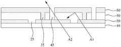
도 1은 종래 복수 개의 단위셀이 직렬로 연결된 구조를 갖는 박막형 태양전지의 개략적 단면도이다.1 is a schematic cross-sectional view of a thin film solar cell having a structure in which a plurality of unit cells are connected in series.
도 1에서 알 수 있듯이, 종래의 박막형 태양전지는, 기판(10), 전면전극(20), 반도체층(30), 및 후면전극(50)을 포함하여 이루어진다.As can be seen in FIG. 1, a conventional thin film solar cell includes a
상기 전면전극(20)은 상기 기판(10) 위에 형성되며, 제1분리부(25)를 사이에 두고 복수 개가 이격 형성된다.The
상기 반도체층(30)은 상기 전면전극(20) 위에 형성되며, 콘택부(35) 및 제2분리부(45)를 구비한다.The
상기 후면전극(50)은 상기 반도체층(30) 위에 형성되며, 상기 제2분리부(45)를 사이에 두고 복수 개가 이격 형성된다. 또한, 상기 후면전극(50)은 상기 반도체층(30)에 구비된 콘택부(35)를 통해서 상기 전면전극(20)과 연결된다.The
이와 같이, 상기 전면전극(20)은 제1분리부(25)에 의해 이격 형성되고 상기 후면전극(50)은 상기 제2분리부(45)에 의해 이격 형성됨으로써 태양전지가 복수 개의 단위셀로 구성되게 되며, 또한 상기 콘택부(35)를 통해 전면전극(20)과 후면전극(50)이 연결됨으로써 복수 개의 단위셀이 직렬로 연결되는 구조를 갖게 된다.As such, the
그러나, 종래의 박막형 태양전지는 전기에너지를 생산하는데 최대한 활용하지 못하고 손실되는 태양광이 많아서 원하는 만큼의 고효율을 달성할 수 없는 문제점이 있다.However, the conventional thin-film solar cell has a problem that can not achieve the high efficiency as desired because there is a lot of sunlight is not utilized to produce the maximum electrical energy.
즉, 고효율의 박막형 태양전지를 얻기 위해서는, 화살표(A1)와 같이 전면전극(20)을 통해 입사된 태양광이 후면전극(50)에서 반사됨으로써 반도체층(30) 내에 서의 태양광의 경로가 최대화될 필요가 있는데, 종래의 경우 화살표(A2)와 같이 제2분리부(45)를 향해 경사진 방향으로 입사되는 태양광은 반사되지 않고 그대로 외부로 방출되어 손실됨으로써 전기에너지 생산에 충분히 활용되지 못하는 문제점이 있다.That is, in order to obtain a high-efficiency thin film solar cell, as the arrow A1, sunlight incident through the
본 발명은 전술한 종래의 박막형 태양전지의 문제점을 해결하기 위해 고안된 것으로서,The present invention is designed to solve the problems of the conventional thin-film solar cell described above,
본 발명은 입사된 태양광이 그대로 외부로 방출되지 않고 다시 반도체층 내로 반사되도록 하여 반도체층 내에서의 태양광의 경로를 최대화할 수 있는 박막형 태양전지 및 그 제조방법을 제공하는 것을 목적으로 한다. 보다 구체적으로는, 본 발명은 제2분리부를 향해 경사진 방향으로 입사되는 태양광이 반도체층 내로 반사되도록 함으로써, 손실되는 태양광을 최소화하여 전지효율을 증진시킬 수 있는 박막형 태양전지 및 그 제조방법을 제공하는 것을 목적으로 한다.It is an object of the present invention to provide a thin film solar cell and a method of manufacturing the same, which can maximize the path of sunlight in the semiconductor layer by allowing the incident sunlight to be reflected back into the semiconductor layer without being emitted to the outside. More specifically, the present invention is a thin-film solar cell and a method for manufacturing the thin film solar cell that can improve the battery efficiency by minimizing the lost solar light by allowing the incident light in the direction inclined toward the second separation portion reflected into the semiconductor layer The purpose is to provide.
본 발명은 상기 목적을 달성하기 위해서, 기판 위에 제1분리부에 의해 이격 형성되는 전면전극; 상기 전면전극 위에서, 콘택부 및 제2분리부를 구비하면서 형성되는 반도체층; 상기 콘택부를 통해 상기 전면전극과 전기적으로 연결되며, 상기 제2분리부에 의해 이격 형성되는 후면전극; 및 상기 제2분리부 내에 형성되어 상기 제2분리부로 입사되는 태양광을 상기 반도체층으로 반사시키기 위한 반사층을 포함하여 이루어진 박막형 태양전지를 제공한다.The present invention, in order to achieve the above object, the front electrode formed spaced apart by the first separator on the substrate; A semiconductor layer formed on the front electrode with a contact portion and a second separator; A rear electrode electrically connected to the front electrode through the contact part and spaced apart by the second separator; And a reflective layer formed in the second separator and reflecting sunlight incident on the second separator to the semiconductor layer.
여기서, 상기 반사층은 단위셀 간의 쇼트를 방지하기 위해서 절연물질로 이루어질 수 있다.Here, the reflective layer may be made of an insulating material to prevent short between unit cells.
상기 반도체층과 상기 후면전극 사이에 투명도전층이 추가로 형성될 수 있 다. 이때, 상기 투명도전층은 상기 콘택부 내에 형성되고 상기 후면전극은 상기 투명도전층을 통해 상기 전면전극과 전기적으로 연결될 수도 있고, 또는 상기 투명도전층은 상기 반도체층과 동일한 패턴으로 형성되고 상기 후면전극은 상기 전면전극과 직접 연결될 수도 있다.A transparent conductive layer may be further formed between the semiconductor layer and the back electrode. In this case, the transparent conductive layer is formed in the contact portion and the back electrode may be electrically connected to the front electrode through the transparent conductive layer, or the transparent conductive layer is formed in the same pattern as the semiconductor layer and the back electrode is the It may also be directly connected to the front electrode.
본 발명은 또한 기판 위에 제1분리부에 의해 이격되는 전면전극을 형성하는 공정; 상기 전면전극 위에 콘택부를 구비한 반도체층을 형성하는 공정; 상기 반도체층 위에서 상기 콘택부를 통해 상기 전면전극과 전기적으로 연결되는 후면전극층을 형성하는 공정; 상기 후면전극층의 소정 영역을 제거하여 제2분리부를 형성하는 공정; 및 상기 제2분리부로 입사되는 태양광을 상기 반도체층으로 반사시키기 위해서, 상기 제2분리부 내에 반사층을 형성하는 공정을 포함하여 이루어진 박막형 태양전지의 제조방법을 제공한다.The present invention also provides a process for forming a front electrode spaced apart by a first separator on a substrate; Forming a semiconductor layer having a contact portion on the front electrode; Forming a back electrode layer electrically connected to the front electrode through the contact portion on the semiconductor layer; Removing a predetermined region of the back electrode layer to form a second separator; And forming a reflective layer in the second separator in order to reflect the sunlight incident on the second separator into the semiconductor layer.
여기서, 상기 반도체층과 후면전극층 사이에 투명도전층을 형성하는 공정을 추가로 포함할 수 있다. 이때, 상기 콘택부를 구비한 반도체층을 형성하는 공정 이후에 상기 기판 전면에 투명도전층 및 후면전극층을 차례로 형성하고 그 후에 상기 투명도전층 및 후면전극층의 소정 영역을 제거하여 상기 제2분리부를 형성할 수 있다. 또는, 상기 반도체층 위에 상기 반도체층과 동일한 패턴으로 투명도전층을 형성하고 그 후에 상기 투명도전층 위에 상기 후면전극층을 형성할 수도 있다.The method may further include forming a transparent conductive layer between the semiconductor layer and the back electrode layer. In this case, after the process of forming the semiconductor layer having the contact portion, the transparent conductive layer and the rear electrode layer may be sequentially formed on the front surface of the substrate, and then, the predetermined region of the transparent conductive layer and the rear electrode layer may be removed to form the second separator. have. Alternatively, the transparent conductive layer may be formed on the semiconductor layer in the same pattern as the semiconductor layer, and then the back electrode layer may be formed on the transparent conductive layer.
본 발명은 또한 기판 위에 제1분리부에 의해 이격되는 전면전극을 형성하는 공정; 상기 전면전극 위에 콘택부 및 제2분리부를 구비한 반도체층을 형성하는 공정; 상기 콘택부를 통해 상기 전면전극과 전기적으로 연결되며, 상기 제2분리부에 의해 이격되는 후면전극을 형성하는 공정; 및 상기 제2분리부로 입사되는 태양광을 상기 반도체층으로 반사시키기 위해서, 상기 제2분리부 내에 반사층을 형성하는 공정을 포함하여 이루어진 박막형 태양전지의 제조방법을 제공한다.The present invention also provides a process for forming a front electrode spaced apart by a first separator on a substrate; Forming a semiconductor layer having a contact portion and a second separator on the front electrode; Forming a rear electrode electrically connected to the front electrode through the contact part and spaced apart from the second separator; And forming a reflective layer in the second separator in order to reflect the sunlight incident on the second separator into the semiconductor layer.
여기서, 상기 반도체층과 상기 후면전극 사이에 상기 반도체층과 동일한 패턴으로 투명도전층을 형성하는 공정을 추가로 포함할 수 있다.The method may further include forming a transparent conductive layer between the semiconductor layer and the back electrode in the same pattern as the semiconductor layer.
상기 반도체층을 형성하는 공정은 상기 전면전극을 포함한 기판 전면에 반도체물질층을 도포한 후 1회의 레이저조사에 의해 상기 콘택부 및 제2분리부를 동시에 형성하는 공정으로 이루어질 수 있다.The process of forming the semiconductor layer may be performed by applying a semiconductor material layer on the entire surface of the substrate including the front electrode and simultaneously forming the contact portion and the second separation portion by one laser irradiation.
상기 후면전극을 형성하는 공정은 인쇄법을 이용하여 수행할 수 있다.The process of forming the back electrode may be performed using a printing method.
상기 반사층을 형성하는 공정은 단위셀 간의 쇼트를 방지하기 위해서 절연물질을 이용하여 형성할 수 있다.The process of forming the reflective layer may be formed using an insulating material to prevent short between unit cells.
상기 반사층을 형성하는 공정은 인쇄법을 이용하여 수행할 수 있다.The process of forming the reflective layer may be performed using a printing method.
상기와 같은 본 발명에 따르면 다음과 같은 효과가 있다.According to the present invention as described above has the following effects.
첫째, 본 발명은 제2분리부 내에 반사층을 형성함으로써, 제2분리부로 입사되는 태양광을 반도체층으로 반사시켜 반도체층 내에서의 태양광의 경로가 증가되어 전지효율이 증진되는 효과가 있다.First, the present invention forms a reflective layer in the second separator, thereby reflecting sunlight incident on the second separator into the semiconductor layer, thereby increasing the path of sunlight in the semiconductor layer, thereby improving battery efficiency.
둘째, 본 발명의 일 실시예에 따르면, 인쇄법을 이용하여 소정 패턴의 후면전극을 형성하기 때문에 패턴 형성을 위한 레이저스크라이빙 공정 회수를 줄일 수 있어 공정이 간단해지고 생산성이 향상되는 효과가 있다.Second, according to an embodiment of the present invention, since the back electrode of a predetermined pattern is formed using a printing method, the number of laser scribing processes for pattern formation can be reduced, thereby simplifying the process and improving productivity. .
이하, 도면을 참조로 본 발명의 바람직한 실시예에 대해서 상세히 설명하기로 한다.Hereinafter, preferred embodiments of the present invention will be described in detail with reference to the drawings.
<박막형 태양전지><Thin Film Solar Cell>
도 2는 본 발명의 일 실시예에 따른 박막형 태양전지의 개략적인 단면도이다.2 is a schematic cross-sectional view of a thin film solar cell according to an embodiment of the present invention.
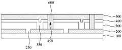
도 2에서 알 수 있듯이, 본 발명의 일 실시예에 따른 박막형 태양전지는 기판(100), 전면전극(200), 반도체층(300), 후면전극(500), 및 반사층(600)을 포함하여 이루어진다.As can be seen in Figure 2, the thin-film solar cell according to an embodiment of the present invention includes a
상기 기판(100)으로는 유리 또는 투명한 플라스틱을 이용할 수 있다.Glass or transparent plastic may be used as the
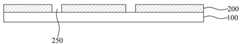
상기 전면전극(200)은 상기 기판(100) 위에 형성되며, 제1분리부(250)에 의해 이격 형성된다. 상기 제1분리부(250)는 상기 전면전극(200)을 단위셀 별로 분리하는 역할을 하는 것이다.The
상기 전면전극(200)은 ZnO, ZnO:B, ZnO:Al, SnO2, SnO2:F, ITO(Indium Tin Oxide) 등과 같은 투명한 도전물질로 이루어질 수 있다.The
상기 전면전극(200)은 태양광이 입사되는 면에 형성되기 때문에 입사되는 태양광이 태양전지 내부로 최대한 흡수될 수 있도록 하는 것이 중요하며, 이를 위해서 상기 전면전극(200)의 표면을 요철구조로 형성할 수 있다. 이와 같은 전면전극(200)의 표면을 요철구조로 형성할 경우 입사되는 태양광이 태양전지 외부로 반 사되는 비율은 감소하게 되며, 그와 더불어 입사되는 태양광의 산란에 의해 태양전지 내부로 태양광이 흡수되는 비율은 증가하게 되어, 태양전지의 효율이 증진되는 효과가 있다.Since the
상기 반도체층(300)은 상기 전면전극(200) 위에 형성되며, 콘택부(350) 및 제2분리부(450)를 구비하여 형성된다. 상기 콘택부(350) 및 제2분리부(450)는 서로 이격되도록 형성된다. 상기 콘택부(350)는 복수 개의 단위셀을 직렬로 연결하기 위한 통로로서, 구체적으로는 서로 이웃하는 전면전극(200)과 후면전극(500)을 전기적으로 연결하는 통로이다. 상기 제2분리부(450)는 상기 후면전극(500)을 단위셀 별로 분리하는 역할을 하는 것이다.The
상기 반도체층(300)은 P형 반도체층, I형 반도체층 및 N형 반도체층이 순서대로 적층된 PIN구조의 실리콘계 반도체물질로 이루어질 수 있다. 이와 같이 상기 반도체층(300)을 PIN구조로 형성하게 되면, I형 반도체층이 P형 반도체층과 N형 반도체층에 의해 공핍(depletion)이 되어 내부에 전기장이 발생하게 되고, 태양광에 의해 생성되는 정공 및 전자가 상기 전기장에 의해 드리프트(drift)되어 각각 P형 반도체층 및 N형 반도체층에서 수집되게 된다. 한편, 상기 반도체층(300)을 PIN구조로 형성할 경우에는 P형 반도체층을 먼저 형성하고, 그 후에 I형 반도체층 및 N형 반도체층을 순서대로 형성하는 것이 바람직한데, 그 이유는 일반적으로 정공의 드리프트 이동도(drift mobility)가 전자의 드리프트 이동도에 의해 낮기 때문에 입사광에 의한 수집효율을 극대화하기 위해서 P형 반도체층을 수광면에 가깝게 형성하기 위함이다.The
상기 후면전극(500)은 상기 반도체층(300) 위에 형성되며, 상기 콘택부(350)를 통해 상기 전면전극(200)과 전기적으로 연결되어 복수 개의 단위셀이 직렬로 연결되게 된다. 또한, 상기 후면전극(500)은 상기 제2분리부(450)에 의해 이격 형성된다. 상기 후면전극(500)은 Ag, Al, Ag+Mo, Ag+Ni, Ag+Cu 등과 같은 금속으로 이루어질 수 있다.The
상기 반사층(600)은 상기 제2분리부(450) 내에 형성되어, 화살표(B)와 같이 상기 제2분리부(450)로 입사되는 태양광을 상기 반도체층(300)으로 반사시키는 역할을 한다. 이와 같이 반사층(600)에 의해 태양광이 반사됨으로써 상기 반도체층(300) 내에서의 태양광의 경로가 증가되게 되고, 그로 인해서 손실되는 태양광이 최소화되어 전지효율이 증진되게 된다.The
상기 반사층(600)은 태양광을 상기 반도체층(300)으로 반사시키는 역할을 하기 때문에, 상기 제2분리부(450) 내에서 소정 높이로 형성되면 충분하고 반드시 후면전극(500)의 상단과 동일한 높이로 형성될 필요는 없다. 즉, 상기 반사층(600)은 상기 제2분리부(450) 내에서 상기 반도체층(300)의 상단과 동일한 높이로 형성될 수도 있고, 경우에 따라서는 상기 반도체층(300)의 상단보다 높은 높이 또는 낮은 높이로 형성될 수 있다.Since the
상기 반사층(600)으로 도전물질을 이용하게 되면 제2분리부(450)에 의해 단위셀 별로 분리되어야 하는 후면전극(500)들이 전기적으로 연결되어 쇼트가 발생하게 된다. 따라서, 상기 반사층(600)은 단위셀 간의 쇼트를 방지하기 위해서 절연물 질을 이용하여 형성된다. 상기 반사층(600)으로 이용되는 절연물질의 예로는 SiO2계 물질 또는 안료용 TiO2계 물질 등의 백색 반사 절연물질을 들 수 있다.When the conductive material is used as the
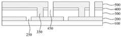
도 3a 및 도 3b는 본 발명의 다른 실시예에 따른 박막형 태양전지의 개략적인 단면도로서, 이는 상기 반도체층(300)과 상기 후면전극(500) 사이에 투명도전층(400)이 추가로 형성된 것을 제외하고, 전술한 도 2에 따른 박막형 태양전지와 동일하다. 따라서, 동일한 구성에 대해서는 동일한 도면부호를 부여하였고, 동일한 구성에 대한 구체적인 설명은 생략하기로 한다.3A and 3B are schematic cross-sectional views of a thin film solar cell according to another exemplary embodiment of the present invention, except that a transparent
도 3a 및 도 3b에서와 같이, 상기 반도체층(300)과 상기 후면전극(500) 사이에 투명도전층(400)이 추가로 형성되면, 상기 반도체층(300)을 투과한 태양광이 투명도전층(400)을 통과하면서 산란을 통해 다양한 각으로 진행하게 되어 상기 후면전극(500)에서 반사되어 반도체층(300)으로 재입사되는 광의 비율이 증가될 수 있고, 그에 따라 전지효율이 증가된다. 상기 투명도전층(400a)은 ZnO, ZnO:B, ZnO:Al, Ag와 같은 투명한 도전물질로 이루어질 수 있다.3A and 3B, when the transparent
도 3a에서 알 수 있듯이, 상기 투명도전층(400)은 상기 반도체층(300)과 상기 후면전극(500) 사이에 형성되면서, 특히 상기 콘택부(350) 내에 형성될 수 있다. 이 경우, 상기 후면전극(500)은 상기 콘택부(350) 내에 형성된 투명도전층(400)을 통해 상기 전면전극(200)과 전기적으로 연결된다.As can be seen in FIG. 3A, the transparent
도 3b에서 알 수 있듯이, 상기 투명도전층(400)은 상기 반도체층(300)과 상기 후면전극(500) 사이에 형성되면서, 특히 상기 반도체층(300)과 동일한 패턴으로 형성될 수 있다. 이 경우, 상기 후면전극(500)은 상기 콘택부(350) 내에 형성되어 상기 전면전극(200)과 직접 연결된다.As shown in FIG. 3B, the transparent
<박막형 태양전지 제조방법><Thin Film Solar Cell Manufacturing Method>
도 4a 내지 도 4e는 본 발명의 일 실시예에 따른 박막형 태양전지의 제조공정을 도시한 단면도이다.4A to 4E are cross-sectional views illustrating a manufacturing process of a thin film solar cell according to an embodiment of the present invention.
우선, 도 4a에서 알 수 있듯이, 기판(100) 위에 제1분리부(250)에 의해 이격되는 전면전극(200)을 형성한다.First, as shown in FIG. 4A, the
상기 전면전극(200)은 유리 또는 투명한 플라스틱과 같은 기판(100) 전면에 스퍼터링(Sputtering)법 또는 MOCVD(Metal Organic Chemical Vapor Deposition)법 등을 이용하여 ZnO, ZnO:B, ZnO:Al, SnO2, SnO2:F, ITO(Indium Tin Oxide) 등과 같은 투명한 도전물질층을 적층한 후, 레이저 스크라이빙법(Laser Scribing)을 이용하여 상기 적층된 투명한 도전물질층의 소정영역을 제거하여 제1분리부(250)를 형성하는 공정을 통해 형성할 수 있다.The
상기 전면전극(200)의 표면을 요철구조로 형성하기 위해서 상기 전면전극(200)에 텍스처(texturing) 가공공정을 추가로 수행할 수 있다. 상기 텍스처 가공공정은 포토리소그라피법(photolithography)을 이용한 식각공정, 화학용액을 이용한 이방성 식각공정(anisotropic etching), 또는 기계적 스크라이빙(mechanical scribing)을 이용한 홈 형성 공정 등을 통해 수행할 수 있다.A texturing process may be additionally performed on the
다음, 도 4b에서 알 수 있듯이, 상기 전면전극(200) 위에 콘택부(350)를 구 비한 반도체층(300)을 형성한다.Next, as shown in FIG. 4B, the
상기 반도체층(300)은 실리콘계 반도체물질을 플라즈마 CVD법 등을 이용하여 P형 반도체층, I형 반도체층 및 N형 반도체층이 순서대로 적층된 PIN구조를 형성한 후, 레이저 스크라이빙법(Laser Scribing)을 이용하여 상기 반도체물질의 소정영역을 제거하여 콘택부(350)를 형성하는 공정을 통해 형성할 수 있다. 한편, 상기 반도체층(300)을 PIN구조로 형성할 경우에는 P형 반도체층을 먼저 적층하고, 그 후에 I형 반도체층 및 N형 반도체층을 순서대로 적층하는 것이 바람직함은 전술한 바와 동일하다.The
다음, 도 4c에서 알 수 있듯이, 상기 반도체층(300) 위에 투명도전층(400a) 및 후면전극층(500a)을 순서대로 적층한다. 그리하면, 상기 후면전극층(500a)이 상기 콘택부(350) 내에 형성된 투명도전층(400a)을 통해 상기 전면전극(200)과 전기적으로 연결된다.Next, as can be seen in FIG. 4C, the transparent
상기 투명도전층(400a)은 ZnO, ZnO:B, ZnO:Al, Ag와 같은 투명한 도전물질을 스퍼터링(Sputtering)법 또는 MOCVD(Metal Organic Chemical Vapor Deposition)법 등을 이용하여 적층할 수 있다. 다만, 상기 투명도전층(400a)은 생략하는 것도 가능하며, 이 경우, 상기 후면전극층(500a) 만이 적층되고 그에 따라 상기 후면전극층(500a)이 상기 콘택부(350)를 통해 상기 전면전극(200)과 직접 연결된다.The transparent
상기 후면전극층(500a)은 Ag, Al, Ag+Mo, Ag+Ni, Ag+Cu 등과 같은 금속을 스퍼터링(Sputtering)법 또는 MOCVD(Metal Organic Chemical Vapor Deposition)법 등을 이용하여 적층할 수 있다.The
다음, 도 4d에서 알 수 있듯이, 상기 반도체층(300), 투명도전층(400a) 및 후면전극층(500a)의 소정 영역을 제거하여 제2분리부(450)를 형성한다. 그리하면, 상기 제2분리부(450)에 의해 이격되는 투명도전층(400) 및 후면전극(500) 패턴이 완성된다. 상기 제2분리부(450)는 레이저 스크라이빙법(Laser Scribing)을 이용하여 형성할 수 있다Next, as shown in FIG. 4D, predetermined regions of the
다음, 도 4e에서 알 수 있듯이, 상기 제2분리부(450)로 입사되는 태양광을 상기 반도체층(300)으로 반사시키기 위해서, 상기 제2분리부(450) 내에 반사층(600)을 형성한다.Next, as shown in FIG. 4E, in order to reflect the sunlight incident to the
상기 반사층(600)은 단위셀 별로 분리되어야 하는 후면전극(500)들이 전기적으로 연결되어 쇼트가 발생하는 것을 방지하기 위해서 SiO2계 물질 또는 안료용 TiO2계 물질 등의 백색 반사 절연물질을 이용하여 형성하며, 이와 같은 절연물질을 스크린 인쇄법(screen printing), 잉크젯 인쇄법(inkjet printing), 그라비아 인쇄법(gravure printing) 또는 미세접촉 인쇄법(microcontact printing) 등과 같은 인쇄법을 이용하여 형성할 수 있다. 다만, 상기 반사층(600)은 인쇄법 이외에 화학기상증착법 등을 이용하여 기판 전면에 절연물질을 도포한 후 상기 제2분리부(450) 이외의 영역에 도포된 절연물질을 제거하는 방법으로 형성할 수도 있다.The
상기 반사층(600)은 상기 후면전극(500)의 상단과 동일한 높이로 형성할 수도 있고, 상기 반도체층(300)의 상단과 동일한 높이로 형성할 수도 있고, 경우에 따라서는 상기 반도체층(300)의 상단보다 높은 높이 또는 낮은 높이로 형성할 수도 있다.The
도 5a 내지 도 5e는 본 발명의 다른 실시예에 따른 박막형 태양전지의 제조공정을 도시한 단면도로서, 이하, 전술한 실시예와 동일한 구성에 대한 구체적인 설명은 생략하기로 한다.5A to 5E are cross-sectional views illustrating a manufacturing process of a thin film solar cell according to another exemplary embodiment of the present invention. Hereinafter, a detailed description of the same configuration as the aforementioned exemplary embodiment will be omitted.
우선, 도 5a에서 알 수 있듯이, 기판(100) 위에 제1분리부(250)에 의해 이격되는 전면전극(200)을 형성한다.First, as shown in FIG. 5A, the
다음, 도 5b에서 알 수 있듯이, 상기 전면전극(200) 위에 콘택부(350)를 구비하면서 순서대로 적층된 반도체층(300) 및 투명도전층(400)을 형성한다.Next, as shown in FIG. 5B, the
상기 반도체층(300) 및 투명도전층(400)은 상기 전면전극(200) 위에 PIN구조의 실리콘계 반도체물질을 적층하고, 그 후에 ZnO, ZnO:B, ZnO:Al, Ag와 같은 투명한 도전물질을 적층한 후, 상기 반도체물질 및 투명한 도전물질의 소정영역을 레이저 스크라이빙법(Laser Scribing)을 이용하여 제거하여 콘택부(350)를 형성하는 공정을 통해 형성할 수 있다. 이와 같은 공정에 의할 때, 상기 반도체층(300) 및 투명도전층(400)은 동일한 패턴으로 형성된다.The
다음, 도 5c에서 알 수 있듯이, 상기 투명도전층(400) 위에 후면전극층(500a)을 형성한다. 그리하면, 상기 후면전극층(500a)이 상기 콘택부(350) 내에 적층되어 상기 전면전극(200)과 직접 연결된다.Next, as can be seen in Figure 5c, to form a back electrode layer (500a) on the transparent conductive layer (400). Then, the
다음, 도 5d에서 알 수 있듯이, 상기 반도체층(300), 투명도전층(400) 및 후면전극층(500a)의 소정 영역을 제거하여 제2분리부(450)를 형성한다. 그리하면, 상기 제2분리부(450)에 의해 이격되는 후면전극(500) 패턴이 완성된다.Next, as shown in FIG. 5D, predetermined regions of the
다음, 도 5e에서 알 수 있듯이, 상기 제2분리부(450) 내에 반사층(600)을 형성한다.Next, as shown in FIG. 5E, the
도 6a 내지 도 6d는 본 발명의 또 다른 실시예에 따른 박막형 태양전지의 제조공정을 도시한 단면도로서, 이하, 전술한 실시예와 동일한 구성에 대한 구체적인 설명은 생략하기로 한다.6A to 6D are cross-sectional views illustrating a manufacturing process of a thin film solar cell according to still another embodiment of the present invention. Hereinafter, a detailed description of the same configuration as the above-described embodiment will be omitted.
우선, 도 6a에서 알 수 있듯이, 기판(100) 위에 제1분리부(250)에 의해 이격되는 전면전극(200)을 형성한다.First, as shown in FIG. 6A, the
다음, 도 6b에서 알 수 있듯이, 상기 전면전극(200) 위에 콘택부(350) 및 제2분리부(450)를 구비하면서 순서대로 적층된 반도체층(300) 및 투명도전층(400)을 형성한다.Next, as shown in FIG. 6B, the
상기 반도체층(300) 및 투명도전층(400)은 상기 전면전극(200) 위에 PIN구조의 실리콘계 반도체물질을 적층하고, 그 후에 ZnO, ZnO:B, ZnO:Al, Ag와 같은 투명한 도전물질을 적층한 후, 상기 반도체물질 및 투명한 도전물질의 소정영역을 레이저 스크라이빙법(Laser Scribing)을 이용하여 제거하여 콘택부(350) 및 제2분리부(450)를 형성하는 공정을 통해 형성할 수 있다. 이와 같은 공정에 의할 때, 상기 반도체층(300) 및 투명도전층(400)은 동일한 패턴으로 형성된다. 다만, 상기 투명도전층(400)은 생략하는 것도 가능하다.The
상기 콘택부(350) 및 제2분리부(450)는 1회의 레이저 빔 조사를 통해 동시에 형성할 수 있다.The
도 7은 본 발명의 일 실시예에 따른 레이저 스크라이빙 장비의 개략적인 모 식도로서, 도 7에서 알 수 있듯이, 본 발명에 따른 레이저 스크라이빙 장비는 레이저 발진기(700), 제1미러(710), 제2미러(720), 제1렌즈(730), 및 제2렌즈(740)로 이루어진다. 상기 레이저 발진기(700)에서 레이저 빔이 방출되면, 방출된 레이저 빔이 상기 제1미러(710)로 입사된다. 이때, 상기 제1미러(710)는 입사되는 레이저 빔의 일부, 바람직하게는 절반은 통과시키고 입사되는 레이저 빔의 나머지는 반사시킨다. 따라서, 상기 제1미러(710)에서 통과된 레이저 빔은 상기 제1렌즈(730)를 통해 대상물에 조사되고, 상기 제1미러(710)에서 반사된 레이저 빔은 상기 제2미러(720)를 거쳐 상기 제2렌즈(740)를 통해 대상물에 조사된다. 이때, 상기 제2미러(720)는 입사되는 레이저 빔의 전부를 반사시킨다.7 is a schematic diagram of a laser scribing equipment according to an embodiment of the present invention, as can be seen in Figure 7, the laser scribing equipment according to the present invention is a
결국, 상기 1개의 레이저 발진기(700)에서 방출된 레이저 빔은 2개로 분할되어 조사되기 때문에, 이와 같이 2개로 분할된 레이저 빔에 의해 상기 콘택부(350) 및 제2분리부(450)를 동시에 형성할 수 있게 된다.As a result, since the laser beam emitted from the one
다음, 도 6c에서 알 수 있듯이, 상기 콘택부(350)를 통해 상기 전면전극(200)과 전기적으로 연결되며 상기 제2분리부(450)에 의해 이격되는 후면전극(500)을 형성한다.Next, as can be seen in FIG. 6C, the
이와 같은 후면전극(500)은 스크린 인쇄법(screen printing), 잉크젯 인쇄법(inkjet printing), 그라비아 인쇄법(gravure printing) 또는 미세접촉 인쇄법(microcontact printing) 등과 같은 인쇄법을 이용하여 한번의 공정으로 형성할 수 있다.The
이와 같이 인쇄법을 이용하여 후면전극(500)을 형성하게 되면, 패턴 형성을 위한 레이저스크라이빙 공정 회수를 줄일 수 있어 공정이 간단해지고 생산성이 향상되는 효과가 있다. 즉, 레이저 스크라이빙 공정을 수행하게 되면 공정 중에 발생하는 잔유물이 기판에 잔존하여 기판이 오염될 우려가 커지고, 기판의 오염을 방지하기 위해 세정공정을 추가할 경우 그만큼 공정이 복잡해지고 생산성이 떨어지게 되는 문제점이 있는데, 상기와 같이 인쇄법을 이용하여 후면전극(500)을 형성하게 되면 레이저 스크라이빙 공정이 필요하지 않게 되어 기판이 오염될 우려가 작아지고 추가 세정공정이 요하지 않아 공정이 간단해지는 장점이 있다.When the
다음, 도 6d에서 알 수 있듯이, 상기 제2분리부(450) 내에 반사층(600)을 형성한다.Next, as shown in FIG. 6D, the
도 1은 종래 복수 개의 단위셀이 직렬로 연결된 구조를 갖는 박막형 태양전지의 개략적 단면도.1 is a schematic cross-sectional view of a thin-film solar cell having a structure in which a plurality of conventional unit cells are connected in series.
도 2는 본 발명의 일 실시예에 따른 박막형 태양전지의 개략적인 단면도.2 is a schematic cross-sectional view of a thin film solar cell according to an embodiment of the present invention.
도 3a 및 도 3b는 본 발명의 다른 실시예에 따른 박막형 태양전지의 개략적인 단면도.3A and 3B are schematic cross-sectional views of a thin film solar cell according to another embodiment of the present invention.
도 4a 내지 도 4e는 본 발명의 일 실시예에 따른 박막형 태양전지의 제조공정을 도시한 단면도.4A to 4E are cross-sectional views illustrating a manufacturing process of a thin film solar cell according to an embodiment of the present invention.
도 5a 내지 도 5e는 본 발명의 다른 실시예에 따른 박막형 태양전지의 제조공정을 도시한 단면도.5A to 5E are cross-sectional views illustrating a manufacturing process of a thin film solar cell according to another embodiment of the present invention.
도 6a 내지 도 6d는 본 발명의 또 다른 실시예에 따른 박막형 태양전지의 제조공정을 도시한 단면도.6A to 6D are cross-sectional views illustrating a manufacturing process of a thin film solar cell according to still another embodiment of the present invention.
<도면의 주요부의 부호에 대한 설명>DESCRIPTION OF THE REFERENCE NUMERALS OF THE DRAWINGS FIG.
100: 기판 200: 전면전극100: substrate 200: front electrode
250: 제1분리부 300: 반도체층250: first separator 300: semiconductor layer
350: 콘택부 400: 투명도전층350: contact portion 400: transparent conductive layer
450: 제2분리부 500: 후면전극450: second separator 500: rear electrode
600: 반사층600: reflective layer
Claims (15)
Translated fromKoreanPriority Applications (1)
| Application Number | Priority Date | Filing Date | Title |
|---|---|---|---|
| KR1020090021625AKR101512114B1 (en) | 2009-03-13 | 2009-03-13 | Thin film solar cell and its manufacturing method |
Applications Claiming Priority (1)
| Application Number | Priority Date | Filing Date | Title |
|---|---|---|---|
| KR1020090021625AKR101512114B1 (en) | 2009-03-13 | 2009-03-13 | Thin film solar cell and its manufacturing method |
Publications (2)
| Publication Number | Publication Date |
|---|---|
| KR20100103154Atrue KR20100103154A (en) | 2010-09-27 |
| KR101512114B1 KR101512114B1 (en) | 2015-04-16 |
Family
ID=43007978
Family Applications (1)
| Application Number | Title | Priority Date | Filing Date |
|---|---|---|---|
| KR1020090021625AActiveKR101512114B1 (en) | 2009-03-13 | 2009-03-13 | Thin film solar cell and its manufacturing method |
Country Status (1)
| Country | Link |
|---|---|
| KR (1) | KR101512114B1 (en) |
Family Cites Families (1)
| Publication number | Priority date | Publication date | Assignee | Title |
|---|---|---|---|---|
| JP4929660B2 (en) | 2005-09-27 | 2012-05-09 | ソニー株式会社 | Dye-sensitized photoelectric conversion element, photoelectric conversion element module, electronic device, moving object, and power generation system |
- 2009
- 2009-03-13KRKR1020090021625Apatent/KR101512114B1/enactiveActive
Also Published As
| Publication number | Publication date |
|---|---|
| KR101512114B1 (en) | 2015-04-16 |
Similar Documents
| Publication | Publication Date | Title |
|---|---|---|
| TWI387115B (en) | Thin film type solar cell and manufacturing method thereof | |
| KR101301664B1 (en) | The method for manufacturing Thin film type Solar Cell, and Thin film type Solar Cell made by the method | |
| KR101031246B1 (en) | Thin film type solar cell, manufacturing method thereof, and thin film type solar cell module and solar power generation system using same | |
| CN101604713B (en) | Thin film type solar cell and method for manufacturing the same | |
| CN101651163B (en) | Thin film type solar cell and method for manufacturing the same | |
| US20100252109A1 (en) | Thin film type solar cell and method for manufacturing the same | |
| CN101919067B (en) | Thin film type solar cell and method for manufacturing the same | |
| CN108235789A (en) | Thin film solar cell and its manufacturing method | |
| KR101368902B1 (en) | Thin film type Solar Cell and Method for manufacturing the same | |
| CN103081123A (en) | Device for generating solar power and method for manufacturing same | |
| CN101546786A (en) | Thin film type solar cell, and method for manufacturing the same | |
| KR101368903B1 (en) | Thin film type Solar Cell, and Method for manufacturing the same | |
| KR20100004540A (en) | Thin film type solar cell, and method for manufacturing the same | |
| KR20090125675A (en) | Thin film type solar cell and manufacturing method thereof | |
| KR20090029883A (en) | Thin film type solar cell and manufacturing method thereof | |
| KR101476125B1 (en) | Thin film solar cell and its manufacturing method | |
| KR101033286B1 (en) | Thin film type solar cell and manufacturing method thereof | |
| KR101512114B1 (en) | Thin film solar cell and its manufacturing method | |
| KR101425890B1 (en) | Thin film type Solar Cell and Method for manufacturing the same | |
| KR101032433B1 (en) | Thin film type Solar Cell and Method for manufacturing the same | |
| KR100973676B1 (en) | Thin film type solar cell and manufacturing method thereof | |
| WO2009082141A2 (en) | Thin film type solar cell and method for manufacturing the same | |
| KR20100006246A (en) | Thin film type solar cell, and method for manufacturing the same | |
| KR100977726B1 (en) | Thin film type solar cell and manufacturing method thereof | |
| KR20100037861A (en) | Thin film type solar cell and method for manufacturing the same |
Legal Events
| Date | Code | Title | Description |
|---|---|---|---|
| PA0109 | Patent application | Patent event code:PA01091R01D Comment text:Patent Application Patent event date:20090313 | |
| PG1501 | Laying open of application | ||
| A201 | Request for examination | ||
| PA0201 | Request for examination | Patent event code:PA02012R01D Patent event date:20140219 Comment text:Request for Examination of Application Patent event code:PA02011R01I Patent event date:20090313 Comment text:Patent Application | |
| E902 | Notification of reason for refusal | ||
| PE0902 | Notice of grounds for rejection | Comment text:Notification of reason for refusal Patent event date:20141030 Patent event code:PE09021S01D | |
| E701 | Decision to grant or registration of patent right | ||
| PE0701 | Decision of registration | Patent event code:PE07011S01D Comment text:Decision to Grant Registration Patent event date:20150110 | |
| PR0701 | Registration of establishment | Comment text:Registration of Establishment Patent event date:20150408 Patent event code:PR07011E01D | |
| PR1002 | Payment of registration fee | Payment date:20150408 End annual number:3 Start annual number:1 | |
| PG1601 | Publication of registration | ||
| PR1001 | Payment of annual fee | Payment date:20180227 Start annual number:4 End annual number:4 | |
| PR1001 | Payment of annual fee | Payment date:20190225 Start annual number:5 End annual number:5 | |
| FPAY | Annual fee payment | Payment date:20200221 Year of fee payment:6 | |
| PR1001 | Payment of annual fee | Payment date:20200221 Start annual number:6 End annual number:6 | |
| PR1001 | Payment of annual fee | Payment date:20210408 Start annual number:7 End annual number:7 | |
| PR1001 | Payment of annual fee | Payment date:20220218 Start annual number:8 End annual number:8 | |
| PR1001 | Payment of annual fee | Payment date:20230221 Start annual number:9 End annual number:9 |