KR20100102982A - Semiconductor device - Google Patents
Semiconductor deviceDownload PDFInfo
- Publication number
- KR20100102982A KR20100102982AKR1020090021321AKR20090021321AKR20100102982AKR 20100102982 AKR20100102982 AKR 20100102982AKR 1020090021321 AKR1020090021321 AKR 1020090021321AKR 20090021321 AKR20090021321 AKR 20090021321AKR 20100102982 AKR20100102982 AKR 20100102982A
- Authority
- KR
- South Korea
- Prior art keywords
- insulating pattern
- region
- insulating
- layer
- film
- Prior art date
- Legal status (The legal status is an assumption and is not a legal conclusion. Google has not performed a legal analysis and makes no representation as to the accuracy of the status listed.)
- Withdrawn
Links
Images


Classifications
- H—ELECTRICITY
- H10—SEMICONDUCTOR DEVICES; ELECTRIC SOLID-STATE DEVICES NOT OTHERWISE PROVIDED FOR
- H10B—ELECTRONIC MEMORY DEVICES
- H10B41/00—Electrically erasable-and-programmable ROM [EEPROM] devices comprising floating gates
- H10B41/40—Electrically erasable-and-programmable ROM [EEPROM] devices comprising floating gates characterised by the peripheral circuit region
- H10B41/42—Simultaneous manufacture of periphery and memory cells
- H—ELECTRICITY
- H01—ELECTRIC ELEMENTS
- H01L—SEMICONDUCTOR DEVICES NOT COVERED BY CLASS H10
- H01L21/00—Processes or apparatus adapted for the manufacture or treatment of semiconductor or solid state devices or of parts thereof
- H01L21/70—Manufacture or treatment of devices consisting of a plurality of solid state components formed in or on a common substrate or of parts thereof; Manufacture of integrated circuit devices or of parts thereof
- H01L21/71—Manufacture of specific parts of devices defined in group H01L21/70
- H01L21/76—Making of isolation regions between components
- H01L21/762—Dielectric regions, e.g. EPIC dielectric isolation, LOCOS; Trench refilling techniques, SOI technology, use of channel stoppers
- H01L21/76224—Dielectric regions, e.g. EPIC dielectric isolation, LOCOS; Trench refilling techniques, SOI technology, use of channel stoppers using trench refilling with dielectric materials
- H01L21/76229—Concurrent filling of a plurality of trenches having a different trench shape or dimension, e.g. rectangular and V-shaped trenches, wide and narrow trenches, shallow and deep trenches
- H—ELECTRICITY
- H01—ELECTRIC ELEMENTS
- H01L—SEMICONDUCTOR DEVICES NOT COVERED BY CLASS H10
- H01L21/00—Processes or apparatus adapted for the manufacture or treatment of semiconductor or solid state devices or of parts thereof
- H01L21/70—Manufacture or treatment of devices consisting of a plurality of solid state components formed in or on a common substrate or of parts thereof; Manufacture of integrated circuit devices or of parts thereof
- H01L21/71—Manufacture of specific parts of devices defined in group H01L21/70
- H01L21/76—Making of isolation regions between components
- H01L21/764—Air gaps
- H—ELECTRICITY
- H10—SEMICONDUCTOR DEVICES; ELECTRIC SOLID-STATE DEVICES NOT OTHERWISE PROVIDED FOR
- H10B—ELECTRONIC MEMORY DEVICES
- H10B41/00—Electrically erasable-and-programmable ROM [EEPROM] devices comprising floating gates
- H10B41/30—Electrically erasable-and-programmable ROM [EEPROM] devices comprising floating gates characterised by the memory core region
- H—ELECTRICITY
- H10—SEMICONDUCTOR DEVICES; ELECTRIC SOLID-STATE DEVICES NOT OTHERWISE PROVIDED FOR
- H10B—ELECTRONIC MEMORY DEVICES
- H10B43/00—EEPROM devices comprising charge-trapping gate insulators
- H10B43/30—EEPROM devices comprising charge-trapping gate insulators characterised by the memory core region
- H—ELECTRICITY
- H10—SEMICONDUCTOR DEVICES; ELECTRIC SOLID-STATE DEVICES NOT OTHERWISE PROVIDED FOR
- H10D—INORGANIC ELECTRIC SEMICONDUCTOR DEVICES
- H10D30/00—Field-effect transistors [FET]
- H10D30/60—Insulated-gate field-effect transistors [IGFET]
- H10D30/68—Floating-gate IGFETs
- H10D30/681—Floating-gate IGFETs having only two programming levels
- H—ELECTRICITY
- H10—SEMICONDUCTOR DEVICES; ELECTRIC SOLID-STATE DEVICES NOT OTHERWISE PROVIDED FOR
- H10D—INORGANIC ELECTRIC SEMICONDUCTOR DEVICES
- H10D62/00—Semiconductor bodies, or regions thereof, of devices having potential barriers
- H10D62/10—Shapes, relative sizes or dispositions of the regions of the semiconductor bodies; Shapes of the semiconductor bodies
- H10D62/113—Isolations within a component, i.e. internal isolations
- H10D62/115—Dielectric isolations, e.g. air gaps
Landscapes
- Engineering & Computer Science (AREA)
- Manufacturing & Machinery (AREA)
- Physics & Mathematics (AREA)
- Condensed Matter Physics & Semiconductors (AREA)
- General Physics & Mathematics (AREA)
- Computer Hardware Design (AREA)
- Microelectronics & Electronic Packaging (AREA)
- Power Engineering (AREA)
- Non-Volatile Memory (AREA)
- Semiconductor Memories (AREA)
Abstract
Translated fromKoreanDescription
Translated fromKorean본 발명은 반도체 장치에 관한 것으로, 보다 상세하게는 비휘발성 메모리 장치에 관한 것이다.The present invention relates to a semiconductor device, and more particularly to a nonvolatile memory device.
비휘발성 메모리 장치는 전원이 차단되어도 저장된 정보가 소실되지 않는 메모리이다. 비휘발성 메모리 장치는 연결 형태에 따라서 낸드형 플래시 메모리 장치과 노어형 플래시 메모리 장치으로 나뉘어질 수 있다.A nonvolatile memory device is a memory in which stored information is not lost even when power is cut off. The nonvolatile memory device may be divided into a NAND flash memory device and a NOR flash memory device according to a connection type.
낸드형 플래시 메모리 장치의 프로그램은 선택된 비트 라인에 가령, 0V의 전압을 인가하고, 스트링 선택 트랜지스터의 게이트에 전원 전압(Vcc) 가령, 1.8V ~ 3.3V을 인가하는 것을 포함한다. 이에 따라, 선택된 비트 라인에 연결된 셀 트랜지스터의 채널 전압이 0V가 되도록 한다. 선택된 워드 라인에 프로그램 전압(Vpgm)을 인가하여, 선택된 셀 트랜지스터로 전자가 파울러-노드하임 터널링(fowler-nordheim: FN)되도록 한다. 비선택된 비트 라인에 연결되고 선택된 워드 라인에 연결된 셀 트랜지스터의 프로그램을 방지하기 위하여, 셀프 부스팅(self-boosting) 방법이 사용될 수 있다. 셀프 부스팅 방법은 그라운드 선택 트랜지스터의 게이트에 0V를 인가하여, 그라운드 경로를 차단하는 것을 포함한다. 비선택된 비트 라인과 비선택 스 트링 선택 트랜지스터의 게이트에 프로그램 금지 전압(program inhibition voltage)으로서 전원전압(Vcc)이 인가된다. 선택된 워드 라인에 프로그램 전압(Vpgm)이 인가되고, 비선택된 워드 라인에 패스전압(Vpass)이 인가되어, 비선택된 셀 트랜지스터의 채널 전압이 부스팅(boosting)된다.The program of the NAND flash memory device includes applying a voltage of, for example, 0V to a selected bit line, and applying a power supply voltage (Vcc), such as 1.8V to 3.3V, to a gate of a string select transistor. Accordingly, the channel voltage of the cell transistor connected to the selected bit line is set to 0V. A program voltage Vpgm is applied to the selected word line to cause electrons to be fowler-nordheim (FN) into the selected cell transistor. A self-boosting method may be used to prevent programming of cell transistors connected to unselected bit lines and connected to selected word lines. The self-boosting method includes applying 0V to the gate of the ground select transistor to block the ground path. The power supply voltage Vcc is applied as a program inhibition voltage to the gates of the unselected bit lines and the unselected string select transistors. The program voltage Vpgm is applied to the selected word line, and the pass voltage Vpass is applied to the unselected word line, thereby boosting the channel voltage of the unselected cell transistor.
본 발명이 이루고자 하는 기술적 과제는 채널 부스팅 효율이 향상된 반도체 장치를 제공하는 데 있다.An object of the present invention is to provide a semiconductor device with improved channel boosting efficiency.
상기 기술적 과제를 달성하기 위하여 본 발명은 반도체 장치를 제공한다. 이 장치는 기판 상에 차례로 적층된 터널 절연막 및 전하 저장막; 상기 전하 저장막, 상기 터널 절연막 및 상기 기판의 일부를 관통하고, 바닥면 및 상기 바닥면에 연결되는 측면에 의해 정의되며 상기 측면 사이의 거리를 제 1 폭으로 가지는 리세스 영역; 상기 트렌치의 바닥면을 덮는 바닥부 및 상기 바닥부와 연결되며 상기 트렌치의 측면 일부를 따라 덮는 내벽을 구비하고, 상기 내벽 사이의 거리를 상기 제 1 폭보다 작은 제 2 폭으로 가지는 제 1 절연 패턴; 및 상기 리세스 영역에 채워지며 상기 제 1 절연 패턴의 내벽 사이에 에어 갭을 가지는 제 2 절연 패턴을 포함한다.In order to achieve the above technical problem, the present invention provides a semiconductor device. The apparatus includes a tunnel insulating film and a charge storage film sequentially stacked on a substrate; A recess region penetrating through the charge storage layer, the tunnel insulating layer, and a portion of the substrate and defined by a bottom surface and a side surface connected to the bottom surface, the recess region having a first width having a distance between the side surfaces; A first insulating pattern having a bottom portion covering the bottom surface of the trench and an inner wall connected to the bottom portion and covering a portion of the side surface of the trench and having a distance between the inner walls with a second width smaller than the first width; ; And a second insulating pattern filled in the recess region and having an air gap between inner walls of the first insulating pattern.
본 발명의 제 1 실시예에 따르면, 상기 제 2 절연 패턴 아래에 상기 제 1 절연 패턴의 바닥부를 덮으며 상기 제 1 절연 패턴의 내벽 사이에 배치되는 제 3 절연 패턴을 더 포함할 수 있다. 상기 제 1 내지 제 3 절연 패턴은 상기 리세스 영역 에 채워져 상기 기판의 활성 영역을 정의하는 소자분리 구조체를 구성할 수 있다.According to the first embodiment of the present invention, the second insulating pattern may further include a third insulating pattern disposed between the inner wall of the first insulating pattern covering the bottom of the first insulating pattern. The first to third insulating patterns may fill the recess region to form a device isolation structure defining an active region of the substrate.
본 발명의 제 1 실시예에 따르면, 상기 제 1 절연 패턴의 내벽은: 상기 리세스 영역에서 상기 제 2 절연 패턴과 접하는 상면; 및 상기 상면과 연결되며 상기 제 2 및 제 3 절연 패턴과 접하는 측면을 가질 수 있다.According to the first embodiment of the present invention, the inner wall of the first insulating pattern comprises: an upper surface in contact with the second insulating pattern in the recess region; And a side surface connected to the upper surface and in contact with the second and third insulating patterns.
본 발명의 제 1 실시예에 따르면, 상기 리세스 영역은 상기 제 1 폭을 갖는 제 1 영역 및 상기 제 2 폭을 갖는 제 2 영역을 포함할 수 있다. 상기 제 1 영역은 상기 제 1 절연 패턴의 내벽의 상면과 상기 제 2 절연 패턴의 상면 사이의 영역을 포함하고, 상기 제 2 영역은 상기 제 1 절연 패턴의 내벽의 상면과 상기 제 3 절연 패턴의 상면 사이의 영역을 포함할 수 있다.According to the first embodiment of the present invention, the recessed region may include a first region having the first width and a second region having the second width. The first region may include a region between an upper surface of the inner wall of the first insulating pattern and an upper surface of the second insulating pattern, and the second region may include an upper surface of the inner wall of the first insulating pattern and the third insulating pattern. It may include an area between the upper surface.
본 발명의 제 1 실시예에 따르면, 상기 에어 갭은 상기 제 2 영역 내에 배치되어 상기 터널 절연막과 인접한 상기 활성 영역 사이에 배치될 수 있다. 상기 제 1 절연 패턴의 내벽은 상기 터널 절연막의 측면을 덮을 수 있다.According to the first embodiment of the present invention, the air gap may be disposed in the second region and disposed between the tunnel insulating layer and the active region adjacent to the tunnel insulating layer. An inner wall of the first insulating pattern may cover side surfaces of the tunnel insulating layer.
본 발명의 제 1 실시예에 따르면, 상기 제 1 절연 패턴은 상기 제 2 절연 패턴 및 상기 제 3 절연 패턴에 비해 유전 상수가 낮을 수 있다. 상기 전하 저장막은 전하 트랩막을 포함할 수 있다.According to the first embodiment of the present invention, the first insulating pattern may have a lower dielectric constant than the second insulating pattern and the third insulating pattern. The charge storage layer may include a charge trap layer.
본 발명의 제 2 실시예에 따르면, 이 장치는 상기 제 1 절연 패턴의 내벽의 상면 및 상기 상면에 인접한 상기 내벽의 측면을 덮는 제 4 절연 패턴을 더 포함할 수 있다. 상기 제 4 절연 패턴은 상기 제 1 내지 제 3 절연 패턴들에 비해 스텝 커버리지가 나쁜 막을 포함할 수 있다.According to a second embodiment of the present invention, the apparatus may further include a fourth insulating pattern covering an upper surface of the inner wall of the first insulating pattern and a side surface of the inner wall adjacent to the upper surface. The fourth insulating pattern may include a film having a lower step coverage than the first to third insulating patterns.
본 발명의 실시예들에 따르면, 채널 간의 간섭 현상이 감소될 수 있다. 게다가, 소자분리 구조체의 균일성을 열화시키지 않으며, 채널 간의 간섭 현상이 감소될 수 있다. 이에 따라, 프로그램 시 채널 부스팅 효율이 향상되며, 상기 부스팅 시의 채널 전압의 산포가 개선된 반도체 장치를 제공할 수 있다.According to embodiments of the present invention, interference between channels may be reduced. In addition, interference between channels can be reduced without degrading the uniformity of the device isolation structure. Accordingly, it is possible to provide a semiconductor device in which channel boosting efficiency is improved during programming, and the distribution of channel voltage during boosting is improved.
첨부한 도면들을 참조하여 본 발명의 바람직한 실시예를 상세히 설명하기로 한다. 그러나, 본 발명은 여기서 설명되어지는 실시예에 한정되지 않고 다른 형태로 구체화될 수도 있다. 오히려, 여기서 소개되는 실시예는 개시된 내용이 철저하고 완전해질 수 있도록 그리고 당업자에게 본 발명의 사상이 충분히 전달될 수 있도록 하기 위해 준비되어지는 것이다. 도면들에 있어서, 층(또는 막) 및 영역들의 두께는 명확성을 기하기 위하여 과장되어진 것이다. 또한, 층(또는 막)이 다른 층(또는 막) 또는 기판 "상"에 있다고 언급되어지는 경우에 그것은 다른 층(또는 막) 또는 기판 상에 직접 형성될 수 있거나 또는 그들 사이에 제3의 층(또는 막)이 개재될 수도 있다. 명세서 전체에 걸쳐서 동일한 참조번호로 표시된 부분들은 동일한 구성요소들을 나타낸다.Hereinafter, exemplary embodiments of the present invention will be described in detail with reference to the accompanying drawings. However, the present invention is not limited to the embodiments described herein but may be embodied in other forms. Rather, the embodiments introduced herein are intended to be thorough and complete, and to fully convey the spirit of the invention to those skilled in the art. In the drawings, the thicknesses of layers (or films) and regions are exaggerated for clarity. Also, if it is mentioned that a layer (or film) is on "on" another layer (or film) or substrate, it may be formed directly on the other layer (or film) or substrate or a third layer between them. (Or membrane) may be interposed. Portions denoted by like reference numerals denote like elements throughout the specification.
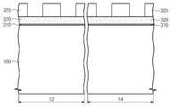
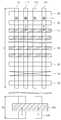
도 1은 본 발명의 실시예들에 따른 반도체 장치의 평면도이다. 도 2a는 본 발명의 제 1 실시예에 따른 반도체 장치를 설명하기 위한 것으로, 도 1의 A-A' 점선 및 B-B' 점선에 따른 단면도이다. 제 1 단면 영역(12)은 도 1의 A-A' 점선에 따른 단면 영역일 수 있다. 제 2 단면 영역(14)은 도 1의 B-B' 점선에 따른 단면 영역일 수 있다.1 is a plan view of a semiconductor device according to example embodiments. FIG. 2A is a cross-sectional view taken along line A-A 'and line B-B' of FIG. 1 to describe a semiconductor device according to a first embodiment of the present invention. The first
도 1 및 도 2a를 참조하면, 본 발명의 제 1 실시예에 따른 반도체 장치(500)는 가령, 낸드형 플래시 메모리 장치일 수 있다. 상기 반도체 장치(500)는 셀 영역(10)을 포함하는 기판(100)을 포함한다. 셀 영역(10)은 복수개의 셀 스트링들로 이루어진 셀 어레이를 포함한다. 셀 스트링은 접지 선택 라인(130), 스트링 선택 라인(120) 및 접지 선택 라인(130)과 스트링 선택 라인(120) 사이의 워드 라인들(125)을 포함한다. 공통 소오스 라인(140)이 서로 인접한 접지 선택 라인(130)들 사이에 제공된다. 공통 소오스 라인(140)은 접지 선택 라인(130)의 소오스 영역들(미도시)을 전기적으로 연결시킨다. 비트 라인 콘택(115)이 서로 인접한 스트링 선택 라인(120)들 사이에 제공된다. 비트 라인(360)이 워드 라인(125) 상에 배치된다.1 and 2A, the
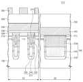
소자분리 구조체(270)가 기판(100)에서 활성 영역(110)을 정의한다. 소자분리 구조체(270)는 기판(100)으로부터 돌출될 수 있다. 터널 절연막(310) 및 전하 저장막(320)이 제 1 단면 영역(12)의 활성 영역(110) 상에 차례로 적층되어 있다. 전하 저장막(320)의 상면은 제 1 단면 영역(12)의 소자분리 구조체(270)의 상면 가령, 돌출면과 공면을 이룰 수 있다. 블록킹 절연막(330)이 제 1 단면 영역(12)의 소자분리 구조체(270) 상 및 전하 저장막(320) 상에 있다. 블록킹 절연막(330)은 제 1 단면 영역(12)의 소자분리 구조체(270)의 상면 및 전하 저장막(320)의 상면을 균일한 두께로 덮을 수 있다. 블록킹 절연막(330)은 제 2 단면 영역(14)의 소자분리 구조체(270)의 돌출부 및 활성 영역(110)을 균일한 두께로 덮을 수 있다. 워드 라인(125)을 구성하는 제어 게이트 전극(340)이 제 1 단면 영역(12)의 블록킹 절연 막(330)을 덮는다. 층간 절연막(350)이 제 1 단면 영역(12)의 제어 게이트 전극(320) 및 제 2 단면 영역(14)의 블록킹 절연막(330)을 덮을 수 있다. 비트 라인(360)이 층간 절연막(350) 상에 배치된다.An
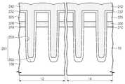
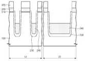
본 발명의 제 1 실시예에 따르면, 소자분리 구조체(270)는 제 1 절연 패턴(230), 제 2 절연 패턴(240) 및 에어 갭(air gap, 255)을 포함하는 제 3 절연 패턴(250)으로 구성될 수 있다. 소자분리 구조체(270)는 전하 저장막(320), 터널 절연막(310) 및 기판(100)의 일부를 관통하는 리세스 영역(200)를 채운다. 리세스 영역(200)는 측면(202) 및 바닥면(204)에 의해 정의될 수 있다. 리세스 영역(200)의 측면(202)은 전하 저장막(320)의 측면, 터널 절연막(310)의 측면 및 기판(100)에 형성된 트렌치의 측면과 공면을 이룰 수 있다. 리세스 영역(200)의 측면(202)은 수직하거나 정경사를 가질 수 있다. 리세스 영역(200)의 바닥면(204)은 상기 트렌치의 바닥면이다. 리세스 영역(200) 내에서 상기 측면(202) 사이의 거리는 제 1 폭(W1)일 수 있다. 제 1 폭(W1)은 가령, 20nm 내지 90nm 일 수 있다.According to the first embodiment of the present invention, the
제 1 절연 패턴(230)은 내벽(210) 및 바닥부(224)를 포함한다. 상기 바닥부(224)는 리세스 영역(200)의 바닥면(204)을 덮고, 상기 내벽(210)은 상기 바닥부(224)와 연결되며 상기 리세스 영역(200)의 측면(202) 일부를 따라 덮을 수 있다. 상기 내벽(210)은 제 3 절연 패턴(250)과 접하는 상면(211) 및 상기 상면(211)과 연결되며 상기 제 2 및 제 3 절연 패턴(240, 250)과 접하는 측면을 포함할 수 있다. 상기 내벽(210)의 상면(211)은 제 3 절연 패턴(250)의 상면과 이격될 수 있다. 상기 내벽(210)은 터널 절연막(310)의 측면을 덮을 수 있다. 상기 내벽(210)의 상면(211)은 제 1 범위에 위치할 수 있다. 제 1 범위는 제 1 거리 내 또는 제 2 거리 내일 수 있다. 제 1 거리는 기판(100)의 표면으로부터 상향으로 300Å 이하의 거리일 수 있다. 제 2 거리는 기판(100)의 표면으로부터 하향으로 500Å 이하의 거리일 수 있다. 상향은 기판(100)에서 수직으로 블록킹 절연막(330)을 향하는 방향이며, 하향은 상기 상향에 반대하는 방향일 수 있다. 내벽(210)의 두께는 상기 제 1 폭(W1)의 35% 이하 일 수 있다. 제 1 절연 패턴(230)은 제 2 절연 패턴(240) 및 제 3 절연 패턴(250)에 비해 유전 상수가 낮은 막을 포함할 수 있다. 제 1 절연 패턴(230)은 가령, 중온 산화막일 수 있다. 제 1 절연 패턴(230)은 다공성 박막으로 탄소 또는/및 수소를 포함한 실리콘 산화막을 포함할 수 있다.The first
제 2 절연 패턴(240)은 제 1 절연 패턴(230)의 바닥부(224)를 덮으며 평탄한 상면(242)을 가질 수 있다. 제 2 절연 패턴(240)의 상면(242)은 제 2 범위에 위치할 수 있다. 제 2 범위는 상기 기판(100)의 표면으로부터 상기 하향으로 500Å 이하의 거리일 수 있다. 제 2 절연 패턴(240)은 가령, 에스오지막(Spin On Glass layer: SOG layer), 유동성 산화막(flowable oxide layer: FOX layer), 비피에스지 막 (Boro-phospho Silicate Glass: BPSG layer) 또는 도펀트가 도핑된 산화막 가령, 게르마늄(Ge)이 도핑된 산화막 및 그 들의 조합 중에 선택된 어느 하나를 포함할 수 있다.The second
리세스 영역(200)는 제 1 영역(R1) 및 제 2 영역(R2)을 포함할 수 있다. 제 1 영역(R1)은 제 1 폭(W1)을 가질 수 있다. 제 1 폭(W1)은 리세스 영역(200)의 측면(202) 사이의 거리일 수 있다. 제 1 영역(R1)은 제 1 절연 패턴(230)의 내 벽(210)의 상면(211)과 제 3 절연 패턴(250)의 상면 사이의 영역을 포함할 수 있다. 제 2 영역(R2)은 제 2 폭(W2)을 가질 수 있다. 제 2 폭(W2)은 상기 내벽(210)의 측면 사이의 거리일 수 있다. 제 2 영역(R2)은 상기 내벽(210)의 상면(211)과 제 2 절연 패턴(240)의 상면(242) 사이의 영역을 포함할 수 있다.The
제 3 절연 패턴(250)은 리세스 영역(200)의 제 1 영역(R1) 및 제 2 영역(R2)에 채워져 있다. 에어 갭(255)은 제 2 영역(R2) 내에 배치되어 터널 절연막(310)에 인접한 활성 영역(110) 사이에 배치될 수 있다. 제 3 절연 패턴(250)은 가령, 고밀도 플라즈마(high density plasma: HDP) 산화막을 포함할 수 있다. The third
본 발명의 제 1 실시예에 따르면, 소자분리 구조체(270)는 유전 상수가 작은 에어 갭(255)을 포함하므로 작은 유전 상수를 가질 수 있다. 이에 따라, 활성 영역(110) 및 활성 영역(110)을 정의하는 소자분리 영역에 대한 임계 치수의 감소로 인한 채널 간의 간섭 현상(channel coupling)이 감소될 수 있다. 게다가, 본 발명의 제 1 실시예에 따르면, 소자분리 구조체(270)는 제 1 절연 패턴(230)의 내벽(210)의 상면(211)과 제 2 절연 패턴(240)의 상면(242)의 위치를 조절하여 균일하게 형성된 에어 갭(255)을 가질 수 있다. 에어 갭(255)은 터널 절연막(310)에 인접한 활성 영역(110) 사이에 배치될 수 있다. 이에 따라, 리세스 영역(200)에 형성된 소자분리 구조체(270)의 균일성을 열화시키지 않으며, 채널 간의 간섭 현상(channel coupling)이 보다 감소될 수 있다.According to the first embodiment of the present invention, since the
결과적으로, 채널 간의 간섭 현상이 저감됨에 따라, 낸드형 플래시 메모리 장치의 프로그램 시 비선택된 셀 트렌지스터의 채널에 걸리는 전압이 상승하여 채 널 부스팅 효율이 향상될 수 있다. 게다가, 상기 부스팅 시 채널 전압의 산포가 개선될 수 있다.As a result, as the interference between the channels is reduced, the voltage applied to the channel of the non-selected cell transistors during programming of the NAND flash memory device may increase, thereby improving channel boosting efficiency. In addition, the distribution of the channel voltage during the boosting can be improved.
도 2b는 본 발명의 제 2 실시예에 따른 반도체 장치를 설명하기 위한 것으로, 도 1의 A-A' 점선 및 B-B' 점선에 따른 단면도이다. 상기 제 2 실시예는 앞서 설명한 제 1 실시예와 유사하다. 따라서, 설명의 간결함을 위해, 아래에서는 앞서 설명한 제 1 실시예와 중복되는 기술적 특징에 대한 설명은 개략적으로 언급되거나 생략된다.FIG. 2B is a cross-sectional view taken along line A-A 'and line B-B' of FIG. 1 to describe a semiconductor device according to a second embodiment of the present invention. The second embodiment is similar to the first embodiment described above. Therefore, for the sake of brevity of description, the description of the technical features overlapping with the first embodiment described above will be outlined or omitted.
도 2b를 참조하면, 본 발명의 제 2 실시예에 따른 소자분리 구조체(271)는 제 1 절연 패턴(230), 제 2 절연 패턴(240), 에어 갭(256)을 포함하는 제 3 절연 패턴(251) 및 제 4 절연 패턴(260)으로 구성될 수 있다.Referring to FIG. 2B, the
제 4 절연 패턴(260)은 제 1 절연 패턴(230)의 내벽(210)의 상면(211) 및 상기 상면(211)과 연결되며 상기 상면(211)과 인접한 측면을 덮을 수 있다. 제 4 절연 패턴(260)은 제 1 영역과 제 2 영역의 경계에 배치될 수 있다. 제 4 절연 패턴(260)의 잔류물(미도시)은 제 2 절연 패턴(240) 상에 잔류할 수 있다. 제 4 절연 패턴(260)은 제 1 내지 제 3 절연 패턴들(230, 240, 250)에 비해 스텝 커버리지(step coverage)가 나쁜 막을 포함할 수 있다. 제 4 절연 패턴(260)는 가령, 플라즈마 강화 산화막(Plasma Enhanced oxide: PEOX)일 수 있다.The fourth
본 발명의 제 2 실시예에 따르면, 제 4 절연 패턴(260)을 더 포함하며 제 4 절연 패턴(260)에 의해 보다 용이하게 형성된 에어 갭(256)을 구비한 소자분리 구조체(271)을 포함하는 반도체 장치(501)를 제공할 수 있다. 에어 갭(256)의 형성 방 법은 후술한다.According to the second embodiment of the present invention, the
도 3a 내지 도 3j는 본 발명의 제 1 실시예에 따른 반도체 장치의 제조 방법을 설명하기 위한 단면도들이다. 제 1 단면 영역(12)은 도 1의 A-A' 점선에 따른 단면 영역일 수 있다. 제 2 단면 영역(14)은 도 1의 B-B' 점선에 따른 단면 영역일 수 있다.3A to 3J are cross-sectional views illustrating a method of manufacturing a semiconductor device in accordance with a first embodiment of the present invention. The first
도 1 및 도 3a를 참조하면, 제 1 단면 영역(12) 및 제 2 단면 영역(14)을 포함하는 기판(100)을 제공한다. 기판(100)은 가령, 실리콘 기판일 수 있다. 상기 기판(100) 상에 차례로 터널 절연막(310) 및 전하 저장막(320)을 형성한다. 터널 절연막(310)은 가령, 열 산화막을 포함할 수 있다. 전하 저장막(320)은 전하 트랩층 또는 부유 게이트일 수 있다. 상기 전하 트랩층은 실리콘 질화막, 나노 결정 실리콘(nano crystalline silicon), 나노 결정 실리콘게르마늄(nano crystalline silicon germanium), 나노 결정 금속(nano crystalline metal), 알루미늄 산화막, 하프늄 산화막, 하프늄알루미늄산화막 및 하프늄실리콘산화질화막을 구비하는 그룹에서 선택되는 적어도 하나를 포함할 수 있다.1 and 3A, a
전하 저장막(320) 상에 마스크막(325)을 형성한다. 상기 마스크막(325)은 패터닝된 막으로 전하 저장막(320)의 소정 영역을 노출할 수 있다. 상기 마스크막(325)은 가령, 실리콘 질화막을 포함할 수 있다.The
도 1 및 도 3b를 참조하면, 마스크막(325), 전하 저장막(320), 터널 절연막(310) 및 기판(100)의 일부를 관통하는 리세스 영역(201)을 형성한다. 예를 들면, 마스크막(325)을 식각 마스크로 사용하여 전하 저장막(320), 터널 절연막(310) 및 기판(100)의 일부를 이방성 식각하여 리세스 영역(201)을 형성할 수 있다. 식각 공정은 식각 대상에 따라 식각 가스를 달리하여 수행될 수 있다.1 and 3B, a
리세스 영역(201)는 내면인 측면(203) 및 바닥면(205)에 의해 정의될 수 있다. 리세스 영역(201)의 측면(203)은 마스크막(325)의 측면(203), 전하 저장막(320)의 측면, 터널 절연막(310)의 측면 및 반도체 기판(100)에 형성된 트렌치의 측면을 포함할 수 있다. 리세스 영역(201)의 측면(203)은 수직하거나 정경사를 가질 수 있다. 리세스 영역(201)의 바닥면(205)은 상기 트렌치의 바닥면이다. 리세스 영역(201) 내에서 상기 측면(203) 사이의 거리는 제 1 폭(W1)일 수 있다.The recessed
도 1 및 도 3c를 참조하면, 리세스 영역(201)의 내면을 따라 덮는 제 1 절연막(232)을 형성한다. 제 1 절연막(232)은 후속으로 형성될 제 2 절연막(242) 및 제 3 절연막(도 3g의 252)에 비해 유전 상수가 낮은 막으로 형성될 수 있다. 제 1 절연막(232)은 가령, 중온 산화막으로 형성될 수 있다. 제 1 절연막(232)은 다공성 박막으로 탄소 또는/및 수소를 포함한 실리콘 산화막을 포함할 수 있다.1 and 3C, a first insulating
제 1 절연막(232) 상에 절연 물질을 형성하여 리세스 영역(201)을 채우는 제 2 절연막(242)을 형성한다. 제 2 절연막(242)은 제 1 절연막(232), 전하 저장막(320) 및 마스크막(325)에 대하여 습식 식각 선택비를 갖는 막일 수 있다. 제 2 절연막(242)은 가령, 제 1 절연막(232)에 비해 3 배 이상 빠르게 습식 식각되는 막을 포함할 수 있다. 제 2 절연막(242)은 좁은 폭을 갖는 영역에서 빠르게 습식 식각되는 성질을 갖는 막일 수 있다. 제 2 절연막(242)은 가령, 에스오지막(Spin On Glass layer: SOG layer), 유동성 산화막(flowable oxide layer: FOX layer), 비피 에스지 막 (Boro-phospho Silicate Glass: BPSG layer), 도펀트가 도핑된 산화막 가령, 게르마늄(Ge)이 도핑된 산화막 및 그들의 조합 중에 선택된 어느 하나로 형성될 수 있다.An insulating material is formed on the first insulating
도 1 및 도 3d를 참조하면, 제 2 절연막(도 3c의 242) 및 제 1 절연막(232)을 마스크막(325)이 노출될 때까지 평탄화하여 평탄화된 제 2 절연막(244) 및 평탄화된 제 1 절연막(234)을 형성한다. 평탄화 공정은 가령, 화학 기계적 연마 공정을 포함할 수 있다.1 and 3D, the second
상기 평탄화 공정에 의해, 평탄화된 제 2 절연막(244)의 상면과 및 평탄화된 제 1 절연막(234)의 내벽(214)의 상면은 마스크막(325)의 상면과 공면을 이룰 수 있다. 상기 평탄화된 제 1 절연막(234)은 내벽(214) 및 바닥부(225)를 포함한다. 상기 바닥부(225)는 리세스 영역(201)의 바닥면(205)을 덮는다. 상기 내벽(214)는 상기 바닥부(225)와 연결되며 리세스 영역(201)의 측면(203)을 따라 덮을 수 있다. 후속으로 형성될 에어 갭(air gap, 도 3g의 255)이 차지할 공간을 고려하여, 상기 내벽(214)의 두께(T)는 가령, 리세스 영역(201)의 제 1 폭(W1)의 35% 이하로 형성될 수 있다. 리세스 영역(201) 내에서 상기 내벽(214) 사이의 거리는 제 2 폭(W2)이라 정의할 수 있다.By the planarization process, an upper surface of the planarized second insulating
상기 평탄화된 제 2 절연막(244)의 습식 식각 선택비를 높이기 위해, 제 2 절연막(도 3c의 242)의 형성 후 또는 상기 평탄화 공정 후에 열처리 공정이 추가될 수 있다. 열처리 공정은 가령, 자외선 어닐 공정(UV anneal process)을 포함할 수 있다.In order to increase the wet etching selectivity of the planarized second insulating
도 1 및 도 3e를 참조하면, 마스크막(325) 사이에 상기 평탄화된 제 2 절연막(도 3d의 244) 및 평탄화된 제 1 절연막(234)을 제 1 리세스하여, 리세스 영역(201)에 제 1 폭(W1)을 갖는 제 1 영역(R1)을 제공한다. 예를 들면, 마스크막(325)을 식각 마스크로 사용하여 상기 평탄화된 제 2 절연막(도 3d의 244) 및 상기 평탄화된 제 1 절연막(도 3d의 234)의 내벽(214)을 이방성 식각하여 리세스 영역(201)의 측면(203)을 노출할 수 있다. 이에 따라, 리세스 영역(201)에 상기 노출된 측면(203) 사이의 거리인 제 1 폭(W1)을 갖는 제 1 영역(R1)을 제공할 수 있다.1 and 3E, the planarized second insulating film 244 (FIG. 3D) and the planarized first insulating
상기 제 1 리세스 공정에 의해, 마스크막(325) 사이에 제 1 리세스된 제 1 절연 패턴(230) 및 제 1 리세스된 예비 제 2 절연 패턴(246)이 형성된다. 상기 제 1 절연 패턴(230)의 내벽(210)의 상면(211)이 제 1 범위에 위치하도록 제 1 리세스 공정이 수행될 수 있다. 제 1 범위는 제 1 거리 내 또는 제 2 거리 내일 수 있다. 제 1 거리는 기판(100)의 표면으로부터 상향으로 300Å 이하의 거리일 수 있다. 제 2 거리는 기판(100)의 표면으로부터 하향으로 500Å 이하의 거리일 수 있다. 상향은 기판(100)에서 마스크막(325)으로 향하는 방향이며, 하향은 상기 상향에 반대하는 방향일 수 있다. 터널 절연막(310)의 보호를 위해, 제 1 리세스 공정은 터널 절연막(310)의 측면이 노출되기 전까지 진행될 수 있다.By the first recess process, a first recessed first
도 1 및 도 3f를 참조하면, 제 1 절연 패턴(230)의 내벽(210) 사이에 상기 예비 제 2 절연 패턴(도 3e의 246)을 제 2 리세스하여, 리세스 영역(201)에 상기 제 2 폭(W2)을 갖는 제 2 영역(R2)을 제공한다. 예를 들면, 상기 예비 제 2 절연 패턴(도 3e의 246)을 선택적으로 습식 식각하여, 제 1 절연 패턴(230)의 내벽(210) 의 측면 일부를 노출할 수 있다. 이에 따라, 리세스 영역(201)에 상기 노출된 내벽(210)의 측면 사이의 거리인 제 2 폭(W2)을 갖는 제 2 영역(R2)을 제공할 수 있다. 1 and 3F, the preliminary second
제 2 리세스 공정에 의해, 상기 예비 제 2 절연 패턴(도 3e의 246)은 제 2 절연 패턴(240)으로 형성된다. 제 2 절연 패턴(240)은 제 1 절연 패턴(230)의 바닥부(224)을 덮으며 상기 내벽(210) 하부의 측면 사이에 형성될 수 있다. 제 2 절연 패턴(240)은 평탄한 상면을 가질 수 있다. 제 2 리세스 공정은 제 2 절연 패턴(240)의 상면(242)이 제 2 범위에 위치할 때까지 진행될 수 있다. 제 2 범위는 기판(100)의 표면으로부터 상기 하향으로 500Å 이하의 거리 내일 수 있다.By the second recess process, the preliminary second
도 1 및 도 3g를 참조하면, 제 1 영역(도 3f의 R1) 및 제 2 영역(R2)을 갖는 리세스 영역(201)을 절연물질로 채워 에어 갭(255)을 갖는 제 3 절연막(252)을 형성한다. 제 3 절연막(252)은 가령, 고밀도 플라즈마(high density plasma: HDP) 산화막으로 형성할 수 있다. 리세스 영역(201)에서 제 1 영역(R1)의 폭이 상기 제 2 영역(R2)의 폭보다 크다. 따라서, 리세스 영역(201)에 절연물질을 채울 때 제 2 영역(R2)의 입구에 오버행에 의한 에어 갭(255)이 제 2 영역(R2) 내에 형성될 수 있다.1 and 3G, a third
본 발명의 제 1 실시예에 따르면, 제 2 절연 패턴(240)의 상면(242)의 위치와 제 1 절연 패턴(230)의 내벽(210)의 상면(211)의 위치를 조절할 수 있다. 이에 따라, 리세스 영역(201) 내에 에어 갭(255)의 위치가 설정될 수 있고, 에어 갭(255)이 균일하게 형성될 수 있다. 게다가, 에어 갭(255)은 터널 절연막(310)과 인접한 활성 영역(110) 사이에 형성될 수 있다.According to the first embodiment of the present invention, the position of the
도 1 및 도 3h를 참조하면, 제 3 절연막(도 3g의 252) 및 마스크막(325)을 전하 저장막(320)이 노출될 때까지 평탄화하여 제 3 절연 패턴(250)을 형성할 수 있다. 평탄화 공정은 화학 기계적 연마 공정을 포함할 수 있다. 제 1 절연 패턴(230), 제 2 절연 패턴(240) 및 제 3 절연 패턴(250)은 소자분리 구조체(270)를 구성할 수 있다. 상기 평탄화 공정에 의해, 제 3 절연 패턴(250)의 상면과 전하 저장막(320)의 상면은 공면을 이룰 수 있다.1 and 3H, the third insulating layer 250 (252 of FIG. 3G) and the
상기 평탄화 공정 후, 제 1 단면 영역(12)을 마스킹하고, 제 2 단면 영역(14)의 전하 저장막(320) 및 터널 절연막(310)을 선택적으로 제거하여 소자분리 구조체(270) 사이의 기판(100)을 노출시킬 수 있다. 상기 제거 공정은 가령, 이방성 식각 공정일 수 있다.After the planarization process, the first
도 1 및 도 3i를 참조하면, 제 1 단면 영역(12)의 제 3 절연 패턴(250) 및 전하 저장막(320)과 제 2 단면 영역(14)의 소자분리 구조체(270) 및 노출된 기판(100)을 덮는 블록킹 절연막(330)을 형성할 수 있다. 블록킹 절연막(330)은 가령, 화학 기상 증착 공정을 수행하여 균일한 두께로 형성될 수 있다. 블록킹 절연막(330)은 고유전막으로서 SiO2, SiN, SiON, HfO2, ZrO2, Al2O3 또는 이들의 조합으로 형성될 수 있다.1 and 3I, the
제 1 단면 영역(12)의 블록킹 절연막(330) 상에 제어 게이트 전극(340)을 형성한다. 예를 들면, 제 1 단면 영역(12) 및 제 2 단면 영역(14)의 블록킹 절연 막(330) 상에 도전막을 형성하고, 도전막을 패터닝하여 제어 게이트 전극(340)을 형성할 수 있다. 상기 패터닝 공정은 상기 도전막을 제 2 단면 영역(14)의 블록킹 절연막(330)을 노출할 때까지 이방성 식각하는 공정을 포함할 수 있다. 본 발명의 제 1 실시예에 따르면, 블록킹 절연막(330)을 식각 정지막으로 사용하여 상기 식각 공정에 의해 발생할 수 있는 과식각으로 인한 제 2 단면 영역(14)의 소자 분리막 구조체(260)의 에어 갭(255)의 노출을 방지할 수 있다.The
도 1 및 도 3j를 참조하면, 제 1 단면 영역(12)의 제어 게이트 전극(340) 및 제 2 단면 영역(14)의 블록킹 절연막(330)을 덮는 층간 절연막(350)을 형성한다. 층간 절연막(350) 상에 비트 라인(360)을 형성한다.1 and 3J, an
도 4a 내지 도 4c는 본 발명의 제 2 실시예에 따른 반도체 장치의 제조 방법을 설명하기 위한 단면도들이다. 상기 제 2 실시예는 앞서 설명한 제 1 실시예와 유사하다. 따라서, 설명의 간결함을 위해, 아래에서는 앞서 설명한 제 1 실시예와 중복되는 기술적 특징에 대한 설명은 개략적으로 언급되거나 생략된다.4A to 4C are cross-sectional views illustrating a method of manufacturing a semiconductor device in accordance with a second embodiment of the present invention. The second embodiment is similar to the first embodiment described above. Therefore, for the sake of brevity of description, the description of the technical features overlapping with the first embodiment described above will be outlined or omitted.
도 4a를 참조하면, 도 1과 도 3a 내지 도 3f의 방법으로 제 1 절연 패턴(230)의 내벽(210) 사이에 제 2 절연 패턴(240)을 형성할 수 있다.Referring to FIG. 4A, a second
제 1 절연 패턴(230)의 내벽(210)의 상면(211) 및 상기 상면(211)과 연결되며 상기 상면(211)과 인접한 측면을 덮는 제 4 절연 패턴(260)을 형성할 수 있다. 제 4 절연 패턴(260)의 잔류물(미도시)은 제 2 절연 패턴(240) 상에 형성될 수 있다. 제 4 절연 패턴(260)는 제 1 내지 제 3 절연 패턴들(230, 240, 250)에 비해 스텝 커버리지(step coverage)가 나쁜 막으로 형성될 수 있다. 제 4 절연 패턴(260)는 가령, 플라즈마 강화 산화막(Plasma Enhanced oxide: PEOX)으로 형성될 수 있다.A fourth
도 4b를 참조하면, 리세스 영역(201)을 절연물질로 채워 에어 갭(256)을 형성할 수 있다. 본 발명의 제 2 실시예에 따르면, 리세스 영역(201)의 제 1 영역과 제 2 영역의 경계에 제 4 절연 패턴(260)을 형성하여, 리세스 영역(201)에 절연물질을 채울 때 제 2 영역의 입구에 오버행이 가중될 수 있어, 에어 갭(256)의 형성이 보다 용이할 수 있다.Referring to FIG. 4B, an
상기 에어 갭(256)을 형성한 후, 상기 절연물질 및 마스크막(325)을 전하 저장막(320)이 노출될 때까지 평탄화하여, 제 1 단면 영역(12) 및 제 2 단면 영역(14)에 제 3 절연 패턴(251)을 형성할 수 있다. 제 1 절연 패턴(230), 제 2 절연 패턴(240), 에어 갭(256)을 포함하는 제 3 절연 패턴(251) 및 제 4 절연 패턴(260)은 본 발명의 제 2 실시예에 따른 소자분리 구조체(271)를 구성할 수 있다.After the
상기 평탄화 공정 후, 제 1 단면 영역(12)을 마스킹하고 제 2 단면 영역(14)의 전하 저장막(도 4a의 320) 및 터널 절연막(310)을 선택적으로 제거하여 소자분리 구조체(270) 사이의 기판(100)을 노출시킬 수 있다. 상기 제거 공정은 가령, 이방성 식각 공정일 수 있다.After the planarization process, the first
도 4c를 참조하면, 도 1과 도 3i 내지 도 3j의 방법으로 블록킹 절연막(330), 제어 게이트 전극(340), 층간 절연막(350) 및 비트 라인(360)을 형성할 수 있다.Referring to FIG. 4C, the blocking insulating
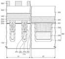
도 5은 본 발명의 변형 실시예에 따른 반도체 장치의 평면도이다. 도 6은 본 발명의 변형 실시예에 따른 반도체 장치를 설명하기 위한 것으로, 도 5의 A-A' 점선 및 C-C' 점선에 따른 단면도이다. 상기 변형 실시예는 앞서 설명한 제 1 실시예 와 유사하다. 따라서, 설명의 간결함을 위해, 아래에서는 앞서 설명한 제 1 실시예와 중복되는 기술적 특징에 대한 설명은 개략적으로 언급되거나 생략된다. 제 3 단면 영역(14)은 도 1의 C-C' 점선에 따른 단면 영역일 수 있다.5 is a plan view of a semiconductor device according to a modified embodiment of the present invention. FIG. 6 is a cross-sectional view taken along line A-A 'and line C-C' of FIG. 5 to describe a semiconductor device according to an exemplary embodiment of the present invention. The modified embodiment is similar to the first embodiment described above. Therefore, for the sake of brevity of description, the description of the technical features overlapping with the first embodiment described above will be outlined or omitted. The third
도 5 및 도 6을 참조하면, 셀 영역(10) 및 회로 영역(20)을 포함하는 기판(100)이 있다. 셀 영역(10)은 셀 영역(10)은 복수개의 셀 스트링들로 이루어진 셀 어레이를 포함한다. 셀 스트링은 접지 선택 라인(130), 스트링 선택 라인(120) 및 접지 선택 라인(130)과 스트링 선택 라인(120) 사이의 워드 라인들(125)을 포함한다. 공통 소오스 라인(140)이 서로 인접한 접지 선택 라인(130)들 사이에 제공된다. 공통 소오스 라인(140)은 접지 선택 라인(130)의 소오스 영역들(미도시)을 전기적으로 연결시킨다. 비트 라인 콘택(115)이 서로 인접한 스트링 선택 라인(120)들 사이에 제공된다. 비트 라인(360)이 워드 라인(125) 상에 배치된다. 5 and 6, there is a
셀 영역(10)의 소자분리 구조체(274)가 기판(100)에서 활성 영역(110)을 정의한다. 상기 소자분리 구조체(274)는 제 1 절연 패턴(230), 제 2 절연 패턴(240) 및 에어 갭(255)을 포함하는 제 3 절연 패턴(250)으로 구성될 수 있다. 터널 절연막(310) 및 전하 저장막(320)이 상기 활성 영역(110) 상에 차례로 적층되어 있다. 블록킹 절연막(330)이 소자분리 구조체(274) 상 및 전하 저장막(320) 상에 있다. 블록킹 절연막(330)은 소자분리 구조체(274)의 상면 및 전하 저장막(320)의 상면을 균일한 두께로 덮을 수 있다. 워드 라인(125)을 구성하는 제어 게이트 전극(340)이 제 1 단면 영역(12)의 블록킹 절연막(330)을 덮는다. 층간 절연막(350)이 제 1 단면 영역(12)의 제어 게이트 전극(320)을 덮을 수 있다. 비트 라인(360)이 층간 절 연막(350) 상에 배치된다.An
회로 영역(20)은 게이트 전극(345), 게이트 절연막(312) 및 게이트 전극(345)의 양측의 회로 활성 영역(290)에 형성된 소오스/드레인 영역(미도시)을 포함하는 고전압 및/또는 저전압 트랜지스터를 포함한다. 회로 소자분리 구조체(280)가 회로 영역(20)의 기판(100)에 회로 활성 영역(290)을 정의한다. 게이트 전극(345)은 게이트 절연막(312)의 개재 하에 회로 활성 영역(290) 상에 있다. 게이트 전극(345)은 제 3 단면 영역(22)의 회로 소자분리 구조체(280) 상에 있을 수 있다. 층간 절연막(350)이 제 3 단면 영역(22)의 게이트 전극(345)을 덮는다.The
본 발명의 변형예에 따른 회로 소자분리 구조체(280)는 셀 영역(10)에 형성된 소자분리 구조체(274)와 동일 또는 유사한 물질로, 제 3 단면 영역(22)에 배치되는 제 1 절연 패턴(230), 제 2 절연 패턴(240) 및 주변 제 3 절연 패턴(254)으로 구성될 수 있다. 주변 제 3 절연 패턴(254)은 셀 영역(10)의 제 3 절연 패턴(250)과 동일 또는 유사한 물질을 포함할 수 있다. 본 발명의 변형예에 따르면, 소자분리 구조체(274) 및 주변 소자분리 구조체(280)를 포함하는 반도체 장치(510)를 제공할 수 있다.The
도 7a 내지 도 7d는 본 발명의 변형 실시예에 따른 반도체 장치의 제조 방법을 설명하기 위한 단면도들이다. 상기 변형 실시예는 앞서 설명한 제 1 실시예와 유사하다. 따라서, 설명의 간결함을 위해, 아래에서는 앞서 설명한 제 1 실시예와 중복되는 기술적 특징에 대한 설명은 개략적으로 언급되거나 생략된다.7A to 7D are cross-sectional views illustrating a method of manufacturing a semiconductor device in accordance with a modified embodiment of the present invention. The modified embodiment is similar to the first embodiment described above. Therefore, for the sake of brevity of description, the description of the technical features overlapping with the first embodiment described above will be outlined or omitted.
도 7a를 참조하면, 도 1 및 도 3e의 방법으로 제 1 리세스 공정을 수행하여 제 1 단면 영역(12)의 마스크막(325) 사이에 제 1 리세스된 제 1 절연 패턴(230) 및 제 1 리세스된 예비 제 2 절연 패턴(246)을 형성할 수 있다.Referring to FIG. 7A, the first
상기 제 1 리세스 공정에 의해, 제 3 단면 영역(22)의 마스크막(325) 사이에 제 1 리세스된 제 1 절연 패턴(230) 및 제 1 리세스된 예비 제 2 절연 패턴(246)을 형성할 수 있다.By the first recess process, a first recessed first
도 7b를 참조하면, 제 1 단면 영역(12)의 예비 제 2 절연 패턴(도 7a의 246)을 선택적으로 제 2 리세스하여, 제 1 절연 패턴(230)의 내벽 사이에 제 2 절연 패턴(240)을 형성할 수 있다.Referring to FIG. 7B, the second preliminary second
상기 제 2 리세스 공정에 의해, 제 3 단면 영역(22)의 제 1 절연 패턴(230)의 내벽 사이에 제 2 절연 패턴(240)을 형성할 수 있다.By the second recess process, a second
도 7c를 참조하면, 제 1 단면 영역(12)의 리세스 영역(201)을 절연물질로 채워 에어 갭(255)을 형성할 수 있다. 상기 절연물질로 제 3 단면 영역(22)의 주변회로 트렌치(285)를 채울 수 있다. 주변회로 트렌치(285)의 폭이 리세스 영역(201)의 폭보다 크므로 주변회로 트렌치(285)에 에어 갭(255)이 형성되지 않을 수 있다.Referring to FIG. 7C, an
상기 에어 갭(255)을 형성한 후, 상기 절연물질 및 마스크막(325)을 전하 저장막(320)이 노출될 때까지 평탄화하여 제 1 단면 영역(12)의 전하 저장막(320) 사이에 제 3 절연 패턴(250)을 형성할 수 있다. 제 1 단면 영역(12)의 소자분리 구조체(274)는 제 1 절연 패턴(230), 제 2 절연 패턴(240) 및 에어 갭(255)을 포함하는 제 3 절연 패턴(250)으로 구성될 수 있다. 상기 평탄화 공정에 의해, 제 3 단면 영역(22)의 전하 저장막(도 7b의 320) 사이에 예비 제 3 절연 패턴을 형성할 수 있 다.After the
상기 평탄화 공정 후, 제 1 단면 영역(12) 상의 제 3 절연 패턴(250) 및 전하 저장막(320)을 마스킹하고, 제 3 단면 영역(22) 상의 예비 제 3 절연 패턴 및 전하 저장막(도 7b의 320)을 터널 절연막(310)이 노출될 때까지 평탄화하여 주변 제 3 절연 패턴(254)를 형성할 수 있다. 회로 소자분리 구조체(280)은 제 3 단면 영역(22) 상의 제 1 절연 패턴(230), 제 2 절연 패턴(240) 및 주변 제 3 절연 패턴(254)으로 형성될 수 있다. 제 3 단면 영역(22) 상의 터널 절연막(310)이 제거될 수 있다.After the planarization process, the third
도 7d를 참조하면, 제 1 단면 영역(12)의 소자분리 구조체(270) 상 및 전하 저장막(320) 상에 차례로 블록킹 절연막(330) 및 제어 게이트 전극(340)을 형성할 수 있다. 상기 제어 게이트 전극(340) 상에 차례로 층간 절연막(350) 및 비트 라인(360)을 형성할 수 있다.Referring to FIG. 7D, the blocking insulating
제 3 단면 영역(22)의 회로 활성 영역(290) 상 및 회로 소자분리 구조체(280) 상에 차례로 게이트 절연막(312) 및 게이트 전극(345)을 형성할 수 있다. 게이트 전극(345) 상에 층간 절연막(350)을 형성할 수 있다. 게이트 절연막(312)은 상기 블록킹 절연막(330)과 동일 또는 유사한 물질로 형성될 수 있다. 게이트 전극(345)은 제어 게이트 전극(340)과 동일 또는 유사한 물질로 형성될 수 있다.The
도 8는 본 발명의 실시예들에 따른 반도체 장치를 포함하는 전자 시스템을 나타내는 블럭도이다.8 is a block diagram illustrating an electronic system including a semiconductor device according to example embodiments.
도 8을 참조하면, 본 발명의 실시예들에 따른 전자 시스템(1000)은 제어 기(1410), 입출력 장치(1420) 및 기억 장치(1430)를 포함할 수 있다. 상기 제어기(1410), 입출력 장치(1420) 및 기억 장치(1430)는 버스(450, bus)를 통하여 서로 커플링(coupling)될 수 있다. 상기 버스(450)는 데이터들 및/또는 동작 신호들이 이동하는 통로에 해당한다. 상기 제어기(1410)는 적어도 하나의 마이크로프로세서, 디지털 신호 프로세서, 마이크로컨트롤러, 및 이들과 유사한 기능을 수행할 수 있는 논리 소자들 중에서 적어도 하나를 포함할 수 있다. 상기 입출력 장치(1420)는 키패드, 키보드 및 표시 장치(display device)등에서 선택된 적어도 하나를 포함할 수 있다. 상기 기억 장치(1430)는 데이터를 저장하는 장치이다. 상기 기억 장치(1430)는 데이터 및/또는 상기 제어기(1410)에 의해 실행되는 명령어 등을 저장할 수 있다. 상기 기억 장치(1430)는 상술한 실시예들에 따른 반도체 메모리 장치(500, 501, 510)를 포함할 수 있다. 상기 전자 시스템(1000)은 통신 네트워크로 데이터를 전송하거나 통신 네트워크로부터 데이터를 수신하기 위한 인터페이스(440)를 더 포함할 수 있다. 상기 인터페이스(440)는 유선 또는 무선 형태일 수 있다. 예컨대, 상기 인터페이스(440)는 안테나 또는 유무선 트랜시버등을 포함할 수 있다.Referring to FIG. 8, an
상기 전자 시스템(1000)은 모바일 시스템, 개인용 컴퓨터, 산업용 컴퓨터 또는 다양한 기능을 수행하는 시스템 등으로 구현될 수 있다. 예컨대, 상기 모바일 시스템은 개인 휴대용 정보 단말기(PDA; Personal Digital Assistant), 휴대용 컴퓨터, 웹 타블렛(web tablet), 모바일폰(mobile phone), 무선폰(wireless phone), 랩톱(laptop) 컴퓨터, 메모리 카드, 디지털 뮤직 시스템(digital music system) 또 는 정보 전송/수신 시스템 등일 수 있다. 상기 전자 시스템(1000)이 무선 통신을 수행할 수 있는 장비인 경우에, 상기 전자 시스템(1000)은 CDMA, GSM, NADC, E-TDMA, WCDAM, CDMA2000 같은 3세대 통신 시스템 같은 통신 인터페이스 프로토콜에서 사용될 수 있다.The
도 9는 본 발명의 실시예들에 따른 반도체 장치를 포함하는 메모리 카드를 나타내는 블럭도이다.9 is a block diagram illustrating a memory card including a semiconductor device according to example embodiments.
도 9를 참조하면, 본 발명의 실시예들에 따른 메모리 카드(2000)는 기억 장치(1510) 및 메모리 제어기(1520)를 포함한다. 상기 기억 장치(1510)는 데이터를 저장할 수 있다. 상기 기억 장치(1510)는 전원 공급이 중단될지라도 저장된 데이터를 그대로 유지하는 비휘발성 특성을 갖는 것이 바람직하다. 상기 기억 장치(1510)는 상술한 실시예들 또는 변형 실시예에 따른 반도체 메모리 장치(500, 501, 510)를 포함할 수 있다. 상기 메모리 제어기(1520)는 호스트(host)의 판독/쓰기 요청에 응답하여 상기 기억 장치(1510)에 저장된 데이터를 독출하거나, 상기 기억 장치(1510)에 데이터를 저장할 수 있다.9, a
상술한 실시예들에 따른 반도체 메모리 장치(500, 501, 510)는 다양한 형태의 패키지로 실장될 수 있다. 예를 들면, 상기 반도체 메모리 장치(500, 501, 510)는 패키지 온 패키지(Package on Package), 볼 그리드 어레이(Ball Grid Arrays), 칩 스케일 패키지(Chip scale packages), 플라스틱 리드 칩 캐리어(Plastic Leaded Chip Carrier), 플라스틱 듀얼 인라인 패키지(Plastic Dual In-Line Package), 멀티 칩 패키지(Multi Chip Package), 웨이퍼 레벨 패키지(Wafer Level Package), 웨 이퍼 레벨 제조 패키지(Wafer Level Fabricated Package), 웨이퍼 레벨 프로세스 스택 패키지(Wafer Level Processed Stack Package), 다이 온 와플 패키지(Die On Waffle Package), 다이 인 웨이퍼 폼(Die in Wafer Form), 칩 온 보오드(Chip On Board), 세라믹 듀얼 인라인 패키지(Ceramic Dual In-Line Package), 플라스킥 메트릭 쿼드 플랫 패키지(Plastic Metric Quad Flat Pack), 씬 쿼드 플랫 패키지(Thin Quad Flat Pack), 스몰 아웃라인 패키지(Small Outline Package), 축소 스몰 아웃라인 패키지(Shrink Small Outline Package), 씬 스몰 아웃라인 패키지(Thin Small Outline Package), 씬 쿼드 플랫 패키지(Thin Quad Flat Package), 시스템 인 패키지(System In Package) 등과 같은 방식으로 패키징될 수 있다.The
상기한 실시예들의 설명은 본 발명의 더욱 철저한 이해를 준비하기 위하여 도면을 참조로 예를 든 것에 불과하므로, 본 발명을 한정하는 의미로 해석되어서는 안될 것이다. 그리고, 본 발명의 기술분야에서 통상의 지식을 가진 자에게 본 발명의 기본적 원리를 벗어나지 않는 범위 내에서 다양한 변화와 변경이 가능함은 물론이다.The description of the above embodiments is only given by way of example with reference to the drawings in order to prepare a more thorough understanding of the present invention, and should not be construed as limiting the present invention. In addition, various changes and modifications are possible to those skilled in the art without departing from the basic principles of the present invention.
도 1은 본 발명의 실시예들에 따른 반도체 장치의 평면도이다.1 is a plan view of a semiconductor device according to example embodiments.
도 2a는 본 발명의 제 1 실시예에 따른 반도체 장치를 설명하기 위한 것으로, 도 1의 A-A' 점선 및 B-B' 점선에 따른 단면도이다.FIG. 2A is a cross-sectional view taken along line A-A 'and line B-B' of FIG. 1 to describe a semiconductor device according to a first embodiment of the present invention.
도 2b는 본 발명의 제 2 실시예에 따른 반도체 장치를 설명하기 위한 것으로, 도 1의 A-A' 점선 및 B-B' 점선에 따른 단면도이다.FIG. 2B is a cross-sectional view taken along line A-A 'and line B-B' of FIG. 1 to describe a semiconductor device according to a second embodiment of the present invention.
도 3a 내지 도 3j는 본 발명의 제 1 실시예에 따른 반도체 장치의 제조 방법을 설명하기 위한 단면도들이다.3A to 3J are cross-sectional views illustrating a method of manufacturing a semiconductor device in accordance with a first embodiment of the present invention.
도 4a 내지 도 4c는 본 발명의 제 2 실시예에 따른 반도체 장치의 제조 방법을 설명하기 위한 단면도들이다.4A to 4C are cross-sectional views illustrating a method of manufacturing a semiconductor device in accordance with a second embodiment of the present invention.
도 5은 본 발명의 변형 실시예에 따른 반도체 장치의 평면도이다.5 is a plan view of a semiconductor device according to a modified embodiment of the present invention.
도 6은 본 발명의 변형 실시예에 따른 반도체 장치를 설명하기 위한 것으로, 도 5의 A-A' 점선 및 C-C' 점선에 따른 단면도이다.FIG. 6 is a cross-sectional view taken along line A-A 'and line C-C' of FIG. 5 to describe a semiconductor device according to an exemplary embodiment of the present invention.
도 7a 내지 도 7d는 본 발명의 변형 실시예에 따른 반도체 장치의 제조 방법을 설명하기 위한 단면도들이다.7A to 7D are cross-sectional views illustrating a method of manufacturing a semiconductor device in accordance with a modified embodiment of the present invention.
도 8는 본 발명의 실시예들에 따른 반도체 장치를 포함하는 전자 시스템을 나타내는 블럭도이다.8 is a block diagram illustrating an electronic system including a semiconductor device according to example embodiments.
도 9는 본 발명의 실시예들에 따른 반도체 장치를 포함하는 메모리 카드를 나타내는 블럭도이다.9 is a block diagram illustrating a memory card including a semiconductor device according to example embodiments.
Claims (10)
Translated fromKoreanPriority Applications (2)
| Application Number | Priority Date | Filing Date | Title |
|---|---|---|---|
| KR1020090021321AKR20100102982A (en) | 2009-03-12 | 2009-03-12 | Semiconductor device |
| US12/711,033US20100230741A1 (en) | 2009-03-12 | 2010-02-23 | Semiconductor devices with an air gap in trench isolation dielectric |
Applications Claiming Priority (1)
| Application Number | Priority Date | Filing Date | Title |
|---|---|---|---|
| KR1020090021321AKR20100102982A (en) | 2009-03-12 | 2009-03-12 | Semiconductor device |
Publications (1)
| Publication Number | Publication Date |
|---|---|
| KR20100102982Atrue KR20100102982A (en) | 2010-09-27 |
Family
ID=42729972
Family Applications (1)
| Application Number | Title | Priority Date | Filing Date |
|---|---|---|---|
| KR1020090021321AWithdrawnKR20100102982A (en) | 2009-03-12 | 2009-03-12 | Semiconductor device |
Country Status (2)
| Country | Link |
|---|---|
| US (1) | US20100230741A1 (en) |
| KR (1) | KR20100102982A (en) |
Cited By (4)
| Publication number | Priority date | Publication date | Assignee | Title |
|---|---|---|---|---|
| KR20120051958A (en)* | 2010-11-15 | 2012-05-23 | 삼성전자주식회사 | Fabricating method of non volatile memory device and non volatile memory device thereby |
| KR20140071786A (en)* | 2012-12-04 | 2014-06-12 | 삼성전자주식회사 | Semiconductor memory device and method for fabricating the same |
| KR20170018165A (en)* | 2015-08-06 | 2017-02-16 | 삼성전자주식회사 | Semiconductor device |
| US10395972B2 (en) | 2013-03-29 | 2019-08-27 | Magnachip Semiconductor, Ltd. | Semiconductor device and manufacturing method thereof |
Families Citing this family (50)
| Publication number | Priority date | Publication date | Assignee | Title |
|---|---|---|---|---|
| JP2008283095A (en)* | 2007-05-14 | 2008-11-20 | Toshiba Corp | Nonvolatile semiconductor memory device and manufacturing method thereof |
| US8546239B2 (en)* | 2010-06-11 | 2013-10-01 | Sandisk Technologies Inc. | Methods of fabricating non-volatile memory with air gaps |
| US8946048B2 (en) | 2010-06-19 | 2015-02-03 | Sandisk Technologies Inc. | Method of fabricating non-volatile memory with flat cell structures and air gap isolation |
| US8603890B2 (en) | 2010-06-19 | 2013-12-10 | Sandisk Technologies Inc. | Air gap isolation in non-volatile memory |
| US8492224B2 (en) | 2010-06-20 | 2013-07-23 | Sandisk Technologies Inc. | Metal control gate structures and air gap isolation in non-volatile memory |
| KR20120015178A (en)* | 2010-08-11 | 2012-02-21 | 삼성전자주식회사 | Semiconductor device and semiconductor device manufacturing method |
| KR101559345B1 (en)* | 2010-08-26 | 2015-10-15 | 삼성전자주식회사 | Non volatile memory device and method for manufacturing the same |
| KR20120043979A (en)* | 2010-10-27 | 2012-05-07 | 삼성전자주식회사 | A non-volatile memory device and a method of forming the same |
| SG181212A1 (en)* | 2010-11-18 | 2012-06-28 | Toshiba Kk | Nonvolatile semiconductor memory and method of manufacturing with multiple air gaps |
| JP5570953B2 (en)* | 2010-11-18 | 2014-08-13 | 株式会社東芝 | Nonvolatile semiconductor memory device and method of manufacturing nonvolatile semiconductor memory device |
| KR20120057794A (en)* | 2010-11-29 | 2012-06-07 | 삼성전자주식회사 | Non volatile memory devices and methods of manufacturing the same |
| JP5591668B2 (en)* | 2010-11-30 | 2014-09-17 | 株式会社東芝 | Nonvolatile semiconductor memory device and method of manufacturing nonvolatile semiconductor memory device |
| US8778749B2 (en) | 2011-01-12 | 2014-07-15 | Sandisk Technologies Inc. | Air isolation in high density non-volatile memory |
| KR20120140402A (en)* | 2011-06-21 | 2012-12-31 | 삼성전자주식회사 | Non-volatile memory device and method of manufacturing the same |
| JP2013021102A (en)* | 2011-07-11 | 2013-01-31 | Toshiba Corp | Semiconductor storage device |
| KR101880155B1 (en)* | 2011-12-22 | 2018-07-19 | 에스케이하이닉스 주식회사 | Stacked semiconductor package having the same |
| KR101887413B1 (en) | 2012-01-17 | 2018-08-10 | 삼성전자 주식회사 | Fabricating method of nonvolatile memory device |
| US9123714B2 (en) | 2012-02-16 | 2015-09-01 | Sandisk Technologies Inc. | Metal layer air gap formation |
| JP2013197482A (en)* | 2012-03-22 | 2013-09-30 | Toshiba Corp | Nonvolatile semiconductor storage device manufacturing method and nonvolatile semiconductor storage device |
| JP2013201184A (en)* | 2012-03-23 | 2013-10-03 | Toshiba Corp | Semiconductor storage device manufacturing method |
| US9269609B2 (en) | 2012-06-01 | 2016-02-23 | Taiwan Semiconductor Manufacturing Company, Ltd. | Semiconductor isolation structure with air gaps in deep trenches |
| US9123577B2 (en) | 2012-12-12 | 2015-09-01 | Sandisk Technologies Inc. | Air gap isolation in non-volatile memory using sacrificial films |
| TW201519370A (en)* | 2013-11-13 | 2015-05-16 | Toshiba Kk | Non-volatile semiconductor storage device |
| US9786542B2 (en) | 2014-01-13 | 2017-10-10 | Taiwan Semiconductor Manufacturing Co., Ltd. | Mechanisms for forming semiconductor device having isolation structure |
| JP6200818B2 (en) | 2014-01-21 | 2017-09-20 | ルネサスエレクトロニクス株式会社 | Manufacturing method of semiconductor device |
| US9349740B2 (en) | 2014-01-24 | 2016-05-24 | Sandisk Technologies Inc. | Non-volatile storage element with suspended charge storage region |
| US9177853B1 (en) | 2014-05-14 | 2015-11-03 | Sandisk Technologies Inc. | Barrier layer stack for bit line air gap formation |
| KR20150145823A (en)* | 2014-06-19 | 2015-12-31 | 삼성전자주식회사 | Memory device and method for fabricating the same |
| US9478461B2 (en) | 2014-09-24 | 2016-10-25 | Sandisk Technologies Llc | Conductive line structure with openings |
| US9524904B2 (en) | 2014-10-21 | 2016-12-20 | Sandisk Technologies Llc | Early bit line air gap formation |
| US9847249B2 (en) | 2014-11-05 | 2017-12-19 | Sandisk Technologies Llc | Buried etch stop layer for damascene bit line formation |
| US9401305B2 (en) | 2014-11-05 | 2016-07-26 | Sandisk Technologies Llc | Air gaps structures for damascene metal patterning |
| KR102302231B1 (en)* | 2015-03-05 | 2021-09-14 | 삼성전자주식회사 | Non volatile memory devices and methods of manufacturing the same |
| KR102258109B1 (en)* | 2015-06-08 | 2021-05-28 | 삼성전자주식회사 | Semiconductor device blocking a leakage current and method for fabricating the same |
| US9524973B1 (en) | 2015-06-30 | 2016-12-20 | Sandisk Technologies Llc | Shallow trench air gaps and their formation |
| US9524974B1 (en) | 2015-07-22 | 2016-12-20 | Sandisk Technologies Llc | Alternating sidewall assisted patterning |
| US9391081B1 (en) | 2015-09-08 | 2016-07-12 | Sandisk Technologies Llc | Metal indentation to increase inter-metal breakdown voltage |
| US9607997B1 (en) | 2015-09-08 | 2017-03-28 | Sandisk Technologies Inc. | Metal line with increased inter-metal breakdown voltage |
| KR102653233B1 (en)* | 2016-10-25 | 2024-03-29 | 삼성전자주식회사 | Deposition apparatus and method for fabricating non-volatile memory device by using the deposition apparatus |
| CN109216357B (en) | 2017-06-30 | 2021-04-20 | 联华电子股份有限公司 | Semiconductor structure and method of making the same |
| CN109427798A (en)* | 2017-08-28 | 2019-03-05 | 中芯国际集成电路制造(上海)有限公司 | Flush memory device and its manufacturing method |
| US10483153B2 (en)* | 2017-11-14 | 2019-11-19 | Taiwan Semiconductor Manufacturing Co., Ltd. | Deep trench isolation structure in semiconductor device |
| DE102018101393A1 (en)* | 2018-01-23 | 2019-07-25 | Osram Opto Semiconductors Gmbh | OPTOELECTRONIC SEMICONDUCTOR CHIP AND METHOD FOR PRODUCING AN OPTOELECTRONIC SEMICONDUCTOR CHIP |
| US10438843B1 (en)* | 2018-08-31 | 2019-10-08 | United Microelectronics Corp. | Semiconductor device and method for fabricating the same |
| FR3101480B1 (en)* | 2019-09-30 | 2021-10-29 | St Microelectronics Tours Sas | Insulating trenches for ESD circuits |
| US11309433B2 (en)* | 2020-03-18 | 2022-04-19 | Winbond Electronics Corp. | Non-volatile memory structure and manufacturing method thereof |
| CN113644048B (en)* | 2020-04-27 | 2023-12-22 | 联华电子股份有限公司 | Semiconductor device and method for manufacturing the same |
| US12112981B2 (en)* | 2020-04-27 | 2024-10-08 | United Microelectronics Corp. | Semiconductor device and method for fabricating semiconductor device |
| TWI802829B (en) | 2020-12-09 | 2023-05-21 | 華邦電子股份有限公司 | Method for manufacturing non-volatile memory device |
| US12176440B2 (en)* | 2021-11-03 | 2024-12-24 | Winbond Electronics Corp. | Semiconductor structure with an air gap and method of forming the same |
Family Cites Families (3)
| Publication number | Priority date | Publication date | Assignee | Title |
|---|---|---|---|---|
| KR100688547B1 (en)* | 2005-05-18 | 2007-03-02 | 삼성전자주식회사 | Semiconductor device having STI structure and its manufacturing method |
| KR100748559B1 (en)* | 2006-08-09 | 2007-08-10 | 삼성전자주식회사 | Flash memory device and manufacturing method thereof |
| KR100810409B1 (en)* | 2006-10-31 | 2008-03-04 | 주식회사 하이닉스반도체 | Device Separator Formation Method of Semiconductor Device |
- 2009
- 2009-03-12KRKR1020090021321Apatent/KR20100102982A/ennot_activeWithdrawn
- 2010
- 2010-02-23USUS12/711,033patent/US20100230741A1/ennot_activeAbandoned
Cited By (4)
| Publication number | Priority date | Publication date | Assignee | Title |
|---|---|---|---|---|
| KR20120051958A (en)* | 2010-11-15 | 2012-05-23 | 삼성전자주식회사 | Fabricating method of non volatile memory device and non volatile memory device thereby |
| KR20140071786A (en)* | 2012-12-04 | 2014-06-12 | 삼성전자주식회사 | Semiconductor memory device and method for fabricating the same |
| US10395972B2 (en) | 2013-03-29 | 2019-08-27 | Magnachip Semiconductor, Ltd. | Semiconductor device and manufacturing method thereof |
| KR20170018165A (en)* | 2015-08-06 | 2017-02-16 | 삼성전자주식회사 | Semiconductor device |
Also Published As
| Publication number | Publication date |
|---|---|
| US20100230741A1 (en) | 2010-09-16 |
Similar Documents
| Publication | Publication Date | Title |
|---|---|---|
| KR20100102982A (en) | Semiconductor device | |
| KR101404669B1 (en) | Nonvolatile memory device and method of forming the same | |
| KR20090132886A (en) | Nonvolatile Memory Device and Manufacturing Method Thereof | |
| KR101402890B1 (en) | Nonvolatile memory device and method for forming the same | |
| KR20120027944A (en) | Non-volatile memory device and method of manufacturing the same | |
| CN101188239A (en) | Semiconductor device and method of forming the same | |
| US7842571B2 (en) | Method for forming semiconductor device | |
| KR101044486B1 (en) | Register of semiconductor device and manufacturing method thereof | |
| KR101386430B1 (en) | Method of manufacturing semiconductor device | |
| US7541243B2 (en) | Methods of forming integrated circuit devices having gate electrodes formed on non-uniformly thick gate insulating layers | |
| US7061041B2 (en) | Memory device | |
| US10777652B2 (en) | Semiconductor device and manufacturing method thereof | |
| US6649969B2 (en) | Nonvolatile semiconductor device | |
| US20080203458A1 (en) | Semiconductor Memory Device and Method of Fabricating the Same | |
| KR100710806B1 (en) | Nonvolatile Memory Device and Formation Method | |
| US7932149B2 (en) | Method of manufacturing a semiconductor device | |
| KR20080060486A (en) | Flash memory and manufacturing method thereof | |
| US7303960B1 (en) | Method for fabricating flash memory device | |
| KR101093147B1 (en) | Gate pattern of NAND flash memory device and method of forming the same | |
| US20090170263A1 (en) | Method of manufacturing flash memory device | |
| KR100771553B1 (en) | A buried nonvolatile memory device having a charge trap layer and a manufacturing method thereof | |
| US7998814B2 (en) | Semiconductor memory device and method of fabricating the same | |
| KR101263824B1 (en) | Nonvolatile memory device including double spacers on sidewall of floationg gate, electronic device including the nonvolatile memory device and method of fabricating the nonvolatile memory device | |
| KR100832024B1 (en) | Insulating film planarization method of semiconductor device | |
| KR100661221B1 (en) | Manufacturing Method of Flash Memory |
Legal Events
| Date | Code | Title | Description |
|---|---|---|---|
| PA0109 | Patent application | St.27 status event code:A-0-1-A10-A12-nap-PA0109 | |
| PG1501 | Laying open of application | St.27 status event code:A-1-1-Q10-Q12-nap-PG1501 | |
| R18-X000 | Changes to party contact information recorded | St.27 status event code:A-3-3-R10-R18-oth-X000 | |
| PC1203 | Withdrawal of no request for examination | St.27 status event code:N-1-6-B10-B12-nap-PC1203 | |
| WITN | Application deemed withdrawn, e.g. because no request for examination was filed or no examination fee was paid | ||
| P22-X000 | Classification modified | St.27 status event code:A-2-2-P10-P22-nap-X000 | |
| P22-X000 | Classification modified | St.27 status event code:A-2-2-P10-P22-nap-X000 |