KR20100101825A - Solid state storage system for even using of memory area and controlling method thereof - Google Patents
Solid state storage system for even using of memory area and controlling method thereofDownload PDFInfo
- Publication number
- KR20100101825A KR20100101825AKR1020090020225AKR20090020225AKR20100101825AKR 20100101825 AKR20100101825 AKR 20100101825AKR 1020090020225 AKR1020090020225 AKR 1020090020225AKR 20090020225 AKR20090020225 AKR 20090020225AKR 20100101825 AKR20100101825 AKR 20100101825A
- Authority
- KR
- South Korea
- Prior art keywords
- program
- page
- memory area
- pulse
- pulses
- Prior art date
- Legal status (The legal status is an assumption and is not a legal conclusion. Google has not performed a legal analysis and makes no representation as to the accuracy of the status listed.)
- Granted
Links
- 238000000034methodMethods0.000titleclaimsabstractdescription26
- 239000007787solidSubstances0.000title1
- 230000004044responseEffects0.000claimsdescription9
- 230000002950deficientEffects0.000claimsdescription2
- 239000004065semiconductorSubstances0.000abstractdescription22
- 101001117010Homo sapiens PericentrinProteins0.000description8
- 102100024315PericentrinHuman genes0.000description8
- 238000007726management methodMethods0.000description8
- 238000010586diagramMethods0.000description4
- 238000005516engineering processMethods0.000description2
- 238000012217deletionMethods0.000description1
- 230000037430deletionEffects0.000description1
- 230000000694effectsEffects0.000description1
- 238000012986modificationMethods0.000description1
- 230000004048modificationEffects0.000description1
- 230000003068static effectEffects0.000description1
- 230000005641tunnelingEffects0.000description1
- 238000012795verificationMethods0.000description1
Images


Classifications
- G—PHYSICS
- G11—INFORMATION STORAGE
- G11C—STATIC STORES
- G11C16/00—Erasable programmable read-only memories
- G11C16/02—Erasable programmable read-only memories electrically programmable
- G11C16/06—Auxiliary circuits, e.g. for writing into memory
- G—PHYSICS
- G11—INFORMATION STORAGE
- G11C—STATIC STORES
- G11C16/00—Erasable programmable read-only memories
- G11C16/02—Erasable programmable read-only memories electrically programmable
- G11C16/06—Auxiliary circuits, e.g. for writing into memory
- G11C16/34—Determination of programming status, e.g. threshold voltage, overprogramming or underprogramming, retention
- G11C16/349—Arrangements for evaluating degradation, retention or wearout, e.g. by counting erase cycles
- G—PHYSICS
- G11—INFORMATION STORAGE
- G11C—STATIC STORES
- G11C16/00—Erasable programmable read-only memories
- G11C16/02—Erasable programmable read-only memories electrically programmable
- G11C16/06—Auxiliary circuits, e.g. for writing into memory
- G11C16/34—Determination of programming status, e.g. threshold voltage, overprogramming or underprogramming, retention
- G11C16/349—Arrangements for evaluating degradation, retention or wearout, e.g. by counting erase cycles
- G11C16/3495—Circuits or methods to detect or delay wearout of nonvolatile EPROM or EEPROM memory devices, e.g. by counting numbers of erase or reprogram cycles, by using multiple memory areas serially or cyclically
Landscapes
- Techniques For Improving Reliability Of Storages (AREA)
- Read Only Memory (AREA)
Abstract
Description
Translated fromKorean본 발명은 반도체 스토리지 시스템에 관한 것으로서, 보다 구체적으로는 메모리 영역의 균등한 사용을 위한 반도체 스토리지 시스템 및 그 제어 방법에 관한 것이다.The present invention relates to a semiconductor storage system, and more particularly, to a semiconductor storage system and a control method thereof for uniform use of a memory area.
일반적으로 비휘발성 메모리를 많은 휴대용 정보 기기의 저장용 메모리로 사용하고 있다. 더 나아가, 최근에는 PC(Personal Computer)에서 HDD(Hard Disk Drive)를 대신하여 낸드(NAND) 플래시 메모리를 사용한 SSD(Solid State Drive)가 출시되고 있어 급속도로 HDD 시장을 잠식할 것으로 전망되고 있다.In general, nonvolatile memory is used as a storage memory for many portable information devices. Furthermore, in recent years, solid-state drives (SSDs) using NAND flash memory have been introduced in place of hard disk drives (HDDs) in personal computers (PCs), and it is expected to rapidly erode the HDD market.
이러한 낸드 플래시 메모리를 이용하는 반도체 스토리지 시스템은 다수의 페이지를 포함하는 다수의 블록으로 구성된 메모리 영역을 포함한다. 낸드 플래시 메모리의 특징으로 인하여 데이터를 프로그램(program)하는 것은 페이지 단위로 수행하되, 그 데이터를 갱신(update)하거나 삭제(erase)하는 것은 블록 단위로 수행한다. 즉, 어떤 데이터가 저장된 페이지의 내용을 갱신하려면, 해당 페이지가 포함된 블록 전체를 우선 삭제한 후, 다시 페이지 단위로 프로그램해야 한다. 그리하여, 통상 플래시 메모리의 수명(life time)은 블록의 사용 빈도, 예컨대, 삭제 주기(erase cycle) 또는 삭제 횟수(erase count)에 의해 제한된다고 알려져 있다.A semiconductor storage system using such a NAND flash memory includes a memory area composed of a plurality of blocks including a plurality of pages. Due to the characteristics of the NAND flash memory, programming the data is performed page by page, and updating or erasing the data is performed on a block-by-block basis. That is, in order to update the contents of a page in which data is stored, the entire block including the page must first be erased, and then programmed again in units of pages. Thus, it is generally known that the life time of a flash memory is limited by the frequency of use of the block, for example, an erase cycle or an erase count.
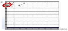
도 1a 및 도 1b는, 종래의 반도체 스토리지 시스템의 특정 블록 또는 특정 영역이 과도하게 사용된 예시적 그래프이다. 그래프의 X축은 어드레스를 나타내고, Y축은 삭제 횟수를 나타낸다.Figures 1A and 1B are exemplary graphs in which certain blocks or specific areas of conventional semiconductor storage systems are overused. The X-axis of the graph represents the address, and the Y-axis represents the number of times of deletion.
도 1a의 그래프를 참조하면, 어드레스 1500-2000번지 사이의 메모리 영역이 다른 메모리 영역보다 과도하게 사용된 용례를 나타낸다. 또한, 도 1b의 그래프를 참조하면, 다른 어드레스의 영역들은 아직 신선한(fresh) 메모리 상태를 가짐에도 불구하고, 특정 번지(편의상, a번지와 b번지)에서 과도하게 사용됨으로써 반도체 스토리지 시스템내 불량이 발생한 경우를 나타낸다.Referring to the graph of FIG. 1A, an example is shown in which a memory area between addresses 1500-2000 is used in excess of another memory area. Also, referring to the graph of FIG. 1B, it can be seen that although regions of different addresses still have a fresh memory state, they are overused at certain addresses (for convenience, addresses a and b) When it occurs.
공지된 바로는, 플래시 메모리를 구성하는 셀의 종류, 즉 SLC(Single Level Cell)의 경우에는 대략 100,000번 정도, MLC(Multi Level Cell)의 경우에는 대략 5000 ~10,000번 정도 삭제하면 그 수명이 다하는 것으로 알려져 있다. 따라서 SSD를 효율적으로 사용하기 위해서는 플래시 메모리의 모든 영역이 균등하게 사용되도록 관리하는 것이 매우 중요하게 되었다.It is known that the life of a flash memory is limited to about 100,000 times in the case of SLC (Single Level Cell) and about 5000 to 10,000 times in the case of MLC (Multi Level Cell) . Therefore, it is very important to manage all areas of flash memory to be used evenly in order to use SSD effectively.
이를 위해, 반도체 스토리지 시스템의 메인 컨트롤러(main controller)가 블록 단위로 웨어 레벨링(wear-leveling)을 수행하여 메모리 영역의 전체 블록의 사용 빈도를 적절히 관리하고 균등하게 사용하도록 제어하도록 하고 있다. 하지만, 이로 인해 메인 컨트롤러의 부하(load)는 더욱 증가하므로, 오히려 반도체 스토리 지 시스템 전체의 성능을 저하시킬 수 있는 요인이 되고 있다.To this end, the main controller of the semiconductor storage system carries out wear-leveling on a block-by-block basis to appropriately manage and evenly use the frequency of use of all blocks in the memory area. However, this causes the load of the main controller to increase, which may deteriorate the performance of the entire semiconductor storage system.
본 발명의 기술적 과제는 메모리 영역을 균등하게 사용하도록 제어하는 반도체 스토리지 시스템을 제공하는 것이다.SUMMARY OF THE INVENTION The present invention provides a semiconductor storage system that controls memory areas to be used evenly.
본 발명의 기술적 과제는 메모리 영역을 균등하게 사용하도록 제어하는 반도체 스토리지 시스템의 제어 방법을 제공하는 것이다.SUMMARY OF THE INVENTION It is an object of the present invention to provide a control method of a semiconductor storage system for controlling use of a memory area evenly.
본 발명의 기술적 과제를 달성하기 위하여, 일 실시예에 따른 본 발명의 반도체 스토리지 시스템은, 복수의 페이지를 포함하며, 상기 각 페이지에 대한 프로그램 관련 정보를 저장하는 메모리 영역 및 상기 프로그램 관련 정보에 따라 각 페이지의 프로그램 여부를 결정하는 메인 메모리 컨트롤러를 포함한다.According to an aspect of the present invention, there is provided a semiconductor storage system including a plurality of pages, a memory area for storing program related information for each page, And a main memory controller for determining whether to program each page.
본 발명의 기술적 과제를 달성하기 위하여, 다른 실시예에 따른 본 발명의 반도체 스토리지 시스템은, 복수의 칩을 포함하며 상기 각 칩은 복수의 페이지를 포함하며, 상기 페이지에 대한 프로그램 빈도를 저장하는 수명 관리부를 포함하는 메모리 영역 및 상기 메모리 영역으로부터 해당 페이지의 상기 프로그램 빈도를 수신하여 상기 해당 페이지의 프로그램 여부를 결정하는 메인 메모리 컨트롤러를 포함한다.According to another aspect of the present invention, there is provided a semiconductor storage system including a plurality of chips, each chip including a plurality of pages, And a main memory controller for receiving the program frequency of the page from the memory area and determining whether the corresponding page is programmed.
본 발명의 기술적 과제를 달성하기 위하여, 일 실시예에 따른 본 발명의 반도체 스토리지 시스템의 제어 방법은, 외부 프로그램 명령에 응답하여, 메모리 영역의 해당 페이지에 프로그램 펄스를 소정 전압 크기만큼 증가시키며 인가하는 단 계, 상기 프로그램 완료 시점의 상기 프로그램 펄스에 대한 횟수를 상기 메모리 영역내에 저장하는 단계 및 메인 메모리 컨트롤러가 상기 메모리 영역내 저장된 상기 프로그램 펄스 횟수를 이용하여 해당 페이지의 프로그램 여부를 결정하는 단계를 포함한다.According to an aspect of the present invention, there is provided a method of controlling a semiconductor storage system, the method comprising: increasing a program pulse to a corresponding page of a memory area in response to an external program command, Storing the number of times of the program pulse at the completion of the program in the memory area and determining whether the main memory controller is to program the page using the number of program pulses stored in the memory area do.
본 발명의 일 실시예에 따른 반도체 스토리지 시스템은 메인 메모리 컨트롤러의 부하를 감소시키면서도, 메모리 영역의 균등한 사용을 제어할 수 있다. 또한, 메인 메모리 컨트롤러의 작업 수행에 대한 부하가 감소됨으로써 반도체 스토리지 시스템의 속도 및 성능을 향상시킬 수 있다.The semiconductor storage system according to the embodiment of the present invention can control the uniform use of the memory area while reducing the load of the main memory controller. In addition, the speed and performance of the semiconductor storage system can be improved by reducing the load on the performance of the main memory controller.
이하에서는 본 발명의 일 실시예에 따른 반도체 스토리지 시스템에 대하여 첨부된 도면을 참조하여 설명하도록 한다.Hereinafter, a semiconductor storage system according to an embodiment of the present invention will be described with reference to the accompanying drawings.
도 2는 본 발명의 일 실시예에 따른 반도체 스토리지 시스템의 블록도이다.2 is a block diagram of a semiconductor storage system in accordance with one embodiment of the present invention.
도 2를 참조하면, 반도체 스토리지 시스템은 호스트 인터페이스(110), 메인 메모리 컨트롤러(120), MCU(Micro Control Unit) 및 메모리 영역(140)을 포함한다.Referring to FIG. 2, the semiconductor storage system includes a
우선, 호스트 인터페이스(110)는 메인 메모리 컨트롤러(120)와 연결되며, 외부 호스트 (미도시)와 메모리 컨트롤러(120)간에 제어 명령, 어드레스 신호 및 데이터 신호를 송수신한다. 호스트 인터페이스(110)와 외부 호스트 (미도시)간의 인터페이스 방식은 직렬 ATA(Serial Advanced Technology Attachment;SATA), 병렬 ATA(Parallel Advanced Technology attachment;PATA), SCSI, 익스프레스 카 드(Express Card) 및 피시아이-익스프레스(PCI-Express) 방식 중 어느 하나일 수 있으며 제한되지 않는다.The
메인 메모리 컨트롤러(120)는 메인 메모리 셀 어레이(140)의 복수개의 낸드 플래시 메모리 소자 중 소정 낸드 플래시 메모리 소자(미도시)를 선택하고, 프로그램, 삭제 또는 리드 명령을 제공한다. 또한, 본 발명의 일 실시예에 따르면, 메인 메모리 컨트롤러(120)는 메모리 영역(140)으로부터의 프로그램 펄스 횟수 정보를 이용하여 메모리 영역(140)의 균등한 사용을 제어할 수 있다. 이에 대한 상세한 설명은 후술하기로 한다.The
MCU(130)는 메인 메모리 컨트롤러(120)와 제어 명령, 어드레스 신호 및 데이터 신호등을 서로 송수신하거나, 정보등을 일부 저장한다. 이러한 MCU(130)내에는 통상 SRAM(Static Random Access Memory)과 같은 버퍼가 구비될 수 있다.The MCU 130 transmits / receives a control command, an address signal, and a data signal to / from the
메모리 영역(140)은 복수의 낸드 플래시 소자(미도시) 및 수명 관리부(148)를 포함한다. 메모리 영역(140)은 메인 메모리 컨트롤러(120)에 제어되어 복수의 낸드 플래시 소자를 통해 데이터의 프로그램, 삭제 및 리드 동작이 수행된다. 한편, 본 발명의 일 실시예에 따른 메모리 영역(140)은 수명 관리부(148)를 구비하여, 낸드 플래시 소자(미도시)의 프로그램 펄스 횟수를 저장할 수 있다.The
보다 구체적으로, 수명 관리부(148)는 데이터의 프로그램시 사용되는 프로그램 펄스의 횟수를 저장함으로써, 메모리 영역(140)에서 낸드 플래시 소자의 사용 빈도수를 간접적으로 체크할 수 있도록 한다. 즉, 메모리 영역(140)이 프로그램 펄스의 횟수를 메인 메모리 컨트롤러(120)에 제공하면, 메인 메모리 컨트롤러(120)는 프로그램 펄스의 횟수가 임계치인지 판단하여 임계치의 해당 페이지대신 다른 페이지에서 프로그램이 수행되도록 제어할 수 있다.More specifically, the
이와 같이, 본 발명의 일 실시예에 따르면 메모리 영역(140)이 낸드 플래시 소자내 페이지의 사용 빈도가 되는 프로그램 펄스 횟수를 저장하고, 메인 메모리 컨트롤러(120)에서 이러한 정보를 이용하도록 한다. 환언하면, 종래와 같이, 메인 메모리 컨트롤러(120)가 직접 메모리 영역(140)에 대해 웨어 레벨링을 수행하는 것은 많은 시간이 소요될 뿐 아니라, 웨어 레벨링 수행 시간동안 메인 메모리 컨트롤러(120)는 다른 작업을 처리하기 어려웠다. 하지만, 본 발명의 일 실시예에 따르면, 메인 메모리 컨트롤러(120)의 웨어 레벨링에 대한 작업 수행의 부담을 줄이면서도 균등한 메모리 영역(140)의 사용을 유도할 수 있다.As described above, according to an embodiment of the present invention, the
이에 대한 설명은 다음의 도면들을 참조하여 상세히 설명하기로 한다.The description will be made in detail with reference to the following drawings.
도 3은 수명 관리부(148)의 개념적인 블록도이다.FIG. 3 is a conceptual block diagram of the
수명 관리부(148)는 프로그램 제어부(142) 및 레지스터(146)를 포함한다.The
프로그램 제어부(142)는 외부 명령어에 응답하여 소정 전압의 프로그램 펄스(VPGM)를 낸드 플래시 소자(점선으로 표시)의 해당 페이지에 제공한다. 당업자라면 이미 잘 알고 있는 바와 같이, 낸드 플래시 소자의 프로그램은 페이지 단위로 수행되며, 해당 페이지의 워드라인에 고전압, 예컨대 18-20V의 전압을 인가하여 F-N 터널링 효과에 의해 전하가 플로팅 게이트에 축적되도록 하는 것이다.The
이때, 프로그램 전압 인가 방법은 증가형 스텝 펄스 프로그램(Incremental Step Pulse Programming; ISPP)방식을 이용하는 것으로 예시하나, 이에 제한되지 않는다. 우선, 프로그램 명령에 응답하여 소정 전압의 프로그램 펄스(VPGM)를 일단 인가하고 매 펄스 인가시마다 프로그램 성공 여부를 검증(verify)하면서 점차적으로 프로그램 펄스(VPGM)의 전압을 소정 전압만큼 증가시키는 방식이다. 따라서, 프로그램이 완성이 되기까지, 프로그램 제어부(142)는 소정 횟수 이상의 프로그램 펄스(VPGM)를 인가해야 하며, 프로그램이 성공하는 시점까지 프로그램 펄스 횟수(PCNT)를 계속 카운팅하도록 한다. 여기서의 프로그램 제어부(142)는 도시하지 않았으나 카운터를 포함하는 통상의 ISPP 방식의 프로그램 제어부로 예시하였다.At this time, the program voltage application method is exemplified by using the incremental step pulse programming (ISPP) method, but the present invention is not limited thereto. First, the way that one applies a program pulse (VPGM) of a predetermined voltage in response to a program instruction to increase by a predetermined voltage voltage gradually program pulse (VPGM) and verification (verify) for every program success applied every pulse to be. Therefore, until the program is completed, the
레지스터(146)는 프로그램이 성공된 시점의 카운팅된 프로그램 펄스 횟수(PCNT)를 저장한다.The
즉, 본 발명의 일 실시예에 따른 레지스터(146)는 페이지마다 프로그램 펄스 횟수(PCNT)를 저장하여, 메인 메모리 컨트롤러(120)에 제공하고, 이러한 과정을 반복하면서 페이지마다의 프로그램 펄스 횟수(PCNT)를 누적한다. 그리하여, 메인 메모리 컨트롤러(120)는 해당 페이지의 저장된 프로그램 펄스 횟수가 기 설정된 임계치인지 판단하여 임계치이면 해당 페이지의 수명 한계를 감지한다. 이에 따라, 메인 메모리 컨트롤러(120)는 해당 페이지에 추가의 프로그램이 수행되지 않도록 하고, 다음의 프로그램 명령에 응답하여 다른 페이지에서 수행되도록 제어할 수 있다.In other words, the
이로써, 본 발명의 일 실시예에 따르면, 수명 관리부(148)의 정보를 이용하 여 메모리 영역(140)의 수명 관리를 하는 것이 용이해질 수 있다. 한편, 설명의 편의상, 여기서는 낸드 플래시 소자가 블록당 128 페이지를 포함하는 것으로 예시한다.Thus, according to one embodiment of the present invention, it becomes easy to manage the life of the
다시 말하면, 특정 페이지가 빈번하게 프로그램된다면, 누적된 프로그램 펄스 횟수(PCNT)도 상당히 크고 상기 특정 페이지는 마모(wear-out)가 심할 것이다. 따라서, 이러한 경우, 상기 특정 페이지에는 추가의 프로그램이 수행되지 않도록 제어할 필요가 있다. 본 발명의 일 실시예에서는 메인 메모리 컨트롤러(120)가 레지스터(146)의 저장된 프로그램 펄스 횟수(PCNT)를 수신하여, 해당 페이지의 프로그램 여부만 제어함으로써, 메인 메모리 컨트롤러(120)의 작업 수행 부담이 경감될 수 있다.In other words, if a particular page is frequently programmed, the accumulated number of program pulses (PCNT) is also quite large and the particular page will wear-out too much. Therefore, in such a case, it is necessary to control so that an additional program is not performed on the specific page. The
도 4는 도 1에 따른 반도체 스토리지 시스템의 제어 방법을 나타낸 순서도이다.4 is a flowchart showing a control method of the semiconductor storage system according to FIG.
다시 도 1 내지 도 4를 참조하면, 외부로부터 프로그램 명령어가 입력된다(S10).1 to 4, a program command is inputted from the outside (S10).
그리하여, 프로그램 제어부(142)에서 우선 소정 전압을 갖는 프로그램 펄스를 인가한다(S20).Thus, the
프로그램 펄스(VPGM) 인가 후, 프로그램이 성공했는지 검증을 한다(S30).After the application of the program pulse VPGM , it is verified whether the program is successful (S30).
미처 프로그램되지 못했다면, 프로그램 펄스(VPGM)의 전압 크기를 기 설정된 전압 스텝(ΔV)만큼 증가시켜(S40), 이전 단계보다 높아진 전압을 갖는 프로그램 펄스를 다시 인가한다(S20).If the program has not been programmed yet, the voltage magnitude of the program pulse VPGM is increased by a predetermined voltage step? V in step S40, and the program pulse having a higher voltage than the previous step is applied again in step S20.
상기의 과정을 반복하여 프로그램이 성공했다면, 프로그램 펄스 스텝의 수를 카운팅하여 해당 페이지에 프로그램 펄스가 인가된 횟수를 레지스터(146)에 저장한 후, 메인 메모리 컨트롤러(120)에 제공한다(S50).If the program is successful, the number of program pulse steps is counted, and the number of times the program pulse is applied to the corresponding page is stored in the
메인 메모리 컨트롤러(120)는 프로그램 펄스 횟수가 임계치인지 판단한다(S60).The
그리하여, 해당 페이지의 프로그램 펄스 횟수가 임계치이면 불량 페이지 처리하여, 해당 페이지가 억세스되지 않도록 제어한다(S70).Thus, if the number of program pulses of the corresponding page is a threshold value, the defective page is processed so that the corresponding page is not accessed (S70).
하지만, 해당 페이지의 프로그램 펄스 횟수가 임계치를 초과하지 않으면 해당 페이지에서 계속 추가의 프로그램 명령이 수행되는 것을 허용한다(S80).However, if the number of program pulses of the page does not exceed the threshold value, the additional page instruction is allowed to be continuously executed in the page (S80).
이상과 같이, 본 발명의 일 실시예에 따른 반도체 스토리지 시스템은 페이지 단위로 프로그램 펄스 횟수를 카운팅하고, 이를 이용함으로써 전 메모리 영역(140)의 균등한 사용을 제어할 수 있다. 또한, 이러한 프로그램 펄스 횟수를 메모리 영역(140)내에 저장함으로써 메인 메모리 컨트롤러(120)의 작업 수행에 대한 부하를 경감시킬 수 있다. 더 나아가, 프로그램 펄스 횟수(PCNT)를 웨어 레벨링의 기준으로 이용함으로써, 블록 단위로 제어하는 종래의 수명 관리 방법보다 미세한 페이지 단위로 제어함으로써 메모리 영역(140)을 보다 효율적으로 관리할 수 있다. 이뿐 아니라, 웨어 레벨링의 기준이 되는 횟수에 대한 카운팅 및 저장의 작업이 메모리 영역(140)에 의해 수행하는 것이 가능해짐으로써, 메모리 영역(140)을 제어하는 다양한 컨트롤 유닛 또는 다양한 컨트롤러에 대해 보다 자유롭게 적용시킬 수 있다.As described above, the semiconductor storage system according to an embodiment of the present invention can control the uniform use of the
본 발명이 속하는 기술분야의 당업자는 본 발명이 그 기술적 사상이나 필수적 특징을 변경하지 않고서 다른 구체적인 형태로 실시될 수 있으므로, 이상에서 기술한 실시예들은 모든 면에서 예시적인 것이며 한정적인 것이 아닌 것으로서 이해해야만 한다. 본 발명의 범위는 상세한 설명보다는 후술하는 특허청구범위에 의하여 나타내어지며, 특허청구범위의 의미 및 범위 그리고 그 등가개념으로부터 도출되는 모든 변경 또는 변형된 형태가 본 발명의 범위에 포함되는 것으로 해석되어야 한다.It will be understood by those skilled in the art that various changes in form and details may be made therein without departing from the spirit and scope of the present invention as defined by the following claims and their equivalents. Only. It is intended that the present invention covers the modifications and variations of this invention provided they come within the scope of the appended claims and their equivalents. .
도 1a 및 도 1b는 종래의 불균등한 메모리 영역의 용례를 나타내는 그래프,FIGS. 1A and 1B are graphs illustrating examples of conventional unequal memory areas,
도 2는 본 발명의 일 실시예에 따른 반도체 스토리지 시스템의 블록도,2 is a block diagram of a semiconductor storage system in accordance with an embodiment of the present invention;
도 3은 도 2에 따른 수명 관리부의 개념적인 블록도, 및3 is a conceptual block diagram of the life management unit according to Fig. 2, and Fig.
도 4는 도 2에 따른 반도체 스토리지 시스템의 제어 방법을 나타낸 순서도이다.4 is a flowchart showing a control method of the semiconductor storage system according to FIG.
<도면의 주요 부분에 대한 부호의 설명>Description of the Related Art
110: 호스트 인터페이스 120: 메인 메모리 컨트롤러110: Host interface 120: Main memory controller
130: MCU 140: 메모리 영역130: MCU 140: memory area
142: 프로그램 제어부 146: 레지스터142: Program control section 146: Register
148: 수명 관리부148:
Claims (15)
Translated fromKoreanPriority Applications (4)
| Application Number | Priority Date | Filing Date | Title |
|---|---|---|---|
| KR1020090020225AKR101038991B1 (en) | 2009-03-10 | 2009-03-10 | Semiconductor storage system and its control method for even use of memory area |
| US12/493,861US8081517B2 (en) | 2009-03-10 | 2009-06-29 | Solid state storage system for uniformly using memory area and method controlling the same |
| TW098126207ATWI484332B (en) | 2009-03-10 | 2009-08-04 | Solid state storage system for uniformly using memory area and method controlling the same |
| US13/296,395US8902665B2 (en) | 2009-03-10 | 2011-11-15 | Solid state storage system for uniformly using memory area and method controlling the same |
Applications Claiming Priority (1)
| Application Number | Priority Date | Filing Date | Title |
|---|---|---|---|
| KR1020090020225AKR101038991B1 (en) | 2009-03-10 | 2009-03-10 | Semiconductor storage system and its control method for even use of memory area |
Publications (2)
| Publication Number | Publication Date |
|---|---|
| KR20100101825Atrue KR20100101825A (en) | 2010-09-20 |
| KR101038991B1 KR101038991B1 (en) | 2011-06-03 |
Family
ID=42730593
Family Applications (1)
| Application Number | Title | Priority Date | Filing Date |
|---|---|---|---|
| KR1020090020225AActiveKR101038991B1 (en) | 2009-03-10 | 2009-03-10 | Semiconductor storage system and its control method for even use of memory area |
Country Status (3)
| Country | Link |
|---|---|
| US (2) | US8081517B2 (en) |
| KR (1) | KR101038991B1 (en) |
| TW (1) | TWI484332B (en) |
Families Citing this family (7)
| Publication number | Priority date | Publication date | Assignee | Title |
|---|---|---|---|---|
| US8737130B2 (en)* | 2012-02-29 | 2014-05-27 | Sandisk Technologies Inc. | System and method of determining a programming step size for a word line of a memory |
| KR102258126B1 (en) | 2015-03-19 | 2021-05-28 | 삼성전자주식회사 | Method of operating a memory controller, a data storage device including same, and data processing system including same |
| KR20190005447A (en)* | 2017-07-06 | 2019-01-16 | 에스케이하이닉스 주식회사 | Memory system and method for operating semiconductor memory device |
| KR102524916B1 (en)* | 2018-03-13 | 2023-04-26 | 에스케이하이닉스 주식회사 | Storage device and operating method thereof |
| US10490288B1 (en)* | 2018-09-27 | 2019-11-26 | Seagate Technology Llc | Page-level reference voltage parameterization for solid statesolid state storage devices |
| US11010244B2 (en)* | 2019-09-16 | 2021-05-18 | Macronix International Co., Ltd. | Memory data management method |
| KR20210047198A (en)* | 2019-10-21 | 2021-04-29 | 에스케이하이닉스 주식회사 | Memory device |
Family Cites Families (16)
| Publication number | Priority date | Publication date | Assignee | Title |
|---|---|---|---|---|
| US20030163633A1 (en) | 2002-02-27 | 2003-08-28 | Aasheim Jered Donald | System and method for achieving uniform wear levels in a flash memory device |
| JP3833970B2 (en) | 2002-06-07 | 2006-10-18 | 株式会社東芝 | Nonvolatile semiconductor memory |
| US6985992B1 (en)* | 2002-10-28 | 2006-01-10 | Sandisk Corporation | Wear-leveling in non-volatile storage systems |
| EP1556868B1 (en)* | 2002-10-28 | 2007-09-05 | SanDisk Corporation | Automated wear leveling in non-volatile storage systems |
| US6944063B2 (en)* | 2003-01-28 | 2005-09-13 | Sandisk Corporation | Non-volatile semiconductor memory with large erase blocks storing cycle counts |
| US7818492B2 (en)* | 2004-02-26 | 2010-10-19 | Supertalent Electronics, Inc. | Source and shadow wear-leveling method and apparatus |
| US7441067B2 (en)* | 2004-11-15 | 2008-10-21 | Sandisk Corporation | Cyclic flash memory wear leveling |
| JP2007004892A (en)* | 2005-06-23 | 2007-01-11 | Toshiba Corp | Semiconductor integrated circuit device |
| US7236402B2 (en)* | 2005-11-30 | 2007-06-26 | Freescale Semiconductor, Inc. | Method and apparatus for programming/erasing a non-volatile memory |
| JP4901348B2 (en)* | 2006-07-20 | 2012-03-21 | 株式会社東芝 | Semiconductor memory device and control method thereof |
| KR101061932B1 (en)* | 2006-09-06 | 2011-09-02 | 후지쯔 가부시끼가이샤 | Nonvolatile memory |
| KR100857761B1 (en)* | 2007-06-14 | 2008-09-10 | 삼성전자주식회사 | Memory system performing wear leveling and its writing method |
| KR101413736B1 (en)* | 2007-09-13 | 2014-07-02 | 삼성전자주식회사 | Memory system with improved reliability and wear-leveling technique thereof |
| TWI373772B (en)* | 2007-10-04 | 2012-10-01 | Phison Electronics Corp | Wear leveling method and controller using the same |
| KR101401560B1 (en)* | 2007-12-13 | 2014-06-03 | 삼성전자주식회사 | Semiconductor memory system and wear-leveling method thereof |
| US8036035B2 (en)* | 2009-03-25 | 2011-10-11 | Micron Technology, Inc. | Erase cycle counter usage in a memory device |
- 2009
- 2009-03-10KRKR1020090020225Apatent/KR101038991B1/enactiveActive
- 2009-06-29USUS12/493,861patent/US8081517B2/enactiveActive
- 2009-08-04TWTW098126207Apatent/TWI484332B/enactive
- 2011
- 2011-11-15USUS13/296,395patent/US8902665B2/enactiveActive
Also Published As
| Publication number | Publication date |
|---|---|
| US20120124302A1 (en) | 2012-05-17 |
| TWI484332B (en) | 2015-05-11 |
| US20100232226A1 (en) | 2010-09-16 |
| TW201033806A (en) | 2010-09-16 |
| US8902665B2 (en) | 2014-12-02 |
| US8081517B2 (en) | 2011-12-20 |
| KR101038991B1 (en) | 2011-06-03 |
Similar Documents
| Publication | Publication Date | Title |
|---|---|---|
| US11860774B2 (en) | User device including a nonvolatile memory device and a data write method thereof | |
| US11226895B2 (en) | Controller and operation method thereof | |
| JP5222232B2 (en) | Scheduling housekeeping operations in flash memory systems | |
| US9298608B2 (en) | Biasing for wear leveling in storage systems | |
| KR102501751B1 (en) | Memory Controller, Non-volatile Memory System and Operating Method thereof | |
| JP6771621B1 (en) | Systems and methods to erase blocks with few programmed pages | |
| US8656256B2 (en) | Apparatus and method for multi-mode operation of a flash memory device | |
| US20180081589A1 (en) | Nonvolatile memory controller and method for erase suspend management that increments the number of program and erase cycles after erase suspend | |
| KR101038991B1 (en) | Semiconductor storage system and its control method for even use of memory area | |
| US9639463B1 (en) | Heuristic aware garbage collection scheme in storage systems | |
| JP2009503726A (en) | Context-sensitive memory performance | |
| US20170075610A1 (en) | Solid state memory system with power management mechanism and method of operation thereof | |
| US11537318B2 (en) | Memory system and operating method thereof | |
| US8549214B2 (en) | Protection against data corruption for multi-level memory cell (MLC) flash memory | |
| CN107924700B (en) | Adaptive multi-stage erase | |
| KR20080064476A (en) | How to store the erase count of flash memory devices | |
| US9466384B1 (en) | Memory device and associated erase method | |
| CN114724609B (en) | Memory device and method of operating the same | |
| KR101027687B1 (en) | Semiconductor storage system for controlling the light operation and its control method | |
| US9799407B2 (en) | Method for operating storage device managing wear level depending on reuse period | |
| KR100736093B1 (en) | NAD flash control device and method | |
| CN111949208A (en) | Virtual physical erasure of memory of a data storage device | |
| US20250284404A1 (en) | Memory system and control method thereof, and electronic apparatus |
Legal Events
| Date | Code | Title | Description |
|---|---|---|---|
| A201 | Request for examination | ||
| PA0109 | Patent application | Patent event code:PA01091R01D Comment text:Patent Application Patent event date:20090310 | |
| PA0201 | Request for examination | ||
| PG1501 | Laying open of application | ||
| E902 | Notification of reason for refusal | ||
| PE0902 | Notice of grounds for rejection | Comment text:Notification of reason for refusal Patent event date:20100929 Patent event code:PE09021S01D | |
| E701 | Decision to grant or registration of patent right | ||
| PE0701 | Decision of registration | Patent event code:PE07011S01D Comment text:Decision to Grant Registration Patent event date:20110427 | |
| GRNT | Written decision to grant | ||
| PR0701 | Registration of establishment | Comment text:Registration of Establishment Patent event date:20110530 Patent event code:PR07011E01D | |
| PR1002 | Payment of registration fee | Payment date:20110531 End annual number:3 Start annual number:1 | |
| PG1601 | Publication of registration | ||
| FPAY | Annual fee payment | Payment date:20140423 Year of fee payment:4 | |
| PR1001 | Payment of annual fee | Payment date:20140423 Start annual number:4 End annual number:4 | |
| FPAY | Annual fee payment | ||
| PR1001 | Payment of annual fee | ||
| FPAY | Annual fee payment | Payment date:20160422 Year of fee payment:6 | |
| PR1001 | Payment of annual fee | Payment date:20160422 Start annual number:6 End annual number:6 | |
| FPAY | Annual fee payment | Payment date:20170425 Year of fee payment:7 | |
| PR1001 | Payment of annual fee | Payment date:20170425 Start annual number:7 End annual number:7 | |
| FPAY | Annual fee payment | Payment date:20180425 Year of fee payment:8 | |
| PR1001 | Payment of annual fee | Payment date:20180425 Start annual number:8 End annual number:8 | |
| FPAY | Annual fee payment | Payment date:20190422 Year of fee payment:9 | |
| PR1001 | Payment of annual fee | Payment date:20190422 Start annual number:9 End annual number:9 | |
| PR1001 | Payment of annual fee | Payment date:20200424 Start annual number:10 End annual number:10 | |
| PR1001 | Payment of annual fee | Payment date:20220426 Start annual number:12 End annual number:12 | |
| PR1001 | Payment of annual fee | Payment date:20230425 Start annual number:13 End annual number:13 |