KR20100076274A - Phase changeable memory device and method of manufacturing the same - Google Patents
Phase changeable memory device and method of manufacturing the sameDownload PDFInfo
- Publication number
- KR20100076274A KR20100076274AKR1020080134269AKR20080134269AKR20100076274AKR 20100076274 AKR20100076274 AKR 20100076274AKR 1020080134269 AKR1020080134269 AKR 1020080134269AKR 20080134269 AKR20080134269 AKR 20080134269AKR 20100076274 AKR20100076274 AKR 20100076274A
- Authority
- KR
- South Korea
- Prior art keywords
- pattern
- phase change
- lower electrode
- electrode contact
- contact pattern
- Prior art date
- Legal status (The legal status is an assumption and is not a legal conclusion. Google has not performed a legal analysis and makes no representation as to the accuracy of the status listed.)
- Ceased
Links
Images


Classifications
- H—ELECTRICITY
- H10—SEMICONDUCTOR DEVICES; ELECTRIC SOLID-STATE DEVICES NOT OTHERWISE PROVIDED FOR
- H10N—ELECTRIC SOLID-STATE DEVICES NOT OTHERWISE PROVIDED FOR
- H10N70/00—Solid-state devices having no potential barriers, and specially adapted for rectifying, amplifying, oscillating or switching
- H10N70/20—Multistable switching devices, e.g. memristors
- H10N70/231—Multistable switching devices, e.g. memristors based on solid-state phase change, e.g. between amorphous and crystalline phases, Ovshinsky effect
- H—ELECTRICITY
- H10—SEMICONDUCTOR DEVICES; ELECTRIC SOLID-STATE DEVICES NOT OTHERWISE PROVIDED FOR
- H10B—ELECTRONIC MEMORY DEVICES
- H10B63/00—Resistance change memory devices, e.g. resistive RAM [ReRAM] devices
- H10B63/20—Resistance change memory devices, e.g. resistive RAM [ReRAM] devices comprising selection components having two electrodes, e.g. diodes
- H—ELECTRICITY
- H10—SEMICONDUCTOR DEVICES; ELECTRIC SOLID-STATE DEVICES NOT OTHERWISE PROVIDED FOR
- H10N—ELECTRIC SOLID-STATE DEVICES NOT OTHERWISE PROVIDED FOR
- H10N70/00—Solid-state devices having no potential barriers, and specially adapted for rectifying, amplifying, oscillating or switching
- H10N70/011—Manufacture or treatment of multistable switching devices
- H10N70/061—Shaping switching materials
- H10N70/068—Shaping switching materials by processes specially adapted for achieving sub-lithographic dimensions, e.g. using spacers
- H—ELECTRICITY
- H10—SEMICONDUCTOR DEVICES; ELECTRIC SOLID-STATE DEVICES NOT OTHERWISE PROVIDED FOR
- H10N—ELECTRIC SOLID-STATE DEVICES NOT OTHERWISE PROVIDED FOR
- H10N70/00—Solid-state devices having no potential barriers, and specially adapted for rectifying, amplifying, oscillating or switching
- H10N70/801—Constructional details of multistable switching devices
- H10N70/821—Device geometry
- H10N70/826—Device geometry adapted for essentially vertical current flow, e.g. sandwich or pillar type devices
- H10N70/8265—Device geometry adapted for essentially vertical current flow, e.g. sandwich or pillar type devices on sidewalls of dielectric structures, e.g. mesa-shaped or cup-shaped devices
- H—ELECTRICITY
- H10—SEMICONDUCTOR DEVICES; ELECTRIC SOLID-STATE DEVICES NOT OTHERWISE PROVIDED FOR
- H10N—ELECTRIC SOLID-STATE DEVICES NOT OTHERWISE PROVIDED FOR
- H10N70/00—Solid-state devices having no potential barriers, and specially adapted for rectifying, amplifying, oscillating or switching
- H10N70/801—Constructional details of multistable switching devices
- H10N70/881—Switching materials
- H10N70/882—Compounds of sulfur, selenium or tellurium, e.g. chalcogenides
- H10N70/8825—Selenides, e.g. GeSe
- H—ELECTRICITY
- H10—SEMICONDUCTOR DEVICES; ELECTRIC SOLID-STATE DEVICES NOT OTHERWISE PROVIDED FOR
- H10N—ELECTRIC SOLID-STATE DEVICES NOT OTHERWISE PROVIDED FOR
- H10N70/00—Solid-state devices having no potential barriers, and specially adapted for rectifying, amplifying, oscillating or switching
- H10N70/801—Constructional details of multistable switching devices
- H10N70/881—Switching materials
- H10N70/882—Compounds of sulfur, selenium or tellurium, e.g. chalcogenides
- H10N70/8828—Tellurides, e.g. GeSbTe
Landscapes
- Engineering & Computer Science (AREA)
- Manufacturing & Machinery (AREA)
- Semiconductor Memories (AREA)
Abstract
Translated fromKoreanDescription
Translated fromKorean본 발명은 상변화 메모리 소자 및 그 제조방법에 관한 것으로, 보다 구체적으로는 상변화막과 하부 전극 콘택간의 접촉 면적을 줄일 수 있는 상변화 메모리 소자 및 그 제조방법에 관한 것이다.The present invention relates to a phase change memory device and a method of manufacturing the same, and more particularly, to a phase change memory device and a method of manufacturing the same can reduce the contact area between the phase change film and the lower electrode contact.
IT 기술의 급격한 발전에 따라 대용량의 정보를 무선으로 처리하는 휴대 정보 통신 시스템 및 기기의 개발에 적합한 초고속 및 대용량등의 특성을 갖는 차세대 메모리 장치가 요구되고 있다. 차세대 반도체 메모리 장치는 일반적인 플래쉬 메모리 장치의 비휘발성, SRAM(Static Random Access Memory)의 고속 동작, 및 DRAM(Dynamic RAM)의 고집적성등을 포함하면서, 더 낮은 소비 전력이 요구된다. 이와 같은 차세대 반도체 메모리 장치로는 일반적인 메모리 장치에 비해 전력, 데이터의 유지 및 기입/독취 특성이 우수한 FRAM(Ferroelectric RAM), MRAM(Magnetic RAM), PRAM(Phase-change RAM) 또는 NFGM(Nano Floating Gate Memory)등의 소자가 연구되고 있다. 그 중 PRAM은 단순한 구조를 가지면서 저렴한 비용으로 제조될 수 있으며, 고속 동작이 가능하므로 차세대 반도체 메모리 장치로 활발히 연구되고 있 다.BACKGROUND With the rapid development of IT technology, there is a demand for a next generation memory device having characteristics such as ultra-high speed and large capacity suitable for the development of a portable information communication system and a device for processing a large amount of information wirelessly. Next-generation semiconductor memory devices require lower power consumption, including non-volatileness of general flash memory devices, high speed operation of static random access memory (SRAM), and high integration of dynamic RAM (DRAM). Such next-generation semiconductor memory devices include Ferroelectric RAM (FRAM), Magnetic RAM (MRAM), Phase-change RAM (PRAM), or Nano Floating Gate, which have better power, data retention, and write / read characteristics than conventional memory devices. Devices such as memory) have been studied. Among them, PRAM has a simple structure and can be manufactured at low cost, and is being actively researched as a next-generation semiconductor memory device because of its high speed operation.
PRAM은 인가되는 전류로부터 발생되는 열에 따라 그 결정 상태가 변화되는 상변화막을 갖는다. 현재 PRAM에 적용되는 상변화막으로는 게르마늄(Ge), 안티몬(Sb) 및 텔루트(Te)로 구성된 칼코게나이드 화합물(Ge-Sb-Te:GST)이 주로 이용되고 있다. GST와 같은 상변화막은 공급되는 전류의 크기 및 시간에 따라 발생되는 열에 의하여 그 결정 상태가 변화된다. 이와 같은 상변화막은 비정질 상태에서 높은 비저항을 갖고, 결정 상태에서는 낮은 비저항을 가지므로, 메모리 장치의 데이터 저장 매체로 사용될 수 있다.The PRAM has a phase change film whose crystal state changes in accordance with heat generated from an applied current. Currently, chalcogenide compounds (Ge-Sb-Te: GST) composed of germanium (Ge), antimony (Sb) and tellurium (Te) are mainly used as phase change films applied to PRAM. The phase change film such as GST changes its crystal state by heat generated according to the magnitude and time of the supplied current. Such a phase change film has a high resistivity in an amorphous state and a low resistivity in a crystalline state, and thus can be used as a data storage medium of a memory device.
이러한 상변화막은 그것의 하부에 위치된 하부 전극 콘택(Bottom electrode contact)으로 부터 열을 제공받아, 상변화가 이루어진다. 하부 전극 콘택은 하부의 스위칭 소자로부터 큰 온 전류를 제공받아, 상변화막에 가능한 한 많은 열을 제공하여야 한다. 이에 따라, 하부 전극 콘택은 비저항이 큰 물질로 이용되어야 하며, 상변화막과의 접촉 면적을 줄여야 한다.This phase change film receives heat from a bottom electrode contact located below it, and a phase change occurs. The lower electrode contact should receive a large on current from the lower switching element, providing as much heat as possible to the phase change film. Accordingly, the lower electrode contact should be used as a material having a high resistivity, and the contact area with the phase change film should be reduced.
그런데, 반도체 메모리 장치의 집적 밀도가 증대됨에 따라, 패턴 및 홀을 형성하기 위한 포토리소그라피 기술이 거의 한계에 봉착된 상태이므로, 원하는 리셋 전류를 얻기 위한 초미세 하부 전극 콘택을 형성하는 데 어려움이 있다.However, as the integration density of semiconductor memory devices increases, photolithography techniques for forming patterns and holes are almost at a limit, and thus, it is difficult to form ultra-fine lower electrode contacts for obtaining a desired reset current. .
따라서, 본 발명의 목적은 상변화막과 하부 전극 콘택간의 접촉 면적을 줄일 수 있는 상변화 메모리 소자 및 그 제조방법을 제공하는 것이다.Accordingly, it is an object of the present invention to provide a phase change memory device capable of reducing the contact area between a phase change film and a lower electrode contact and a method of manufacturing the same.
상기한 본 발명의 목적을 달성하기 위한 본 발명의 일실시예에 따른 상변화 메모리 소자는 하부 전극 콘택 패턴, 및 상기 하부 전극 콘택 패턴층의 측벽에 형성된 상변화 패턴을 포함하며, 상기 하부 전극 콘택 패턴의 두께에 따라 상기 하부 전극 콘택 패턴과 상기 상변화 패턴의 접촉 면적이 결정된다.A phase change memory device according to an embodiment of the present invention for achieving the object of the present invention includes a lower electrode contact pattern, and a phase change pattern formed on the sidewalls of the lower electrode contact pattern layer, the lower electrode contact The contact area between the lower electrode contact pattern and the phase change pattern is determined according to the thickness of the pattern.
또한, 본 발명의 다른 실시예에 따른 상변화 메모리 소자의 제조방법은 다음과 같다. 먼저, 스위칭 소자를 갖는 반도체 기판을 제공한 다음, 상기 반도체 기판 상부에 상기 스위칭 소자와 전기적으로 연결된 하부 전극 콘택 패턴을 형성한다. 그 후, 상기 하부 전극 콘택 패턴의 측벽과 콘택되도록 상변화 패턴을 형성한다. 이때, 상기 하부 전극 콘택 패턴의 두께에 따라 상기 하부 전극 콘택 패턴과 상기 상변화 패턴의 접촉 면적이 결정된다.In addition, a method of manufacturing a phase change memory device according to another embodiment of the present invention is as follows. First, a semiconductor substrate having a switching element is provided, and then a lower electrode contact pattern electrically connected to the switching element is formed on the semiconductor substrate. Thereafter, a phase change pattern is formed to contact the sidewall of the lower electrode contact pattern. In this case, a contact area between the lower electrode contact pattern and the phase change pattern is determined according to the thickness of the lower electrode contact pattern.
또한, 본 발명의 다른 실시예에 따른 상변화 메모리 소자는 PN 다이오드가 형성된 반도체 기판, 상기 PN 다이오드와 전기적으로 연결되며, 상기 PN 다이오드보다 넓은 선폭을 갖도록 형성된 하부 전극 콘택 패턴, 상기 하부 전극 콘택 패턴의 측벽에 형성된 상변화 패턴, 상기 상변화 패턴 사이의 공간에 매립된 층간 절연막, 및 상기 상변화 패턴 상부에 형성되며, 상기 상변화 패턴과 전기적으로 연결되 는 상부 전극을 포함하며, 상기 하부 전극 콘택 패턴의 두께에 따라 상기 하부 전극 콘택 패턴과 상기 상변화 패턴의 접촉 면적이 결정된다.In addition, a phase change memory device according to another exemplary embodiment of the present invention may include a semiconductor substrate on which a PN diode is formed, a lower electrode contact pattern and a lower electrode contact pattern that are electrically connected to the PN diode and have a wider line width than the PN diode. A phase change pattern formed on a sidewall of the substrate, an interlayer insulating layer buried in a space between the phase change patterns, and an upper electrode formed on the phase change pattern and electrically connected to the phase change pattern, wherein the lower electrode The contact area between the lower electrode contact pattern and the phase change pattern is determined according to the thickness of the contact pattern.
또한, 본 발명의 또 다른 실시예에 따른 상변화 메모리 소자의 제조방법은 다음과 같다. 먼저, 스위칭 소자를 갖는 반도체 기판을 준비한 다음, 상기 반도체 기판 상부에 상기 스위칭 소자와 전기적으로 연결된 하부 전극 콘택 패턴을 형성한다. 상기 하부 전극 콘택 패턴의 측벽과 콘택되도록 상변화 패턴을 형성한 후, 상기 상변화 패턴 사이의 공간에 평탄화된 층간 절연막을 매립한다. 다음, 상기 층간 절연막 상부에 상기 상변화 패턴과 전기적으로 연결되도록 상부 전극을 형성한다. 상기 하부 전극 콘택 패턴의 두께에 따라 상기 하부 전극 콘택 패턴과 상기 상변화 패턴의 접촉 면적이 결정된다.In addition, a method of manufacturing a phase change memory device according to still another embodiment of the present invention is as follows. First, a semiconductor substrate having a switching element is prepared, and then a lower electrode contact pattern electrically connected to the switching element is formed on the semiconductor substrate. After the phase change pattern is formed to contact the sidewall of the lower electrode contact pattern, the planarized interlayer insulating layer is buried in a space between the phase change patterns. Next, an upper electrode is formed on the interlayer insulating layer to be electrically connected to the phase change pattern. The contact area between the lower electrode contact pattern and the phase change pattern is determined according to the thickness of the lower electrode contact pattern.
본 발명에 따르면, 하부 전극 콘택층 측벽과 콘택되도록 상변화 패턴을 형성하므로써, 하부 전극 콘택 패턴과 상변화 패턴간의 콘택 면적을 하부 전극 콘택 패턴의 두께로 조절할 수 있다. 이에 따라, 하부 전극 콘택 패턴을 박막으로 형성하므로써, 하부 전극 콘택 패턴과 상변화 패턴간의 콘택 면적을 극소화할 수 있다.According to the present invention, the contact area between the lower electrode contact pattern and the phase change pattern may be adjusted to the thickness of the lower electrode contact pattern by forming the phase change pattern to contact the sidewalls of the lower electrode contact layer. Accordingly, by forming the lower electrode contact pattern in a thin film, the contact area between the lower electrode contact pattern and the phase change pattern can be minimized.
또한, 하부 전극 콘택 패턴을 스위칭 소자인 PN 다이오드보다 넓은 선폭을 갖도록 형성함에 따라, 충분한 콘택 면적을 확보하여 전기적 특성을 개선할 수 있다.In addition, since the lower electrode contact pattern is formed to have a wider line width than that of the PN diode as the switching element, a sufficient contact area may be secured to improve electrical characteristics.
이하, 첨부한 도면에 의거하여 본 발명의 바람직한 실시예를 설명하도록 한 다.Hereinafter, preferred embodiments of the present invention will be described with reference to the accompanying drawings.
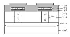
도 1을 참조하면, 반도체 기판(100)의 소정 부분에 n형의 불순물을 일반적인 모스 트랜지스터의 접합 영역 형태로 주입하여, 워드라인 영역(105)을 형성한다. 워드라인 영역(105)이 형성된 반도체 기판(100) 결과물 상부에 제 1 층간 절연막(110)을 형성한 후, 상기 워드라인 영역(105)의 소정 부분이 노출될 수 있도록 제 1 층간 절연막(110)을 식각하여, 콘택홀(도시되지 않음)을 형성한다. 상기 콘택홀내에 선택적 에피택셜 공정 및 불순물 이온 주입 공정을 통해 PN 다이오드(115)를 형성한다.Referring to FIG. 1, an n-type impurity is implanted into a predetermined portion of the
PN 다이오드(115)가 형성된 제 1 층간 절연막(110) 상부에 오믹 콘택층(120) 및 하부 전극 콘택층(122)을 순차적으로 증착한다. 이때, 하부 전극 콘택층(122)의 두께가 곧 이후 형성될 상변화막의 접촉 면적이 되므로, 접촉 면적 및 전류 전달 측면을 고려하여 하부 전극 콘택층(122)을 형성한다. 또한, 현재 반도체 제조 공정에서는 수 Å두께로도 막 증착이 가능하므로, 접촉 면적을 고려하여 하부 전극 콘택층(122)의 두께를 조절할 수 있다. 상기 오믹 콘택층(120)은 도전 특성이 우수한 코발트 실리사이드막(CoSi2)이 이용될 수 있으며, 여기에 한정되지 않고 다양한 실리사이드막이 이용될 수 있다. 또한, 하부 전극 콘택층(125)으로는 비저항이 큰 티타늄 질화막, 티타늄 알루미늄 질화막, 도핑된 폴리실리콘막 또는 도핑된 실리콘 저머늄막이 이용될 수 있다.The
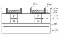
도 2를 참조하면, 상기 하부 전극 콘택층(122) 및 오믹 콘택층(120)을 상기 PN 다이오드(115) 상부에 각각 놓여지도록 패터닝한다. 도면 부호 125는 하부 전극 콘택 패턴을 지시한다. 여기서, 하부 전극 콘택 패턴(125) 및 오믹 콘택층(120)은 상기 PN 다이오드(115)의 직경(선폭) 보다 큰 선폭을 가질 수 있다. 이에 따라, PN 다이오드(115)와 하부 전극 콘택(125)간에 충분한 접촉 면적이 확보되어, 상변화 메모리 소자의 전류 특성을 개선할 수 있다. 다음, 상기 반도체 기판(100) 결과물 상부에 상변화막(130)을 증착한다.Referring to FIG. 2, the lower
도 3을 참조하면, 상변화막(130)이 상기 하부 전극 콘택층(125)의 양측에 위치할 수 있도록 상기 상변화막(130)의 소정 부분을 식각하여, 상변화 패턴(135a,135b)을 형성한다. 본 실시예에서의 상변화 패턴(135a,135b)은 하부 전극 콘택층(125) 양측에 각각 형성되어, 상변화 패턴(135a,135b)의 측벽에서 하부 전극 콘택층(125)과 콘택을 이루게 된다. 아울러, 상변화 패턴(135a,135b)과 하부 전극 콘택층(125)의 콘택 면적은 상기 하부 전극 콘택층(125)에 의해 조절 가능하므로, 미세한 콘택 면적을 확보할 수 있다. 이때, 상기 상변화 패턴(135a,135b)은 상기 하부 전극 콘택 패턴(125) 양측에 개별의 기둥 형태로 패터닝될 수도 있고, 또는 하부 전극 콘택 패턴(125)의 둘레를 따라 실린더 형태로 패터닝될 수 도 있다.Referring to FIG. 3, a predetermined portion of the
그 후, 상변화 패턴(135a,135b)이 형성된 반도체 기판(100) 결과물 상부에 제 2 층간 절연막(140)을 증착한 다음, 상기 제 2 층간 절연막(140) 및 상기 상변화 패턴(135a,135b)을 평탄화한다.Thereafter, the second
다음, 도 4를 참조하면, 상변화 패턴(135a,135b)과 각각 콘택되도록 상기 제 2 층간 절연막(140) 상부에 상부 전극(145a,145b)을 각각 형성한다. 이때, 상부 전극(145a,145b)은 상기 도 4와 같이, 상변화 패턴(135a,135b) 각각에 대해 개별적으로 형성될 수도 있고, 도 5에 도시된 것과 같이, 상기 상변화 패턴들(135a,135b)과 모두 콘택되도록 단일 형태로 상부 전극(145)을 형성할 수도 있다.Next, referring to FIG. 4,
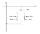
여기서, 상기 상변화 패턴(135a,135b)이 하나의 PN 다이오드(115)에 대해 각각 한 쌍씩 구비되는 경우를 등가 회로적으로 표시하면, 도 6에 도시된 바와 같이, 하나의 PN 다이오드(115)에 한 쌍의 상변화 패턴(135a,135b)이 병렬로 연결된 것으로 표현된다. 이와 같이 하나의 메모리 셀에, 복수의 상변화 패턴(135a,135b), 즉 복수의 저항이 연결됨에 따라, 멀티 비트를 실현할 수 있게 된다.Here, if the
도 7 내지 도 9는 본 발명의 다른 실시예에 따른 상변화 메모리 소자의 제조방법을 설명하기 위한 각 공정별 단면도들이다. 본 실시예는 상기 일 실시예에서 하부 전극 콘택층(122) 및 오믹 콘택층(120)을 형성하는 공정까지는 동일하며, 그 이후의 공정에 대해 자세히 설명할 것이다.7 to 9 are cross-sectional views of respective processes for describing a method of manufacturing a phase change memory device according to another exemplary embodiment of the present invention. The present embodiment is the same until the process of forming the lower
도 7을 참조하면, 상기 하부 전극 콘택층 상부에 희생 절연막을 소정 두께로 증착한다. 상기 희생 절연막은 이후 형성될 상변화 패턴의 높이(두께)를 한정하기 위한 막으로, 상변화 패턴의 높이를 고려하여 그 두께를 설정할 수 있다. 다음, 상기 희생 절연막, 하부 전극 콘택층 및 오믹 콘택층(120)을 상기 PN 다이오드(115) 상부에 위치될 수 있도록 소정 부분 패터닝하여, 하부 전극 콘택 패턴(125) 및 희생 패턴(127)을 형성한다. 그리고 나서, 상변화막을 상기 반도체 기판(100) 결과물 표면을 따라 소정 두께로 증착한다. 본 실시예에서 상변화막의 증착 두께는 이전 실시예의 상변화막의 증착 두께보다 작을 수 있다. 다음, 상기 상변화막을 비등방성 식각하여, 상기 희생 패턴(127), 하부 전극 콘택 패턴(125) 및 오믹 콘택층(120) 측벽에 스페이서 형태의 상변화 패턴(136)을 형성한다.Referring to FIG. 7, a sacrificial insulating film is deposited on the lower electrode contact layer to a predetermined thickness. The sacrificial insulating film is a film for defining the height (thickness) of the phase change pattern to be formed later, and may be set in consideration of the height of the phase change pattern. Next, the sacrificial insulating layer, the lower electrode contact layer, and the
다음, 도 8에 도시된 바와 같이, 상기 희생 패턴(127)을 선택적으로 제거한 다음, 반도체 기판(100) 결과물 상부에 제 2 층간 절연막(140)을 증착한다. 상기 제 2 층간 절연막(140)은 상기 상변화 패턴(136) 사이의 공간이 충분히 매립될 수 있을 정도의 두께로 증착한다.Next, as shown in FIG. 8, the
도 9를 참조하면, 상기 제 2 층간 절연막(140) 및 상기 상변화 패턴(136)을 화학적 기계적 연마하여, 반도체 기판(100) 결과물의 표면을 평탄하게 만든다. 여기서 미설명 도면 부호 140'은 평탄화된 제 2 층간 절연막을 나타내고, 136'은 평탄화된 상변화 패턴을 나타낸다. 다음, 평탄화된 반도체 기판(100) 결과물 상부에 상기 상변화 패턴(136')과 각각 콘택되도록 상부 전극(146')을 형성한다.Referring to FIG. 9, the surface of the
이렇게 형성된 상변화 패턴(136')은 도 10에 도시된 바와 같이, 상기 하부 전극 콘택 패턴(도시되지 않음)의 외곽을 따라 실린더 형태로 형성되고, 상부 전극(146') 역시 상기 상변화 패턴(136')과 콘택되도록 구성됨에 의해 상기 상변화 패턴(136')의 선폭보다는 큰 실린더 형태로 형성된다.As shown in FIG. 10, the
이와같은 본 실시예 역시, 하부 전극 콘택층(125)의 측벽과 상기 상변화 패턴(136')의 측벽에서 콘택이 이루어진다. 이에 따라, 하부 전극 콘택층(125)의 증착 두께 조절만으로, 상변화 패턴(136')과 하부 전극 콘택층(125)간의 접촉 면적을 효과적으로 줄일 수 있게 된다.In this embodiment, contact is also made on the sidewall of the lower
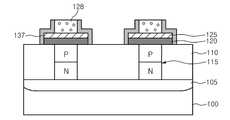
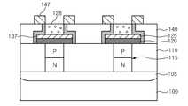
도 11 및 도 12는 본 발명의 또 다른 실시예에 따른 상변화 메모리 소자의 제조방법을 설명하기 위한 각 공정별 단면도이다. 본 실시예에서는 계단 형태의 상변화 패턴(137)을 제공할 것이다.11 and 12 are cross-sectional views of respective processes for explaining a method of manufacturing a phase change memory device according to still another embodiment of the present invention. In this embodiment, a
이와 같은 계단 형태의 상변화 패턴(137)을 제공하기 위해, 도 11에 도시된 것과 같이, PN 다이오드(115) 상에 오믹 콘택층(120)을 포함하는 하부 전극 콘택(125) 상에 상기 하부 전극 콘택 패턴(125)보다 좁은 선폭을 갖는 희생 패턴(128)을 형성한다. 이에 따라, 하부 전극 콘택 패턴(125)과 희생 패턴(128)의 측벽 부분에서, 상기 하부 전극 콘택층(125)과 희생 패턴(128) 사이에서 단차가 발생된다. 그 후, 오믹 콘택층(120), 하부 전극 콘택 패턴(125) 및 희생 패턴(128)의 표면을 따라 상변화막을 증착한 다음, 비등방성 식각을 이용하여 상변화막을 식각하므로써, 계단 형태의 상변화 패턴(137)을 형성한다. 상기 비등방성 식각은 예를 들어 방향성을 가지고 식각하는 방식으로서, 수평 또는 수직 방향에 위치하는 물질만을 선택적으로 제거하는 방식이다. 본 실시예에서는 반도체 기판(100)에 대해 평행한 면에 위치하는 상변화막을 선택적으로 제거하여 상변화 패턴(137)을 형성한다. 이때, 상기 비등방성 식각 공정시, 상기 하부 전극 콘택층(125) 상면에 위치하는 상변화막도 제거되어야 하나, 상기 희생 패턴(128)에 의해 노출되는 하부 전극 콘택층(125) 부분이 상대적으로 매우 협소하며 상기 희생 패턴(128)에 의해 식각 매체의 공급이 원할하지 않아, 하부 전극 콘택층(125) 상면에 상변화막이 잔류된다. 또한, 도 11에서 상변화 패턴(137)은 상면이 평탄하게 도시되어 있으나, 식각 정도에 따라, 상변화 패턴(137)의 상면은 첨점 형태로 구성될 수 있다.In order to provide the step-shaped
다음, 도 12에 도시된 바와 같이, 상변화 패턴(137) 사이의 공간이 충분히 매립될 수 있도록, 제 2 층간 절연막(140)을 증착한다. 이어서, 제 2 층간 절연막(140) 및 상변화 패턴(137)이 같은 높이가 될 수 있도록 평탄화, 즉, 화학적 기계적 연마 공정을 수행한다. 다음, 상기 상변화 패턴(137)과 콘택되도록 상기 제 2 층간 절연막(140) 상부에 상부 전극(147)을 형성한다.Next, as shown in FIG. 12, the second
이상에서 자세히 설명한 바와 같이, 본 발명에 따르면, 하부 전극 콘택층 측벽과 콘택되도록 상변화 패턴을 형성하므로써, 하부 전극 콘택층과 상변화 패턴간의 콘택 면적을 하부 전극 콘택층의 두께로 조절할 수 있다. 이에 따라, 하부 전극 콘택층을 박막으로 형성함으로써, 하부 전극 콘택층과 상변화 패턴간의 콘택 면적을 극소화할 수 있다.As described above in detail, according to the present invention, the contact area between the lower electrode contact layer and the phase change pattern may be adjusted to the thickness of the lower electrode contact layer by forming a phase change pattern to contact the sidewall of the lower electrode contact layer. Accordingly, by forming the lower electrode contact layer into a thin film, the contact area between the lower electrode contact layer and the phase change pattern can be minimized.
또한, 하부 전극 콘택층을 스위칭 소자인 PN 다이오드보다 넓은 선폭을 갖도록 형성함에 따라, 충분한 콘택 면적을 확보하여 전기적 특성을 개선할 수 있다.In addition, since the lower electrode contact layer is formed to have a wider line width than that of the PN diode as the switching element, a sufficient contact area may be secured to improve electrical characteristics.
본 발명은 상기한 실시예에 한정되는 것만은 아니다.The present invention is not limited to the above embodiment.
본 실시예에서는 오믹 콘택층을 하부 전극 콘택층과 같이 증착 후 패터닝하여 구성하였지만, PN 다이오드 상에 선택적 실리사이드 기법으로 형성할 수 있음은 물론이다.In the present exemplary embodiment, the ohmic contact layer is formed by depositing and patterning the same as the lower electrode contact layer. However, the ohmic contact layer may be formed on the PN diode by a selective silicide technique.
이상 본 발명을 바람직한 실시예를 들어 상세하게 설명하였으나, 본 발명은 상기 실시예에 한정되지 않고, 본 발명의 기술적 사상의 범위 내에서 당 분야에서 통상의 지식을 가진 자에 의하여 여러 가지 변형이 가능하다.Although the present invention has been described in detail with reference to preferred embodiments, the present invention is not limited to the above embodiments, and various modifications may be made by those skilled in the art within the scope of the technical idea of the present invention. Do.
도 1 내지 도 4는 본 발명의 일 실시예에 따른 상변화 메모리 소자의 제조방법을 설명하기 위한 각 공정별 단면도,1 to 4 are cross-sectional views for each process for explaining a method of manufacturing a phase change memory device according to an embodiment of the present invention;
도 5는 본 발명의 다른 실시예에 따른 상변화 메모리 소자의 단면도,5 is a cross-sectional view of a phase change memory device according to another embodiment of the present invention;
도 6은 본 발명의 일 실시예에 따른 상변화 메모리 소자의 등가 회로도,6 is an equivalent circuit diagram of a phase change memory device according to an embodiment of the present invention;
도 7 내지 도 9는 본 발명의 다른 실시예에 따른 상변화 메모리 소자의 제조방법을 설명하기 위한 각 공정별 단면도,7 to 9 are cross-sectional views of respective processes for explaining a method of manufacturing a phase change memory device according to another embodiment of the present invention;
도 10은 본 발명의 다른 실시예에 따른 상변화 메모리 소자의 상부 전극 및 상변화 패턴의 상면도, 및10 is a top view of an upper electrode and a phase change pattern of a phase change memory device according to another embodiment of the present invention; and
도 11 및 도 12는 본 발명의 또 다른 실시예에 따른 상변화 메모리 소자의 제조방법을 설명하기 위한 각 공정별 단면도이다.11 and 12 are cross-sectional views of respective processes for explaining a method of manufacturing a phase change memory device according to still another embodiment of the present invention.
<도면의 주요 부분에 대한 부호의 설명><Explanation of symbols for the main parts of the drawings>
100 : 반도체 기판 115 : PN 다이오드100
125 : 하부 전극 콘택 패턴 135a,135b,136,136',137 : 상변화 패턴125: lower
Claims (33)
Translated fromKoreanPriority Applications (2)
| Application Number | Priority Date | Filing Date | Title |
|---|---|---|---|
| KR1020080134269AKR20100076274A (en) | 2008-12-26 | 2008-12-26 | Phase changeable memory device and method of manufacturing the same |
| US12/493,562US20100163820A1 (en) | 2008-12-26 | 2009-06-29 | Phase change memory device having a reduced contact area and method for manufacturing the same |
Applications Claiming Priority (1)
| Application Number | Priority Date | Filing Date | Title |
|---|---|---|---|
| KR1020080134269AKR20100076274A (en) | 2008-12-26 | 2008-12-26 | Phase changeable memory device and method of manufacturing the same |
Publications (1)
| Publication Number | Publication Date |
|---|---|
| KR20100076274Atrue KR20100076274A (en) | 2010-07-06 |
Family
ID=42283712
Family Applications (1)
| Application Number | Title | Priority Date | Filing Date |
|---|---|---|---|
| KR1020080134269ACeasedKR20100076274A (en) | 2008-12-26 | 2008-12-26 | Phase changeable memory device and method of manufacturing the same |
Country Status (2)
| Country | Link |
|---|---|
| US (1) | US20100163820A1 (en) |
| KR (1) | KR20100076274A (en) |
Families Citing this family (24)
| Publication number | Priority date | Publication date | Assignee | Title |
|---|---|---|---|---|
| US7768812B2 (en) | 2008-01-15 | 2010-08-03 | Micron Technology, Inc. | Memory cells, memory cell programming methods, memory cell reading methods, memory cell operating methods, and memory devices |
| US8034655B2 (en) | 2008-04-08 | 2011-10-11 | Micron Technology, Inc. | Non-volatile resistive oxide memory cells, non-volatile resistive oxide memory arrays, and methods of forming non-volatile resistive oxide memory cells and memory arrays |
| US8211743B2 (en)* | 2008-05-02 | 2012-07-03 | Micron Technology, Inc. | Methods of forming non-volatile memory cells having multi-resistive state material between conductive electrodes |
| US8134137B2 (en)* | 2008-06-18 | 2012-03-13 | Micron Technology, Inc. | Memory device constructions, memory cell forming methods, and semiconductor construction forming methods |
| US9343665B2 (en) | 2008-07-02 | 2016-05-17 | Micron Technology, Inc. | Methods of forming a non-volatile resistive oxide memory cell and methods of forming a non-volatile resistive oxide memory array |
| US8411477B2 (en) | 2010-04-22 | 2013-04-02 | Micron Technology, Inc. | Arrays of vertically stacked tiers of non-volatile cross point memory cells, methods of forming arrays of vertically stacked tiers of non-volatile cross point memory cells, and methods of reading a data value stored by an array of vertically stacked tiers of non-volatile cross point memory cells |
| US8427859B2 (en) | 2010-04-22 | 2013-04-23 | Micron Technology, Inc. | Arrays of vertically stacked tiers of non-volatile cross point memory cells, methods of forming arrays of vertically stacked tiers of non-volatile cross point memory cells, and methods of reading a data value stored by an array of vertically stacked tiers of non-volatile cross point memory cells |
| US8289763B2 (en) | 2010-06-07 | 2012-10-16 | Micron Technology, Inc. | Memory arrays |
| US8351242B2 (en) | 2010-09-29 | 2013-01-08 | Micron Technology, Inc. | Electronic devices, memory devices and memory arrays |
| US8759809B2 (en) | 2010-10-21 | 2014-06-24 | Micron Technology, Inc. | Integrated circuitry comprising nonvolatile memory cells having platelike electrode and ion conductive material layer |
| US8796661B2 (en) | 2010-11-01 | 2014-08-05 | Micron Technology, Inc. | Nonvolatile memory cells and methods of forming nonvolatile memory cell |
| US8526213B2 (en) | 2010-11-01 | 2013-09-03 | Micron Technology, Inc. | Memory cells, methods of programming memory cells, and methods of forming memory cells |
| US9454997B2 (en) | 2010-12-02 | 2016-09-27 | Micron Technology, Inc. | Array of nonvolatile memory cells having at least five memory cells per unit cell, having a plurality of the unit cells which individually comprise three elevational regions of programmable material, and/or having a continuous volume having a combination of a plurality of vertically oriented memory cells and a plurality of horizontally oriented memory cells; array of vertically stacked tiers of nonvolatile memory cells |
| CN102569645A (en)* | 2010-12-17 | 2012-07-11 | 中芯国际集成电路制造(上海)有限公司 | PCM (phase change memory) and forming method thereof |
| US8431458B2 (en) | 2010-12-27 | 2013-04-30 | Micron Technology, Inc. | Methods of forming a nonvolatile memory cell and methods of forming an array of nonvolatile memory cells |
| US8791447B2 (en) | 2011-01-20 | 2014-07-29 | Micron Technology, Inc. | Arrays of nonvolatile memory cells and methods of forming arrays of nonvolatile memory cells |
| US8488365B2 (en) | 2011-02-24 | 2013-07-16 | Micron Technology, Inc. | Memory cells |
| US8537592B2 (en) | 2011-04-15 | 2013-09-17 | Micron Technology, Inc. | Arrays of nonvolatile memory cells and methods of forming arrays of nonvolatile memory cells |
| CN105098072B (en)* | 2015-07-30 | 2017-08-08 | 江苏时代全芯存储科技有限公司 | The manufacture method of phase-change memory |
| CN105226181A (en)* | 2015-09-01 | 2016-01-06 | 宁波时代全芯科技有限公司 | Phase-change memory and manufacture method thereof |
| CN105428525B (en)* | 2015-11-06 | 2018-03-02 | 江苏时代全芯存储科技有限公司 | Phase change memory and manufacturing method thereof |
| CN108172684B (en)* | 2015-12-16 | 2021-01-05 | 江苏时代全芯存储科技股份有限公司 | Phase change memory and manufacturing method thereof |
| CN105428533B (en)* | 2015-12-24 | 2018-05-15 | 江苏时代全芯存储科技有限公司 | Manufacturing method of phase change memory |
| US9685484B1 (en)* | 2016-07-20 | 2017-06-20 | Sandisk Technologies Llc | Reversible resistivity memory with crystalline silicon bit line |
Family Cites Families (18)
| Publication number | Priority date | Publication date | Assignee | Title |
|---|---|---|---|---|
| WO2001071807A1 (en)* | 2000-03-24 | 2001-09-27 | Fujitsu Limited | Semiconductor device and method of manufacture thereof |
| US6864503B2 (en)* | 2002-08-09 | 2005-03-08 | Macronix International Co., Ltd. | Spacer chalcogenide memory method and device |
| KR100448908B1 (en)* | 2002-09-03 | 2004-09-16 | 삼성전자주식회사 | Phase-changeable memory device structure and method for fabricating the same |
| TWI252539B (en)* | 2004-03-12 | 2006-04-01 | Toshiba Corp | Semiconductor device and manufacturing method therefor |
| US7381619B2 (en)* | 2004-04-27 | 2008-06-03 | Taiwan Semiconductor Manufacturing Company, Ltd. | Dual work-function metal gates |
| US7608503B2 (en)* | 2004-11-22 | 2009-10-27 | Macronix International Co., Ltd. | Side wall active pin memory and manufacturing method |
| US7504652B2 (en)* | 2005-07-13 | 2009-03-17 | Taiwan Semiconductor Manufacturing Company, Ltd. | Phase change random access memory |
| US7812334B2 (en)* | 2006-04-04 | 2010-10-12 | Micron Technology, Inc. | Phase change memory elements using self-aligned phase change material layers and methods of making and using same |
| US7560723B2 (en)* | 2006-08-29 | 2009-07-14 | Micron Technology, Inc. | Enhanced memory density resistance variable memory cells, arrays, devices and systems including the same, and methods of fabrication |
| US7863655B2 (en)* | 2006-10-24 | 2011-01-04 | Macronix International Co., Ltd. | Phase change memory cells with dual access devices |
| TWI327374B (en)* | 2007-01-10 | 2010-07-11 | Promos Technologies Inc | Phase change memory device and method of fabricating the same |
| TWI345827B (en)* | 2007-01-10 | 2011-07-21 | Nanya Technology Corp | Phase change memory device and method of fabricating the same |
| KR100881055B1 (en)* | 2007-06-20 | 2009-01-30 | 삼성전자주식회사 | Phase change memory unit, manufacturing method thereof, phase change memory device including same and manufacturing method thereof |
| KR100979235B1 (en)* | 2007-11-07 | 2010-08-31 | 주식회사 하이닉스반도체 | Phase change memory device and manufacturing method thereof |
| TWI426604B (en)* | 2008-06-03 | 2014-02-11 | Higgs Opl Capital Llc | Phase-change memory devices and methods for fabricating the same |
| US7919768B2 (en)* | 2008-07-11 | 2011-04-05 | Industrial Technology Research Institute | Phase-change memory element |
| KR101013445B1 (en)* | 2008-09-19 | 2011-02-14 | 주식회사 하이닉스반도체 | Phase change memory device having a heating electrode having minute contact area and manufacturing method thereof |
| US8604457B2 (en)* | 2008-11-12 | 2013-12-10 | Higgs Opl. Capital Llc | Phase-change memory element |
- 2008
- 2008-12-26KRKR1020080134269Apatent/KR20100076274A/ennot_activeCeased
- 2009
- 2009-06-29USUS12/493,562patent/US20100163820A1/ennot_activeAbandoned
Also Published As
| Publication number | Publication date |
|---|---|
| US20100163820A1 (en) | 2010-07-01 |
Similar Documents
| Publication | Publication Date | Title |
|---|---|---|
| KR20100076274A (en) | Phase changeable memory device and method of manufacturing the same | |
| US10381411B2 (en) | Three-dimensional memory device containing conformal wrap around phase change material and method of manufacturing the same | |
| KR101069724B1 (en) | Phase Change Memory Having 3 Dimension Stack Structure and Method of Manufacturing the Same | |
| US8921180B2 (en) | High-integration semiconductor memory device and method of manufacturing the same | |
| US20180114813A1 (en) | Double patterning method to form sub-lithographic pillars | |
| US9196827B2 (en) | Non-volatile memory devices having dual heater configurations and methods of fabricating the same | |
| US7723716B2 (en) | Phase change memory device | |
| WO2019023071A1 (en) | Self-aligned memory decks in cross-point memory arrays | |
| US9118010B2 (en) | Variable resistance memory device and method of fabricating the same | |
| JP2009212369A (en) | Semiconductor device, manufacturing method of semiconductor device and data processing system | |
| US20110266516A1 (en) | Phase change memory device capable of reducing disturbance and method of manufacturing the same | |
| CN101944568A (en) | Phase change memory cell with self-aligned vertical heater and low resistivity interface | |
| KR100935591B1 (en) | Phase change memory device capable of improving contact resistance and reset current and manufacturing method thereof | |
| KR100869843B1 (en) | Manufacturing method of phase change memory device | |
| KR101071191B1 (en) | Phase change memory device and manufacturing method thereof | |
| US8536013B2 (en) | Forming phase change memory cells | |
| KR101298258B1 (en) | Method of manufacturing phase-change memory device | |
| US20160104746A1 (en) | Methods of fabricating a variable resistance memory device using masking and selective removal | |
| KR101038997B1 (en) | Phase change memory device capable of reducing disturbance and method of manufacturing the same | |
| KR101119222B1 (en) | a Method of manufacturing Phase Change RAM having controllable contact area of bottom electrode contact | |
| KR102457047B1 (en) | Dimensional control of ridge lines | |
| KR20120016839A (en) | Manufacturing Method of Phase Change Memory Device | |
| KR101046228B1 (en) | Phase change memory device and manufacturing method thereof | |
| KR101094983B1 (en) | Manufacturing Method of Phase Change Device | |
| KR100831159B1 (en) | Phase change memory and its manufacturing method |
Legal Events
| Date | Code | Title | Description |
|---|---|---|---|
| A201 | Request for examination | ||
| PA0109 | Patent application | Patent event code:PA01091R01D Comment text:Patent Application Patent event date:20081226 | |
| PA0201 | Request for examination | ||
| PG1501 | Laying open of application | ||
| E902 | Notification of reason for refusal | ||
| PE0902 | Notice of grounds for rejection | Comment text:Notification of reason for refusal Patent event date:20101020 Patent event code:PE09021S01D | |
| E601 | Decision to refuse application | ||
| PE0601 | Decision on rejection of patent | Patent event date:20101227 Comment text:Decision to Refuse Application Patent event code:PE06012S01D Patent event date:20101020 Comment text:Notification of reason for refusal Patent event code:PE06011S01I |