KR20100050750A - Wafer level chip on chip package, package on package improving solder joint reliability but reducing mounting height and manufacturing method thereof - Google Patents
Wafer level chip on chip package, package on package improving solder joint reliability but reducing mounting height and manufacturing method thereofDownload PDFInfo
- Publication number
- KR20100050750A KR20100050750AKR1020080109802AKR20080109802AKR20100050750AKR 20100050750 AKR20100050750 AKR 20100050750AKR 1020080109802 AKR1020080109802 AKR 1020080109802AKR 20080109802 AKR20080109802 AKR 20080109802AKR 20100050750 AKR20100050750 AKR 20100050750A
- Authority
- KR
- South Korea
- Prior art keywords
- package
- chip
- semiconductor chip
- substrate
- silicon wafer
- Prior art date
- Legal status (The legal status is an assumption and is not a legal conclusion. Google has not performed a legal analysis and makes no representation as to the accuracy of the status listed.)
- Granted
Links
Images


Classifications
- H—ELECTRICITY
- H01—ELECTRIC ELEMENTS
- H01L—SEMICONDUCTOR DEVICES NOT COVERED BY CLASS H10
- H01L23/00—Details of semiconductor or other solid state devices
- H01L23/12—Mountings, e.g. non-detachable insulating substrates
- H—ELECTRICITY
- H01—ELECTRIC ELEMENTS
- H01L—SEMICONDUCTOR DEVICES NOT COVERED BY CLASS H10
- H01L25/00—Assemblies consisting of a plurality of semiconductor or other solid state devices
- H01L25/18—Assemblies consisting of a plurality of semiconductor or other solid state devices the devices being of the types provided for in two or more different main groups of the same subclass of H10B, H10D, H10F, H10H, H10K or H10N
- H—ELECTRICITY
- H01—ELECTRIC ELEMENTS
- H01L—SEMICONDUCTOR DEVICES NOT COVERED BY CLASS H10
- H01L23/00—Details of semiconductor or other solid state devices
- H01L23/48—Arrangements for conducting electric current to or from the solid state body in operation, e.g. leads, terminal arrangements ; Selection of materials therefor
- H—ELECTRICITY
- H01—ELECTRIC ELEMENTS
- H01L—SEMICONDUCTOR DEVICES NOT COVERED BY CLASS H10
- H01L24/00—Arrangements for connecting or disconnecting semiconductor or solid-state bodies; Methods or apparatus related thereto
- H01L24/93—Batch processes
- H01L24/95—Batch processes at chip-level, i.e. with connecting carried out on a plurality of singulated devices, i.e. on diced chips
- H01L24/97—Batch processes at chip-level, i.e. with connecting carried out on a plurality of singulated devices, i.e. on diced chips the devices being connected to a common substrate, e.g. interposer, said common substrate being separable into individual assemblies after connecting
- H—ELECTRICITY
- H01—ELECTRIC ELEMENTS
- H01L—SEMICONDUCTOR DEVICES NOT COVERED BY CLASS H10
- H01L25/00—Assemblies consisting of a plurality of semiconductor or other solid state devices
- H01L25/03—Assemblies consisting of a plurality of semiconductor or other solid state devices all the devices being of a type provided for in a single subclass of subclasses H10B, H10D, H10F, H10H, H10K or H10N, e.g. assemblies of rectifier diodes
- H01L25/04—Assemblies consisting of a plurality of semiconductor or other solid state devices all the devices being of a type provided for in a single subclass of subclasses H10B, H10D, H10F, H10H, H10K or H10N, e.g. assemblies of rectifier diodes the devices not having separate containers
- H01L25/065—Assemblies consisting of a plurality of semiconductor or other solid state devices all the devices being of a type provided for in a single subclass of subclasses H10B, H10D, H10F, H10H, H10K or H10N, e.g. assemblies of rectifier diodes the devices not having separate containers the devices being of a type provided for in group H10D89/00
- H01L25/0657—Stacked arrangements of devices
- H—ELECTRICITY
- H01—ELECTRIC ELEMENTS
- H01L—SEMICONDUCTOR DEVICES NOT COVERED BY CLASS H10
- H01L25/00—Assemblies consisting of a plurality of semiconductor or other solid state devices
- H01L25/03—Assemblies consisting of a plurality of semiconductor or other solid state devices all the devices being of a type provided for in a single subclass of subclasses H10B, H10D, H10F, H10H, H10K or H10N, e.g. assemblies of rectifier diodes
- H01L25/10—Assemblies consisting of a plurality of semiconductor or other solid state devices all the devices being of a type provided for in a single subclass of subclasses H10B, H10D, H10F, H10H, H10K or H10N, e.g. assemblies of rectifier diodes the devices having separate containers
- H01L25/105—Assemblies consisting of a plurality of semiconductor or other solid state devices all the devices being of a type provided for in a single subclass of subclasses H10B, H10D, H10F, H10H, H10K or H10N, e.g. assemblies of rectifier diodes the devices having separate containers the devices being integrated devices of class H10
- H—ELECTRICITY
- H01—ELECTRIC ELEMENTS
- H01L—SEMICONDUCTOR DEVICES NOT COVERED BY CLASS H10
- H01L25/00—Assemblies consisting of a plurality of semiconductor or other solid state devices
- H01L25/50—Multistep manufacturing processes of assemblies consisting of devices, the devices being individual devices of subclass H10D or integrated devices of class H10
- H—ELECTRICITY
- H01—ELECTRIC ELEMENTS
- H01L—SEMICONDUCTOR DEVICES NOT COVERED BY CLASS H10
- H01L2224/00—Indexing scheme for arrangements for connecting or disconnecting semiconductor or solid-state bodies and methods related thereto as covered by H01L24/00
- H01L2224/01—Means for bonding being attached to, or being formed on, the surface to be connected, e.g. chip-to-package, die-attach, "first-level" interconnects; Manufacturing methods related thereto
- H01L2224/26—Layer connectors, e.g. plate connectors, solder or adhesive layers; Manufacturing methods related thereto
- H01L2224/31—Structure, shape, material or disposition of the layer connectors after the connecting process
- H01L2224/32—Structure, shape, material or disposition of the layer connectors after the connecting process of an individual layer connector
- H01L2224/321—Disposition
- H01L2224/32151—Disposition the layer connector connecting between a semiconductor or solid-state body and an item not being a semiconductor or solid-state body, e.g. chip-to-substrate, chip-to-passive
- H01L2224/32221—Disposition the layer connector connecting between a semiconductor or solid-state body and an item not being a semiconductor or solid-state body, e.g. chip-to-substrate, chip-to-passive the body and the item being stacked
- H01L2224/32225—Disposition the layer connector connecting between a semiconductor or solid-state body and an item not being a semiconductor or solid-state body, e.g. chip-to-substrate, chip-to-passive the body and the item being stacked the item being non-metallic, e.g. insulating substrate with or without metallisation
- H—ELECTRICITY
- H01—ELECTRIC ELEMENTS
- H01L—SEMICONDUCTOR DEVICES NOT COVERED BY CLASS H10
- H01L2224/00—Indexing scheme for arrangements for connecting or disconnecting semiconductor or solid-state bodies and methods related thereto as covered by H01L24/00
- H01L2224/01—Means for bonding being attached to, or being formed on, the surface to be connected, e.g. chip-to-package, die-attach, "first-level" interconnects; Manufacturing methods related thereto
- H01L2224/42—Wire connectors; Manufacturing methods related thereto
- H01L2224/44—Structure, shape, material or disposition of the wire connectors prior to the connecting process
- H01L2224/45—Structure, shape, material or disposition of the wire connectors prior to the connecting process of an individual wire connector
- H01L2224/45001—Core members of the connector
- H01L2224/45099—Material
- H01L2224/451—Material with a principal constituent of the material being a metal or a metalloid, e.g. boron (B), silicon (Si), germanium (Ge), arsenic (As), antimony (Sb), tellurium (Te) and polonium (Po), and alloys thereof
- H01L2224/45138—Material with a principal constituent of the material being a metal or a metalloid, e.g. boron (B), silicon (Si), germanium (Ge), arsenic (As), antimony (Sb), tellurium (Te) and polonium (Po), and alloys thereof the principal constituent melting at a temperature of greater than or equal to 950°C and less than 1550°C
- H01L2224/45139—Silver (Ag) as principal constituent
- H—ELECTRICITY
- H01—ELECTRIC ELEMENTS
- H01L—SEMICONDUCTOR DEVICES NOT COVERED BY CLASS H10
- H01L2224/00—Indexing scheme for arrangements for connecting or disconnecting semiconductor or solid-state bodies and methods related thereto as covered by H01L24/00
- H01L2224/01—Means for bonding being attached to, or being formed on, the surface to be connected, e.g. chip-to-package, die-attach, "first-level" interconnects; Manufacturing methods related thereto
- H01L2224/42—Wire connectors; Manufacturing methods related thereto
- H01L2224/47—Structure, shape, material or disposition of the wire connectors after the connecting process
- H01L2224/48—Structure, shape, material or disposition of the wire connectors after the connecting process of an individual wire connector
- H01L2224/4805—Shape
- H01L2224/4809—Loop shape
- H01L2224/48091—Arched
- H—ELECTRICITY
- H01—ELECTRIC ELEMENTS
- H01L—SEMICONDUCTOR DEVICES NOT COVERED BY CLASS H10
- H01L2224/00—Indexing scheme for arrangements for connecting or disconnecting semiconductor or solid-state bodies and methods related thereto as covered by H01L24/00
- H01L2224/01—Means for bonding being attached to, or being formed on, the surface to be connected, e.g. chip-to-package, die-attach, "first-level" interconnects; Manufacturing methods related thereto
- H01L2224/42—Wire connectors; Manufacturing methods related thereto
- H01L2224/47—Structure, shape, material or disposition of the wire connectors after the connecting process
- H01L2224/48—Structure, shape, material or disposition of the wire connectors after the connecting process of an individual wire connector
- H01L2224/481—Disposition
- H01L2224/48135—Connecting between different semiconductor or solid-state bodies, i.e. chip-to-chip
- H01L2224/48145—Connecting between different semiconductor or solid-state bodies, i.e. chip-to-chip the bodies being stacked
- H—ELECTRICITY
- H01—ELECTRIC ELEMENTS
- H01L—SEMICONDUCTOR DEVICES NOT COVERED BY CLASS H10
- H01L2224/00—Indexing scheme for arrangements for connecting or disconnecting semiconductor or solid-state bodies and methods related thereto as covered by H01L24/00
- H01L2224/01—Means for bonding being attached to, or being formed on, the surface to be connected, e.g. chip-to-package, die-attach, "first-level" interconnects; Manufacturing methods related thereto
- H01L2224/42—Wire connectors; Manufacturing methods related thereto
- H01L2224/47—Structure, shape, material or disposition of the wire connectors after the connecting process
- H01L2224/48—Structure, shape, material or disposition of the wire connectors after the connecting process of an individual wire connector
- H01L2224/481—Disposition
- H01L2224/48151—Connecting between a semiconductor or solid-state body and an item not being a semiconductor or solid-state body, e.g. chip-to-substrate, chip-to-passive
- H01L2224/48221—Connecting between a semiconductor or solid-state body and an item not being a semiconductor or solid-state body, e.g. chip-to-substrate, chip-to-passive the body and the item being stacked
- H01L2224/48225—Connecting between a semiconductor or solid-state body and an item not being a semiconductor or solid-state body, e.g. chip-to-substrate, chip-to-passive the body and the item being stacked the item being non-metallic, e.g. insulating substrate with or without metallisation
- H01L2224/48227—Connecting between a semiconductor or solid-state body and an item not being a semiconductor or solid-state body, e.g. chip-to-substrate, chip-to-passive the body and the item being stacked the item being non-metallic, e.g. insulating substrate with or without metallisation connecting the wire to a bond pad of the item
- H—ELECTRICITY
- H01—ELECTRIC ELEMENTS
- H01L—SEMICONDUCTOR DEVICES NOT COVERED BY CLASS H10
- H01L2224/00—Indexing scheme for arrangements for connecting or disconnecting semiconductor or solid-state bodies and methods related thereto as covered by H01L24/00
- H01L2224/73—Means for bonding being of different types provided for in two or more of groups H01L2224/10, H01L2224/18, H01L2224/26, H01L2224/34, H01L2224/42, H01L2224/50, H01L2224/63, H01L2224/71
- H01L2224/732—Location after the connecting process
- H01L2224/73251—Location after the connecting process on different surfaces
- H01L2224/73265—Layer and wire connectors
- H—ELECTRICITY
- H01—ELECTRIC ELEMENTS
- H01L—SEMICONDUCTOR DEVICES NOT COVERED BY CLASS H10
- H01L2224/00—Indexing scheme for arrangements for connecting or disconnecting semiconductor or solid-state bodies and methods related thereto as covered by H01L24/00
- H01L2224/93—Batch processes
- H01L2224/95—Batch processes at chip-level, i.e. with connecting carried out on a plurality of singulated devices, i.e. on diced chips
- H01L2224/97—Batch processes at chip-level, i.e. with connecting carried out on a plurality of singulated devices, i.e. on diced chips the devices being connected to a common substrate, e.g. interposer, said common substrate being separable into individual assemblies after connecting
- H—ELECTRICITY
- H01—ELECTRIC ELEMENTS
- H01L—SEMICONDUCTOR DEVICES NOT COVERED BY CLASS H10
- H01L2225/00—Details relating to assemblies covered by the group H01L25/00 but not provided for in its subgroups
- H01L2225/03—All the devices being of a type provided for in the same main group of the same subclass of class H10, e.g. assemblies of rectifier diodes
- H01L2225/04—All the devices being of a type provided for in the same main group of the same subclass of class H10, e.g. assemblies of rectifier diodes the devices not having separate containers
- H01L2225/065—All the devices being of a type provided for in the same main group of the same subclass of class H10
- H01L2225/06503—Stacked arrangements of devices
- H01L2225/06506—Wire or wire-like electrical connections between devices
- H—ELECTRICITY
- H01—ELECTRIC ELEMENTS
- H01L—SEMICONDUCTOR DEVICES NOT COVERED BY CLASS H10
- H01L2225/00—Details relating to assemblies covered by the group H01L25/00 but not provided for in its subgroups
- H01L2225/03—All the devices being of a type provided for in the same main group of the same subclass of class H10, e.g. assemblies of rectifier diodes
- H01L2225/04—All the devices being of a type provided for in the same main group of the same subclass of class H10, e.g. assemblies of rectifier diodes the devices not having separate containers
- H01L2225/065—All the devices being of a type provided for in the same main group of the same subclass of class H10
- H01L2225/06503—Stacked arrangements of devices
- H01L2225/06527—Special adaptation of electrical connections, e.g. rewiring, engineering changes, pressure contacts, layout
- H—ELECTRICITY
- H01—ELECTRIC ELEMENTS
- H01L—SEMICONDUCTOR DEVICES NOT COVERED BY CLASS H10
- H01L2225/00—Details relating to assemblies covered by the group H01L25/00 but not provided for in its subgroups
- H01L2225/03—All the devices being of a type provided for in the same main group of the same subclass of class H10, e.g. assemblies of rectifier diodes
- H01L2225/04—All the devices being of a type provided for in the same main group of the same subclass of class H10, e.g. assemblies of rectifier diodes the devices not having separate containers
- H01L2225/065—All the devices being of a type provided for in the same main group of the same subclass of class H10
- H01L2225/06503—Stacked arrangements of devices
- H01L2225/06541—Conductive via connections through the device, e.g. vertical interconnects, through silicon via [TSV]
- H—ELECTRICITY
- H01—ELECTRIC ELEMENTS
- H01L—SEMICONDUCTOR DEVICES NOT COVERED BY CLASS H10
- H01L2225/00—Details relating to assemblies covered by the group H01L25/00 but not provided for in its subgroups
- H01L2225/03—All the devices being of a type provided for in the same main group of the same subclass of class H10, e.g. assemblies of rectifier diodes
- H01L2225/10—All the devices being of a type provided for in the same main group of the same subclass of class H10, e.g. assemblies of rectifier diodes the devices having separate containers
- H01L2225/1005—All the devices being of a type provided for in the same main group of the same subclass of class H10, e.g. assemblies of rectifier diodes the devices having separate containers the devices being integrated devices of class H10
- H01L2225/1011—All the devices being of a type provided for in the same main group of the same subclass of class H10, e.g. assemblies of rectifier diodes the devices having separate containers the devices being integrated devices of class H10 the containers being in a stacked arrangement
- H01L2225/1017—All the devices being of a type provided for in the same main group of the same subclass of class H10, e.g. assemblies of rectifier diodes the devices having separate containers the devices being integrated devices of class H10 the containers being in a stacked arrangement the lowermost container comprising a device support
- H01L2225/1023—All the devices being of a type provided for in the same main group of the same subclass of class H10, e.g. assemblies of rectifier diodes the devices having separate containers the devices being integrated devices of class H10 the containers being in a stacked arrangement the lowermost container comprising a device support the support being an insulating substrate
- H—ELECTRICITY
- H01—ELECTRIC ELEMENTS
- H01L—SEMICONDUCTOR DEVICES NOT COVERED BY CLASS H10
- H01L2225/00—Details relating to assemblies covered by the group H01L25/00 but not provided for in its subgroups
- H01L2225/03—All the devices being of a type provided for in the same main group of the same subclass of class H10, e.g. assemblies of rectifier diodes
- H01L2225/10—All the devices being of a type provided for in the same main group of the same subclass of class H10, e.g. assemblies of rectifier diodes the devices having separate containers
- H01L2225/1005—All the devices being of a type provided for in the same main group of the same subclass of class H10, e.g. assemblies of rectifier diodes the devices having separate containers the devices being integrated devices of class H10
- H01L2225/1011—All the devices being of a type provided for in the same main group of the same subclass of class H10, e.g. assemblies of rectifier diodes the devices having separate containers the devices being integrated devices of class H10 the containers being in a stacked arrangement
- H01L2225/1047—Details of electrical connections between containers
- H01L2225/1058—Bump or bump-like electrical connections, e.g. balls, pillars, posts
- H—ELECTRICITY
- H01—ELECTRIC ELEMENTS
- H01L—SEMICONDUCTOR DEVICES NOT COVERED BY CLASS H10
- H01L24/00—Arrangements for connecting or disconnecting semiconductor or solid-state bodies; Methods or apparatus related thereto
- H01L24/73—Means for bonding being of different types provided for in two or more of groups H01L24/10, H01L24/18, H01L24/26, H01L24/34, H01L24/42, H01L24/50, H01L24/63, H01L24/71
- H—ELECTRICITY
- H01—ELECTRIC ELEMENTS
- H01L—SEMICONDUCTOR DEVICES NOT COVERED BY CLASS H10
- H01L2924/00—Indexing scheme for arrangements or methods for connecting or disconnecting semiconductor or solid-state bodies as covered by H01L24/00
- H01L2924/0001—Technical content checked by a classifier
- H01L2924/00011—Not relevant to the scope of the group, the symbol of which is combined with the symbol of this group
- H—ELECTRICITY
- H01—ELECTRIC ELEMENTS
- H01L—SEMICONDUCTOR DEVICES NOT COVERED BY CLASS H10
- H01L2924/00—Indexing scheme for arrangements or methods for connecting or disconnecting semiconductor or solid-state bodies as covered by H01L24/00
- H01L2924/0001—Technical content checked by a classifier
- H01L2924/00014—Technical content checked by a classifier the subject-matter covered by the group, the symbol of which is combined with the symbol of this group, being disclosed without further technical details
- H—ELECTRICITY
- H01—ELECTRIC ELEMENTS
- H01L—SEMICONDUCTOR DEVICES NOT COVERED BY CLASS H10
- H01L2924/00—Indexing scheme for arrangements or methods for connecting or disconnecting semiconductor or solid-state bodies as covered by H01L24/00
- H01L2924/01—Chemical elements
- H01L2924/01078—Platinum [Pt]
- H—ELECTRICITY
- H01—ELECTRIC ELEMENTS
- H01L—SEMICONDUCTOR DEVICES NOT COVERED BY CLASS H10
- H01L2924/00—Indexing scheme for arrangements or methods for connecting or disconnecting semiconductor or solid-state bodies as covered by H01L24/00
- H01L2924/01—Chemical elements
- H01L2924/01079—Gold [Au]
- H—ELECTRICITY
- H01—ELECTRIC ELEMENTS
- H01L—SEMICONDUCTOR DEVICES NOT COVERED BY CLASS H10
- H01L2924/00—Indexing scheme for arrangements or methods for connecting or disconnecting semiconductor or solid-state bodies as covered by H01L24/00
- H01L2924/10—Details of semiconductor or other solid state devices to be connected
- H01L2924/102—Material of the semiconductor or solid state bodies
- H01L2924/1025—Semiconducting materials
- H01L2924/10251—Elemental semiconductors, i.e. Group IV
- H01L2924/10253—Silicon [Si]
- H—ELECTRICITY
- H01—ELECTRIC ELEMENTS
- H01L—SEMICONDUCTOR DEVICES NOT COVERED BY CLASS H10
- H01L2924/00—Indexing scheme for arrangements or methods for connecting or disconnecting semiconductor or solid-state bodies as covered by H01L24/00
- H01L2924/10—Details of semiconductor or other solid state devices to be connected
- H01L2924/11—Device type
- H01L2924/12—Passive devices, e.g. 2 terminal devices
- H01L2924/1204—Optical Diode
- H01L2924/12041—LED
- H—ELECTRICITY
- H01—ELECTRIC ELEMENTS
- H01L—SEMICONDUCTOR DEVICES NOT COVERED BY CLASS H10
- H01L2924/00—Indexing scheme for arrangements or methods for connecting or disconnecting semiconductor or solid-state bodies as covered by H01L24/00
- H01L2924/10—Details of semiconductor or other solid state devices to be connected
- H01L2924/11—Device type
- H01L2924/14—Integrated circuits
- H—ELECTRICITY
- H01—ELECTRIC ELEMENTS
- H01L—SEMICONDUCTOR DEVICES NOT COVERED BY CLASS H10
- H01L2924/00—Indexing scheme for arrangements or methods for connecting or disconnecting semiconductor or solid-state bodies as covered by H01L24/00
- H01L2924/15—Details of package parts other than the semiconductor or other solid state devices to be connected
- H01L2924/151—Die mounting substrate
- H01L2924/153—Connection portion
- H01L2924/1531—Connection portion the connection portion being formed only on the surface of the substrate opposite to the die mounting surface
- H01L2924/15311—Connection portion the connection portion being formed only on the surface of the substrate opposite to the die mounting surface being a ball array, e.g. BGA
- H—ELECTRICITY
- H01—ELECTRIC ELEMENTS
- H01L—SEMICONDUCTOR DEVICES NOT COVERED BY CLASS H10
- H01L2924/00—Indexing scheme for arrangements or methods for connecting or disconnecting semiconductor or solid-state bodies as covered by H01L24/00
- H01L2924/15—Details of package parts other than the semiconductor or other solid state devices to be connected
- H01L2924/151—Die mounting substrate
- H01L2924/153—Connection portion
- H01L2924/1532—Connection portion the connection portion being formed on the die mounting surface of the substrate
- H01L2924/15321—Connection portion the connection portion being formed on the die mounting surface of the substrate being a ball array, e.g. BGA
- H—ELECTRICITY
- H01—ELECTRIC ELEMENTS
- H01L—SEMICONDUCTOR DEVICES NOT COVERED BY CLASS H10
- H01L2924/00—Indexing scheme for arrangements or methods for connecting or disconnecting semiconductor or solid-state bodies as covered by H01L24/00
- H01L2924/15—Details of package parts other than the semiconductor or other solid state devices to be connected
- H01L2924/151—Die mounting substrate
- H01L2924/153—Connection portion
- H01L2924/1532—Connection portion the connection portion being formed on the die mounting surface of the substrate
- H01L2924/1533—Connection portion the connection portion being formed on the die mounting surface of the substrate the connection portion being formed both on the die mounting surface of the substrate and outside the die mounting surface of the substrate
- H01L2924/15331—Connection portion the connection portion being formed on the die mounting surface of the substrate the connection portion being formed both on the die mounting surface of the substrate and outside the die mounting surface of the substrate being a ball array, e.g. BGA
- H—ELECTRICITY
- H01—ELECTRIC ELEMENTS
- H01L—SEMICONDUCTOR DEVICES NOT COVERED BY CLASS H10
- H01L2924/00—Indexing scheme for arrangements or methods for connecting or disconnecting semiconductor or solid-state bodies as covered by H01L24/00
- H01L2924/15—Details of package parts other than the semiconductor or other solid state devices to be connected
- H01L2924/181—Encapsulation
- H01L2924/1815—Shape
- H01L2924/1816—Exposing the passive side of the semiconductor or solid-state body
- H01L2924/18162—Exposing the passive side of the semiconductor or solid-state body of a chip with build-up interconnect
- H—ELECTRICITY
- H01—ELECTRIC ELEMENTS
- H01L—SEMICONDUCTOR DEVICES NOT COVERED BY CLASS H10
- H01L2924/00—Indexing scheme for arrangements or methods for connecting or disconnecting semiconductor or solid-state bodies as covered by H01L24/00
- H01L2924/30—Technical effects
- H01L2924/35—Mechanical effects
- H01L2924/351—Thermal stress
- H01L2924/3511—Warping
Landscapes
- Engineering & Computer Science (AREA)
- Microelectronics & Electronic Packaging (AREA)
- Power Engineering (AREA)
- Computer Hardware Design (AREA)
- Physics & Mathematics (AREA)
- Condensed Matter Physics & Semiconductors (AREA)
- General Physics & Mathematics (AREA)
- Manufacturing & Machinery (AREA)
- Internal Circuitry In Semiconductor Integrated Circuit Devices (AREA)
Abstract
Translated fromKoreanDescription
Translated fromKorean본 발명은 실장 높이는 축소되고, 솔더 접촉 신뢰도는 개선되는 웨이퍼 레벨 칩 온 칩 패키지 그리고 패키지 온 패키지에 관한 것으로서, 특히 다수의 반도체 칩을 칩 온 칩 방식에 의하여 하나의 패키지에 실장하는 멀티 칩 패키지 및 그 제조방법에 관한 것이고, 또한, 기능을 달리하는 다수의 패키지가 하나의 시스템에서 작동하도록 패키지와 패키지를 수직으로 적층하는 패키지 온 패키지 및 그 제조방법에 관한 것이다.BACKGROUND OF THE INVENTION 1. Field of the Invention The present invention relates to a wafer level chip on chip package and a package on package with reduced mounting height and improved solder contact reliability. In particular, the present invention relates to a multi chip package in which a plurality of semiconductor chips are mounted in one package by a chip on chip method. The present invention relates to a method for manufacturing the same, and also to a package-on-package and a method for manufacturing the package vertically stacked so that a plurality of packages having different functions operate in one system.
최근, 전자제품의 기능이 증가하고 크기가 소형화됨에 따라 단위 체적당 더 많은 반도체의 실장이 요구되고 있다. 이와 같은 요구를 만족시키기 위해 시스템 온 칩(System On Chip: SOP) 또는 시스템 인 패키지(System In Package: SIP)가 반도체 제조 분야에서 많이 사용되고 있다.In recent years, as the functions of electronic products increase and the size thereof becomes smaller, more semiconductors are required to be mounted per unit volume. In order to satisfy such demands, System On Chip (SOP) or System In Package (SIP) is widely used in the semiconductor manufacturing field.
시스템 온 칩(SOP)은, 여러 개의 반도체 칩이 수행하던 기능을 하나의 반도 체 칩에서 수행할 수 있도록, 하나의 반도체 칩 내부에 복수개의 반도체 칩들의 기능을 통합하여 제조하는 기술이다. 시스템 인 패키지(SIP)는, 복수개의 개별적인 반도체 칩을 하나의 반도체 패키지에 통합하는 기술로서 하나의 반도체 패키지가 마치 하나의 시스템과 같이 동작하도록 제조하는 기술이다.System-on-a-chip (SOP) is a technology for integrating and manufacturing the functions of a plurality of semiconductor chips in one semiconductor chip so that a single semiconductor chip can perform a function performed by several semiconductor chips. System-in-package (SIP) is a technology for integrating a plurality of individual semiconductor chips into one semiconductor package and manufacturing one semiconductor package to act as one system.
예컨대, 반도체 소자의 생산 효율을 높이기 위하여, 웨이퍼 범핑 프로세스(wafer bumping process)를 통해 다이(die)에 범프(bump)를 형성함으로써, 리드 프레임(lead frame)을 대체하는 플립 칩(Flip Chip)이 사용되고 있다. 또한, 웨이퍼를 개별적인 칩으로 분리하지 않고 여러 칩들이 붙어있는 웨이퍼 상태에서 일련의 조립공정을 마친 후 이를 절단함으로써 칩과 패키지가 동일한 크기를 가지는 웨이퍼 레벨 패키지(Waper Level Package: WLP)가 사용되고 있다.For example, in order to increase the production efficiency of a semiconductor device, a bump is formed on a die through a wafer bumping process to replace a lead frame. It is used. In addition, a wafer level package (WLP), in which a chip and a package have the same size, is cut by completing a series of assembling processes in a wafer state in which several chips are attached without separating the wafer into individual chips.
그러나, 종래의 시스템 인 패키지(SIP) 실장 구조는, 웨이퍼 레벨 패키지(WLP)를 수평적으로 배열함으로써 시스템 인 패키지(SIP)의 실장 면적이 증가되는 단점이 있다.However, the conventional system-in-package (SIP) mounting structure has a disadvantage in that the mounting area of the system-in-package (SIP) is increased by horizontally arranging the wafer level package (WLP).
따라서, 본 발명은 상기한 바와 같은 종래 기술의 문제점을 해결하기 위하여 안출된 것으로, 본 발명의 목적은 반도체 칩의 실장 면적을 최소화할 수 있도록, 수평적 배열 상태를 수직적 배열 상태로 전환하는 실리콘 웨이퍼 레벨의 칩 온 칩 패키지와, 패키지 온 패키지 및 그 제조방법을 제공하는 것이다.Accordingly, the present invention has been made to solve the problems of the prior art as described above, an object of the present invention is to change the horizontal arrangement state to the vertical arrangement state, so as to minimize the mounting area of the semiconductor chip A chip on chip package, a package on package, and a method of manufacturing the same are provided.
본 발명의 다른 목적은, 플라스틱 기판을 이용하여 반도체 칩을 적층할 때, 기판과 반도체 칩의 열 팽창 계수의 차이로 발생하는 접촉 불량을 최소화하는 실리콘 웨이퍼 레벨의 칩 온 칩 패키지와, 패키지 온 패키지 및 그 제조방법을 제공하는 것이다.Another object of the present invention is to provide a chip-on-chip package and a package-on-package at a silicon wafer level to minimize contact defects caused by a difference in thermal expansion coefficient between the substrate and the semiconductor chip when the semiconductor chip is stacked using a plastic substrate. And to provide a method for producing the same.
본 발명의 또 다른 목적은, 패키지와 패키지를 솔더 볼로 연결함에 있어서, 솔더 볼 어태치의 퍼포먼스를 강화하여 솔더 접합 신뢰도를 개선하는 실리콘 웨이퍼 레벨의 칩 온 칩 패키지와, 패키지 온 패키지 및 그 제조방법을 제공하는 것이다.It is still another object of the present invention to provide a silicon wafer level chip-on-chip package, a package-on-package, and a method of fabricating the package and the package by solder balls, thereby improving the solder joint reliability by enhancing the performance of the solder ball attach. To provide.
본 발명의 또 다른 목적은, 다수의 멀티 칩을 하나의 패키지화하는 칩 온 칩 패키지와, 기능을 달리하는 다수의 패키지를 패키지 온 패키지함에 있어서, 적층된 반도체 패키지의 실장 높이를 최소화할 수 있는 실리콘 웨이퍼 레벨의 칩 온 칩 패키지와, 패키지 온 패키지 및 그 제조방법을 제공하는 것이다.Another object of the present invention is to provide a chip-on-chip package for packaging a plurality of multi-chips in one package, and to package-on-package a plurality of packages having different functions. A chip-on-chip package at the wafer level, a package-on package, and a method of manufacturing the same.
전술한 바와 같은 목적을 달성하기 위한 본 발명의 특징에 따르면, 본 발명 은 기능을 서로 달리하는 한 쌍의 패키지를 각각 제조하고, 상기 한 쌍의 패키지를 수직으로 적층하는 것을 포함한다.According to a feature of the present invention for achieving the object as described above, the present invention includes the manufacture of a pair of packages each having a different function, and stacking the pair of packages vertically.
상기 한 쌍의 패키지 중 일방은, 메모리 기능을 수행하는 메모리 반도체 칩 패키지로 구성되고, 상기 한 쌍의 패키지 중 타방은, 로직 기능을 수행하는 로직 반도체 칩 패키지로 구성된다.One of the pair of packages includes a memory semiconductor chip package that performs a memory function, and the other of the pair of packages includes a logic semiconductor chip package that performs a logic function.
상기 메모리 반도체 칩은, 단일 메모리 반도체 칩으로 구성되거나 복수 메모리 반도체 칩으로 구성되고, 상기 복수 메모리 반도체 칩은, 동종의 메모리 반도체 칩이거나 디램 메모리 혹은 프레쉬 메모리의 이종 메모리 반도체 칩으로 구성된다.The memory semiconductor chip may be composed of a single memory semiconductor chip or a plurality of memory semiconductor chips, and the plurality of memory semiconductor chips may be the same type of memory semiconductor chip or a heterogeneous memory semiconductor chip of a DRAM memory or a fresh memory.
상기 한 쌍의 패키지 중 일방 패키지는, 웨이퍼 레벨에서 패키지를 제조하는 웨이퍼 패브리케이티드 패키지(Wafer fabricated package) 방법에 의하여 형성된다.One of the pair of packages is formed by a wafer fabricated package method of manufacturing a package at the wafer level.
상기 일방 패키지는, 반도체 칩이 실장되는 기판을 실리콘 웨이퍼로 구성함으로써 웨이퍼 레벨 패키지를 적용하되, 실장 면적을 최소화하기 위하여 하나 이상의 반도체 칩이 기판 상에 칩 온 칩(Chip on Chip)의 형태로 상하 적층(Stack) 된다.In one package, a wafer level package is applied by configuring a substrate on which the semiconductor chip is mounted by using a silicon wafer, and in order to minimize the mounting area, one or more semiconductor chips are disposed on the substrate in the form of a chip on chip. Stacked.
상기 한 쌍의 패키지 중 타방 패키지는, 기판을 실리콘 웨이퍼로 구성하되, 반도체 칩이 상기 기판에 삽입되는 내장형 반도체 패키지 방법에 의하여 형성된다.The other package of the pair of packages is formed by an embedded semiconductor package method in which a substrate is formed of a silicon wafer and a semiconductor chip is inserted into the substrate.
상기 일방 패키지의 일면이 상기 타방 패키지의 타면과 마주보도록, 일방 패키지와 타방 패키지를 수직으로 적층한다.One package and the other package are vertically stacked so that one surface of the one package faces the other surface of the other package.
상기 웨이퍼 패브리케이티드 패키지 방법은, 기판 일면에 재배선 레이어와 입출력 패드를 형성하고, 상기 재배선 레이어와 입출력 패드가 구비되는 기판의 일면에 타방 패키지와 접속하기 위한 도전부재를 형성하며, 상기 도전부재가 구비되는 기판의 일면에 반도체 칩을 적층하며, 적층된 반도체 칩과 상기 입출력 패드를 접속수단에 의하여 전기적으로 연결하며, 적어도 상기 반도체 칩과 접속수단은 커버되도록, 기판의 일면에 보호부재를 형성하는 것을 포함한다.In the wafer fabricated package method, a redistribution layer and an input / output pad are formed on one surface of a substrate, and a conductive member is formed on one surface of the substrate on which the redistribution layer and the input / output pad are provided. A semiconductor chip is stacked on one surface of a substrate provided with a member, and the stacked semiconductor chip and the input / output pad are electrically connected by a connecting means, and at least the semiconductor chip and the connecting means are covered with a protective member on one surface of the substrate. Forming.
상기 기판의 타면을 랩핑하여, 기판을 씨닝하고, 상기 기판의 랩핑면에는 보호필름을 이용하여 지지부재를 부착하며, 소잉 공정을 통하여 개별 패키지로 싱글레이션하는 것을 더 포함한다.Wrapping the other surface of the substrate, thinning the substrate, and attaching a supporting member to the wrapping surface of the substrate using a protective film, and singulating into an individual package through a sawing process.
상기 접속수단은, 와이어 본딩 공정에 의하여 수행될 때, 상기 입출력 패드는 본딩 핑거의 형태로 구성되고, 플립 칩 공정에 의하여 수행될 때, 상기 입출력 패드는 솔더 랜드의 형태로 구성된다.When the connection means is performed by a wire bonding process, the input / output pad is configured in the form of a bonding finger, and when the connection means is performed by a flip chip process, the input / output pad is configured in the form of a solder land.
상기 도전부재는, 솔더 볼 어태치 공정에 의하여 솔더 볼로 구성되고, 상기 보호부재는, 에폭시 몰드 컴파운드로 구성되고, 상기 에폭시 몰드 컴파운드의 몰딩 두께는, 상기 솔더 볼의 절반 이상이 메몰되도록 하되, 적어도 솔더 볼의 일부가 노출되는 정도로 형성된다.The conductive member is composed of solder balls by a solder ball attach process, the protective member is composed of an epoxy mold compound, and a molding thickness of the epoxy mold compound is such that at least half of the solder balls are buried, at least It is formed to the extent that a part of the solder ball is exposed.
상기 내장형 반도체 패키지 방법은, 기판의 일면에 재배선 공정과 쓰루 실리콘 비아 공정을 동시에 혹은 순차적으로 수행함으로써, 재배선 레이어와 비아를 형성하고, 상기 기판의 타면을 백랩하여 씨닝하며, 상기 기판의 타면에 캐비티를 형성하며, 상기 캐비티에 반도체 칩을 탑재하며, 상기 기판의 일면에 외부 기판 모듈과 접속하는 도전부재를 형성하고, 소잉 공정을 통하여 개별 반도체 패키지로 싱글 레이션하는 것을 포함한다.The embedded semiconductor package method may simultaneously or sequentially perform a redistribution process and a through silicon via process on one surface of a substrate to form a redistribution layer and a via, back wrap the other surface of the substrate, and thin the other surface of the substrate. Forming a cavity in the cavity, mounting a semiconductor chip in the cavity, forming a conductive member on one surface of the substrate to connect with an external substrate module, and singulating the individual semiconductor package through a sawing process.
상기 쓰루 실리콘 비아는, 건식 에칭 혹은 레이저 가공에 의하여 칩 스택용 비아와, 패키지 스택용 비아로 나누어 구성되고, 상기 칩 스택용 비아는 스택될 반도체 칩의 다수 핀과 대응되게 형성되며, 상기 패키지 스택용 비아는 반도체 칩과 대응되지 않는 주변 영역에 형성된다.The through silicon via is divided into a chip stack via and a package stack via by dry etching or laser processing, and the chip stack via is formed to correspond to a plurality of pins of a semiconductor chip to be stacked, and the package stack The dragon via is formed in a peripheral region not corresponding to the semiconductor chip.
상기 캐비티는, 플라즈마 식각에 의하여 상기 칩 스택용 비아를 커버하는 넓이로 형성되고, 탑재될 반도체 칩이 메몰되는 깊이로 형성된다.The cavity is formed to an area covering the chip stack via by plasma etching, and is formed to a depth at which the semiconductor chip to be mounted is buried.
본 발명의 다른 특징에 의하면, 본 발명은 실리콘 웨이퍼 레벨에서 일면에 입출력 패드를 형성하는 재배선 공정을 수행하고, 상기 입출력 패드가 구비된 실리콘 웨이퍼 일측에 솔더 볼을 형성하는 솔더 볼 어태치 공정을 수행하며, 상기 입출력 패드가 구비된 실리콘 웨이퍼 타측에 반도체를 탑재하는 스택 공정을 수행하며, 상기 반도체 칩과 와이어는 완전 메몰되고, 상기 솔더 볼은 일부만 메몰되는 몰딩 공정을 수행하며, 상기 실리콘의 타면을 랩핑하는 씨닝 공정을 수행한다.According to another feature of the invention, the present invention performs a rewiring process for forming the input and output pads on one surface at the silicon wafer level, and the solder ball attach process for forming a solder ball on one side of the silicon wafer provided with the input and output pads Performing a stacking process of mounting a semiconductor on the other side of the silicon wafer provided with the input / output pad, performing a molding process in which the semiconductor chip and the wire are completely buried, and the solder ball is partially buried, and the other surface of the silicon Perform a thinning process to wrap.
본 발명의 또 다른 특징에 의하면, 본 발명은 실리콘 웨이퍼의 일면에 재배선 공정을 수행하고, 실리콘 비아를 쓰루하는 비아 공정을 수행하며, 실리콘 웨이퍼의 타면을 백랩하는 씨닝 공정을 수행하며, 실리콘 웨이퍼의 타면에 공간을 형성하는 캐비티 공정을 수행하며, 상기 캐비티에 반도체 칩을 탑재하는 스택 공정을 수행하며, 상기 실리콘 웨이퍼를 개별 반도체 패키지로 분리하는 소잉 공정을 수행하고, 상기 실리콘 웨이퍼의 일면에 솔더 볼을 부착하는 솔더 볼 어태치 공정을 수행한다.According to another feature of the present invention, the present invention performs a rewiring process on one surface of the silicon wafer, performs a via process through the silicon via, performs a thinning process to backlap the other surface of the silicon wafer, Performing a cavity process for forming a space on the other side of the substrate, performing a stacking process for mounting a semiconductor chip in the cavity, performing a sawing process for separating the silicon wafer into individual semiconductor packages, and soldering one surface of the silicon wafer A solder ball attach process is performed to attach the balls.
본 발명의 또 다른 특징에 의하면, 본 발명은 일면에 재배선 레이어와 입출력 패드가 구비된 실리콘 웨이퍼와, 상기 입출력 패드가 구비된 실리콘 웨이퍼 일측에 형성된 솔더 볼과, 상기 실리콘 웨이퍼 타측에 적층된 반도체 칩과, 상기 반도체 칩과 입출력 패드를 전기적으로 연결하는 와이어와, 상기 솔더 볼의 일부만 노출되고, 반도체 칩과 와이어는 전부 메몰되도록, 몰딩된 보호부재를 포함한다.According to still another aspect of the present invention, the present invention provides a silicon wafer having a redistribution layer and an input / output pad on one surface, a solder ball formed on one side of the silicon wafer provided with the input / output pad, and a semiconductor stacked on the other side of the silicon wafer. And a chip, a wire electrically connecting the semiconductor chip and the input / output pad, and a molded protective member so that only a part of the solder ball is exposed and the semiconductor chip and the wire are completely buried.
본 발명의 또 다른 특징에 의하면, 본 발명은 일면에 재배선 레이어와 입출력 패드가 구비된 실리콘 웨이퍼와, 상기 입출력 패드가 구비된 실리콘 웨이퍼 일측에 형성된 솔더 볼과, 상기 실리콘 웨이퍼 타측에 적층된 반도체 칩과, 상기 반도체 칩과 입출력 패드를 전기적으로 연결하는 와이어와, 상기 솔더 볼의 일부만 노출되고, 반도체 칩과 와이어는 전부 메몰되도록, 몰딩된 보호부재를 포함하는 메모리용 칩 온 칩 패키지 그리고 일면에 재배선 레이어가 형성되고, 타면에는 반도체 칩이 탑재되는 캐비티가 구비되며, 상기 캐비티 영역에는 칩 스택용 비아가 관통하고, 상기 캐비티 이외의 영역에는 패키지 스택용 비아가 관통하는 로직용 칩 온 칩 패키지를 포함한다.According to still another aspect of the present invention, the present invention provides a silicon wafer having a redistribution layer and an input / output pad on one surface, a solder ball formed on one side of the silicon wafer provided with the input / output pad, and a semiconductor stacked on the other side of the silicon wafer. A chip-on-chip package for a memory including a chip, a wire electrically connecting the semiconductor chip and an input / output pad, a part of the solder ball, and the semiconductor chip and the wire are completely buried, and on one surface A redistribution layer is formed, the other side is provided with a cavity on which a semiconductor chip is mounted, a chip stack via penetrates through the cavity region, and a package stack via penetrates through a region other than the cavity. It includes.
상기 메모리용 칩 온 칩 패키지의 일면이 상기 로직용 칩 온 칩 패키지의 타면과 마주보도록, 상기 메모리용 칩 온 칩 패키지의 솔더 볼이 상기 로직용 칩 온 칩 패키지의 패키지 스택용 비아와 접속된다.The solder balls of the memory chip on chip package are connected to the package stack vias of the logic chip on chip package such that one surface of the memory chip on chip package faces the other surface of the logic chip on chip package.
위에서 설명한 바와 같이, 본 발명의 구성에 의하면 다음과 같은 효과를 기대할 수 있다.As described above, according to the configuration of the present invention, the following effects can be expected.
첫째, 다수개의 저밀도 반도체 칩을 칩 스택하고, 또한 기능을 서로 달리하는 다수의 패키지를 패키지 스택함으로써, 칩과 패키지의 실장 면적이 최소화되는 작용효과가 기대된다.First, by stacking a plurality of low density semiconductor chips and package stacking a plurality of packages having different functions, an effect of minimizing the mounting area of the chip and the package is expected.
둘째, 기판을 실리콘 웨이퍼로 사용하고, 웨이퍼 상에 반도체 칩을 적층하여 접속하기 때문에, 열 팽창 계수의 차이로 인한 휨 현상이 방지되는 작용효과가 기대된다.Second, since the substrate is used as a silicon wafer, and the semiconductor chips are stacked and connected on the wafer, an effect of preventing warpage due to a difference in thermal expansion coefficient is expected.
셋째, 솔더 볼을 반도체 칩이 적층된 실리콘 웨이퍼 전면에 배치하고, 에폭시를 이용하여 솔더 볼의 일부만 노출되도록 몰딩하기 때문에, 패키지의 전체적인 두께가 얇아지고, 솔더 볼이 웨이퍼에 견고하게 고정됨으로써, 솔더 볼 접촉 신뢰도가 향상되는 작용효과가 기대된다.Third, since the solder balls are placed on the front surface of the silicon wafer on which the semiconductor chips are stacked, and molded using only epoxy to expose only a part of the solder balls, the overall thickness of the package is reduced and the solder balls are firmly fixed to the wafer, The effect of improving the ball contact reliability is expected.
이하, 상기한 바와 같은 구성을 가지는 본 발명에 의한 칩 온 칩 패키지 및 패키지 온 패키지의 바람직한 실시예를 첨부된 도면을 참고하여 상세하게 설명한다.Hereinafter, a preferred embodiment of a chip on chip package and a package on package according to the present invention having the configuration as described above will be described in detail with reference to the accompanying drawings.
반도체 메모리는 처리 정보 용량의 대형화로 인하여 고밀도가 요구된다. 이에 따라 고밀도 메모리를 시스템에 적용하기 위한 여러 가지 방법들이 있을 수 있다. 그 중 하나는 고밀도 단일 칩이 내장된 패키지를 사용하는 방법에 관한 것이다. 다른 하나는 저밀도 패키지를 다수개 사용하는 방법에 관한 것이다. 여기서는 후자의 방법에 관하여 설명하기로 한다. 후자의 방법에 의하면, 다수개의 저밀도 패키지를 사용하게 되는 경우에 시스템의 실장 면적이 증가되어 제품 경쟁력이 저하되는 경향이 있다.The semiconductor memory is required to have a high density due to the enlargement of the processing information capacity. Accordingly, there may be various ways to apply high density memory to the system. One of them relates to the use of a package containing a high density single chip. The other relates to the use of multiple low density packages. The latter method will be described here. According to the latter method, when a large number of low density packages are used, the mounting area of the system is increased and product competitiveness tends to be lowered.
이와 같이 실장 면적을 최소화하기 위하여, 다수의 저밀도 칩을 하나의 패키지에 실장하는 멀티 칩 패키지(multi-chip package) 제조방법이 요구된다.In order to minimize the mounting area as described above, there is a need for a method of manufacturing a multi-chip package in which a plurality of low density chips are mounted in one package.
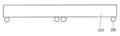
도 1에 도시된 바와 같이, 상부의 메모리 패키지(100)는, PCB 기판(110) 상에 다수의 메모리 반도체 칩(120, 130)이 칩 온 칩(Chip on Chip)에 의하여 상하로 적층(Stack) 되어 있다. 상기 실시예의 경우에는 동일 메모리의 반도체 칩의 경우을 설명하고 있으나, 메모리 패키지에 이종 메모리 반도체 칩이 적층(Stack)될 수 있음을 배제하지 않는다.As shown in FIG. 1, in the
각 반도체 칩(120, 130)은 PCB 기판(110)과 와이어(140) 본딩(bonding) 됨으로써 전기적으로 상호 연결(interconnection) 되고, 기판(110)의 하부에 솔더 볼(150)이 형성됨으로써 외부와 전기적으로 연결된다. 상기 기판(110) 상에는 반도체 칩(120, 130)과 와이어(140)를 보호하는 보호부재(160)가 몰딩되어 있다.Each of the
한편 도 1은, 상부의 메모리 패키지(100)가 하부의 로직 패키지(200)와 패키지 온 패키지(Package on Package)에 의하여 연결되어 있음을 알 수 있다. 즉, 상부 기판(110)의 솔더 볼(150)은 하부 기판(210)의 볼 랜드(Ball land) 영역과 접착되어 장착된다.1 shows that the
상기 하부의 로직 패키지(200)는, PCB 기판(210) 상에 로직 반도체 칩(220)이 적층(Stack) 되는 구조로 되어 있다. 마찬가지로 로직 반도체 칩(220)은 와이어(240) 본딩에 의하여 연결되고, 보호부재(260)에 의하여 몰딩되어 있다. 도면에는 도시되어 있지 않지만, 하부 PCB 기판(210)에는 다수의 비아(도시되지 않음)가 형성된다. 비아에는 반도체 칩(220)이 외부 모듈 기판과 연결되는 도전부재(도시되지 않음)가 충진된다. 그리고, 하부 솔더 볼(250)을 통하여 외부 모듈 기판과 접촉된다.The
따라서, 패키지 시스템 내에 다수의 반도체 칩이 적층(Stack) 됨으로서, 실장 면적의 증가를 억제하는 작용효과가 기대된다.Therefore, by stacking a plurality of semiconductor chips in the package system, the effect of suppressing the increase in the mounting area is expected.
그러나, 위와 같은 칩 온 칩(Chip on Chip) 방식의 반도체 칩의 적층 구조에 의하면, 기판(110) 상에 기판과 성질을 달리하는 동종 혹은 이종 반도체 칩(120, 130)이 적층됨으로써, 기판(110) 혹은 반도체 칩(120, 130)이 휘거나 변형되는 휨(Warpage) 현상이 발생한다. 더 나아가 상기 반도체 칩을 각 패키지로 하여 패키지 온 패키지(Package on Package) 방식에 의하여 패키지를 적층할 때, 각 패키지 사이에 휨 현상으로 인하여 패키지 접촉 불량(non-wet)이 발생하는 한계가 있다.However, according to the stack structure of a chip on chip type semiconductor chip as described above, the same type or
예컨대, 반도체 칩의 열 팽창 계수(CTE)는 대략 3 내지 4 × 10⁻⁶/Co이고, PCB 기판의 열 팽창 계수(CTE)는 대략 15 내지 16 × 10-6/Co이기 때문에, 웨이퍼로 구성되는 반도체 칩(120, 130)과 합성수지로 구성되는 PCB 기판(110) 사이에는 열 팽창 계수(CTE)의 차이로 인하여 휨(Warpage) 현상이 두드러진다.For example, since the thermal expansion coefficient (CTE) of the semiconductor chip is about 3 to 4 × 10⁻⁶ / Co, and the thermal expansion coefficient (CTE) of the PCB substrate is about 15 to 16 × 10-6 / Co, it is composed of a wafer. The warpage phenomenon is prominent due to the difference in the coefficient of thermal expansion (CTE) between the
또한, 상부 솔더 볼(150)을 사이에 두고 상부 패키지(100)와 하부 패키지(200)가 결합되기 때문에, 솔더 볼(150)의 사이즈가 축소되는 경향이 있다. 따라서, 로직 반도체 칩(220)의 상하 실장 공간이 협소해지는 문제점이 있다. 무엇 보다도 상기한 적층 구조에서는 패키지 전체의 두께가 두꺼워질 수밖에 없다.In addition, since the
본 발명의 다른 실시예에 의하면, 도 2에 도시된 바와 같이 패키지의 부피를 최소화하기 위하여 패키지 온 패키지(Package on package) 방법에 의하여 상부 패키지(300)와 하부 패키지(400)를 상하로 적층(Stack)한다. 이때, 일실시예에서 기판을 PCB로 구성함으로써, 반도체 칩과의 열 팽창 계수의 차이로 인하여 휨 현상이 나타나는 점과, 솔더 볼의 접촉 불량 가능성이 높아지는 점과, 하부 반도체 칩이 기판 상에 형성됨으로써 전체 패키지의 높이가 높아지는 점을 고려해 볼 때, 기본적으로 반도체 칩이 실장되는 기판을 실리콘 웨이퍼로 구성하는 웨이퍼 레벨 패키지를 적용한다. 상, 하부 패키지(300, 400) 사이에 열 팽창 계수의 차이를 최소화하며, 솔더 볼 어태치(Solder ball attach) 능력을 강화하는데 중점을 두기로 한다.According to another embodiment of the present invention, in order to minimize the volume of the package as shown in Figure 2 by the package on package (Package on package) method by stacking the
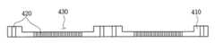
먼저, 상부 패키지(300)는, 웨이퍼 레벨에서 패키지를 제조하는 웨이퍼 패브리케이티드 패키지(Wafer fabricated package: WFP) 방법에 의한다.First, the
도 3에 도시된 바와 같이, 상부 기판(310) 상에 재배선 공정이 수행된다. 상부 기판(310)은, 적어도 실리콘을 포함하는 웨이퍼로 구성된다. 따라서, 웨이퍼 형태의 실리콘으로 구성된 상부 기판(310) 상에는 집적 회로와 다수의 입출력 패드(I/O Pad)(도시되지 않음)가 형성되어 있는 것은 물론이고, 재배선 공정에 의하여 재배선 레이어(도시되지 않음)가 증착된다. 상기 입출력 패드는 적층(Stack)될 반도체 칩과 와이어 본딩(W/B)에 의하여 전기적으로 연결되는 내부 접속 단자 기능을 수행하게 된다.As shown in FIG. 3, a redistribution process is performed on the
도 4에 도시된 바와 같이, 상기 재배선 공정이 이루어진 상부 기판(310) 상에는 하부 패키지(400)와 접속하기 위한 상부 도전부재(320)가 형성된다. 상부 도전부재(320)는, 솔더 볼 어태치(Solder ball attach) 공정에 의하여 상부 기판의 일측에 형성된다. 상기 솔더 볼은 상기 재배선 레이어를 매개로 상기 입출력 패드와 연결됨으로써 외부 접속 단자 기능을 수행하게 된다.As shown in FIG. 4, an upper
상기 솔더 볼 어태치 공정에 의하면, 리플로우(Reflow) 공정이 수반되는데, 열처리에 의하여 필연적으로 상부 기판이 휘어지는 웨이퍼 휨(wafer warpage) 현상이 발생하게 된다. 그러나, 본 발명의 실시예에 의하면, 상부 기판의 씨닝(thinning) 공정 전에 솔더 볼 어태치 공정이 선행하기 때문에 상대적으로 웨이퍼 휨 현상이 적게 나타나는 특징이 있다.According to the solder ball attach process, a reflow process is involved, which inevitably causes a wafer warpage phenomenon in which the upper substrate is bent by heat treatment. However, according to the exemplary embodiment of the present invention, since the solder ball attach process is preceded by the thinning process of the upper substrate, the wafer warpage phenomenon is relatively low.
도 5에 도시된 바와 같이, 상기 상부 기판(310)의 전면에 반도체 칩(330)이 적층(Stack)된다. 상기 반도체 칩(330)은 단일 메모리 반도체 칩으로 구성되거나 복수 메모리 반도체 칩으로 구성될 수 있다. 복수 메모리 반도체 칩으로 구성되는 경우에도 동종의 메모리 반도체 칩만으로 구성되거나 혹은 디램 혹은 프레쉬 메모리와 같이 이종 메모리 반도체 칩으로 구성될 수 있다.As shown in FIG. 5, the
상기 적층된 반도체 칩(310)과 입출력 패드(I/O Pad)를 전기적으로 연결하는 와이어(340) 본딩(W/B) 공정이 수행된다. 따라서, 입출력 패드에서 입력 패드(I Pad)가 와이어 본딩(W/B)에 의하여 반도체 칩(310)과 접속된다면, 출력 패드(O Pad)는 도전부재(320) 즉, 솔더 볼에 의하여 하부 패키지(400)와 접속된다.The
다만, 외부로부터 신호를 입력받거나 반대로 처리된 신호를 외부로 출력하는 입출력 패드의 순서는 동작에 따라 얼마든지 바뀔 수 있다. 상기 입출력 패드는 와이어 본딩 혹은 솔더 볼 중 어느 것이 적용되는냐에 따라, 본딩 핑거(bonding finger) 혹은 솔더 랜드(solder land)의 형태를 취할 수 있으며, 반드시 일정한 형태로 한정될 필요는 없다.However, the order of the input / output pads that receive a signal from the outside or output the processed signal to the outside may be changed depending on the operation. The input / output pad may take the form of a bonding finger or a solder land, depending on which wire bonding or solder ball is applied, and is not necessarily limited to a certain shape.
도 6에 도시된 바와 같이, 상부 기판(310)의 전면에 몰딩(Molding) 공정이 수행된다. 이로써, 에폭시 몰드 컴파운드(Epoxy Mold Compound)를 재료로 하는 상부 보호부재(350)가 형성된다. 상기 에폭시 몰드 컴파운드의 두께는 상기 직접회로나 와이어 본딩을 포함하여 웨이퍼 전면을 보호할 수 있을 정도로 형성되되, 솔더 볼이 메몰되지 않아야 한다. 가령, 솔더 볼이 절반 이상 메몰되되, 적어도 일부가 외부로 노출되는 정도로 형성되어야 한다. 본 발명의 실시예에 의하면, 에폭시 몰드 컴파운드는 도전부재(320)를 상부 기판(310) 상에 견고하게 고정하는 역할을 수행한다.As shown in FIG. 6, a molding process is performed on the entire surface of the
즉 솔더 볼은 1차적으로 리플로우에 의하여 상부 기판 상에 고정되지만, 항상 솔더 접촉 신뢰도(Solder joint reliability)가 저하되는 경향에 있기 때문에 접촉 불량(non-wet)의 문제가 항상 제기된다. 따라서, 솔더 볼의 고정력을 더욱 강화하기 위하여, 솔더 볼의 일부만 노출되고 나머지 부분은 메몰되도록 몰딩함으로써 솔더 볼의 고정력을 획기적으로 개선한다. 이로써, 솔더 접촉 신뢰도를 근복적으로 향상시킬 수 있게 된다.That is, the solder ball is first fixed on the upper substrate by reflow, but the problem of non-wet is always raised because solder joint reliability tends to be lowered. Therefore, in order to further strengthen the fixing force of the solder ball, the fixing force of the solder ball is drastically improved by molding so that only a part of the solder ball is exposed and the remaining part is buried. As a result, the solder contact reliability can be improved in recent years.
다만, 솔더 볼의 용융점이 250℃ 정도인 점을 고려하여, 몰딩 적정 온도는 170℃ 내지 180℃ 정도에서 결정할 수 있다.However, in consideration of the melting point of the solder ball is about 250 ℃, the molding appropriate temperature can be determined at about 170 ℃ to 180 ℃.
도 7에 도시된 바와 같이, 상부 기판(310)의 배면을 백 랩(Back-lap)함으로써, 씨닝 공정이 수행된다. 적층된 반도체 패키지의 높이를 최소화하기 위하여, 웨이퍼의 배면을 일정한 두께로 연마하는 것이다. 이때, 본 발명의 실시예에 의하면, 에폭시 몰드 컴파운드의 보호부재(350)에 의하여 상부 기판(310)의 전면이 지지되고 있기 때문에, 상부 기판의 배면이 소정 두께로 얇아지더라도 상부 기판이 휘어지거나 하는 문제는 발생하지 않는다.As shown in FIG. 7, the thinning process is performed by back-laping the back surface of the
도 8에 도시된 바와 같이, 백 랩된 웨이퍼 기판(310)의 배면에 상기 베어 웨이퍼를 보호하기 위한 지지부재(360)를 보호필름(370)을 이용하여 부착한다. 마지막으로, 싱글레이션(Singlation) 공정에 의하여 낱개로 절단되고, 각 개별 패키지는 지지부재(360)로부터 쉽게 분리되어, 후속의 패키지 온 패키지 공정에 이용된다.As shown in FIG. 8, a
여기서, '상부' 혹은 '하부', '전면 혹은 배면'은 어디까지나 상대적인 개념인 것이고, 도면을 기준으로 각 구성요소 상호간의 상대적인 위치를 이해하기 쉽게 식별하기 위한 것에 지나지 않으며, 각 위치와 방향을 한정하기 위한 것이 아님은 너무 명백하다.Here, 'upper' or 'lower', 'front or back' is a relative concept to the last, and it is merely to easily identify the relative positions of each component based on the drawings, and to identify each position and direction. It is too obvious to be limiting.
다음, 하부 패키지(400)는 반도체 칩이 기판에 삽입되는 내장형 반도체 패키지 제조방법에 의한다.Next, the
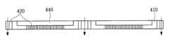
도 9에 도시된 바와 같이, 하부 기판(410) 상에 재배선 공정과 쓰루 실리콘 비아 공정이 동시에 혹은 순차적으로 진행된다. 하부 기판(410)은 상부 기판(310)과 마찬가지로, 적어도 실리콘을 포함하는 웨이퍼로 구성된다. 하부 기판(410)에 는 상부 기판(310)에서와 같이 집적 회로와 같은 패턴이 별도로 형성되지는 않는다.As shown in FIG. 9, the redistribution process and the through silicon via process are simultaneously or sequentially performed on the
다만, 하부 기판(410)의 전면에는 쓰루 실리콘 비아(420)에 의하여 후술할 내장 반도체 칩을 외부 기판 모듈과 전기적으로 연결할 다수의 입출력 패드(I/O Pad)(도시되지 않음)가 형성되고, 재배선 공정에 의하여 재배선 레이어(도시되지 않음)가 증착된다. 상기 입출력 패드는 외부의 기판과 전기적으로 연결되는 내부 접속 단자 기능을 수행하게 된다.However, a plurality of I / O pads (not shown) are formed on the front surface of the
도 10에 도시된 바와 같이, 하부 기판의 배면을 백랩하여 기판의 두께를 씨닝한다. 그리고 상기 쓰루 실리콘 비아(420)와 대응되는 기판(410)의 배면에는 캐비티(430)를 형성한다. 캐비티(430)는, 탑재될 반도체 칩이 외부로 돌출되지 않고 메몰되되, 최소한의 깊이로 형성된다. 상기 캐비티 형성방법은, 플라즈마 식각(Plasma Ehthing)에 의한다.As shown in FIG. 10, the thickness of the substrate is thinned by back wrapping the bottom surface of the lower substrate. A
여기서, 하부 기판(410)이 상부 기판(310)과 구별되는 것은, 하부 기판(410)에는 다수의 쓰루 실리콘 비아(420)가 형성되어 있다는 점이다. 이는 기판 내부에 로직 회로의 반도체 칩을 내장하기 위한 것이다. 즉, 하부 기판의 배면에는 반도체 칩을 내장할 수 있는 캐비티(430)가 형성되고, 상기 캐비티에 의하여 반도체 칩이 안착되는 캐비티 부분에는 전술한 다수의 쓰루 실리콘 비아(420)가 형성된다.Here, the
한편, 쓰루 실리콘 비아(420)는, 기판과 반도체 칩을 내부적으로 연결하기 위한 칩 스택용 비아와, 기판과 기판을 외부적으로 연결하기 위한 패키지 스택용 비아로 나누어 구성될 수 있다. 따라서, 칩 스택용 비아는 장착될 반도체 칩의 다 수 핀과 대응되게 형성되며, 패키지 스택용 비아는 반도체 칩과 대응되지 않는 주변 영역에 형성되는 것이 바람직하다.The through silicon via 420 may be divided into a chip stack via for internally connecting the substrate and the semiconductor chip, and a package stack via for externally connecting the substrate and the substrate. Therefore, the chip stack via is formed to correspond to a plurality of pins of the semiconductor chip to be mounted, and the package stack via is preferably formed in a peripheral area not corresponding to the semiconductor chip.
특히, 본 발명의 다른 실시예에서 캐비티(430)를 형성하고, 캐비티와 대응되는 기판 상에 비아(420)를 형성하는 것은, 로직 반도체 칩은 메모리 반도체 칩과 구별되는 다수의 핀이 형성되어 있기 때문이다. 다수의 핀은 와이어 본딩으로 접속하기 적합하지 않다. 따라서, 다수의 핀을 전기적으로 연결하는데는 비아(420)가 적합하고, 이를 위하여 반도체 칩이 탑재될 캐비티가 요구되는 것이다. 또한 와이어 본딩에 비하여 비아에 의한 접속의 경우에는 실장 면적이 축소되는 장점이 있기 때문이다.In particular, in another embodiment of the present invention, the
상기 비아(420)의 형성방법은, 건식 에칭(Dry Ehthing)에 의하여 형성되는 것이 바람직하지만, 반드시 이에 제한되는 것은 아니다. 기타 레이저 가공 등의 방법에 의할 수 있다. PCB 기판의 경우에는 에칭에 의한 비아 형성이 용이하지 않는데 반하여, 웨이퍼 기판에서는 레이저 가공 방법은 물론이고, 그 밖에 에칭 등의 방법에 의하여 비아를 형성하기 용이한 잇점이 있다. 상기 비아(420)에는 도전성의 금이나 구리와 같은 금속이 도금 혹은 증착된다.The via 420 may be formed by dry etching, but is not necessarily limited thereto. And other laser processing methods. In the case of a PCB substrate, via formation by etching is not easy. On the other hand, in the wafer substrate, not only the laser processing method but also the via formation is easily performed by etching or the like. The via 420 is plated or deposited with a conductive metal such as gold or copper.
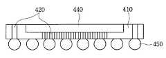
도 11에 도시된 바와 같이, 캐비티(430)가 형성되었다면, 반도체 칩이 기판의 내부에 탑재되는 형태로 기판 상에 로직 반도체 칩(440)을 적층(Stack) 한다. 전술한 바와 같이, 반도체 칩의 핀이 상기 비아와 적절하게 대응되도록 설치하여야 한다.As illustrated in FIG. 11, when the
도 12에 도시된 바와 같이, 소잉 공정을 통하여 개개의 반도체 패키지(400) 로 분리된다. 소잉 공정을 수행하기 전에 후술할 솔더 볼 어태치 공정을 먼저 진행할 수 있다.As shown in FIG. 12, the
도 13에 도시된 바와 같이, 재배선 공정이 이루어진 하부 기판(410)의 전면에는 외부 기판 모듈과 접속하기 위한 하부 도전부재(450)가 형성된다. 하부 도전부재(450)는, 솔더 볼 어태치(Solder ball attach) 공정에 의하여 형성되는 솔더 볼로 구성된다. 상기 솔더 볼은 상기 재배선 레이어를 매개로 상기 입출력 패드와 연결됨으로써 외부 접속 단자 기능을 수행하게 된다.As shown in FIG. 13, a lower
위와 같은 방법으로, 하부 패키지(400)가 완성되면, 최종적으로 준비된 상부 패키지(300)와 하부 패키지(400)를 수직으로 적층하는 패키지 온 패키지 공정을 수행한다. 다만, 상부 패키지(300)의 전면이 하부 패키지(400)의 배면과 마주봄으로써, 상부 웨이퍼 기판의 하부로 반도체 칩이 적층(Stack) 되는 구조를 갖게 된다.In the same manner as above, when the
상부 패키지의 상부 도전부재(320)는 하부 패키지의 하부 도전부재(450)와 패키지 스택용 비아(420)를 매개로 하여 전기적으로 연결된다.The upper
이와 같이, 상, 하부 패키지(300, 400)를 솔더 볼에 의하여 접합하게 되면, 상,하부 기판(310, 410) 상호간의 동일한 열 팽창 계수로 인하여 혹은 기판(310, 410)과 반도체 칩(330, 440) 상호간의 동일한 열 팽창 계수로 인하여, 휨 현상이 최소화되고, 외부의 충격에도 패키지가 쉽게 데미지를 입지 않게 된다.As such, when the upper and
이상에서 살펴본 바와 같이, 본 발명의 상부 메모리 반도체 칩 패키지는, 열 팽창 계수의 차이로 인한 휨 현상을 최소화하기 위하여, 실리콘 웨이퍼를 기판으로 하여 반도체 칩을 실장하고, 동시에 솔더 볼의 어태치 능력을 강화하기 위하여, 반 도체 칩이 구비되는 기판 상에 에폭시를 몰딩하되, 솔더 볼의 일부가 노출되도록 하는 칩 스택에 관한 것이다. 또한 본 발명의 하부 로직 반도체 칩 패키지는, 실장 면적을 최소화하면서도 적층 두께를 제한하기 위하여, 로직 메모리 반도체 칩을 실리콘 웨이퍼 레벨에서 실장하되, 다수의 비아가 형성된 캐비티에 반도체 칩을 삽입하고, 다수의 핀을 비아와 접속시키는 칩 스택에 관한 것이다. 이로써, 본 발명은 상부 메모리 반도체 칩 패키지에서 반도체 칩과 솔더 볼이 구비된 기판의 전면이 하부를 향하도록 배치하고, 하부 메모리 반도체 칩 패키지에서 패키지에 삽입된 반도체 칩이 상부를 향하도록 배치하는 패키지 스택에 관한 구성을 기술적 사상으로 하고 있음을 알 수 있다. 이와 같은 본 발명의 기본적인 기술적 사상의 범주 내에서, 당업계의 통상의 지식을 가진 자에게 있어서는 다른 많은 변형이 가능할 것이다.As described above, the upper memory semiconductor chip package of the present invention mounts the semiconductor chip using a silicon wafer as a substrate and minimizes the attaching ability of the solder balls in order to minimize warpage due to a difference in thermal expansion coefficient. To reinforce, the present invention relates to a chip stack in which an epoxy is molded on a substrate on which a semiconductor chip is provided, but a portion of the solder balls is exposed. In addition, the lower logic semiconductor chip package of the present invention, in order to limit the thickness of the stack while minimizing the mounting area, the logic memory semiconductor chip is mounted at the silicon wafer level, the semiconductor chip is inserted into a cavity having a plurality of vias, A chip stack connects pins with vias. Accordingly, the present invention is a package in which the front surface of the substrate with the semiconductor chip and the solder ball in the upper memory semiconductor chip package is disposed downward, and the semiconductor chip inserted into the package in the lower memory semiconductor chip package facing upward It can be seen that the configuration of the stack is a technical idea. Within the scope of the basic technical idea of the present invention, many other modifications will be possible to those skilled in the art.
도 1은 본 발명의 일실시예에 의한 패키지 온 패키지 구성을 나타내는 단면도.1 is a cross-sectional view showing a package on package configuration according to an embodiment of the present invention.
도 2는 본 발명의 다른 실시예에 의한 패키지 온 패키지 구성을 나타내는 단면도.2 is a cross-sectional view showing a package on package configuration according to another embodiment of the present invention.
도 3은 본 발명에 의한 상부 패키지의 재배선 공정을 나타내는 단면도.Figure 3 is a cross-sectional view showing a rewiring process of the upper package according to the present invention.
도 4는 본 발명에 의한 상부 패키지의 솔더 볼 어태치 공정을 나타내는 단면도.Figure 4 is a cross-sectional view showing a solder ball attach process of the upper package according to the present invention.
도 5는 본 발명에 의한 상부 패키지의 칩 스택 공정을 나타내는 단면도.Figure 5 is a cross-sectional view showing a chip stack process of the upper package according to the present invention.
도 6은 본 발명에 의한 상부 패키지의 몰딩 공정을 나타내는 단면도.6 is a sectional view showing a molding process of the upper package according to the present invention.
도 7은 본 발명에 의한 상부 패키지의 씨닝 공정을 나타내는 단면도.Figure 7 is a cross-sectional view showing a thinning step of the upper package according to the present invention.
도 8은 본 발명에 의한 상부 패키지의 싱글에이션 공정을 나타내는 단면도.8 is a cross-sectional view showing a singulation process of the upper package according to the present invention.
도 9는 본 발명에 의한 하부 패키지의 재배선 공정 및 쓰루 비아 공정을 나타내는 단면도.Figure 9 is a cross-sectional view showing a redistribution process and through via process of the lower package according to the present invention.
도 10은 본 발명에 의한 하부 패키지의 씨닝 공정 및 캐비티 공정을 나타내는 단면도.10 is a cross-sectional view showing a thinning step and a cavity step of a lower package according to the present invention.
도 11은 본 발명에 의한 하부 패키지의 칩 스택 공정을 나타내는 단면도.11 is a cross-sectional view showing a chip stack process of a lower package according to the present invention.
도 12는 본 발명에 의한 하부 패키지의 싱글레이션 공정을 나타내는 단면도.12 is a cross-sectional view showing a singulation process of a lower package according to the present invention.
도 13은 본 발명에 의한 하부 패키지의 솔더 볼 어태치 공정을 나타내는 단면도.Figure 13 is a cross-sectional view showing a solder ball attach process of the lower package according to the present invention.
**도면의 주요구성에 대한 부호의 설명**** Description of Codes for Major Configurations of Drawings **
100: 메모리 패키지100: PCB 기판100: memory package 100: PCB substrate
120, 130: 반도체 칩140: 와이어120, 130: semiconductor chip 140: wire
150: 솔더 볼160: 보호부재150: solder ball 160: protective member
200: 로직 패키지210: PCB 기판200: logic package 210: PCB substrate
220: 반도체 칩240: 와이어220: semiconductor chip 240: wire
250: 솔더 볼260: 보호부재250: solder ball 260: protective member
300: 상부 패키지310: 실리콘 웨이퍼 기판300: upper package 310: silicon wafer substrate
320: 도전부재330: 반도체 칩320: conductive member 330: semiconductor chip
340: 와이어350: 보호부재340: wire 350: protective member
360: 지지부재370: 보호필름360: support member 370: protective film
400: 하부 패키지410: 실리콘 웨이퍼 기판400: lower package 410: silicon wafer substrate
420: 비아430: 캐비티420: Via 430: Cavity
440: 반도체 칩450: 도전부재440: semiconductor chip 450: conductive member
Claims (19)
Translated fromKoreanPriority Applications (2)
| Application Number | Priority Date | Filing Date | Title |
|---|---|---|---|
| KR1020080109802AKR101461630B1 (en) | 2008-11-06 | 2008-11-06 | Wafer level chip on chip package, package on package improving solder joint reliability but reducing mounting height and manufacturing method thereof |
| US12/612,022US8143710B2 (en) | 2008-11-06 | 2009-11-04 | Wafer-level chip-on-chip package, package on package, and methods of manufacturing the same |
Applications Claiming Priority (1)
| Application Number | Priority Date | Filing Date | Title |
|---|---|---|---|
| KR1020080109802AKR101461630B1 (en) | 2008-11-06 | 2008-11-06 | Wafer level chip on chip package, package on package improving solder joint reliability but reducing mounting height and manufacturing method thereof |
Publications (2)
| Publication Number | Publication Date |
|---|---|
| KR20100050750Atrue KR20100050750A (en) | 2010-05-14 |
| KR101461630B1 KR101461630B1 (en) | 2014-11-20 |
Family
ID=42130381
Family Applications (1)
| Application Number | Title | Priority Date | Filing Date |
|---|---|---|---|
| KR1020080109802AActiveKR101461630B1 (en) | 2008-11-06 | 2008-11-06 | Wafer level chip on chip package, package on package improving solder joint reliability but reducing mounting height and manufacturing method thereof |
Country Status (2)
| Country | Link |
|---|---|
| US (1) | US8143710B2 (en) |
| KR (1) | KR101461630B1 (en) |
Cited By (11)
| Publication number | Priority date | Publication date | Assignee | Title |
|---|---|---|---|---|
| WO2017066239A1 (en)* | 2015-10-12 | 2017-04-20 | Invensas Corporation | Embedded wire bond wires |
| US9812402B2 (en) | 2015-10-12 | 2017-11-07 | Invensas Corporation | Wire bond wires for interference shielding |
| US9852969B2 (en) | 2013-11-22 | 2017-12-26 | Invensas Corporation | Die stacks with one or more bond via arrays of wire bond wires and with one or more arrays of bump interconnects |
| US9888579B2 (en) | 2015-03-05 | 2018-02-06 | Invensas Corporation | Pressing of wire bond wire tips to provide bent-over tips |
| US9953914B2 (en) | 2012-05-22 | 2018-04-24 | Invensas Corporation | Substrate-less stackable package with wire-bond interconnect |
| US10008469B2 (en) | 2015-04-30 | 2018-06-26 | Invensas Corporation | Wafer-level packaging using wire bond wires in place of a redistribution layer |
| US10026717B2 (en) | 2013-11-22 | 2018-07-17 | Invensas Corporation | Multiple bond via arrays of different wire heights on a same substrate |
| KR20190049328A (en)* | 2017-11-01 | 2019-05-09 | 박경화 | Recycling method for semiconductor package, recycling semiconductor package and jig for the same |
| US11189595B2 (en) | 2011-10-17 | 2021-11-30 | Invensas Corporation | Package-on-package assembly with wire bond vias |
| US11404338B2 (en) | 2014-01-17 | 2022-08-02 | Invensas Corporation | Fine pitch bva using reconstituted wafer with area array accessible for testing |
| US11424211B2 (en) | 2011-05-03 | 2022-08-23 | Tessera Llc | Package-on-package assembly with wire bonds to encapsulation surface |
Families Citing this family (73)
| Publication number | Priority date | Publication date | Assignee | Title |
|---|---|---|---|---|
| KR101313391B1 (en) | 2004-11-03 | 2013-10-01 | 테세라, 인코포레이티드 | Stacked packaging improvements |
| US8058101B2 (en) | 2005-12-23 | 2011-11-15 | Tessera, Inc. | Microelectronic packages and methods therefor |
| US7963369B2 (en)* | 2007-01-26 | 2011-06-21 | Werner Co. | Step stool and method |
| US9219023B2 (en)* | 2010-01-19 | 2015-12-22 | Globalfoundries Inc. | 3D chip stack having encapsulated chip-in-chip |
| KR20110133945A (en)* | 2010-06-08 | 2011-12-14 | 삼성전자주식회사 | Stacked package and its manufacturing method |
| US8482111B2 (en) | 2010-07-19 | 2013-07-09 | Tessera, Inc. | Stackable molded microelectronic packages |
| US9159708B2 (en) | 2010-07-19 | 2015-10-13 | Tessera, Inc. | Stackable molded microelectronic packages with area array unit connectors |
| US8754516B2 (en) | 2010-08-26 | 2014-06-17 | Intel Corporation | Bumpless build-up layer package with pre-stacked microelectronic devices |
| KR101075241B1 (en) | 2010-11-15 | 2011-11-01 | 테세라, 인코포레이티드 | Microelectronic package with terminals in dielectric member |
| US20120146206A1 (en) | 2010-12-13 | 2012-06-14 | Tessera Research Llc | Pin attachment |
| KR101817159B1 (en) | 2011-02-17 | 2018-02-22 | 삼성전자 주식회사 | Semiconductor package having TSV interposer and method of manufacturing the same |
| US9164679B2 (en) | 2011-04-06 | 2015-10-20 | Patents1, Llc | System, method and computer program product for multi-thread operation involving first memory of a first memory class and second memory of a second memory class |
| US9170744B1 (en) | 2011-04-06 | 2015-10-27 | P4tents1, LLC | Computer program product for controlling a flash/DRAM/embedded DRAM-equipped system |
| US9176671B1 (en) | 2011-04-06 | 2015-11-03 | P4tents1, LLC | Fetching data between thread execution in a flash/DRAM/embedded DRAM-equipped system |
| US8930647B1 (en) | 2011-04-06 | 2015-01-06 | P4tents1, LLC | Multiple class memory systems |
| US9158546B1 (en) | 2011-04-06 | 2015-10-13 | P4tents1, LLC | Computer program product for fetching from a first physical memory between an execution of a plurality of threads associated with a second physical memory |
| US9432298B1 (en) | 2011-12-09 | 2016-08-30 | P4tents1, LLC | System, method, and computer program product for improving memory systems |
| US8618659B2 (en) | 2011-05-03 | 2013-12-31 | Tessera, Inc. | Package-on-package assembly with wire bonds to encapsulation surface |
| US8552518B2 (en)* | 2011-06-09 | 2013-10-08 | Optiz, Inc. | 3D integrated microelectronic assembly with stress reducing interconnects |
| KR20130007049A (en)* | 2011-06-28 | 2013-01-18 | 삼성전자주식회사 | Package on package using through silicon via technique |
| US9417754B2 (en) | 2011-08-05 | 2016-08-16 | P4tents1, LLC | User interface system, method, and computer program product |
| US9054098B2 (en)* | 2011-08-30 | 2015-06-09 | Stats Chippac Ltd. | Integrated circuit packaging system with redistribution layer and method of manufacture thereof |
| US8946757B2 (en) | 2012-02-17 | 2015-02-03 | Invensas Corporation | Heat spreading substrate with embedded interconnects |
| US8372741B1 (en) | 2012-02-24 | 2013-02-12 | Invensas Corporation | Method for package-on-package assembly with wire bonds to encapsulation surface |
| US9349706B2 (en) | 2012-02-24 | 2016-05-24 | Invensas Corporation | Method for package-on-package assembly with wire bonds to encapsulation surface |
| US9263412B2 (en) | 2012-03-09 | 2016-02-16 | Taiwan Semiconductor Manufacturing Company, Ltd. | Packaging methods and packaged semiconductor devices |
| US20130234317A1 (en) | 2012-03-09 | 2013-09-12 | Taiwan Semiconductor Manufacturing Company, Ltd. | Packaging Methods and Packaged Semiconductor Devices |
| KR101947722B1 (en)* | 2012-06-07 | 2019-04-25 | 삼성전자주식회사 | stack semiconductor package and method of manufacturing the same |
| TWI470688B (en)* | 2012-07-18 | 2015-01-21 | Alpha & Omega Semiconductor Cayman Ltd | Wafer level chip scale semiconductor package and method thereof |
| US9391008B2 (en) | 2012-07-31 | 2016-07-12 | Invensas Corporation | Reconstituted wafer-level package DRAM |
| US9502390B2 (en) | 2012-08-03 | 2016-11-22 | Invensas Corporation | BVA interposer |
| US8975738B2 (en) | 2012-11-12 | 2015-03-10 | Invensas Corporation | Structure for microelectronic packaging with terminals on dielectric mass |
| US8878353B2 (en) | 2012-12-20 | 2014-11-04 | Invensas Corporation | Structure for microelectronic packaging with bond elements to encapsulation surface |
| US9136254B2 (en) | 2013-02-01 | 2015-09-15 | Invensas Corporation | Microelectronic package having wire bond vias and stiffening layer |
| US9034696B2 (en) | 2013-07-15 | 2015-05-19 | Invensas Corporation | Microelectronic assemblies having reinforcing collars on connectors extending through encapsulation |
| US9023691B2 (en) | 2013-07-15 | 2015-05-05 | Invensas Corporation | Microelectronic assemblies with stack terminals coupled by connectors extending through encapsulation |
| US8883563B1 (en) | 2013-07-15 | 2014-11-11 | Invensas Corporation | Fabrication of microelectronic assemblies having stack terminals coupled by connectors extending through encapsulation |
| US9167710B2 (en) | 2013-08-07 | 2015-10-20 | Invensas Corporation | Embedded packaging with preformed vias |
| US9685365B2 (en) | 2013-08-08 | 2017-06-20 | Invensas Corporation | Method of forming a wire bond having a free end |
| US20150076714A1 (en) | 2013-09-16 | 2015-03-19 | Invensas Corporation | Microelectronic element with bond elements to encapsulation surface |
| US9087815B2 (en) | 2013-11-12 | 2015-07-21 | Invensas Corporation | Off substrate kinking of bond wire |
| US9082753B2 (en) | 2013-11-12 | 2015-07-14 | Invensas Corporation | Severing bond wire by kinking and twisting |
| US9263394B2 (en) | 2013-11-22 | 2016-02-16 | Invensas Corporation | Multiple bond via arrays of different wire heights on a same substrate |
| US9214454B2 (en) | 2014-03-31 | 2015-12-15 | Invensas Corporation | Batch process fabrication of package-on-package microelectronic assemblies |
| US10381326B2 (en) | 2014-05-28 | 2019-08-13 | Invensas Corporation | Structure and method for integrated circuits packaging with increased density |
| US9646917B2 (en) | 2014-05-29 | 2017-05-09 | Invensas Corporation | Low CTE component with wire bond interconnects |
| US9412714B2 (en) | 2014-05-30 | 2016-08-09 | Invensas Corporation | Wire bond support structure and microelectronic package including wire bonds therefrom |
| US9548289B2 (en) | 2014-09-15 | 2017-01-17 | Mediatek Inc. | Semiconductor package assemblies with system-on-chip (SOC) packages |
| US9679842B2 (en) | 2014-10-01 | 2017-06-13 | Mediatek Inc. | Semiconductor package assembly |
| US9735084B2 (en) | 2014-12-11 | 2017-08-15 | Invensas Corporation | Bond via array for thermal conductivity |
| US9761554B2 (en) | 2015-05-07 | 2017-09-12 | Invensas Corporation | Ball bonding metal wire bond wires to metal pads |
| US10332854B2 (en) | 2015-10-23 | 2019-06-25 | Invensas Corporation | Anchoring structure of fine pitch bva |
| US10181457B2 (en) | 2015-10-26 | 2019-01-15 | Invensas Corporation | Microelectronic package for wafer-level chip scale packaging with fan-out |
| US10043779B2 (en) | 2015-11-17 | 2018-08-07 | Invensas Corporation | Packaged microelectronic device for a package-on-package device |
| US9659848B1 (en) | 2015-11-18 | 2017-05-23 | Invensas Corporation | Stiffened wires for offset BVA |
| US9984992B2 (en) | 2015-12-30 | 2018-05-29 | Invensas Corporation | Embedded wire bond wires for vertical integration with separate surface mount and wire bond mounting surfaces |
| US9935075B2 (en) | 2016-07-29 | 2018-04-03 | Invensas Corporation | Wire bonding method and apparatus for electromagnetic interference shielding |
| US10299368B2 (en) | 2016-12-21 | 2019-05-21 | Invensas Corporation | Surface integrated waveguides and circuit structures therefor |
| JP2018117102A (en)* | 2017-01-20 | 2018-07-26 | ソニーセミコンダクタソリューションズ株式会社 | Semiconductor device |
| US10593647B2 (en)* | 2018-06-27 | 2020-03-17 | Powertech Technology Inc. | Package structure and manufacturing method thereof |
| KR102582422B1 (en) | 2018-06-29 | 2023-09-25 | 삼성전자주식회사 | Semiconductor Package having Redistribution layer |
| CN109003961B (en)* | 2018-07-26 | 2020-06-16 | 华进半导体封装先导技术研发中心有限公司 | 3D system integrated structure and manufacturing method thereof |
| US11171115B2 (en) | 2019-03-18 | 2021-11-09 | Kepler Computing Inc. | Artificial intelligence processor with three-dimensional stacked memory |
| US11836102B1 (en) | 2019-03-20 | 2023-12-05 | Kepler Computing Inc. | Low latency and high bandwidth artificial intelligence processor |
| US12079475B1 (en) | 2019-05-31 | 2024-09-03 | Kepler Computing Inc. | Ferroelectric memory chiplet in a multi-dimensional packaging |
| US12086410B1 (en) | 2019-05-31 | 2024-09-10 | Kepler Computing Inc. | Ferroelectric memory chiplet in a multi-dimensional packaging with I/O switch embedded in a substrate or interposer |
| US11844223B1 (en) | 2019-05-31 | 2023-12-12 | Kepler Computing Inc. | Ferroelectric memory chiplet as unified memory in a multi-dimensional packaging |
| US11043472B1 (en) | 2019-05-31 | 2021-06-22 | Kepler Compute Inc. | 3D integrated ultra high-bandwidth memory |
| US10964616B2 (en)* | 2019-06-17 | 2021-03-30 | Advanced Semiconductor Engineering, Inc. | Semiconductor package structure and method of manufacturing the same |
| US11251119B2 (en)* | 2019-09-25 | 2022-02-15 | Taiwan Semiconductor Manufacturing Company, Ltd. | Package structure, package-on-package structure and method of fabricating the same |
| CN111769088B (en)* | 2020-09-03 | 2021-01-01 | 浙江集迈科微电子有限公司 | Stacking packaging structure based on back liquid cooling import and preparation method thereof |
| CN114664333A (en)* | 2021-03-26 | 2022-06-24 | 深圳宏芯宇电子股份有限公司 | Dynamic random access memory and processor module |
| US11791233B1 (en) | 2021-08-06 | 2023-10-17 | Kepler Computing Inc. | Ferroelectric or paraelectric memory and logic chiplet with thermal management in a multi-dimensional packaging |
Family Cites Families (11)
| Publication number | Priority date | Publication date | Assignee | Title |
|---|---|---|---|---|
| KR0179921B1 (en)* | 1996-05-17 | 1999-03-20 | 문정환 | Stacked semiconductor package |
| KR100260997B1 (en)* | 1998-04-08 | 2000-07-01 | 마이클 디. 오브라이언 | Semiconductor package |
| KR20010027266A (en) | 1999-09-13 | 2001-04-06 | 윤종용 | Stack package |
| US6344401B1 (en) | 2000-03-09 | 2002-02-05 | Atmel Corporation | Method of forming a stacked-die integrated circuit chip package on a water level |
| US20020074652A1 (en)* | 2000-12-15 | 2002-06-20 | Pierce John L. | Method, apparatus and system for multiple chip assemblies |
| US20070141751A1 (en)* | 2005-12-16 | 2007-06-21 | Mistry Addi B | Stackable molded packages and methods of making the same |
| US7659612B2 (en)* | 2006-04-24 | 2010-02-09 | Micron Technology, Inc. | Semiconductor components having encapsulated through wire interconnects (TWI) |
| KR20080006299A (en) | 2006-07-12 | 2008-01-16 | 한국광기술원 | Wafer-level packaged device and manufacturing method thereof |
| US7749882B2 (en)* | 2006-08-23 | 2010-07-06 | Micron Technology, Inc. | Packaged microelectronic devices and methods for manufacturing packaged microelectronic devices |
| US20080197469A1 (en)* | 2007-02-21 | 2008-08-21 | Advanced Chip Engineering Technology Inc. | Multi-chips package with reduced structure and method for forming the same |
| US8237259B2 (en)* | 2007-06-13 | 2012-08-07 | Infineon Technologies Ag | Embedded chip package |
- 2008
- 2008-11-06KRKR1020080109802Apatent/KR101461630B1/enactiveActive
- 2009
- 2009-11-04USUS12/612,022patent/US8143710B2/enactiveActive
Cited By (17)
| Publication number | Priority date | Publication date | Assignee | Title |
|---|---|---|---|---|
| US11424211B2 (en) | 2011-05-03 | 2022-08-23 | Tessera Llc | Package-on-package assembly with wire bonds to encapsulation surface |
| US11735563B2 (en) | 2011-10-17 | 2023-08-22 | Invensas Llc | Package-on-package assembly with wire bond vias |
| US11189595B2 (en) | 2011-10-17 | 2021-11-30 | Invensas Corporation | Package-on-package assembly with wire bond vias |
| US10510659B2 (en) | 2012-05-22 | 2019-12-17 | Invensas Corporation | Substrate-less stackable package with wire-bond interconnect |
| US9953914B2 (en) | 2012-05-22 | 2018-04-24 | Invensas Corporation | Substrate-less stackable package with wire-bond interconnect |
| USRE49987E1 (en) | 2013-11-22 | 2024-05-28 | Invensas Llc | Multiple plated via arrays of different wire heights on a same substrate |
| US9852969B2 (en) | 2013-11-22 | 2017-12-26 | Invensas Corporation | Die stacks with one or more bond via arrays of wire bond wires and with one or more arrays of bump interconnects |
| US10026717B2 (en) | 2013-11-22 | 2018-07-17 | Invensas Corporation | Multiple bond via arrays of different wire heights on a same substrate |
| US10629567B2 (en) | 2013-11-22 | 2020-04-21 | Invensas Corporation | Multiple plated via arrays of different wire heights on same substrate |
| US11404338B2 (en) | 2014-01-17 | 2022-08-02 | Invensas Corporation | Fine pitch bva using reconstituted wafer with area array accessible for testing |
| US9888579B2 (en) | 2015-03-05 | 2018-02-06 | Invensas Corporation | Pressing of wire bond wire tips to provide bent-over tips |
| US10008469B2 (en) | 2015-04-30 | 2018-06-26 | Invensas Corporation | Wafer-level packaging using wire bond wires in place of a redistribution layer |
| US10490528B2 (en) | 2015-10-12 | 2019-11-26 | Invensas Corporation | Embedded wire bond wires |
| WO2017066239A1 (en)* | 2015-10-12 | 2017-04-20 | Invensas Corporation | Embedded wire bond wires |
| US11462483B2 (en) | 2015-10-12 | 2022-10-04 | Invensas Llc | Wire bond wires for interference shielding |
| US9812402B2 (en) | 2015-10-12 | 2017-11-07 | Invensas Corporation | Wire bond wires for interference shielding |
| KR20190049328A (en)* | 2017-11-01 | 2019-05-09 | 박경화 | Recycling method for semiconductor package, recycling semiconductor package and jig for the same |
Also Published As
| Publication number | Publication date |
|---|---|
| US8143710B2 (en) | 2012-03-27 |
| US20100109138A1 (en) | 2010-05-06 |
| KR101461630B1 (en) | 2014-11-20 |
Similar Documents
| Publication | Publication Date | Title |
|---|---|---|
| KR101461630B1 (en) | Wafer level chip on chip package, package on package improving solder joint reliability but reducing mounting height and manufacturing method thereof | |
| US12033910B2 (en) | Wafer-level stack chip package and method of manufacturing the same | |
| US7326592B2 (en) | Stacked die package | |
| KR100895813B1 (en) | Manufacturing method of semiconductor package | |
| US8941225B2 (en) | Integrated circuit package and method for manufacturing the same | |
| US7429798B2 (en) | Integrated circuit package-in-package system | |
| KR100886100B1 (en) | Semiconductor package and manufacturing method thereof | |
| US8343803B2 (en) | Lightweight and compact through-silicon via stack package with excellent electrical connections and method for manufacturing the same | |
| US7589410B2 (en) | Molded reconfigured wafer, stack package using the same, and method for manufacturing the stack package | |
| KR101746731B1 (en) | Integrated circuit packaging stacking system with redistribution and method of manufacture thereof | |
| TWI482261B (en) | Three-dimensional system-in-package package-on-package structure | |
| US8089143B2 (en) | Integrated circuit package system using interposer | |
| US8026586B2 (en) | Semiconductor package | |
| KR20200024499A (en) | Stack package include bridge die | |
| KR20090004584A (en) | Semiconductor package and manufacturing method thereof | |
| CN111128914A (en) | Low-warpage multi-chip packaging structure and manufacturing method thereof | |
| US8097961B2 (en) | Semiconductor device having a simplified stack and method for manufacturing thereof | |
| CN110246812A (en) | A kind of semiconductor package and preparation method thereof | |
| KR101046253B1 (en) | Stacked chip semiconductor package using TS | |
| US7687920B2 (en) | Integrated circuit package-on-package system with central bond wires | |
| US20080237831A1 (en) | Multi-chip semiconductor package structure | |
| KR20090077580A (en) | Multi-chip package | |
| KR20110001182A (en) | Manufacturing method of semiconductor package | |
| KR101019705B1 (en) | Substrate for manufacturing semiconductor package and semiconductor package using same | |
| KR100650770B1 (en) | Flip chip double die package |
Legal Events
| Date | Code | Title | Description |
|---|---|---|---|
| PA0109 | Patent application | Patent event code:PA01091R01D Comment text:Patent Application Patent event date:20081106 | |
| PG1501 | Laying open of application | ||
| A201 | Request for examination | ||
| PA0201 | Request for examination | Patent event code:PA02012R01D Patent event date:20130304 Comment text:Request for Examination of Application Patent event code:PA02011R01I Patent event date:20081106 Comment text:Patent Application | |
| E902 | Notification of reason for refusal | ||
| PE0902 | Notice of grounds for rejection | Comment text:Notification of reason for refusal Patent event date:20140430 Patent event code:PE09021S01D | |
| E701 | Decision to grant or registration of patent right | ||
| PE0701 | Decision of registration | Patent event code:PE07011S01D Comment text:Decision to Grant Registration Patent event date:20140925 | |
| GRNT | Written decision to grant | ||
| PR0701 | Registration of establishment | Comment text:Registration of Establishment Patent event date:20141107 Patent event code:PR07011E01D | |
| PR1002 | Payment of registration fee | Payment date:20141110 End annual number:3 Start annual number:1 | |
| PG1601 | Publication of registration | ||
| FPAY | Annual fee payment | Payment date:20181031 Year of fee payment:5 | |
| PR1001 | Payment of annual fee | Payment date:20181031 Start annual number:5 End annual number:5 | |
| FPAY | Annual fee payment | Payment date:20191031 Year of fee payment:6 | |
| PR1001 | Payment of annual fee | Payment date:20191031 Start annual number:6 End annual number:6 | |
| PR1001 | Payment of annual fee | Payment date:20201030 Start annual number:7 End annual number:7 | |
| PR1001 | Payment of annual fee | Payment date:20211027 Start annual number:8 End annual number:8 |