KR20100022780A - Touch panel for display device - Google Patents
Touch panel for display deviceDownload PDFInfo
- Publication number
- KR20100022780A KR20100022780AKR1020080081454AKR20080081454AKR20100022780AKR 20100022780 AKR20100022780 AKR 20100022780AKR 1020080081454 AKR1020080081454 AKR 1020080081454AKR 20080081454 AKR20080081454 AKR 20080081454AKR 20100022780 AKR20100022780 AKR 20100022780A
- Authority
- KR
- South Korea
- Prior art keywords
- substrate
- upper substrate
- touch panel
- display device
- lower substrate
- Prior art date
- Legal status (The legal status is an assumption and is not a legal conclusion. Google has not performed a legal analysis and makes no representation as to the accuracy of the status listed.)
- Granted
Links
Images


Classifications
- G—PHYSICS
- G06—COMPUTING OR CALCULATING; COUNTING
- G06F—ELECTRIC DIGITAL DATA PROCESSING
- G06F3/00—Input arrangements for transferring data to be processed into a form capable of being handled by the computer; Output arrangements for transferring data from processing unit to output unit, e.g. interface arrangements
- G06F3/01—Input arrangements or combined input and output arrangements for interaction between user and computer
- G06F3/03—Arrangements for converting the position or the displacement of a member into a coded form
- G06F3/041—Digitisers, e.g. for touch screens or touch pads, characterised by the transducing means
- G06F3/0412—Digitisers structurally integrated in a display
- G—PHYSICS
- G02—OPTICS
- G02F—OPTICAL DEVICES OR ARRANGEMENTS FOR THE CONTROL OF LIGHT BY MODIFICATION OF THE OPTICAL PROPERTIES OF THE MEDIA OF THE ELEMENTS INVOLVED THEREIN; NON-LINEAR OPTICS; FREQUENCY-CHANGING OF LIGHT; OPTICAL LOGIC ELEMENTS; OPTICAL ANALOGUE/DIGITAL CONVERTERS
- G02F1/00—Devices or arrangements for the control of the intensity, colour, phase, polarisation or direction of light arriving from an independent light source, e.g. switching, gating or modulating; Non-linear optics
- G02F1/01—Devices or arrangements for the control of the intensity, colour, phase, polarisation or direction of light arriving from an independent light source, e.g. switching, gating or modulating; Non-linear optics for the control of the intensity, phase, polarisation or colour
- G02F1/13—Devices or arrangements for the control of the intensity, colour, phase, polarisation or direction of light arriving from an independent light source, e.g. switching, gating or modulating; Non-linear optics for the control of the intensity, phase, polarisation or colour based on liquid crystals, e.g. single liquid crystal display cells
- G02F1/133—Constructional arrangements; Operation of liquid crystal cells; Circuit arrangements
- G02F1/1333—Constructional arrangements; Manufacturing methods
- G—PHYSICS
- G06—COMPUTING OR CALCULATING; COUNTING
- G06F—ELECTRIC DIGITAL DATA PROCESSING
- G06F2203/00—Indexing scheme relating to G06F3/00 - G06F3/048
- G06F2203/041—Indexing scheme relating to G06F3/041 - G06F3/045
- G06F2203/04103—Manufacturing, i.e. details related to manufacturing processes specially suited for touch sensitive devices
Landscapes
- Physics & Mathematics (AREA)
- Engineering & Computer Science (AREA)
- Theoretical Computer Science (AREA)
- General Engineering & Computer Science (AREA)
- Nonlinear Science (AREA)
- General Physics & Mathematics (AREA)
- Optics & Photonics (AREA)
- Crystallography & Structural Chemistry (AREA)
- Chemical & Material Sciences (AREA)
- Human Computer Interaction (AREA)
- Mathematical Physics (AREA)
- Position Input By Displaying (AREA)
- Devices For Indicating Variable Information By Combining Individual Elements (AREA)
Abstract
Translated fromKoreanDescription
Translated fromKorean본 발명은 표시장치용 터치 패널에 관한 것으로, 특히 불량률을 줄일 수 있 는 표시장치용 터치 패널에 관한 것이다.The present invention relates to a touch panel for a display device, and more particularly to a touch panel for a display device that can reduce the defective rate.
일반적으로 개인용 컴퓨터, 휴대용 전송 장치 그 밖의 개인전용 정보처리장치 등은 키보드, 마우스, 디지타이저(Digitizer) 등의 다양한 입력 장치(Input Device)를 이용하여 텍스트 및 그래픽 처리 등을 수행한다.In general, a personal computer, a portable transmission device, and other personal information processing devices perform text and graphic processing using various input devices such as a keyboard, a mouse, and a digitizer.
특히 상기 디지타이저는 특수하게 제작된 평판 상에 손가락이나 펜의 위치를 XY 좌표화하고, 출력하여 개인용 컴퓨터에 전송하는 장치로서 키보드, 마우스, 스캐너 등에 비해 문자나 그림을 보다 편하고 정교하게 입력할 수 있는 장점이 있다.In particular, the digitizer is a device that XY coordinates the position of a finger or pen on a specially manufactured flat plate, and outputs it to a personal computer, which can input characters or pictures more easily and precisely than a keyboard, a mouse, and a scanner. There is an advantage.
상기와 같은 디지타이저의 하나인 터치 패널(Touch Panel)은 전자수첩이나 개인용 정보처리장치(PDA: Personal Digital Assistants) 등에 흔하게 사용되어 왔다.One of the above-described digitizers, a touch panel has been commonly used in electronic organizers, personal digital assistants (PDAs), and the like.
터치 패널의 기본 구조는 상부 전극이 형성된 상부 기판과, 하부 전극이 형성된 하부 기판이 일정한 간격을 두고 배치된다. 상부 전극이 형성된 상부 기판에 펜 또는 손가락 같은 입력 수단으로 어느 한 지점에 접촉되면, 접촉된 지점의 상부 기판에 형성된 상부 전극과 하부 기판에 형성된 하부 전극이 상호 통전되고, 그 위치의 저항값 또는 커패시터 값에 의하여 변화된 전압 값을 읽어드린 후 제어 장치에서 전위차의 변화에 따라 위치좌표를 찾는 장치이다.In the basic structure of the touch panel, the upper substrate on which the upper electrode is formed and the lower substrate on which the lower electrode is formed are arranged at regular intervals. When the upper substrate is contacted with an input means such as a pen or a finger on the upper substrate, the upper electrode formed on the upper substrate at the contacted point and the lower electrode formed on the lower substrate are energized with each other, and the resistance value or capacitor at the position After reading the voltage value changed by the value, the control device finds the position coordinate according to the change of potential difference.
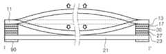
도 1은 일반적인 표시장치용 터치 패널을 도시한 사시도이고, 도 2는 도 1의 Ⅰ-Ⅰ' 라인을 따라 절단한 표시장치용 터치 패널을 도시한 단면도이다.FIG. 1 is a perspective view illustrating a typical touch panel for a display device, and FIG. 2 is a cross-sectional view illustrating the touch panel for a display device cut along the line II ′ of FIG. 1.
도 1 및 도 2에 도시된 바와 같이, 일반적인 표시장치용 터치 패널은 표시장치의 표시면 상에 배치되어 신호입력수단으로 이용되는 것으로 표시장치의 영상표시 영역과 대응되는 표시 영역(10)과, 상기 표시 영역(10)의 가장자리에 위치하는 비표시 영역(50)으로 구분된다.As shown in FIGS. 1 and 2, a touch panel for a general display device is disposed on a display surface of the display device and used as a signal input means, and includes a
일반적인 표시장치의 터치 패널은 PET 등과 같이 유연성을 가지는 투명한 상부 기판(11) 및 하부 기판(21)이 일정한 간격을 두고 배치된다.In a touch panel of a general display device, a transparent
표시 영역(10)에 있어서, 상기 상부 기판(11)의 내부 면에는 제1 투명 도전층(미도시)이 형성되고, 상기 하부 기판(21)의 내부 면에는 제2 투명 도전층(미도시)이 형성된다.In the
상기 비표시 영역(50)에 있어서, 상기 상부 기판(10)의 내부 면에는 상부전극(13)이 형성되고, 상기 하부 기판(21)의 내부 면에는 하부전극(23)이 형성된다.In the
상기 상부전극(13)은 상기 제1 투명 도전층과 전기적으로 연결되며, 상기 하부전극(23)은 상기 제2 투명 도전층과 전기적으로 연결된다.The
상기 상부 기판(11) 및 하부 기판(21)은 접착층(30)에 의해 서로 합착되며, 상기 상부 전극(13) 및 하부 전극(23)과 접착층(DAT: double adhesive tape, 30) 사이에는 제1 및 제2 절연층(17, 27)이 형성된다.The
또한, 하부 기판(21)의 하부면 가장자리에는 양면 테이프(90)가 구비되며, 터치 패널은 상기 양면 테이프(90)에 의해 표시장치상에 고정된다.In addition, a double-
그러나, 이와 같은 구조의 일반적인 표시장치용 터치 패널은 상부 기판(11)과 하부 기판(21)을 합착이 상기 접착층(30)에 의해 이루어짐으로써, 상기 접착층(30)의 접착력 약화에 의해 화살표(→) 방향으로 상부 기판(11)의 들뜸 또는 처짐이 발생하는 문제가 있었다. 상기 접착층(30)의 접착력 약화로 인한 상부 기판(11)의 들뜸 또는 처짐은 터치 신뢰도를 저하시키는 원인이 되어 터치 패널을 포함하는 표시장치의 불량을 야기하는 문제가 있었다.However, in the general touch panel for a display device having such a structure, the
본 발명은 불량률을 줄일 수 있는 구조를 가지는 표시장치용 터치 패널을 제공함에 그 목적이 있다.It is an object of the present invention to provide a touch panel for a display device having a structure capable of reducing a defective rate.
본 발명의 일 실시예에 따른 표시장치용 터치 패널은,A touch panel for a display device according to an embodiment of the present invention,
서로 일정한 간격을 두고 서로 대면되는 상부 기판 및 하부 기판; 상기 상부 기판 및 하부 기판의 서로 대면되는 면에 각각 형성된 제1 및 제2 투명 도전층; 상기 상부 기판의 가장자리에 형성되며, 상기 하부 기판과 대면되는 면에 형성된 상부 전극; 상기 하부 기판의 가장자리에 형성되며, 상기 상부 기판과 대면되는 면에 형성되는 하부 전극; 및 상기 상부 기판의 측면으로부터 연장되어 상기 하부 기판을 감싸는 벤딩부를 포함하는 것을 특징으로 한다.An upper substrate and a lower substrate facing each other at regular intervals from each other; First and second transparent conductive layers respectively formed on surfaces of the upper substrate and the lower substrate facing each other; An upper electrode formed at an edge of the upper substrate and formed on a surface facing the lower substrate; A lower electrode formed on an edge of the lower substrate and formed on a surface facing the upper substrate; And a bending part extending from a side of the upper substrate to surround the lower substrate.
이상에서 설명한 본 발명의 일 실시예에 따른 표시장치용 터치 패널은 상부 기판의 측면으로 연장된 벤딩부가 구비되어 터치 패널의 가장자리를 상기 벤딩부가 구부러져 감싸는 구조로써, 하부 기판의 하부면까지 구부러지는 벤딩부와 하부 기판의 하부면에 형성된 제2 접착층이 부착되어 상부 기판과 하부 기판의 합착 신뢰도를 향상시킬 수 있다.The touch panel for a display device according to the exemplary embodiment of the present invention described above has a bending portion extending to the side of the upper substrate to wrap the edge of the touch panel by bending the bending portion, and to bend to the lower surface of the lower substrate. The second adhesive layer formed on the lower surface of the lower and lower substrates may be attached to improve the bonding reliability of the upper and lower substrates.
즉, 본 발명의 표시장치용 터치 패널은 하부 기판의 하부면까지 구부러지는 벤딩부가 상부 기판의 측면으로 연장됨으로써, 일반적인 터치 패널에서 접착층의 접착력 약화로 인해 상부 기판의 처짐 또는 들뜸 등의 문제를 방지할 수 있다.That is, in the touch panel for the display device of the present invention, the bending portion that is bent to the lower surface of the lower substrate extends to the side of the upper substrate, thereby preventing problems such as sagging or lifting of the upper substrate due to weakened adhesive strength of the adhesive layer in the general touch panel. can do.
또한, 본 발명은 터치 패널의 상부 기판과 하부 기판의 합착 신뢰도를 향상시킴으로써, 불량률을 줄여 표시장치의 생산 수율이 향상될 수 있다.In addition, the present invention can improve the bonding reliability of the upper substrate and the lower substrate of the touch panel, thereby reducing the defective rate can be improved production yield of the display device.
첨부한 도면을 참조하여 본 발명에 따른 실시 예를 상세히 설명하도록 한다.Hereinafter, exemplary embodiments of the present invention will be described in detail with reference to the accompanying drawings.
도 3은 본 발명의 일 실시예에 따른 표시장치를 도시한 분해 사시도이고, 도 4는 도 3의 상부 기판의 하부면을 도시한 평면도이고, 도 5는 도 3의 Ⅱ-Ⅱ' 라인을 따라 절단한 표시장치용 터치 패널을 도시한 단면도이다.3 is an exploded perspective view illustrating a display device according to an exemplary embodiment of the present invention, FIG. 4 is a plan view illustrating a bottom surface of the upper substrate of FIG. 3, and FIG. 5 is along a line II-II ′ of FIG. 3. It is sectional drawing which shows the cutout touchscreen for display devices.
도 3 및 도 4에 도시된 바와 같이, 본 발명의 일 실시예에 따른 터치 패널(100)은 표시장치의 표시면 상에 배치되는 것으로 도면에서는 도시되지 않았지만, 터치 패널(100)의 하부면에는 표시장치가 배치된다.As shown in FIGS. 3 and 4, the
표시장치용 터치 패널(100)은 PET 등과 같이 유연성을 가지는 투명한 상부 기판(111) 및 하부 기판(121)을 구비하며, 상기 상부 기판(111)과 하부 기판(121)의 일정한 간격을 유지하기 위한 도트 스페이서(dot spacer, 140)가 상기 상부 기판(111)과 하부 기판(121) 사이에 형성된다. 또한, 상기 상부 기판(111)과 하부 기판(121)의 사이에는 상기 상부 기판(111) 및 하부 기판(121)을 합착시키는 제1 접착층(130a)이 형성된다. 상기 제1 접착층(130a)은 상부 기판(111)과 하부 기판(121)의 가장자리에 형성된다.The
표시장치용 터치 패널(100)의 표시 영역(a1)에 있어서, 도면에는 도시되지 않았지만, 상기 하부 기판(121)과 마주보는 상부 기판(111)의 하부면에는 제1 투명 도전층(미도시)이 형성되고, 상기 제1 투명 도전층과 대응되는 상기 하부 기판(121)의 상부면에는 제2 투명 도전층이 형성된다. 여기서, 상기 제1 및 제2 투명 도전층은 ITO(Indium-Tin-Oxide), IZO(Indium-Zinc-Oxide) 및 ITZO(Indium-Tin-Zinc-Oxide) 중 어느 하나가 이용된다.In the display area a1 of the
표시장치용 터치 패널(100)의 가장자리와 대응되는 영역은 비표시 영역(a2)으로 정의되며, 상기 비표시 영역(a2)의 상부 기판(111)에는 측면으로 돌출되어 하부 기판(121)의 가장자리를 감싸는 벤딩부(160)가 구비된다.An area corresponding to an edge of the
상기 벤딩부(160)는 상부 기판(111)의 4개의 측면으로부터 연장되며, 벤딩부(160)의 하부면에는 벤딩부(160)의 길이방향으로 제1 투명 도전층이 식각된 도전층 식각영역(161)이 위치한다.The
도전층 식각영역(161)은 벤딩부(160)가 하부 기판(121)의 측면과 하부면으로 구부러지는 경우, 제1 투명 도전층의 크랙 발생을 방지하는 역할을 한다.The conductive
도 4 및 도 5를 참조하면, 본 발명의 터치 패널(100)은 비표시 영역(a2)에 있어서, 상부 기판(111)의 하부면 가장자리에 상부 전극(113)이 형성되고, 상부 전극(113)의 하부면에 제1 절연층(117)이 형성된다.4 and 5, in the
상기 비표시 영역(a2)의 하부 기판(121) 상에는 하부 전극(123)과 제2 절연층(127)이 차례로 형성된다.The
상부 기판(111)과 하부 기판(121)은 제1 접착층(130a)에 의해 합착되며, 상기 제1 접착층(130a)은 상기 제1 및 제2 절연층(117, 127) 사이에 위치한다.The
하부 기판(121)의 하부면 가장자리에는 제2 접착층(130b)이 형성된다.The second
여기서, 상기 제1 및 제2 접착층(130a, 130b)은 접착 테이프 형태로 부착될 수 있고, 접착물질이 도포될 수도 있다.Here, the first and second
상부 기판(111)의 벤딩부(160)는 상기 상부 전극(113), 하부 전극(123), 제1 및 제2 절연층(117, 127), 제1 및 제2 접착층(130a, 130b)의 측면을 감싸며, 제2 접착층(130b) 상에 부착된다.The
상부 기판(111)과 하부 기판(121)은 제1 접착층(130a)에 의해 1차 합착되고, 상기 벤딩부(160)와 제2 접착층(130b)이 부착되어 2차 합착된다.The
상기 벤딩부(160)의 하부면에는 표시 장치와의 합착을 위한 양면 테이프(190)가 부착된다.The double-
이와 같은 구조의 표시장치의 터치 패널(100)은 측면에 구비된 연성회로기판(180)에 의해 외부로부터의 구동신호가 상부 전극(113) 및 하부 전극(123)에 공급되어 구동된다.In the
이상에서 설명한 본 발명의 일 실시예에 따른 표시장치용 터치 패널(100)은 상부 기판(111)의 측면으로 연장된 벤딩부(160)가 구비되어 터치 패널(100)의 가장자리를 상기 벤딩부(160)가 구부러져 감싸는 구조로써, 하부 기판(121)의 하부면까지 구부러지는 벤딩부(160)와 하부 기판(121)의 하부면에 형성된 제2 접착층(130b)이 부착되어 상부 기판(111)과 하부 기판(121)의 합착 신뢰도를 향상시킬 수 있다.The
즉, 본 발명의 표시장치용 터치 패널(100)은 하부 기판(121)의 하부면까지 구부러지는 벤딩부(160)가 상부 기판(111)의 측면으로 연장됨으로써, 일반적인 터치 패널에서 접착층의 접착력 약화로 인해 상부 기판(111)의 처짐 또는 들뜸 등의 문제를 방지할 수 있다.That is, in the display
또한, 본 발명은 이상에서와 같이, 터치 패널(100)의 상부 기판(111)과 하부 기판(121)의 합착 신뢰도를 향상시킴으로써, 불량률을 줄여 표시장치의 생산 수율이 향상될 수 있다.In addition, the present invention, as described above, by improving the bonding reliability of the
도 6은 본 발명의 다른 실시예에 따른 표시장치용 터치 패널의 상부 기판의 하부면을 도시한 평면도이고, 도 7은 본 발명의 또 다른 실시예에 따른 표시장치용 터치 패널을 도시한 단면도이다.6 is a plan view illustrating a bottom surface of an upper substrate of a touch panel for a display device according to another embodiment of the present invention, and FIG. 7 is a cross-sectional view illustrating a touch panel for a display device according to another embodiment of the present invention. .
도 6에 도시된 바와 같이, 본 발명의 다른 실시예에 따른 표시장치용 터치 패널은 상부 기판의 측면으로 연장된 벤딩부(260)를 포함한다.As shown in FIG. 6, the touch panel for a display device according to another exemplary embodiment of the present invention includes a
상기 벤딩부(260)의 하부면에는 벤딩부(260)가 구부러지는 경우, 상부 기판에 형성된 투명 도전층의 크랙 발생을 방지하기 위해 벤딩부(260)의 길이방향으로 투명 도전층이 식각된 도전층 식각영역(261)이 형성된다.When the
벤딩부(260)의 양 끝단의 구조는 상부 기판의 측면으로 갈수록 좁아지는 형태로 이루어진다. 보다 구체적으로 벤딩부(260)의 양 끝단은 벤딩부(260)가 구부러지는 경우, 서로 간섭하지 못하도록 경사진 구조로 이루어진다.Both ends of the bending
도 7에 도시된 바와 같이, 본 발명의 또 다른 실시예에 따른 표시장치용 터치 패널은 상부 기판(211)의 측면으로부터 연장된 벤딩부(260)를 포함한다.As shown in FIG. 7, the touch panel for a display device according to another exemplary embodiment of the present invention includes a bending
터치 패널은 상부 기판(211)과 하부 기판(221)이 합착된 구조로 이루어진다.The touch panel has a structure in which the
하부 기판(221)과 대면하는 상부 기판(211)의 하부면에는 상부 전극(213) 및 제1 절연층(217)이 차례로 형성된다.The
상부 기판(211)과 대면하는 하부 기판(221) 상에는 하부 전극(223) 및 제2 절연층(227)이 차례로 형성된다.The
하부 기판(221)의 가장자리와, 하부 전극(223) 및 제2 절연막(227)의 측면에는 접착층(230)이 형성된다.An
상기 접착층(230)은 상기 제2 졀연막(227) 상에 형성되며, 상부 기판(211)과 하부 기판(223)을 합착시키는 역할을 한다.The
상기 상부 기판(211)의 벤딩부(260)는 상부 전극(213) 및 제1 절연층(217)의 측면을 감싸고, 상기 접착층(230)을 감싸는 구조로 이루어진다.The bending
즉, 상기 벤딩부(260)는 하부 기판(221)의 하부면에 형성된 접착층(230)을 덮는 구조로 이루어진다.That is, the bending
상기 하부 기판(223)의 하부면과 대응되는 벤딩부(260)의 하부면에는 표시장치와의 합착을 위한 양면 테이프(290)가 부착된다.The double-
이상에서와 같이, 본 발명의 다른 실시예 및 또 다른 실시예에 따른 표시장치용 터치 패널은 상부 기판(211)의 측면으로 연장된 벤딩부(260)가 구비되어 터치 패널의 가장자리를 상기 벤딩부(260)가 구부러져 감싸는 구조로써, 하부 기판(221)의 하부면까지 구부러지는 벤딩부(260)와 하부 기판(221)의 하부면에 형성된 접착층(230)이 부착되어 상부 기판(211)과 하부 기판(221)의 합착 신뢰도를 향상시킬 수 있다.As described above, the touch panel for a display device according to another embodiment and another embodiment of the present invention is provided with a bending
즉, 본 발명의 표시장치용 터치 패널은 하부 기판(221)의 하부면까지 구부러지는 벤딩부(260)가 상부 기판(211)의 측면으로 연장됨으로써, 일반적인 터치 패널 에서 접착층의 접착력 약화로 인해 상부 기판(211)의 처짐 또는 들뜸 등의 문제를 방지할 수 있다.That is, in the touch panel for the display device of the present invention, the bending
또한, 본 발명은 이상에서와 같이, 터치 패널의 상부 기판(211)과 하부 기판(221)의 합착 신뢰도를 향상시킴으로써, 불량률을 줄여 표시장치의 생산 수율이 향상될 수 있다.In addition, as described above, as described above, the bonding reliability of the
이상 설명한 내용을 통해 당업자라면 본 발명의 기술사상을 일탈하지 아니하는 범위에서 다양한 변경 및 수정이 가능함을 알 수 있을 것이다. 따라서 본 발명의 기술적 범위는 명세서의 상세한 설명에 기재된 내용으로 한정되는 것이 아니라 특허 청구의 범위에 의해 정하여져야만 할 것이다.Those skilled in the art will appreciate that various changes and modifications can be made without departing from the technical spirit of the present invention. Therefore, the technical scope of the present invention should not be limited to the contents described in the detailed description of the specification but should be defined by the claims.
도 1은 일반적인 표시장치용 터치 패널을 도시한 사시도이다.1 is a perspective view illustrating a general touch panel for a display device.
도 2는 도 1의 Ⅰ-Ⅰ' 라인을 따라 절단한 표시장치용 터치 패널을 도시한 단면도이다.FIG. 2 is a cross-sectional view illustrating a touch panel for a display device cut along the line II ′ of FIG. 1.
도 3은 본 발명의 일 실시예에 따른 표시장치를 도시한 분해 사시도이다.3 is an exploded perspective view illustrating a display device according to an exemplary embodiment of the present invention.
도 4는 도 3의 상부 기판의 하부면을 도시한 평면도이다.4 is a plan view illustrating a bottom surface of the upper substrate of FIG. 3.
도 5는 도 3의 Ⅱ-Ⅱ' 라인을 따라 절단한 표시장치용 터치 패널을 도시한 단면도이다.FIG. 5 is a cross-sectional view illustrating a touch panel for a display device cut along a line II-II ′ of FIG. 3.
도 6은 본 발명의 다른 실시예에 따른 표시장치용 터치 패널의 상부 기판의 하부면을 도시한 평면도이다.6 is a plan view illustrating a bottom surface of an upper substrate of a touch panel for a display device according to another exemplary embodiment of the present invention.
도 7은 본 발명의 또 다른 실시예에 따른 표시장치용 터치 패널을 도시한 단면도이다.7 is a cross-sectional view illustrating a touch panel for a display device according to another exemplary embodiment of the present invention.
Claims (7)
Translated fromKoreanPriority Applications (1)
| Application Number | Priority Date | Filing Date | Title |
|---|---|---|---|
| KR1020080081454AKR101510888B1 (en) | 2008-08-20 | 2008-08-20 | Touch panel for display device |
Applications Claiming Priority (1)
| Application Number | Priority Date | Filing Date | Title |
|---|---|---|---|
| KR1020080081454AKR101510888B1 (en) | 2008-08-20 | 2008-08-20 | Touch panel for display device |
Publications (2)
| Publication Number | Publication Date |
|---|---|
| KR20100022780Atrue KR20100022780A (en) | 2010-03-03 |
| KR101510888B1 KR101510888B1 (en) | 2015-04-10 |
Family
ID=42175213
Family Applications (1)
| Application Number | Title | Priority Date | Filing Date |
|---|---|---|---|
| KR1020080081454AExpired - Fee RelatedKR101510888B1 (en) | 2008-08-20 | 2008-08-20 | Touch panel for display device |
Country Status (1)
| Country | Link |
|---|---|
| KR (1) | KR101510888B1 (en) |
Cited By (4)
| Publication number | Priority date | Publication date | Assignee | Title |
|---|---|---|---|---|
| KR20160114799A (en)* | 2015-03-24 | 2016-10-06 | 삼성디스플레이 주식회사 | Display apparatus |
| KR20170080735A (en)* | 2015-12-30 | 2017-07-11 | 삼성디스플레이 주식회사 | Flexible display apparatus |
| KR101866329B1 (en)* | 2017-02-28 | 2018-06-11 | (주)엔피홀딩스 | Preventing the front plate protrusion ir touch screen |
| US10026379B2 (en) | 2015-10-01 | 2018-07-17 | Samsung Display Co., Ltd. | Display device |
Family Cites Families (2)
| Publication number | Priority date | Publication date | Assignee | Title |
|---|---|---|---|---|
| KR100822187B1 (en)* | 2001-10-18 | 2008-04-16 | 삼성에스디아이 주식회사 | Touch panel and flat panel display device using same |
| KR20070068576A (en)* | 2005-12-27 | 2007-07-02 | 주식회사 테라디스플레이 | Structure to improve touch panel performance |
- 2008
- 2008-08-20KRKR1020080081454Apatent/KR101510888B1/ennot_activeExpired - Fee Related
Cited By (4)
| Publication number | Priority date | Publication date | Assignee | Title |
|---|---|---|---|---|
| KR20160114799A (en)* | 2015-03-24 | 2016-10-06 | 삼성디스플레이 주식회사 | Display apparatus |
| US10026379B2 (en) | 2015-10-01 | 2018-07-17 | Samsung Display Co., Ltd. | Display device |
| KR20170080735A (en)* | 2015-12-30 | 2017-07-11 | 삼성디스플레이 주식회사 | Flexible display apparatus |
| KR101866329B1 (en)* | 2017-02-28 | 2018-06-11 | (주)엔피홀딩스 | Preventing the front plate protrusion ir touch screen |
Also Published As
| Publication number | Publication date |
|---|---|
| KR101510888B1 (en) | 2015-04-10 |
Similar Documents
| Publication | Publication Date | Title |
|---|---|---|
| US10310673B2 (en) | Electrostatic capacitance-type input device and input device-attached electro-optical apparatus | |
| US9778805B2 (en) | Electrostatic capacitance input device and electro-optical device having input device | |
| CN104346011B (en) | Display device with touch-screen | |
| US11119616B2 (en) | Trace transfer techniques for touch sensor panels with flex circuits | |
| EP2746907B1 (en) | Touch display device and method of manufacturing the same | |
| CN102109939B (en) | Capacitive input device and there is the electro-optic device of input function | |
| CN111354765B (en) | Flexible display device | |
| KR102053258B1 (en) | Touch window | |
| TWI508106B (en) | Touch panel and handheld electronic device | |
| TWI386711B (en) | Flat display device unified with touch panel | |
| CN105739799B (en) | Electrostatic capacitive type touch screen panel | |
| CN103823599A (en) | Electrostatic capacitive type touch screen panel | |
| US20110315536A1 (en) | Touch panel | |
| CN102385462A (en) | Type touch screen panel | |
| CN102722300B (en) | Touch panel and touch display panel | |
| JP2014081910A (en) | Touch panel and manufacturing method of the same | |
| US8681091B2 (en) | Bistable display device | |
| TWI630517B (en) | Touch window and touch device including the same | |
| KR101510888B1 (en) | Touch panel for display device | |
| KR102262553B1 (en) | Touch panel | |
| KR102095240B1 (en) | Touch sensor integrated type display device with narrow bezel area | |
| US11385737B1 (en) | Electronic device | |
| CN111290655A (en) | Display device and electronic apparatus | |
| KR101450901B1 (en) | touch panel for display device | |
| KR100469357B1 (en) | Touch panel |
Legal Events
| Date | Code | Title | Description |
|---|---|---|---|
| PA0109 | Patent application | St.27 status event code:A-0-1-A10-A12-nap-PA0109 | |
| PG1501 | Laying open of application | St.27 status event code:A-1-1-Q10-Q12-nap-PG1501 | |
| R18-X000 | Changes to party contact information recorded | St.27 status event code:A-3-3-R10-R18-oth-X000 | |
| R18-X000 | Changes to party contact information recorded | St.27 status event code:A-3-3-R10-R18-oth-X000 | |
| R18-X000 | Changes to party contact information recorded | St.27 status event code:A-3-3-R10-R18-oth-X000 | |
| R17-X000 | Change to representative recorded | St.27 status event code:A-3-3-R10-R17-oth-X000 | |
| A201 | Request for examination | ||
| PA0201 | Request for examination | St.27 status event code:A-1-2-D10-D11-exm-PA0201 | |
| D13-X000 | Search requested | St.27 status event code:A-1-2-D10-D13-srh-X000 | |
| D14-X000 | Search report completed | St.27 status event code:A-1-2-D10-D14-srh-X000 | |
| E902 | Notification of reason for refusal | ||
| PE0902 | Notice of grounds for rejection | St.27 status event code:A-1-2-D10-D21-exm-PE0902 | |
| E13-X000 | Pre-grant limitation requested | St.27 status event code:A-2-3-E10-E13-lim-X000 | |
| P11-X000 | Amendment of application requested | St.27 status event code:A-2-2-P10-P11-nap-X000 | |
| P13-X000 | Application amended | St.27 status event code:A-2-2-P10-P13-nap-X000 | |
| E701 | Decision to grant or registration of patent right | ||
| PE0701 | Decision of registration | St.27 status event code:A-1-2-D10-D22-exm-PE0701 | |
| PR0701 | Registration of establishment | St.27 status event code:A-2-4-F10-F11-exm-PR0701 | |
| PR1002 | Payment of registration fee | St.27 status event code:A-2-2-U10-U11-oth-PR1002 Fee payment year number:1 | |
| PG1601 | Publication of registration | St.27 status event code:A-4-4-Q10-Q13-nap-PG1601 | |
| PR1001 | Payment of annual fee | St.27 status event code:A-4-4-U10-U11-oth-PR1001 Fee payment year number:4 | |
| FPAY | Annual fee payment | Payment date:20190318 Year of fee payment:5 | |
| PR1001 | Payment of annual fee | St.27 status event code:A-4-4-U10-U11-oth-PR1001 Fee payment year number:5 | |
| PR1001 | Payment of annual fee | St.27 status event code:A-4-4-U10-U11-oth-PR1001 Fee payment year number:6 | |
| PR1001 | Payment of annual fee | St.27 status event code:A-4-4-U10-U11-oth-PR1001 Fee payment year number:7 | |
| PR1001 | Payment of annual fee | St.27 status event code:A-4-4-U10-U11-oth-PR1001 Fee payment year number:8 | |
| PC1903 | Unpaid annual fee | St.27 status event code:A-4-4-U10-U13-oth-PC1903 Not in force date:20230404 Payment event data comment text:Termination Category : DEFAULT_OF_REGISTRATION_FEE | |
| PC1903 | Unpaid annual fee | St.27 status event code:N-4-6-H10-H13-oth-PC1903 Ip right cessation event data comment text:Termination Category : DEFAULT_OF_REGISTRATION_FEE Not in force date:20230404 |