KR20100020771A - Method for fabricating semiconductor package - Google Patents
Method for fabricating semiconductor packageDownload PDFInfo
- Publication number
- KR20100020771A KR20100020771AKR1020080079517AKR20080079517AKR20100020771AKR 20100020771 AKR20100020771 AKR 20100020771AKR 1020080079517 AKR1020080079517 AKR 1020080079517AKR 20080079517 AKR20080079517 AKR 20080079517AKR 20100020771 AKR20100020771 AKR 20100020771A
- Authority
- KR
- South Korea
- Prior art keywords
- semiconductor
- substrate
- semiconductor chip
- wafer
- semiconductor package
- Prior art date
- Legal status (The legal status is an assumption and is not a legal conclusion. Google has not performed a legal analysis and makes no representation as to the accuracy of the status listed.)
- Withdrawn
Links
- 239000004065semiconductorSubstances0.000titleclaimsabstractdescription108
- 238000000034methodMethods0.000titleclaimsabstractdescription22
- 239000000758substrateSubstances0.000claimsabstractdescription40
- 239000000945fillerSubstances0.000claimsabstractdescription21
- 238000004519manufacturing processMethods0.000claimsabstractdescription19
- 239000002184metalSubstances0.000claimsdescription14
- 238000005452bendingMethods0.000claimsdescription11
- 239000000835fiberSubstances0.000claimsdescription5
- 239000003365glass fiberSubstances0.000claimsdescription5
- 239000000463materialSubstances0.000description6
- 238000005538encapsulationMethods0.000description4
- 230000002265preventionEffects0.000description4
- 229910000679solderInorganic materials0.000description4
- 239000007788liquidSubstances0.000description2
- 239000002390adhesive tapeSubstances0.000description1
- 230000015572biosynthetic processEffects0.000description1
- 230000003247decreasing effectEffects0.000description1
- 230000008054signal transmissionEffects0.000description1
- 230000003313weakening effectEffects0.000description1
Images


Classifications
- H—ELECTRICITY
- H01—ELECTRIC ELEMENTS
- H01L—SEMICONDUCTOR DEVICES NOT COVERED BY CLASS H10
- H01L23/00—Details of semiconductor or other solid state devices
- H01L23/28—Encapsulations, e.g. encapsulating layers, coatings, e.g. for protection
- H—ELECTRICITY
- H01—ELECTRIC ELEMENTS
- H01L—SEMICONDUCTOR DEVICES NOT COVERED BY CLASS H10
- H01L24/00—Arrangements for connecting or disconnecting semiconductor or solid-state bodies; Methods or apparatus related thereto
- H01L24/01—Means for bonding being attached to, or being formed on, the surface to be connected, e.g. chip-to-package, die-attach, "first-level" interconnects; Manufacturing methods related thereto
- H01L24/10—Bump connectors ; Manufacturing methods related thereto
- H—ELECTRICITY
- H01—ELECTRIC ELEMENTS
- H01L—SEMICONDUCTOR DEVICES NOT COVERED BY CLASS H10
- H01L24/00—Arrangements for connecting or disconnecting semiconductor or solid-state bodies; Methods or apparatus related thereto
- H01L24/01—Means for bonding being attached to, or being formed on, the surface to be connected, e.g. chip-to-package, die-attach, "first-level" interconnects; Manufacturing methods related thereto
- H01L24/26—Layer connectors, e.g. plate connectors, solder or adhesive layers; Manufacturing methods related thereto
- H—ELECTRICITY
- H01—ELECTRIC ELEMENTS
- H01L—SEMICONDUCTOR DEVICES NOT COVERED BY CLASS H10
- H01L24/00—Arrangements for connecting or disconnecting semiconductor or solid-state bodies; Methods or apparatus related thereto
- H01L24/01—Means for bonding being attached to, or being formed on, the surface to be connected, e.g. chip-to-package, die-attach, "first-level" interconnects; Manufacturing methods related thereto
- H01L24/50—Tape automated bonding [TAB] connectors, i.e. film carriers; Manufacturing methods related thereto
- H—ELECTRICITY
- H01—ELECTRIC ELEMENTS
- H01L—SEMICONDUCTOR DEVICES NOT COVERED BY CLASS H10
- H01L2224/00—Indexing scheme for arrangements for connecting or disconnecting semiconductor or solid-state bodies and methods related thereto as covered by H01L24/00
- H01L2224/01—Means for bonding being attached to, or being formed on, the surface to be connected, e.g. chip-to-package, die-attach, "first-level" interconnects; Manufacturing methods related thereto
- H01L2224/10—Bump connectors; Manufacturing methods related thereto
- H01L2224/15—Structure, shape, material or disposition of the bump connectors after the connecting process
- H01L2224/16—Structure, shape, material or disposition of the bump connectors after the connecting process of an individual bump connector
- H—ELECTRICITY
- H01—ELECTRIC ELEMENTS
- H01L—SEMICONDUCTOR DEVICES NOT COVERED BY CLASS H10
- H01L2224/00—Indexing scheme for arrangements for connecting or disconnecting semiconductor or solid-state bodies and methods related thereto as covered by H01L24/00
- H01L2224/01—Means for bonding being attached to, or being formed on, the surface to be connected, e.g. chip-to-package, die-attach, "first-level" interconnects; Manufacturing methods related thereto
- H01L2224/26—Layer connectors, e.g. plate connectors, solder or adhesive layers; Manufacturing methods related thereto
- H01L2224/27—Manufacturing methods
- H01L2224/274—Manufacturing methods by blanket deposition of the material of the layer connector
- H—ELECTRICITY
- H01—ELECTRIC ELEMENTS
- H01L—SEMICONDUCTOR DEVICES NOT COVERED BY CLASS H10
- H01L2924/00—Indexing scheme for arrangements or methods for connecting or disconnecting semiconductor or solid-state bodies as covered by H01L24/00
- H01L2924/15—Details of package parts other than the semiconductor or other solid state devices to be connected
- H01L2924/151—Die mounting substrate
- H01L2924/153—Connection portion
- H01L2924/1531—Connection portion the connection portion being formed only on the surface of the substrate opposite to the die mounting surface
- H01L2924/15311—Connection portion the connection portion being formed only on the surface of the substrate opposite to the die mounting surface being a ball array, e.g. BGA
Landscapes
- Engineering & Computer Science (AREA)
- Computer Hardware Design (AREA)
- Microelectronics & Electronic Packaging (AREA)
- Power Engineering (AREA)
- Physics & Mathematics (AREA)
- Condensed Matter Physics & Semiconductors (AREA)
- General Physics & Mathematics (AREA)
- Wire Bonding (AREA)
Abstract
Translated fromKoreanDescription
Translated fromKorean본 발명은 반도체 패키지의 제조 방법에 관한 것으로서, 보다 상세하게는, 플립 칩 타입의 반도체 패키지 제조 방법에 관한 것이다.The present invention relates to a method for manufacturing a semiconductor package, and more particularly, to a method for manufacturing a flip chip type semiconductor package.
각종 전기/전자 제품의 크기가 소형화되는 추세에 따라, 한정된 크기의 기판에 보다 많은 수의 칩을 실장시켜 소형이면서도 고용량을 달성하고자 하는 많은 연구가 전개되고 있고, 이에 따라, 기판 상에 실장되는 반도체 패키지의 크기 및 두께가 점차 감소되고 있는 실정이다.As the size of various electric / electronic products is miniaturized, many studies have been developed to achieve a small size and high capacity by mounting a larger number of chips on a limited size substrate, and thus, a semiconductor mounted on the substrate. The size and thickness of the package is gradually decreasing.
전형적인 반도체 패키지는 금속와이어를 매개로 인쇄회로 기판과 전기적으로 연결되며, 금속와이어를 이용한 전기적 연결은 공정 진행이 용이하고 신뢰성 측면에서 우수하다는 잇점이 있지만, 칩과 인쇄회로기판 사이의 전기적 신호 전달 길이가 길고 패키지의 크기가 크다는 불리함이 있다.A typical semiconductor package is electrically connected to a printed circuit board via metal wires, and the electrical connection using metal wires is easy to process and has excellent reliability, but the electrical signal transmission length between the chip and the printed circuit board is long. The disadvantage is that it is long and the size of the package is large.
이에, 전형적인 반도체 패키지의 크기 및 전기적 특성을 개선시키기 위하여 플립 칩(Flip chip) 타입의 반도체 패키지가 제안되었으며, 플립 칩 타입 반도체 패키지는 반도체 칩의 본딩 패드와 기판의 접속 패드 간에 구비된 범프(Bump)를 통해 전기적인 연결이 이루어진 구조를 갖는다.Accordingly, in order to improve the size and electrical characteristics of a typical semiconductor package, a flip chip type semiconductor package has been proposed, and a flip chip type semiconductor package includes a bump provided between a bonding pad of a semiconductor chip and a connection pad of a substrate. ) Has a structure in which electrical connection is made.
한편, 플립 칩 타입 반도체 패키지는 반도체 칩과 기판의 열팽창계수 차이로 인하여 그들과 접합된 범프의 상,하부 면에 전단 응력이 부가되어 솔더 접합 부분에 크랙(Crack)이 발생할 가능성이 크다. 또한, 범프의 높이로 인해 반도체 칩과 기판 사이에 갭(Gap)이 형성되어 반도체 칩의 지지력이 약화되는 경우가 있다.On the other hand, in the flip chip type semiconductor package, shear stress is applied to the upper and lower surfaces of the bumps bonded to them due to the difference in thermal expansion coefficients between the semiconductor chip and the substrate, and cracks are likely to occur in the solder joint. In addition, a gap may be formed between the semiconductor chip and the substrate due to the height of the bump, thereby weakening the holding force of the semiconductor chip.
이를 방지하기 위하여, 플립 칩 타입 반도체 패키지에서는 액상의 충진재 형성 물질을 주입 및 경화시키는, 소위, 언더필 공정을 수행하여 반도체 칩과 인쇄회로기판 사이에 충진재를 형성한다.In order to prevent this, in the flip chip type semiconductor package, a filling material is formed between the semiconductor chip and the printed circuit board by performing a so-called underfill process of injecting and curing a liquid filling material forming material.
그러나, 최근 반도체 패키지의 소형화를 구현하기 위하여 반도체 칩의 두께가 얇아짐에 따라 반도체 칩에 휨(Warpage)이 발생하게 되고, 상기 휨은 반도체 칩과 기판 사이에 충진재를 개재시키는, 소위, 언더필 공정 공정을 수행하기 어렵게 하는 원인이 되었다.However, in recent years, in order to realize miniaturization of a semiconductor package, as the thickness of a semiconductor chip becomes thin, warpage occurs in the semiconductor chip, and the warpage is a so-called underfill process in which a filler is interposed between the semiconductor chip and the substrate. The process was difficult to carry out.
즉, 반도체 칩의 두께가 얇아짐에 따라 범프를 매개로 기판 상에 부착된 반도체 칩의 가장자리 부분이 기판의 방향으로 휘어지게 되어 기판과 반도체 칩 사시의 간격이 좁아진다. 이에 따라, 액상의 충진재 형성 물질이 반도체 칩과 기판 사이에 주입되지 못하여 경우가 발생하게 되며, 충진재의 불완전한 충진에 의해 반도체 칩들과 기판의 사이 공간에 제품의 신뢰성을 저하시키는 보이드가 발생하게 된다.That is, as the thickness of the semiconductor chip becomes thinner, the edge portion of the semiconductor chip attached to the substrate through the bumps is bent in the direction of the substrate, so that the gap between the substrate and the semiconductor chip is narrowed. As a result, a liquid filling material forming material may not be injected between the semiconductor chip and the substrate, and incomplete filling of the filler may cause voids to reduce the reliability of the product in the space between the semiconductor chips and the substrate.
또한, 반도체 칩의 휨에 의해 범프가 반도체 칩 및 기판으로부터 분리되는 현상 등이 발생하여 전기적인 연결에 문제가 발생한다.In addition, a phenomenon in which the bump is separated from the semiconductor chip and the substrate due to the bending of the semiconductor chip occurs, thereby causing a problem in electrical connection.
본 발명은 얇은 두께를 갖는 반도체 칩의 휨을 방지하여 안정적으로 충진재 형성 공정을 수행할 수 있는 플립 칩 타입의 반도체 패키지 제조 방법을 제공한다.The present invention provides a method of manufacturing a flip chip type semiconductor package capable of stably forming a filler forming process by preventing bending of a semiconductor chip having a thin thickness.
본 발명에 따른 반도체 패키지의 제조 방법은, 상면에 다수의 본딩 패드들이 구비된 복수개의 반도체 칩들을 포함하는 웨이퍼의 상기 상면과 마주하는 하면 상에 휨 방지 부재를 부착하는 단계; 상기 웨이퍼를 다수의 반도체 칩들로 개별화하는 단계; 상기 개별화된 각 반도체 칩의 상기 본딩 패드들 및 상기 각 본딩 패드들과 대응하는 상면 부분에 형성된 기판의 접속패드들을 접속 부재들을 매개로 전기적으로 연결하는 단계; 및 상기 각 반도체 칩과 기판 사이에 충진재를 형성하는 단계를 포함한다.According to an aspect of the present invention, there is provided a method of manufacturing a semiconductor package, the method including: attaching a warpage preventing member on a lower surface of the wafer, the upper surface of the wafer including a plurality of semiconductor chips having a plurality of bonding pads; Individualizing the wafer into a plurality of semiconductor chips; Electrically connecting the bonding pads of the individual semiconductor chips and the connection pads of the substrate formed on the upper surface portions corresponding to the respective bonding pads through connection members; And forming a filler between each semiconductor chip and the substrate.
상기 웨이퍼의 하면 상에 휨 방지 부재를 부착하는 단계 전, 웨이퍼의 하면을 연마하여 상기 반도체 칩들의 두께를 줄이는 단계를 더 포함한다.The method may further include grinding the lower surface of the wafer to reduce the thickness of the semiconductor chips before attaching the warpage preventing member to the lower surface of the wafer.
상기 각 반도체 칩과 기판 사이에 충진재를 형성하는 단계 후, 상기 각 반도체 칩 하면에 부착된 휨 방지 부재를 제거하는 단계를 더 포함한다.After forming the filler between the semiconductor chip and the substrate, the method further includes the step of removing the warpage preventing member attached to the lower surface of the semiconductor chip.
상기 휨 방지 부재는 테이프로 형성한다.The said bending prevention member is formed of a tape.
상기 테이프는 내부에 유리섬유(Glass fiber)를 함유하여 형성한다.The tape is formed by containing glass fiber (Glass fiber) therein.
상기 테이프는 내부에 금속플레이트(Metal plate)를 함유하여 형성한다.The tape is formed by containing a metal plate (metal plate) therein.
상기 테이프는 내부에 금속 섬유(Metal fiber)를 함유하여 형성한다.The tape is formed by containing a metal fiber (Metal fiber) therein.
상기 접속 부재는 범프를 포함한다.The connecting member includes a bump.
본 발명은 얇은 두께를 갖는 반도체 칩의 하면에 휨 방지 부재를 형성하여 충진재 형성 공정을 수행함으로써 반도체 칩과 기판 사이에 용이하게 충진재를 형성할 수 있으며, 이에 따라, 충진재의 불완전한 형성으로 발생하는 보이드를 방지할 수 있고, 이에 따라, 신뢰성이 향상된 박형 반도체 패키지를 제조할 수 있다.According to the present invention, a filler may be easily formed between a semiconductor chip and a substrate by forming a warpage preventing member on a lower surface of a semiconductor chip having a thin thickness, thereby forming voids between the semiconductor chip and the substrate. Can be prevented, and accordingly, a thin semiconductor package with improved reliability can be manufactured.
또한, 반도체 칩의 휨이 방지되어 범프가 반도체 칩 및 기판으로부터 분리되는 현상 등을 방지할 수 있어 전기적 특성이 향상된 박형 반도체 패키지를 제조할 수 있다.In addition, the bending of the semiconductor chip is prevented to prevent the bump from being separated from the semiconductor chip and the substrate, thereby manufacturing a thin semiconductor package having improved electrical characteristics.
이하, 첨부된 도면을 참조하여 본 발명의 실시예들에 따른 반도체 패키지 및 그의 제조 방법에 대하여 상세히 설명하지만, 본 발명은 하기의 실시예들에 제한된 것은 아니며, 해당 분야에서 통상의 지식을 가진 자라면 본 발명의 기술적 사상을 벗어나지 않는 범위 내에서 본 발명에 따른 반도체 패키지를 다양한 다른 형태로 구현 할 수 있을 것이다.Hereinafter, a semiconductor package and a method of manufacturing the same according to embodiments of the present invention will be described in detail with reference to the accompanying drawings. However, the present invention is not limited to the following embodiments, and a person of ordinary skill in the art. If so, the semiconductor package according to the present invention may be implemented in various other forms without departing from the technical spirit of the present invention.
본 발명에 따른 반도체 패키지의 제조 방법은, 상면에 다수의 본딩 패드들이 구비된 복수개의 반도체 칩들을 포함하는 웨이퍼의 상기 상면과 마주하는 하면 상에 휨 방지 부재를 부착하는 단계; 상기 웨이퍼를 다수의 반도체 칩들로 개별화하는 단계; 상기 개별화된 각 반도체 칩의 상기 본딩 패드들 및 상기 각 본딩 패드들과 대응하는 상면 부분에 형성된 기판의 접속패드들을 접속 부재들을 매개로 전기적으로 연결하는 단계; 및 상기 각 반도체 칩과 기판 사이에 충진재를 형성하는 단 계를 포함한다.According to an aspect of the present invention, there is provided a method of manufacturing a semiconductor package, the method including: attaching a warpage preventing member on a lower surface of the wafer, the upper surface of the wafer including a plurality of semiconductor chips having a plurality of bonding pads; Individualizing the wafer into a plurality of semiconductor chips; Electrically connecting the bonding pads of the individual semiconductor chips and the connection pads of the substrate formed on the upper surface portions corresponding to the respective bonding pads through connection members; And forming a filler between each of the semiconductor chips and the substrate.
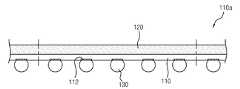
도 1a 내지 도 1d는 본 발명의 실시예에 따른 반도체 패키지의 제조 방법을 설명하기 위한 단면도이다.1A to 1D are cross-sectional views illustrating a method of manufacturing a semiconductor package in accordance with an embodiment of the present invention.
도 1a를 참조하면, 상면에 다수의 본딩 패드(112)들이 구비되고, 소자의 제조 공정이 완료된 복수개의 반도체 칩(110)들을 포함하는 웨이퍼(110a)의 상면에 백그라인딩용 테이프(미도시)를 부착한다.Referring to FIG. 1A, a plurality of
그런 다음, 웨이퍼(110a)의 상면과 마주하는 웨이퍼(110a)의 하면에 백그라인딩 공정으로 웨이퍼(110a)의 하면을 연마하여 각 반도체 칩(110)들의 두께를 줄인다.Then, the bottom surface of the
이어서, 상기 백그라인딩 테이프를 제거한다.Subsequently, the backgrinding tape is removed.
도 1b를 참조하면, 두께가 줄어든 웨이퍼(110a)의 하면 상에 웨이퍼(110a)를 칩 단위로 절단할 경우 발생하는 각 반도체 칩(110)들의 휨을 방지하기 위하여 휨 방지 부재(120)를 부착한다.Referring to FIG. 1B, a
휨 방지 부재(120)는 반도체 칩(110)의 가장자리 부분이 휘는 방향으로 작용하는 응력과 반대되는 방향으로 응력이 작용하는 특성을 갖는 고강성의 테이프를 포함하며, 바람직하게, 접착성을 갖는 테이프를 포함한다. 자세하게, 휨 방지 부재(120)는 내부에 유리섬유(Glass fiber) 및 금속섬유(Metal fiber)가 함유된 테이프로 형성하거나 반도체 칩(110)에서 발생하는 열을 외부로 신속하게 방출시키기 위하여 내부에 금속플레이트(Metal plate)를 함유하는 테이프로 형성한다.The
그런 다음, 반도체 칩(110)들의 상면에 구비된 각 본딩 패드(112)들 상에 전 기적인 연결을 위한 접속 부재(130)를 형성한다. 접속 부재(130)는 공지된 다양한 종류의 전기적 연결 구성물을 포함하며, 바람직하게, 범프로 형성한다.Then, the
도 1c를 참조하면, 상기 웨이퍼를 절단하여 상기 웨이퍼를 다수의 반도체 칩(110)들로 개별화한다. 휨 방지 부재(120)는 상기 웨이퍼의 절단시, 반도체 칩(110)들과 함께 절단되어 각 반도체 칩(110)의 하면에 배치된다.Referring to FIG. 1C, the wafer is cut to individualize the wafer into a plurality of
이후, 개별화된 각 반도체 칩(110)들을 상면에 각 반도체 칩(110)의 각 본딩 패드(112)들과 대응하는 부분에 접속 패드(142)들이 형성된 기판(140)의 상면 상에 접속 부재(130)을 매개로 부착하여 반도체 칩(110)과 기판(140)을 전기적으로 연결시킨다.Subsequently, the individualized
반도체 칩(110)과 기판(140)의 연결은 접속 부재(130)를 기판(140)의 접속 패드(142) 상에 형성한 후, 기판(140)의 상면 상에 상면에 다수의 본딩 패드(112)들이 구비되고 하면에 휨 방지 부재(130)가 부착된 반도체 칩(110)을 부착하는 방법으로 수행할 수 있다.The connection between the
도 1d를 참조하면, 접속 부재(130)를 매개로 연결된 반도체 칩(110)과 기판(130)의 사이 공간에 충진재(150)를 형성시킨다. 충진재(150)는 반도체 칩(110)과 기판(140)의 열팽창 계수 차이로 인하여 접속 부재(130)의 상,하부 면에 전단 응력이 부가되어 발생하는 솔더 접합 부분의 크랙과 같은 변형을 방지하기 위하여 형성한다. 충진재(150)는 공지된 바와 같이, 충진재 형성 물질을 주입 및 경화시키는 방법으로 형성하며, 휨 방지 부재(120)에 의해 반도체 칩(110)의 휨이 방지됨에 따라 충진재(150) 형성 공정은 용이하게 수행될 수 있다.Referring to FIG. 1D, a
그런 다음, 반도체 칩(110) 하면의 상기 휨 방지 부재를 제거한다.Then, the warpage prevention member on the bottom surface of the
이어서, 상기 기판(140)의 상면 상에 반도체 칩(110)을 덮는 봉지부(160)를 형성하고, 기판(140)의 하면에 솔더볼과 같은 외부접속단자를 부착하여 본 발명에 따른 플립 칩 타입의 반도체 패키지(100) 제조를 완료한다.Subsequently, an
한편, 도 2는 본 발명의 다른 실시예에 따른 반도체 패키지의 제조 방법을 설명하기 위한 단면도이다.2 is a cross-sectional view illustrating a method of manufacturing a semiconductor package according to another embodiment of the present invention.
도 2는 앞서 도 1a 내지 도 1d에 도시 및 설명된 반도체 패키지와 실질적으로 동일한 구성 요소를 포함한다. 따라서, 동일한 구성 요소에 대한 중복된 설명은 생략하기로 하며, 동일한 구성 요소에 대해서는 동일한 명칭 및 동일한 참조 부호를 부여하기로 한다.FIG. 2 includes substantially the same components as the semiconductor package shown and described above with reference to FIGS. 1A-1D. Therefore, duplicate descriptions of the same components will be omitted, and the same components and the same reference numerals will be given to the same components.
도 2를 참조하면, 상기 도 1d에 도시된 바와 같이 충진재(150)를 형성한 후, 기판(140)의 상면 상에 하면에 휨 방지 부재(120)가 부착된 반도체 칩(110)을 덮도록 봉지부(160)를 형성한다. 이때, 휨 방지 부재(120)는, 바람직하게, 반도체 칩(110)에서 발생하는 열을 신속하게 외부로 방출시키기 위하여 내부에 금속 플레이트가 함유된 테이프로 이루어진다.Referring to FIG. 2, after the
그런 다음, 상기 기판(140)의 상면 상에 반도체 칩(110)의 측면을 덮는 봉지부(160)를 형성하고, 기판(140)의 하면에 솔더볼과 같은 외부접속단자를 부착하여 본 발명에 따른 플립 칩 타입의 반도체 패키지(100) 제조를 완료한다.Then, an
아울러, 반도체 칩(110)의 하면으로 봉지부(160)가 형성되지 않는 반도체 패키지의 경우, 휨 방지 부재(120)로 금속 플레이트가 함유된 테이프를 사용하는 것 이 바람직하다.In addition, in the case of the semiconductor package in which the
이상에서와 같이, 본 발명은 얇은 두께를 갖는 반도체 칩을 이용하여 플립 칩 타입의 박형 반도체 패키지를 형성하는 경우, 얇은 두께의 반도체 칩에 의해 반도체 칩과 기판 사이에 충진재가 불완전하게 형성되는 것을 방지하기 위하여 반도체 칩의 하면에 휨 방지 부재를 형성한 후, 충진재 형성 공정을 수행한다.As described above, when the flip chip type thin semiconductor package is formed by using a semiconductor chip having a thin thickness, the filler is prevented from being incompletely formed between the semiconductor chip and the substrate by the thin semiconductor chip. In order to form a bending prevention member on the lower surface of the semiconductor chip, a filler forming step is performed.
따라서, 상기 휨 방지 부재에 의해 반도체 칩의 휨이 방지되어 반도체 칩과 기판 사이에 용이하게 충진재를 형성할 수 있음에 따라, 충진재의 불완전한 형성으로 발생하는 보이드를 방지할 수 있고, 이에 따라, 신뢰성이 향상된 박형 반도체 패키지를 제조할 수 있다.Therefore, since the warpage of the semiconductor chip is prevented by the warpage preventing member, the filler can be easily formed between the semiconductor chip and the substrate, thereby preventing voids caused by incomplete formation of the filler, and thus, reliability. This improved thin semiconductor package can be manufactured.
또한, 반도체 칩의 휨이 방지되어 범프가 반도체 칩 및 기판으로부터 분리되는 현상 등을 방지할 수 있어 전기적 특성이 향상된 박형 반도체 패키지를 제조할 수 있다.In addition, the bending of the semiconductor chip is prevented to prevent the bump from being separated from the semiconductor chip and the substrate, thereby manufacturing a thin semiconductor package having improved electrical characteristics.
이상, 여기에서는 본 발명을 특정 실시예에 관련하여 도시하고 설명하였지만, 본 발명이 그에 한정되는 것은 아니며, 이하의 특허청구의 범위는 본 발명의 정신과 분야를 이탈하지 않는 한도 내에서 본 발명이 다양하게 개조 및 변형될 수 있다는 것을 당업계에서 통상의 지식을 가진 자가 용이하게 알 수 있다.As mentioned above, although the present invention has been illustrated and described with reference to specific embodiments, the present invention is not limited thereto, and the following claims are not limited to the scope of the present invention without departing from the spirit and scope of the present invention. It can be easily understood by those skilled in the art that can be modified and modified.
도 1a 내지 도 1d는 본 발명의 실시예에 따른 반도체 패키지의 제조 방법을 설명하기 위한 단면도.1A to 1D are cross-sectional views illustrating a method of manufacturing a semiconductor package in accordance with an embodiment of the present invention.
도 2는 본 발명의 다른 실시예에 따른 반도체 패키지의 제조 방법을 설명하기 위한 단면도.2 is a cross-sectional view illustrating a method of manufacturing a semiconductor package in accordance with another embodiment of the present invention.
Claims (8)
Translated fromKoreanPriority Applications (1)
| Application Number | Priority Date | Filing Date | Title |
|---|---|---|---|
| KR1020080079517AKR20100020771A (en) | 2008-08-13 | 2008-08-13 | Method for fabricating semiconductor package |
Applications Claiming Priority (1)
| Application Number | Priority Date | Filing Date | Title |
|---|---|---|---|
| KR1020080079517AKR20100020771A (en) | 2008-08-13 | 2008-08-13 | Method for fabricating semiconductor package |
Publications (1)
| Publication Number | Publication Date |
|---|---|
| KR20100020771Atrue KR20100020771A (en) | 2010-02-23 |
Family
ID=42090718
Family Applications (1)
| Application Number | Title | Priority Date | Filing Date |
|---|---|---|---|
| KR1020080079517AWithdrawnKR20100020771A (en) | 2008-08-13 | 2008-08-13 | Method for fabricating semiconductor package |
Country Status (1)
| Country | Link |
|---|---|
| KR (1) | KR20100020771A (en) |
Cited By (2)
| Publication number | Priority date | Publication date | Assignee | Title |
|---|---|---|---|---|
| KR20160078658A (en)* | 2014-12-24 | 2016-07-05 | 앰코 테크놀로지 코리아 주식회사 | Semiconductor package and manufacturing method thereof |
| KR20170029892A (en)* | 2015-09-08 | 2017-03-16 | 삼성전자주식회사 | Tube-type lens, OES(Optical Emission Spectroscopy) apparatus comprising the tube-type lens, plasma monitoring system comprising the OES apparatus, and method for fabricating semiconductor device using the system |
- 2008
- 2008-08-13KRKR1020080079517Apatent/KR20100020771A/ennot_activeWithdrawn
Cited By (2)
| Publication number | Priority date | Publication date | Assignee | Title |
|---|---|---|---|---|
| KR20160078658A (en)* | 2014-12-24 | 2016-07-05 | 앰코 테크놀로지 코리아 주식회사 | Semiconductor package and manufacturing method thereof |
| KR20170029892A (en)* | 2015-09-08 | 2017-03-16 | 삼성전자주식회사 | Tube-type lens, OES(Optical Emission Spectroscopy) apparatus comprising the tube-type lens, plasma monitoring system comprising the OES apparatus, and method for fabricating semiconductor device using the system |
Similar Documents
| Publication | Publication Date | Title |
|---|---|---|
| JP4705748B2 (en) | Manufacturing method of semiconductor device | |
| JP5543086B2 (en) | Semiconductor device and manufacturing method thereof | |
| US20100261311A1 (en) | Method of manufacturing a semiconductor device | |
| JP5104734B2 (en) | Highly reliable semiconductor device production method and system | |
| JP2002289769A (en) | Stacked semiconductor device and method of manufacturing the same | |
| CN101221946A (en) | Semiconductor package and method for manufacturing system-in-package module | |
| JP2001338947A (en) | Flip chip type semiconductor device and its manufacturing method | |
| JP2007103737A (en) | Semiconductor device | |
| KR102066015B1 (en) | Semiconductor package and method of manufacturing the same | |
| TWI741207B (en) | Semiconductor device | |
| US20110316150A1 (en) | Semiconductor package and method for manufacturing semiconductor package | |
| KR20130129100A (en) | Semiconductor device and method of manufacturing the same | |
| KR100698527B1 (en) | Chip stack package having pillar bumps using metal bumps and method for manufacturing same | |
| KR100748558B1 (en) | Chip size package and its manufacturing method | |
| JP2009049218A (en) | Semiconductor device, and manufacturing method of semiconductor device | |
| JP4899406B2 (en) | Flip chip type semiconductor device | |
| JP2006222470A (en) | Semiconductor device and manufacturing method thereof | |
| KR100674501B1 (en) | Semiconductor chip mounting method using flip chip bonding technology | |
| KR20100020771A (en) | Method for fabricating semiconductor package | |
| US8035220B2 (en) | Semiconductor packaging device | |
| TW200536074A (en) | Chip package structure and process for fabricating the same | |
| JP4620553B2 (en) | Manufacturing method of semiconductor device | |
| JP4626445B2 (en) | Manufacturing method of semiconductor package | |
| JP6792322B2 (en) | Semiconductor devices and methods for manufacturing semiconductor devices | |
| JP5078631B2 (en) | Semiconductor device |
Legal Events
| Date | Code | Title | Description |
|---|---|---|---|
| PA0109 | Patent application | Patent event code:PA01091R01D Comment text:Patent Application Patent event date:20080813 | |
| PG1501 | Laying open of application | ||
| PC1203 | Withdrawal of no request for examination | ||
| WITN | Application deemed withdrawn, e.g. because no request for examination was filed or no examination fee was paid |