KR20090130089A - Diodes and Active Matrix Displays - Google Patents
Diodes and Active Matrix DisplaysDownload PDFInfo
- Publication number
- KR20090130089A KR20090130089AKR1020097022582AKR20097022582AKR20090130089AKR 20090130089 AKR20090130089 AKR 20090130089AKR 1020097022582 AKR1020097022582 AKR 1020097022582AKR 20097022582 AKR20097022582 AKR 20097022582AKR 20090130089 AKR20090130089 AKR 20090130089A
- Authority
- KR
- South Korea
- Prior art keywords
- film
- electrode
- semiconductor film
- substrate
- gate
- Prior art date
- Legal status (The legal status is an assumption and is not a legal conclusion. Google has not performed a legal analysis and makes no representation as to the accuracy of the status listed.)
- Ceased
Links
Images


Classifications
- H—ELECTRICITY
- H10—SEMICONDUCTOR DEVICES; ELECTRIC SOLID-STATE DEVICES NOT OTHERWISE PROVIDED FOR
- H10D—INORGANIC ELECTRIC SEMICONDUCTOR DEVICES
- H10D30/00—Field-effect transistors [FET]
- H10D30/60—Insulated-gate field-effect transistors [IGFET]
- H10D30/67—Thin-film transistors [TFT]
- H10D30/6729—Thin-film transistors [TFT] characterised by the electrodes
- H—ELECTRICITY
- H10—SEMICONDUCTOR DEVICES; ELECTRIC SOLID-STATE DEVICES NOT OTHERWISE PROVIDED FOR
- H10D—INORGANIC ELECTRIC SEMICONDUCTOR DEVICES
- H10D30/00—Field-effect transistors [FET]
- H10D30/60—Insulated-gate field-effect transistors [IGFET]
- H10D30/67—Thin-film transistors [TFT]
- H10D30/6704—Thin-film transistors [TFT] having supplementary regions or layers in the thin films or in the insulated bulk substrates for controlling properties of the device
- H10D30/6713—Thin-film transistors [TFT] having supplementary regions or layers in the thin films or in the insulated bulk substrates for controlling properties of the device characterised by the properties of the source or drain regions, e.g. compositions or sectional shapes
- H10D30/6715—Thin-film transistors [TFT] having supplementary regions or layers in the thin films or in the insulated bulk substrates for controlling properties of the device characterised by the properties of the source or drain regions, e.g. compositions or sectional shapes characterised by the doping profiles, e.g. having lightly-doped source or drain extensions
- H—ELECTRICITY
- H10—SEMICONDUCTOR DEVICES; ELECTRIC SOLID-STATE DEVICES NOT OTHERWISE PROVIDED FOR
- H10D—INORGANIC ELECTRIC SEMICONDUCTOR DEVICES
- H10D30/00—Field-effect transistors [FET]
- H10D30/60—Insulated-gate field-effect transistors [IGFET]
- H10D30/67—Thin-film transistors [TFT]
- H10D30/6729—Thin-film transistors [TFT] characterised by the electrodes
- H10D30/6737—Thin-film transistors [TFT] characterised by the electrodes characterised by the electrode materials
- H10D30/6739—Conductor-insulator-semiconductor electrodes
- H—ELECTRICITY
- H10—SEMICONDUCTOR DEVICES; ELECTRIC SOLID-STATE DEVICES NOT OTHERWISE PROVIDED FOR
- H10D—INORGANIC ELECTRIC SEMICONDUCTOR DEVICES
- H10D30/00—Field-effect transistors [FET]
- H10D30/60—Insulated-gate field-effect transistors [IGFET]
- H10D30/67—Thin-film transistors [TFT]
- H10D30/674—Thin-film transistors [TFT] characterised by the active materials
- H10D30/6755—Oxide semiconductors, e.g. zinc oxide, copper aluminium oxide or cadmium stannate
- H—ELECTRICITY
- H10—SEMICONDUCTOR DEVICES; ELECTRIC SOLID-STATE DEVICES NOT OTHERWISE PROVIDED FOR
- H10D—INORGANIC ELECTRIC SEMICONDUCTOR DEVICES
- H10D30/00—Field-effect transistors [FET]
- H10D30/60—Insulated-gate field-effect transistors [IGFET]
- H10D30/67—Thin-film transistors [TFT]
- H10D30/6757—Thin-film transistors [TFT] characterised by the structure of the channel, e.g. transverse or longitudinal shape or doping profile
- H—ELECTRICITY
- H10—SEMICONDUCTOR DEVICES; ELECTRIC SOLID-STATE DEVICES NOT OTHERWISE PROVIDED FOR
- H10D—INORGANIC ELECTRIC SEMICONDUCTOR DEVICES
- H10D64/00—Electrodes of devices having potential barriers
- H10D64/20—Electrodes characterised by their shapes, relative sizes or dispositions
- H10D64/27—Electrodes not carrying the current to be rectified, amplified, oscillated or switched, e.g. gates
- H10D64/311—Gate electrodes for field-effect devices
- H10D64/411—Gate electrodes for field-effect devices for FETs
- H10D64/511—Gate electrodes for field-effect devices for FETs for IGFETs
- H—ELECTRICITY
- H10—SEMICONDUCTOR DEVICES; ELECTRIC SOLID-STATE DEVICES NOT OTHERWISE PROVIDED FOR
- H10D—INORGANIC ELECTRIC SEMICONDUCTOR DEVICES
- H10D64/00—Electrodes of devices having potential barriers
- H10D64/60—Electrodes characterised by their materials
- H10D64/62—Electrodes ohmically coupled to a semiconductor
- H—ELECTRICITY
- H10—SEMICONDUCTOR DEVICES; ELECTRIC SOLID-STATE DEVICES NOT OTHERWISE PROVIDED FOR
- H10D—INORGANIC ELECTRIC SEMICONDUCTOR DEVICES
- H10D8/00—Diodes
- H—ELECTRICITY
- H10—SEMICONDUCTOR DEVICES; ELECTRIC SOLID-STATE DEVICES NOT OTHERWISE PROVIDED FOR
- H10D—INORGANIC ELECTRIC SEMICONDUCTOR DEVICES
- H10D86/00—Integrated devices formed in or on insulating or conducting substrates, e.g. formed in silicon-on-insulator [SOI] substrates or on stainless steel or glass substrates
- H10D86/40—Integrated devices formed in or on insulating or conducting substrates, e.g. formed in silicon-on-insulator [SOI] substrates or on stainless steel or glass substrates characterised by multiple TFTs
- H10D86/421—Integrated devices formed in or on insulating or conducting substrates, e.g. formed in silicon-on-insulator [SOI] substrates or on stainless steel or glass substrates characterised by multiple TFTs having a particular composition, shape or crystalline structure of the active layer
- H10D86/423—Integrated devices formed in or on insulating or conducting substrates, e.g. formed in silicon-on-insulator [SOI] substrates or on stainless steel or glass substrates characterised by multiple TFTs having a particular composition, shape or crystalline structure of the active layer comprising semiconductor materials not belonging to the Group IV, e.g. InGaZnO
- H—ELECTRICITY
- H10—SEMICONDUCTOR DEVICES; ELECTRIC SOLID-STATE DEVICES NOT OTHERWISE PROVIDED FOR
- H10D—INORGANIC ELECTRIC SEMICONDUCTOR DEVICES
- H10D86/00—Integrated devices formed in or on insulating or conducting substrates, e.g. formed in silicon-on-insulator [SOI] substrates or on stainless steel or glass substrates
- H10D86/40—Integrated devices formed in or on insulating or conducting substrates, e.g. formed in silicon-on-insulator [SOI] substrates or on stainless steel or glass substrates characterised by multiple TFTs
- H10D86/481—Integrated devices formed in or on insulating or conducting substrates, e.g. formed in silicon-on-insulator [SOI] substrates or on stainless steel or glass substrates characterised by multiple TFTs integrated with passive devices, e.g. auxiliary capacitors
- H—ELECTRICITY
- H10—SEMICONDUCTOR DEVICES; ELECTRIC SOLID-STATE DEVICES NOT OTHERWISE PROVIDED FOR
- H10D—INORGANIC ELECTRIC SEMICONDUCTOR DEVICES
- H10D86/00—Integrated devices formed in or on insulating or conducting substrates, e.g. formed in silicon-on-insulator [SOI] substrates or on stainless steel or glass substrates
- H10D86/40—Integrated devices formed in or on insulating or conducting substrates, e.g. formed in silicon-on-insulator [SOI] substrates or on stainless steel or glass substrates characterised by multiple TFTs
- H10D86/60—Integrated devices formed in or on insulating or conducting substrates, e.g. formed in silicon-on-insulator [SOI] substrates or on stainless steel or glass substrates characterised by multiple TFTs wherein the TFTs are in active matrices
Landscapes
- Thin Film Transistor (AREA)
- Liquid Crystal (AREA)
- Electroluminescent Light Sources (AREA)
- Devices For Indicating Variable Information By Combining Individual Elements (AREA)
- Electrodes Of Semiconductors (AREA)
- Metal-Oxide And Bipolar Metal-Oxide Semiconductor Integrated Circuits (AREA)
- Formation Of Insulating Films (AREA)
Abstract
Translated fromKoreanDescription
Translated fromKorean본 발명은, 다이오드 및 액티브 매트릭스 표시장치에 관한 것이다.The present invention relates to a diode and an active matrix display.
액정 표시장치나 EL(Electroluminescence; 전계발광) 표시장치의 표시 패널에 사용되는 반도체장치, 예를 들어, TFT(Thin Film Transistor; 박막트랜지스터)의 반도체 부분은, 통상, a-Si(아모르퍼스 실리콘)나 poly-Si(다결정 실리콘)를 사용하여 형성되어 있다.A semiconductor device used for a display panel of a liquid crystal display device or an EL (Electroluminescence) display device, for example, a semiconductor portion of a thin film transistor (TFT) is usually a-Si (amorphous silicon). Or poly-Si (polycrystalline silicon).
Si(규소)는 큰 밴드 갭(band gap)을 가지지 않고(예를 들어, 단결정 Si의 밴드 갭은 1.1 eV이다), 가시광을 흡수한다. 이 광의 조사에 의해, Si 내에 전자와 정공(캐리어)이 형성된다. TFT의 채널 형성 영역에 Si막을 사용하면, 오프(OFF) 상태에서도 광의 조사에 의해 채널 형성 영역에서 캐리어가 생성되어, 소스 영역과 드레인 영역 사이에서 전류가 흐른다. 오프 상태일 때 흐르는 전류는 "오프 리크(OFF-leak) 전류"라 불리고, 이 값이 크면, 표시 패널이 정상적으로 동작하지 않 는다. 따라서, Si막에 광이 조사되지 않도록 차광막을 형성하고 있다. 그러나, 차광막을 형성하기 위해서는, 퇴적 공정, 포토리소그래피 공정, 에칭 공정이 필요하게 되기 때문에, 공정이 번잡하게 된다.Si (silicon) does not have a large band gap (for example, the band gap of single crystal Si is 1.1 eV) and absorbs visible light. By irradiation of this light, electrons and holes (carriers) are formed in Si. When the Si film is used in the channel formation region of the TFT, carriers are generated in the channel formation region by irradiation of light even in the OFF state, and a current flows between the source region and the drain region. The current flowing in the off state is called "off-leak current", and when this value is large, the display panel does not operate normally. Therefore, the light shielding film is formed so that light may not be irradiated to Si film. However, in order to form a light shielding film, since a deposition process, a photolithography process, and an etching process are needed, a process becomes complicated.
이와 같은 문제를 해결하기 위해, Si의 밴드 갭보다 큰 3.4 eV의 밴드 갭을 가지는 반도체인 산화아연(ZnO)을 사용한 투명 트랜지스터가 주목받고 있다. 이와 같은 투명 트랜지스터에서는, 밴드 갭이 가시광 대역의 광 에너지보다 크고, 가시광이 흡수되지 않는다. 따라서, 광이 조사되어도 오프 리크 전류가 증대하지 않는다는 이점(利點)을 가진다.In order to solve this problem, a transparent transistor using zinc oxide (ZnO), which is a semiconductor having a bandgap of 3.4 eV larger than the bandgap of Si, has attracted attention. In such a transparent transistor, the band gap is larger than the light energy of the visible light band and no visible light is absorbed. Therefore, there is an advantage that the off-leak current does not increase even when light is irradiated.
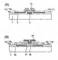
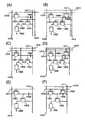
채널 형성 영역에 ZnO를 사용한 반도체장치가, 예를 들어, 문헌 1에 개시되어 있다. ZnO를 사용한 반도체장치의 구성을 도 7(A)를 참조하여 설명한다.A semiconductor device using ZnO in the channel formation region is disclosed, for example, in
도 7(A)의 반도체장치는, 유리 기판 등의 절연성 기판(1000) 위에 제공된 소스 전극(1001) 및 드레인 전극(1002), 그 소스 전극(1001) 및 드레인 전극(1002)에 접하도록 배치된 ZnO층(1003), 그 ZnO층(1003) 위에 적층된 게이트 절연층(1004), 및 게이트 전극(1005)을 가지고 있다.The semiconductor device in FIG. 7A is disposed to be in contact with a
소스 전극(1001) 및 드레인 전극(1002)에는, III족 원소인 B(붕소), Al(알루미늄), Ga(갈륨), In(인듐), Tl(탈륨); VII족 원소인 F(불소), Cl(염소), Br(브롬), I(요오드)); I족 원소인 Li(리튬), Na(나트륨), K(칼륨), Rb(루비듐), Cs(세슘)); V족 원소인 N(질소), P(인), As(비소), Sb(안티몬), Bi(비스무트)) 중의 어느 하나를 도핑한 도전성 ZnO가 사용되고 있다.The
[문헌 1] 일본국 공개특허공고 2000-150900호 공보[Document 1] Japanese Unexamined Patent Publication No. 2000-150900
본 발명자의 검토에 따르면, 도 7(A)에 나타낸 탑 게이트형 반도체장치의 소스 전극(1001) 및 드레인 전극(1002)을 형성할 때의 에칭에 의해 기판(1000)이 에칭되는 경우가 있는 것을 알 수 있었다. 기판(1000) 위에 산화규소막이나 산화질화규소막으로 형성된 하지막(1006)을 형성한 경우에도, 이 하지막이 에칭되어 기판(1000)의 표면이 노출되는 경우가 있는 것을 알 수 있었다. 또한, 도 7(B)에 나타낸 보텀 게이트형 반도체장치의 경우에는, 소스 전극(1001) 및 드레인 전극(1002)을 형성할 때의 에칭에 의해, 산화규소막이나 산화질화규소막으로 형성된 게이트 절연막(1004)이 에칭되는 것을 알 수 있었다.According to the examination of the present inventors, the
탑 게이트형 반도체장치의 경우, 유리 기판(1000)이나, 산화규소막 또는 산화질화규소막으로 형성된 하지막(1006)이 에칭되면, 기판(1000)으로부터 나트륨 등의 불순물이 반도체막(1003)내로 확산하여, 특성을 열화(劣化)시킨다.In the case of the top gate semiconductor device, when the
보텀 게이트형 반도체장치(도 7(B))의 경우에는, 소스 전극(1001) 및 드레인 전극(1002)의 형성 시의 에칭에 의해 게이트 절연막(1004)이 에칭되면, 특성이 안정하지 않고, 불량의 원인이 된다.In the case of a bottom gate type semiconductor device (FIG. 7B), when the
본 발명은 상기 사정을 감안하여 이루어진 것으로, 그의 목적은, 채널 형성 영역에 ZnO 반도체막을 사용하고, n형 또는 p형 불순물을 첨가한 ZnO막을 소 스 전극 및 드레인 전극에 사용했을 때에도, 결함이나 불량이 생기지 않는 반도체장치 및 그의 제조방법을 제공하는데 있다.SUMMARY OF THE INVENTION The present invention has been made in view of the above circumstances, and an object thereof is a defect or defect even when a ZnO semiconductor film is used in a channel formation region and a ZnO film to which n-type or p-type impurities are added to a source electrode and a drain electrode. This invention provides a semiconductor device that does not occur and a method of manufacturing the same.
본 발명의 반도체장치의 일 양태는, 산화규소막 또는 산화질화규소막 위의 Al막 또는 Al 합금막과, 그 Al막 또는 Al 합금막 위의 n형 또는 p형 불순물이 첨가된 ZnO막을 가진다. 본 명세서에서의 "산화규소막", "산화질화규소막", "Al막", "Al 합금막", "ZnO막"은 각각 산화규소를 함유하는 막, 산화질화규소를 함유하는 막, Al을 함유하는 막, Al 합금을 함유하는 막, ZnO를 함유하는 막을 의미하는 것으로 한다.One aspect of the semiconductor device of the present invention includes an Al film or an Al alloy film on a silicon oxide film or a silicon oxynitride film, and a ZnO film to which n-type or p-type impurities are added on the Al film or Al alloy film. The "silicon oxide film", "silicon oxynitride film", "Al film", "Al alloy film", and "ZnO film" in the present specification each contain a silicon oxide film, a silicon oxynitride film, and Al. It means a film, a film containing Al alloy, and a film containing ZnO.
본 발명의 반도체장치의 일 양태는, 게이트 전극 위의 산화규소막 또는 산화질화규소막으로 형성된 게이트 절연막과, 그 게이트 절연막 위의 Al막 또는 Al 합금막과, 그 Al막 또는 Al 합금막 위의 n형 또는 p형 불순물이 첨가된 ZnO막과, n형 또는 p형 불순물이 첨가된 ZnO막 위와 게이트 절연막 위의 ZnO 반도체막을 가진다.One aspect of the semiconductor device of the present invention is a gate insulating film formed of a silicon oxide film or a silicon oxynitride film on a gate electrode, an Al film or Al alloy film on the gate insulating film, and n on the Al film or Al alloy film. A ZnO film to which a type or p type impurity is added, and a ZnO semiconductor film on a ZnO film to which an n type or p type impurity is added and a gate insulating film.
본 발명의 반도체장치의 일 양태는, 산화규소막 또는 산화질화규소막 위의 Al막 또는 Al 합금막과, 그 Al막 또는 Al 합금막 위의 n형 또는 p형 불순물이 첨가된 ZnO막과, 상기 산화규소막 또는 산화질화규소막 위 및 n형 또는 p형 불순물이 첨가된 ZnO막 위의 ZnO 반도체막과, 그 ZnO 반도체막 위의 게이트 절연막과, 그 게이트 절연막 위의 게이트 전극을 가진다.One aspect of the semiconductor device of the present invention is an Al film or Al alloy film on a silicon oxide film or silicon oxynitride film, a ZnO film to which n-type or p-type impurities are added on the Al film or Al alloy film, and A ZnO semiconductor film on a silicon oxide film or a silicon oxynitride film and on a ZnO film to which n-type or p-type impurities are added, a gate insulating film on the ZnO semiconductor film, and a gate electrode on the gate insulating film.
본 발명의 반도체장치 제조방법의 일 양태는, 산화규소막 또는 산화질화규소막을 형성하는 공정, 상기 산화규소막 또는 산화질화규소막 위에 Al막 또는 Al 합금막을 형성하는 공정, 상기 Al막 또는 Al 합금막 위에 n형 또는 p형 불순물이 첨 가된 ZnO막을 형성하는 공정을 포함하고, 상기 n형 또는 p형의 불순물 첨가된 ZnO막이 제1 에칭에 의해 섬 형상으로 에칭되고, 상기 Al막 또는 Al 합금막이 제2 에칭에 의해 섬 형상으로 에칭된다.One aspect of the semiconductor device manufacturing method of the present invention is a step of forming a silicon oxide film or a silicon oxynitride film, a step of forming an Al film or an Al alloy film on the silicon oxide film or silicon oxynitride film, on the Al film or Al alloy film forming a ZnO film containing n-type or p-type impurity, wherein the n-type or p-type impurity-added ZnO film is etched into an island shape by a first etching, and the Al film or Al alloy film is formed 2 is etched into an island shape by etching.
본 발명의 반도체장치 제조방법의 일 양태에서는, 상기 제2 에칭 후에, 상기 n형 또는 p형 불순물이 첨가된 ZnO막 및 상기 산화규소막 또는 산화질화규소막 위에 ZnO 반도체막이 형성된다.In one aspect of the semiconductor device manufacturing method of the present invention, after the second etching, a ZnO semiconductor film is formed on the ZnO film to which the n-type or p-type impurity is added and on the silicon oxide film or silicon oxynitride film.
보텀 게이트형의 반도체장치의 경우에는, 게이트 전극을 형성한 후에, 상기 게이트 전극 위에 상기 산화규소막 또는 산화질화규소막으로 형성된 게이트 절연막이 형성된다.In the case of a bottom gate type semiconductor device, after forming a gate electrode, a gate insulating film formed of the silicon oxide film or silicon oxynitride film is formed on the gate electrode.
탑 게이트형의 반도체장치의 경우에는, 상기 ZnO 반도체막을 형성한 후에, 게이트 절연막이 형성되고, 게이트 전극이 형성된다.In the case of the top gate semiconductor device, after forming the ZnO semiconductor film, a gate insulating film is formed, and a gate electrode is formed.
본 발명에서의 제1 에칭은 습식 에칭이어도 좋다.The first etching in the present invention may be wet etching.
본 발명에서의 제1 에칭은 버퍼드(buffered) 불산을 사용한 습식 에칭이어도 좋다.The first etching in the present invention may be a wet etching using buffered hydrofluoric acid.
본 발명에서의 제1 에칭은 건식 에칭이어도 좋다.Dry etching may be sufficient as the 1st etching in this invention.
본 발명에서의 제1 에칭은 CH4(메탄) 가스를 사용한 건식 에칭이어도 좋다.The first etching in the present invention may be a dry etching using CH4 (methane) gas.
본 발명에서의 제2 에칭은 습식 에칭이어도 좋다.The second etching in the present invention may be wet etching.
본 발명에서의 제2 에칭은 포토레지스트용의 현상액을 사용한 습식 에칭이어도 좋다.The second etching in the present invention may be wet etching using a developer for photoresist.
본 발명에서의 제2 에칭은 유기 알칼리계 수용액을 사용한 습식 에칭이어도 좋다.The second etching in the present invention may be wet etching using an organic alkali aqueous solution.
본 발명에서의 제2 에칭은 TMAH(tetramethylammonium hydroxide)를 사용한 습식 에칭이어도 좋다.The second etching in the present invention may be wet etching using TMAH (tetramethylammonium hydroxide).
또한, 본 발명의 반도체장치의 일 양태는, 게이트 전극, 그 게이트 전극 위의 게이트 절연막, 그 게이트 절연막 위의 금속 재료를 포함하는 제1 막, 그 제1 막 위의 n형 또는 p형 불순물이 첨가된 투명 반도체 재료를 포함하는 제2 막, 및 그 제2 막 위와 상기 게이트 절연막 위의 투명 반도체를 포함하는 제3 막을 가진다.One aspect of the semiconductor device of the present invention is a first film comprising a gate electrode, a gate insulating film on the gate electrode, a metal material on the gate insulating film, and an n-type or p-type impurity on the first film. And a second film comprising the added transparent semiconductor material, and a third film including the transparent semiconductor over the second film and over the gate insulating film.
또한, 본 발명의 반도체장치의 일 양태는, 기판 위의 절연막, 그 절연막 위의 금속 재료를 포함하는 제1 막, 그 제1 막 위의 n형 또는 p형 불순물이 첨가된 투명 반도체 재료를 포함하는 제2 막, 상기 절연막 위와 상기 제2 막 위의 투명 반도체 재료를 포함하는 제3 막, 그 제3 막 위의 게이트 절연막, 및 그 게이트 절연막 위의 게이트 전극을 가진다.One aspect of the semiconductor device of the present invention also includes an insulating film on a substrate, a first film containing a metal material on the insulating film, and a transparent semiconductor material to which n-type or p-type impurities are added on the first film. And a third film comprising a transparent semiconductor material on the insulating film and on the second film, a gate insulating film on the third film, and a gate electrode on the gate insulating film.
또한, 본 발명의 반도체장치 제조방법의 일 양태는, 기판 위에 절연막을 형성하는 공정, 상기 절연막 위에 금속 재료를 포함하는 제1 막을 형성하는 공정, 상기 제1 막 위에 n형 또는 p형의 불순물 첨가된 투명 반도체 재료를 포함하는 제2 막을 형성하는 공정, 상기 제2 막을 에칭하는 공정, 상기 제1 막을 에칭하는 공정을 가진다.In addition, one aspect of the method for manufacturing a semiconductor device of the present invention includes the steps of forming an insulating film on a substrate, forming a first film containing a metal material on the insulating film, and adding an n-type or p-type impurity on the first film. And a step of forming a second film containing the transparent semiconductor material, a step of etching the second film, and a step of etching the first film.
또한, 본 발명의 반도체장치 제조방법의 일 양태는, 기판 위에 게이트 전극 을 형성하는 공정, 상기 게이트 전극 위에 게이트 절연막을 형성하는 공정, 상기 게이트 절연막 위에 금속 재료를 포함하는 제1 막을 형성하는 공정, 상기 제1 막 위에 n형 또는 p형 불순물이 첨가된 투명 반도체 재료를 포함하는 제2 막을 형성하는 공정, 상기 제2 막을 에칭하는 공정, 상기 제1 막을 에칭하는 공정을 가진다.In addition, one aspect of the method of manufacturing a semiconductor device of the present invention includes the steps of forming a gate electrode on a substrate, forming a gate insulating film on the gate electrode, forming a first film comprising a metal material on the gate insulating film, And forming a second film comprising a transparent semiconductor material to which n-type or p-type impurities are added on the first film, etching the second film, and etching the first film.
탑 게이트형 반도체장치에서는, 유리 기판이나 산화규소막 또는 산화질화규소막으로 형성된 하지막이 에칭되지 않고, 기판으로부터 나트륨 등의 불순물이 반도체막 내로 확산하여 특성을 열화시키는 일이 없다.In the top gate semiconductor device, a base film formed of a glass substrate, a silicon oxide film, or a silicon oxynitride film is not etched, and impurities such as sodium do not diffuse from the substrate into the semiconductor film, thereby deteriorating characteristics.
보텀 게이트형 반도체장치에서는, 게이트 절연막이 에칭되지 않고, 그의 특성이 불안정하게 되는 일이 없다.In the bottom gate type semiconductor device, the gate insulating film is not etched and its characteristics are not unstable.
소스 전극 및 드레인 전극의 일부에 Al을 사용하고 있으므로, 배선의 저저항화를 도모할 수 있다.Since Al is used as part of the source electrode and the drain electrode, the wiring can be reduced in resistance.
이하, 본 발명의 실시형태에 대하여 첨부 도면을 참조하여 설명한다. 본 발명은 이하의 설명에 한정되지 않고, 본 발명의 취지 및 범위로부터 벗어남이 없이 그 형태 및 상세한 사항을 다양하게 변경할 수 있다는 것은 당업자라면 용이하게 이해할 수 있을 것이다. 따라서, 본 발명은 이하의 실시형태의 기재 내용에 한정하여 해석되는 것은 아니다.EMBODIMENT OF THE INVENTION Hereinafter, embodiment of this invention is described with reference to an accompanying drawing. The present invention is not limited to the following description, and it will be readily understood by those skilled in the art that various changes in form and details may be made without departing from the spirit and scope of the present invention. Therefore, this invention is not limited to description of the following embodiment.
[실시형태 1]
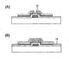
여기서는 보텀 게이트형 반도체장치에 대하여 설명한다.Here, the bottom gate semiconductor device will be described.
도 1(A)는 본 발명의 실시형태의 일례를 나타낸 단면도이다. 도 1(A)에서, 부호 1은 기판, 3은 게이트 전극, 5는 게이트 절연막, 10은 소스 전극, 10a는 제1 도전막, 10b는 제2 도전막, 11은 드레인 전극, 11a는 제1 도전막, 11b는 제2 도전막, 13은 반도체막을 나타내고 있다. 반도체막(13) 위에 패시베이션용 또는 평탄화용의 절연막을 형성하여도 좋다.1A is a cross-sectional view showing an example of an embodiment of the present invention. In Fig. 1A,
기판(1) 위에 게이트 전극(3)이 형성되고, 게이트 전극(3) 위에 게이트 절연막(5)이 형성되고, 게이트 절연막(5) 위에 소스 전극(10) 및 드레인 전극(11)이 형성되어 있다. 소스 전극(10)은 제1 도전막(10a)과 제2 도전막(10b)의 적층막으로 형성되고, 드레인 전극(11)은 제1 도전막(11a)과 제2 도전막(11b)의 적층막으로 형성되어 있다. 제1 도전막(10a)과 제2 도전막(10b) 사이, 또는 제1 도전막(11a)과 제2 도전막(11b) 사이에 제3 도전막이 형성되어 있어도 좋다. 소스 전극(10)과 드레인 전극(11)은 각각 게이트 절연막(5)을 사이에 두고 게이트 전극(3)과 일부 겹치도록 형성되어 있어도 좋다. 게이트 절연막(5) 위에서 소스 전극(10)과 드레인 전극(11) 위에 반도체막(13)이 형성되어 있다.A
이하, 각 구성에 대하여 설명한다.Hereinafter, each structure is demonstrated.
(1) 기판(1) substrate
유리 기판, 알루미나 등의 절연 물질로 형성되는 기판, 후속 공정의 처리 온도에 견딜 수 있는 플라스틱 기판 등을 사용하여 기판을 형성할 수 있다. 기판(1)에 플라스틱 기판을 사용하는 경우에는, PC(폴리카보네이트), PES(폴리에테르술폰), PET(폴리에틸렌 테레프탈레이트), PEN(폴리에틸렌 나프탈레이트) 등을 사용할 수 있다. 플라스틱 기판의 경우에는, 표면 위에 가스 배리어층으로서 무기층 또는 유기층을 제공하여도 좋다. 플라스틱 기판의 제조시의 먼지 등에 의해 기판에 돌기가 발생되어 있는 경우에는, CMP 등으로 기판을 연마하여 기판의 표면을 평탄화시킨 후에 기판을 사용하여도 좋다. 기판(1) 위에는 기판측으로부터의 불순물 등의 확산을 방지하기 위해 산화규소(SiOx), 질화규소(SiNx), 산화질화규소(SiOxNy)(x>y), 질화산화규소(SiNxOy)(x>y) 등의 절연막을 형성해 두어도 좋다.The substrate may be formed using a substrate formed of an insulating material such as a glass substrate, alumina, a plastic substrate capable of withstanding the processing temperature of a subsequent process, or the like. When using a plastic substrate for the board |
(2) 게이트 전극(2) gate electrode
Al(알루미늄)막, W(텅스텐)막, Mo(몰리브덴)막, Ta(탄탈)막, Cu(구리)막, Ti(티탄)막, 또는 상기 원소를 주성분으로 하는 합금 재료(예를 들어, Al 합금막, MoW(몰리브덴 텅스텐) 합금막) 등을 사용하여 게이트 전극을 형성할 수 있다. P(인) 등의 불순물 원소를 도핑한 다결정 규소막으로 대표되는 반도체막을 사용하여도 좋다. 또한, 게이트 전극(3)은 단층이어도 좋고, 2층 이상 적층시킨 적층막이어도 좋다.Al (aluminum) film, W (tungsten) film, Mo (molybdenum) film, Ta (tantalum) film, Cu (copper) film, Ti (titanium) film, or an alloy material containing the above elements as a main component (for example, A gate electrode can be formed using an Al alloy film, a MoW (molybdenum tungsten) alloy film), or the like. A semiconductor film represented by a polycrystalline silicon film doped with an impurity element such as P (phosphorus) may be used. The
(3) 게이트 절연막(3) gate insulating film
게이트 절연막(5)은 규소를 주성분으로 하는 절연막, 예를 들어, 산화규소막, 산화질화규소막으로 형성된다. 또한, 게이트 절연막은 단층이어도 좋고 적층막이어도 좋다.The
(4) 소스 전극 및 드레인 전극(4) source and drain electrodes
소스 전극(10)은 제1 도전막(10a)과 제2 도전막(10b)의 적층막으로 형성되고, 드레인 전극(11)은 제1 도전막(11a)과 제2 도전막(11b)의 적층막으로 형성되어 있다.The source electrode 10 is formed of a laminated film of the first
제1 도전막으로서는, Al막, AlNi(알루미늄 니켈)막이나 AlNd(알루미늄 네오디뮴)막 등의 Al 합금막을 사용할 수 있다. 제2 도전막으로서는, B(붕소), Al(알루미늄), Ga(갈륨), P(인), As(비소) 등의 p형 또는 n형 불순물이 첨가된 ZnO(산화아연)를 사용할 수 있다. 제1 도전막과 제2 도전막 사이에 제3 도전막으로서 Ti막 등의 금속막을 제공하여도 좋다.As the first conductive film, an Al alloy film such as an Al film, an AlNi (aluminum nickel) film, or an AlNd (aluminum neodymium) film can be used. As the second conductive film, ZnO (zinc oxide) to which p-type or n-type impurities such as B (boron), Al (aluminum), Ga (gallium), P (phosphorus), and As (arsenic) are added, can be used. . A metal film such as a Ti film may be provided between the first conductive film and the second conductive film as the third conductive film.
(5) 반도체막(5) semiconductor film
반도체막으로서는 ZnO막을 사용한다. 반도체막과 접하는 소스 전극 및 드레인 전극이 p형 또는 n형 불순물이 첨가된 ZnO막을 가지고 있으므로, 소스 전극 및 드레인 전극이 반도체막과 용이하게 전기적으로 접속될 수 있다.A ZnO film is used as the semiconductor film. Since the source electrode and the drain electrode in contact with the semiconductor film have a ZnO film to which p-type or n-type impurities are added, the source electrode and the drain electrode can be easily electrically connected to the semiconductor film.
(6) 절연막(6) insulating film
도시하지는 않았지만, 반도체막(13) 위에는 패시베이션막 및 평탄화막 등의 절연막을 형성하여도 좋다. 산화규소(SiOx), 질화규소(SiNx), 산화질화규소(SiOxNy)(x>y), 질화산화규소(SiNxOy)(x>y), SOG(Spin-On-Glass)막, 아크릴 등의 유기 수지막, 또는 이들의 적층막을 사용할 수 있다.Although not shown, an insulating film such as a passivation film and a planarization film may be formed on the
상기와 같은 보텀 게이트형 반도체장치에서는, 그 제조시에 게이트 절연막이 에칭되지 않고, 특성이 불안정하게 되는 일이 없다. 소스 전극 및 드레인 전극의 일부에 Al을 사용하고 있기 때문에, 배선의 저저항화를 도모할 수 있다.In the bottom gate semiconductor device as described above, the gate insulating film is not etched at the time of its manufacture, and the characteristics are not unstable. Since Al is used as part of the source electrode and the drain electrode, the wiring can be reduced in resistance.
[실시형태 2]
여기서는 탑 게이트형 반도체장치에 대하여 설명한다.Here, the top gate semiconductor device will be described.
도 1(B)는 본 발명의 실시형태의 일례를 나타낸 단면도이다. 도 1(B)에서, 부호 1은 기판, 20은 절연막, 25는 소스 전극, 25a는 제1 도전막, 25b는 제2 도전막, 26은 드레인 전극, 26a는 제1 도전막, 26b는 제2 도전막, 27은 반도체막, 28은 게이트 절연막, 29는 게이트 전극을 나타내고 있다. 게이트 전극 위에 패시베이션용 또는 평탄화용의 절연막을 형성하여도 좋다.1B is a cross-sectional view showing an example of an embodiment of the present invention. In Fig. 1B,
기판(1) 위에 절연막(20)이 형성되고, 절연막(20) 위에 소스 전극(25) 및 드레인 전극(26)이 형성되어 있다. 소스 전극(25)은 제1 도전막(25a)과 제2 도전막(25b)의 적층막으로 형성되고, 드레인 전극(26)은 제1 도전막(26a)과 제2 도전막(26b)의 적층막으로 형성되어 있다. 제1 도전막(25a)과 제2 도전막(25b) 사이, 또는 제1 도전막(26a)과 제2 도전막(26b) 사이에 제3 도전막이 형성되어 있어도 좋다. 절연막(20) 위에서 소스 전극(25) 및 드레인 전극(26) 위에 반도체막(27)이 형성되고, 반도체막(27) 위에 게이트 절연막(28)이 형성되고, 게이트 절연막(28) 위에 게이트 전극(29)이 형성되어 있다. 게이트 전극(29)은 게이트 절연막(28) 및 반도체막(27)을 사이에 두고 소스 전극(25) 및 드레인 전극(26)과 일부 겹치도록 형성되어도 좋다.An insulating
이하, 각 구성에 대하여 설명한다.Hereinafter, each structure is demonstrated.
기판, 소스 전극, 드레인 전극, 반도체막, 게이트 전극에 대해서는 실시형태 1에서 설명한 것을 사용할 수 있다.As the substrate, the source electrode, the drain electrode, the semiconductor film, and the gate electrode, those described in
(1) 기판 위의 절연막(1) insulating film on the substrate
기판(1) 위에는 기판측으로부터의 불순물 등의 확산을 방지하기 위한 절연막(20)으로서 산화규소막이나 산화질화규소막을 형성한다. 또한, 이 절연막은 단층이어도 좋고 적층막이어도 좋다.On the
(2) 게이트 절연막(2) gate insulating film
게이트 절연막(28)은 규소를 주성분으로 하는 절연막, 예를 들어, 산화규소막, 산화질화규소막, 질화산화규소막, 질화규소막으로 형성된다. 또한, 이 게이트 절연막은 단층이어도 좋고 적층막이어도 좋다.The
(3) 게이트 전극 위의 절연막(3) insulating film on the gate electrode
도시하지 않았지만, 게이트 전극(29) 위에는 패시베이션막 및 평탄화막 등의 층간절연막을 형성하여도 좋다. SiOx막, SiNx막, SiON막, SiNO막, SOG(Spin-On-Glass)막, 아크릴 등의 유기 수지막, 또는 이들의 적층막을 사용할 수 있다.Although not shown, an interlayer insulating film such as a passivation film and a planarization film may be formed on the
상기와 같은 탑 게이트형 반도체장치에서는, 그의 제조시에 기판이나 산화규소막 또는 산화질화규소막으로 형성된 하지막이 에칭되지 않으므로, 기판으로부터 나트륨 등의 불순물이 반도체막으로 확산하여 특성을 열화시키는 일이 없다. 소스 전극 및 드레인 전극의 일부에 Al을 사용하고 있기 때문에, 배선의 저저항화를 도모할 수 있다.In the top gate semiconductor device as described above, since the substrate, the silicon oxide film, or the underlying film formed of the silicon oxynitride film is not etched at the time of its manufacture, impurities such as sodium do not diffuse from the substrate into the semiconductor film to deteriorate its characteristics. . Since Al is used as part of the source electrode and the drain electrode, the wiring can be reduced in resistance.
[실시형태 3]
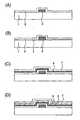
여기서는, 게이트 전극 위에 게이트 절연막으로서 산화규소막 또는 산화질화규소막을 형성하고, 제1 도전막으로서 Al막 또는 Al 합금막을 형성하고, 제2 도전막으로서 n형 또는 p형 불순물이 첨가된 ZnO막을 형성한 다음, 제2 도전막을 제1 에칭에 의해 섬 형상으로 에칭하고, 제1 도전막을 제2 에칭에 의해 섬 형상으로 에칭하여 소스 전극 및 드레인 전극을 형성하고, ZnO 반도체막을 형성하는, 보텀 게이트형 반도체장치의 제조방법에 대하여 설명한다.Here, a silicon oxide film or a silicon oxynitride film is formed on the gate electrode as a gate insulating film, an Al film or an Al alloy film is formed as a first conductive film, and a ZnO film to which n-type or p-type impurities are added is formed as a second conductive film. Next, a bottom gate type semiconductor is formed by etching the second conductive film into an island shape by a first etching, etching the first conductive film into an island shape by a second etching to form a source electrode and a drain electrode, and forming a ZnO semiconductor film. The manufacturing method of an apparatus is demonstrated.
도 2(A)에 나타내는 바와 같이, 기판(1) 위에 게이트 전극(3)을 10 nm∼200 nm의 두께로 형성한다. 기판(1)은 실시형태 1에서 나타낸 재료를 사용하여 형성할 수도 있다. 여기서는 유리 기판을 사용한다.As shown in FIG. 2A, the
기판(1) 위에는, 기판측으로부터의 불순물 등의 확산을 방지하기 위해 CVD법이나 스퍼터링법에 의해 산화규소(SiOx), 질화규소(SiNx), 산화질화규소(SiOxNy)(x>y), 질화산화규소(SiNxOy)(x>y) 등을 함유하는 절연막(2)을 10 nm∼200 nm의 두께로 형성해 두어도 좋다(도 2(B)).On the
절연막(2)은 기판(1)의 표면을 고밀도 플라즈마로 처리함으로써 형성할 수도 있다. 고밀도 플라즈마는, 예를 들어, 2.45 GHz의 마이크로파를 사용하여 생성될 수 있고, 전자 밀도가 1×10¹¹∼1×10¹³/cm3, 전자 온도가 2 eV 이하인 것만이 요구된다. 이와 같은 고밀도 플라즈마는 활성종의 운동 에너지가 낮고, 종래의 플라즈마 처리와 비교하여 플라즈마에 의한 데미지(damage)가 적고 결함이 적은 막을 형성할 수 있다.The insulating
질화성 분위기, 에를 들어, 질소와 희가스를 함유하는 분위기, 질소와 수소와 희가스를 함유하는 분위기, 또는 암모니아와 희가스를 함유하는 분위기에서의 고밀도 플라즈마 처리에 의해 기판(1)의 표면을 질화할 수 있다. 기판(1)으로서 유리 기판을 사용하고 고밀도 플라즈마에 의한 질화 처리를 행한 경우, 기판(1)의 표면 위에 형성되는 질화막으로서, 질화규소를 주성분으로 하는 절연막(2)을 형성할 수 있다. 이 질화막 위에 산화규소막 또는 산화질화규소막을 플라즈마 CVD법에 의해 형성한 다수 층을 사용하여 절연막(2)을 형성하여도 좋다.The surface of the
또한, 절연막(2)의 표면 위에, 마찬가지로 고밀도 플라즈마에 의한 질화 처리를 행함으로써, 질화막을 형성할 수 있다.In addition, a nitride film can be formed on the surface of the insulating
고밀도 플라즈마에 의한 질화 처리에 의해 형성된 질화막은 기판(1)으로부터의 불순물의 확산을 억제할 수 있다.The nitride film formed by the nitriding process by high density plasma can suppress the diffusion of impurities from the
게이트 전극(3)은 실시형태 1에서 나타낸 재료를 사용하여 형성할 수 있다. 여기서는, AlNd(알루미늄 네오디뮴)막을 AlNd 타겟을 사용하여 스퍼터링법에 의해 성막하고, 섬 형상으로 가공한다. 그 막을 섬 형상으로 가공하기 위해서는 포토리소그래피법을 이용하고, 건식 에칭이나 습식 에칭을 이용한다.The
게이트 전극(3)의 표면 및 기판(1) 또는 절연막(2)의 표면을 세정한 후, 게이트 전극(3) 위에 공지의 CVD법 또는 스퍼터링법을 이용하여 게이트 절연막(5)을 10 nm∼200 nm의 두께로 형성한다(도 2(A) 및 도 2(B)). 표면 세정 공정과 게이트 절연막(5)의 형성 공정은 대기에의 노출 없이 연속적으로 행하여도 좋다. 게이트 전극(3)에 Al막을 사용한 경우에는, 게이트 절연막(5)을 고온에서 형성하면, 힐록이 발생하는 일이 있기 때문에, 500℃ 이하, 바람직하게는 350℃ 이하의 저온에서 성막하는 것이 바람직하다.After cleaning the surface of the
게이트 절연막(5)은 실시형태 1에서 나타낸 재료를 사용하여 형성할 수 있다. 여기서는 산화규소막을 형성한다. 또한, 이하의 도면에서는 절연막(2)을 생략한다.The
게이트 절연막(5) 위에 소스 전극 및 드레인 전극용의 제1 도전막(6)을 10 nm∼200 nm의 두께로 형성한다. 제1 도전막(6)은 실시형태 1에서 나타낸 재료를 사용하여 형성할 수 있다. 여기서는 AlNi(알루미늄 니켈)막 또는 AlNd막을 사용한다. 제1 도전막(6)은 AlNi 타겟 또는 AlNd 타겟을 사용하여 스퍼터링법에 의해 형 성할 수 있다. 또한, 게이트 절연막(5)을 형성한 후, 제1 도전막(6)을 대기에의 노출 없이 연속하여 형성하여도 좋다.A first
제1 도전막(6) 위에 제2 도전막(7)을 10 nm∼200 nm의 두께로 형성한다(도 2(C)). 제2 도전막(7)은 실시형태 1에서 나타낸 재료를 사용하여 형성할 수 있다. 여기서는 Al 또는 Ga 등의 불순물이 첨가된 ZnO(산화아연)를 사용한다. 이것에 의해, 후에 반도체층으로서 형성되는 ZnO막과 제2 도전막(7)과의 사이에 오믹 콘택트(ohmic contact)가 용이하게 형성될 수 있다. 제2 도전막(7)은 스퍼터링법에 의해 형성될 수 있다. 예를 들어, Al이나 Ga을 첨가하기 위해서는, Al이나 Ga이 1∼10 중량% 첨가된 ZnO 타겟을 사용하여 스퍼터링하는 방법이나, ZnO 타겟에 Al이나 Ga의 칩(chip)을 장착하고 200∼300℃에서 스퍼터링하는 방법을 사용할 수 있다.The second
제1 도전막(6)을 형성한 후, 제2 도전막(7)을 대기에의 노출 없이 연속하여 형성하여도 좋다. 따라서, 게이트 절연막(5)으로부터 제2 도전막(7)까지의 성막은 대기에의 노출 없이 연속하여 행해질 수도 있다.After the first
제1 도전막(6)과 제2 도전막(7)과의 사이에 제3 도전막(8)을 10 nm∼200 nm의 두께로 형성하여도 좋다(도 2(D)). 제조공정에서의 열처리 온도에 따라 제1 도전막(6)과 제2 도전막(7)과의 사이의 접촉 저항이 상승하는 경우가 있다. 그러나, 제3 도전막(8)을 형성함으로써, 제1 도전막(6)과 제2 도전막(7) 사이의 접촉 저항을 낮게 할 수 있다. 제3 도전막(8)은 Ti막 등의 금속막을 사용할 수 있고, 스퍼터링법 등에 의해 형성할 수 있다.The third
제2 도전막(7) 위에 레지스트 마스크(9)를 형성하고, 제2 도전막(7)을 에칭 한다(도 3(A) 및 도 3(B)). 습식 에칭을 이용하는 경우에는, 버퍼드(buffered) 불산(HF(불화수소산)와 NH4F(불화암모늄)를 혼합한 것), 예를 들어, HF : NH4F(중량비) = 1 : 100 내지 1 : 10의 용액을 사용할 수 있다.A resist mask 9 is formed on the second
건식 에칭을 이용하는 경우에는, CH4 가스를 사용한 이방성 플라즈마 에칭을 이용할 수 있다.When dry etching is used, anisotropic plasma etching using CH4 gas can be used.
제2 도전막(7) 아래에는, 제1 도전막(6)이 형성되어 있다. 따라서, 제2 도전막(7)을 에칭할 때, 제1 도전막(6)이 에칭 스토퍼로서 작용한다. 이것에 의해, 에칭 시에 게이트 절연막(5)에 손상을 주는 일 없이 소스 전극 및 드레인 전극을 형성할 수 있다.The first
또한, 제2 도전막(7)을 에칭할 때, 제1 도전막(6)의 일부를 에칭하여도 좋다. 그러나, 제1 도전막(6)을 모두 에칭하게 되면, 게이트 절연막에 데미지를 주게 되기 때문에, 제1 도전막(6)을 모두 에칭하지 않도록 주의를 필요로 한다.In addition, when etching the 2nd
다음에, 레지스트 마스크(9)를 사용하여 제1 도전막(6)을 에칭하여 소스 전극(10) 및 드레인 전극(11)을 형성한다(도 3(C)). 본 발명에서는, 포토레지스트용 현상액인, TMAH(테트라메틸암모늄 하이드록사이드)로 대표되는 유기 알칼리계 수용액을 사용하여 제1 도전막(6)을 에칭한다.Next, the first
제1 도전막(6)에 AlNi막을 사용하고, 에칭액에 TMAH를 사용한 경우, 에칭 속도는 30℃에서 대략 300 nm/min이다. 한편, 상기한 재료를 사용한 제2 도전막(7)이나 게이트 절연막(5)은 TMAH에 의해 에칭되지 않는다. 그 결과, 게이트 절연 막(5)에 손상을 주지 않고 소스 전극(10) 및 드레인 전극(11)을 형성할 수 있다. 또한, 섬 형상의 제2 도전막(10b, 11b)은 사이즈가 축소되지 않는다. 본 발명에서는, 특수한 에칭액을 사용하지 않고 레지스트 마스크를 형성할 때의 현상액을 사용하여 제1 도전막(6)을 에칭할 수 있다. 따라서, 저비용화 및 고효율화로 이어진다.When an AlNi film is used for the first
소스 전극(10) 및 드레인 전극(11)을 형성한 후, 레지스트 마스크(9)를 제거한다.After the source electrode 10 and the
소스 전극(10), 드레인 전극(11) 및 게이트 절연막(5) 위에 반도체막(12)으로서 ZnO막을 스퍼터링법에 의해 20 nm∼200 nm의 두께로 형성한다(도 3(D)). 예를 들어, ZnO 타겟을 사용하여 산소/아르곤의 유량비를 30∼20으로 하여, 200∼300℃에서 스퍼터링함으로써 성막할 수 있다.On the source electrode 10, the
포토리소그래피법을 이용하여 반도체막(12)을 에칭하여 섬 형상의 반도체막(13)을 형성한다(도 4(A)). 에칭에는, 버퍼드 불산을 사용한 습식 에칭이나 CH4 가스를 사용한 이방성 건식 에칭을 이용할 수 있다.The
반도체막(12)과 제2 도전막(10b, 11b)에 공통으로 ZnO가 사용되고, 충분한 에칭 선택비를 얻는 것은 곤란하다. 그러나, 제2 도전막(7)은 반도체막(12)과 접하는 부분에 형성될 필요가 있기 때문에, 반도체막(12)과 접하지 않는 부분, 예를 들어, 배선 부분에서는 제2 도전막(7)이 에칭되어도 좋다. 상기한 에칭 방법에서는, 제2 도전막(10b, 11b)이 에칭될 수도 있지만, 제1 도전막(10a, 11a)은 에칭되 지 않는다. 따라서, 제1 도전막(10a, 11a)이 배선으로서 작용하고, 반도체장치와의 전기적 접속이 확보된다.ZnO is commonly used for the
반도체막(13) 위에 절연막(14)을 CVD법이나 스퍼터링법에 의해 50 nm∼1 ㎛의 두께로 형성한다(도 4(B)). 절연막(14)으로서는, 규소를 주성분으로 하는 절연막을 형성할 수 있다. 규소를 함유하는 절연막 위에 유기 수지막 등을 적층하여도 좋다. 절연막(14)은 평탄화막이나 패시베이션막으로서 기능한다. 소스 전극(10)과 드레인 전극(11)에는 Al이 포함되어 있기 때문에, 절연막(14)을 고온으로 형성하면, 힐록이 발생하는 일이 있다. 그래서, 500℃ 이하, 바람직하게는 350℃ 이하의 저온에서 형성하는 것이 바람직하다.An insulating
절연막(14)에 콘택트 홀을 형성하고, 게이트 전극(3), 소스 전극(10), 드레인 전극(11)과 접하는 도전막을 필요에 따라 제공한다.A contact hole is formed in the insulating
본 발명에 따르면, 게이트 절연막에 데미지를 주는 일 없이 반도체장치를 형성하는 것이 가능하다. 제1 도전막으로서 AlNi막 등의 Al 합금막을 사용하고 있으므로, 배선의 저저항화를 도모할 수 있다.According to the present invention, it is possible to form a semiconductor device without damaging the gate insulating film. Since Al alloy films, such as an AlNi film, are used as a 1st conductive film, wiring resistance can be reduced.
[실시형태 4]Embodiment 4
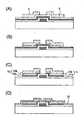
여기서는, 산화규소막 또는 산화질화규소막 위에 제1 도전막으로서 Al막 또는 Al 합금막을 형성하고, 제2 도전막으로서 n형 또는 p형 불순물이 첨가된 ZnO막을 형성한 다음, 제2 도전막을 제1 에칭에 의해 섬 형상으로 형성하고, 제1 도전막을 제2 에칭에 의해 섬 형상으로 형성하여, 소스 전극 및 드레인 전극을 형성하고, ZnO 반도체막을 형성하고, 게이트 절연막을 형성하고, 게이트 전극을 형성하는, 탑 게이트형 반도체장치의 제조방법에 대하여 설명한다. 본 실시형태에 사용하는 재료 및 제조방법은 실시형태 1∼3에서 기재한 것들을 사용할 수 있다는 것은 말할 필요도 없다.Here, an Al film or an Al alloy film is formed as a first conductive film on a silicon oxide film or a silicon oxynitride film, and a ZnO film to which n-type or p-type impurities are added as a second conductive film is formed, and then the second conductive film is formed as a first conductive film. Forming an island shape by etching, forming a first conductive film in an island shape by a second etching, forming a source electrode and a drain electrode, forming a ZnO semiconductor film, forming a gate insulating film, and forming a gate electrode. The manufacturing method of the top gate semiconductor device will be described. It goes without saying that the materials and manufacturing method used for this embodiment can use those described in Embodiments 1-3.
먼저, 도 5(A)에 나타내는 바와 같이, 기판(1) 위에 절연막(20)으로서 산화규소(SiOx)막을 CVD법이나 스퍼터링법에 의해 10 nm∼200 nm의 두께로 형성한다. 이 절연막(20)은 기판(1)측으로부터의 불순물 등의 확산을 방지한다.First, as shown in Fig. 5A, a silicon oxide (SiOx) film is formed on the
절연막(20) 위에 소스 전극 및 드레인 전극용의 제1 도전막(21)을 스퍼터링법 또는 증착법에 의해 10 nm∼200 nm의 두께로 형성한다. 제1 도전막(21)으로서는, 실시형태 1에서 나타낸 AlNi(알루미늄 니켈)막 등의 Al 합금막을 사용할 수 있다. 또한, 절연막(20)을 형성한 후, 제1 도전막(21)을 대기에의 노출 없이 연속하여 형성하여도 좋다.The first
제1 도전막(21) 위에 제2 도전막(22)을 스퍼터링법에 의해 10 nm∼200 nm의 두께로 형성한다(도 5(A)). 제2 도전막(22)으로서는, B(붕소), Al(알루미늄), Ga(갈륨), P(인), As(비소) 등의 p형 또는 n형 불순물이 첨가된 ZnO(산화아연)를 사용할 수 있다. 또한, 제1 도전막(21)을 형성한 후, 제2 도전막(22)을 대기에의 노출 없이 연속하여 형성하여도 좋다. 따라서, 절연막(20)으로부터 제2 도전막(22)까지의 형성 공정은 대기에의 노출 없이 연속하여 행해질 수도 있다.The second
제1 도전막(21)과 제2 도전막(22) 사이의 접촉 저항을 낮게 하기 위해, 제1 도전막(21)과 제2 도전막(22) 사이에 제3 도전막(23)으로서 Ti막 등의 금속막을 스 퍼터링법에 의해 10 nm∼200 nm의 두께로 형성하여도 좋다(도 5(B)).In order to lower the contact resistance between the first
제2 도전막(22) 위에 레지스트 마스크(24)를 형성하고, 제2 도전막(22)을 에칭한다(도 5(C)). 에칭 방법으로는, 버퍼드 불산을 사용한 습식 에칭 또는 CH4 가스를 사용한 건식 에칭을 사용할 수 있다.The resist
제2 도전막(22) 아래에는 제1 도전막(21)이 형성되어 있다. 따라서, 제2 도전막(22)을 에칭할 때 제1 도전막(21)이 에칭 스토퍼로서 작용한다. 이것에 의해, 절연막(20)을 에칭하여 기판(1)을 노출시키는 일 없이, 소스 전극 및 드레인 전극을 형성할 수 있다.The first
또한, 제2 도전막(22)을 에칭할 때 제1 도전막(21)의 일부를 에칭하여도 좋다. 그러나, 제1 도전막(21) 전부가 에칭되면, 절연막(20)이 에칭되고 기판(1)이 노출되어, 기판(1)에 포함되는 불순물이 확산할 가능성이 있기 때문에 주의를 필요로 한다.In addition, when etching the 2nd
제1 도전막(21)을 에칭하여 소스 전극(25) 및 드레인 전극(26)을 형성한다(도 5(D)). 에칭 방법으로는, 포토레지스트용 현상액, TMAH를 사용한 습식 에칭을 사용한다. 이것에 의해, 절연막(20)을 에칭하는 일 없이, 소스 전극(25) 및 드레인 전극(26)을 형성할 수 있다. 또한, ZnO막은 TMAH에 의해 에칭되지 않기 때문에, 섬 형상의 제2 도전막(25b, 26b)의 사이즈가 축소되는 일도 없다. 본 발명에서는, 제1 도전막(21)용으로 특수한 에칭액을 사용하지 않고 레지스트 마스크를 형성할 때의 현상액을 사용하여 에칭할 수 있어, 저비용화 및 고효율화로 이어진다.The first
소스 전극(25) 및 드레인 전극(26)을 형성한 후, 레지스트 마스크(24)를 제거한다.After the
소스 전극(25), 드레인 전극(26), 절연막(20) 위에 반도체막(27)으로서 ZnO막을 스퍼터링법에 의해 20 nm∼200 nm의 두께로 형성한다(도 6(A)).On the
반도체막(27)을 포토리소그래피법에 의해 에칭하여 섬 형상의 반도체막(27)으로 한다. 에칭 방법으로는, 버퍼드 불산을 사용한 습식 에칭이나 CH4 가스를 사용한 건식 에칭을 이용할 수 있다.The
반도체막(27)과 제2 도전막(25b, 26b)에 ZnO가 공통으로 사용되고, 높은 에칭 선택비를 얻는 것은 곤란하다. 그러나, 제2 도전막(22)은 소스 전극 및 드레인 전극부에 형성되어 있으면 좋기 때문에, 반도체막(27)과 접하지 않는 부분, 특히 배선 부분에서 제2 도전막이 에칭되어도 좋는 것은 실시형태 3과 같다.ZnO is commonly used for the
반도체막(27) 위에 게이트 절연막(28)을 CVD법이나 스퍼터링법에 의해 10 nm∼200 nm의 두께로 형성한다(도 6(B)). 반도체막(27)에 상기한 실시형태에서 기재한 고밀도 플라즈마 처리를 행하여 게이트 절연막을 형성하여도 좋다. 질화성 분위기, 예를 들어, 질소와 희가스를 함유하는 분위기, 또는 질소와 수소와 희가스를 함유하는 분위기, 또는 암모니아와 희가스를 함유하는 분위기에서 고밀도 플라즈마 처리를 행함으로써 반도체막(27)의 표면을 질화할 수 있다.The
게이트 절연막(28)은 규소를 주성분으로 하는 절연막, 예를 들어, 산화규소막, 산화질화규소막, 질화규소막, 질화산화규소막 등을 사용하여 형성하여도 좋다. 또한, 이 게이트 절연막은 단층이어도 좋고 적층막이어도 좋다.The
게이트 절연막(28) 위에 게이트 전극(29)을 형성한다(도 6(B)). 게이트 전극(29)은 상기한 실시형태에서 나타낸 재료를 사용하여 형성할 수 있고, 단층이어도 좋고 2층 이상 적층시킨 적층막이어도 좋다. 막 형성 방법으로는 공지의 CVD법, 스퍼터링법, 증착법 등을 사용할 수 있다. 또한, 포토리소그래피법으로 게이트 전극(29)을 섬 형상으로 가공하기 위해서는 건식 에칭이나 습식 에칭 방법을 이용할 수 있다.A
게이트 전극(29) 및 게이트 절연막(28) 위에 절연막(30)을 CVD법이나 스퍼터링법에 의해 50 nm∼1 ㎛의 두께로 형성한다(도 6(C)). 이 절연막(30)은 규소를 함유하는 절연막을 사용하여 형성할 수 있다. 규소를 함유하는 절연막 위에 유기 수지막 등을 적층하여도 좋다. 절연막(30)은 평탄화막이나 패시베이션막으로서 기능한다. 소스 전극(25) 및 드레인 전극(26)에는 Al이 포함되어 있기 때문에, 게이트 절연막(28), 게이트 전극(29), 절연막(30)을 고온에서 형성하면, 힐록이 발생하는 일이 있기 때문에, 500℃ 이하, 바람직하게는 350℃ 이하의 저온에서 형성하는 것이 바람직하다.On the
이와 같이, 본 발명에 따르면, 기판(1)이 노출되는 것에 의한 불순물의 확산을 방지할 수 있다. 제1 도전막으로서 AlNi막 등의 Al 합금막을 사용하고 있으므로, 배선의 저저항화를 도모할 수 있다.As described above, according to the present invention, it is possible to prevent diffusion of impurities due to the
[실시형태 5]
여기서는, 실시형태 1 및 3에서 나타낸 보텀 게이트형 반도체장치를 사용하여 액정 표시장치를 제조하는 형태에 대하여 도 8(A) 및 도 8(B)와 도 9(A) 및 도 9(B)를 사용하여 설명한다. 또한, 실시형태 2 및 4에서 나타낸 탑 게이트형 반도체장치를 적용할 수 있다는 것은 말할 필요도 없다. 도 8(A) 및 도 9(A)는 도 8(B)의 X-Y선의 단면도를 나타낸다.Here, FIGS. 8A and 8B, 9A, and 9B show a form of manufacturing a liquid crystal display device using the bottom gate semiconductor device shown in
유리 기판 또는 플라스틱 기판(1) 위에 게이트 배선(40) 및 보조 용량 배선(41)을 형성한다. 스퍼터링법으로 AlNd막을 성막하고, 그 후, 공지의 포토리소그래피법 및 에칭 방법을 이용하여 형성한다.The
산화규소막 또는 산화질소규소막으로 이루어지는 게이트 절연막(42)을 CVD법 또는 스퍼터링법으로 형성한다.A
게이트 절연막(42) 위에 제1 도전막으로서 AlNi막을 스퍼터링법으로 성막한다. 제1 도전막은 후에 소스 전극(45a), 드레인 전극(46a) 및 소스 배선(47)을 형성한다.An AlNi film is formed on the
제1 도전막 위에 제2 도전막으로서 Al이 첨가된 ZnO(산화아연)막을 스퍼터링법으로 성막한다. 제2 도전막은 후에 소스 전극(45b), 드레인 전극(46b) 및 소스 배선(47)을 형성한다.A ZnO (zinc oxide) film to which Al is added as a second conductive film is formed on the first conductive film by sputtering. The second conductive film subsequently forms a
제2 도전막 위에서, 후에 소스 전극부, 드레인 전극부, 소스 배선부가 되는 영역에 레지스트 마스크를 형성한다(도시하지 않음). 그 다음, 제2 도전막을 에칭한다. 여기서는, 버퍼드 불산과, HF : NH4F = 1 : 100(중량비)의 용액을 사용하여 에칭을 행한다.On the second conductive film, a resist mask is formed in a region which becomes a source electrode portion, a drain electrode portion, and a source wiring portion later (not shown). Next, the second conductive film is etched. Here, etching is performed using buffered hydrofluoric acid and a solution of HF: NH4 F = 1: 100 (weight ratio).
다음에, TMAH 용액을 사용하여 제1 도전막을 에칭하여 소스 전극(45a), 드레인 전극(46a), 소스 배선(47)을 형성한다. 그 후, 레지스트 마스크를 제거한다. 이것에 의해, 게이트 절연막(42)을 손상시키지 않고, 소스 전극(45), 드레인 전극(46) 및 소스 배선(47)을 형성할 수 있다. 또한, ZnO막은 TMAH에 의해 에칭되지 않기 때문에, 섬 형상의 제2 도전막의 사이즈가 축소되는 일도 없다. 또한, 제1 도전막에 AlNi막을 사용하고 있으므로, 소스 배선의 저저항화를 도모할 수 있다.Next, the first conductive film is etched using the TMAH solution to form the
다음에, 반도체막(48)을 형성한다. 스퍼터링법으로 ZnO막을 성막한 다음, 포토리소그래피법 및 에칭에 의해 ZnO막으로부터 반도체막(48)을 형성한다. 에칭에는 버퍼드 불산을 사용한 습식 에칭을 사용한다. 이때, 반도체막(48)과 접하지 않는 제2 도전막의 부분은 일부 제거되어도 좋다. 그 이유는 배선이 되는 부분에는 제1 도전막이 형성되어 있기 때문이다.Next, a
반도체막(48) 위에 절연막(49)을 CVD법, 스퍼터링법, 도포법 등에 의해 형성한다. 이 절연막(49)은 규소를 함유하는 절연막, 유기 수지막 등의 적층막을 사용하여 형성할 수 있다. 절연막(49)은 표면의 요철을 평탄화하는 막이면 좋다.The insulating
절연막(49)에 포토리소그래피법 및 에칭법을 이용하여 드레인 전극(46)에 이르는 콘택트 홀 및 보조 용량용의 콘택트 홀을 형성한다.In the insulating
투명 도전막을 스퍼터링법으로 성막한 다음, 포토리소그래피법 및 에칭 방법을 이용하여 화소 전극(50)을 형성한다. 예를 들어, ITO(Indium Tin Oxide; 인듐 주석 산화물), ITSO(산화규소를 함유하는 인듐 주석 산화물), IZO(Indium Zinc Oxide; 산화인듐 산화아연)를 사용하면 좋다.After forming a transparent conductive film by sputtering method, the
반사형 액정 표시장치의 경우에는, 투명 전극 대신에, Ag(은), Au(금), Cu(구리), W(텅스텐), Al(알루미늄) 등의 광 반사성을 가지는 금속 재료를 형성한다.In the case of the reflective liquid crystal display, instead of the transparent electrode, a metal material having light reflectivity such as Ag (silver), Au (gold), Cu (copper), W (tungsten), Al (aluminum) or the like is formed.
화소 전극(50)과 보조 용량 배선(41)이 겹치는 부분은, 화소 전극(50), 게이트 절연막(42) 및 보조 용량 배선(41)으로 형성되는 보조 용량(100)을 형성한다(도 8(A) 및 도 8(B)).The portion where the
배선 및 전극에서, 굴곡부나 폭이 변화하는 부위의 모서리를 매끈하고 둥그스름하게 하여도 좋다. 포토마스크의 패턴을 사용하여 제조되는 포토마스크 패턴을 사용하여, 모서리를 모따기한(chamfered) 형상으로 할 수 있다. 이것에 의해 이하의 효과가 있다. 플라즈마를 사용한 건식 에칭을 행할 때, 볼록부를 모따기함으로써, 이상(異常) 방전에 의한 미분(微粉)의 발생을 억제할 수 있다. 또한, 미분이 발생한 경우에도, 오목부를 모따기함으로써, 세정 시에 이 미분이 구석에 모이는 것을 방지하고 이 미분을 씻어낼 수 있다. 이렇게 하여, 제조공정에서의 먼지나 미분의 문제를 해소하여, 수율을 향상시킬 수 있다.In the wiring and the electrode, the corners of the bent portion or the portion where the width is changed may be smooth and rounded. The photomask pattern manufactured using the pattern of a photomask can be used and it can be made into the shape chamfered. This has the following effects. When performing dry etching using plasma, generation of fine powder due to abnormal discharge can be suppressed by chamfering the convex portions. Moreover, even when a fine powder generate | occur | produces, by chamfering, it can prevent this powder from gathering in a corner at the time of washing | cleaning, and can wash this fine powder. In this way, the problem of dust and fine powder in a manufacturing process can be eliminated and a yield can be improved.
그리고, 화소 전극(50)을 덮도록 배향막(51)을 형성한다. 배향막은 액적 토출법이나 인쇄법 등에 의해 형성한다. 배향막을 형성한 후, 러빙(rubbing) 처리를 행한다.The
대향 기판(56) 위에는, 착색층 및 차광층(블랙 매트릭스)을 사용하여 컬러 필터(55)를 형성하고, 보호 절연막(54)을 형성한다. 보호 절연막(54) 위에, 투명 전극(57)을 형성하고, 배향막(53)을 형성한다(도 9(A)). 배향막에는 러빙 처리를 행한다.On the
다음에, 시일재의 폐(閉)패턴(closed pattern)(75)을 액적 토출법에 의해 형성한다(도 9(B)). 이 시일재로 둘러싸인 영역에 액정 조성물(52)이 충전된다(도 9(A)).Next, a
이 폐패턴(75) 내에 액정 조성물(52)을 적하하고 나서, 대향 기판(56)과 반도체장치가 형성된 기판(1)을 서로 부착시킨다. 액정 조성물(52)을 충전하기 위해서는, 개구부를 가지는 시일(seal) 패턴을 기판(1)상에 제공하고, 대향 기판(56)과 기판(1)을 서로 부착한 다음, 모세관 현상을 이용하여 액정을 주입하여도 좋다.The
액정 조성물(52)의 배향 모드로서는, 액정 분자의 배열이 광 입사측으로부터 광 사출측을 향하여 90° 트위스트된 TN 모드, FLC 모드, IPS 모드, VA 모드 등을 사용할 수 있다. IPS 모드의 경우에는, 전극 패턴이 도 8(B)에 나타낸 것과 달리, 빗살 형상이 된다.As an orientation mode of the
반도체장치가 형성되어 있는 기판(1)과 대향 기판(56) 모두에 편광판을 부착한다. 또한, 필요에 따라, 광학 필름을 부착할 수 있다.The polarizing plate is attached to both the
반도체장치가 형성되어 있는 기판(1)과 대향 기판(56)과의 간격이, 구 형상의 스페이서를 산포하거나, 수지로 된 기둥 형상의 스페이서를 형성하거나, 시일재에 필러를 혼합시키는 것에 의해 유지되어도 좋다. 상기 기둥 형상의 스페이서는, 아크릴, 폴리이미드, 폴리이미드아미드, 에폭시 중의 적어도 하나를 주성분으로 하는 유기 수지 재료, 또는 산화규소, 질화규소, 질소를 함유하는 산화규소 중의 어 느 1종의 재료, 또는 이들의 적층막으로 이루어지는 무기 재료로 형성된다.The space | interval of the board |
그 다음, 이방성 도전체층을 사이에 끼우고 기판(1)에 공지의 기술을 사용하여 FPC(Flexible Printed Circuit)를 부착한다.Then, an anisotropic conductor layer is sandwiched between and a flexible printed circuit (FPC) is attached to the
주변 구동회로를 기판 위에 형성하여도 좋다. 평면 모식도를 도 9(B)에 나타낸다.Peripheral drive circuits may be formed on the substrate. A plan schematic diagram is shown in FIG. 9 (B).
유리 등으로 형성된 기판(61) 위에, 게이트 배선 구동회로(62), 소스 배선 구동회로(63), 액티브 매트릭스부(64)가 형성되어 있다. 게이트 배선 구동회로(62)는 적어도 시프트 레지스터(62a)와 버퍼(62b)로 구성된다. 소스 배선 구동회로(63)는 적어도 시프트 레지스터(63a)와, 버퍼(63b)와, 비디오 라인(68)을 통하여 보내지는 비디오 신호를 샘플링하는 아날로그 스위치(69)로 구성된다. 액티브 매트릭스부(64)에는, 게이트 배선 구동회로(62)로부터 연장하는 다수의 게이트 배선(72)이 평행하게 배치되어 있다. 소스 배선 구동회로(63)로부터 연장하는 다수의 소스 배선(71)이 게이트 배선(72)에 직교하여 배치되어 있다. 또한, 게이트 배선(72)에 평행하게 보조 용량 배선(73)이 배치되어 있다. 그리고, 게이트 배선(72), 소스 배선(71) 및 보조 용량 배선(73)으로 둘러싸인 영역에는, 반도체장치(65), 액정부(66), 및 보조 용량(67)이 제공되어 있다.On the
게이트 배선 구동회로(62), 소스 배선 구동회로(63), 및 아날로그 스위치(69)에는, 반도체장치(65)와 동일한 제조방법에 의해 동일한 구조로 제조된 반도체장치가 제공되어 있다.The gate
반도체장치(65)에서는 게이트 전극이 게이트 배선(72)에 접속되고, 소스 전 극이 소스 배선(71)에 접속되어 있다. 반도체장치(65)의 드레인 전극에 접속된 화소 전극과 대향 기판 위의 대향 전극과의 사이에 액정이 봉입(封入)되어 액정부(66)가 형성되어 있다. 또한, 보조 용량 배선(73)은 대향 전극과 동일한 전위의 전극에 접속되어 있다.In the
상기한 액정 표시장치에서는, 게이트 절연막이 에칭되지 않고, 특성이 불안정하게 되는 일이 없고, 신뢰성이 높다. 또한, 탑 게이트형 반도체장치를 사용한 경우에는, 유리 기판이나, 산화규소막 또는 산화질화규소막으로 형성된 하지막이 에칭되지 않기 때문에, 기판으로부터 나트륨 등의 불순물이 반도체막 내로 확산하여 특성을 열화시키는 일이 없어, 높은 신뢰성을 실현할 수 있다.In the above liquid crystal display device, the gate insulating film is not etched, the characteristics are not unstable, and the reliability is high. In the case of using the top gate semiconductor device, since the glass substrate, the underlayer formed of the silicon oxide film or the silicon oxynitride film is not etched, impurities such as sodium diffuse from the substrate into the semiconductor film to deteriorate characteristics. There is no high reliability.
소스 전극 및 드레인 전극의 일부에 Al을 사용하고 있기 때문에, 배선의 저저항화를 도모할 수 있다.Since Al is used as part of the source electrode and the drain electrode, the wiring can be reduced in resistance.
[실시형태 6]
여기서는, 실시형태 1 및 3에서 나타낸 보텀 게이트형 반도체장치를 사용하여 발광장치를 제조하는 방법에 대하여 도 10(A) 및 도 10(B)와 도 11(A) 및 도 11(B)를 사용하여 설명한다. 또한, 실시형태 2 및 4의 탑 게이트형 반도체장치를 적용할 수 있다는 것은 말할 필요도 없다.Here, Figs. 10 (A) and 10 (B) and 11 (A) and 11 (B) are used for the method of manufacturing the light emitting device using the bottom gate type semiconductor device shown in the first and third embodiments. Will be explained. It goes without saying that the top gate semiconductor devices of
상기 실시형태의 기재에 기초하여 반도체장치를 제조하고, 도 10(A)에 나타낸 단계까지를 형성한다. 상기 실시형태와 같은 것은 같은 부호로 나타낸다.Based on the description of the above embodiment, a semiconductor device is manufactured, and steps up to the steps shown in Fig. 10A are formed. The same thing as the said embodiment is represented by the same code | symbol.
EL 표시장치에서, 화소 전극(50)은 양극 또는 음극으로서 기능한다. 화소 전극(50)의 재료로서는, 알루미늄(Al), 은(Ag), 금(Au), 백금(Pt), 니켈(Ni), 텅스텐(W), 크롬(Cr), 몰리브덴(Mo), 철(Fe), 코발트(Co), 구리(Cu), 팔라듐(Pd), 리튬(Li), 세슘(Cs), 마그네슘(Mg), 칼슘(Ca), 스트론튬(Sr), 티탄(Ti) 등의 도전성을 가지는 금속, 또는, 알루미늄-규소(Al-Si), 알루미늄-티탄(Al-Ti), 알루미늄-규소-구리(Al-Si-Cu) 등의 합금, 또는 질화티탄(TiN) 등의 금속 재료의 질화물, ITO, 규소를 함유하는 ITO, IZO 등의 금속 화합물 등을 사용할 수 있다.In the EL display device, the
EL층으로부터의 발광을 취출하는 쪽의 전극은 투광성을 가지는 도전막을 사용하여 형성하면 좋고, ITO, 규소를 함유하는 ITO, IZO 등의 금속 화합물 외에, Al, Ag 등의 금속의 극박막을 사용하여도 좋다.The electrode on which light emission from the EL layer is taken out may be formed using a light-transmitting conductive film, and in addition to metal compounds such as ITO and silicon containing ITO and IZO, ultrathin films of metals such as Al and Ag may be used. Also good.
화소 전극(50)과 대향하는 전극으로부터 발광을 취출하는 경우에는, 화소 전극(50)에는, 반사율이 높은 재료(Al, Ag 등)를 사용할 수 있다. 본 실시형태에서는, 화소 전극(50)으로서 ITSO(규소를 함유하는 ITO)를 사용한다(도 10(A)).When emitting light from the electrode facing the
다음에, 절연막(49) 및 화소 전극(50)을 덮도록 유기 재료 또는 무기 재료로 이루어지는 절연막을 형성한다. 이어서, 화소 전극(50)의 일부가 노출하도록 이 절연막을 가공하여, 격벽(81)을 형성한다. 격벽(81)의 재료로서는, 감광성을 가지는 유기 재료(아크릴, 폴리이미드 등)가 바람직하지만, 감광성을 가지지 않는 유기 재료나 무기 재료를 사용하여도 상관없다. 또한, 격벽(81)은, 티탄 블랙이나 탄소 질화물 등의 흑색 안료나 염료를 분산제를 사용하여 격벽(81)의 재료에 분산시켜 격벽(81)을 검게 함으로써 블랙 매트릭스로서 사용하여도 좋다. 격벽(81)이 테이퍼 형상을 가지고, 화소 전극으로 향하는 격벽(81)의 끝면(81a)이 연속적으로 변화 하여 있는 곡률을 가지는 것이 바람직하다(도 10(B)).Next, an insulating film made of an organic material or an inorganic material is formed to cover the insulating
다음에, 발광 물질을 포함하는 층(82)을 형성하고, 이어서, 발광 물질을 포함하는 층(82)을 덮는 대향 전극(83)을 형성한다. 이것에 의해, 화소 전극(50)과 대향 전극(83)과의 사이에 발광 물질을 포함하는 층(82)이 끼어지는 발광소자를 제조할 수 있고, 화소 전극(50)과 대향 전극(83) 사이에 전압을 인가함으로써 발광을 얻을 수 있다.Next, a
대향 전극(83)의 형성에 사용되는 전극 재료로서는, 화소 전극에 사용할 수 있는 재료와 같은 재료를 사용할 수 있다. 본 실시형태에서는, 제2 전극에 알루미늄을 사용한다.As the electrode material used for forming the
발광 물질을 포함하는 층(82)은 증착법, 잉크젯법, 스핀 코팅법, 딥 코팅법, 롤 대 롤(roll-to-roll)법, 스퍼터링법 등에 의해 형성된다.The
유기 EL(일렉트로루미네슨스) 표시장치의 경우, 발광 물질을 포함하는 층(82)은 정공 수송, 정공 주입, 전자 수송, 전자 주입, 발광 등 각 기능을 가지는 층들의 적층막이어도 좋고, 발광층 단층이어도 좋다. 발광 물질을 포함하는 층으로서는, 유기 화합물의 단층 또는 유기 화합물의 적층막을 사용할 수도 있다.In the case of an organic EL (electroluminescence) display device, the
정공 주입층은 양극과 정공 수송층 사이에 제공된다. 정공 주입층으로서는, 유기 화합물과 금속 산화물의 혼합층을 사용할 수 있다. 이것에 의해, 화소 전극(50)의 표면에 형성된 요철이나 전극 표면에 남은 이물(異物)의 영향으로 화소 전극(50)과 대향 전극(83)이 쇼트(단락)하는 것을 방지할 수 있다. 혼합층의 두께는 60 nm 이상인 것이 바람직하고, 120 nm 이상이면 더욱 좋다. 후막화(厚膜化)하 여도 발광소자의 구동 전압의 상승을 초래하지 않기 때문에, 요철이나 이물의 영향을 충분히 커버할 수 있는 막 두께를 선택할 수 있다. 따라서, 본 발명에 의해 제조된 발광장치에서는 암점(暗点)(dark spot)을 발생시키지 않고, 구동 전압이나 소비전력의 증가를 초래하지 않는다.A hole injection layer is provided between the anode and the hole transport layer. As the hole injection layer, a mixed layer of an organic compound and a metal oxide can be used. Thereby, the short circuit (short circuit) of the
금속 산화물로서는, 천이 금속의 산화물이나 질화물이 바람직하고, 구체적으로는, 산화 지르코늄, 산화 하프늄, 산화 바나듐, 산화 니오브, 산화 탄탈, 산화 크롬, 산화 몰리브덴, 산화 텅스텐, 산화 티탄, 산화 망간, 산화 레늄이 바람직하다.As the metal oxide, oxides or nitrides of transition metals are preferable, and specifically, zirconium oxide, hafnium oxide, vanadium oxide, niobium oxide, tantalum oxide, chromium oxide, molybdenum oxide, tungsten oxide, titanium oxide, manganese oxide, and rhenium oxide This is preferred.
유기 화합물로서는, 4,4'-비스[N-(1-나프틸)-N-페닐아미노]비페닐(약칭: NPB), 4,4'-비스[N-(3-메틸페닐)-N-페닐아미노]비페닐(약칭: TPD), 4,4',4''-트리스(N,N-디페닐아미노)트리페닐아민(약칭: TDATA), 4,4',4''-트리스[N-(3-메틸페닐)-N-페닐아미노]트리페닐아민(약칭: MTDATA), 4,4'-비스{N-[4-(N,N-디-m-톨릴아미노)페닐]-N-페닐아미노}비페닐(약칭: DNTPD), 1,3,5-트리스[N,N-디(m-톨릴)아미노]벤젠(약칭: m-MTDAB), 4,4',4''-트리스(N-카르바졸일)트리페닐아민(약칭: TCTA) 등의 아릴아미노기를 가지는 유기 재료나, 프탈로시아닌(약칭: H2Pc), 구리 프탈로시아닌(약칭: CuPc), 바나딜 프탈로시아닌(약칭: VOPc) 등을 사용할 수 있다.Examples of the organic compound include 4,4'-bis [N- (1-naphthyl) -N-phenylamino] biphenyl (abbreviated as NPB) and 4,4'-bis [N- (3-methylphenyl) -N- Phenylamino] biphenyl (abbreviated: TPD), 4,4 ', 4''-tris (N, N-diphenylamino) triphenylamine (abbreviated: TDATA), 4,4', 4 ''-tris [ N- (3-methylphenyl) -N-phenylamino] triphenylamine (abbreviated: MTDATA), 4,4'-bis {N- [4- (N, N-di-m-tolylamino) phenyl] -N -Phenylamino} biphenyl (abbreviated: DNTPD), 1,3,5-tris [N, N-di (m-tolyl) amino] benzene (abbreviated: m-MTDAB), 4,4 ', 4''- Organic materials having an arylamino group such as tris (N-carbazolyl) triphenylamine (abbreviated as TCTA), phthalocyanine (abbreviated as H2 Pc), copper phthalocyanine (abbreviated as: CuPc), vanadil phthalocyanine (abbreviated as: VOPc ) Can be used.
정공 수송층은 양극과 발광층 사이, 또는 정공 주입층이 제공되는 경우에는 정공 주입층과 발광층 사이에 제공된다. 정공 수송층은, 정공을 수송하는 기능이 뛰어난 층, 예를 들어, NPB, TPD, TDATA, MTDATA, BSPB 등의 방향족 아민(즉, 벤젠 고리-질소 결합을 가진다)의 화합물을 사용하여 형성되는 층으로 형성된다. 여기에 설명한 물질은, 주로 1×10⁻⁶∼10 cm2/Vs의 정공 이동도를 가지는 물질이다. 그러나, 전자 수송성보다 정공 수송성이 높은 물질이라면, 이것들 이외의 것을 사용하여도 좋다. 또한, 정공 수송층은 단층 뿐만 아니라, 상기 물질로 이루어지는 층을 2층 이상 적층한 것이어도 좋다.The hole transport layer is provided between the anode and the light emitting layer or, if a hole injection layer is provided, between the hole injection layer and the light emitting layer. The hole transport layer is a layer formed by using a compound having an excellent function of transporting holes, for example, an aromatic amine (ie, having a benzene ring-nitrogen bond) such as NPB, TPD, TDATA, MTDATA, and BSPB. Is formed. The substance described here is mainly a substance having a hole mobility of 1 × 10⁻⁶ to 10 cm2 / Vs. However, as long as the material has a higher hole transporting property than the electron transporting property, other than these may be used. In addition, the hole transport layer may be a laminate of not only a single layer but also two or more layers of the material.
발광층은 양극과 음극 사이, 또는 정공 수송층과 전자 수송층이 제공되는 경우에는 정공 수송층과 전자 수송층 사이에 제공된다. 발광층에 대하여 특별한 한정은 없지만, 발광층으로서 기능하는 층에는 크게 나누어 두 가지 모드가 있다. 하나는 발광 중심이 되는 발광 물질(도펀트 재료)의 에너지 갭보다 큰 에너지 갭을 가지는 재료(호스트 재료)로 이루어지는 층에 발광 재료를 분산시킨 호스트-게스트형 층이고, 다른 하나는 발광 재료만으로 발광층을 구성하는 층이다. 전자(前者)는 농도 소광이 일어나기 어렵기 때문에 바람직하다. 발광 중심이 되는 발광 물질로서는, 4-디시아노메틸렌-2-메틸-6-(1,1,7,7-테트라메틸줄롤리딜-9-에닐)-4H-피란(약칭: DCJT), 4-디시아노메틸렌-2-t-부틸-6-(1,1,7,7-테트라메틸줄롤리딜-9-에닐)-4H-피란, 페리플란텐, 2,5-디시아노-1,4-비스(10-메톡시-1,1,7,7-테트라메틸줄롤리딘-9-에닐)벤젠, N,N'-디메틸퀴나크리돈(약칭: DMQd), 쿠마린 6, 쿠마린 545T, 트리스(8-퀴놀리놀라토)알루미늄(약칭: Alq3), 9,9'-비안트릴, 9,10-디페닐안트라센(약칭: DPA), 9,10-비스(2-나프틸)안트라센(약칭: DNA), 2,5,8,11-테트라-t-부틸페릴렌(약칭: TBP), PtOEP, Ir(ppy)3, Btp2Ir(acac), FIrpic 등을 사용할 수 있다. 또한, 상기 발광 재료를 분산시킨 층을 형성하는 경우에 호스트 재료가 되는 모체로서는, 9,10-디(2-나프틸)-2-tert-부틸안트라센(약칭: t-BuDNA) 등의 안트라센 유도체, 4,4'-비스(N-카르바졸일)비페닐(약칭: CBP) 등의 카르바졸 유도체, 트리스(8-퀴놀리놀라토)알루미늄(약칭: Alq3), 트리스(4-메틸-8-퀴놀리놀라토)알루미늄(약칭: Almq3), 비스(10-하이드록시벤조[h]-퀴놀리나토)베릴륨(약칭: BeBq2), 비스(2-메틸-8-퀴놀리놀라토)-4-페닐페놀라토-알루미늄(약칭: BAlq), 비스[2-(2-하이드록시페닐)피리디나토]아연(약칭: Znpp2), 비스[2-(2-하이드록시페닐)벤조옥사졸레이트]아연(약칭: ZnBOX) 등의 금속 착체 등을 사용할 수 있다. 또한, 발광 물질만으로 발광층을 구성할 수 있는 재료로서는, 트리스(8-퀴놀리놀라토)알루미늄(약칭: Alq3), 9,10-비스(2-나프틸)안트라센(약칭: DNA), 비스(2-메틸-8-퀴놀리놀라토)-4-페닐페놀라토-알루미늄(약칭: BAlq) 등을 사용할 수 있다.The light emitting layer is provided between the anode and the cathode, or between the hole transport layer and the electron transport layer when the hole transport layer and the electron transport layer are provided. There is no particular limitation on the light emitting layer, but there are two modes in which the layer serving as the light emitting layer is broadly divided. One is a host-guest layer in which the light emitting material is dispersed in a layer made of a material (host material) having an energy gap larger than the energy gap of the light emitting material (dopant material) serving as the light emission center. It is a layer constituting. The former is preferable because concentration quenching is unlikely to occur. As a luminescent material used as a light emission center, 4-dicyano methylene- 2-methyl-6- (1,1,7,7-tetramethyl- zololidyl-9-enyl) -4H-pyran (abbreviation: DCJT), 4 -Cycyanomethylene-2-t-butyl-6- (1,1,7,7-tetramethylzulolidyl-9-enyl) -4H-pyran, periplanthene, 2,5-dicyano-1, 4-bis (10-methoxy-1,1,7,7-tetramethylzulolidine-9-enyl) benzene, N, N'-dimethylquinacridone (abbreviated as DMQd),
전자 수송층은 발광층과 음극 사이, 또는 전자 주입층이 제공되는 경우에는 발광층과 전자 주입층 사이에 제공된다. 전자 수송층은, 전자를 수송하는 기능이 뛰어난 층, 예를 들어, 트리스(8-퀴놀리놀라토)알루미늄(약칭: Alq3), 트리스(5-메틸-8-퀴놀리놀라토)알루미늄(약칭: Almq3), 비스(10-하이드록시벤조[h]-퀴놀리나토)베릴륨(약칭: BeBq2), 비스(2-메틸-8-퀴놀리놀라토)-4-페닐페놀라토-알루미늄(약칭: BAlq) 등, 퀴놀린 골격 또는 벤조퀴놀린 골격을 가지는 금속 착체 등으로 이루어지는 층이다. 또한, 이 외에, 비스[2-(2-하이드록시페닐)-벤조옥사졸라토]아연(약 칭: Zn(BOX)2), 비스[2-(2-하이드록시페닐)-벤조티아졸라토]아연(약칭: Zn(BTZ)2) 등의 옥사졸계 또는 티아졸계 배위자를 가지는 금속 착체 등도 사용할 수 있다. 또한, 금속 착체 이외에도, 2-(4-비페닐일)-5-(4-tert-부틸페닐)-1,3,4-옥사디아졸(약칭: PBD), 1,3-비스[5-(p-tert-부틸페닐)-1,3,4-옥사디아졸-2-일]벤젠(약칭: OXD-7), 3-(4-tert-부틸페닐)-4-페닐-5-(4-비페닐일)-1,2,4-트리아졸(약칭: TAZ), 3-(4-tert-부틸페닐)-4-(4-에틸페닐)-5-(4-비페닐일)-1,2,4-트리아졸(약칭: p-EtTAZ), 바소페난트롤린(약칭: BPhen), 바소큐프로인(약칭: BCP) 등도 사용할 수 있다. 여기에 말한 물질은, 주로 1×10⁻⁶∼10 cm2/Vs의 전자 이동도를 가지는 물질이다. 또한, 정공 수송성보다 전자 수송성이 높은 물질이면, 상기 이외의 물질을 전자 수송층으로서 사용하여도 상관없다. 또한, 전자 수송층은 단층 뿐만 아니라, 상기 물질로 이루어지는 층을 2층 이상 적층한 것이어도 좋다.The electron transport layer is provided between the light emitting layer and the cathode, or between the light emitting layer and the electron injection layer when the electron injection layer is provided. The electron transport layer is a layer excellent in electron transport function, for example, tris (8-quinolinolato) aluminum (abbreviation: Alq3 ), tris (5-methyl-8-quinolinolato) aluminum (abbreviation) : Almq3 ), bis (10-hydroxybenzo [h] -quinolinato) beryllium (abbreviated: BeBq2 ), bis (2-methyl-8-quinolinolato) -4-phenylphenolato-aluminum ( Abbreviated-name: BAlq), It is a layer which consists of a metal complex etc. which have a quinoline skeleton or a benzoquinoline skeleton. In addition, bis [2- (2-hydroxyphenyl) -benzooxazolato] zinc (abbreviated: Zn (BOX)2 ), bis [2- (2-hydroxyphenyl) -benzothiazolato ] A metal complex having an oxazole or thiazole ligand such as zinc (abbreviated as Zn (BTZ)2 ) can also be used. In addition to the metal complex, 2- (4-biphenylyl) -5- (4-tert-butylphenyl) -1,3,4-oxadiazole (abbreviated as: PBD) and 1,3-bis [5- (p-tert-butylphenyl) -1,3,4-oxadiazol-2-yl] benzene (abbreviated: OXD-7), 3- (4-tert-butylphenyl) -4-phenyl-5- ( 4-biphenylyl) -1,2,4-triazole (abbreviated: TAZ), 3- (4-tert-butylphenyl) -4- (4-ethylphenyl) -5- (4-biphenylyl) -1,2,4-triazole (abbreviation: p-EtTAZ), vasophenanthroline (abbreviation: BPhen), vasocuproin (abbreviation: BCP) and the like can also be used. The substance mentioned here is a substance which has the electron mobility mainly of 1 * 10 <-6> -10cm <2> / Vs. In addition, as long as the substance has higher electron transporting ability than the hole transporting property, a substance other than the above may be used as the electron transporting layer. The electron transport layer may be a laminate of not only a single layer but also two or more layers made of the above materials.
전자 주입층은 음극과 전자 수송층 사이에 제공된다. 전자 주입층으로서는, 불화 리튬(LiF), 불화 세슘(CsF), 불화 칼슘(CaF2) 등과 같은 알칼리 금속 또는 알칼리토류 금속의 화합물을 사용할 수 있다. 또한, 이 외에, 전자 수송성을 가지는 물질에 알칼리 금속 또는 알칼리토류 금속을 함유시켜 형성한 층, 예를 들어, Alq3 중에 마그네슘(Mg)을 함유시켜 형성한 층 등을 사용할 수 있다.An electron injection layer is provided between the cathode and the electron transport layer. As the electron injection layer, a compound of an alkali metal or an alkaline earth metal such as lithium fluoride (LiF), cesium fluoride (CsF), calcium fluoride (CaF2 ), or the like can be used. In addition, a layer formed by containing an alkali metal or an alkaline earth metal in a material having electron transport properties, for example, a layer formed by containing magnesium (Mg) in Alq3 or the like can be used.
무기 EL(일렉트로루미네슨스) 표시장치의 경우에는, 발광 물질을 포함하는 층(82)에는 형광체 입자를 분산제에 분산시킨 것을 사용할 수 있다.In the case of an inorganic EL (electroluminescence) display apparatus, what disperse | distributed fluorescent substance particle | grains in the dispersing agent can be used for the
ZnS에 Cu(구리)와 함께 Cl(염소), I(요오드), Al(알루미늄) 등의 도너성 불 순물을 첨가한 형광체를 사용할 수 있다.A phosphor in which donor impurities such as Cl (chlorine), I (iodine), and Al (aluminum) are added to ZnS together with Cu (copper) can be used.
분산제로서는, 시아노에틸 셀루로오스계 수지와 같은 유전율이 비교적 높은 폴리머나, 폴리에틸렌계 수지, 폴리프로필렌계 수지, 폴리스티렌계 수지, 실리콘 수지, 에폭시 수지, 불화 비닐리덴 수지 등을 사용할 수 있다. 이들 수지에, BaTiO3(티탄산 바륨)나 SrTiO3(티탄산 스트론튬) 등의 고유전율의 미립자를 적당히 혼합하여 유전율을 조정할 수도 있다. 분산 수단으로서는, 초음파 분산기 등을 사용할 수 있다.As the dispersant, a polymer having a relatively high dielectric constant such as cyanoethyl cellulose resin, polyethylene resin, polypropylene resin, polystyrene resin, silicone resin, epoxy resin, vinylidene fluoride resin, or the like can be used. The dielectric constant may be adjusted by appropriately mixing fine particles of high dielectric constant such as BaTiO3 (barium titanate) and SrTiO3 (strontium titanate) with these resins. As the dispersing means, an ultrasonic disperser or the like can be used.
발광 물질을 포함하는 층(82)과 전극들 중 하나와의 사이에 유전체 층이 제공되어도 좋다. 유전체 층에는, 유전율과 절연성이 높고, 또한, 유전 파괴 전압이 높은 재료를 사용할 수 있다. 이것은 금속 산화물 또는 질화물로부터 선택되고, 예를 들어, TiO2, BaTiO3, SrTiO3, PbTiO3, KNbO3, PbNbO3, Ta2O3, BaTa2O6, LiTaO3, Y2O3, Al2O3, ZrO2, AlON, ZnS 등이 사용된다. 이들은 균일한 막으로서 배치되어도 좋고, 또는, 입자 구조를 가지는 막으로서 배치되어도 좋다.A dielectric layer may be provided between the
무기 일렉트로루미네슨스 표시장치의 경우, 발광층을 절연층들 사이에 끼운 이중 절연 구조를 이용하여도 좋다. 발광층은 Mn(망간)이나 희토류 원소를 함유한 ZnS(황화아연) 등의 II-VI족 화합물을 사용하여 형성할 수 있고, 절연층은 Si3N4, SiO2, Al2O3, TiO2 등의 산화물 또는 질화물을 사용하여 형성할 수 있다.In the case of the inorganic electroluminescence display device, a double insulating structure in which a light emitting layer is sandwiched between insulating layers may be used. The light emitting layer can be formed using a group II-VI such as Mn (manganese) or ZnS (zinc sulfide) containing rare earth elements, and the insulating layer is Si3 N4 , SiO2 , Al2 O3 , TiO2 It can form using oxides or nitrides, such as these.
대향 전극(83) 위에 패시베이션막으로서 질소를 함유하는 산화규소막을 플라 즈마 CVD법에 의해 형성한다(도시하지 않음). 질소를 함유하는 산화규소막을 사용하는 경우에는, 플라즈마 CVD법에 의해 SiH4, N2O, NH3를 사용하여 형성되는 산화질화규소막, 또는 SiH4, N2O를 사용하여 형성되는 산화질화규소막, 또는 SiH4, N2O를 Ar로 희석한 가스를 사용하여 형성되는 산화질화규소막을 사용할 수 있다.A silicon oxide film containing nitrogen as the passivation film is formed on the
또한, 패시베이션막으로서, SiH4, N2O, H2로부터 제조되는 산화질화수소화규소막을 이용하여도 좋다. 물론, 패시베이션막은 상기한 것에 한정되는 것은 아니다. 규소를 주성분으로 하는 다른 절연층을 사용할 수도 있다. 또한, 단층 구조뿐만 아니라 적층 구조이어도 좋다. 또한, 질화탄소막과 질화규소막의 다층막이나 스티렌 폴리머의 다층막을 사용하여도 좋다. 질화규소막이나 다이아몬드 라이크 카본(diamond-like carbon: DLC)막을 형성하여도 좋다.As the passivation film, a silicon oxynitride film made from SiH4 , N2 O, H2 may be used. Of course, the passivation film is not limited to the above. Another insulating layer containing silicon as a main component may be used. Moreover, not only single layer structure but also laminated structure may be sufficient. In addition, a multilayer film of a carbon nitride film and a silicon nitride film or a multilayer film of a styrene polymer may be used. A silicon nitride film or a diamond-like carbon (DLC) film may be formed.
그 다음, 물 등의 열화를 촉진하는 물질로부터 발광소자를 보호하기 위해, 표시부의 봉지(封止)를 행한다. 대향 기판 그 자체를 봉지에 사용하는 경우에는, 외부 접속부가 노출하도록 절연성의 시일재에 의해 대향 기판을 부착한다. 대향 기판과 소자 기판 사이의 공간에는 건조된 질소 등의 불활성 기체를 충전하여도 좋고, 시일재를 화소부 전면(全面)에 도포하여 대향 기판을 부착하여도 좋다. 시일재로서는 자외선 경화 수지 등을 사용하는 것이 바람직하다. 시일재에는 건조제나 기판 간격을 일정하게 유지하기 위한 입자를 혼입해 두어도 좋다. 그 다음, 외부 접속부에 가요성 배선 기판을 부착함으로써, 발광장치가 완성된다.Next, in order to protect the light emitting element from a substance which promotes deterioration such as water, the display portion is sealed. When the opposing substrate itself is used for sealing, the opposing substrate is attached by an insulating sealing material so as to expose the external connection portion. The space between the opposing substrate and the element substrate may be filled with an inert gas such as dried nitrogen, or the opposing substrate may be attached by applying a sealing material to the entire surface of the pixel portion. It is preferable to use ultraviolet curable resin etc. as a sealing material. You may mix particle | grains for keeping a desiccant and a board | substrate gap constant in a sealing material. Then, the light emitting device is completed by attaching the flexible wiring board to the external connection portion.
이상과 같이 제조한 발광장치의 구성의 일례에 대하여 도 11(A) 및 도 11(B) 를 참조하여 설명한다. 또한, 형태가 다르더라도 같은 기능을 나타내는 부분에는 같은 부호를 붙이고, 그의 설명을 생략하는 경우도 있다.An example of the configuration of the light emitting device manufactured as described above will be described with reference to Figs. 11A and 11B. In addition, even if a form differs, the part which shows the same function is attached | subjected the same code | symbol, and the description may be abbreviate | omitted.
도 11(A)는, 화소 전극(50)이 투광성을 가지는 도전막을 사용하여 형성되어 있고, 발광 물질을 포함하는 층(82)으로부터 발광된 광이 기판(1)쪽으로 취출되는 구조를 나타낸다. 또한, 부호 86은 대향 기판을 나타내고, 이 대향 기판은 발광소자가 형성된 후 시일재 등을 사용하여 기판(1)에 고착된다. 대향 기판(86)과 소자와의 사이의 공간에 투광성을 가지는 수지(85) 등을 충전하여, 발광소자를 봉지한다. 이것에 의해, 발광소자가 수분에 의해 열화하는 것을 방지할 수 있다. 또한, 수지(85)는 흡습성을 가지고 있는 것이 바람직하다. 또한, 수지(85) 중에 투광성이 높은 건조제(84)를 분산시키면 더욱 더 수분의 영향을 억제하는 것이 가능하게 되기 때문에 더욱 바람직하다.FIG. 11A illustrates a structure in which the
도 11(B)는, 화소 전극(50)과 대향 전극(83) 모두가 투광성을 가지는 도전막을 사용하여 형성되는 구조를 나타낸다. 따라서, 점선의 화살표로 나타내는 바와 같이 기판(1)쪽과 대향 기판(86)쪽 모두로 광을 취출하는 것이 가능하다. 이 구성에서는, 기판(1)과 대향 기판(86)의 외측에 편광판(88)을 제공함으로써, 화면이 투과되는 것을 방지할 수 있어 시인성(視認性)이 향상된다. 편광판(88)의 외측에는 보호 필름(87)을 제공하는 것이 좋다.FIG. 11B shows a structure in which both the
또한, 표시 기능을 가지는 본 발명의 발광장치에는, 아날로그 비디오 신호와 디지털 비디오 신호 중의 어느 쪽을 사용하여도 좋다. 디지털 비디오 신호를 사용하는 경우에는, 그 비디오 신호가 전압을 사용하는 것과, 전류를 사용하는 것으로 나눌 수 있다.In the light emitting device of the present invention having a display function, either an analog video signal or a digital video signal may be used. In the case of using a digital video signal, the video signal can be divided into using voltage and using current.
발광소자의 발광 시에, 화소에 입력되는 비디오 신호는 정전압의 것과 정전류의 것이 있다. 비디오 신호가 정전압의 것인 경우에는, 발광소자에 인가되는 전압이 일정한 것과, 발광소자에 흐르는 전류가 일정한 것이 있다.At the time of light emission of the light emitting element, the video signal input to the pixel is one of constant voltage or constant current. When the video signal is of constant voltage, there are ones in which the voltage applied to the light emitting element is constant, and one in which the current flowing through the light emitting element is constant.
또한, 비디오 신호가 정전류의 것인 경우에는, 발광소자에 인가되는 전압이 일정한 것과, 발광소자에 흐르는 전류가 일정한 것이 있다. 이 발광소자에 인가되는 전압이 일정한 구동 방법이 정전압 구동이라 불리고, 발광소자에 흐르는 전류가 일정한 구동 방법이 정전류 구동이라 불린다. 정전류 구동에서는, 발광소자의 저항 변화에 상관없이, 일정한 전류가 흐른다. 본 발명을 사용하여 제조된 발광장치 및 그의 구동 방법에는, 상기한 어느 구동 방법을 이용하여도 좋다.In the case where the video signal is of constant current, the voltage applied to the light emitting element is constant and the current flowing through the light emitting element is constant. The driving method in which the voltage applied to the light emitting element is constant is called constant voltage driving, and the driving method in which the current flowing through the light emitting element is constant is called constant current driving. In constant current driving, a constant current flows regardless of the resistance change of the light emitting element. As the light emitting device manufactured using the present invention and its driving method, any of the above driving methods may be used.
상기한 발광장치에서는, 게이트 절연막이 에칭되지 않고, 특성이 불안정하게 되는 일이 없고, 신뢰성이 높다. 또한, 탑 게이트형 반도체장치를 사용한 경우에는, 유리 기판이나 산화규소막 또는 산화질화규소막으로 이루어지는 하지막이 에칭되지 않기 때문에, 기판으로부터 나트륨 등의 불순물이 반도체막 내로 확산하여 특성을 열화시키는 일이 없어, 신뢰성이 높다.In the above light emitting device, the gate insulating film is not etched, the characteristics are not unstable, and the reliability is high. In the case where the top gate semiconductor device is used, since the substrate made of the glass substrate, the silicon oxide film, or the silicon oxynitride film is not etched, impurities such as sodium do not diffuse from the substrate into the semiconductor film, thereby deteriorating characteristics. , Reliability is high.
소스 전극 및 드레인 전극의 일부에 Al을 사용하고 있기 때문에, 배선의 저저항화를 도모할 수 있다.Since Al is used as part of the source electrode and the drain electrode, the wiring can be reduced in resistance.
패널 및 모에 포함되는 화소 회로 및 보호 회로와 그들의 동작에 대하여 도 12(A)∼도 12(F) 및 도 13 등을 사용하여 설명한다. 도 10(A) 및 도 10(B)와 도 11(A) 및 도 11(B)는 반도체장치의 구동용 TFT(1403)의 단면도를 나타내고 있다. 스위칭용 TFT(1401), 전류 제어용 TFT(1404), 소거용 TFT(1406)는 모두 구동용 TFT(1403)와 동시에 제작되어도 좋고, 구동용 TFT(1403)와 같은 구성을 하고 있어도 좋다.The pixel circuits and protection circuits included in the panel and the mother, and their operations will be described with reference to Figs. 12A to 12F, and the like. 10A and 10B, and Figs. 11A and 11B show cross-sectional views of the driving
도 12(A)에 나타내는 화소는, 열 방향으로 배치된 신호선(1410) 및 전원선(1411, 1412)과, 행 방향으로 배치된 주사선(1414)을 포함하고 있다. 또한, 화소는 스위칭용 TFT(1401), 구동용 TFT(1403), 전류 제어용 TFT(1404), 보조 용량(1402) 및 발광소자(1405)도 포함하고 있다.The pixel shown in FIG. 12A includes
도 12(C)에 나타내는 화소는, 구동용 TFT(1403)의 게이트 전극이 행 방향으로 배치된 전원선(1412)에 접속되는 것을 제외하고는 도 12(A)에 나타내는 화소와 같은 구성을 가진다. 즉, 도 12(A) 및 도 12(C)에 나타내는 양 화소는 동일한 등가회로도를 나타낸다. 그러나, 열 방향으로 전원선(1412)을 배치하는 경우(도 12(A))와, 행 방향으로 전원선(1412)을 배치하는 경우(도 12(C))에는, 각 전원선이 상이한 층의 도전막으로 형성된다. 여기서는, 구동용 TFT(1403)의 게이트 전극에 접속되는 배선에 주목하고, 이들 배선이 상이한 층으로 제조되는 것을 나타내기 위해, 도 12(A)와 도 12(C)로 나누어 나타낸다.The pixel shown in FIG. 12C has the same structure as the pixel shown in FIG. 12A except that the gate electrode of the
도 12(A) 및 도 12(C)에 나타내는 화소의 특징으로서, 화소 내에 구동용 TFT(1403)와 전류 제어용 TFT(1404)가 직렬로 접속되어 있고, 구동용 TFT(1403)의 채널 길이 L(1403)과 채널 폭 W(1403), 전류 제어용 TFT(1404)의 채널 길이 L(1404)과 채널 폭 W(1404)를, L(1403)/W(1403) : L(1404)/W(1404) = 5 내지 6000 : 1을 만족하도록 설정하는 것이 바람직하다.As a characteristic of the pixels shown in Figs. 12A and 12C, the driving
또한, 구동용 TFT(1403)는 포화 영역에서 동작하고, 발광소자(1405)에 흐르는 전류값을 제어하는 역할을 한다. 전류 제어용 TFT(1404)는 선형 영역에서 동작하고, 발광소자(1405)에 대한 전류 공급을 제어하는 역할을 한다. 양 TFT는 동일한 도전형을 가지고 있으면 제조공정상 바람직하고, 본 실시형태에서는 이들 TFT를 n채널형 TFT로 한다. 또한, 구동용 TFT(1403)에는, 엔핸스먼트(enhancement) TFT와 디플리션(deplition)형 TFT 중의 어느 것이나 사용하여도 좋다. 상기 구성을 가지는 발광장치에서는, 전류 제어용 TFT(1404)가 선형 영역에서 동작하기 때문에, 전류 제어용 TFT(1404)의 Vgs의 약간의 변동이 발광소자(1405)의 전류값에 영향을 미치지 않는다. 즉, 발광소자(1405)의 전류값은 포화 영역에서 동작하는 구동용 TFT(1403)에 의해 결정될 수 있다. 상기 구성에 의해, TFT의 특성 편차에 기인한 발광소자의 휘도 얼룩을 개선할 수 있어, 화질을 향상시킨 발광장치를 제공할 수 있다.In addition, the driving
도 12(A)∼도 12(D)에 나타내는 각 화소에서, 스위칭용 TFT(1401)는 화소에 대한 비디오 신호의 입력을 제어하는 것이고, 스위칭용 TFT(1401)가 온(ON)으로 된 때 화소 내에 비디오 신호가 입력된다. 그 다음, 그 비디오 신호의 전압이 보조 용량(1402)에 보유된다. 또한, 도 12(A) 및 도 12(C)는 보조 용량(1402)을 제공한 구성을 나타내었지만, 본 발명이 이것에 한정되는 것은 아니고, 게이트 용량 등이 비디오 신호를 보유하는 용량으로서 가능할 수 있는 경우에는, 보조 용량(1402)을 제공하지 않아도 좋다.In each pixel shown in Figs. 12A to 12D, the switching
도 12(B)에 나타내는 화소는, TFT(1406)와 주사선(1415)을 추가하고 있는 것 을 제외하고는 도 12(A)에 나타내는 화소 구성과 같다. 마찬가지로, 도 12(D)에 나타내는 화소는, TFT(1406)와 주사선(1415)을 추가하고 있는 것을 제외하고는 도 12(C)에 나타내는 화소 구성과 같다.The pixel shown in FIG. 12B is the same as the pixel configuration shown in FIG. 12A except that the
추가적으로 제공된 주사선(1415)에 의해 TFT(1406)의 온/오프가 제어된다. TFT(1406)가 온으로 되면, 보조 용량(1402)에 보유된 전하가 방전하여, 전류 제어용 TFT(1404)를 오프로 한다. 즉, TFT(1406)의 배치에 의해, 발광소자(1405)에 전류가 흐르지 않는 상태를 강제적으로 만들 수 있다. 이 때문에, TFT(1406)를 소거용 TFT라고 부를 수 있다. 따라서, 도 12(B) 및 도 12(D)의 구성에서는, 모든 화소에 대한 신호의 기입을 기다리지 않고, 기입 기간의 개시와 동시 또는 그 직후에 점등 기간을 개시할 수 있기 때문에, 듀티비(duty ratio)를 향상시킬 수 있다.On / off of the
도 12(E)에 나타내는 화소에서는, 신호선(1410)과 전원선(1411)이 열 방향으로 배치되고, 주사선(1414)이 행 방향으로 배치된다. 또한, 이 화소는 스위칭용 TFT(1401), 구동용 TFT(1403), 보조 용량(1402) 및 발광소자(1405)를 가진다. 도 12(F)에 나타내는 화소는, TFT(1406)와 주사선(1415)을 추가하고 있는 것을 제외하고는 도 12(E)에 나타내는 화소 구성과 같다. 또한, 도 12(F)의 구성에서도, TFT(1406)의 배치에 의해, 듀티비를 향상시킬 수 있다.In the pixel shown in FIG. 12E, the
이와 같은 액티브 매트릭스형의 발광장치는 화소 밀도가 증가한 경우, 각 화소에 TFT가 설치되어 있기 때문에 저전압으로 구동할 수 있으므로, 유리하다고 생각된다.Such an active matrix light emitting device is considered to be advantageous when the pixel density is increased because the TFT is provided in each pixel, so that it can be driven at a low voltage.
본 실시형태에서는, 일 화소에 각각의 TFT가 설치되는 액티브 매트릭스형의 발광장치에 대하여 설명하였지만, 패시브 매트릭스형의 발광장치를 형성할 수도 있다. 패시브 매트릭스형의 발광장치에서는, 각 화소에 TFT가 설치되지 않기 때문에, 고개구율이 얻어질 수 있다. 발광이 발광 적층체의 양측으로 사출되는 발광장치의 경우, 패시브 매트릭스형의 발광장치를 사용하면 투과율이 높아진다.In the present embodiment, an active matrix light emitting device in which each TFT is provided in one pixel has been described, but a passive matrix light emitting device may be formed. In the passive matrix light emitting device, since no TFT is provided in each pixel, a high opening ratio can be obtained. In the case of a light emitting device in which light emission is emitted to both sides of the light emitting stack, the use of a passive matrix light emitting device increases the transmittance.
다음에, 도 12(E)에 나타내는 등가회로를 사용하여, 주사선 및 신호선에 보호 회로로서 다이오드를 제공하는 경우에 대하여 설명한다.Next, the case where a diode is provided as a protection circuit to the scan line and the signal line using the equivalent circuit shown in FIG. 12E will be described.
도 13에서, 화소부(1500)에 스위칭용 TFT(1401), 구동용 TFT(1403), 보조 용량(1402), 발광소자(1405)가 제공되어 있다. 신호선(1410)에는, 다이오드(1561)와 다이오드(1562)가 제공되어 있다. 스위칭용 TFT(1401) 및 구동용 TFT(1403)와 마찬가지로, 다이오드(1561)와 다이오드(1562)는 상기 실시형태들에 기초하여 제조되고, 게이트 전극, 반도체층, 소스 전극, 드레인 전극 등을 가진다. 다이오드(1561)와 다이오드(1562)는, 게이트 전극을 드레인 전극 또는 소스 전극과 접속함으로써 다이오드로서 동작시키고 있다.In FIG. 13, a switching
다이오드(1561, 1562)에 접속하는 공통 전위선(1554, 1555)은 게이트 전극과 동일한 층을 사용하여 형성된다. 따라서, 다이오드의 소스 전극 또는 드레인 전극과 공통 전위선(1554, 1555)을 접속하기 위해서는, 게이트 절연층에 콘택트 홀을 형성할 필요가 있다.The common
주사선(1414)에 제공되는 다이오드(1563, 1564)도 동일한 구성을 가진다. 또한, 공통 전위선(1565, 1566)도 동일한 구성을 가진다.
이와 같이, 본 발명에 따르면, 입력단에 제공되는 보호 다이오드를 동시에 형성할 수 있다. 또한, 보호 다이오드의 위치는 이것에 한정되지 않고, 구동회로와 화소와의 사이에 제공될 수도 있다.As described above, according to the present invention, the protection diode provided at the input terminal can be simultaneously formed. In addition, the position of the protection diode is not limited to this, and may be provided between the driving circuit and the pixel.
도 12(E)에 나타내는 등가회로를 사용한 경우의 화소 부분의 상면도를 도 14(A)에 나타낸다. 또한, 도 14(B)에는 도 12(E)와 동일한 등가회로를 나타낸다. 도 10(A) 및 도 10(B)와 도 11(A) 및 도 11(B)에 나타내는 각 반도체장치는 구동용 TFT(1403)에 대응한다. 도 10(A) 및 도 10(B)와 도 11(A) 및 도 11(B)는 도 14(A) 및 도 14(B)의 X-Y선을 따라 취한 단면도를 나타내고 있다. 전원선(1411), 신호선(1410), 스위칭용 TFT(1401)의 소스 전극 및 드레인 전극은 제1 도전막을 사용하여 형성되고, 구동용 TFT(1403)의 소스 전극 및 드레인 전극은 제2 도전막을 사용하여 형성되어 있다.Fig. 14A is a top view of the pixel portion when the equivalent circuit shown in Fig. 12E is used. Fig. 14B shows an equivalent circuit similar to Fig. 12E. Each semiconductor device shown in Figs. 10A, 10B, 11A, and 11B corresponds to the
스위칭용 TFT(1401)는 구동용 TFT(1403)와 같은 방법에 의해 제조된다. 스위칭용 TFT(1401)의 드레인 전극과 구동용 TFT(1403)의 게이트 전극(40)은 게이트 절연막(42)과 동일한 층의 절연막에 형성된 콘택트 홀을 통하여 서로 전기적으로 접속되어 있다.The switching
보조 용량(1402)은, 구동용 TFT(1403)의 게이트 전극이 연장한 부분과, 전원선(1411), 및 게이트 절연막(42)과 동일한 층의 절연막에 의해 형성되어 있다.The
발광 영역(1420)은 격벽(81)의 개구부에 형성된다. 도시하지 않았지만, 발광 영역(1420)의 주변에는 격벽(81)이 형성되어 있다. 발광 영역(1420)의 모서리부를 둥그스름하게 하여도 좋다. 격벽(81)의 개구부의 모서리부를 둥그스름하게 함으로써, 발광 영역(1420)의 모서리부를 둥그스름하게 할 수 있다. 모서리부를 둥그스름하게 함으로써, 격벽(81)의 가공에 플라즈마를 사용한 건식 에칭을 행할 때 이상(異常) 방전에 의한 미분(微粉)의 발생을 억제할 수 있다.The
본 실시형태는 상기 실시형태들의 적당한 구성과 적절히 조합될 수 있다.This embodiment can be appropriately combined with any suitable configuration of the above embodiments.
[실시형태 7]
상기 실시형태들에 일례를 나타낸 모듈을 탑재한 본 발명의 반도체장치를 가지는 전자기기로서, 비디오 카메라, 디지털 카메라 등의 카메라, 고글형 디스플레이(헤드 장착형 디스플레이), 내비게이션 시스템, 음향 재생장치(카 오디오 콤포넌트 등), 컴퓨터, 게임기기, 휴대형 정보 단말기(모바일 컴퓨터, 휴대 전화기, 휴대형 게임기, 전자 책 등), 기록 매체를 구비한 화상 재생장치(구체적으로는, Digital Versatile Disc(DVD) 등의 기록 매체를 재생하고, 그의 화상을 표시할 수 있는 디스플레이를 구비한 장치) 등을 들 수 있다. 이들 전자기기의 구체적인 예를 도 15(A)∼도 15(E) 및 도 16에 나타낸다.An electronic device having a semiconductor device of the present invention having a module showing an example in the above embodiments, comprising a camera such as a video camera, a digital camera, a goggle display (head mounted display), a navigation system, a sound reproducing apparatus (car audio Components such as components), computers, game devices, portable information terminals (mobile computers, mobile phones, portable game machines, e-books, etc.), and image reproducing apparatuses (specifically, recording media such as a digital versatile disc (DVD)). Device having a display capable of reproducing and displaying an image thereof). Specific examples of these electronic devices are shown in Figs. 15A to 15E and Fig. 16.
도 15(A)는 텔레비전 수상기나 퍼스널 컴퓨터용의 모니터 등을 나타내는 것으로, 케이스(3001), 표시부(3003), 스피커부(3004) 등을 포함한다. 표시부(3003)에는 액티브 매트릭스 표시장치가 제공되어 있다. 표시부(3003)의 화소마다 본 발명의 반도체장치를 가지고 있다. 본 발명의 반도체장치를 사용함으로써, 특성 열화가 적은 텔레비전을 얻을 수 있다.Fig. 15A shows a television receiver, a monitor for a personal computer, and the like, and includes a
도 15(B)는 휴대 전화기를 나타내는 것으로, 본체(3101), 케이스(3102), 표시부(3103), 음성 입력부(3104), 음성 출력부(3105), 조작 키(3106), 안테나(3108) 등을 포함한다. 표시부(3103)에는 액티브 매트릭스 표시장치가 제공되어 있다. 표시부(3103)의 화소마다 본 발명의 반도체장치를 가지고 있다. 본 발명의 반도체장치를 사용함으로써, 특성 열화가 적은 휴대 전화기를 얻을 수 있다.Fig. 15B shows a mobile phone, which includes a
도 15(C)는 컴퓨터를 나타내는 것으로, 본체(3201), 케이스(3202), 표시부(3203), 키보드(3204), 외부 접속 포트(3205), 포인팅 마우스(3206) 등을 포함한다. 표시부(3203)에는 액티브 매트릭스 표시장치가 제공되어 있다. 표시부(3203)의 화소마다 본 발명의 반도체장치를 가지고 있다. 본 발명의 반도체장치를 사용함으로써, 특성 열화가 적은 컴퓨터를 얻을 수 있다.15C shows a computer, and includes a
도 15(D)는 모바일 컴퓨터를 나타내는 것으로, 본체(3301), 표시부(3302), 스위치(3303), 조작 키(3304), 적외선 포트(3305) 등을 포함한다. 표시부(3302)에는 액티브 매트릭스 표시장치가 제공되어 있다. 표시부(3302)의 화소마다 본 발명의 반도체장치를 가지고 있다. 본 발명의 반도체장치를 사용함으로써, 특성 열화가 적은 모바일 컴퓨터를 얻을 수 있다.Fig. 15D shows a mobile computer and includes a
도 15(E)는 휴대형 게임기를 나타내는 것으로, 케이스(3401), 표시부(3402), 스피커부(3403), 조작 키(3404), 기록 매체 삽입부(3405) 등을 포함한다. 표시부(3402)에는 액티브 매트릭스 표시장치가 제공되어 있다. 표시부(3402)의 화소마다 본 발명의 반도체장치를 가지고 있다. 본 발명의 반도체장치를 사용함으로써, 특성 열화가 적은 휴대형 게임기를 얻을 수 있다.Fig. 15E shows a portable game machine and includes a
도 16은 가요성 디스플레이를 나타내는 것으로, 본체(3110), 화소부(3111), 드라이버 IC(3112), 수신장치(3113), 필름 배터리(3114) 등을 포함한다. 수신장치 는 상기 휴대 전화기의 적외선 통신 포트(3107)로부터 신호를 수신할 수 있다. 화소부(3111)에는 액티브 매트릭스 표시장치가 제공되어 있다. 화소부(3111)의 화소마다 본 발명의 반도체장치를 가지고 있다. 본 발명의 반도체장치를 사용함으로써, 특성 열화가 적은 가요성 디스플레이를 얻을 수 있다.16 illustrates a flexible display, which includes a
이상과 같이, 본 발명의 적용 범위는 극히 넓고, 본 발명은 모든 분야의 전자기기에 적용될 수 있다.As described above, the scope of application of the present invention is extremely wide, and the present invention can be applied to electronic devices in all fields.
도 1(A) 및 도 1(B)는 본 발명의 반도체장치를 나타낸 도면.1A and 1B show a semiconductor device of the present invention.
도 2(A)∼도 2(D)는 본 발명의 반도체장치의 제조공정을 나타낸 도면.2A to 2D are views showing the manufacturing process of the semiconductor device of the present invention.
도 3(A)∼도 3(D)는 본 발명의 반도체장치의 제조공정을 나타낸 도면.3A to 3D are views showing a manufacturing process of the semiconductor device of the present invention.
도 4(A) 및 도 4(B)는 본 발명의 반도체장치의 제조공정을 나타낸 도면.4 (A) and 4 (B) show manufacturing steps of the semiconductor device of the present invention.
도 5(A)∼도 5(D)는 본 발명의 반도체장치의 제조공정을 나타낸 도면.5A to 5D show a manufacturing process of the semiconductor device of the present invention.
도 6(A)∼도 6(C)는 본 발명의 반도체장치의 제조공정을 나타낸 도면.6A to 6C show a manufacturing process of the semiconductor device of the present invention.
도 7(A) 및 도 7(B)는 종래 예를 나타낸 도면.7 (A) and 7 (B) show a conventional example.
도 8(A) 및 도 8(B)는 액정 표시장치의 제조공정을 나타낸 도면.8A and 8B show manufacturing steps of the liquid crystal display device.
도 9(A) 및 도 9(B)는 액정 표시장치의 제조공정을 나타낸 도면.9 (A) and 9 (B) show manufacturing steps of the liquid crystal display device.
도 10(A) 및 도 10(B)는 발광장치의 제조공정을 나타낸 도면.10A and 10B show manufacturing steps of the light emitting device.
도 11(A) 및 도 11(B)는 발광장치의 제조공정을 나타낸 도면.11A and 11B show manufacturing steps of the light emitting device.
도 12(A)∼도 12(F)는 발광장치의 등가회로도.12A to 12F are equivalent circuit diagrams of the light emitting device.
도 13은 발광장치의 등가회로도.13 is an equivalent circuit diagram of a light emitting device.
도 14(A)는 화소부의 상면도를 나타내고, 도 14(B)는 발광장치의 등가회로를 나타낸 도면.Fig. 14A shows a top view of the pixel portion, and Fig. 14B shows an equivalent circuit of the light emitting device.
도 15(A)∼도 15(E)는 본 발명이 적용되는 전자기기의 예를 나타낸 도면.15A to 15E are diagrams showing examples of electronic devices to which the present invention is applied.
도 16은 본 발명이 적용되는 전자기기의 예를 나타낸 도면.16 shows an example of an electronic apparatus to which the present invention is applied.
Claims (14)
Translated fromKoreanApplications Claiming Priority (2)
| Application Number | Priority Date | Filing Date | Title |
|---|---|---|---|
| JP2005329806 | 2005-11-15 | ||
| JPJP-P-2005-329806 | 2005-11-15 |
Related Parent Applications (1)
| Application Number | Title | Priority Date | Filing Date |
|---|---|---|---|
| KR1020087008868ADivisionKR101397571B1 (en) | 2005-11-15 | 2006-11-13 | Semiconductor device and manufacturing method thereof |
Publications (1)
| Publication Number | Publication Date |
|---|---|
| KR20090130089Atrue KR20090130089A (en) | 2009-12-17 |
Family
ID=38039819
Family Applications (9)
| Application Number | Title | Priority Date | Filing Date |
|---|---|---|---|
| KR1020097022582ACeasedKR20090130089A (en) | 2005-11-15 | 2006-11-13 | Diodes and Active Matrix Displays |
| KR1020097006657AActiveKR101112655B1 (en) | 2005-11-15 | 2006-11-13 | Active Matrix Display Device and a Television Receiver Including the Same |
| KR1020127003190AActiveKR101358954B1 (en) | 2005-11-15 | 2006-11-13 | Diode and Active Matrix Display Device |
| KR1020097019975ACeasedKR20090115222A (en) | 2005-11-15 | 2006-11-13 | Manufacturing method of semiconductor device |
| KR1020097007664AActiveKR101117948B1 (en) | 2005-11-15 | 2006-11-13 | Method of Manufacturing a Liquid Crystal Display Device |
| KR1020087008868AExpired - Fee RelatedKR101397571B1 (en) | 2005-11-15 | 2006-11-13 | Semiconductor device and manufacturing method thereof |
| KR1020097007324AActiveKR101103374B1 (en) | 2005-11-15 | 2006-11-13 | Semiconductor Device |
| KR1020097006656AActiveKR101112652B1 (en) | 2005-11-15 | 2006-11-13 | Active Matrix Display Device and a Television Receiver Including the Same |
| KR1020097007162AActiveKR101050767B1 (en) | 2005-11-15 | 2006-11-13 | Method of Manufacturing a Semiconductor Device |
Family Applications After (8)
| Application Number | Title | Priority Date | Filing Date |
|---|---|---|---|
| KR1020097006657AActiveKR101112655B1 (en) | 2005-11-15 | 2006-11-13 | Active Matrix Display Device and a Television Receiver Including the Same |
| KR1020127003190AActiveKR101358954B1 (en) | 2005-11-15 | 2006-11-13 | Diode and Active Matrix Display Device |
| KR1020097019975ACeasedKR20090115222A (en) | 2005-11-15 | 2006-11-13 | Manufacturing method of semiconductor device |
| KR1020097007664AActiveKR101117948B1 (en) | 2005-11-15 | 2006-11-13 | Method of Manufacturing a Liquid Crystal Display Device |
| KR1020087008868AExpired - Fee RelatedKR101397571B1 (en) | 2005-11-15 | 2006-11-13 | Semiconductor device and manufacturing method thereof |
| KR1020097007324AActiveKR101103374B1 (en) | 2005-11-15 | 2006-11-13 | Semiconductor Device |
| KR1020097006656AActiveKR101112652B1 (en) | 2005-11-15 | 2006-11-13 | Active Matrix Display Device and a Television Receiver Including the Same |
| KR1020097007162AActiveKR101050767B1 (en) | 2005-11-15 | 2006-11-13 | Method of Manufacturing a Semiconductor Device |
Country Status (6)
| Country | Link |
|---|---|
| US (7) | US8134156B2 (en) |
| JP (5) | JP5089636B2 (en) |
| KR (9) | KR20090130089A (en) |
| CN (8) | CN101577231B (en) |
| TW (8) | TWI427797B (en) |
| WO (1) | WO2007058329A1 (en) |
Cited By (1)
| Publication number | Priority date | Publication date | Assignee | Title |
|---|---|---|---|---|
| KR20210102500A (en)* | 2010-04-02 | 2021-08-19 | 가부시키가이샤 한도오따이 에네루기 켄큐쇼 | Semiconductor device |
Families Citing this family (1913)
| Publication number | Priority date | Publication date | Assignee | Title |
|---|---|---|---|---|
| US7262463B2 (en)* | 2003-07-25 | 2007-08-28 | Hewlett-Packard Development Company, L.P. | Transistor including a deposited channel region having a doped portion |
| US7579224B2 (en)* | 2005-01-21 | 2009-08-25 | Semiconductor Energy Laboratory Co., Ltd. | Method for manufacturing a thin film semiconductor device |
| TWI445178B (en) | 2005-01-28 | 2014-07-11 | Semiconductor Energy Lab | Semiconductor device, electronic device, and method of manufacturing semiconductor device |
| TWI505473B (en)* | 2005-01-28 | 2015-10-21 | Semiconductor Energy Lab | Semiconductor device, electronic device, and method of manufacturing semiconductor device |
| US7858451B2 (en)* | 2005-02-03 | 2010-12-28 | Semiconductor Energy Laboratory Co., Ltd. | Electronic device, semiconductor device and manufacturing method thereof |
| US7948171B2 (en)* | 2005-02-18 | 2011-05-24 | Semiconductor Energy Laboratory Co., Ltd. | Light emitting device |
| US8030643B2 (en)* | 2005-03-28 | 2011-10-04 | Semiconductor Energy Laboratory Co., Ltd. | Memory device and manufacturing method the same |
| US7928938B2 (en)* | 2005-04-19 | 2011-04-19 | Semiconductor Energy Laboratory Co., Ltd. | Semiconductor device including memory circuit, display device and electronic apparatus |
| CN102394049B (en) | 2005-05-02 | 2015-04-15 | 株式会社半导体能源研究所 | Driving method of display device |
| US8059109B2 (en) | 2005-05-20 | 2011-11-15 | Semiconductor Energy Laboratory Co., Ltd. | Display device and electronic apparatus |
| EP1724751B1 (en)* | 2005-05-20 | 2013-04-10 | Semiconductor Energy Laboratory Co., Ltd. | Liquid crystal display device and electronic apparatus |
| US8629819B2 (en) | 2005-07-14 | 2014-01-14 | Semiconductor Energy Laboratory Co., Ltd. | Semiconductor device and driving method thereof |
| EP1758072A3 (en)* | 2005-08-24 | 2007-05-02 | Semiconductor Energy Laboratory Co., Ltd. | Display device and driving method thereof |
| EP1770788A3 (en) | 2005-09-29 | 2011-09-21 | Semiconductor Energy Laboratory Co., Ltd. | Semiconductor device having oxide semiconductor layer and manufacturing method thereof |
| CN101577231B (en)* | 2005-11-15 | 2013-01-02 | 株式会社半导体能源研究所 | Semiconductor device and method of manufacturing the same |
| US8008670B2 (en)* | 2006-02-21 | 2011-08-30 | Semiconductor Energy Laboratory Co., Ltd. | Light emitting device |
| CN102360442B (en)* | 2006-03-10 | 2015-01-07 | 株式会社半导体能源研究所 | Semiconductor device and operating method thereof |
| EP1843194A1 (en) | 2006-04-06 | 2007-10-10 | Semiconductor Energy Laboratory Co., Ltd. | Liquid crystal display device, semiconductor device, and electronic appliance |
| TWI545380B (en) | 2006-05-16 | 2016-08-11 | 半導體能源研究所股份有限公司 | Liquid crystal display device and semiconductor device |
| US7847904B2 (en) | 2006-06-02 | 2010-12-07 | Semiconductor Energy Laboratory Co., Ltd. | Liquid crystal display device and electronic appliance |
| JP5332091B2 (en)* | 2006-08-29 | 2013-11-06 | カシオ計算機株式会社 | Thin film transistor manufacturing method |
| JP5116277B2 (en) | 2006-09-29 | 2013-01-09 | 株式会社半導体エネルギー研究所 | Semiconductor device, display device, liquid crystal display device, display module, and electronic apparatus |
| US7646015B2 (en)* | 2006-10-31 | 2010-01-12 | Semiconductor Energy Laboratory Co., Ltd. | Manufacturing method of semiconductor device and semiconductor device |
| JP5412034B2 (en) | 2006-12-26 | 2014-02-12 | 株式会社半導体エネルギー研究所 | Semiconductor device |
| KR101340514B1 (en)* | 2007-01-24 | 2013-12-12 | 삼성디스플레이 주식회사 | Thin film transistor substrate and method of fabricating the same |
| JP4727684B2 (en)* | 2007-03-27 | 2011-07-20 | 富士フイルム株式会社 | Thin film field effect transistor and display device using the same |
| KR100863909B1 (en) | 2007-04-06 | 2008-10-17 | 삼성에스디아이 주식회사 | Flat panel display device and method for manufacturing same |
| KR100858617B1 (en)* | 2007-05-10 | 2008-09-17 | 삼성에스디아이 주식회사 | Thin film transistor and organic light emitting display device using same |
| JP5542296B2 (en) | 2007-05-17 | 2014-07-09 | 株式会社半導体エネルギー研究所 | Liquid crystal display device, display module, and electronic device |
| JP5542297B2 (en) | 2007-05-17 | 2014-07-09 | 株式会社半導体エネルギー研究所 | Liquid crystal display device, display module, and electronic device |
| US8513678B2 (en) | 2007-05-18 | 2013-08-20 | Semiconductor Energy Laboratory Co., Ltd. | Light-emitting device |
| JP4989309B2 (en) | 2007-05-18 | 2012-08-01 | 株式会社半導体エネルギー研究所 | Liquid crystal display |
| EP2153468B1 (en)* | 2007-05-31 | 2010-12-01 | Canon Kabushiki Kaisha | Manufacturing method of thin film transistor using oxide semiconductor |
| US7897482B2 (en)* | 2007-05-31 | 2011-03-01 | Semiconductor Energy Laboratory Co., Ltd. | Semiconductor device and manufacturing method thereof |
| US20090001881A1 (en)* | 2007-06-28 | 2009-01-01 | Masaya Nakayama | Organic el display and manufacturing method thereof |
| US8354674B2 (en)* | 2007-06-29 | 2013-01-15 | Semiconductor Energy Laboratory Co., Ltd. | Semiconductor device wherein a property of a first semiconductor layer is different from a property of a second semiconductor layer |
| WO2009014155A1 (en) | 2007-07-25 | 2009-01-29 | Semiconductor Energy Laboratory Co., Ltd. | Photoelectric conversion device and electronic device having the same |
| US7633089B2 (en)* | 2007-07-26 | 2009-12-15 | Semiconductor Energy Laboratory Co., Ltd. | Liquid crystal display device and electronic device provided with the same |
| JP5393058B2 (en)* | 2007-09-05 | 2014-01-22 | キヤノン株式会社 | Field effect transistor |
| KR101392276B1 (en)* | 2007-10-31 | 2014-05-07 | 삼성디스플레이 주식회사 | Thin film transistor substrate and method of manufacturing the same |
| TW200921226A (en)* | 2007-11-06 | 2009-05-16 | Wintek Corp | Panel structure and manufacture method thereof |
| US20100237355A1 (en)* | 2007-11-15 | 2010-09-23 | Masao Moriguchi | Thin film transistor, method for manufacturing thin film transistor, and display device |
| KR100963003B1 (en)* | 2008-02-05 | 2010-06-10 | 삼성모바일디스플레이주식회사 | Thin film transistor, its manufacturing method, and flat panel display device comprising thin film transistor |
| KR100922759B1 (en)* | 2008-02-26 | 2009-10-21 | 삼성모바일디스플레이주식회사 | Organic light emitting device |
| KR100922760B1 (en)* | 2008-03-03 | 2009-10-21 | 삼성모바일디스플레이주식회사 | Organic light emitting device |
| JP4555358B2 (en)* | 2008-03-24 | 2010-09-29 | 富士フイルム株式会社 | Thin film field effect transistor and display device |
| JP5182993B2 (en) | 2008-03-31 | 2013-04-17 | 株式会社半導体エネルギー研究所 | Display device and manufacturing method thereof |
| US9041202B2 (en) | 2008-05-16 | 2015-05-26 | Semiconductor Energy Laboratory Co., Ltd. | Semiconductor device and manufacturing method of the same |
| US8465795B2 (en)* | 2008-05-20 | 2013-06-18 | Palo Alto Research Center Incorporated | Annealing a buffer layer for fabricating electronic devices on compliant substrates |
| KR20090126766A (en)* | 2008-06-05 | 2009-12-09 | 삼성전자주식회사 | Thin film transistor array panel |
| US8314765B2 (en) | 2008-06-17 | 2012-11-20 | Semiconductor Energy Laboratory Co., Ltd. | Driver circuit, display device, and electronic device |
| KR100958006B1 (en)* | 2008-06-18 | 2010-05-17 | 삼성모바일디스플레이주식회사 | Thin film transistor, its manufacturing method, and flat panel display device comprising thin film transistor |
| KR101910451B1 (en) | 2008-07-10 | 2018-10-22 | 가부시키가이샤 한도오따이 에네루기 켄큐쇼 | Light-emitting device and electronic device using the same |
| JP5616038B2 (en) | 2008-07-31 | 2014-10-29 | 株式会社半導体エネルギー研究所 | Method for manufacturing semiconductor device |
| TWI491048B (en)* | 2008-07-31 | 2015-07-01 | Semiconductor Energy Lab | Semiconductor device |
| JP2010056541A (en) | 2008-07-31 | 2010-03-11 | Semiconductor Energy Lab Co Ltd | Semiconductor device and manufacturing method thereof |
| TWI627757B (en) | 2008-07-31 | 2018-06-21 | 半導體能源研究所股份有限公司 | Semiconductor device |
| TWI469354B (en) | 2008-07-31 | 2015-01-11 | Semiconductor Energy Lab | Semiconductor device and method of manufacturing same |
| JP5480554B2 (en) | 2008-08-08 | 2014-04-23 | 株式会社半導体エネルギー研究所 | Semiconductor device |
| JP5608347B2 (en)* | 2008-08-08 | 2014-10-15 | 株式会社半導体エネルギー研究所 | Semiconductor device and manufacturing method of semiconductor device |
| TWI424506B (en) | 2008-08-08 | 2014-01-21 | Semiconductor Energy Lab | Semiconductor device manufacturing method |
| TWI508282B (en)* | 2008-08-08 | 2015-11-11 | Semiconductor Energy Lab | Semiconductor device and method of manufacturing same |
| JP5525778B2 (en) | 2008-08-08 | 2014-06-18 | 株式会社半導体エネルギー研究所 | Semiconductor device |
| US9082857B2 (en) | 2008-09-01 | 2015-07-14 | Semiconductor Energy Laboratory Co., Ltd. | Semiconductor device comprising an oxide semiconductor layer |
| TWI511299B (en) | 2008-09-01 | 2015-12-01 | Semiconductor Energy Lab | Semiconductor device manufacturing method |
| JP5627071B2 (en) | 2008-09-01 | 2014-11-19 | 株式会社半導体エネルギー研究所 | Method for manufacturing semiconductor device |
| KR20100030975A (en)* | 2008-09-11 | 2010-03-19 | 삼성전자주식회사 | Method of crystallizing amorphous silicon and method of fabricating thin film transistor using thereof |
| KR101623224B1 (en) | 2008-09-12 | 2016-05-20 | 가부시키가이샤 한도오따이 에네루기 켄큐쇼 | Semiconductor device and method for manufacturing the same |
| WO2010029865A1 (en) | 2008-09-12 | 2010-03-18 | Semiconductor Energy Laboratory Co., Ltd. | Display device |
| KR101657957B1 (en)* | 2008-09-12 | 2016-09-20 | 가부시키가이샤 한도오따이 에네루기 켄큐쇼 | Display device |
| KR101767864B1 (en) | 2008-09-12 | 2017-08-11 | 가부시키가이샤 한도오따이 에네루기 켄큐쇼 | Semiconductor device and manufacturing method thereof |
| KR101681483B1 (en) | 2008-09-12 | 2016-12-02 | 삼성디스플레이 주식회사 | Thin film transistor array substrate and method of manufacturing the same |
| JP4623179B2 (en)* | 2008-09-18 | 2011-02-02 | ソニー株式会社 | Thin film transistor and manufacturing method thereof |
| KR101670695B1 (en) | 2008-09-19 | 2016-10-31 | 가부시키가이샤 한도오따이 에네루기 켄큐쇼 | Semiconductor device |
| KR101803264B1 (en) | 2008-09-19 | 2017-12-28 | 가부시키가이샤 한도오따이 에네루기 켄큐쇼 | Semiconductor device |
| CN102160103B (en) | 2008-09-19 | 2013-09-11 | 株式会社半导体能源研究所 | Display device |
| CN102160105B (en)* | 2008-09-19 | 2014-06-11 | 株式会社半导体能源研究所 | Display device and manufacturing method thereof |
| CN102160184B (en)* | 2008-09-19 | 2014-07-09 | 株式会社半导体能源研究所 | Display device |
| WO2010032603A1 (en) | 2008-09-19 | 2010-03-25 | Semiconductor Energy Laboratory Co., Ltd. | Semiconductor device and wireless tag using the same |
| KR101611643B1 (en)* | 2008-10-01 | 2016-04-11 | 가부시키가이샤 한도오따이 에네루기 켄큐쇼 | Semiconductor device |
| KR101652693B1 (en) | 2008-10-03 | 2016-09-01 | 가부시키가이샤 한도오따이 에네루기 켄큐쇼 | Display device |
| CN101714546B (en) | 2008-10-03 | 2014-05-14 | 株式会社半导体能源研究所 | Display device and manufacturing method thereof |
| WO2010038596A1 (en) | 2008-10-03 | 2010-04-08 | Semiconductor Energy Laboratory Co., Ltd. | Modulation circuit and semiconductor device including the same |
| KR101435501B1 (en) | 2008-10-03 | 2014-08-29 | 가부시키가이샤 한도오따이 에네루기 켄큐쇼 | Display device |
| EP2172804B1 (en) | 2008-10-03 | 2016-05-11 | Semiconductor Energy Laboratory Co, Ltd. | Display device |
| EP2172977A1 (en)* | 2008-10-03 | 2010-04-07 | Semiconductor Energy Laboratory Co., Ltd. | Display device |
| US8187919B2 (en) | 2008-10-08 | 2012-05-29 | Lg Display Co. Ltd. | Oxide thin film transistor and method of fabricating the same |
| KR101298611B1 (en)* | 2008-10-08 | 2013-08-26 | 엘지디스플레이 주식회사 | Oxide thin film transistor and method of fabricating the same |
| JP5430113B2 (en)* | 2008-10-08 | 2014-02-26 | キヤノン株式会社 | Field effect transistor and manufacturing method thereof |
| CN101719493B (en) | 2008-10-08 | 2014-05-14 | 株式会社半导体能源研究所 | Display device |
| JP5484853B2 (en)* | 2008-10-10 | 2014-05-07 | 株式会社半導体エネルギー研究所 | Method for manufacturing semiconductor device |
| KR101799601B1 (en)* | 2008-10-16 | 2017-11-20 | 가부시키가이샤 한도오따이 에네루기 켄큐쇼 | Light-emitting display device |
| JP5361651B2 (en) | 2008-10-22 | 2013-12-04 | 株式会社半導体エネルギー研究所 | Method for manufacturing semiconductor device |
| WO2010047288A1 (en)* | 2008-10-24 | 2010-04-29 | Semiconductor Energy Laboratory Co., Ltd. | Method for manufacturing semiconductordevice |
| KR101667909B1 (en) | 2008-10-24 | 2016-10-28 | 가부시키가이샤 한도오따이 에네루기 켄큐쇼 | Method for manufacturing semiconductor device |
| KR20160072845A (en) | 2008-10-24 | 2016-06-23 | 가부시키가이샤 한도오따이 에네루기 켄큐쇼 | Semiconductor device and method for manufacturing the same |
| US8106400B2 (en) | 2008-10-24 | 2012-01-31 | Semiconductor Energy Laboratory Co., Ltd. | Semiconductor device and method for manufacturing the same |
| US8741702B2 (en)* | 2008-10-24 | 2014-06-03 | Semiconductor Energy Laboratory Co., Ltd. | Method for manufacturing semiconductor device |
| JP5616012B2 (en)* | 2008-10-24 | 2014-10-29 | 株式会社半導体エネルギー研究所 | Method for manufacturing semiconductor device |
| JP5442234B2 (en) | 2008-10-24 | 2014-03-12 | 株式会社半導体エネルギー研究所 | Semiconductor device and display device |
| EP2180518B1 (en)* | 2008-10-24 | 2018-04-25 | Semiconductor Energy Laboratory Co, Ltd. | Method for manufacturing semiconductor device |
| KR101631454B1 (en) | 2008-10-31 | 2016-06-17 | 가부시키가이샤 한도오따이 에네루기 켄큐쇼 | Logic circuit |
| TWI567829B (en) | 2008-10-31 | 2017-01-21 | 半導體能源研究所股份有限公司 | Semiconductor device and method of manufacturing same |
| WO2010050419A1 (en)* | 2008-10-31 | 2010-05-06 | Semiconductor Energy Laboratory Co., Ltd. | Driver circuit and display device |
| KR101603303B1 (en) | 2008-10-31 | 2016-03-14 | 가부시키가이샤 한도오따이 에네루기 켄큐쇼 | Conductive oxynitride and method for manufacturing conductive oxynitride film |
| TWI467663B (en)* | 2008-11-07 | 2015-01-01 | Semiconductor Energy Lab | Semiconductor device and method of manufacturing the same |
| TWI487104B (en) | 2008-11-07 | 2015-06-01 | Semiconductor Energy Lab | Semiconductor device and method of manufacturing same |
| TWI606595B (en) | 2008-11-07 | 2017-11-21 | 半導體能源研究所股份有限公司 | Semiconductor device and method of manufacturing same |
| CN101740631B (en)* | 2008-11-07 | 2014-07-16 | 株式会社半导体能源研究所 | Semiconductor device and method for manufacturing the semiconductor device |
| EP2184783B1 (en) | 2008-11-07 | 2012-10-03 | Semiconductor Energy Laboratory Co, Ltd. | Semiconductor device and method for manufacturing the same |
| KR20170021903A (en)* | 2008-11-07 | 2017-02-28 | 가부시키가이샤 한도오따이 에네루기 켄큐쇼 | Method of manufacturing a semiconductor device |
| KR101432764B1 (en)* | 2008-11-13 | 2014-08-21 | 가부시키가이샤 한도오따이 에네루기 켄큐쇼 | Method for manufacturing semiconductor device |
| TWI656645B (en) | 2008-11-13 | 2019-04-11 | 日商半導體能源研究所股份有限公司 | Semiconductor device and method of manufacturing same |
| US8232947B2 (en) | 2008-11-14 | 2012-07-31 | Semiconductor Energy Laboratory Co., Ltd. | Liquid crystal display device |
| JP2010153802A (en)* | 2008-11-20 | 2010-07-08 | Semiconductor Energy Lab Co Ltd | Semiconductor device and method of manufacturing the same |
| KR101914404B1 (en) | 2008-11-21 | 2018-11-01 | 가부시키가이샤 한도오따이 에네루기 켄큐쇼 | Semiconductor device |
| TWI585955B (en)* | 2008-11-28 | 2017-06-01 | 半導體能源研究所股份有限公司 | Light sensor and display device |
| TWI506795B (en) | 2008-11-28 | 2015-11-01 | Semiconductor Energy Lab | Semiconductor device and method of manufacturing same |
| TWI749283B (en) | 2008-11-28 | 2021-12-11 | 日商半導體能源研究所股份有限公司 | Liquid crystal display device |
| KR101643204B1 (en)* | 2008-12-01 | 2016-07-27 | 가부시키가이샤 한도오따이 에네루기 켄큐쇼 | Semiconductor device and manufacturing method thereof |
| TWI633371B (en)* | 2008-12-03 | 2018-08-21 | 半導體能源研究所股份有限公司 | Liquid crystal display device |
| JP5491833B2 (en)* | 2008-12-05 | 2014-05-14 | 株式会社半導体エネルギー研究所 | Semiconductor device |
| WO2010071183A1 (en)* | 2008-12-19 | 2010-06-24 | Semiconductor Energy Laboratory Co., Ltd. | Method for manufacturing semiconductor device |
| CN103456794B (en) | 2008-12-19 | 2016-08-10 | 株式会社半导体能源研究所 | How Transistors Are Made |
| EP2515337B1 (en) | 2008-12-24 | 2016-02-24 | Semiconductor Energy Laboratory Co., Ltd. | Driver circuit and semiconductor device |
| US8441007B2 (en) | 2008-12-25 | 2013-05-14 | Semiconductor Energy Laboratory Co., Ltd. | Display device and manufacturing method thereof |
| US8383470B2 (en)* | 2008-12-25 | 2013-02-26 | Semiconductor Energy Laboratory Co., Ltd. | Thin film transistor (TFT) having a protective layer and manufacturing method thereof |
| KR101719350B1 (en)* | 2008-12-25 | 2017-03-23 | 가부시키가이샤 한도오따이 에네루기 켄큐쇼 | Semiconductor device and manufacturing method thereof |
| US8114720B2 (en) | 2008-12-25 | 2012-02-14 | Semiconductor Energy Laboratory Co., Ltd. | Semiconductor device and manufacturing method thereof |
| TWI501319B (en)* | 2008-12-26 | 2015-09-21 | Semiconductor Energy Lab | Semiconductor device and manufacturing method thereof |
| JP5590877B2 (en) | 2008-12-26 | 2014-09-17 | 株式会社半導体エネルギー研究所 | Semiconductor device |
| KR101648927B1 (en) | 2009-01-16 | 2016-08-17 | 가부시키가이샤 한도오따이 에네루기 켄큐쇼 | Semiconductor device and manufacturing method thereof |
| US8492756B2 (en) | 2009-01-23 | 2013-07-23 | Semiconductor Energy Laboratory Co., Ltd. | Semiconductor device and method for manufacturing the same |
| US8436350B2 (en)* | 2009-01-30 | 2013-05-07 | Semiconductor Energy Laboratory Co., Ltd. | Semiconductor device using an oxide semiconductor with a plurality of metal clusters |
| US8367486B2 (en)* | 2009-02-05 | 2013-02-05 | Semiconductor Energy Laboratory Co., Ltd. | Transistor and method for manufacturing the transistor |
| US8174021B2 (en) | 2009-02-06 | 2012-05-08 | Semiconductor Energy Laboratory Co., Ltd. | Semiconductor device and method of manufacturing the semiconductor device |
| US8749930B2 (en)* | 2009-02-09 | 2014-06-10 | Semiconductor Energy Laboratory Co., Ltd. | Protection circuit, semiconductor device, photoelectric conversion device, and electronic device |
| US8247812B2 (en) | 2009-02-13 | 2012-08-21 | Semiconductor Energy Laboratory Co., Ltd. | Transistor, semiconductor device including the transistor, and manufacturing method of the transistor and the semiconductor device |
| US8278657B2 (en)* | 2009-02-13 | 2012-10-02 | Semiconductor Energy Laboratory Co., Ltd. | Transistor, semiconductor device including the transistor, and manufacturing method of the transistor and the semiconductor device |
| CN101840936B (en)* | 2009-02-13 | 2014-10-08 | 株式会社半导体能源研究所 | Semiconductor device including a transistor, and manufacturing method of the semiconductor device |
| US8247276B2 (en)* | 2009-02-20 | 2012-08-21 | Semiconductor Energy Laboratory Co., Ltd. | Thin film transistor, method for manufacturing the same, and semiconductor device |
| US8841661B2 (en) | 2009-02-25 | 2014-09-23 | Semiconductor Energy Laboratory Co., Ltd. | Staggered oxide semiconductor TFT semiconductor device and manufacturing method thereof |
| US8704216B2 (en) | 2009-02-27 | 2014-04-22 | Semiconductor Energy Laboratory Co., Ltd. | Semiconductor device and manufacturing method thereof |
| JP2010205987A (en)* | 2009-03-04 | 2010-09-16 | Sony Corp | Thin film transistor, method for manufacturing the same, and display |
| US20100224878A1 (en)* | 2009-03-05 | 2010-09-09 | Semiconductor Energy Laboratory Co., Ltd. | Semiconductor device |
| US20100224880A1 (en)* | 2009-03-05 | 2010-09-09 | Semiconductor Energy Laboratory Co., Ltd. | Semiconductor device |
| US8461582B2 (en)* | 2009-03-05 | 2013-06-11 | Semiconductor Energy Laboratory Co., Ltd. | Semiconductor device and method for manufacturing the same |
| JP5504008B2 (en) | 2009-03-06 | 2014-05-28 | 株式会社半導体エネルギー研究所 | Semiconductor device |
| JP5202395B2 (en)* | 2009-03-09 | 2013-06-05 | 株式会社半導体エネルギー研究所 | Touch panel, electronic equipment |
| TW201106069A (en)* | 2009-03-11 | 2011-02-16 | Semiconductor Energy Lab | Liquid crystal display device |
| KR102391280B1 (en) | 2009-03-12 | 2022-04-28 | 가부시키가이샤 한도오따이 에네루기 켄큐쇼 | Semiconductor device |
| TWI485781B (en)* | 2009-03-13 | 2015-05-21 | Semiconductor Energy Lab | Semiconductor device and method of manufacturing the same |
| US8450144B2 (en)* | 2009-03-26 | 2013-05-28 | Semiconductor Energy Laboratory Co., Ltd. | Semiconductor device and method for manufacturing the same |
| KR101752640B1 (en) | 2009-03-27 | 2017-06-30 | 가부시키가이샤 한도오따이 에네루기 켄큐쇼 | Semiconductor device |
| KR101681884B1 (en) | 2009-03-27 | 2016-12-05 | 가부시키가이샤 한도오따이 에네루기 켄큐쇼 | Semiconductor device, display device, and electronic appliance |
| TWI511288B (en) | 2009-03-27 | 2015-12-01 | Semiconductor Energy Lab | Semiconductor device |
| US8927981B2 (en)* | 2009-03-30 | 2015-01-06 | Semiconductor Energy Laboratory Co., Ltd. | Semiconductor device and method for manufacturing the same |
| TWI489628B (en)* | 2009-04-02 | 2015-06-21 | Semiconductor Energy Lab | Semiconductor device and method of manufacturing same |
| US8338226B2 (en) | 2009-04-02 | 2012-12-25 | Semiconductor Energy Laboratory Co., Ltd. | Method for manufacturing semiconductor device |
| JP5615018B2 (en) | 2009-04-10 | 2014-10-29 | 株式会社半導体エネルギー研究所 | Semiconductor device and manufacturing method of semiconductor device |
| TWI535023B (en) | 2009-04-16 | 2016-05-21 | 半導體能源研究所股份有限公司 | Semiconductor device and method of manufacturing same |
| JP5669426B2 (en)* | 2009-05-01 | 2015-02-12 | 株式会社半導体エネルギー研究所 | Method for manufacturing semiconductor device |
| KR101711678B1 (en) | 2009-05-02 | 2017-03-02 | 가부시키가이샤 한도오따이 에네루기 켄큐쇼 | Electronic device |
| CN104597651B (en) | 2009-05-02 | 2017-12-05 | 株式会社半导体能源研究所 | Display device |
| JP5751762B2 (en) | 2009-05-21 | 2015-07-22 | 株式会社半導体エネルギー研究所 | Semiconductor device |
| KR101640812B1 (en)* | 2009-05-26 | 2016-08-01 | 엘지디스플레이 주식회사 | Method of fabricating oxide thin film transistor |
| JP5396335B2 (en) | 2009-05-28 | 2014-01-22 | 株式会社半導体エネルギー研究所 | Touch panel |
| JP5564331B2 (en)* | 2009-05-29 | 2014-07-30 | 株式会社半導体エネルギー研究所 | Method for manufacturing semiconductor device |
| EP2256814B1 (en) | 2009-05-29 | 2019-01-16 | Semiconductor Energy Laboratory Co, Ltd. | Oxide semiconductor device and method for manufacturing the same |
| EP2256795B1 (en)* | 2009-05-29 | 2014-11-19 | Semiconductor Energy Laboratory Co., Ltd. | Manufacturing method for oxide semiconductor device |
| WO2011001881A1 (en)* | 2009-06-30 | 2011-01-06 | Semiconductor Energy Laboratory Co., Ltd. | Method for manufacturing semiconductor device |
| KR101732859B1 (en) | 2009-06-30 | 2017-05-04 | 가부시키가이샤 한도오따이 에네루기 켄큐쇼 | Method for manufacturing semiconductor device |
| KR102011616B1 (en) | 2009-06-30 | 2019-08-16 | 가부시키가이샤 한도오따이 에네루기 켄큐쇼 | Method for manufacturing semiconductor device |
| KR101810699B1 (en) | 2009-06-30 | 2018-01-25 | 가부시키가이샤 한도오따이 에네루기 켄큐쇼 | Method for manufacturing semiconductor device |
| US20110000175A1 (en)* | 2009-07-01 | 2011-01-06 | Husqvarna Consumer Outdoor Products N.A. Inc. | Variable speed controller |
| KR102503687B1 (en) | 2009-07-03 | 2023-02-27 | 가부시키가이샤 한도오따이 에네루기 켄큐쇼 | Method for manufacturing semiconductor device |
| KR101476817B1 (en) | 2009-07-03 | 2014-12-26 | 가부시키가이샤 한도오따이 에네루기 켄큐쇼 | Display device including transistor and manufacturing method thereof |
| JP5663214B2 (en)* | 2009-07-03 | 2015-02-04 | 株式会社半導体エネルギー研究所 | Method for manufacturing semiconductor device |
| KR102798889B1 (en)* | 2009-07-10 | 2025-04-23 | 가부시키가이샤 한도오따이 에네루기 켄큐쇼 | Method for manufacturing liquid crystal display device |
| KR101791370B1 (en) | 2009-07-10 | 2017-10-27 | 가부시키가이샤 한도오따이 에네루기 켄큐쇼 | Semiconductor device |
| KR101857405B1 (en) | 2009-07-10 | 2018-05-11 | 가부시키가이샤 한도오따이 에네루기 켄큐쇼 | Semiconductor device and method for manufacturing the same |
| KR101739154B1 (en)* | 2009-07-17 | 2017-05-23 | 가부시키가이샤 한도오따이 에네루기 켄큐쇼 | Semiconductor device and manufacturing method thereof |
| WO2011007682A1 (en) | 2009-07-17 | 2011-01-20 | Semiconductor Energy Laboratory Co., Ltd. | Method of manufacturing semiconductor device |
| WO2011007677A1 (en)* | 2009-07-17 | 2011-01-20 | Semiconductor Energy Laboratory Co., Ltd. | Semiconductor device and method for manufacturing the same |
| CN102751295B (en) | 2009-07-18 | 2015-07-15 | 株式会社半导体能源研究所 | Semiconductor device and method for manufacturing semiconductor device |
| CN105070749B (en) | 2009-07-18 | 2019-08-09 | 株式会社半导体能源研究所 | Semiconductor device and method of manufacturing semiconductor device |
| WO2011010545A1 (en)* | 2009-07-18 | 2011-01-27 | Semiconductor Energy Laboratory Co., Ltd. | Semiconductor device and method for manufacturing the same |
| WO2011010541A1 (en)* | 2009-07-18 | 2011-01-27 | Semiconductor Energy Laboratory Co., Ltd. | Semiconductor device and method for manufacturing the same |
| WO2011010542A1 (en)* | 2009-07-23 | 2011-01-27 | Semiconductor Energy Laboratory Co., Ltd. | Semiconductor device and method for manufacturing the same |
| KR101904811B1 (en) | 2009-07-24 | 2018-10-05 | 가부시키가이샤 한도오따이 에네루기 켄큐쇼 | Semiconductor device |
| KR101320229B1 (en)* | 2009-07-27 | 2013-10-21 | 가부시키가이샤 고베 세이코쇼 | Wiring structure and display apparatus having wiring structure |
| WO2011013596A1 (en) | 2009-07-31 | 2011-02-03 | Semiconductor Energy Laboratory Co., Ltd. | Semiconductor device and manufacturing method thereof |
| WO2011013523A1 (en) | 2009-07-31 | 2011-02-03 | Semiconductor Energy Laboratory Co., Ltd. | Semiconductor device and method for manufacturing the same |
| KR102097932B1 (en) | 2009-07-31 | 2020-04-06 | 가부시키가이샤 한도오따이 에네루기 켄큐쇼 | Semiconductor device and manufacturing method thereof |
| KR101799252B1 (en) | 2009-07-31 | 2017-11-17 | 가부시키가이샤 한도오따이 에네루기 켄큐쇼 | Semiconductor device and method for manufacturing the same |
| WO2011013502A1 (en)* | 2009-07-31 | 2011-02-03 | Semiconductor Energy Laboratory Co., Ltd. | Semiconductor device and manufacturing method thereof |
| JP5642447B2 (en) | 2009-08-07 | 2014-12-17 | 株式会社半導体エネルギー研究所 | Semiconductor device |
| TWI604594B (en)* | 2009-08-07 | 2017-11-01 | 半導體能源研究所股份有限公司 | Semiconductor device and telephone, watch, and display device including the same |
| EP2284891B1 (en) | 2009-08-07 | 2019-07-24 | Semiconductor Energy Laboratory Co, Ltd. | Semiconductor device and manufacturing method thereof |
| TWI700810B (en) | 2009-08-07 | 2020-08-01 | 日商半導體能源研究所股份有限公司 | Semiconductor device and method for manufacturing the same |
| JP5663231B2 (en)* | 2009-08-07 | 2015-02-04 | 株式会社半導体エネルギー研究所 | Light emitting device |
| TWI596741B (en)* | 2009-08-07 | 2017-08-21 | 半導體能源研究所股份有限公司 | Semiconductor device and method of manufacturing same |
| TWI634642B (en) | 2009-08-07 | 2018-09-01 | 半導體能源研究所股份有限公司 | Semiconductor device and method of manufacturing same |
| US8441012B2 (en)* | 2009-08-20 | 2013-05-14 | Sharp Kabushiki Kaisha | Array substrate, method for manufacturing array substrate, and display device |
| US8115883B2 (en) | 2009-08-27 | 2012-02-14 | Semiconductor Energy Laboratory Co., Ltd. | Display device and method for manufacturing the same |
| WO2011027649A1 (en) | 2009-09-02 | 2011-03-10 | Semiconductor Energy Laboratory Co., Ltd. | Semiconductor device including a transistor, and manufacturing method of semiconductor device |
| DE102009039777A1 (en)* | 2009-09-02 | 2011-03-03 | Forschungszentrum Jülich GmbH | Process for the preparation and structuring of a zinc oxide layer and zinc oxide layer |
| KR101746198B1 (en) | 2009-09-04 | 2017-06-12 | 가부시키가이샤 한도오따이 에네루기 켄큐쇼 | Display device and electronic device |
| WO2011027656A1 (en) | 2009-09-04 | 2011-03-10 | Semiconductor Energy Laboratory Co., Ltd. | Transistor and display device |
| CN102498570B (en) | 2009-09-04 | 2016-02-10 | 株式会社半导体能源研究所 | Light emitting device and manufacturing method thereof |
| WO2011027664A1 (en)* | 2009-09-04 | 2011-03-10 | Semiconductor Energy Laboratory Co., Ltd. | Liquid crystal display device and method for manufacturing the same |
| WO2011027701A1 (en) | 2009-09-04 | 2011-03-10 | Semiconductor Energy Laboratory Co., Ltd. | Light-emitting device and method for manufacturing the same |
| KR101374816B1 (en)* | 2009-09-04 | 2014-03-17 | 주식회사 엘지화학 | Process for preparing thin film transistor |
| WO2011027702A1 (en)* | 2009-09-04 | 2011-03-10 | Semiconductor Energy Laboratory Co., Ltd. | Light-emitting device and method for manufacturing the same |
| CN102598283B (en) | 2009-09-04 | 2016-05-18 | 株式会社半导体能源研究所 | Semiconductor device and manufacturing method thereof |
| CN104681447A (en) | 2009-09-04 | 2015-06-03 | 株式会社半导体能源研究所 | Manufacturing Method Of Semiconductor Device |
| US9805641B2 (en)* | 2009-09-04 | 2017-10-31 | Semiconductor Energy Laboratory Co., Ltd. | Display device and electronic device including the same |
| WO2011027676A1 (en) | 2009-09-04 | 2011-03-10 | Semiconductor Energy Laboratory Co., Ltd. | Semiconductor device and manufacturing method thereof |
| WO2011033909A1 (en)* | 2009-09-16 | 2011-03-24 | Semiconductor Energy Laboratory Co., Ltd. | Driver circuit, display device including the driver circuit, and electronic device including the display device |
| CN102511082B (en)* | 2009-09-16 | 2016-04-27 | 株式会社半导体能源研究所 | Semiconductor device and manufacturing method thereof |
| KR20190045396A (en)* | 2009-09-16 | 2019-05-02 | 가부시키가이샤 한도오따이 에네루기 켄큐쇼 | Transistor |
| KR101709749B1 (en) | 2009-09-16 | 2017-03-08 | 가부시키가이샤 한도오따이 에네루기 켄큐쇼 | Driving method of display device and display device |
| US9715845B2 (en) | 2009-09-16 | 2017-07-25 | Semiconductor Energy Laboratory Co., Ltd. | Semiconductor display device |
| WO2011034012A1 (en)* | 2009-09-16 | 2011-03-24 | Semiconductor Energy Laboratory Co., Ltd. | Logic circuit, light emitting device, semiconductor device, and electronic device |
| KR20120068772A (en) | 2009-09-16 | 2012-06-27 | 가부시키가이샤 한도오따이 에네루기 켄큐쇼 | Light-emitting device and manufacturing method thereof |
| KR20230165355A (en) | 2009-09-16 | 2023-12-05 | 가부시키가이샤 한도오따이 에네루기 켄큐쇼 | Display device |
| WO2011037010A1 (en)* | 2009-09-24 | 2011-03-31 | Semiconductor Energy Laboratory Co., Ltd. | Semiconductor element and method for manufacturing the same |
| WO2011037008A1 (en) | 2009-09-24 | 2011-03-31 | Semiconductor Energy Laboratory Co., Ltd. | Method for manufacturing oxide semiconductor film and method for manufacturing semiconductor device |
| KR101740943B1 (en) | 2009-09-24 | 2017-06-15 | 가부시키가이샤 한도오따이 에네루기 켄큐쇼 | Display device |
| KR102219095B1 (en)* | 2009-09-24 | 2021-02-23 | 가부시키가이샤 한도오따이 에네루기 켄큐쇼 | Semiconductor device and method for manufacturing the same |
| KR20220127372A (en) | 2009-09-24 | 2022-09-19 | 가부시키가이샤 한도오따이 에네루기 켄큐쇼 | Oxide semiconductor film and semiconductor device |
| TWI512997B (en) | 2009-09-24 | 2015-12-11 | Semiconductor Energy Lab | Semiconductor device, power supply circuit, and method of manufacturing semiconductor device |
| KR101707260B1 (en) | 2009-09-24 | 2017-02-15 | 가부시키가이샤 한도오따이 에네루기 켄큐쇼 | Semiconductor device |
| WO2011037050A1 (en) | 2009-09-24 | 2011-03-31 | Semiconductor Energy Laboratory Co., Ltd. | Semiconductor device and manufacturing method thereof |
| CN105513644B (en) | 2009-09-24 | 2019-10-15 | 株式会社半导体能源研究所 | Driver circuit, display device including driver circuit, and electronic appliance including display device |
| WO2011040349A1 (en)* | 2009-09-30 | 2011-04-07 | Semiconductor Energy Laboratory Co., Ltd. | Redox capacitor and manufacturing method thereof |
| KR101767035B1 (en) | 2009-10-01 | 2017-08-10 | 가부시키가이샤 한도오따이 에네루기 켄큐쇼 | Semiconductor device and method for manufacturing the same |
| WO2011043182A1 (en) | 2009-10-05 | 2011-04-14 | Semiconductor Energy Laboratory Co., Ltd. | Method for removing electricity and method for manufacturing semiconductor device |
| KR20120084751A (en) | 2009-10-05 | 2012-07-30 | 가부시키가이샤 한도오따이 에네루기 켄큐쇼 | Semiconductor device and manufacturing method thereof |
| EP2486594B1 (en) | 2009-10-08 | 2017-10-25 | Semiconductor Energy Laboratory Co., Ltd. | Oxide semiconductor device |
| KR102246127B1 (en) | 2009-10-08 | 2021-04-29 | 가부시키가이샤 한도오따이 에네루기 켄큐쇼 | Semiconductor device |
| KR102329380B1 (en) | 2009-10-09 | 2021-11-22 | 가부시키가이샤 한도오따이 에네루기 켄큐쇼 | Semiconductor device |
| KR101424950B1 (en)* | 2009-10-09 | 2014-08-01 | 가부시키가이샤 한도오따이 에네루기 켄큐쇼 | Liquid crystal display device |
| KR101843558B1 (en) | 2009-10-09 | 2018-03-30 | 가부시키가이샤 한도오따이 에네루기 켄큐쇼 | Shift register and display device and driving method thereof |
| WO2011043206A1 (en) | 2009-10-09 | 2011-04-14 | Semiconductor Energy Laboratory Co., Ltd. | Semiconductor device |
| WO2011043194A1 (en)* | 2009-10-09 | 2011-04-14 | Semiconductor Energy Laboratory Co., Ltd. | Semiconductor device and method for manufacturing the same |
| KR101882350B1 (en) | 2009-10-09 | 2018-07-27 | 가부시키가이샤 한도오따이 에네루기 켄큐쇼 | Display device |
| KR101759504B1 (en) | 2009-10-09 | 2017-07-19 | 가부시키가이샤 한도오따이 에네루기 켄큐쇼 | Light-emitting display device and electronic device including the same |
| KR101820973B1 (en) | 2009-10-09 | 2018-01-22 | 가부시키가이샤 한도오따이 에네루기 켄큐쇼 | Semiconductor device and method for manufacturing the semiconductor device |
| KR101396096B1 (en) | 2009-10-09 | 2014-05-15 | 가부시키가이샤 한도오따이 에네루기 켄큐쇼 | Semiconductor device and manufacturing method thereof |
| CN102598278B (en)* | 2009-10-09 | 2015-04-08 | 株式会社半导体能源研究所 | Semiconductor device |
| WO2011043164A1 (en)* | 2009-10-09 | 2011-04-14 | Semiconductor Energy Laboratory Co., Ltd. | Semiconductor device and method for manufacturing the semiconductor device |
| KR101779349B1 (en)* | 2009-10-14 | 2017-09-18 | 가부시키가이샤 한도오따이 에네루기 켄큐쇼 | Semiconductor device and manufacturing method thereof |
| KR101745747B1 (en) | 2009-10-16 | 2017-06-27 | 가부시키가이샤 한도오따이 에네루기 켄큐쇼 | Logic circuit and semiconductor device |
| KR102143040B1 (en) | 2009-10-16 | 2020-08-11 | 가부시키가이샤 한도오따이 에네루기 켄큐쇼 | Liquid crystal display device and electronic apparatus having the same |
| KR101772639B1 (en)* | 2009-10-16 | 2017-08-29 | 가부시키가이샤 한도오따이 에네루기 켄큐쇼 | Semiconductor device |
| KR101717460B1 (en)* | 2009-10-16 | 2017-03-17 | 가부시키가이샤 한도오따이 에네루기 켄큐쇼 | Liquid crystal display device and electronic device including the liquid crystal display device |
| KR102462043B1 (en)* | 2009-10-16 | 2022-11-03 | 가부시키가이샤 한도오따이 에네루기 켄큐쇼 | Semiconductor device |
| WO2011048923A1 (en) | 2009-10-21 | 2011-04-28 | Semiconductor Energy Laboratory Co., Ltd. | E-book reader |
| CN107731931B (en) | 2009-10-21 | 2021-03-23 | 株式会社半导体能源研究所 | Display device and electronic equipment including display device |
| KR101812683B1 (en) | 2009-10-21 | 2017-12-27 | 가부시키가이샤 한도오따이 에네루기 켄큐쇼 | Method for manufacturing semiconductor device |
| CN105702688B (en) | 2009-10-21 | 2020-09-08 | 株式会社半导体能源研究所 | Liquid crystal display device and electronic apparatus including the same |
| KR101291488B1 (en) | 2009-10-21 | 2013-07-31 | 가부시키가이샤 한도오따이 에네루기 켄큐쇼 | Semiconductor device |
| KR101751908B1 (en) | 2009-10-21 | 2017-06-28 | 가부시키가이샤 한도오따이 에네루기 켄큐쇼 | Voltage regulator circuit |
| KR101490726B1 (en) | 2009-10-21 | 2015-02-09 | 가부시키가이샤 한도오따이 에네루기 켄큐쇼 | Semiconductor device |
| KR102162746B1 (en) | 2009-10-21 | 2020-10-07 | 가부시키가이샤 한도오따이 에네루기 켄큐쇼 | Analog circuit and semiconductor device |
| TWI467770B (en)* | 2009-10-26 | 2015-01-01 | Prime View Int Co Ltd | Display and its thin film transistor array substrate and thin film transistor |
| KR101969279B1 (en)* | 2009-10-29 | 2019-04-15 | 가부시키가이샤 한도오따이 에네루기 켄큐쇼 | Semiconductor device |
| SG10201406869QA (en) | 2009-10-29 | 2014-12-30 | Semiconductor Energy Lab | Semiconductor device |
| KR20120099657A (en) | 2009-10-30 | 2012-09-11 | 가부시키가이샤 한도오따이 에네루기 켄큐쇼 | transistor |
| WO2011052366A1 (en) | 2009-10-30 | 2011-05-05 | Semiconductor Energy Laboratory Co., Ltd. | Voltage regulator circuit |
| KR102019239B1 (en) | 2009-10-30 | 2019-09-06 | 가부시키가이샤 한도오따이 에네루기 켄큐쇼 | Semiconductor device |
| KR101835155B1 (en)* | 2009-10-30 | 2018-03-06 | 가부시키가이샤 한도오따이 에네루기 켄큐쇼 | Liquid crystal display device, driving method of the same, and electronic appliance including the same |
| WO2011052437A1 (en) | 2009-10-30 | 2011-05-05 | Semiconductor Energy Laboratory Co., Ltd. | Non-linear element, display device including non-linear element, and electronic device including display device |
| WO2011052410A1 (en) | 2009-10-30 | 2011-05-05 | Semiconductor Energy Laboratory Co., Ltd. | Power diode, rectifier, and semiconductor device including the same |
| WO2011052382A1 (en) | 2009-10-30 | 2011-05-05 | Semiconductor Energy Laboratory Co., Ltd. | Semiconductor device and method for manufacturing the same |
| CN102687400B (en) | 2009-10-30 | 2016-08-24 | 株式会社半导体能源研究所 | Logic circuit and semiconductor device |
| CN102576708B (en)* | 2009-10-30 | 2015-09-23 | 株式会社半导体能源研究所 | Semiconductor device |
| WO2011052367A1 (en)* | 2009-10-30 | 2011-05-05 | Semiconductor Energy Laboratory Co., Ltd. | Semiconductor device |
| WO2011052411A1 (en)* | 2009-10-30 | 2011-05-05 | Semiconductor Energy Laboratory Co., Ltd. | Transistor |
| WO2011052384A1 (en) | 2009-10-30 | 2011-05-05 | Semiconductor Energy Laboratory Co., Ltd. | Semiconductor device and method for manufacturing the same |
| WO2011052368A1 (en)* | 2009-10-30 | 2011-05-05 | Semiconductor Energy Laboratory Co., Ltd. | Driver circuit, display device including the driver circuit, and electronic device including the display device |
| WO2011052413A1 (en)* | 2009-10-30 | 2011-05-05 | Semiconductor Energy Laboratory Co., Ltd. | Non-linear element, display device, and electronic device |
| CN102054873B (en)* | 2009-11-05 | 2014-03-05 | 元太科技工业股份有限公司 | Display and its thin film transistor array substrate and thin film transistor |
| KR20120093952A (en)* | 2009-11-06 | 2012-08-23 | 가부시키가이샤 한도오따이 에네루기 켄큐쇼 | Method for manufacturing semiconductor element and semiconductor device, and deposition apparatus |
| KR102148664B1 (en) | 2009-11-06 | 2020-08-28 | 가부시키가이샤 한도오따이 에네루기 켄큐쇼 | Semiconductor device and manufacturing method thereof |
| WO2011055660A1 (en) | 2009-11-06 | 2011-05-12 | Semiconductor Energy Laboratory Co., Ltd. | Semiconductor device |
| CN102598279B (en)* | 2009-11-06 | 2015-10-07 | 株式会社半导体能源研究所 | Semiconductor device |
| CN102598284B (en)* | 2009-11-06 | 2015-04-15 | 株式会社半导体能源研究所 | Semiconductor device |
| KR101488521B1 (en) | 2009-11-06 | 2015-02-02 | 가부시키가이샤 한도오따이 에네루기 켄큐쇼 | Semiconductor device |
| KR101753927B1 (en) | 2009-11-06 | 2017-07-04 | 가부시키가이샤 한도오따이 에네루기 켄큐쇼 | Semiconductor device |
| KR101747158B1 (en) | 2009-11-06 | 2017-06-14 | 가부시키가이샤 한도오따이 에네루기 켄큐쇼 | Method for manufacturing semiconductor device |
| KR101849321B1 (en) | 2009-11-06 | 2018-04-16 | 가부시키가이샤 한도오따이 에네루기 켄큐쇼 | Semiconductor device and manufacturing method thereof |
| KR101727469B1 (en) | 2009-11-06 | 2017-04-17 | 가부시키가이샤 한도오따이 에네루기 켄큐쇼 | Display device |
| WO2011055625A1 (en) | 2009-11-06 | 2011-05-12 | Semiconductor Energy Laboratory Co., Ltd. | Semiconductor device and operating method thereof |
| JP5539846B2 (en) | 2009-11-06 | 2014-07-02 | 株式会社半導体エネルギー研究所 | Evaluation method, manufacturing method of semiconductor device |
| KR101893332B1 (en) | 2009-11-13 | 2018-08-31 | 가부시키가이샤 한도오따이 에네루기 켄큐쇼 | Semiconductor device and driving method thereof |
| KR102329497B1 (en) | 2009-11-13 | 2021-11-22 | 가부시키가이샤 한도오따이 에네루기 켄큐쇼 | Display device and electronic device including the same |
| WO2011058913A1 (en)* | 2009-11-13 | 2011-05-19 | Semiconductor Energy Laboratory Co., Ltd. | Semiconductor device and manufacturing method thereof |
| KR102393447B1 (en)* | 2009-11-13 | 2022-05-03 | 가부시키가이샤 한도오따이 에네루기 켄큐쇼 | Semiconductor device and manufacturing method thereof |
| KR101975741B1 (en)* | 2009-11-13 | 2019-05-09 | 가부시키가이샤 한도오따이 에네루기 켄큐쇼 | Method for packaging target material and method for mounting target |
| KR20120106950A (en)* | 2009-11-13 | 2012-09-27 | 가부시키가이샤 한도오따이 에네루기 켄큐쇼 | Sputtering target and method for manufacturing the same, and transistor |
| KR20120094013A (en) | 2009-11-13 | 2012-08-23 | 가부시키가이샤 한도오따이 에네루기 켄큐쇼 | Sputtering target and manufacturing method thereof, and transistor |
| KR101738996B1 (en)* | 2009-11-13 | 2017-05-23 | 가부시키가이샤 한도오따이 에네루기 켄큐쇼 | Device including nonvolatile memory element |
| CN102668097B (en)* | 2009-11-13 | 2015-08-12 | 株式会社半导体能源研究所 | Semiconductor device and manufacture method thereof |
| KR101721850B1 (en) | 2009-11-13 | 2017-03-31 | 가부시키가이샤 한도오따이 에네루기 켄큐쇼 | Semiconductor device |
| WO2011062029A1 (en) | 2009-11-18 | 2011-05-26 | Semiconductor Energy Laboratory Co., Ltd. | Memory device |
| KR101448908B1 (en)* | 2009-11-20 | 2014-10-15 | 가부시키가이샤 한도오따이 에네루기 켄큐쇼 | Semiconductor device |
| WO2011062041A1 (en)* | 2009-11-20 | 2011-05-26 | Semiconductor Energy Laboratory Co., Ltd. | Transistor |
| JP5866089B2 (en)* | 2009-11-20 | 2016-02-17 | 株式会社半導体エネルギー研究所 | Electronics |
| KR101945660B1 (en) | 2009-11-20 | 2019-02-07 | 가부시키가이샤 한도오따이 에네루기 켄큐쇼 | Transistor |
| KR101829176B1 (en) | 2009-11-20 | 2018-02-13 | 가부시키가이샤 한도오따이 에네루기 켄큐쇼 | Semiconductor device |
| TWI507934B (en)* | 2009-11-20 | 2015-11-11 | Semiconductor Energy Lab | Display device |
| KR101370301B1 (en) | 2009-11-20 | 2014-03-05 | 가부시키가이샤 한도오따이 에네루기 켄큐쇼 | Method for manufacturing semiconductor device |
| JP5762723B2 (en) | 2009-11-20 | 2015-08-12 | 株式会社半導体エネルギー研究所 | Modulation circuit and semiconductor device having the same |
| CN104332177B (en) | 2009-11-20 | 2018-05-08 | 株式会社半导体能源研究所 | Non-volatile latch circuit and logic circuit, and use its semiconductor devices |
| KR101800852B1 (en)* | 2009-11-20 | 2017-12-20 | 가부시키가이샤 한도오따이 에네루기 켄큐쇼 | Semiconductor device |
| WO2011062068A1 (en)* | 2009-11-20 | 2011-05-26 | Semiconductor Energy Laboratory Co., Ltd. | Semiconductor device |
| KR20190124813A (en) | 2009-11-20 | 2019-11-05 | 가부시키가이샤 한도오따이 에네루기 켄큐쇼 | Semiconductor device |
| WO2011065183A1 (en)* | 2009-11-24 | 2011-06-03 | Semiconductor Energy Laboratory Co., Ltd. | Semiconductor device including memory cell |
| WO2011065209A1 (en) | 2009-11-27 | 2011-06-03 | Semiconductor Energy Laboratory Co., Ltd. | Non-linear element, display device including non-linear element, and electronic device including display device |
| KR20170091760A (en) | 2009-11-27 | 2017-08-09 | 가부시키가이샤 한도오따이 에네루기 켄큐쇼 | Semiconductor device |
| WO2011065258A1 (en)* | 2009-11-27 | 2011-06-03 | Semiconductor Energy Laboratory Co., Ltd. | Semiconductor device |
| KR101802406B1 (en) | 2009-11-27 | 2017-11-28 | 가부시키가이샤 한도오따이 에네루기 켄큐쇼 | Semiconductor device and method for manufacturing the same |
| WO2011065243A1 (en) | 2009-11-28 | 2011-06-03 | Semiconductor Energy Laboratory Co., Ltd. | Semiconductor device and manufacturing method thereof |
| KR101825345B1 (en) | 2009-11-28 | 2018-02-05 | 가부시키가이샤 한도오따이 에네루기 켄큐쇼 | Stacked oxide material, semiconductor device, and method for manufacturing the semiconductor device |
| WO2011065244A1 (en) | 2009-11-28 | 2011-06-03 | Semiconductor Energy Laboratory Co., Ltd. | Semiconductor device and method for manufacturing the same |
| WO2011065210A1 (en)* | 2009-11-28 | 2011-06-03 | Semiconductor Energy Laboratory Co., Ltd. | Stacked oxide material, semiconductor device, and method for manufacturing the semiconductor device |
| KR20180030255A (en) | 2009-11-30 | 2018-03-21 | 가부시키가이샤 한도오따이 에네루기 켄큐쇼 | Liquid crystal display device, method for driving the same, and electronic device including the same |
| WO2011068022A1 (en) | 2009-12-04 | 2011-06-09 | Semiconductor Energy Laboratory Co., Ltd. | Semiconductor device |
| KR102719739B1 (en) | 2009-12-04 | 2024-10-21 | 가부시키가이샤 한도오따이 에네루기 켄큐쇼 | Semiconductor device |
| WO2011068028A1 (en) | 2009-12-04 | 2011-06-09 | Semiconductor Energy Laboratory Co., Ltd. | Semiconductor element, semiconductor device, and method for manufacturing the same |
| KR102250803B1 (en) | 2009-12-04 | 2021-05-11 | 가부시키가이샤 한도오따이 에네루기 켄큐쇼 | Semiconductor device |
| KR101523358B1 (en) | 2009-12-04 | 2015-05-27 | 가부시키가이샤 한도오따이 에네루기 켄큐쇼 | Display device |
| WO2011068025A1 (en) | 2009-12-04 | 2011-06-09 | Semiconductor Energy Laboratory Co., Ltd. | Dc converter circuit and power supply circuit |
| KR20120103676A (en)* | 2009-12-04 | 2012-09-19 | 가부시키가이샤 한도오따이 에네루기 켄큐쇼 | Semiconductor device |
| KR101800038B1 (en) | 2009-12-04 | 2017-11-21 | 가부시키가이샤 한도오따이 에네루기 켄큐쇼 | Display device |
| JP5584103B2 (en) | 2009-12-04 | 2014-09-03 | 株式会社半導体エネルギー研究所 | Semiconductor device |
| KR102241766B1 (en) | 2009-12-04 | 2021-04-19 | 가부시키가이샤 한도오따이 에네루기 켄큐쇼 | Semiconductor device and manufacturing method thereof |
| KR101840623B1 (en)* | 2009-12-04 | 2018-03-21 | 가부시키가이샤 한도오따이 에네루기 켄큐쇼 | Display device and electronic device including the same |
| KR101797253B1 (en) | 2009-12-04 | 2017-11-13 | 가부시키가이샤 한도오따이 에네루기 켄큐쇼 | Semiconductor device and manufacturing method thereof |
| JP2011139052A (en)* | 2009-12-04 | 2011-07-14 | Semiconductor Energy Lab Co Ltd | Semiconductor memory device |
| KR101511076B1 (en)* | 2009-12-08 | 2015-04-10 | 가부시키가이샤 한도오따이 에네루기 켄큐쇼 | Semiconductor device and manufacturing method thereof |
| KR101945171B1 (en) | 2009-12-08 | 2019-02-07 | 가부시키가이샤 한도오따이 에네루기 켄큐쇼 | Semiconductor device |
| KR20170061194A (en) | 2009-12-10 | 2017-06-02 | 가부시키가이샤 한도오따이 에네루기 켄큐쇼 | Display device and driving method thereof |
| KR101048987B1 (en)* | 2009-12-10 | 2011-07-12 | 삼성모바일디스플레이주식회사 | Flat panel display and manufacturing method thereof |
| KR20120102748A (en) | 2009-12-11 | 2012-09-18 | 가부시키가이샤 한도오따이 에네루기 켄큐쇼 | Field effect transistor |
| WO2011070929A1 (en) | 2009-12-11 | 2011-06-16 | Semiconductor Energy Laboratory Co., Ltd. | Semiconductor device and electronic device |
| WO2011070901A1 (en) | 2009-12-11 | 2011-06-16 | Semiconductor Energy Laboratory Co., Ltd. | Semiconductor device and manufacturing method thereof |
| JP5727204B2 (en) | 2009-12-11 | 2015-06-03 | 株式会社半導体エネルギー研究所 | Method for manufacturing semiconductor device |
| KR101894821B1 (en) | 2009-12-11 | 2018-09-05 | 가부시키가이샤 한도오따이 에네루기 켄큐쇼 | Semiconductor device |
| KR101720072B1 (en) | 2009-12-11 | 2017-03-27 | 가부시키가이샤 한도오따이 에네루기 켄큐쇼 | Nonvolatile latch circuit and logic circuit, and semiconductor device using the same |
| WO2011074590A1 (en) | 2009-12-17 | 2011-06-23 | Semiconductor Energy Laboratory Co., Ltd. | Semiconductor device, measurement apparatus, and measurement method of relative permittivity |
| KR102257564B1 (en) | 2009-12-18 | 2021-05-31 | 가부시키가이샤 한도오따이 에네루기 켄큐쇼 | Driving method of display device and display device |
| KR102020739B1 (en) | 2009-12-18 | 2019-09-10 | 가부시키가이샤 한도오따이 에네루기 켄큐쇼 | Display device including optical sensor and driving method thereof |
| KR101763660B1 (en)* | 2009-12-18 | 2017-08-01 | 가부시키가이샤 한도오따이 에네루기 켄큐쇼 | Liquid crystal display device and driving method thereof |
| KR102352590B1 (en) | 2009-12-18 | 2022-01-17 | 가부시키가이샤 한도오따이 에네루기 켄큐쇼 | Liquid crystal display device and electronic device |
| KR101768433B1 (en) | 2009-12-18 | 2017-08-16 | 가부시키가이샤 한도오따이 에네루기 켄큐쇼 | Method for manufacturing semiconductor device |
| WO2011074408A1 (en)* | 2009-12-18 | 2011-06-23 | Semiconductor Energy Laboratory Co., Ltd. | Non-volatile latch circuit and logic circuit, and semiconductor device using the same |
| WO2011074407A1 (en) | 2009-12-18 | 2011-06-23 | Semiconductor Energy Laboratory Co., Ltd. | Semiconductor device and method for manufacturing the same |
| KR101481399B1 (en) | 2009-12-18 | 2015-01-14 | 가부시키가이샤 한도오따이 에네루기 켄큐쇼 | Semiconductor device |
| US9057758B2 (en)* | 2009-12-18 | 2015-06-16 | Semiconductor Energy Laboratory Co., Ltd. | Method for measuring current, method for inspecting semiconductor device, semiconductor device, and test element group |
| WO2011077908A1 (en) | 2009-12-23 | 2011-06-30 | Semiconductor Energy Laboratory Co., Ltd. | Semiconductor device |
| KR20120101716A (en) | 2009-12-24 | 2012-09-14 | 가부시키가이샤 한도오따이 에네루기 켄큐쇼 | Display device and electronic device |
| WO2011077916A1 (en) | 2009-12-24 | 2011-06-30 | Semiconductor Energy Laboratory Co., Ltd. | Display device |
| KR102111309B1 (en)* | 2009-12-25 | 2020-05-15 | 가부시키가이샤 한도오따이 에네루기 켄큐쇼 | Method for manufacturing semiconductor device |
| WO2011077978A1 (en) | 2009-12-25 | 2011-06-30 | Semiconductor Energy Laboratory Co., Ltd. | Method for manufacturing display device |
| CN102656801B (en) | 2009-12-25 | 2016-04-27 | 株式会社半导体能源研究所 | Memory device, semiconductor device and electronic device |
| KR20250048807A (en) | 2009-12-25 | 2025-04-10 | 가부시키가이샤 한도오따이 에네루기 켄큐쇼 | Semiconductor device |
| CN103985760B (en) | 2009-12-25 | 2017-07-18 | 株式会社半导体能源研究所 | Semiconductor device |
| US8441009B2 (en)* | 2009-12-25 | 2013-05-14 | Semiconductor Energy Laboratory Co., Ltd. | Semiconductor device and manufacturing method thereof |
| KR101613701B1 (en) | 2009-12-25 | 2016-04-19 | 가부시키가이샤 한도오따이 에네루기 켄큐쇼 | Method for driving liquid crystal display device |
| KR101781788B1 (en)* | 2009-12-28 | 2017-09-26 | 가부시키가이샤 한도오따이 에네루기 켄큐쇼 | Liquid crystal display device and electronic device |
| CN105353551A (en) | 2009-12-28 | 2016-02-24 | 株式会社半导体能源研究所 | Liquid crystal display device and electronic device |
| WO2011081011A1 (en)* | 2009-12-28 | 2011-07-07 | Semiconductor Energy Laboratory Co., Ltd. | Liquid crystal display device and manufacturing method thereof |
| WO2011081041A1 (en) | 2009-12-28 | 2011-07-07 | Semiconductor Energy Laboratory Co., Ltd. | Semiconductor device and method for manufacturing the semiconductor device |
| EP2519969A4 (en)* | 2009-12-28 | 2016-07-06 | Semiconductor Energy Lab | SEMICONDUCTOR DEVICE |
| KR101762316B1 (en) | 2009-12-28 | 2017-07-27 | 가부시키가이샤 한도오따이 에네루기 켄큐쇼 | Semiconductor device |
| KR102198144B1 (en) | 2009-12-28 | 2021-01-04 | 가부시키가이샤 한도오따이 에네루기 켄큐쇼 | Memory device and semiconductor device |
| CN102903758B (en)* | 2009-12-28 | 2015-06-03 | 株式会社半导体能源研究所 | Semiconductor device |
| US8119473B2 (en)* | 2009-12-31 | 2012-02-21 | Taiwan Semiconductor Manufacturing Company, Ltd. | High temperature anneal for aluminum surface protection |
| US8759917B2 (en) | 2010-01-04 | 2014-06-24 | Samsung Electronics Co., Ltd. | Thin-film transistor having etch stop multi-layer and method of manufacturing the same |
| KR101791279B1 (en)* | 2010-01-15 | 2017-10-27 | 가부시키가이샤 한도오따이 에네루기 켄큐쇼 | Semiconductor device |
| KR101798367B1 (en) | 2010-01-15 | 2017-11-16 | 가부시키가이샤 한도오따이 에네루기 켄큐쇼 | Semiconductor device |
| SG10201500220TA (en) | 2010-01-15 | 2015-03-30 | Semiconductor Energy Lab | Semiconductor device and method for driving the same |
| CN102696064B (en)* | 2010-01-15 | 2015-11-25 | 株式会社半导体能源研究所 | Semiconductor device and electronic installation |
| KR101943807B1 (en)* | 2010-01-15 | 2019-01-29 | 가부시키가이샤 한도오따이 에네루기 켄큐쇼 | Semiconductor device |
| CN102725841B (en)* | 2010-01-15 | 2016-10-05 | 株式会社半导体能源研究所 | Semiconductor devices |
| US8780629B2 (en)* | 2010-01-15 | 2014-07-15 | Semiconductor Energy Laboratory Co., Ltd. | Semiconductor device and driving method thereof |
| US8415731B2 (en)* | 2010-01-20 | 2013-04-09 | Semiconductor Energy Laboratory Co., Ltd. | Semiconductor storage device with integrated capacitor and having transistor overlapping sections |
| WO2011089843A1 (en) | 2010-01-20 | 2011-07-28 | Semiconductor Energy Laboratory Co., Ltd. | Method for driving display device |
| KR101861991B1 (en) | 2010-01-20 | 2018-05-30 | 가부시키가이샤 한도오따이 에네루기 켄큐쇼 | Signal processing circuit and method for driving the same |
| KR102542681B1 (en) | 2010-01-20 | 2023-06-14 | 가부시키가이샤 한도오따이 에네루기 켄큐쇼 | Electronic device |
| KR101816505B1 (en)* | 2010-01-20 | 2018-01-09 | 가부시키가이샤 한도오따이 에네루기 켄큐쇼 | Display method of display device |
| WO2011089835A1 (en)* | 2010-01-20 | 2011-07-28 | Semiconductor Energy Laboratory Co., Ltd. | Semiconductor memory device |
| US9984617B2 (en) | 2010-01-20 | 2018-05-29 | Semiconductor Energy Laboratory Co., Ltd. | Display device including light emitting element |
| MY187143A (en)* | 2010-01-20 | 2021-09-03 | Semiconductor Energy Lab | Semiconductor device |
| CN102714023B (en) | 2010-01-20 | 2016-05-04 | 株式会社半导体能源研究所 | Driving method of liquid crystal display device |
| KR102129540B1 (en) | 2010-01-20 | 2020-07-03 | 가부시키가이샤 한도오따이 에네루기 켄큐쇼 | Display device |
| WO2011089848A1 (en) | 2010-01-20 | 2011-07-28 | Semiconductor Energy Laboratory Co., Ltd. | Electronic device and electronic system |
| KR101750126B1 (en)* | 2010-01-20 | 2017-06-22 | 가부시키가이샤 한도오따이 에네루기 켄큐쇼 | Method for driving display device and liquid crystal display device |
| CN103779426B (en)* | 2010-01-22 | 2017-01-04 | 株式会社半导体能源研究所 | Semiconductor device |
| KR20180043383A (en)* | 2010-01-22 | 2018-04-27 | 가부시키가이샤 한도오따이 에네루기 켄큐쇼 | Method for manufacturing semiconductor device |
| WO2011089841A1 (en) | 2010-01-22 | 2011-07-28 | Semiconductor Energy Laboratory Co., Ltd. | Semiconductor device |
| US8879010B2 (en) | 2010-01-24 | 2014-11-04 | Semiconductor Energy Laboratory Co., Ltd. | Display device |
| KR20190093706A (en) | 2010-01-24 | 2019-08-09 | 가부시키가이샤 한도오따이 에네루기 켄큐쇼 | Display device and manufacturing method thereof |
| KR102135326B1 (en) | 2010-01-24 | 2020-07-20 | 가부시키가이샤 한도오따이 에네루기 켄큐쇼 | Display device |
| KR101948707B1 (en)* | 2010-01-29 | 2019-02-15 | 가부시키가이샤 한도오따이 에네루기 켄큐쇼 | Semiconductor memory device |
| KR20120120330A (en) | 2010-01-29 | 2012-11-01 | 가부시키가이샤 한도오따이 에네루기 켄큐쇼 | Semiconductor device |
| KR20120112803A (en) | 2010-01-29 | 2012-10-11 | 가부시키가이샤 한도오따이 에네루기 켄큐쇼 | Semiconductor device and electronic device including the same |
| WO2011096270A1 (en)* | 2010-02-05 | 2011-08-11 | Semiconductor Energy Laboratory Co., Ltd. | Semiconductor device |
| WO2011096153A1 (en) | 2010-02-05 | 2011-08-11 | Semiconductor Energy Laboratory Co., Ltd. | Display device |
| KR101921618B1 (en) | 2010-02-05 | 2018-11-26 | 가부시키가이샤 한도오따이 에네루기 켄큐쇼 | Semiconductor device and method of driving semiconductor device |
| KR20180006507A (en) | 2010-02-05 | 2018-01-17 | 가부시키가이샤 한도오따이 에네루기 켄큐쇼 | Semiconductor device and method for manufacturing the same |
| KR20120130763A (en) | 2010-02-05 | 2012-12-03 | 가부시키가이샤 한도오따이 에네루기 켄큐쇼 | Semiconductor device and method for manufacturing semiconductor device |
| WO2011096277A1 (en)* | 2010-02-05 | 2011-08-11 | Semiconductor Energy Laboratory Co., Ltd. | Semiconductor device and method of driving semiconductor device |
| US9391209B2 (en) | 2010-02-05 | 2016-07-12 | Semiconductor Energy Laboratory Co., Ltd. | Semiconductor device |
| CN105590964B (en)* | 2010-02-05 | 2019-01-04 | 株式会社半导体能源研究所 | Semiconductor device |
| KR101791713B1 (en) | 2010-02-05 | 2017-10-30 | 가부시키가이샤 한도오따이 에네루기 켄큐쇼 | Field effect transistor and semiconductor device |
| US8436403B2 (en)* | 2010-02-05 | 2013-05-07 | Semiconductor Energy Laboratory Co., Ltd. | Semiconductor device including transistor provided with sidewall and electronic appliance |
| WO2011096262A1 (en)* | 2010-02-05 | 2011-08-11 | Semiconductor Energy Laboratory Co., Ltd. | Semiconductor device |
| WO2011099342A1 (en)* | 2010-02-10 | 2011-08-18 | Semiconductor Energy Laboratory Co., Ltd. | Field effect transistor |
| US8947337B2 (en) | 2010-02-11 | 2015-02-03 | Semiconductor Energy Laboratory Co., Ltd. | Display device |
| KR101838130B1 (en) | 2010-02-12 | 2018-03-13 | 가부시키가이샤 한도오따이 에네루기 켄큐쇼 | Semiconductor device and method for manufacturing the same |
| KR101817054B1 (en)* | 2010-02-12 | 2018-01-11 | 가부시키가이샤 한도오따이 에네루기 켄큐쇼 | Semiconductor device and display device including the same |
| WO2011099343A1 (en) | 2010-02-12 | 2011-08-18 | Semiconductor Energy Laboratory Co., Ltd. | Semiconductor device and driving method thereof |
| KR101814222B1 (en)* | 2010-02-12 | 2018-01-02 | 가부시키가이샤 한도오따이 에네루기 켄큐쇼 | Liquid crystal display device and electronic device |
| KR101775180B1 (en) | 2010-02-12 | 2017-09-05 | 가부시키가이샤 한도오따이 에네루기 켄큐쇼 | Semiconductor device and method for driving the same |
| KR20180001594A (en) | 2010-02-12 | 2018-01-04 | 가부시키가이샤 한도오따이 에네루기 켄큐쇼 | Display device and driving method |
| US8617920B2 (en)* | 2010-02-12 | 2013-12-31 | Semiconductor Energy Laboratory Co., Ltd. | Semiconductor device and manufacturing method thereof |
| CN105336744B (en) | 2010-02-12 | 2018-12-21 | 株式会社半导体能源研究所 | Semiconductor device and its driving method |
| WO2011099389A1 (en) | 2010-02-12 | 2011-08-18 | Semiconductor Energy Laboratory Co., Ltd. | Semiconductor device and driving method of the same |
| KR102139209B1 (en) | 2010-02-18 | 2020-07-29 | 가부시키가이샤 한도오따이 에네루기 켄큐쇼 | Display device and electronic device |
| JP5740169B2 (en)* | 2010-02-19 | 2015-06-24 | 株式会社半導体エネルギー研究所 | Method for manufacturing transistor |
| KR101889285B1 (en)* | 2010-02-19 | 2018-08-20 | 가부시키가이샤 한도오따이 에네루기 켄큐쇼 | Semiconductor memory device, driving method thereof, and method for manufacturing semiconductor device |
| WO2011102228A1 (en)* | 2010-02-19 | 2011-08-25 | Semiconductor Energy Laboratory Co., Ltd. | Semiconductor device and driving method of semiconductor device |
| US8928644B2 (en)* | 2010-02-19 | 2015-01-06 | Semiconductor Energy Laboratory Co., Ltd. | Display device and method for driving display device |
| KR101832119B1 (en) | 2010-02-19 | 2018-02-26 | 가부시키가이샤 한도오따이 에네루기 켄큐쇼 | Semiconductor device |
| WO2011102233A1 (en)* | 2010-02-19 | 2011-08-25 | Semiconductor Energy Laboratory Co., Ltd. | Semiconductor device |
| WO2011102248A1 (en) | 2010-02-19 | 2011-08-25 | Semiconductor Energy Laboratory Co., Ltd. | Liquid crystal display device and electronic device |
| KR20120121931A (en)* | 2010-02-19 | 2012-11-06 | 가부시키가이샤 한도오따이 에네루기 켄큐쇼 | Semiconductor device and method for manufacturing the same |
| KR101780748B1 (en)* | 2010-02-19 | 2017-09-21 | 가부시키가이샤 한도오따이 에네루기 켄큐쇼 | Demodulation circuit and rfid tag including the demodulatiion circuit |
| CN104617105B (en) | 2010-02-19 | 2018-01-26 | 株式会社半导体能源研究所 | Semiconductor device |
| KR20190102090A (en) | 2010-02-19 | 2019-09-02 | 가부시키가이샤 한도오따이 에네루기 켄큐쇼 | Transistor and display device using the same |
| CN102763332B (en)* | 2010-02-23 | 2016-04-13 | 株式会社半导体能源研究所 | Display device, semiconductor device, and their driving method |
| KR101780841B1 (en)* | 2010-02-26 | 2017-09-21 | 가부시키가이샤 한도오따이 에네루기 켄큐쇼 | Semiconductor device |
| WO2011105200A1 (en)* | 2010-02-26 | 2011-09-01 | Semiconductor Energy Laboratory Co., Ltd. | Display device and driving method thereof |
| CN102770903B (en)* | 2010-02-26 | 2015-10-07 | 株式会社半导体能源研究所 | Display device and possess the E-book reader of this display device |
| US9000438B2 (en) | 2010-02-26 | 2015-04-07 | Semiconductor Energy Laboratory Co., Ltd. | Semiconductor device and manufacturing method thereof |
| WO2011105268A1 (en)* | 2010-02-26 | 2011-09-01 | Semiconductor Energy Laboratory Co., Ltd. | Method for manufacturing semiconductor device |
| KR102420689B1 (en) | 2010-02-26 | 2022-07-15 | 가부시키가이샤 한도오따이 에네루기 켄큐쇼 | Semiconductor device |
| WO2011105310A1 (en)* | 2010-02-26 | 2011-09-01 | Semiconductor Energy Laboratory Co., Ltd. | Semiconductor device |
| KR20130009978A (en) | 2010-02-26 | 2013-01-24 | 가부시키가이샤 한도오따이 에네루기 켄큐쇼 | Method for manufacturing semiconductor element and deposition apparatus |
| KR102838177B1 (en)* | 2010-02-26 | 2025-07-23 | 가부시키가이샤 한도오따이 에네루기 켄큐쇼 | Liquid crystal display device |
| KR101838628B1 (en)* | 2010-03-02 | 2018-03-14 | 가부시키가이샤 한도오따이 에네루기 켄큐쇼 | Pulse signal output circuit and shift register |
| DE112011100749B4 (en) | 2010-03-02 | 2015-06-11 | Semiconductor Energy Laboratory Co., Ltd. | Pulse signal output circuit and shift register |
| WO2011108367A1 (en) | 2010-03-02 | 2011-09-09 | Semiconductor Energy Laboratory Co., Ltd. | Boosting circuit and rfid tag including boosting circuit |
| WO2011108678A1 (en)* | 2010-03-02 | 2011-09-09 | Semiconductor Energy Laboratory Co., Ltd. | Pulse signal output circuit and shift register |
| KR101932909B1 (en)* | 2010-03-04 | 2018-12-27 | 가부시키가이샤 한도오따이 에네루기 켄큐쇼 | Semiconductor memory device and semiconductor device |
| KR102114012B1 (en)* | 2010-03-05 | 2020-05-22 | 가부시키가이샤 한도오따이 에네루기 켄큐쇼 | Display device |
| KR101878206B1 (en)* | 2010-03-05 | 2018-07-16 | 가부시키가이샤 한도오따이 에네루기 켄큐쇼 | Manufacturing method of oxide semiconductor film and manufacturing method of transistor |
| WO2011108374A1 (en)* | 2010-03-05 | 2011-09-09 | Semiconductor Energy Laboratory Co., Ltd. | Semiconductor device and method for manufacturing semiconductor device |
| WO2011108382A1 (en)* | 2010-03-05 | 2011-09-09 | Semiconductor Energy Laboratory Co., Ltd. | Method for manufacturing semiconductor device |
| WO2011111522A1 (en)* | 2010-03-08 | 2011-09-15 | Semiconductor Energy Laboratory Co., Ltd. | Semiconductor device |
| EP2365417A3 (en)* | 2010-03-08 | 2015-04-29 | Semiconductor Energy Laboratory Co, Ltd. | Electronic device and electronic system |
| WO2011111490A1 (en) | 2010-03-08 | 2011-09-15 | Semiconductor Energy Laboratory Co., Ltd. | Semiconductor device and driving method thereof |
| DE112011100842T5 (en) | 2010-03-08 | 2013-01-17 | Semiconductor Energy Laboratory Co., Ltd. | Semiconductor component and method for its production |
| WO2011111502A1 (en)* | 2010-03-08 | 2011-09-15 | Semiconductor Energy Laboratory Co., Ltd. | Display device |
| KR101791253B1 (en) | 2010-03-08 | 2017-11-20 | 가부시키가이샤 한도오따이 에네루기 켄큐쇼 | Electronic device and electronic system |
| WO2011111505A1 (en)* | 2010-03-08 | 2011-09-15 | Semiconductor Energy Laboratory Co., Ltd. | Semiconductor device and method for manufacturing semiconductor device |
| DE112011100841B4 (en) | 2010-03-08 | 2021-11-25 | Semiconductor Energy Laboratory Co., Ltd. | Semiconductor device and method for manufacturing the semiconductor device |
| KR101770550B1 (en)* | 2010-03-12 | 2017-08-23 | 가부시키가이샤 한도오따이 에네루기 켄큐쇼 | Driving method of display device |
| KR101773992B1 (en) | 2010-03-12 | 2017-09-01 | 가부시키가이샤 한도오따이 에네루기 켄큐쇼 | Semiconductor device |
| US8900362B2 (en)* | 2010-03-12 | 2014-12-02 | Semiconductor Energy Laboratory Co., Ltd. | Manufacturing method of gallium oxide single crystal |
| CN102822978B (en)* | 2010-03-12 | 2015-07-22 | 株式会社半导体能源研究所 | Semiconductor device and method for manufacturing the same |
| WO2011111506A1 (en) | 2010-03-12 | 2011-09-15 | Semiconductor Energy Laboratory Co., Ltd. | Method for driving circuit and method for driving display device |
| KR101761558B1 (en)* | 2010-03-12 | 2017-07-26 | 가부시키가이샤 한도오따이 에네루기 켄큐쇼 | Method for driving input circuit and method for driving input-output device |
| WO2011114866A1 (en) | 2010-03-17 | 2011-09-22 | Semiconductor Energy Laboratory Co., Ltd. | Memory device and semiconductor device |
| CN102812547B (en)* | 2010-03-19 | 2015-09-09 | 株式会社半导体能源研究所 | Semiconductor device |
| US20110227082A1 (en)* | 2010-03-19 | 2011-09-22 | Semiconductor Energy Laboratory Co., Ltd. | Semiconductor device |
| KR101891065B1 (en)* | 2010-03-19 | 2018-08-24 | 가부시키가이샤 한도오따이 에네루기 켄큐쇼 | Semiconductor device and driving method of semiconductor device |
| WO2011114868A1 (en) | 2010-03-19 | 2011-09-22 | Semiconductor Energy Laboratory Co., Ltd. | Semiconductor device |
| WO2011114905A1 (en)* | 2010-03-19 | 2011-09-22 | Semiconductor Energy Laboratory Co., Ltd. | Semiconductor memory device |
| WO2011118351A1 (en)* | 2010-03-25 | 2011-09-29 | Semiconductor Energy Laboratory Co., Ltd. | Semiconductor device |
| CN102822980B (en) | 2010-03-26 | 2015-12-16 | 株式会社半导体能源研究所 | Manufacturing method of semiconductor device |
| WO2011118741A1 (en) | 2010-03-26 | 2011-09-29 | Semiconductor Energy Laboratory Co., Ltd. | Method for manufacturing semiconductor device |
| KR101862539B1 (en)* | 2010-03-26 | 2018-05-31 | 가부시키가이샤 한도오따이 에네루기 켄큐쇼 | Semiconductor device |
| JP5731244B2 (en)* | 2010-03-26 | 2015-06-10 | 株式会社半導体エネルギー研究所 | Method for manufacturing semiconductor device |
| CN102834921B (en)* | 2010-03-26 | 2016-04-27 | 株式会社半导体能源研究所 | Manufacturing method of semiconductor device |
| WO2011122514A1 (en) | 2010-03-31 | 2011-10-06 | Semiconductor Energy Laboratory Co., Ltd. | Power supply device and driving method thereof |
| WO2011122299A1 (en) | 2010-03-31 | 2011-10-06 | Semiconductor Energy Laboratory Co., Ltd. | Driving method of liquid crystal display device |
| CN102884477B (en) | 2010-03-31 | 2015-11-25 | 株式会社半导体能源研究所 | Liquid crystal display and driving method thereof |
| CN102844873B (en) | 2010-03-31 | 2015-06-17 | 株式会社半导体能源研究所 | Semiconductor display device |
| WO2011122271A1 (en) | 2010-03-31 | 2011-10-06 | Semiconductor Energy Laboratory Co., Ltd. | Field-sequential display device |
| US8884282B2 (en) | 2010-04-02 | 2014-11-11 | Semiconductor Energy Laboratory Co., Ltd. | Semiconductor device |
| US9147768B2 (en) | 2010-04-02 | 2015-09-29 | Semiconductor Energy Laboratory Co., Ltd. | Semiconductor device having an oxide semiconductor and a metal oxide film |
| KR102276768B1 (en) | 2010-04-02 | 2021-07-13 | 가부시키가이샤 한도오따이 에네루기 켄큐쇼 | Semiconductor device |
| US9190522B2 (en) | 2010-04-02 | 2015-11-17 | Semiconductor Energy Laboratory Co., Ltd. | Semiconductor device having an oxide semiconductor |
| US9196739B2 (en) | 2010-04-02 | 2015-11-24 | Semiconductor Energy Laboratory Co., Ltd. | Semiconductor device including oxide semiconductor film and metal oxide film |
| WO2011125453A1 (en) | 2010-04-07 | 2011-10-13 | Semiconductor Energy Laboratory Co., Ltd. | Transistor |
| KR101884031B1 (en) | 2010-04-07 | 2018-07-31 | 가부시키가이샤 한도오따이 에네루기 켄큐쇼 | Semiconductor memory device |
| KR101803730B1 (en) | 2010-04-09 | 2017-12-01 | 가부시키가이샤 한도오따이 에네루기 켄큐쇼 | Semiconductor device |
| CN102213854B (en) | 2010-04-09 | 2015-08-05 | 株式会社半导体能源研究所 | Liquid crystal indicator and electronic equipment |
| WO2011125688A1 (en) | 2010-04-09 | 2011-10-13 | Semiconductor Energy Laboratory Co., Ltd. | Liquid crystal display device and method for driving the same |
| US8653514B2 (en) | 2010-04-09 | 2014-02-18 | Semiconductor Energy Laboratory Co., Ltd. | Semiconductor device and method for manufacturing the same |
| WO2011125455A1 (en) | 2010-04-09 | 2011-10-13 | Semiconductor Energy Laboratory Co., Ltd. | Oxide semiconductor memory device |
| US8207025B2 (en) | 2010-04-09 | 2012-06-26 | Semiconductor Energy Laboratory Co., Ltd. | Manufacturing method of semiconductor device |
| WO2011125806A1 (en) | 2010-04-09 | 2011-10-13 | Semiconductor Energy Laboratory Co., Ltd. | Manufacturing method of semiconductor device |
| WO2011125456A1 (en) | 2010-04-09 | 2011-10-13 | Semiconductor Energy Laboratory Co., Ltd. | Semiconductor device |
| US8854583B2 (en) | 2010-04-12 | 2014-10-07 | Semiconductor Energy Laboratory Co., Ltd. | Semiconductor device and liquid crystal display device |
| JP5744366B2 (en) | 2010-04-12 | 2015-07-08 | 株式会社半導体エネルギー研究所 | Liquid crystal display |
| CN102844847B (en) | 2010-04-16 | 2015-09-23 | 株式会社半导体能源研究所 | The manufacture method of deposition process and semiconductor device |
| WO2011129233A1 (en) | 2010-04-16 | 2011-10-20 | Semiconductor Energy Laboratory Co., Ltd. | Semiconductor device |
| WO2011129209A1 (en) | 2010-04-16 | 2011-10-20 | Semiconductor Energy Laboratory Co., Ltd. | Power source circuit |
| JP2011237418A (en) | 2010-04-16 | 2011-11-24 | Semiconductor Energy Lab Co Ltd | Current measurement method, semiconductor device inspection method, semiconductor device and characteristic evaluation circuit |
| US8692243B2 (en) | 2010-04-20 | 2014-04-08 | Semiconductor Energy Laboratory Co., Ltd. | Semiconductor device and method for manufacturing the same |
| KR20130045418A (en) | 2010-04-23 | 2013-05-03 | 가부시키가이샤 한도오따이 에네루기 켄큐쇼 | Manufacturing method of semiconductor device |
| US9537043B2 (en) | 2010-04-23 | 2017-01-03 | Semiconductor Energy Laboratory Co., Ltd. | Photoelectric conversion device and manufacturing method thereof |
| US8836906B2 (en) | 2010-04-23 | 2014-09-16 | Semiconductor Energy Laboratory Co., Ltd. | Display device with light receiving element under transparent spacer and manufacturing method therefor |
| KR101754380B1 (en) | 2010-04-23 | 2017-07-05 | 가부시키가이샤 한도오따이 에네루기 켄큐쇼 | Method for manufacturing semiconductor device |
| KR102434906B1 (en) | 2010-04-23 | 2022-08-23 | 가부시키가이샤 한도오따이 에네루기 켄큐쇼 | Method for manufacturing semiconductor device |
| CN105390402B (en) | 2010-04-23 | 2018-09-07 | 株式会社半导体能源研究所 | The manufacturing method of semiconductor device and semiconductor device |
| WO2011132591A1 (en) | 2010-04-23 | 2011-10-27 | Semiconductor Energy Laboratory Co., Ltd. | Method for manufacturing semiconductor device |
| DE112011101396T5 (en) | 2010-04-23 | 2013-03-21 | Semiconductor Energy Laboratory Co., Ltd. | Display device and driving method for the same |
| KR101324760B1 (en) | 2010-04-23 | 2013-11-05 | 가부시키가이샤 한도오따이 에네루기 켄큐쇼 | Method for manufacturing semiconductor device |
| WO2011135999A1 (en) | 2010-04-27 | 2011-11-03 | Semiconductor Energy Laboratory Co., Ltd. | Semiconductor memory device |
| WO2011135988A1 (en) | 2010-04-28 | 2011-11-03 | Semiconductor Energy Laboratory Co., Ltd. | Semiconductor display device and driving method the same |
| US8890555B2 (en) | 2010-04-28 | 2014-11-18 | Semiconductor Energy Laboratory Co., Ltd. | Method for measuring transistor |
| WO2011135987A1 (en) | 2010-04-28 | 2011-11-03 | Semiconductor Energy Laboratory Co., Ltd. | Method for manufacturing semiconductor device |
| US9349325B2 (en) | 2010-04-28 | 2016-05-24 | Semiconductor Energy Laboratory Co., Ltd. | Liquid crystal display device and electronic device |
| US9697788B2 (en) | 2010-04-28 | 2017-07-04 | Semiconductor Energy Laboratory Co., Ltd. | Liquid crystal display device |
| WO2011136018A1 (en) | 2010-04-28 | 2011-11-03 | Semiconductor Energy Laboratory Co., Ltd. | Liquid crystal display device and electronic appliance |
| US9478185B2 (en) | 2010-05-12 | 2016-10-25 | Semiconductor Energy Laboratory Co., Ltd. | Electro-optical display device and display method thereof |
| US9064473B2 (en) | 2010-05-12 | 2015-06-23 | Semiconductor Energy Laboratory Co., Ltd. | Electro-optical display device and display method thereof |
| TWI406415B (en)* | 2010-05-12 | 2013-08-21 | Prime View Int Co Ltd | Thin film transistor array substrate and manufacturing method thereof |
| JP5797449B2 (en) | 2010-05-13 | 2015-10-21 | 株式会社半導体エネルギー研究所 | Semiconductor device evaluation method |
| TWI511236B (en) | 2010-05-14 | 2015-12-01 | Semiconductor Energy Lab | Semiconductor device |
| US8664658B2 (en) | 2010-05-14 | 2014-03-04 | Semiconductor Energy Laboratory Co., Ltd. | Semiconductor device |
| WO2011142371A1 (en) | 2010-05-14 | 2011-11-17 | Semiconductor Energy Laboratory Co., Ltd. | Semiconductor device |
| KR101806271B1 (en) | 2010-05-14 | 2017-12-07 | 가부시키가이샤 한도오따이 에네루기 켄큐쇼 | Method for manufacturing semiconductor device |
| US8624239B2 (en) | 2010-05-20 | 2014-01-07 | Semiconductor Energy Laboratory Co., Ltd. | Semiconductor device |
| US9496405B2 (en) | 2010-05-20 | 2016-11-15 | Semiconductor Energy Laboratory Co., Ltd. | Method for manufacturing semiconductor device including step of adding cation to oxide semiconductor layer |
| US9490368B2 (en) | 2010-05-20 | 2016-11-08 | Semiconductor Energy Laboratory Co., Ltd. | Semiconductor device and manufacturing method of the same |
| US8588000B2 (en) | 2010-05-20 | 2013-11-19 | Semiconductor Energy Laboratory Co., Ltd. | Semiconductor memory device having a reading transistor with a back-gate electrode |
| US20110287593A1 (en)* | 2010-05-20 | 2011-11-24 | Semiconductor Energy Laboratory Co., Ltd. | Method for forming semiconductor film and method for manufacturing semiconductor device |
| JP5923248B2 (en) | 2010-05-20 | 2016-05-24 | 株式会社半導体エネルギー研究所 | Semiconductor device |
| CN102906881B (en) | 2010-05-21 | 2016-02-10 | 株式会社半导体能源研究所 | Semiconductor device |
| WO2011145707A1 (en) | 2010-05-21 | 2011-11-24 | Semiconductor Energy Laboratory Co., Ltd. | Semiconductor device and display device |
| WO2011145484A1 (en) | 2010-05-21 | 2011-11-24 | Semiconductor Energy Laboratory Co., Ltd. | Semiconductor device |
| JP5714973B2 (en) | 2010-05-21 | 2015-05-07 | 株式会社半導体エネルギー研究所 | Semiconductor device |
| JP5852793B2 (en) | 2010-05-21 | 2016-02-03 | 株式会社半導体エネルギー研究所 | Method for manufacturing liquid crystal display device |
| KR101872188B1 (en) | 2010-05-21 | 2018-06-29 | 가부시키가이샤 한도오따이 에네루기 켄큐쇼 | Semiconductor device and display device |
| WO2011145633A1 (en) | 2010-05-21 | 2011-11-24 | Semiconductor Energy Laboratory Co., Ltd. | Semiconductor device |
| KR20130077839A (en) | 2010-05-21 | 2013-07-09 | 가부시키가이샤 한도오따이 에네루기 켄큐쇼 | Semiconductor device and method of manufacturing the same |
| WO2011145468A1 (en)* | 2010-05-21 | 2011-11-24 | Semiconductor Energy Laboratory Co., Ltd. | Memory device and semiconductor device |
| WO2011145537A1 (en) | 2010-05-21 | 2011-11-24 | Semiconductor Energy Laboratory Co., Ltd. | Liquid crystal display device |
| KR101808198B1 (en) | 2010-05-21 | 2017-12-12 | 가부시키가이샤 한도오따이 에네루기 켄큐쇼 | Method for manufacturing semiconductor device |
| CN105957802A (en) | 2010-05-21 | 2016-09-21 | 株式会社半导体能源研究所 | Semiconductor device and manufacturing method thereof |
| US8629438B2 (en) | 2010-05-21 | 2014-01-14 | Semiconductor Energy Laboratory Co., Ltd. | Semiconductor device and manufacturing method thereof |
| JP5766012B2 (en) | 2010-05-21 | 2015-08-19 | 株式会社半導体エネルギー研究所 | Liquid crystal display |
| WO2011145634A1 (en) | 2010-05-21 | 2011-11-24 | Semiconductor Energy Laboratory Co., Ltd. | Semiconductor device |
| JP5749975B2 (en) | 2010-05-28 | 2015-07-15 | 株式会社半導体エネルギー研究所 | Photodetector and touch panel |
| US8895375B2 (en) | 2010-06-01 | 2014-11-25 | Semiconductor Energy Laboratory Co., Ltd. | Field effect transistor and method for manufacturing the same |
| WO2011152286A1 (en) | 2010-06-04 | 2011-12-08 | Semiconductor Energy Laboratory Co., Ltd. | Semiconductor device |
| WO2011152254A1 (en) | 2010-06-04 | 2011-12-08 | Semiconductor Energy Laboratory Co., Ltd. | Semiconductor device |
| KR101894897B1 (en) | 2010-06-04 | 2018-09-04 | 가부시키가이샤 한도오따이 에네루기 켄큐쇼 | Semiconductor device |
| US8779433B2 (en) | 2010-06-04 | 2014-07-15 | Semiconductor Energy Laboratory Co., Ltd. | Semiconductor device |
| WO2011155295A1 (en) | 2010-06-10 | 2011-12-15 | Semiconductor Energy Laboratory Co., Ltd. | Dc/dc converter, power supply circuit, and semiconductor device |
| WO2011155302A1 (en) | 2010-06-11 | 2011-12-15 | Semiconductor Energy Laboratory Co., Ltd. | Semiconductor device |
| KR101938726B1 (en) | 2010-06-11 | 2019-01-16 | 가부시키가이샤 한도오따이 에네루기 켄큐쇼 | Semiconductor device and method for manufacturing the same |
| US8610180B2 (en) | 2010-06-11 | 2013-12-17 | Semiconductor Energy Laboratory Co., Ltd. | Gas sensor and method for manufacturing the gas sensor |
| JP5823740B2 (en) | 2010-06-16 | 2015-11-25 | 株式会社半導体エネルギー研究所 | Input/Output Devices |
| US9209314B2 (en) | 2010-06-16 | 2015-12-08 | Semiconductor Energy Laboratory Co., Ltd. | Field effect transistor |
| JP5797471B2 (en) | 2010-06-16 | 2015-10-21 | 株式会社半導体エネルギー研究所 | Input/Output Devices |
| WO2011158704A1 (en) | 2010-06-18 | 2011-12-22 | Semiconductor Energy Laboratory Co., Ltd. | Method for manufacturing semiconductor device |
| KR101862808B1 (en) | 2010-06-18 | 2018-05-30 | 가부시키가이샤 한도오따이 에네루기 켄큐쇼 | Semiconductor device |
| US8637802B2 (en) | 2010-06-18 | 2014-01-28 | Semiconductor Energy Laboratory Co., Ltd. | Photosensor, semiconductor device including photosensor, and light measurement method using photosensor |
| US8552425B2 (en) | 2010-06-18 | 2013-10-08 | Semiconductor Energy Laboratory Co., Ltd. | Semiconductor device |
| WO2011162147A1 (en) | 2010-06-23 | 2011-12-29 | Semiconductor Energy Laboratory Co., Ltd. | Semiconductor device |
| KR101746197B1 (en) | 2010-06-25 | 2017-06-12 | 가부시키가이샤 한도오따이 에네루기 켄큐쇼 | Manufacturing method and test method of semiconductor device |
| WO2011162104A1 (en) | 2010-06-25 | 2011-12-29 | Semiconductor Energy Laboratory Co., Ltd. | Semiconductor device and method for driving the same |
| KR20120000499A (en) | 2010-06-25 | 2012-01-02 | 가부시키가이샤 한도오따이 에네루기 켄큐쇼 | Transistors and Semiconductor Devices |
| WO2012002236A1 (en) | 2010-06-29 | 2012-01-05 | Semiconductor Energy Laboratory Co., Ltd. | Wiring board, semiconductor device, and manufacturing methods thereof |
| KR101822526B1 (en) | 2010-06-30 | 2018-01-26 | 가부시키가이샤 한도오따이 에네루기 켄큐쇼 | Semiconductor device and manufacturing method thereof |
| WO2012002040A1 (en) | 2010-07-01 | 2012-01-05 | Semiconductor Energy Laboratory Co., Ltd. | Driving method of liquid crystal display device |
| US9473714B2 (en)* | 2010-07-01 | 2016-10-18 | Semiconductor Energy Laboratory Co., Ltd. | Solid-state imaging device and semiconductor display device |
| US8441010B2 (en) | 2010-07-01 | 2013-05-14 | Semiconductor Energy Laboratory Co., Ltd. | Semiconductor device |
| TWI541782B (en) | 2010-07-02 | 2016-07-11 | 半導體能源研究所股份有限公司 | Liquid crystal display device |
| KR20250021395A (en) | 2010-07-02 | 2025-02-12 | 가부시키가이샤 한도오따이 에네루기 켄큐쇼 | Semiconductor device and manufacturing method thereof |
| KR101995851B1 (en) | 2010-07-02 | 2019-07-03 | 가부시키가이샤 한도오따이 에네루기 켄큐쇼 | Semiconductor device |
| US8605059B2 (en) | 2010-07-02 | 2013-12-10 | Semiconductor Energy Laboratory Co., Ltd. | Input/output device and driving method thereof |
| WO2012002186A1 (en) | 2010-07-02 | 2012-01-05 | Semiconductor Energy Laboratory Co., Ltd. | Semiconductor device |
| US9336739B2 (en) | 2010-07-02 | 2016-05-10 | Semiconductor Energy Laboratory Co., Ltd. | Liquid crystal display device |
| US8642380B2 (en) | 2010-07-02 | 2014-02-04 | Semiconductor Energy Laboratory Co., Ltd. | Manufacturing method of semiconductor device |
| JP5792524B2 (en) | 2010-07-02 | 2015-10-14 | 株式会社半導体エネルギー研究所 | apparatus |
| WO2012002197A1 (en) | 2010-07-02 | 2012-01-05 | Semiconductor Energy Laboratory Co., Ltd. | Liquid crystal display device |
| KR101859361B1 (en) | 2010-07-16 | 2018-05-21 | 가부시키가이샤 한도오따이 에네루기 켄큐쇼 | Semiconductor device |
| US8785241B2 (en) | 2010-07-16 | 2014-07-22 | Semiconductor Energy Laboratory Co., Ltd. | Semiconductor device and manufacturing method thereof |
| WO2012008390A1 (en) | 2010-07-16 | 2012-01-19 | Semiconductor Energy Laboratory Co., Ltd. | Semiconductor device |
| WO2012008304A1 (en) | 2010-07-16 | 2012-01-19 | Semiconductor Energy Laboratory Co., Ltd. | Semiconductor device |
| US8519387B2 (en) | 2010-07-26 | 2013-08-27 | Semiconductor Energy Laboratory Co., Ltd. | Semiconductor device and method for manufacturing |
| WO2012014952A1 (en) | 2010-07-27 | 2012-02-02 | Semiconductor Energy Laboratory Co., Ltd. | Semiconductor device and method of manufacturing the same |
| JP5735872B2 (en) | 2010-07-27 | 2015-06-17 | 株式会社半導体エネルギー研究所 | Semiconductor device |
| TWI565001B (en) | 2010-07-28 | 2017-01-01 | 半導體能源研究所股份有限公司 | Semiconductor device and driving method of semiconductor device |
| JP5846789B2 (en)* | 2010-07-29 | 2016-01-20 | 株式会社半導体エネルギー研究所 | Semiconductor device |
| WO2012014786A1 (en) | 2010-07-30 | 2012-02-02 | Semiconductor Energy Laboratory Co., Ltd. | Semicondcutor device and manufacturing method thereof |
| KR101842181B1 (en) | 2010-08-04 | 2018-03-26 | 가부시키가이샤 한도오따이 에네루기 켄큐쇼 | Semiconductor device |
| US8537600B2 (en) | 2010-08-04 | 2013-09-17 | Semiconductor Energy Laboratory Co., Ltd. | Low off-state leakage current semiconductor memory device |
| US8928466B2 (en) | 2010-08-04 | 2015-01-06 | Semiconductor Energy Laboratory Co., Ltd. | Semiconductor device |
| JP5739257B2 (en) | 2010-08-05 | 2015-06-24 | 株式会社半導体エネルギー研究所 | Method for manufacturing semiconductor device |
| US8467231B2 (en) | 2010-08-06 | 2013-06-18 | Semiconductor Energy Laboratory Co., Ltd. | Semiconductor device and driving method thereof |
| JP5832181B2 (en) | 2010-08-06 | 2015-12-16 | 株式会社半導体エネルギー研究所 | Liquid crystal display |
| KR101925159B1 (en) | 2010-08-06 | 2018-12-04 | 가부시키가이샤 한도오따이 에네루기 켄큐쇼 | Semiconductor device |
| JP5671418B2 (en) | 2010-08-06 | 2015-02-18 | 株式会社半導体エネルギー研究所 | Driving method of semiconductor device |
| US8467232B2 (en) | 2010-08-06 | 2013-06-18 | Semiconductor Energy Laboratory Co., Ltd. | Semiconductor device |
| TWI545587B (en) | 2010-08-06 | 2016-08-11 | 半導體能源研究所股份有限公司 | Semiconductor device and method for driving semiconductor device |
| US8422272B2 (en) | 2010-08-06 | 2013-04-16 | Semiconductor Energy Laboratory Co., Ltd. | Semiconductor device and driving method thereof |
| TWI524347B (en) | 2010-08-06 | 2016-03-01 | 半導體能源研究所股份有限公司 | Semiconductor device and method for driving semiconductor device |
| TWI555128B (en) | 2010-08-06 | 2016-10-21 | 半導體能源研究所股份有限公司 | Semiconductor device and driving method of semiconductor device |
| CN107947763B (en) | 2010-08-06 | 2021-12-28 | 株式会社半导体能源研究所 | Semiconductor integrated circuit having a plurality of transistors |
| US8803164B2 (en) | 2010-08-06 | 2014-08-12 | Semiconductor Energy Laboratory Co., Ltd. | Solid-state image sensing device and semiconductor display device |
| TWI688047B (en) | 2010-08-06 | 2020-03-11 | 半導體能源研究所股份有限公司 | Semiconductor device |
| US8792284B2 (en) | 2010-08-06 | 2014-07-29 | Semiconductor Energy Laboratory Co., Ltd. | Oxide semiconductor memory device |
| US9129703B2 (en) | 2010-08-16 | 2015-09-08 | Semiconductor Energy Laboratory Co., Ltd. | Method for driving semiconductor memory device |
| US9343480B2 (en) | 2010-08-16 | 2016-05-17 | Semiconductor Energy Laboratory Co., Ltd. | Semiconductor device |
| JP5848912B2 (en) | 2010-08-16 | 2016-01-27 | 株式会社半導体エネルギー研究所 | Control circuit for liquid crystal display device, liquid crystal display device, and electronic apparatus including the liquid crystal display device |
| TWI621184B (en) | 2010-08-16 | 2018-04-11 | 半導體能源研究所股份有限公司 | Semiconductor device manufacturing method |
| TWI508294B (en) | 2010-08-19 | 2015-11-11 | Semiconductor Energy Lab | Semiconductor device |
| US8759820B2 (en) | 2010-08-20 | 2014-06-24 | Semiconductor Energy Laboratory Co., Ltd. | Semiconductor device |
| US8508276B2 (en) | 2010-08-25 | 2013-08-13 | Semiconductor Energy Laboratory Co., Ltd. | Semiconductor device including latch circuit |
| US8685787B2 (en) | 2010-08-25 | 2014-04-01 | Semiconductor Energy Laboratory Co., Ltd. | Manufacturing method of semiconductor device |
| US8883555B2 (en) | 2010-08-25 | 2014-11-11 | Semiconductor Energy Laboratory Co., Ltd. | Electronic device, manufacturing method of electronic device, and sputtering target |
| JP5727892B2 (en) | 2010-08-26 | 2015-06-03 | 株式会社半導体エネルギー研究所 | Semiconductor device |
| JP2013009285A (en) | 2010-08-26 | 2013-01-10 | Semiconductor Energy Lab Co Ltd | Signal processing circuit and method of driving the same |
| US9058047B2 (en) | 2010-08-26 | 2015-06-16 | Semiconductor Energy Laboratory Co., Ltd. | Semiconductor device |
| JP5864163B2 (en) | 2010-08-27 | 2016-02-17 | 株式会社半導体エネルギー研究所 | Semiconductor device design method |
| JP5763474B2 (en) | 2010-08-27 | 2015-08-12 | 株式会社半導体エネルギー研究所 | Optical sensor |
| JP5674594B2 (en) | 2010-08-27 | 2015-02-25 | 株式会社半導体エネルギー研究所 | Semiconductor device and driving method of semiconductor device |
| US8450123B2 (en) | 2010-08-27 | 2013-05-28 | Semiconductor Energy Laboratory Co., Ltd. | Oxygen diffusion evaluation method of oxide film stacked body |
| JP5806043B2 (en) | 2010-08-27 | 2015-11-10 | 株式会社半導体エネルギー研究所 | Method for manufacturing semiconductor device |
| US8603841B2 (en) | 2010-08-27 | 2013-12-10 | Semiconductor Energy Laboratory Co., Ltd. | Manufacturing methods of semiconductor device and light-emitting display device |
| DE112011102837B4 (en) | 2010-08-27 | 2021-03-11 | Semiconductor Energy Laboratory Co., Ltd. | Memory device and semiconductor device with double gate and oxide semiconductor |
| US8593858B2 (en) | 2010-08-31 | 2013-11-26 | Semiconductor Energy Laboratory Co., Ltd. | Driving method of semiconductor device |
| US8575610B2 (en) | 2010-09-02 | 2013-11-05 | Semiconductor Energy Laboratory Co., Ltd. | Semiconductor device and method for driving the same |
| US8634228B2 (en) | 2010-09-02 | 2014-01-21 | Semiconductor Energy Laboratory Co., Ltd. | Driving method of semiconductor device |
| KR20180015760A (en) | 2010-09-03 | 2018-02-13 | 가부시키가이샤 한도오따이 에네루기 켄큐쇼 | Field effect transistor and method for manufacturing semiconductor device |
| WO2012029638A1 (en) | 2010-09-03 | 2012-03-08 | Semiconductor Energy Laboratory Co., Ltd. | Semiconductor device |
| WO2012029612A1 (en) | 2010-09-03 | 2012-03-08 | Semiconductor Energy Laboratory Co., Ltd. | Sputtering target and method for manufacturing semiconductor device |
| WO2012029596A1 (en) | 2010-09-03 | 2012-03-08 | Semiconductor Energy Laboratory Co., Ltd. | Method for manufacturing semiconductor device |
| US8520426B2 (en) | 2010-09-08 | 2013-08-27 | Semiconductor Energy Laboratory Co., Ltd. | Method for driving semiconductor device |
| JP2012256819A (en) | 2010-09-08 | 2012-12-27 | Semiconductor Energy Lab Co Ltd | Semiconductor device |
| US8487844B2 (en) | 2010-09-08 | 2013-07-16 | Semiconductor Energy Laboratory Co., Ltd. | EL display device and electronic device including the same |
| US8766253B2 (en) | 2010-09-10 | 2014-07-01 | Semiconductor Energy Laboratory Co., Ltd. | Semiconductor device |
| KR101824125B1 (en) | 2010-09-10 | 2018-02-01 | 가부시키가이샤 한도오따이 에네루기 켄큐쇼 | Display device |
| KR20120026970A (en) | 2010-09-10 | 2012-03-20 | 가부시키가이샤 한도오따이 에네루기 켄큐쇼 | Semiconductor device and light-emitting device |
| US9142568B2 (en) | 2010-09-10 | 2015-09-22 | Semiconductor Energy Laboratory Co., Ltd. | Method for manufacturing light-emitting display device |
| US8797487B2 (en) | 2010-09-10 | 2014-08-05 | Semiconductor Energy Laboratory Co., Ltd. | Transistor, liquid crystal display device, and manufacturing method thereof |
| KR101932576B1 (en) | 2010-09-13 | 2018-12-26 | 가부시키가이샤 한도오따이 에네루기 켄큐쇼 | Semiconductor device and method for manufacturing the same |
| US9496743B2 (en) | 2010-09-13 | 2016-11-15 | Semiconductor Energy Laboratory Co., Ltd. | Power receiving device and wireless power feed system |
| TWI608486B (en) | 2010-09-13 | 2017-12-11 | 半導體能源研究所股份有限公司 | Semiconductor device |
| JP5827520B2 (en) | 2010-09-13 | 2015-12-02 | 株式会社半導体エネルギー研究所 | Semiconductor memory device |
| US8835917B2 (en) | 2010-09-13 | 2014-09-16 | Semiconductor Energy Laboratory Co., Ltd. | Semiconductor device, power diode, and rectifier |
| US9546416B2 (en) | 2010-09-13 | 2017-01-17 | Semiconductor Energy Laboratory Co., Ltd. | Method of forming crystalline oxide semiconductor film |
| JP5815337B2 (en) | 2010-09-13 | 2015-11-17 | 株式会社半導体エネルギー研究所 | Semiconductor device |
| US8558960B2 (en) | 2010-09-13 | 2013-10-15 | Semiconductor Energy Laboratory Co., Ltd. | Liquid crystal display device and method for manufacturing the same |
| US8592879B2 (en) | 2010-09-13 | 2013-11-26 | Semiconductor Energy Laboratory Co., Ltd. | Method for manufacturing semiconductor device |
| US8546161B2 (en) | 2010-09-13 | 2013-10-01 | Semiconductor Energy Laboratory Co., Ltd. | Manufacturing method of thin film transistor and liquid crystal display device |
| US8871565B2 (en) | 2010-09-13 | 2014-10-28 | Semiconductor Energy Laboratory Co., Ltd. | Method for manufacturing semiconductor device |
| US8647919B2 (en) | 2010-09-13 | 2014-02-11 | Semiconductor Energy Laboratory Co., Ltd. | Light-emitting display device and method for manufacturing the same |
| US8664097B2 (en)* | 2010-09-13 | 2014-03-04 | Semiconductor Energy Laboratory Co., Ltd. | Manufacturing method of semiconductor device |
| JP2012256821A (en) | 2010-09-13 | 2012-12-27 | Semiconductor Energy Lab Co Ltd | Memory device |
| KR101872926B1 (en) | 2010-09-13 | 2018-06-29 | 가부시키가이샤 한도오따이 에네루기 켄큐쇼 | Semiconductor device |
| KR101952235B1 (en) | 2010-09-13 | 2019-02-26 | 가부시키가이샤 한도오따이 에네루기 켄큐쇼 | Display device |
| TWI670711B (en) | 2010-09-14 | 2019-09-01 | 日商半導體能源研究所股份有限公司 | Memory device and semiconductor device |
| US9230994B2 (en) | 2010-09-15 | 2016-01-05 | Semiconductor Energy Laboratory Co., Ltd. | Liquid crystal display device |
| KR20140054465A (en) | 2010-09-15 | 2014-05-08 | 가부시키가이샤 한도오따이 에네루기 켄큐쇼 | Semiconductor device and display device |
| KR20180124158A (en) | 2010-09-15 | 2018-11-20 | 가부시키가이샤 한도오따이 에네루기 켄큐쇼 | Liquid crystal display device and manufacturing method thereof |
| JP2012256012A (en)* | 2010-09-15 | 2012-12-27 | Semiconductor Energy Lab Co Ltd | Display device |
| KR101856722B1 (en) | 2010-09-22 | 2018-05-10 | 가부시키가이샤 한도오따이 에네루기 켄큐쇼 | Power-insulated-gate field-effect transistor |
| US8767443B2 (en) | 2010-09-22 | 2014-07-01 | Semiconductor Energy Laboratory Co., Ltd. | Semiconductor memory device and method for inspecting the same |
| US8792260B2 (en) | 2010-09-27 | 2014-07-29 | Semiconductor Energy Laboratory Co., Ltd. | Rectifier circuit and semiconductor device using the same |
| TWI574259B (en) | 2010-09-29 | 2017-03-11 | 半導體能源研究所股份有限公司 | Semiconductor memory device and driving method thereof |
| TWI664631B (en) | 2010-10-05 | 2019-07-01 | 日商半導體能源研究所股份有限公司 | Semiconductor memory device and driving method thereof |
| TWI556317B (en) | 2010-10-07 | 2016-11-01 | 半導體能源研究所股份有限公司 | Thin film element, semiconductor device, and method of manufacturing same |
| US8716646B2 (en) | 2010-10-08 | 2014-05-06 | Semiconductor Energy Laboratory Co., Ltd. | Photoelectric conversion device and method for operating the same |
| US8679986B2 (en) | 2010-10-14 | 2014-03-25 | Semiconductor Energy Laboratory Co., Ltd. | Method for manufacturing display device |
| US8803143B2 (en) | 2010-10-20 | 2014-08-12 | Semiconductor Energy Laboratory Co., Ltd. | Thin film transistor including buffer layers with high resistivity |
| TWI565079B (en) | 2010-10-20 | 2017-01-01 | 半導體能源研究所股份有限公司 | Semiconductor device and method of manufacturing semiconductor device |
| TWI543158B (en) | 2010-10-25 | 2016-07-21 | 半導體能源研究所股份有限公司 | Semiconductor memory device and driving method thereof |
| KR101924231B1 (en) | 2010-10-29 | 2018-11-30 | 가부시키가이샤 한도오따이 에네루기 켄큐쇼 | Semiconductor memory device |
| JP5771505B2 (en) | 2010-10-29 | 2015-09-02 | 株式会社半導体エネルギー研究所 | Receiver circuit |
| KR101952456B1 (en) | 2010-10-29 | 2019-02-26 | 가부시키가이샤 한도오따이 에네루기 켄큐쇼 | Storage device |
| TWI550119B (en) | 2010-11-02 | 2016-09-21 | 宇部興產股份有限公司 | (amidoaminoalkane) metal compound and method for producing thin film containing metal using the metal compound |
| US8916866B2 (en) | 2010-11-03 | 2014-12-23 | Semiconductor Energy Laboratory Co., Ltd. | Semiconductor device |
| KR101952733B1 (en) | 2010-11-05 | 2019-02-27 | 가부시키가이샤 한도오따이 에네루기 켄큐쇼 | Semiconductor device |
| US8569754B2 (en) | 2010-11-05 | 2013-10-29 | Semiconductor Energy Laboratory Co., Ltd. | Semiconductor device and manufacturing method thereof |
| JP6010291B2 (en) | 2010-11-05 | 2016-10-19 | 株式会社半導体エネルギー研究所 | Driving method of display device |
| TWI555205B (en) | 2010-11-05 | 2016-10-21 | 半導體能源研究所股份有限公司 | Semiconductor device and method of manufacturing semiconductor device |
| KR101973212B1 (en) | 2010-11-05 | 2019-04-26 | 가부시키가이샤 한도오따이 에네루기 켄큐쇼 | Semiconductor device |
| US9087744B2 (en) | 2010-11-05 | 2015-07-21 | Semiconductor Energy Laboratory Co., Ltd. | Semiconductor device and method for driving transistor |
| US8957468B2 (en) | 2010-11-05 | 2015-02-17 | Semiconductor Energy Laboratory Co., Ltd. | Variable capacitor and liquid crystal display device |
| US8902637B2 (en) | 2010-11-08 | 2014-12-02 | Semiconductor Energy Laboratory Co., Ltd. | Semiconductor memory device comprising inverting amplifier circuit and driving method thereof |
| TWI535014B (en) | 2010-11-11 | 2016-05-21 | 半導體能源研究所股份有限公司 | Semiconductor device and method of manufacturing same |
| TWI541981B (en) | 2010-11-12 | 2016-07-11 | 半導體能源研究所股份有限公司 | Semiconductor device |
| US8854865B2 (en) | 2010-11-24 | 2014-10-07 | Semiconductor Energy Laboratory Co., Ltd. | Semiconductor memory device |
| US8936965B2 (en) | 2010-11-26 | 2015-01-20 | Semiconductor Energy Laboratory Co., Ltd. | Semiconductor device and manufacturing method thereof |
| US8816425B2 (en) | 2010-11-30 | 2014-08-26 | Semiconductor Energy Laboratory Co., Ltd. | Semiconductor device and method for manufacturing the same |
| US8823092B2 (en) | 2010-11-30 | 2014-09-02 | Semiconductor Energy Laboratory Co., Ltd. | Semiconductor device and manufacturing method thereof |
| US8629496B2 (en) | 2010-11-30 | 2014-01-14 | Semiconductor Energy Laboratory Co., Ltd. | Semiconductor device and method for manufacturing the same |
| TWI562379B (en) | 2010-11-30 | 2016-12-11 | Semiconductor Energy Lab Co Ltd | Semiconductor device and method for manufacturing semiconductor device |
| US9103724B2 (en) | 2010-11-30 | 2015-08-11 | Semiconductor Energy Laboratory Co., Ltd. | Semiconductor device comprising photosensor comprising oxide semiconductor, method for driving the semiconductor device, method for driving the photosensor, and electronic device |
| US8809852B2 (en) | 2010-11-30 | 2014-08-19 | Semiconductor Energy Laboratory Co., Ltd. | Semiconductor film, semiconductor element, semiconductor device, and method for manufacturing the same |
| US8461630B2 (en) | 2010-12-01 | 2013-06-11 | Semiconductor Energy Laboratory Co., Ltd. | Semiconductor device and manufacturing method thereof |
| JP5908263B2 (en) | 2010-12-03 | 2016-04-26 | 株式会社半導体エネルギー研究所 | DC-DC converter |
| CN103500712B (en) | 2010-12-03 | 2016-05-25 | 株式会社半导体能源研究所 | Semiconductor device |
| TWI632551B (en) | 2010-12-03 | 2018-08-11 | 半導體能源研究所股份有限公司 | Integrated circuit, driving method thereof, and semiconductor device |
| US8957462B2 (en) | 2010-12-09 | 2015-02-17 | Semiconductor Energy Laboratory Co., Ltd. | Semiconductor device comprising an N-type transistor with an N-type semiconductor containing nitrogen as a gate |
| TWI534905B (en) | 2010-12-10 | 2016-05-21 | 半導體能源研究所股份有限公司 | Display device and method of manufacturing display device |
| JP2012256020A (en) | 2010-12-15 | 2012-12-27 | Semiconductor Energy Lab Co Ltd | Semiconductor device and driving method for the same |
| US9202822B2 (en) | 2010-12-17 | 2015-12-01 | Semiconductor Energy Laboratory Co., Ltd. | Semiconductor device and manufacturing method thereof |
| US8894825B2 (en) | 2010-12-17 | 2014-11-25 | Semiconductor Energy Laboratory Co., Ltd. | Sputtering target, method for manufacturing the same, manufacturing semiconductor device |
| US8730416B2 (en) | 2010-12-17 | 2014-05-20 | Semiconductor Energy Laboratory Co., Ltd. | Liquid crystal display device |
| JP2012142562A (en) | 2010-12-17 | 2012-07-26 | Semiconductor Energy Lab Co Ltd | Semiconductor memory device |
| US9024317B2 (en) | 2010-12-24 | 2015-05-05 | Semiconductor Energy Laboratory Co., Ltd. | Semiconductor circuit, method for driving the same, storage device, register circuit, display device, and electronic device |
| US8735892B2 (en) | 2010-12-28 | 2014-05-27 | Semiconductor Energy Laboratory Co., Ltd. | Semiconductor device using oxide semiconductor |
| JP6030298B2 (en) | 2010-12-28 | 2016-11-24 | 株式会社半導体エネルギー研究所 | Buffer storage device and signal processing circuit |
| US9911858B2 (en) | 2010-12-28 | 2018-03-06 | Semiconductor Energy Laboratory Co., Ltd. | Semiconductor device and method for manufacturing the same |
| JP5975635B2 (en) | 2010-12-28 | 2016-08-23 | 株式会社半導体エネルギー研究所 | Semiconductor device |
| JP2012151453A (en) | 2010-12-28 | 2012-08-09 | Semiconductor Energy Lab Co Ltd | Semiconductor device and driving method of the same |
| WO2012090799A1 (en) | 2010-12-28 | 2012-07-05 | Semiconductor Energy Laboratory Co., Ltd. | Semiconductor device and method for manufacturing the same |
| US8883556B2 (en) | 2010-12-28 | 2014-11-11 | Semiconductor Energy Laboratory Co., Ltd. | Semiconductor device and manufacturing method thereof |
| JP5852874B2 (en) | 2010-12-28 | 2016-02-03 | 株式会社半導体エネルギー研究所 | Semiconductor device |
| JP5993141B2 (en) | 2010-12-28 | 2016-09-14 | 株式会社半導体エネルギー研究所 | Storage device |
| US9443984B2 (en) | 2010-12-28 | 2016-09-13 | Semiconductor Energy Laboratory Co., Ltd. | Semiconductor device and manufacturing method thereof |
| US9048142B2 (en) | 2010-12-28 | 2015-06-02 | Semiconductor Energy Laboratory Co., Ltd. | Semiconductor device |
| US8941112B2 (en) | 2010-12-28 | 2015-01-27 | Semiconductor Energy Laboratory Co., Ltd. | Semiconductor device and method for manufacturing the same |
| JP5864054B2 (en) | 2010-12-28 | 2016-02-17 | 株式会社半導体エネルギー研究所 | Semiconductor device |
| TWI621121B (en) | 2011-01-05 | 2018-04-11 | 半導體能源研究所股份有限公司 | Storage component, storage device, and signal processing circuit |
| US20120178224A1 (en)* | 2011-01-12 | 2012-07-12 | Semiconductor Energy Laboratory Co., Ltd. | Method for manufacturing semiconductor device |
| US8536571B2 (en) | 2011-01-12 | 2013-09-17 | Semiconductor Energy Laboratory Co., Ltd. | Manufacturing method of semiconductor device |
| TWI535032B (en) | 2011-01-12 | 2016-05-21 | 半導體能源研究所股份有限公司 | Semiconductor device manufacturing method |
| US8921948B2 (en) | 2011-01-12 | 2014-12-30 | Semiconductor Energy Laboratory Co., Ltd. | Semiconductor device and manufacturing method thereof |
| US8912080B2 (en) | 2011-01-12 | 2014-12-16 | Semiconductor Energy Laboratory Co., Ltd. | Manufacturing method of the semiconductor device |
| TWI570809B (en) | 2011-01-12 | 2017-02-11 | 半導體能源研究所股份有限公司 | Semiconductor device and method of manufacturing same |
| US8575678B2 (en) | 2011-01-13 | 2013-11-05 | Semiconductor Energy Laboratory Co., Ltd. | Semiconductor memory device with floating gate |
| US8421071B2 (en) | 2011-01-13 | 2013-04-16 | Semiconductor Energy Laboratory Co., Ltd. | Memory device |
| KR102026718B1 (en) | 2011-01-14 | 2019-09-30 | 가부시키가이샤 한도오따이 에네루기 켄큐쇼 | Memory device, semiconductor device, and detecting method |
| JP5859839B2 (en) | 2011-01-14 | 2016-02-16 | 株式会社半導体エネルギー研究所 | Storage element driving method and storage element |
| TWI572009B (en) | 2011-01-14 | 2017-02-21 | 半導體能源研究所股份有限公司 | Semiconductor memory device |
| KR101942701B1 (en) | 2011-01-20 | 2019-01-29 | 가부시키가이샤 한도오따이 에네루기 켄큐쇼 | Oxide semiconductor element and semiconductor device |
| JP5719610B2 (en)* | 2011-01-21 | 2015-05-20 | 三菱電機株式会社 | Thin film transistor and active matrix substrate |
| TWI564890B (en) | 2011-01-26 | 2017-01-01 | 半導體能源研究所股份有限公司 | Memory device and semiconductor device |
| TWI602303B (en) | 2011-01-26 | 2017-10-11 | 半導體能源研究所股份有限公司 | Semiconductor device and method of manufacturing same |
| TWI866652B (en) | 2011-01-26 | 2024-12-11 | 日商半導體能源研究所股份有限公司 | Semiconductor device and manufacturing method thereof |
| TWI570920B (en) | 2011-01-26 | 2017-02-11 | 半導體能源研究所股份有限公司 | Semiconductor device and method of manufacturing same |
| WO2012102182A1 (en) | 2011-01-26 | 2012-08-02 | Semiconductor Energy Laboratory Co., Ltd. | Semiconductor device |
| WO2012102183A1 (en) | 2011-01-26 | 2012-08-02 | Semiconductor Energy Laboratory Co., Ltd. | Semiconductor device and manufacturing method thereof |
| JP5798933B2 (en) | 2011-01-26 | 2015-10-21 | 株式会社半導体エネルギー研究所 | Signal processing circuit |
| KR20130140824A (en) | 2011-01-27 | 2013-12-24 | 가부시키가이샤 한도오따이 에네루기 켄큐쇼 | Semiconductor device |
| TWI525619B (en) | 2011-01-27 | 2016-03-11 | 半導體能源研究所股份有限公司 | Memory circuit |
| KR102233959B1 (en) | 2011-01-28 | 2021-03-29 | 가부시키가이샤 한도오따이 에네루기 켄큐쇼 | Method for manufacturing semiconductor device and semiconductor device |
| US8634230B2 (en) | 2011-01-28 | 2014-01-21 | Semiconductor Energy Laboratory Co., Ltd. | Semiconductor device and method for driving the same |
| KR101899375B1 (en) | 2011-01-28 | 2018-09-17 | 가부시키가이샤 한도오따이 에네루기 켄큐쇼 | Semiconductor device |
| US9494829B2 (en) | 2011-01-28 | 2016-11-15 | Semiconductor Energy Laboratory Co., Ltd. | Semiconductor device and liquid crystal display device containing the same |
| US8513773B2 (en) | 2011-02-02 | 2013-08-20 | Semiconductor Energy Laboratory Co., Ltd. | Capacitor and semiconductor device including dielectric and N-type semiconductor |
| TWI520273B (en) | 2011-02-02 | 2016-02-01 | 半導體能源研究所股份有限公司 | Semiconductor storage device |
| US8780614B2 (en) | 2011-02-02 | 2014-07-15 | Semiconductor Energy Laboratory Co., Ltd. | Semiconductor memory device |
| US9799773B2 (en) | 2011-02-02 | 2017-10-24 | Semiconductor Energy Laboratory Co., Ltd. | Transistor and semiconductor device |
| US9431400B2 (en) | 2011-02-08 | 2016-08-30 | Semiconductor Energy Laboratory Co., Ltd. | Semiconductor memory device and method for manufacturing the same |
| US8787083B2 (en) | 2011-02-10 | 2014-07-22 | Semiconductor Energy Laboratory Co., Ltd. | Memory circuit |
| JP5969216B2 (en)* | 2011-02-11 | 2016-08-17 | 株式会社半導体エネルギー研究所 | Light emitting element, display device, lighting device, and manufacturing method thereof |
| KR20120092386A (en)* | 2011-02-11 | 2012-08-21 | 삼성디스플레이 주식회사 | Organic light emitting display device and method for manufacturing the same |
| TWI569041B (en) | 2011-02-14 | 2017-02-01 | 半導體能源研究所股份有限公司 | Display device |
| US8975680B2 (en) | 2011-02-17 | 2015-03-10 | Semiconductor Energy Laboratory Co., Ltd. | Semiconductor memory device and method manufacturing semiconductor memory device |
| KR101899880B1 (en) | 2011-02-17 | 2018-09-18 | 가부시키가이샤 한도오따이 에네루기 켄큐쇼 | Programmable lsi |
| US8643007B2 (en) | 2011-02-23 | 2014-02-04 | Semiconductor Energy Laboratory Co., Ltd. | Semiconductor device |
| US8709920B2 (en) | 2011-02-24 | 2014-04-29 | Semiconductor Energy Laboratory Co., Ltd. | Method for manufacturing semiconductor device |
| US9443455B2 (en) | 2011-02-25 | 2016-09-13 | Semiconductor Energy Laboratory Co., Ltd. | Display device having a plurality of pixels |
| US9691772B2 (en) | 2011-03-03 | 2017-06-27 | Semiconductor Energy Laboratory Co., Ltd. | Semiconductor memory device including memory cell which includes transistor and capacitor |
| US8659015B2 (en) | 2011-03-04 | 2014-02-25 | Semiconductor Energy Laboratory Co., Ltd. | Semiconductor device |
| US9023684B2 (en) | 2011-03-04 | 2015-05-05 | Semiconductor Energy Laboratory Co., Ltd. | Semiconductor device and manufacturing method thereof |
| US8841664B2 (en) | 2011-03-04 | 2014-09-23 | Semiconductor Energy Laboratory Co., Ltd. | Semiconductor device |
| US8785933B2 (en) | 2011-03-04 | 2014-07-22 | Semiconductor Energy Laboratory Co., Ltd. | Semiconductor device |
| US9646829B2 (en) | 2011-03-04 | 2017-05-09 | Semiconductor Energy Laboratory Co., Ltd. | Manufacturing method of semiconductor device |
| JP5898527B2 (en) | 2011-03-04 | 2016-04-06 | 株式会社半導体エネルギー研究所 | Semiconductor device |
| US8659957B2 (en) | 2011-03-07 | 2014-02-25 | Semiconductor Energy Laboratory Co., Ltd. | Semiconductor device and method of driving semiconductor device |
| US8625085B2 (en) | 2011-03-08 | 2014-01-07 | Semiconductor Energy Laboratory Co., Ltd. | Defect evaluation method for semiconductor |
| JP5827145B2 (en) | 2011-03-08 | 2015-12-02 | 株式会社半導体エネルギー研究所 | Signal processing circuit |
| US9099437B2 (en) | 2011-03-08 | 2015-08-04 | Semiconductor Energy Laboratory Co., Ltd. | Semiconductor device |
| US8541781B2 (en) | 2011-03-10 | 2013-09-24 | Semiconductor Energy Laboratory Co., Ltd. | Semiconductor device and method for manufacturing the same |
| WO2012121265A1 (en) | 2011-03-10 | 2012-09-13 | Semiconductor Energy Laboratory Co., Ltd. | Memory device and method for manufacturing the same |
| US8772849B2 (en) | 2011-03-10 | 2014-07-08 | Semiconductor Energy Laboratory Co., Ltd. | Semiconductor memory device |
| US8760903B2 (en) | 2011-03-11 | 2014-06-24 | Semiconductor Energy Laboratory Co., Ltd. | Storage circuit |
| JP2012209543A (en) | 2011-03-11 | 2012-10-25 | Semiconductor Energy Lab Co Ltd | Semiconductor device |
| TWI521612B (en) | 2011-03-11 | 2016-02-11 | 半導體能源研究所股份有限公司 | Semiconductor device manufacturing method |
| TWI624878B (en) | 2011-03-11 | 2018-05-21 | 半導體能源研究所股份有限公司 | Semiconductor device manufacturing method |
| JP5933300B2 (en) | 2011-03-16 | 2016-06-08 | 株式会社半導体エネルギー研究所 | Semiconductor device |
| JP5933897B2 (en) | 2011-03-18 | 2016-06-15 | 株式会社半導体エネルギー研究所 | Semiconductor device |
| KR101995682B1 (en) | 2011-03-18 | 2019-07-02 | 가부시키가이샤 한도오따이 에네루기 켄큐쇼 | Oxide semiconductor film, semiconductor device, and manufacturing method of semiconductor device |
| US8797303B2 (en)* | 2011-03-21 | 2014-08-05 | Qualcomm Mems Technologies, Inc. | Amorphous oxide semiconductor thin film transistor fabrication method |
| US8859330B2 (en) | 2011-03-23 | 2014-10-14 | Semiconductor Energy Laboratory Co., Ltd. | Method for manufacturing semiconductor device |
| JP5839474B2 (en) | 2011-03-24 | 2016-01-06 | 株式会社半導体エネルギー研究所 | Signal processing circuit |
| US9012904B2 (en) | 2011-03-25 | 2015-04-21 | Semiconductor Energy Laboratory Co., Ltd. | Semiconductor device and method for manufacturing the same |
| US8987728B2 (en) | 2011-03-25 | 2015-03-24 | Semiconductor Energy Laboratory Co., Ltd. | Semiconductor device and method of manufacturing semiconductor device |
| US8686416B2 (en) | 2011-03-25 | 2014-04-01 | Semiconductor Energy Laboratory Co., Ltd. | Oxide semiconductor film and semiconductor device |
| US8956944B2 (en) | 2011-03-25 | 2015-02-17 | Semiconductor Energy Laboratory Co., Ltd. | Semiconductor device and method for manufacturing the same |
| TWI545652B (en) | 2011-03-25 | 2016-08-11 | 半導體能源研究所股份有限公司 | Semiconductor device and method of manufacturing same |
| US9219159B2 (en) | 2011-03-25 | 2015-12-22 | Semiconductor Energy Laboratory Co., Ltd. | Method for forming oxide semiconductor film and method for manufacturing semiconductor device |
| TWI582999B (en) | 2011-03-25 | 2017-05-11 | 半導體能源研究所股份有限公司 | Field effect transistor and memory and semiconductor circuit including the field effect transistor |
| JP6053098B2 (en) | 2011-03-28 | 2016-12-27 | 株式会社半導体エネルギー研究所 | Semiconductor device |
| US8927329B2 (en) | 2011-03-30 | 2015-01-06 | Semiconductor Energy Laboratory Co., Ltd. | Method for manufacturing oxide semiconductor device with improved electronic properties |
| JP5879165B2 (en) | 2011-03-30 | 2016-03-08 | 株式会社半導体エネルギー研究所 | Semiconductor device |
| US8686486B2 (en) | 2011-03-31 | 2014-04-01 | Semiconductor Energy Laboratory Co., Ltd. | Memory device |
| US9082860B2 (en) | 2011-03-31 | 2015-07-14 | Semiconductor Energy Laboratory Co., Ltd. | Semiconductor device |
| TWI567735B (en) | 2011-03-31 | 2017-01-21 | 半導體能源研究所股份有限公司 | Memory circuit, memory unit, and signal processing circuit |
| US8541266B2 (en) | 2011-04-01 | 2013-09-24 | Semiconductor Energy Laboratory Co., Ltd. | Method for manufacturing semiconductor device |
| JP5982147B2 (en) | 2011-04-01 | 2016-08-31 | 株式会社半導体エネルギー研究所 | Light emitting device |
| US9960278B2 (en) | 2011-04-06 | 2018-05-01 | Yuhei Sato | Manufacturing method of semiconductor device |
| US9093538B2 (en) | 2011-04-08 | 2015-07-28 | Semiconductor Energy Laboratory Co., Ltd. | Semiconductor device and method for manufacturing the same |
| JP2012256406A (en) | 2011-04-08 | 2012-12-27 | Semiconductor Energy Lab Co Ltd | Memory device and semiconductor device using the same |
| TWI567736B (en) | 2011-04-08 | 2017-01-21 | 半導體能源研究所股份有限公司 | Memory element and signal processing circuit |
| US9012905B2 (en) | 2011-04-08 | 2015-04-21 | Semiconductor Energy Laboratory Co., Ltd. | Semiconductor device including transistor comprising oxide semiconductor and method for manufacturing the same |
| US8854867B2 (en) | 2011-04-13 | 2014-10-07 | Semiconductor Energy Laboratory Co., Ltd. | Memory device and driving method of the memory device |
| US9478668B2 (en) | 2011-04-13 | 2016-10-25 | Semiconductor Energy Laboratory Co., Ltd. | Oxide semiconductor film and semiconductor device |
| JP5883699B2 (en) | 2011-04-13 | 2016-03-15 | 株式会社半導体エネルギー研究所 | Programmable LSI |
| US9070776B2 (en) | 2011-04-15 | 2015-06-30 | Semiconductor Energy Laboratory Co., Ltd. | Semiconductor device and driving method thereof |
| US8779488B2 (en) | 2011-04-15 | 2014-07-15 | Semiconductor Energy Laboratory Co., Ltd. | Semiconductor memory device |
| US8878174B2 (en) | 2011-04-15 | 2014-11-04 | Semiconductor Energy Laboratory Co., Ltd. | Semiconductor element, memory circuit, integrated circuit, and driving method of the integrated circuit |
| US8878270B2 (en) | 2011-04-15 | 2014-11-04 | Semiconductor Energy Laboratory Co., Ltd. | Semiconductor memory device |
| JP6001900B2 (en) | 2011-04-21 | 2016-10-05 | 株式会社半導体エネルギー研究所 | Signal processing circuit |
| US9006803B2 (en)* | 2011-04-22 | 2015-04-14 | Semiconductor Energy Laboratory Co., Ltd. | Semiconductor device and method for manufacturing thereof |
| US8809854B2 (en) | 2011-04-22 | 2014-08-19 | Semiconductor Energy Laboratory Co., Ltd. | Semiconductor device |
| US8878288B2 (en) | 2011-04-22 | 2014-11-04 | Semiconductor Energy Laboratory Co., Ltd. | Semiconductor device |
| US9331206B2 (en) | 2011-04-22 | 2016-05-03 | Semiconductor Energy Laboratory Co., Ltd. | Oxide material and semiconductor device |
| US10079053B2 (en) | 2011-04-22 | 2018-09-18 | Semiconductor Energy Laboratory Co., Ltd. | Memory element and memory device |
| US8941958B2 (en) | 2011-04-22 | 2015-01-27 | Semiconductor Energy Laboratory Co., Ltd. | Semiconductor device |
| US8797788B2 (en) | 2011-04-22 | 2014-08-05 | Semiconductor Energy Laboratory Co., Ltd. | Semiconductor device |
| US8916868B2 (en) | 2011-04-22 | 2014-12-23 | Semiconductor Energy Laboratory Co., Ltd. | Semiconductor device and method for manufacturing semiconductor device |
| US8932913B2 (en) | 2011-04-22 | 2015-01-13 | Semiconductor Energy Laboratory Co., Ltd. | Manufacturing method of semiconductor device |
| CN105931967B (en) | 2011-04-27 | 2019-05-03 | 株式会社半导体能源研究所 | Manufacturing method of semiconductor device |
| US8681533B2 (en) | 2011-04-28 | 2014-03-25 | Semiconductor Energy Laboratory Co., Ltd. | Memory circuit, signal processing circuit, and electronic device |
| US8729545B2 (en) | 2011-04-28 | 2014-05-20 | Semiconductor Energy Laboratory Co., Ltd. | Semiconductor memory device |
| KR101919056B1 (en) | 2011-04-28 | 2018-11-15 | 가부시키가이샤 한도오따이 에네루기 켄큐쇼 | Semiconductor circuit |
| US9935622B2 (en) | 2011-04-28 | 2018-04-03 | Semiconductor Energy Laboratory Co., Ltd. | Comparator and semiconductor device including comparator |
| KR101963457B1 (en) | 2011-04-29 | 2019-03-28 | 가부시키가이샤 한도오따이 에네루기 켄큐쇼 | Semiconductor device and driving method thereof |
| US9614094B2 (en) | 2011-04-29 | 2017-04-04 | Semiconductor Energy Laboratory Co., Ltd. | Semiconductor device including oxide semiconductor layer and method for driving the same |
| US8785923B2 (en) | 2011-04-29 | 2014-07-22 | Semiconductor Energy Laboratory Co., Ltd. | Semiconductor device |
| TWI525615B (en) | 2011-04-29 | 2016-03-11 | 半導體能源研究所股份有限公司 | Semiconductor storage device |
| US9111795B2 (en) | 2011-04-29 | 2015-08-18 | Semiconductor Energy Laboratory Co., Ltd. | Semiconductor device with capacitor connected to memory element through oxide semiconductor film |
| US8848464B2 (en) | 2011-04-29 | 2014-09-30 | Semiconductor Energy Laboratory Co., Ltd. | Semiconductor device and method of driving semiconductor device |
| US8446171B2 (en) | 2011-04-29 | 2013-05-21 | Semiconductor Energy Laboratory Co., Ltd. | Signal processing unit |
| US8476927B2 (en) | 2011-04-29 | 2013-07-02 | Semiconductor Energy Laboratory Co., Ltd. | Programmable logic device |
| KR20120124126A (en)* | 2011-05-03 | 2012-11-13 | 삼성디스플레이 주식회사 | Oxide semiconductor device, method of forming an oxide semiconductor device, and display device having an oxide semiconductor device |
| TWI743509B (en) | 2011-05-05 | 2021-10-21 | 日商半導體能源研究所股份有限公司 | Semiconductor device and method for manufacturing the same |
| CN102768989A (en)* | 2011-05-06 | 2012-11-07 | 京东方科技集团股份有限公司 | Thin film transistor array substrate structure and manufacturing method |
| US8709922B2 (en) | 2011-05-06 | 2014-04-29 | Semiconductor Energy Laboratory Co., Ltd. | Semiconductor device |
| WO2012153473A1 (en) | 2011-05-06 | 2012-11-15 | Semiconductor Energy Laboratory Co., Ltd. | Semiconductor device |
| US8809928B2 (en) | 2011-05-06 | 2014-08-19 | Semiconductor Energy Laboratory Co., Ltd. | Semiconductor device, memory device, and method for manufacturing the semiconductor device |
| US9117701B2 (en) | 2011-05-06 | 2015-08-25 | Semiconductor Energy Laboratory Co., Ltd. | Semiconductor device |
| TWI568181B (en) | 2011-05-06 | 2017-01-21 | 半導體能源研究所股份有限公司 | Logic circuit and semiconductor device |
| WO2012153697A1 (en) | 2011-05-06 | 2012-11-15 | Semiconductor Energy Laboratory Co., Ltd. | Semiconductor memory device |
| US9443844B2 (en) | 2011-05-10 | 2016-09-13 | Semiconductor Energy Laboratory Co., Ltd. | Gain cell semiconductor memory device and driving method thereof |
| US8946066B2 (en) | 2011-05-11 | 2015-02-03 | Semiconductor Energy Laboratory Co., Ltd. | Method of manufacturing semiconductor device |
| TWI541978B (en) | 2011-05-11 | 2016-07-11 | 半導體能源研究所股份有限公司 | Semiconductor device and driving method of semiconductor device |
| US8847233B2 (en) | 2011-05-12 | 2014-09-30 | Semiconductor Energy Laboratory Co., Ltd. | Semiconductor device having a trenched insulating layer coated with an oxide semiconductor film |
| TWI557711B (en) | 2011-05-12 | 2016-11-11 | 半導體能源研究所股份有限公司 | Display device driving method |
| US8897049B2 (en) | 2011-05-13 | 2014-11-25 | Semiconductor Energy Laboratories Co., Ltd. | Semiconductor device and memory device including semiconductor device |
| US9093539B2 (en) | 2011-05-13 | 2015-07-28 | Semiconductor Energy Laboratory Co., Ltd. | Semiconductor device and method for manufacturing the same |
| US9048788B2 (en) | 2011-05-13 | 2015-06-02 | Semiconductor Energy Laboratory Co., Ltd. | Semiconductor device comprising a photoelectric conversion portion |
| SG11201503709SA (en) | 2011-05-13 | 2015-07-30 | Semiconductor Energy Lab | Semiconductor device |
| US9105749B2 (en) | 2011-05-13 | 2015-08-11 | Semiconductor Energy Laboratory Co., Ltd. | Semiconductor device and manufacturing method thereof |
| JP5886128B2 (en) | 2011-05-13 | 2016-03-16 | 株式会社半導体エネルギー研究所 | Semiconductor device |
| US9466618B2 (en) | 2011-05-13 | 2016-10-11 | Semiconductor Energy Laboratory Co., Ltd. | Semiconductor device including two thin film transistors and method of manufacturing the same |
| WO2012157472A1 (en) | 2011-05-13 | 2012-11-22 | Semiconductor Energy Laboratory Co., Ltd. | Semiconductor device |
| JP6110075B2 (en) | 2011-05-13 | 2017-04-05 | 株式会社半導体エネルギー研究所 | Display device |
| WO2012157463A1 (en) | 2011-05-13 | 2012-11-22 | Semiconductor Energy Laboratory Co., Ltd. | Semiconductor device |
| TWI536502B (en) | 2011-05-13 | 2016-06-01 | 半導體能源研究所股份有限公司 | Memory circuit and electronic device |
| JP6109489B2 (en) | 2011-05-13 | 2017-04-05 | 株式会社半導体エネルギー研究所 | EL display device |
| DE112012002113T5 (en) | 2011-05-16 | 2014-02-13 | Semiconductor Energy Laboratory Co., Ltd. | Programmable logic device |
| TWI570891B (en) | 2011-05-17 | 2017-02-11 | 半導體能源研究所股份有限公司 | Semiconductor device |
| US9673823B2 (en) | 2011-05-18 | 2017-06-06 | Semiconductor Energy Laboratory Co., Ltd. | Semiconductor device and method of driving semiconductor device |
| TWI552150B (en) | 2011-05-18 | 2016-10-01 | 半導體能源研究所股份有限公司 | Semiconductor storage device |
| US8581625B2 (en) | 2011-05-19 | 2013-11-12 | Semiconductor Energy Laboratory Co., Ltd. | Programmable logic device |
| JP6014362B2 (en) | 2011-05-19 | 2016-10-25 | 株式会社半導体エネルギー研究所 | Method for manufacturing semiconductor device |
| KR102081792B1 (en) | 2011-05-19 | 2020-02-26 | 가부시키가이샤 한도오따이 에네루기 켄큐쇼 | Arithmetic circuit and method of driving the same |
| KR101991735B1 (en) | 2011-05-19 | 2019-06-21 | 가부시키가이샤 한도오따이 에네루기 켄큐쇼 | Semiconductor integrated circuit |
| KR102093909B1 (en) | 2011-05-19 | 2020-03-26 | 가부시키가이샤 한도오따이 에네루기 켄큐쇼 | Circuit and method of driving the same |
| US8779799B2 (en) | 2011-05-19 | 2014-07-15 | Semiconductor Energy Laboratory Co., Ltd. | Logic circuit |
| JP6006975B2 (en) | 2011-05-19 | 2016-10-12 | 株式会社半導体エネルギー研究所 | Method for manufacturing semiconductor device |
| US8837203B2 (en) | 2011-05-19 | 2014-09-16 | Semiconductor Energy Laboratory Co., Ltd. | Semiconductor device |
| JP5886496B2 (en) | 2011-05-20 | 2016-03-16 | 株式会社半導体エネルギー研究所 | Semiconductor device |
| US9336845B2 (en) | 2011-05-20 | 2016-05-10 | Semiconductor Energy Laboratory Co., Ltd. | Register circuit including a volatile memory and a nonvolatile memory |
| JP5820335B2 (en) | 2011-05-20 | 2015-11-24 | 株式会社半導体エネルギー研究所 | Semiconductor device |
| JP5947099B2 (en) | 2011-05-20 | 2016-07-06 | 株式会社半導体エネルギー研究所 | Semiconductor device |
| US8508256B2 (en) | 2011-05-20 | 2013-08-13 | Semiconductor Energy Laboratory Co., Ltd. | Semiconductor integrated circuit |
| WO2012161059A1 (en) | 2011-05-20 | 2012-11-29 | Semiconductor Energy Laboratory Co., Ltd. | Semiconductor device and method for driving the same |
| JP5892852B2 (en) | 2011-05-20 | 2016-03-23 | 株式会社半導体エネルギー研究所 | Programmable logic device |
| JP6091083B2 (en) | 2011-05-20 | 2017-03-08 | 株式会社半導体エネルギー研究所 | Storage device |
| JP5951351B2 (en) | 2011-05-20 | 2016-07-13 | 株式会社半導体エネルギー研究所 | Adder and full adder |
| JP6030334B2 (en) | 2011-05-20 | 2016-11-24 | 株式会社半導体エネルギー研究所 | Storage device |
| JP6013682B2 (en) | 2011-05-20 | 2016-10-25 | 株式会社半導体エネルギー研究所 | Driving method of semiconductor device |
| JP5820336B2 (en) | 2011-05-20 | 2015-11-24 | 株式会社半導体エネルギー研究所 | Semiconductor device |
| TWI559683B (en) | 2011-05-20 | 2016-11-21 | 半導體能源研究所股份有限公司 | Semiconductor integrated circuit |
| CN102789808B (en) | 2011-05-20 | 2018-03-06 | 株式会社半导体能源研究所 | Storage arrangement and the method for driving storage arrangement |
| JP6013680B2 (en) | 2011-05-20 | 2016-10-25 | 株式会社半導体エネルギー研究所 | Semiconductor device |
| WO2012160963A1 (en) | 2011-05-20 | 2012-11-29 | Semiconductor Energy Laboratory Co., Ltd. | Semiconductor device |
| TWI573136B (en) | 2011-05-20 | 2017-03-01 | 半導體能源研究所股份有限公司 | Storage device and signal processing circuit |
| TWI614995B (en) | 2011-05-20 | 2018-02-11 | 半導體能源研究所股份有限公司 | Phase-locked loop and semiconductor device using the same |
| TWI557739B (en) | 2011-05-20 | 2016-11-11 | 半導體能源研究所股份有限公司 | Semiconductor integrated circuit |
| TWI616873B (en) | 2011-05-20 | 2018-03-01 | 半導體能源研究所股份有限公司 | Storage device and signal processing circuit |
| JP5936908B2 (en) | 2011-05-20 | 2016-06-22 | 株式会社半導体エネルギー研究所 | Parity bit output circuit and parity check circuit |
| US20120298998A1 (en) | 2011-05-25 | 2012-11-29 | Semiconductor Energy Laboratory Co., Ltd. | Method for forming oxide semiconductor film, semiconductor device, and method for manufacturing semiconductor device |
| US9171840B2 (en) | 2011-05-26 | 2015-10-27 | Semiconductor Energy Laboratory Co., Ltd. | Semiconductor device and manufacturing method thereof |
| KR101912971B1 (en) | 2011-05-26 | 2018-10-29 | 가부시키가이샤 한도오따이 에네루기 켄큐쇼 | Divider circuit and semiconductor device using the same |
| TWI534956B (en) | 2011-05-27 | 2016-05-21 | 半導體能源研究所股份有限公司 | Method for adjusting circuit and driving adjustment circuit |
| US8669781B2 (en) | 2011-05-31 | 2014-03-11 | Semiconductor Energy Laboratory Co., Ltd. | Semiconductor device |
| JP5912844B2 (en) | 2011-05-31 | 2016-04-27 | 株式会社半導体エネルギー研究所 | Programmable logic device |
| US9467047B2 (en) | 2011-05-31 | 2016-10-11 | Semiconductor Energy Laboratory Co., Ltd. | DC-DC converter, power source circuit, and semiconductor device |
| JP6231735B2 (en)* | 2011-06-01 | 2017-11-15 | 株式会社半導体エネルギー研究所 | Semiconductor device |
| CN102655095B (en) | 2011-06-01 | 2014-10-15 | 京东方科技集团股份有限公司 | Manufacture methods of thin film transistor and array base plate |
| JP5890251B2 (en) | 2011-06-08 | 2016-03-22 | 株式会社半導体エネルギー研究所 | Communication method |
| KR20140003315A (en) | 2011-06-08 | 2014-01-09 | 가부시키가이샤 한도오따이 에네루기 켄큐쇼 | Sputtering target, method for manufacturing sputtering target, and method for forming thin film |
| JP2013016243A (en) | 2011-06-09 | 2013-01-24 | Semiconductor Energy Lab Co Ltd | Memory device |
| US8958263B2 (en) | 2011-06-10 | 2015-02-17 | Semiconductor Energy Laboratory Co., Ltd. | Semiconductor device |
| JP6005401B2 (en) | 2011-06-10 | 2016-10-12 | 株式会社半導体エネルギー研究所 | Method for manufacturing semiconductor device |
| US8891285B2 (en) | 2011-06-10 | 2014-11-18 | Semiconductor Energy Laboratory Co., Ltd. | Semiconductor memory device |
| JP6104522B2 (en) | 2011-06-10 | 2017-03-29 | 株式会社半導体エネルギー研究所 | Semiconductor device |
| US9112036B2 (en) | 2011-06-10 | 2015-08-18 | Semiconductor Energy Laboratory Co., Ltd. | Manufacturing method of semiconductor device |
| US8804405B2 (en) | 2011-06-16 | 2014-08-12 | Semiconductor Energy Laboratory Co., Ltd. | Memory device and semiconductor device |
| TWI575751B (en) | 2011-06-16 | 2017-03-21 | 半導體能源研究所股份有限公司 | Semiconductor device and method of manufacturing same |
| US9299852B2 (en) | 2011-06-16 | 2016-03-29 | Semiconductor Energy Laboratory Co., Ltd. | Semiconductor device and method for manufacturing the same |
| US8901554B2 (en) | 2011-06-17 | 2014-12-02 | Semiconductor Energy Laboratory Co., Ltd. | Semiconductor device including channel formation region including oxide semiconductor |
| US9099885B2 (en) | 2011-06-17 | 2015-08-04 | Semiconductor Energy Laboratory Co., Ltd. | Wireless power feeding system |
| KR102282833B1 (en) | 2011-06-17 | 2021-07-27 | 가부시키가이샤 한도오따이 에네루기 켄큐쇼 | Transistor |
| KR20130007426A (en) | 2011-06-17 | 2013-01-18 | 가부시키가이샤 한도오따이 에네루기 켄큐쇼 | Semiconductor device and manufacturing method thereof |
| TWI595565B (en)* | 2011-06-17 | 2017-08-11 | 半導體能源研究所股份有限公司 | Semiconductor device and method of manufacturing same |
| US9166055B2 (en) | 2011-06-17 | 2015-10-20 | Semiconductor Energy Laboratory Co., Ltd. | Semiconductor device and method for manufacturing the same |
| US8673426B2 (en) | 2011-06-29 | 2014-03-18 | Semiconductor Energy Laboratory Co., Ltd. | Driver circuit, method of manufacturing the driver circuit, and display device including the driver circuit |
| US8878589B2 (en) | 2011-06-30 | 2014-11-04 | Semiconductor Energy Laboratory Co., Ltd. | Semiconductor device and driving method thereof |
| US9130044B2 (en) | 2011-07-01 | 2015-09-08 | Semiconductor Energy Laboratory Co., Ltd. | Semiconductor device and manufacturing method thereof |
| US9496138B2 (en) | 2011-07-08 | 2016-11-15 | Semiconductor Energy Laboratory Co., Ltd. | Method for manufacturing oxide semiconductor film, method for manufacturing semiconductor device, and semiconductor device |
| US8748886B2 (en) | 2011-07-08 | 2014-06-10 | Semiconductor Energy Laboratory Co., Ltd. | Semiconductor device and method for manufacturing semiconductor device |
| US9385238B2 (en) | 2011-07-08 | 2016-07-05 | Semiconductor Energy Laboratory Co., Ltd. | Transistor using oxide semiconductor |
| KR102014876B1 (en) | 2011-07-08 | 2019-08-27 | 가부시키가이샤 한도오따이 에네루기 켄큐쇼 | Semiconductor device and method for manufacturing the same |
| US9490241B2 (en) | 2011-07-08 | 2016-11-08 | Semiconductor Energy Laboratory Co., Ltd. | Semiconductor device comprising a first inverter and a second inverter |
| US9318506B2 (en) | 2011-07-08 | 2016-04-19 | Semiconductor Energy Laboratory Co., Ltd. | Semiconductor device and manufacturing method thereof |
| US8952377B2 (en) | 2011-07-08 | 2015-02-10 | Semiconductor Energy Laboratory Co., Ltd. | Semiconductor device and manufacturing method thereof |
| US9214474B2 (en) | 2011-07-08 | 2015-12-15 | Semiconductor Energy Laboratory Co., Ltd. | Semiconductor device and method for manufacturing semiconductor device |
| JP2013042117A (en) | 2011-07-15 | 2013-02-28 | Semiconductor Energy Lab Co Ltd | Semiconductor device |
| US9200952B2 (en) | 2011-07-15 | 2015-12-01 | Semiconductor Energy Laboratory Co., Ltd. | Semiconductor device comprising a photodetector and an analog arithmetic circuit |
| US8847220B2 (en) | 2011-07-15 | 2014-09-30 | Semiconductor Energy Laboratory Co., Ltd. | Semiconductor device |
| US8836626B2 (en) | 2011-07-15 | 2014-09-16 | Semiconductor Energy Laboratory Co., Ltd. | Semiconductor device and method for driving the same |
| US8946812B2 (en) | 2011-07-21 | 2015-02-03 | Semiconductor Energy Laboratory Co., Ltd. | Semiconductor device and manufacturing method thereof |
| KR20140051268A (en) | 2011-07-22 | 2014-04-30 | 가부시키가이샤 한도오따이 에네루기 켄큐쇼 | Light-emitting device |
| US8716073B2 (en) | 2011-07-22 | 2014-05-06 | Semiconductor Energy Laboratory Co., Ltd. | Method for processing oxide semiconductor film and method for manufacturing semiconductor device |
| JP6013685B2 (en) | 2011-07-22 | 2016-10-25 | 株式会社半導体エネルギー研究所 | Semiconductor device |
| US8643008B2 (en) | 2011-07-22 | 2014-02-04 | Semiconductor Energy Laboratory Co., Ltd. | Semiconductor device |
| US9012993B2 (en) | 2011-07-22 | 2015-04-21 | Semiconductor Energy Laboratory Co., Ltd. | Semiconductor device |
| US8718224B2 (en) | 2011-08-05 | 2014-05-06 | Semiconductor Energy Laboratory Co., Ltd. | Pulse signal output circuit and shift register |
| US8994019B2 (en) | 2011-08-05 | 2015-03-31 | Semiconductor Energy Laboratory Co., Ltd. | Semiconductor device |
| US8878176B2 (en)* | 2011-08-11 | 2014-11-04 | The Hong Kong University Of Science And Technology | Metal-oxide based thin-film transistors with fluorinated active layer |
| JP6006572B2 (en) | 2011-08-18 | 2016-10-12 | 株式会社半導体エネルギー研究所 | Semiconductor device |
| TWI575494B (en) | 2011-08-19 | 2017-03-21 | 半導體能源研究所股份有限公司 | Semiconductor device driving method |
| JP6128775B2 (en) | 2011-08-19 | 2017-05-17 | 株式会社半導体エネルギー研究所 | Semiconductor device |
| JP6116149B2 (en) | 2011-08-24 | 2017-04-19 | 株式会社半導体エネルギー研究所 | Semiconductor device |
| TWI703708B (en) | 2011-08-29 | 2020-09-01 | 日商半導體能源研究所股份有限公司 | Semiconductor device |
| TWI446545B (en)* | 2011-08-30 | 2014-07-21 | Au Optronics Corp | Thin film transistor of display panel and manufacturing method thereof |
| US9252279B2 (en) | 2011-08-31 | 2016-02-02 | Semiconductor Energy Laboratory Co., Ltd. | Semiconductor device and manufacturing method thereof |
| US9660092B2 (en) | 2011-08-31 | 2017-05-23 | Semiconductor Energy Laboratory Co., Ltd. | Oxide semiconductor thin film transistor including oxygen release layer |
| JP6016532B2 (en) | 2011-09-07 | 2016-10-26 | 株式会社半導体エネルギー研究所 | Semiconductor device |
| JP6050054B2 (en) | 2011-09-09 | 2016-12-21 | 株式会社半導体エネルギー研究所 | Semiconductor device |
| US8802493B2 (en) | 2011-09-13 | 2014-08-12 | Semiconductor Energy Laboratory Co., Ltd. | Manufacturing method of oxide semiconductor device |
| JP5825744B2 (en) | 2011-09-15 | 2015-12-02 | 株式会社半導体エネルギー研究所 | Power insulated gate field effect transistor |
| US8952379B2 (en) | 2011-09-16 | 2015-02-10 | Semiconductor Energy Laboratory Co., Ltd. | Semiconductor device |
| JP5832399B2 (en) | 2011-09-16 | 2015-12-16 | 株式会社半導体エネルギー研究所 | Light emitting device |
| WO2013039126A1 (en) | 2011-09-16 | 2013-03-21 | Semiconductor Energy Laboratory Co., Ltd. | Semiconductor device |
| US9082663B2 (en) | 2011-09-16 | 2015-07-14 | Semiconductor Energy Laboratory Co., Ltd. | Semiconductor device and manufacturing method thereof |
| CN103022012B (en) | 2011-09-21 | 2017-03-01 | 株式会社半导体能源研究所 | Semiconductor storage |
| WO2013042562A1 (en) | 2011-09-22 | 2013-03-28 | Semiconductor Energy Laboratory Co., Ltd. | Semiconductor device |
| KR101976228B1 (en) | 2011-09-22 | 2019-05-07 | 가부시키가이샤 한도오따이 에네루기 켄큐쇼 | Photodetector and method for driving photodetector |
| US9431545B2 (en) | 2011-09-23 | 2016-08-30 | Semiconductor Energy Laboratory Co., Ltd. | Semiconductor device and method for manufacturing the same |
| US8841675B2 (en) | 2011-09-23 | 2014-09-23 | Semiconductor Energy Laboratory Co., Ltd. | Minute transistor |
| KR102108572B1 (en) | 2011-09-26 | 2020-05-07 | 가부시키가이샤 한도오따이 에네루기 켄큐쇼 | Semiconductor device and method for manufacturing the same |
| JP2013084333A (en) | 2011-09-28 | 2013-05-09 | Semiconductor Energy Lab Co Ltd | Shift register circuit |
| KR101506303B1 (en) | 2011-09-29 | 2015-03-26 | 가부시키가이샤 한도오따이 에네루기 켄큐쇼 | Semiconductor device and method for manufacturing the same |
| TWI613822B (en) | 2011-09-29 | 2018-02-01 | 半導體能源研究所股份有限公司 | Semiconductor device and method of manufacturing same |
| KR102504604B1 (en) | 2011-09-29 | 2023-02-27 | 가부시키가이샤 한도오따이 에네루기 켄큐쇼 | Semiconductor device |
| KR101424799B1 (en) | 2011-09-29 | 2014-08-01 | 가부시키가이샤 한도오따이 에네루기 켄큐쇼 | Semiconductor device |
| US8982607B2 (en) | 2011-09-30 | 2015-03-17 | Semiconductor Energy Laboratory Co., Ltd. | Memory element and signal processing circuit |
| JP5806905B2 (en) | 2011-09-30 | 2015-11-10 | 株式会社半導体エネルギー研究所 | Semiconductor device |
| JP6022880B2 (en) | 2011-10-07 | 2016-11-09 | 株式会社半導体エネルギー研究所 | Semiconductor device and manufacturing method of semiconductor device |
| JP2013093565A (en) | 2011-10-07 | 2013-05-16 | Semiconductor Energy Lab Co Ltd | Semiconductor device |
| JP2013093561A (en) | 2011-10-07 | 2013-05-16 | Semiconductor Energy Lab Co Ltd | Oxide semiconductor film and semiconductor device |
| US8637864B2 (en) | 2011-10-13 | 2014-01-28 | Semiconductor Energy Laboratory Co., Ltd. | Semiconductor device and method of manufacturing the same |
| JP5912394B2 (en) | 2011-10-13 | 2016-04-27 | 株式会社半導体エネルギー研究所 | Semiconductor device |
| US9117916B2 (en)* | 2011-10-13 | 2015-08-25 | Semiconductor Energy Laboratory Co., Ltd. | Semiconductor device comprising oxide semiconductor film |
| US9018629B2 (en) | 2011-10-13 | 2015-04-28 | Semiconductor Energy Laboratory Co., Ltd. | Semiconductor device and method for manufacturing semiconductor device |
| JP6026839B2 (en) | 2011-10-13 | 2016-11-16 | 株式会社半導体エネルギー研究所 | Semiconductor device |
| US9287405B2 (en) | 2011-10-13 | 2016-03-15 | Semiconductor Energy Laboratory Co., Ltd. | Semiconductor device comprising oxide semiconductor |
| WO2013054933A1 (en) | 2011-10-14 | 2013-04-18 | Semiconductor Energy Laboratory Co., Ltd. | Semiconductor device |
| KR20130040706A (en) | 2011-10-14 | 2013-04-24 | 가부시키가이샤 한도오따이 에네루기 켄큐쇼 | Semiconductor device and method of manufacturing semiconductor device |
| KR20130043063A (en) | 2011-10-19 | 2013-04-29 | 가부시키가이샤 한도오따이 에네루기 켄큐쇼 | Semiconductor device and manufacturing method thereof |
| KR20130042867A (en) | 2011-10-19 | 2013-04-29 | 삼성디스플레이 주식회사 | Solution composition for passivation layer, thin film transistor array panel and manufacturing method for thin film transistor array panel |
| TWI567985B (en) | 2011-10-21 | 2017-01-21 | 半導體能源研究所股份有限公司 | Semiconductor device and method of manufacturing same |
| JP6226518B2 (en) | 2011-10-24 | 2017-11-08 | 株式会社半導体エネルギー研究所 | Semiconductor device |
| KR101976212B1 (en) | 2011-10-24 | 2019-05-07 | 가부시키가이샤 한도오따이 에네루기 켄큐쇼 | Semiconductor device and method for manufacturing the same |
| JP6045285B2 (en) | 2011-10-24 | 2016-12-14 | 株式会社半導体エネルギー研究所 | Method for manufacturing semiconductor device |
| JP6082562B2 (en) | 2011-10-27 | 2017-02-15 | 株式会社半導体エネルギー研究所 | Semiconductor device |
| KR20130046357A (en) | 2011-10-27 | 2013-05-07 | 가부시키가이샤 한도오따이 에네루기 켄큐쇼 | Semiconductor device |
| WO2013061895A1 (en) | 2011-10-28 | 2013-05-02 | Semiconductor Energy Laboratory Co., Ltd. | Semiconductor device and manufacturing method thereof |
| KR102012981B1 (en) | 2011-11-09 | 2019-08-21 | 가부시키가이샤 한도오따이 에네루기 켄큐쇼 | Semiconductor device |
| JP5933895B2 (en)* | 2011-11-10 | 2016-06-15 | 株式会社半導体エネルギー研究所 | Semiconductor device and manufacturing method of semiconductor device |
| US8796682B2 (en) | 2011-11-11 | 2014-08-05 | Semiconductor Energy Laboratory Co., Ltd. | Method for manufacturing a semiconductor device |
| US9082861B2 (en) | 2011-11-11 | 2015-07-14 | Semiconductor Energy Laboratory Co., Ltd. | Transistor with oxide semiconductor channel having protective layer |
| JP6122275B2 (en) | 2011-11-11 | 2017-04-26 | 株式会社半導体エネルギー研究所 | Display device |
| US8878177B2 (en) | 2011-11-11 | 2014-11-04 | Semiconductor Energy Laboratory Co., Ltd. | Semiconductor device and method for manufacturing semiconductor device |
| KR101984739B1 (en) | 2011-11-11 | 2019-05-31 | 가부시키가이샤 한도오따이 에네루기 켄큐쇼 | Signal line driver circuit and liquid crystal display device |
| JP6076038B2 (en) | 2011-11-11 | 2017-02-08 | 株式会社半導体エネルギー研究所 | Method for manufacturing display device |
| US8969130B2 (en) | 2011-11-18 | 2015-03-03 | Semiconductor Energy Laboratory Co., Ltd. | Insulating film, formation method thereof, semiconductor device, and manufacturing method thereof |
| US10026847B2 (en) | 2011-11-18 | 2018-07-17 | Semiconductor Energy Laboratory Co., Ltd. | Semiconductor element, method for manufacturing semiconductor element, and semiconductor device including semiconductor element |
| US9379254B2 (en) | 2011-11-18 | 2016-06-28 | Qualcomm Mems Technologies, Inc. | Amorphous oxide semiconductor thin film transistor fabrication method |
| JP6125211B2 (en) | 2011-11-25 | 2017-05-10 | 株式会社半導体エネルギー研究所 | Method for manufacturing semiconductor device |
| US8829528B2 (en) | 2011-11-25 | 2014-09-09 | Semiconductor Energy Laboratory Co., Ltd. | Semiconductor device including groove portion extending beyond pixel electrode |
| US8951899B2 (en) | 2011-11-25 | 2015-02-10 | Semiconductor Energy Laboratory | Method for manufacturing semiconductor device |
| JP6099368B2 (en) | 2011-11-25 | 2017-03-22 | 株式会社半導体エネルギー研究所 | Storage device |
| US8962386B2 (en) | 2011-11-25 | 2015-02-24 | Semiconductor Energy Laboratory Co., Ltd. | Semiconductor device and method for manufacturing the same |
| US9057126B2 (en) | 2011-11-29 | 2015-06-16 | Semiconductor Energy Laboratory Co., Ltd. | Method for manufacturing sputtering target and method for manufacturing semiconductor device |
| US20130137232A1 (en) | 2011-11-30 | 2013-05-30 | Semiconductor Energy Laboratory Co., Ltd. | Method for forming oxide semiconductor film and method for manufacturing semiconductor device |
| CN103137701B (en) | 2011-11-30 | 2018-01-19 | 株式会社半导体能源研究所 | Transistor and semiconductor device |
| TWI591611B (en) | 2011-11-30 | 2017-07-11 | 半導體能源研究所股份有限公司 | Semiconductor display device |
| US8956929B2 (en) | 2011-11-30 | 2015-02-17 | Semiconductor Energy Laboratory Co., Ltd. | Method for manufacturing semiconductor device |
| US9076871B2 (en) | 2011-11-30 | 2015-07-07 | Semiconductor Energy Laboratory Co., Ltd. | Semiconductor device and method for manufacturing the same |
| KR102072244B1 (en) | 2011-11-30 | 2020-01-31 | 가부시키가이샤 한도오따이 에네루기 켄큐쇼 | Semiconductor device and method for manufacturing the same |
| US8981367B2 (en) | 2011-12-01 | 2015-03-17 | Semiconductor Energy Laboratory Co., Ltd. | Semiconductor device |
| TWI621185B (en) | 2011-12-01 | 2018-04-11 | 半導體能源研究所股份有限公司 | Semiconductor device and method of manufacturing semiconductor device |
| JP6050662B2 (en) | 2011-12-02 | 2016-12-21 | 株式会社半導体エネルギー研究所 | Semiconductor device and manufacturing method of semiconductor device |
| JP2013137853A (en) | 2011-12-02 | 2013-07-11 | Semiconductor Energy Lab Co Ltd | Storage device and driving method thereof |
| EP2786404A4 (en) | 2011-12-02 | 2015-07-15 | Semiconductor Energy Lab | SEMICONDUCTOR DEVICE AND METHOD FOR MANUFACTURING THE SAME |
| US9257422B2 (en) | 2011-12-06 | 2016-02-09 | Semiconductor Energy Laboratory Co., Ltd. | Signal processing circuit and method for driving signal processing circuit |
| US9076505B2 (en) | 2011-12-09 | 2015-07-07 | Semiconductor Energy Laboratory Co., Ltd. | Memory device |
| US10002968B2 (en) | 2011-12-14 | 2018-06-19 | Semiconductor Energy Laboratory Co., Ltd. | Semiconductor device and display device including the same |
| JP6105266B2 (en) | 2011-12-15 | 2017-03-29 | 株式会社半導体エネルギー研究所 | Storage device |
| WO2013089115A1 (en) | 2011-12-15 | 2013-06-20 | Semiconductor Energy Laboratory Co., Ltd. | Semiconductor device and method for manufacturing the same |
| US8785258B2 (en) | 2011-12-20 | 2014-07-22 | Semiconductor Energy Laboratory Co., Ltd. | Method for manufacturing semiconductor device |
| JP2013149953A (en) | 2011-12-20 | 2013-08-01 | Semiconductor Energy Lab Co Ltd | Semiconductor device and method for manufacturing semiconductor device |
| US8748240B2 (en) | 2011-12-22 | 2014-06-10 | Semiconductor Energy Laboratory Co., Ltd. | Method for manufacturing semiconductor device |
| US8907392B2 (en) | 2011-12-22 | 2014-12-09 | Semiconductor Energy Laboratory Co., Ltd. | Semiconductor memory device including stacked sub memory cells |
| JP2013130802A (en) | 2011-12-22 | 2013-07-04 | Semiconductor Energy Lab Co Ltd | Semiconductor device, image display device, storage device, and electronic apparatus |
| JP6053490B2 (en) | 2011-12-23 | 2016-12-27 | 株式会社半導体エネルギー研究所 | Method for manufacturing semiconductor device |
| JP6033071B2 (en) | 2011-12-23 | 2016-11-30 | 株式会社半導体エネルギー研究所 | Semiconductor device |
| TWI613824B (en) | 2011-12-23 | 2018-02-01 | 半導體能源研究所股份有限公司 | Semiconductor device |
| WO2013094547A1 (en) | 2011-12-23 | 2013-06-27 | Semiconductor Energy Laboratory Co., Ltd. | Semiconductor device and method for manufacturing the same |
| TWI569446B (en) | 2011-12-23 | 2017-02-01 | 半導體能源研究所股份有限公司 | Semiconductor device, method of manufacturing semiconductor device, and semiconductor device including the same |
| TWI580189B (en) | 2011-12-23 | 2017-04-21 | 半導體能源研究所股份有限公司 | Level shift circuit and semiconductor integrated circuit |
| US8704221B2 (en) | 2011-12-23 | 2014-04-22 | Semiconductor Energy Laboratory Co., Ltd. | Semiconductor device |
| JP6012450B2 (en) | 2011-12-23 | 2016-10-25 | 株式会社半導体エネルギー研究所 | Driving method of semiconductor device |
| WO2013099537A1 (en) | 2011-12-26 | 2013-07-04 | Semiconductor Energy Laboratory Co., Ltd. | Motion recognition device |
| KR102100425B1 (en) | 2011-12-27 | 2020-04-13 | 가부시키가이샤 한도오따이 에네루기 켄큐쇼 | Semiconductor device and method for manufacturing the same |
| TWI584383B (en) | 2011-12-27 | 2017-05-21 | 半導體能源研究所股份有限公司 | Semiconductor device and method of manufacturing same |
| KR102103913B1 (en)* | 2012-01-10 | 2020-04-23 | 가부시키가이샤 한도오따이 에네루기 켄큐쇼 | Semiconductor device and method for manufacturing semiconductor device |
| US8969867B2 (en) | 2012-01-18 | 2015-03-03 | Semiconductor Energy Laboratory Co., Ltd. | Semiconductor device |
| US8836555B2 (en) | 2012-01-18 | 2014-09-16 | Semiconductor Energy Laboratory Co., Ltd. | Circuit, sensor circuit, and semiconductor device using the sensor circuit |
| US9099560B2 (en) | 2012-01-20 | 2015-08-04 | Semiconductor Energy Laboratory Co., Ltd. | Semiconductor device and manufacturing method thereof |
| US20130187150A1 (en) | 2012-01-20 | 2013-07-25 | Semiconductor Energy Laboratory Co., Ltd. | Semiconductor device |
| US9040981B2 (en) | 2012-01-20 | 2015-05-26 | Semiconductor Energy Laboratory Co., Ltd. | Semiconductor device |
| US9653614B2 (en) | 2012-01-23 | 2017-05-16 | Semiconductor Energy Laboratory Co., Ltd. | Semiconductor device and method for manufacturing the same |
| KR102433736B1 (en) | 2012-01-23 | 2022-08-19 | 가부시키가이샤 한도오따이 에네루기 켄큐쇼 | Semiconductor device |
| KR102034911B1 (en) | 2012-01-25 | 2019-10-21 | 가부시키가이샤 한도오따이 에네루기 켄큐쇼 | Semiconductor device and method for manufacturing semiconductor device |
| US9006733B2 (en) | 2012-01-26 | 2015-04-14 | Semiconductor Energy Laboratory Co., Ltd. | Semiconductor device and method for manufacturing thereof |
| US9419146B2 (en) | 2012-01-26 | 2016-08-16 | Semiconductor Energy Laboratory Co., Ltd. | Semiconductor device and method for manufacturing the same |
| JP6091905B2 (en) | 2012-01-26 | 2017-03-08 | 株式会社半導体エネルギー研究所 | Semiconductor device |
| TWI581431B (en) | 2012-01-26 | 2017-05-01 | 半導體能源研究所股份有限公司 | Semiconductor device and method of manufacturing semiconductor device |
| US8956912B2 (en) | 2012-01-26 | 2015-02-17 | Semiconductor Energy Laboratory Co., Ltd. | Method for manufacturing semiconductor device |
| TWI561951B (en) | 2012-01-30 | 2016-12-11 | Semiconductor Energy Lab Co Ltd | Power supply circuit |
| TWI604609B (en) | 2012-02-02 | 2017-11-01 | 半導體能源研究所股份有限公司 | Semiconductor device |
| US9196741B2 (en) | 2012-02-03 | 2015-11-24 | Semiconductor Energy Laboratory Co., Ltd. | Semiconductor device |
| US9362417B2 (en) | 2012-02-03 | 2016-06-07 | Semiconductor Energy Laboratory Co., Ltd. | Semiconductor device |
| KR102101167B1 (en) | 2012-02-03 | 2020-04-16 | 가부시키가이샤 한도오따이 에네루기 켄큐쇼 | Semiconductor device |
| US8916424B2 (en) | 2012-02-07 | 2014-12-23 | Semiconductor Energy Laboratory Co., Ltd. | Method for manufacturing semiconductor device |
| US9859114B2 (en) | 2012-02-08 | 2018-01-02 | Semiconductor Energy Laboratory Co., Ltd. | Oxide semiconductor device with an oxygen-controlling insulating layer |
| JP6125850B2 (en) | 2012-02-09 | 2017-05-10 | 株式会社半導体エネルギー研究所 | Semiconductor device and manufacturing method of semiconductor device |
| US9112037B2 (en) | 2012-02-09 | 2015-08-18 | Semiconductor Energy Laboratory Co., Ltd. | Semiconductor device |
| US20130207111A1 (en) | 2012-02-09 | 2013-08-15 | Semiconductor Energy Laboratory Co., Ltd. | Semiconductor device, display device including semiconductor device, electronic device including semiconductor device, and method for manufacturing semiconductor device |
| JP5981157B2 (en) | 2012-02-09 | 2016-08-31 | 株式会社半導体エネルギー研究所 | Semiconductor device |
| US8817516B2 (en) | 2012-02-17 | 2014-08-26 | Semiconductor Energy Laboratory Co., Ltd. | Memory circuit and semiconductor device |
| JP2014063557A (en) | 2012-02-24 | 2014-04-10 | Semiconductor Energy Lab Co Ltd | Storage element and semiconductor element |
| US20130221345A1 (en) | 2012-02-28 | 2013-08-29 | Semiconductor Energy Laboratory Co., Ltd. | Semiconductor device and method for manufacturing the same |
| US8988152B2 (en) | 2012-02-29 | 2015-03-24 | Semiconductor Energy Laboratory Co., Ltd. | Semiconductor device |
| JP6220526B2 (en) | 2012-02-29 | 2017-10-25 | 株式会社半導体エネルギー研究所 | Method for manufacturing semiconductor device |
| JP6151530B2 (en) | 2012-02-29 | 2017-06-21 | 株式会社半導体エネルギー研究所 | Image sensor, camera, and surveillance system |
| US9312257B2 (en) | 2012-02-29 | 2016-04-12 | Semiconductor Energy Laboratory Co., Ltd. | Semiconductor device |
| US8975917B2 (en) | 2012-03-01 | 2015-03-10 | Semiconductor Energy Laboratory Co., Ltd. | Programmable logic device |
| JP6046514B2 (en) | 2012-03-01 | 2016-12-14 | 株式会社半導体エネルギー研究所 | Semiconductor device |
| JP2013183001A (en) | 2012-03-01 | 2013-09-12 | Semiconductor Energy Lab Co Ltd | Semiconductor device |
| US9176571B2 (en) | 2012-03-02 | 2015-11-03 | Semiconductor Energy Laboratories Co., Ltd. | Microprocessor and method for driving microprocessor |
| US9735280B2 (en) | 2012-03-02 | 2017-08-15 | Semiconductor Energy Laboratory Co., Ltd. | Semiconductor device, method for manufacturing semiconductor device, and method for forming oxide film |
| US9287370B2 (en) | 2012-03-02 | 2016-03-15 | Semiconductor Energy Laboratory Co., Ltd. | Memory device comprising a transistor including an oxide semiconductor and semiconductor device including the same |
| JP6100559B2 (en) | 2012-03-05 | 2017-03-22 | 株式会社半導体エネルギー研究所 | Semiconductor memory device |
| JP6041707B2 (en) | 2012-03-05 | 2016-12-14 | 株式会社半導体エネルギー研究所 | Latch circuit and semiconductor device |
| US8995218B2 (en) | 2012-03-07 | 2015-03-31 | Semiconductor Energy Laboratory Co., Ltd. | Semiconductor device |
| US8981370B2 (en) | 2012-03-08 | 2015-03-17 | Semiconductor Energy Laboratory Co., Ltd. | Semiconductor device |
| CN107340509B (en) | 2012-03-09 | 2020-04-14 | 株式会社半导体能源研究所 | Driving method of semiconductor device |
| KR20210078571A (en) | 2012-03-13 | 2021-06-28 | 가부시키가이샤 한도오따이 에네루기 켄큐쇼 | Light-emitting device and method for driving the same |
| US9058892B2 (en) | 2012-03-14 | 2015-06-16 | Semiconductor Energy Laboratory Co., Ltd. | Semiconductor device and shift register |
| KR102108248B1 (en) | 2012-03-14 | 2020-05-07 | 가부시키가이샤 한도오따이 에네루기 켄큐쇼 | Oxide semiconductor film, transistor, and semiconductor device |
| JP6168795B2 (en) | 2012-03-14 | 2017-07-26 | 株式会社半導体エネルギー研究所 | Method for manufacturing semiconductor device |
| US9117409B2 (en) | 2012-03-14 | 2015-08-25 | Semiconductor Energy Laboratory Co., Ltd. | Light-emitting display device with transistor and capacitor discharging gate of driving electrode and oxide semiconductor layer |
| US9541386B2 (en) | 2012-03-21 | 2017-01-10 | Semiconductor Energy Laboratory Co., Ltd. | Distance measurement device and distance measurement system |
| US9349849B2 (en) | 2012-03-28 | 2016-05-24 | Semiconductor Energy Laboratory Co., Ltd. | Semiconductor device and electronic device including the semiconductor device |
| US9324449B2 (en) | 2012-03-28 | 2016-04-26 | Semiconductor Energy Laboratory Co., Ltd. | Driver circuit, signal processing unit having the driver circuit, method for manufacturing the signal processing unit, and display device |
| JP6169376B2 (en) | 2012-03-28 | 2017-07-26 | 株式会社半導体エネルギー研究所 | Battery management unit, protection circuit, power storage device |
| US9786793B2 (en) | 2012-03-29 | 2017-10-10 | Semiconductor Energy Laboratory Co., Ltd. | Semiconductor device comprising oxide semiconductor layer including regions with different concentrations of resistance-reducing elements |
| WO2013146154A1 (en) | 2012-03-29 | 2013-10-03 | Semiconductor Energy Laboratory Co., Ltd. | Power supply control device |
| JP2013229013A (en) | 2012-03-29 | 2013-11-07 | Semiconductor Energy Lab Co Ltd | Array controller and storage system |
| JP6139187B2 (en) | 2012-03-29 | 2017-05-31 | 株式会社半導体エネルギー研究所 | Semiconductor device |
| US8941113B2 (en) | 2012-03-30 | 2015-01-27 | Semiconductor Energy Laboratory Co., Ltd. | Semiconductor element, semiconductor device, and manufacturing method of semiconductor element |
| KR20130111873A (en) | 2012-04-02 | 2013-10-11 | 단국대학교 산학협력단 | Manufacturing method for a thin film transistor array panel |
| US8999773B2 (en) | 2012-04-05 | 2015-04-07 | Semiconductor Energy Laboratory Co., Ltd. | Processing method of stacked-layer film and manufacturing method of semiconductor device |
| US8901556B2 (en) | 2012-04-06 | 2014-12-02 | Semiconductor Energy Laboratory Co., Ltd. | Insulating film, method for manufacturing semiconductor device, and semiconductor device |
| JP2013232885A (en) | 2012-04-06 | 2013-11-14 | Semiconductor Energy Lab Co Ltd | Semiconductor relay |
| US9793444B2 (en) | 2012-04-06 | 2017-10-17 | Semiconductor Energy Laboratory Co., Ltd. | Display device and electronic device |
| US9711110B2 (en) | 2012-04-06 | 2017-07-18 | Semiconductor Energy Laboratory Co., Ltd. | Display device comprising grayscale conversion portion and display portion |
| JP5975907B2 (en) | 2012-04-11 | 2016-08-23 | 株式会社半導体エネルギー研究所 | Semiconductor device |
| US9208849B2 (en) | 2012-04-12 | 2015-12-08 | Semiconductor Energy Laboratory Co., Ltd. | Semiconductor device and method for driving semiconductor device, and electronic device |
| JP2013236068A (en) | 2012-04-12 | 2013-11-21 | Semiconductor Energy Lab Co Ltd | Semiconductor device and manufacturing method therefor |
| JP6059566B2 (en) | 2012-04-13 | 2017-01-11 | 株式会社半導体エネルギー研究所 | Method for manufacturing semiconductor device |
| US9030232B2 (en) | 2012-04-13 | 2015-05-12 | Semiconductor Energy Laboratory Co., Ltd. | Isolator circuit and semiconductor device |
| KR20230004930A (en) | 2012-04-13 | 2023-01-06 | 가부시키가이샤 한도오따이 에네루기 켄큐쇼 | Semiconductor device |
| JP6128906B2 (en) | 2012-04-13 | 2017-05-17 | 株式会社半導体エネルギー研究所 | Semiconductor device |
| JP6143423B2 (en) | 2012-04-16 | 2017-06-07 | 株式会社半導体エネルギー研究所 | Manufacturing method of semiconductor device |
| JP6001308B2 (en) | 2012-04-17 | 2016-10-05 | 株式会社半導体エネルギー研究所 | Semiconductor device |
| JP6076612B2 (en) | 2012-04-17 | 2017-02-08 | 株式会社半導体エネルギー研究所 | Semiconductor device |
| US9029863B2 (en) | 2012-04-20 | 2015-05-12 | Semiconductor Energy Laboratory Co., Ltd. | Semiconductor device and method for manufacturing the same |
| US9219164B2 (en) | 2012-04-20 | 2015-12-22 | Semiconductor Energy Laboratory Co., Ltd. | Semiconductor device with oxide semiconductor channel |
| KR101968115B1 (en)* | 2012-04-23 | 2019-08-13 | 엘지디스플레이 주식회사 | Array substrate and method of fabricating the same |
| US9236408B2 (en) | 2012-04-25 | 2016-01-12 | Semiconductor Energy Laboratory Co., Ltd. | Oxide semiconductor device including photodiode |
| US9230683B2 (en) | 2012-04-25 | 2016-01-05 | Semiconductor Energy Laboratory Co., Ltd. | Semiconductor device and driving method thereof |
| US9006024B2 (en) | 2012-04-25 | 2015-04-14 | Semiconductor Energy Laboratory Co., Ltd. | Method for manufacturing semiconductor device |
| US9331689B2 (en) | 2012-04-27 | 2016-05-03 | Semiconductor Energy Laboratory Co., Ltd. | Power supply circuit and semiconductor device including the same |
| US8860022B2 (en) | 2012-04-27 | 2014-10-14 | Semiconductor Energy Laboratory Co., Ltd. | Oxide semiconductor film and semiconductor device |
| US9285848B2 (en) | 2012-04-27 | 2016-03-15 | Semiconductor Energy Laboratory Co., Ltd. | Power reception control device, power reception device, power transmission and reception system, and electronic device |
| JP6199583B2 (en) | 2012-04-27 | 2017-09-20 | 株式会社半導体エネルギー研究所 | Semiconductor device |
| JP6228381B2 (en) | 2012-04-30 | 2017-11-08 | 株式会社半導体エネルギー研究所 | Semiconductor device |
| JP6100071B2 (en) | 2012-04-30 | 2017-03-22 | 株式会社半導体エネルギー研究所 | Method for manufacturing semiconductor device |
| US9048323B2 (en) | 2012-04-30 | 2015-06-02 | Semiconductor Energy Laboratory Co., Ltd. | Semiconductor device |
| US8860023B2 (en) | 2012-05-01 | 2014-10-14 | Semiconductor Energy Laboratory Co., Ltd. | Semiconductor device |
| US9703704B2 (en) | 2012-05-01 | 2017-07-11 | Semiconductor Energy Laboratory Co., Ltd. | Semiconductor device |
| US9007090B2 (en) | 2012-05-01 | 2015-04-14 | Semiconductor Energy Laboratory Co., Ltd. | Method of driving semiconductor device |
| JP2013250965A (en) | 2012-05-02 | 2013-12-12 | Semiconductor Energy Lab Co Ltd | Semiconductor device and driving method thereof |
| KR102025722B1 (en) | 2012-05-02 | 2019-09-26 | 가부시키가이샤 한도오따이 에네루기 켄큐쇼 | Temperature sensor circuit and semiconductor device including temperature sensor circuit |
| JP6227890B2 (en) | 2012-05-02 | 2017-11-08 | 株式会社半導体エネルギー研究所 | Signal processing circuit and control circuit |
| WO2013164958A1 (en) | 2012-05-02 | 2013-11-07 | Semiconductor Energy Laboratory Co., Ltd. | Programmable logic device |
| US9104395B2 (en) | 2012-05-02 | 2015-08-11 | Semiconductor Energy Laboratory Co., Ltd. | Processor and driving method thereof |
| US8866510B2 (en) | 2012-05-02 | 2014-10-21 | Semiconductor Energy Laboratory Co., Ltd. | Semiconductor device |
| JP6243136B2 (en) | 2012-05-02 | 2017-12-06 | 株式会社半導体エネルギー研究所 | Switching converter |
| KR20130125717A (en) | 2012-05-09 | 2013-11-19 | 가부시키가이샤 한도오따이 에네루기 켄큐쇼 | Semiconductor device and method for driving the same |
| KR20210109658A (en) | 2012-05-10 | 2021-09-06 | 가부시키가이샤 한도오따이 에네루기 켄큐쇼 | Semiconductor device |
| KR102069158B1 (en) | 2012-05-10 | 2020-01-22 | 가부시키가이샤 한도오따이 에네루기 켄큐쇼 | Method for forming wiring, semiconductor device, and method for manufacturing semiconductor device |
| KR20250009548A (en) | 2012-05-10 | 2025-01-17 | 가부시키가이샤 한도오따이 에네루기 켄큐쇼 | Semiconductor device |
| KR102087443B1 (en) | 2012-05-11 | 2020-03-10 | 가부시키가이샤 한도오따이 에네루기 켄큐쇼 | Semiconductor device and driving method of semiconductor device |
| DE102013207324A1 (en) | 2012-05-11 | 2013-11-14 | Semiconductor Energy Laboratory Co., Ltd. | Semiconductor device and electronic device |
| TWI670553B (en) | 2012-05-16 | 2019-09-01 | 日商半導體能源研究所股份有限公司 | Semiconductor device and touch panel |
| US8929128B2 (en) | 2012-05-17 | 2015-01-06 | Semiconductor Energy Laboratory Co., Ltd. | Storage device and writing method of the same |
| US9817032B2 (en) | 2012-05-23 | 2017-11-14 | Semiconductor Energy Laboratory Co., Ltd. | Measurement device |
| JP6050721B2 (en) | 2012-05-25 | 2016-12-21 | 株式会社半導体エネルギー研究所 | Semiconductor device |
| JP2014003594A (en) | 2012-05-25 | 2014-01-09 | Semiconductor Energy Lab Co Ltd | Semiconductor device and method of driving the same |
| JP6250955B2 (en) | 2012-05-25 | 2017-12-20 | 株式会社半導体エネルギー研究所 | Driving method of semiconductor device |
| WO2013176199A1 (en) | 2012-05-25 | 2013-11-28 | Semiconductor Energy Laboratory Co., Ltd. | Programmable logic device and semiconductor device |
| KR102164990B1 (en) | 2012-05-25 | 2020-10-13 | 가부시키가이샤 한도오따이 에네루기 켄큐쇼 | Method for driving memory element |
| US9147706B2 (en) | 2012-05-29 | 2015-09-29 | Semiconductor Energy Laboratory Co., Ltd. | Semiconductor device having sensor circuit having amplifier circuit |
| JP6377317B2 (en) | 2012-05-30 | 2018-08-22 | 株式会社半導体エネルギー研究所 | Programmable logic device |
| US8995607B2 (en) | 2012-05-31 | 2015-03-31 | Semiconductor Energy Laboratory Co., Ltd. | Pulse signal output circuit and shift register |
| KR102119914B1 (en) | 2012-05-31 | 2020-06-05 | 가부시키가이샤 한도오따이 에네루기 켄큐쇼 | Semiconductor device and manufacturing method thereof |
| JP6158588B2 (en) | 2012-05-31 | 2017-07-05 | 株式会社半導体エネルギー研究所 | Light emitting device |
| US9048265B2 (en) | 2012-05-31 | 2015-06-02 | Semiconductor Energy Laboratory Co., Ltd. | Method for manufacturing semiconductor device comprising oxide semiconductor layer |
| CN104380473B (en) | 2012-05-31 | 2017-10-13 | 株式会社半导体能源研究所 | Semiconductor device |
| JP6208469B2 (en) | 2012-05-31 | 2017-10-04 | 株式会社半導体エネルギー研究所 | Semiconductor device |
| WO2013180016A1 (en) | 2012-06-01 | 2013-12-05 | Semiconductor Energy Laboratory Co., Ltd. | Semiconductor device and alarm device |
| US9343120B2 (en) | 2012-06-01 | 2016-05-17 | Semiconductor Energy Laboratory Co., Ltd. | High speed processing unit with non-volatile register |
| US9135182B2 (en) | 2012-06-01 | 2015-09-15 | Semiconductor Energy Laboratory Co., Ltd. | Central processing unit and driving method thereof |
| US8872174B2 (en) | 2012-06-01 | 2014-10-28 | Semiconductor Energy Laboratory Co., Ltd. | Light-emitting device |
| US9916793B2 (en) | 2012-06-01 | 2018-03-13 | Semiconductor Energy Laboratory Co., Ltd. | Semiconductor device and method of driving the same |
| US8901557B2 (en) | 2012-06-15 | 2014-12-02 | Semiconductor Energy Laboratory Co., Ltd. | Semiconductor device |
| KR102113160B1 (en) | 2012-06-15 | 2020-05-20 | 가부시키가이샤 한도오따이 에네루기 켄큐쇼 | Semiconductor device |
| US9059219B2 (en) | 2012-06-27 | 2015-06-16 | Semiconductor Energy Laboratory Co., Ltd. | Semiconductor device and method for manufacturing semiconductor device |
| US9742378B2 (en) | 2012-06-29 | 2017-08-22 | Semiconductor Energy Laboratory Co., Ltd. | Pulse output circuit and semiconductor device |
| US8873308B2 (en) | 2012-06-29 | 2014-10-28 | Semiconductor Energy Laboratory Co., Ltd. | Signal processing circuit |
| KR102082794B1 (en) | 2012-06-29 | 2020-02-28 | 가부시키가이샤 한도오따이 에네루기 켄큐쇼 | Method of driving display device, and display device |
| WO2014002920A1 (en) | 2012-06-29 | 2014-01-03 | Semiconductor Energy Laboratory Co., Ltd. | Semiconductor device |
| KR102099445B1 (en) | 2012-06-29 | 2020-04-09 | 가부시키가이샤 한도오따이 에네루기 켄큐쇼 | Semiconductor device and method for manufacturing semiconductor device |
| KR102161077B1 (en) | 2012-06-29 | 2020-09-29 | 가부시키가이샤 한도오따이 에네루기 켄큐쇼 | Semiconductor device |
| US8900938B2 (en)* | 2012-07-02 | 2014-12-02 | Shenzhen China Star Optoelectronics Technology Co., Ltd. | Manufacturing method of array substrate, array substrate and LCD device |
| JP6310194B2 (en) | 2012-07-06 | 2018-04-11 | 株式会社半導体エネルギー研究所 | Semiconductor device |
| US9054678B2 (en) | 2012-07-06 | 2015-06-09 | Semiconductor Energy Laboratory Co., Ltd. | Semiconductor device and driving method thereof |
| US9083327B2 (en) | 2012-07-06 | 2015-07-14 | Semiconductor Energy Laboratory Co., Ltd. | Semiconductor device and method of driving semiconductor device |
| KR102099262B1 (en) | 2012-07-11 | 2020-04-09 | 가부시키가이샤 한도오따이 에네루기 켄큐쇼 | Liquid crystal display device and method for driving the same |
| JP2014032399A (en) | 2012-07-13 | 2014-02-20 | Semiconductor Energy Lab Co Ltd | Liquid crystal display device |
| JP6006558B2 (en) | 2012-07-17 | 2016-10-12 | 株式会社半導体エネルギー研究所 | Semiconductor device and manufacturing method thereof |
| KR20240138123A (en) | 2012-07-20 | 2024-09-20 | 가부시키가이샤 한도오따이 에네루기 켄큐쇼 | Display device and electronic device including the display device |
| WO2014013958A1 (en) | 2012-07-20 | 2014-01-23 | Semiconductor Energy Laboratory Co., Ltd. | Display device |
| TWI635501B (en) | 2012-07-20 | 2018-09-11 | 半導體能源研究所股份有限公司 | Pulse output circuit, display device, and electronic device |
| JP6185311B2 (en) | 2012-07-20 | 2017-08-23 | 株式会社半導体エネルギー研究所 | Power supply control circuit and signal processing circuit |
| KR102343715B1 (en) | 2012-07-20 | 2021-12-27 | 가부시키가이샤 한도오따이 에네루기 켄큐쇼 | Semiconductor device and method for manufacturing semiconductor device |
| JP2014042004A (en) | 2012-07-26 | 2014-03-06 | Semiconductor Energy Lab Co Ltd | Semiconductor device and manufacturing method of the same |
| KR20140013931A (en) | 2012-07-26 | 2014-02-05 | 가부시키가이샤 한도오따이 에네루기 켄큐쇼 | Liquid crystal display device |
| JP6224931B2 (en) | 2012-07-27 | 2017-11-01 | 株式会社半導体エネルギー研究所 | Semiconductor device |
| JP2014045175A (en) | 2012-08-02 | 2014-03-13 | Semiconductor Energy Lab Co Ltd | Semiconductor device |
| JP6134598B2 (en) | 2012-08-02 | 2017-05-24 | 株式会社半導体エネルギー研究所 | Semiconductor device |
| CN108054175A (en) | 2012-08-03 | 2018-05-18 | 株式会社半导体能源研究所 | Semiconductor device |
| WO2014021442A1 (en) | 2012-08-03 | 2014-02-06 | Semiconductor Energy Laboratory Co., Ltd. | Oxide semiconductor stacked film and semiconductor device |
| US10557192B2 (en) | 2012-08-07 | 2020-02-11 | Semiconductor Energy Laboratory Co., Ltd. | Method for using sputtering target and method for forming oxide film |
| US9885108B2 (en) | 2012-08-07 | 2018-02-06 | Semiconductor Energy Laboratory Co., Ltd. | Method for forming sputtering target |
| US9929276B2 (en) | 2012-08-10 | 2018-03-27 | Semiconductor Energy Laboratory Co., Ltd. | Semiconductor device and method for manufacturing the same |
| WO2014024808A1 (en) | 2012-08-10 | 2014-02-13 | Semiconductor Energy Laboratory Co., Ltd. | Semiconductor device and manufacturing method thereof |
| US8937307B2 (en) | 2012-08-10 | 2015-01-20 | Semiconductor Energy Laboratory Co., Ltd. | Semiconductor device |
| JP2014057298A (en) | 2012-08-10 | 2014-03-27 | Semiconductor Energy Lab Co Ltd | Semiconductor device driving method |
| US9245958B2 (en) | 2012-08-10 | 2016-01-26 | Semiconductor Energy Laboratory Co., Ltd. | Semiconductor device and method for manufacturing the same |
| TWI581404B (en) | 2012-08-10 | 2017-05-01 | 半導體能源研究所股份有限公司 | Semiconductor device and method of driving the same |
| JP2014057296A (en) | 2012-08-10 | 2014-03-27 | Semiconductor Energy Lab Co Ltd | Semiconductor device driving method |
| JP6220597B2 (en) | 2012-08-10 | 2017-10-25 | 株式会社半導体エネルギー研究所 | Semiconductor device |
| JP2014199899A (en) | 2012-08-10 | 2014-10-23 | 株式会社半導体エネルギー研究所 | Semiconductor device |
| KR102171650B1 (en) | 2012-08-10 | 2020-10-29 | 가부시키가이샤 한도오따이 에네루기 켄큐쇼 | Semiconductor device and manufacturing method thereof |
| CN104584229B (en) | 2012-08-10 | 2018-05-15 | 株式会社半导体能源研究所 | Semiconductor device and manufacturing method thereof |
| US8872120B2 (en) | 2012-08-23 | 2014-10-28 | Semiconductor Energy Laboratory Co., Ltd. | Imaging device and method for driving the same |
| KR102069683B1 (en) | 2012-08-24 | 2020-01-23 | 가부시키가이샤 한도오따이 에네루기 켄큐쇼 | Radiation detection panel, radiation imaging device, and diagnostic imaging device |
| KR20140029202A (en) | 2012-08-28 | 2014-03-10 | 가부시키가이샤 한도오따이 에네루기 켄큐쇼 | Display device |
| KR102161078B1 (en) | 2012-08-28 | 2020-09-29 | 가부시키가이샤 한도오따이 에네루기 켄큐쇼 | Display device and manufacturing method thereof |
| US9625764B2 (en) | 2012-08-28 | 2017-04-18 | Semiconductor Energy Laboratory Co., Ltd. | Display device and electronic device |
| DE102013216824B4 (en) | 2012-08-28 | 2024-10-17 | Semiconductor Energy Laboratory Co., Ltd. | semiconductor device |
| TWI611511B (en) | 2012-08-31 | 2018-01-11 | 半導體能源研究所股份有限公司 | Semiconductor device |
| US8947158B2 (en) | 2012-09-03 | 2015-02-03 | Semiconductor Energy Laboratory Co., Ltd. | Semiconductor device and electronic device |
| SG11201504939RA (en) | 2012-09-03 | 2015-07-30 | Semiconductor Energy Lab | Microcontroller |
| DE102013217278B4 (en) | 2012-09-12 | 2017-03-30 | Semiconductor Energy Laboratory Co., Ltd. | A photodetector circuit, an imaging device, and a method of driving a photodetector circuit |
| CN104620390A (en) | 2012-09-13 | 2015-05-13 | 株式会社半导体能源研究所 | Semiconductor device |
| US8981372B2 (en) | 2012-09-13 | 2015-03-17 | Semiconductor Energy Laboratory Co., Ltd. | Display device and electronic appliance |
| US9018624B2 (en) | 2012-09-13 | 2015-04-28 | Semiconductor Energy Laboratory Co., Ltd. | Display device and electronic appliance |
| TWI799011B (en) | 2012-09-14 | 2023-04-11 | 日商半導體能源研究所股份有限公司 | Semiconductor device and method for fabricating the same |
| US8927985B2 (en) | 2012-09-20 | 2015-01-06 | Semiconductor Energy Laboratory Co., Ltd. | Semiconductor device |
| WO2014046222A1 (en) | 2012-09-24 | 2014-03-27 | Semiconductor Energy Laboratory Co., Ltd. | Display device |
| TW202431646A (en) | 2012-09-24 | 2024-08-01 | 日商半導體能源研究所股份有限公司 | Semiconductor device |
| KR102201963B1 (en) | 2012-09-24 | 2021-01-11 | 가부시키가이샤 한도오따이 에네루기 켄큐쇼 | Method and program for driving information processing device |
| JP6351947B2 (en) | 2012-10-12 | 2018-07-04 | 株式会社半導体エネルギー研究所 | Method for manufacturing liquid crystal display device |
| TWI681233B (en) | 2012-10-12 | 2020-01-01 | 日商半導體能源研究所股份有限公司 | Liquid crystal display device, touch panel and method for manufacturing liquid crystal display device |
| KR102226090B1 (en) | 2012-10-12 | 2021-03-09 | 가부시키가이샤 한도오따이 에네루기 켄큐쇼 | Method for manufacturing semiconductor device and manufacturing apparatus of semiconductor device |
| JP6290576B2 (en) | 2012-10-12 | 2018-03-07 | 株式会社半導体エネルギー研究所 | Liquid crystal display device and driving method thereof |
| KR102046996B1 (en) | 2012-10-16 | 2019-11-21 | 삼성디스플레이 주식회사 | Thin film transistor array |
| JP2014082388A (en) | 2012-10-17 | 2014-05-08 | Semiconductor Energy Lab Co Ltd | Semiconductor device |
| TWI591966B (en) | 2012-10-17 | 2017-07-11 | 半導體能源研究所股份有限公司 | Programmable logic device and method for driving programmable logic device |
| US9166021B2 (en) | 2012-10-17 | 2015-10-20 | Semiconductor Energy Laboratory Co., Ltd. | Semiconductor device and method for manufacturing the same |
| JP6059501B2 (en) | 2012-10-17 | 2017-01-11 | 株式会社半導体エネルギー研究所 | Method for manufacturing semiconductor device |
| WO2014061567A1 (en) | 2012-10-17 | 2014-04-24 | Semiconductor Energy Laboratory Co., Ltd. | Programmable logic device |
| WO2014061535A1 (en) | 2012-10-17 | 2014-04-24 | Semiconductor Energy Laboratory Co., Ltd. | Semiconductor device |
| JP6021586B2 (en) | 2012-10-17 | 2016-11-09 | 株式会社半導体エネルギー研究所 | Semiconductor device |
| DE112013005029T5 (en) | 2012-10-17 | 2015-07-30 | Semiconductor Energy Laboratory Co., Ltd. | Microcontroller and manufacturing process for it |
| KR102094568B1 (en) | 2012-10-17 | 2020-03-27 | 가부시키가이샤 한도오따이 에네루기 켄큐쇼 | Semiconductor device and method for manufacturing the same |
| JP6283191B2 (en) | 2012-10-17 | 2018-02-21 | 株式会社半導体エネルギー研究所 | Semiconductor device |
| JP5951442B2 (en) | 2012-10-17 | 2016-07-13 | 株式会社半導体エネルギー研究所 | Semiconductor device |
| KR102220279B1 (en) | 2012-10-19 | 2021-02-24 | 가부시키가이샤 한도오따이 에네루기 켄큐쇼 | Method for forming multilayer film including oxide semiconductor film and method for manufacturing semiconductor device |
| JP6204145B2 (en) | 2012-10-23 | 2017-09-27 | 株式会社半導体エネルギー研究所 | Semiconductor device |
| US9287411B2 (en) | 2012-10-24 | 2016-03-15 | Semiconductor Energy Laboratory Co., Ltd. | Semiconductor device and method for manufacturing the same |
| TWI637517B (en) | 2012-10-24 | 2018-10-01 | 半導體能源研究所股份有限公司 | Semiconductor device and method of manufacturing same |
| WO2014065343A1 (en) | 2012-10-24 | 2014-05-01 | Semiconductor Energy Laboratory Co., Ltd. | Semiconductor device |
| US9865743B2 (en) | 2012-10-24 | 2018-01-09 | Semiconductor Energy Laboratory Co., Ltd. | Semiconductor device including oxide layer surrounding oxide semiconductor layer |
| KR102279459B1 (en) | 2012-10-24 | 2021-07-19 | 가부시키가이샤 한도오따이 에네루기 켄큐쇼 | Semiconductor device and method for manufacturing the same |
| WO2014065389A1 (en) | 2012-10-25 | 2014-05-01 | Semiconductor Energy Laboratory Co., Ltd. | Central control system |
| JP6219562B2 (en) | 2012-10-30 | 2017-10-25 | 株式会社半導体エネルギー研究所 | Display device and electronic device |
| WO2014073374A1 (en) | 2012-11-06 | 2014-05-15 | Semiconductor Energy Laboratory Co., Ltd. | Semiconductor device and driving method thereof |
| WO2014073585A1 (en) | 2012-11-08 | 2014-05-15 | Semiconductor Energy Laboratory Co., Ltd. | Metal oxide film and method for forming metal oxide film |
| JP6220641B2 (en) | 2012-11-15 | 2017-10-25 | 株式会社半導体エネルギー研究所 | Semiconductor device |
| TWI605593B (en) | 2012-11-15 | 2017-11-11 | 半導體能源研究所股份有限公司 | Semiconductor device |
| TWI608616B (en) | 2012-11-15 | 2017-12-11 | 半導體能源研究所股份有限公司 | Semiconductor device |
| JP6317059B2 (en) | 2012-11-16 | 2018-04-25 | 株式会社半導体エネルギー研究所 | Semiconductor device and display device |
| TWI661553B (en) | 2012-11-16 | 2019-06-01 | 日商半導體能源研究所股份有限公司 | Semiconductor device |
| JP6285150B2 (en) | 2012-11-16 | 2018-02-28 | 株式会社半導体エネルギー研究所 | Semiconductor device |
| TWI620323B (en) | 2012-11-16 | 2018-04-01 | 半導體能源研究所股份有限公司 | Semiconductor device |
| US9263531B2 (en) | 2012-11-28 | 2016-02-16 | Semiconductor Energy Laboratory Co., Ltd. | Oxide semiconductor film, film formation method thereof, and semiconductor device |
| TWI662698B (en) | 2012-11-28 | 2019-06-11 | 日商半導體能源研究所股份有限公司 | Display device |
| US9412764B2 (en) | 2012-11-28 | 2016-08-09 | Semiconductor Energy Laboratory Co., Ltd. | Semiconductor device, display device, and electronic device |
| TWI627483B (en) | 2012-11-28 | 2018-06-21 | 半導體能源研究所股份有限公司 | Display device and television receiver |
| WO2014084153A1 (en) | 2012-11-28 | 2014-06-05 | Semiconductor Energy Laboratory Co., Ltd. | Display device |
| KR102720789B1 (en) | 2012-11-30 | 2024-10-22 | 가부시키가이샤 한도오따이 에네루기 켄큐쇼 | Semiconductor device |
| US9153649B2 (en) | 2012-11-30 | 2015-10-06 | Semiconductor Energy Laboratory Co., Ltd. | Semiconductor device and method for evaluating semiconductor device |
| JP2014130336A (en) | 2012-11-30 | 2014-07-10 | Semiconductor Energy Lab Co Ltd | Display device |
| TWI624949B (en) | 2012-11-30 | 2018-05-21 | 半導體能源研究所股份有限公司 | Semiconductor device |
| US9246011B2 (en) | 2012-11-30 | 2016-01-26 | Semiconductor Energy Laboratory Co., Ltd. | Semiconductor device |
| US9594281B2 (en) | 2012-11-30 | 2017-03-14 | Semiconductor Energy Laboratory Co., Ltd. | Liquid crystal display device |
| KR102207028B1 (en) | 2012-12-03 | 2021-01-22 | 가부시키가이샤 한도오따이 에네루기 켄큐쇼 | Semiconductor device |
| JP6320009B2 (en) | 2012-12-03 | 2018-05-09 | 株式会社半導体エネルギー研究所 | Semiconductor device and manufacturing method thereof |
| US9406810B2 (en) | 2012-12-03 | 2016-08-02 | Semiconductor Energy Laboratory Co., Ltd. | Semiconductor device and manufacturing method thereof |
| KR102112364B1 (en) | 2012-12-06 | 2020-05-18 | 가부시키가이샤 한도오따이 에네루기 켄큐쇼 | Semiconductor device |
| US9577446B2 (en) | 2012-12-13 | 2017-02-21 | Semiconductor Energy Laboratory Co., Ltd. | Power storage system and power storage device storing data for the identifying power storage device |
| TWI611419B (en) | 2012-12-24 | 2018-01-11 | 半導體能源研究所股份有限公司 | Programmable logic device and semiconductor device |
| KR102680781B1 (en) | 2012-12-25 | 2024-07-04 | 가부시키가이샤 한도오따이 에네루기 켄큐쇼 | Semiconductor device |
| KR102241249B1 (en) | 2012-12-25 | 2021-04-15 | 가부시키가이샤 한도오따이 에네루기 켄큐쇼 | Resistor, display device, and electronic device |
| DE112013006219T5 (en) | 2012-12-25 | 2015-09-24 | Semiconductor Energy Laboratory Co., Ltd. | Semiconductor device and its manufacturing method |
| US9905585B2 (en) | 2012-12-25 | 2018-02-27 | Semiconductor Energy Laboratory Co., Ltd. | Semiconductor device comprising capacitor |
| JP2014142986A (en) | 2012-12-26 | 2014-08-07 | Semiconductor Energy Lab Co Ltd | Semiconductor device |
| JP2014143410A (en) | 2012-12-28 | 2014-08-07 | Semiconductor Energy Lab Co Ltd | Semiconductor device and manufacturing method of the same |
| KR102853941B1 (en) | 2012-12-28 | 2025-09-02 | 가부시키가이샤 한도오따이 에네루기 켄큐쇼 | Semiconductor device |
| WO2014104265A1 (en) | 2012-12-28 | 2014-07-03 | Semiconductor Energy Laboratory Co., Ltd. | Semiconductor device and manufacturing method thereof |
| JP6329762B2 (en) | 2012-12-28 | 2018-05-23 | 株式会社半導体エネルギー研究所 | Semiconductor device |
| TWI607510B (en) | 2012-12-28 | 2017-12-01 | 半導體能源研究所股份有限公司 | Semiconductor device and method of manufacturing semiconductor device |
| US9316695B2 (en) | 2012-12-28 | 2016-04-19 | Semiconductor Energy Laboratory Co., Ltd. | Semiconductor device |
| US9391096B2 (en) | 2013-01-18 | 2016-07-12 | Semiconductor Energy Laboratory Co., Ltd. | Semiconductor device and method for manufacturing the same |
| TWI614813B (en) | 2013-01-21 | 2018-02-11 | 半導體能源研究所股份有限公司 | Semiconductor device manufacturing method |
| US9466725B2 (en) | 2013-01-24 | 2016-10-11 | Semiconductor Energy Laboratory Co., Ltd. | Semiconductor device and method for manufacturing the same |
| JP5807076B2 (en) | 2013-01-24 | 2015-11-10 | 株式会社半導体エネルギー研究所 | Semiconductor device |
| JP6223198B2 (en) | 2013-01-24 | 2017-11-01 | 株式会社半導体エネルギー研究所 | Semiconductor device |
| US9190172B2 (en) | 2013-01-24 | 2015-11-17 | Semiconductor Energy Laboratory Co., Ltd. | Semiconductor device |
| TWI619010B (en) | 2013-01-24 | 2018-03-21 | 半導體能源研究所股份有限公司 | Semiconductor device |
| US9076825B2 (en) | 2013-01-30 | 2015-07-07 | Semiconductor Energy Laboratory Co., Ltd. | Semiconductor device and method for manufacturing the semiconductor device |
| US8981374B2 (en) | 2013-01-30 | 2015-03-17 | Semiconductor Energy Laboratory Co., Ltd. | Semiconductor device |
| US9105658B2 (en) | 2013-01-30 | 2015-08-11 | Semiconductor Energy Laboratory Co., Ltd. | Method for processing oxide semiconductor layer |
| TWI618252B (en) | 2013-02-12 | 2018-03-11 | 半導體能源研究所股份有限公司 | Semiconductor device |
| KR102112367B1 (en) | 2013-02-12 | 2020-05-18 | 가부시키가이샤 한도오따이 에네루기 켄큐쇼 | Semiconductor device |
| US9231111B2 (en) | 2013-02-13 | 2016-01-05 | Semiconductor Energy Laboratory Co., Ltd. | Semiconductor device |
| US8952723B2 (en) | 2013-02-13 | 2015-02-10 | Semiconductor Energy Laboratory Co., Ltd. | Programmable logic device and semiconductor device |
| KR102125593B1 (en) | 2013-02-13 | 2020-06-22 | 가부시키가이샤 한도오따이 에네루기 켄큐쇼 | Programmable logic device and semiconductor device |
| US9190527B2 (en) | 2013-02-13 | 2015-11-17 | Semiconductor Energy Laboratory Co., Ltd. | Semiconductor device and manufacturing method of semiconductor device |
| US9318484B2 (en) | 2013-02-20 | 2016-04-19 | Semiconductor Energy Laboratory Co., Ltd. | Semiconductor device |
| TWI611566B (en) | 2013-02-25 | 2018-01-11 | 半導體能源研究所股份有限公司 | Display device and electronic device |
| US9293544B2 (en) | 2013-02-26 | 2016-03-22 | Semiconductor Energy Laboratory Co., Ltd. | Semiconductor device having buried channel structure |
| TWI612321B (en) | 2013-02-27 | 2018-01-21 | 半導體能源研究所股份有限公司 | Imaging device |
| TWI651839B (en) | 2013-02-27 | 2019-02-21 | 半導體能源研究所股份有限公司 | Semiconductor device, drive circuit and display device |
| US9373711B2 (en) | 2013-02-27 | 2016-06-21 | Semiconductor Energy Laboratory Co., Ltd. | Semiconductor device |
| JP6141777B2 (en) | 2013-02-28 | 2017-06-07 | 株式会社半導体エネルギー研究所 | Method for manufacturing semiconductor device |
| KR102238682B1 (en) | 2013-02-28 | 2021-04-08 | 가부시키가이샤 한도오따이 에네루기 켄큐쇼 | Semiconductor device and method for manufacturing the same |
| JP2014195241A (en) | 2013-02-28 | 2014-10-09 | Semiconductor Energy Lab Co Ltd | Semiconductor device |
| JP2014195243A (en) | 2013-02-28 | 2014-10-09 | Semiconductor Energy Lab Co Ltd | Semiconductor device |
| JP2014195060A (en) | 2013-03-01 | 2014-10-09 | Semiconductor Energy Lab Co Ltd | Sensor circuit and semiconductor device using sensor circuit |
| US9276125B2 (en) | 2013-03-01 | 2016-03-01 | Semiconductor Energy Laboratory Co., Ltd. | Semiconductor device and method for manufacturing the same |
| KR102153110B1 (en) | 2013-03-06 | 2020-09-07 | 가부시키가이샤 한도오따이 에네루기 켄큐쇼 | Semiconductor film and semiconductor device |
| US9269315B2 (en) | 2013-03-08 | 2016-02-23 | Semiconductor Energy Laboratory Co., Ltd. | Driving method of semiconductor device |
| US8947121B2 (en) | 2013-03-12 | 2015-02-03 | Semiconductor Energy Laboratory Co., Ltd. | Programmable logic device |
| TWI644433B (en) | 2013-03-13 | 2018-12-11 | 半導體能源研究所股份有限公司 | Semiconductor device |
| KR20150128820A (en) | 2013-03-14 | 2015-11-18 | 가부시키가이샤 한도오따이 에네루기 켄큐쇼 | Method for driving semiconductor device and semiconductor device |
| JP6298662B2 (en) | 2013-03-14 | 2018-03-20 | 株式会社半導体エネルギー研究所 | Semiconductor device |
| JP2014199708A (en) | 2013-03-14 | 2014-10-23 | 株式会社半導体エネルギー研究所 | Method for driving semiconductor device |
| KR102290247B1 (en) | 2013-03-14 | 2021-08-13 | 가부시키가이샤 한도오따이 에네루기 켄큐쇼 | Semiconductor device and manufacturing method thereof |
| US9294075B2 (en) | 2013-03-14 | 2016-03-22 | Semiconductor Energy Laboratory Co., Ltd. | Semiconductor device |
| JP2014199709A (en) | 2013-03-14 | 2014-10-23 | 株式会社半導体エネルギー研究所 | Memory device and semiconductor device |
| JP6283237B2 (en) | 2013-03-14 | 2018-02-21 | 株式会社半導体エネルギー研究所 | Semiconductor device |
| TWI722545B (en) | 2013-03-15 | 2021-03-21 | 日商半導體能源研究所股份有限公司 | Semiconductor device |
| US9786350B2 (en) | 2013-03-18 | 2017-10-10 | Semiconductor Energy Laboratory Co., Ltd. | Memory device |
| US9577107B2 (en) | 2013-03-19 | 2017-02-21 | Semiconductor Energy Laboratory Co., Ltd. | Oxide semiconductor film and method for forming oxide semiconductor film |
| US9153650B2 (en) | 2013-03-19 | 2015-10-06 | Semiconductor Energy Laboratory Co., Ltd. | Oxide semiconductor |
| JP6093726B2 (en) | 2013-03-22 | 2017-03-08 | 株式会社半導体エネルギー研究所 | Semiconductor device |
| JP6355374B2 (en) | 2013-03-22 | 2018-07-11 | 株式会社半導体エネルギー研究所 | Method for manufacturing semiconductor device |
| US9007092B2 (en) | 2013-03-22 | 2015-04-14 | Semiconductor Energy Laboratory Co., Ltd. | Semiconductor device |
| WO2014157019A1 (en) | 2013-03-25 | 2014-10-02 | Semiconductor Energy Laboratory Co., Ltd. | Semiconductor device |
| JP6272713B2 (en) | 2013-03-25 | 2018-01-31 | 株式会社半導体エネルギー研究所 | Programmable logic device and semiconductor device |
| US10347769B2 (en) | 2013-03-25 | 2019-07-09 | Semiconductor Energy Laboratory Co., Ltd. | Thin film transistor with multi-layer source/drain electrodes |
| JP6376788B2 (en) | 2013-03-26 | 2018-08-22 | 株式会社半導体エネルギー研究所 | Semiconductor device and manufacturing method thereof |
| JP6316630B2 (en) | 2013-03-26 | 2018-04-25 | 株式会社半導体エネルギー研究所 | Semiconductor device |
| JP6395409B2 (en) | 2013-03-27 | 2018-09-26 | 株式会社半導体エネルギー研究所 | Semiconductor device and manufacturing method thereof |
| JP2014209209A (en) | 2013-03-28 | 2014-11-06 | 株式会社半導体エネルギー研究所 | Display device |
| US9368636B2 (en) | 2013-04-01 | 2016-06-14 | Semiconductor Energy Laboratory Co., Ltd. | Method for manufacturing a semiconductor device comprising a plurality of oxide semiconductor layers |
| JP6300589B2 (en) | 2013-04-04 | 2018-03-28 | 株式会社半導体エネルギー研究所 | Method for manufacturing semiconductor device |
| US9112460B2 (en) | 2013-04-05 | 2015-08-18 | Semiconductor Energy Laboratory Co., Ltd. | Signal processing device |
| JP6198434B2 (en) | 2013-04-11 | 2017-09-20 | 株式会社半導体エネルギー研究所 | Display device and electronic device |
| JP6224338B2 (en) | 2013-04-11 | 2017-11-01 | 株式会社半導体エネルギー研究所 | Semiconductor device, display device, and method for manufacturing semiconductor device |
| US10304859B2 (en) | 2013-04-12 | 2019-05-28 | Semiconductor Energy Laboratory Co., Ltd. | Semiconductor device having an oxide film on an oxide semiconductor film |
| TWI620324B (en) | 2013-04-12 | 2018-04-01 | 半導體能源研究所股份有限公司 | Semiconductor device |
| JP6280794B2 (en) | 2013-04-12 | 2018-02-14 | 株式会社半導体エネルギー研究所 | Semiconductor device and driving method thereof |
| JP2014209522A (en) | 2013-04-16 | 2014-11-06 | 富士通株式会社 | Semiconductor device and manufacturing method of the same |
| JP6456598B2 (en) | 2013-04-19 | 2019-01-23 | 株式会社半導体エネルギー研究所 | Display device |
| JP6333028B2 (en) | 2013-04-19 | 2018-05-30 | 株式会社半導体エネルギー研究所 | Memory device and semiconductor device |
| US9915848B2 (en) | 2013-04-19 | 2018-03-13 | Semiconductor Energy Laboratory Co., Ltd. | Display device and electronic device |
| US9893192B2 (en) | 2013-04-24 | 2018-02-13 | Semiconductor Energy Laboratory Co., Ltd. | Semiconductor device |
| TWI647559B (en) | 2013-04-24 | 2019-01-11 | 日商半導體能源研究所股份有限公司 | Display device |
| JP6401483B2 (en) | 2013-04-26 | 2018-10-10 | 株式会社半導体エネルギー研究所 | Method for manufacturing semiconductor device |
| JP6396671B2 (en) | 2013-04-26 | 2018-09-26 | 株式会社半導体エネルギー研究所 | Semiconductor device |
| TWI644434B (en) | 2013-04-29 | 2018-12-11 | 日商半導體能源研究所股份有限公司 | Semiconductor device and method of manufacturing same |
| TWI631711B (en) | 2013-05-01 | 2018-08-01 | 半導體能源研究所股份有限公司 | Semiconductor device |
| KR102222344B1 (en) | 2013-05-02 | 2021-03-02 | 가부시키가이샤 한도오따이 에네루기 켄큐쇼 | Semiconductor device |
| US9882058B2 (en) | 2013-05-03 | 2018-01-30 | Semiconductor Energy Laboratory Co., Ltd. | Semiconductor device |
| US9231002B2 (en) | 2013-05-03 | 2016-01-05 | Semiconductor Energy Laboratory Co., Ltd. | Display device and electronic device |
| KR102210298B1 (en) | 2013-05-09 | 2021-01-29 | 가부시키가이샤 한도오따이 에네루기 켄큐쇼 | Semiconductor device and manufacturing method thereof |
| US9246476B2 (en) | 2013-05-10 | 2016-01-26 | Semiconductor Energy Laboratory Co., Ltd. | Driver circuit |
| US9704894B2 (en) | 2013-05-10 | 2017-07-11 | Semiconductor Energy Laboratory Co., Ltd. | Display device including pixel electrode including oxide |
| TWI621337B (en) | 2013-05-14 | 2018-04-11 | 半導體能源研究所股份有限公司 | Signal processing device |
| TWI618058B (en) | 2013-05-16 | 2018-03-11 | 半導體能源研究所股份有限公司 | Semiconductor device |
| US9312392B2 (en) | 2013-05-16 | 2016-04-12 | Semiconductor Energy Laboratory Co., Ltd. | Semiconductor device |
| TWI742574B (en) | 2013-05-16 | 2021-10-11 | 日商半導體能源研究所股份有限公司 | Semiconductor device |
| TWI809474B (en) | 2013-05-16 | 2023-07-21 | 日商半導體能源研究所股份有限公司 | Semiconductor device |
| US9209795B2 (en) | 2013-05-17 | 2015-12-08 | Semiconductor Energy Laboratory Co., Ltd. | Signal processing device and measuring method |
| TWI638519B (en) | 2013-05-17 | 2018-10-11 | 半導體能源研究所股份有限公司 | Programmable logic device and semiconductor device |
| US10032872B2 (en) | 2013-05-17 | 2018-07-24 | Semiconductor Energy Laboratory Co., Ltd. | Semiconductor device, method for manufacturing the same, and apparatus for manufacturing semiconductor device |
| US9454923B2 (en) | 2013-05-17 | 2016-09-27 | Semiconductor Energy Laboratory Co., Ltd. | Semiconductor device |
| US9754971B2 (en) | 2013-05-18 | 2017-09-05 | Semiconductor Energy Laboratory Co., Ltd. | Semiconductor device |
| US9293599B2 (en) | 2013-05-20 | 2016-03-22 | Semiconductor Energy Laboratory Co., Ltd. | Semiconductor device and method for manufacturing the same |
| KR102537022B1 (en) | 2013-05-20 | 2023-05-30 | 가부시키가이샤 한도오따이 에네루기 켄큐쇼 | Semiconductor device |
| TWI664731B (en) | 2013-05-20 | 2019-07-01 | 半導體能源研究所股份有限公司 | Semiconductor device |
| CN109888022A (en) | 2013-05-20 | 2019-06-14 | 株式会社半导体能源研究所 | semiconductor device |
| US9343579B2 (en) | 2013-05-20 | 2016-05-17 | Semiconductor Energy Laboratory Co., Ltd. | Semiconductor device |
| DE102014019794B4 (en) | 2013-05-20 | 2024-10-24 | Semiconductor Energy Laboratory Co., Ltd. | semiconductor device |
| US9647125B2 (en) | 2013-05-20 | 2017-05-09 | Semiconductor Energy Laboratory Co., Ltd. | Semiconductor device and method for manufacturing the same |
| WO2014188983A1 (en) | 2013-05-21 | 2014-11-27 | Semiconductor Energy Laboratory Co., Ltd. | Oxide semiconductor film and formation method thereof |
| US10416504B2 (en) | 2013-05-21 | 2019-09-17 | Semiconductor Energy Laboratory Co., Ltd. | Liquid crystal display device |
| KR102090289B1 (en)* | 2013-05-30 | 2020-04-16 | 삼성디스플레이 주식회사 | Oxide sputtering target, thin film transistor using the same and method for manufacturing thin film transistor |
| JP6475424B2 (en) | 2013-06-05 | 2019-02-27 | 株式会社半導体エネルギー研究所 | Semiconductor device |
| US9806198B2 (en) | 2013-06-05 | 2017-10-31 | Semiconductor Energy Laboratory Co., Ltd. | Semiconductor device and method for manufacturing the same |
| JP6400336B2 (en) | 2013-06-05 | 2018-10-03 | 株式会社半導体エネルギー研究所 | Semiconductor device |
| JP2015195327A (en) | 2013-06-05 | 2015-11-05 | 株式会社半導体エネルギー研究所 | semiconductor device |
| TWI624936B (en) | 2013-06-05 | 2018-05-21 | 半導體能源研究所股份有限公司 | Display device |
| TWI687748B (en) | 2013-06-05 | 2020-03-11 | 日商半導體能源研究所股份有限公司 | Display device and electronic device |
| US9773915B2 (en) | 2013-06-11 | 2017-09-26 | Semiconductor Energy Laboratory Co., Ltd. | Semiconductor device and manufacturing method thereof |
| KR102282108B1 (en) | 2013-06-13 | 2021-07-26 | 가부시키가이샤 한도오따이 에네루기 켄큐쇼 | Semiconductor device |
| JP6368155B2 (en) | 2013-06-18 | 2018-08-01 | 株式会社半導体エネルギー研究所 | Programmable logic device |
| US9035301B2 (en) | 2013-06-19 | 2015-05-19 | Semiconductor Energy Laboratory Co., Ltd. | Imaging device |
| TWI652822B (en) | 2013-06-19 | 2019-03-01 | 日商半導體能源研究所股份有限公司 | Oxide semiconductor film and formation method thereof |
| KR102257058B1 (en) | 2013-06-21 | 2021-05-26 | 가부시키가이샤 한도오따이 에네루기 켄큐쇼 | Semiconductor device |
| KR102090713B1 (en)* | 2013-06-25 | 2020-03-19 | 삼성디스플레이 주식회사 | flexible display panel and the display apparatus comprising the flexible display panel |
| JP6357363B2 (en) | 2013-06-26 | 2018-07-11 | 株式会社半導体エネルギー研究所 | Storage device |
| KR102522133B1 (en) | 2013-06-27 | 2023-04-17 | 가부시키가이샤 한도오따이 에네루기 켄큐쇼 | Semiconductor device |
| TW201513128A (en) | 2013-07-05 | 2015-04-01 | Semiconductor Energy Lab | Semiconductor device |
| US9312349B2 (en) | 2013-07-08 | 2016-04-12 | Semiconductor Energy Laboratory Co., Ltd. | Semiconductor device and method for manufacturing semiconductor device |
| US9666697B2 (en) | 2013-07-08 | 2017-05-30 | Semiconductor Energy Laboratory Co., Ltd. | Semiconductor device and method for manufacturing semiconductor device including an electron trap layer |
| US20150008428A1 (en) | 2013-07-08 | 2015-01-08 | Semiconductor Energy Laboratory Co., Ltd. | Semiconductor device and method for manufacturing semiconductor device |
| US9293480B2 (en) | 2013-07-10 | 2016-03-22 | Semiconductor Energy Laboratory Co., Ltd. | Semiconductor device and display device including the semiconductor device |
| TWI654614B (en) | 2013-07-10 | 2019-03-21 | 日商半導體能源研究所股份有限公司 | Semiconductor device |
| US9006736B2 (en) | 2013-07-12 | 2015-04-14 | Semiconductor Energy Laboratory Co., Ltd. | Semiconductor device |
| US9818763B2 (en) | 2013-07-12 | 2017-11-14 | Semiconductor Energy Laboratory Co., Ltd. | Display device and method for manufacturing display device |
| JP6322503B2 (en) | 2013-07-16 | 2018-05-09 | 株式会社半導体エネルギー研究所 | Semiconductor device |
| JP6516978B2 (en) | 2013-07-17 | 2019-05-22 | 株式会社半導体エネルギー研究所 | Semiconductor device |
| TWI621130B (en) | 2013-07-18 | 2018-04-11 | 半導體能源研究所股份有限公司 | Semiconductor device and method for manufacturing the same |
| US9379138B2 (en) | 2013-07-19 | 2016-06-28 | Semiconductor Energy Laboratory Co., Ltd. | Imaging device with drive voltage dependent on external light intensity |
| US9395070B2 (en) | 2013-07-19 | 2016-07-19 | Semiconductor Energy Laboratory Co., Ltd. | Support of flexible component and light-emitting device |
| TWI608523B (en) | 2013-07-19 | 2017-12-11 | 半導體能源研究所股份有限公司 | Oxide semiconductor film, method of manufacturing oxide semiconductor film, and semiconductor device |
| TWI636309B (en) | 2013-07-25 | 2018-09-21 | 日商半導體能源研究所股份有限公司 | Liquid crystal display device and electronic device |
| TWI632688B (en) | 2013-07-25 | 2018-08-11 | 半導體能源研究所股份有限公司 | Semiconductor device and method of manufacturing the same |
| US10529740B2 (en) | 2013-07-25 | 2020-01-07 | Semiconductor Energy Laboratory Co., Ltd. | Semiconductor device including semiconductor layer and conductive layer |
| TWI641208B (en) | 2013-07-26 | 2018-11-11 | 日商半導體能源研究所股份有限公司 | DC to DC converter |
| JP6460592B2 (en) | 2013-07-31 | 2019-01-30 | 株式会社半導体エネルギー研究所 | DC-DC converter and semiconductor device |
| JP6410496B2 (en) | 2013-07-31 | 2018-10-24 | 株式会社半導体エネルギー研究所 | Multi-gate transistor |
| US9343288B2 (en) | 2013-07-31 | 2016-05-17 | Semiconductor Energy Laboratory Co., Ltd. | Semiconductor device |
| US9496330B2 (en) | 2013-08-02 | 2016-11-15 | Semiconductor Energy Laboratory Co., Ltd. | Oxide semiconductor film and semiconductor device |
| TWI635750B (en) | 2013-08-02 | 2018-09-11 | 半導體能源研究所股份有限公司 | Camera device and working method thereof |
| JP2015053477A (en) | 2013-08-05 | 2015-03-19 | 株式会社半導体エネルギー研究所 | Semiconductor device and manufacturing method of semiconductor device |
| JP6345023B2 (en) | 2013-08-07 | 2018-06-20 | 株式会社半導体エネルギー研究所 | Semiconductor device and manufacturing method thereof |
| US9601591B2 (en) | 2013-08-09 | 2017-03-21 | Semiconductor Energy Laboratory Co., Ltd. | Method for manufacturing semiconductor device |
| KR102304824B1 (en) | 2013-08-09 | 2021-09-23 | 가부시키가이샤 한도오따이 에네루기 켄큐쇼 | Semiconductor device |
| JP6329843B2 (en) | 2013-08-19 | 2018-05-23 | 株式会社半導体エネルギー研究所 | Semiconductor device |
| US9374048B2 (en) | 2013-08-20 | 2016-06-21 | Semiconductor Energy Laboratory Co., Ltd. | Signal processing device, and driving method and program thereof |
| TWI663820B (en) | 2013-08-21 | 2019-06-21 | 日商半導體能源研究所股份有限公司 | Charge pump circuit and semiconductor device including the same |
| KR102232133B1 (en) | 2013-08-22 | 2021-03-24 | 가부시키가이샤 한도오따이 에네루기 켄큐쇼 | Semiconductor device |
| KR102244553B1 (en) | 2013-08-23 | 2021-04-23 | 가부시키가이샤 한도오따이 에네루기 켄큐쇼 | Capacitor and semiconductor device |
| US9443987B2 (en) | 2013-08-23 | 2016-09-13 | Semiconductor Energy Laboratory Co., Ltd. | Semiconductor device |
| TWI803081B (en) | 2013-08-28 | 2023-05-21 | 日商半導體能源研究所股份有限公司 | Display device |
| US9590109B2 (en) | 2013-08-30 | 2017-03-07 | Semiconductor Energy Laboratory Co., Ltd. | Semiconductor device and method for manufacturing the same |
| JP6426402B2 (en) | 2013-08-30 | 2018-11-21 | 株式会社半導体エネルギー研究所 | Display device |
| WO2015030150A1 (en) | 2013-08-30 | 2015-03-05 | Semiconductor Energy Laboratory Co., Ltd. | Storage circuit and semiconductor device |
| US9552767B2 (en) | 2013-08-30 | 2017-01-24 | Semiconductor Energy Laboratory Co., Ltd. | Light-emitting device |
| US9360564B2 (en) | 2013-08-30 | 2016-06-07 | Semiconductor Energy Laboratory Co., Ltd. | Imaging device |
| US9449853B2 (en) | 2013-09-04 | 2016-09-20 | Semiconductor Energy Laboratory Co., Ltd. | Method for manufacturing semiconductor device comprising electron trap layer |
| JP6406926B2 (en) | 2013-09-04 | 2018-10-17 | 株式会社半導体エネルギー研究所 | Semiconductor device |
| JP6345544B2 (en) | 2013-09-05 | 2018-06-20 | 株式会社半導体エネルギー研究所 | Method for manufacturing semiconductor device |
| US10008513B2 (en) | 2013-09-05 | 2018-06-26 | Semiconductor Energy Laboratory Co., Ltd. | Semiconductor device |
| US9607991B2 (en) | 2013-09-05 | 2017-03-28 | Semiconductor Energy Laboratory Co., Ltd. | Semiconductor device |
| KR102294507B1 (en) | 2013-09-06 | 2021-08-30 | 가부시키가이샤 한도오따이 에네루기 켄큐쇼 | Semiconductor device |
| JP6401977B2 (en) | 2013-09-06 | 2018-10-10 | 株式会社半導体エネルギー研究所 | Semiconductor device |
| US9590110B2 (en) | 2013-09-10 | 2017-03-07 | Semiconductor Energy Laboratory Co., Ltd. | Ultraviolet light sensor circuit |
| CN103474472B (en)* | 2013-09-10 | 2016-05-11 | 深圳市华星光电技术有限公司 | A kind of thin film transistor (TFT), array base palte and display floater |
| TWI640014B (en) | 2013-09-11 | 2018-11-01 | 半導體能源研究所股份有限公司 | Memory device, semiconductor device, and electronic device |
| US9893194B2 (en) | 2013-09-12 | 2018-02-13 | Semiconductor Energy Laboratory Co., Ltd. | Method for manufacturing semiconductor device |
| US9269822B2 (en) | 2013-09-12 | 2016-02-23 | Semiconductor Energy Laboratory Co., Ltd. | Semiconductor device and method for manufacturing semiconductor device |
| TWI646690B (en) | 2013-09-13 | 2019-01-01 | 半導體能源研究所股份有限公司 | Semiconductor device and manufacturing method thereof |
| US9461126B2 (en) | 2013-09-13 | 2016-10-04 | Semiconductor Energy Laboratory Co., Ltd. | Transistor, clocked inverter circuit, sequential circuit, and semiconductor device including sequential circuit |
| JP2015079946A (en) | 2013-09-13 | 2015-04-23 | 株式会社半導体エネルギー研究所 | Semiconductor device manufacturing method |
| US9805952B2 (en) | 2013-09-13 | 2017-10-31 | Semiconductor Energy Laboratory Co., Ltd. | Method for manufacturing semiconductor device |
| KR102307142B1 (en) | 2013-09-13 | 2021-09-29 | 가부시키가이샤 한도오따이 에네루기 켄큐쇼 | Display device |
| US9887297B2 (en) | 2013-09-17 | 2018-02-06 | Semiconductor Energy Laboratory Co., Ltd. | Semiconductor device comprising oxide semiconductor layer in which thickness of the oxide semiconductor layer is greater than or equal to width of the oxide semiconductor layer |
| JP6347704B2 (en) | 2013-09-18 | 2018-06-27 | 株式会社半導体エネルギー研究所 | Semiconductor device |
| US9269915B2 (en) | 2013-09-18 | 2016-02-23 | Semiconductor Energy Laboratory Co., Ltd. | Display device |
| TWI677989B (en) | 2013-09-19 | 2019-11-21 | 日商半導體能源研究所股份有限公司 | Semiconductor device and manufacturing method thereof |
| JP6570817B2 (en) | 2013-09-23 | 2019-09-04 | 株式会社半導体エネルギー研究所 | Semiconductor device |
| TWI633668B (en) | 2013-09-23 | 2018-08-21 | 半導體能源研究所股份有限公司 | Semiconductor device |
| US9425217B2 (en) | 2013-09-23 | 2016-08-23 | Semiconductor Energy Laboratory Co., Ltd. | Semiconductor device |
| JP2015084418A (en) | 2013-09-23 | 2015-04-30 | 株式会社半導体エネルギー研究所 | Semiconductor device |
| JP6383616B2 (en) | 2013-09-25 | 2018-08-29 | 株式会社半導体エネルギー研究所 | Semiconductor device |
| WO2015046025A1 (en) | 2013-09-26 | 2015-04-02 | Semiconductor Energy Laboratory Co., Ltd. | Switch circuit, semiconductor device, and system |
| JP6392603B2 (en) | 2013-09-27 | 2018-09-19 | 株式会社半導体エネルギー研究所 | Semiconductor device |
| JP6581765B2 (en) | 2013-10-02 | 2019-09-25 | 株式会社半導体エネルギー研究所 | Bootstrap circuit and semiconductor device having bootstrap circuit |
| JP6386323B2 (en) | 2013-10-04 | 2018-09-05 | 株式会社半導体エネルギー研究所 | Semiconductor device |
| TW202431651A (en) | 2013-10-10 | 2024-08-01 | 日商半導體能源研究所股份有限公司 | Liquid crystal display device |
| JP6438727B2 (en) | 2013-10-11 | 2018-12-19 | 株式会社半導体エネルギー研究所 | Semiconductor device and manufacturing method of semiconductor device |
| US9245593B2 (en) | 2013-10-16 | 2016-01-26 | Semiconductor Energy Laboratory Co., Ltd. | Method for driving arithmetic processing unit |
| TWI642170B (en) | 2013-10-18 | 2018-11-21 | 半導體能源研究所股份有限公司 | Display device and electronic device |
| TWI621127B (en) | 2013-10-18 | 2018-04-11 | 半導體能源研究所股份有限公司 | Arithmetic processing unit and driving method thereof |
| JP2015179247A (en) | 2013-10-22 | 2015-10-08 | 株式会社半導体エネルギー研究所 | display device |
| US9455349B2 (en) | 2013-10-22 | 2016-09-27 | Semiconductor Energy Laboratory Co., Ltd. | Oxide semiconductor thin film transistor with reduced impurity diffusion |
| CN105659369B (en) | 2013-10-22 | 2019-10-22 | 株式会社半导体能源研究所 | Semiconductor device and method of manufacturing the same |
| DE102014220672A1 (en) | 2013-10-22 | 2015-05-07 | Semiconductor Energy Laboratory Co., Ltd. | Semiconductor device |
| WO2015060203A1 (en) | 2013-10-22 | 2015-04-30 | Semiconductor Energy Laboratory Co., Ltd. | Display device |
| KR102244460B1 (en) | 2013-10-22 | 2021-04-23 | 가부시키가이샤 한도오따이 에네루기 켄큐쇼 | Semiconductor device |
| JP2015109424A (en) | 2013-10-22 | 2015-06-11 | 株式会社半導体エネルギー研究所 | Semiconductor device, method for manufacturing the semiconductor device, and etching solution used for the semiconductor device |
| CN103579361A (en)* | 2013-10-23 | 2014-02-12 | 昆山龙腾光电有限公司 | Metal-oxide semiconductor thin film transistor and manufacturing method thereof |
| JP6625796B2 (en) | 2013-10-25 | 2019-12-25 | 株式会社半導体エネルギー研究所 | Display device |
| JP6457239B2 (en) | 2013-10-31 | 2019-01-23 | 株式会社半導体エネルギー研究所 | Semiconductor device |
| US9590111B2 (en) | 2013-11-06 | 2017-03-07 | Semiconductor Energy Laboratory Co., Ltd. | Semiconductor device and display device including the semiconductor device |
| JP6478562B2 (en) | 2013-11-07 | 2019-03-06 | 株式会社半導体エネルギー研究所 | Semiconductor device |
| JP6440457B2 (en) | 2013-11-07 | 2018-12-19 | 株式会社半導体エネルギー研究所 | Semiconductor device |
| US9385054B2 (en) | 2013-11-08 | 2016-07-05 | Semiconductor Energy Laboratory Co., Ltd. | Data processing device and manufacturing method thereof |
| JP2015118724A (en) | 2013-11-13 | 2015-06-25 | 株式会社半導体エネルギー研究所 | Semiconductor device and method for driving the semiconductor device |
| CN104637950A (en)* | 2013-11-14 | 2015-05-20 | 上海和辉光电有限公司 | Driving back plate of thin-film transistor and method for manufacturing driving back plate |
| JP6393590B2 (en) | 2013-11-22 | 2018-09-19 | 株式会社半導体エネルギー研究所 | Semiconductor device |
| KR102248641B1 (en)* | 2013-11-22 | 2021-05-04 | 엘지디스플레이 주식회사 | Organic electro luminescent device |
| JP6426437B2 (en) | 2013-11-22 | 2018-11-21 | 株式会社半導体エネルギー研究所 | Semiconductor device |
| JP6486660B2 (en) | 2013-11-27 | 2019-03-20 | 株式会社半導体エネルギー研究所 | Display device |
| US9882014B2 (en) | 2013-11-29 | 2018-01-30 | Semiconductor Energy Laboratory Co., Ltd. | Semiconductor device and method for manufacturing the same |
| US20150155313A1 (en) | 2013-11-29 | 2015-06-04 | Semiconductor Energy Laboratory Co., Ltd. | Semiconductor device |
| JP2016001712A (en) | 2013-11-29 | 2016-01-07 | 株式会社半導体エネルギー研究所 | Method for manufacturing semiconductor device |
| JP6496132B2 (en) | 2013-12-02 | 2019-04-03 | 株式会社半導体エネルギー研究所 | Semiconductor device |
| KR102264987B1 (en) | 2013-12-02 | 2021-06-16 | 가부시키가이샤 한도오따이 에네루기 켄큐쇼 | Display device |
| KR102361966B1 (en) | 2013-12-02 | 2022-02-14 | 가부시키가이샤 한도오따이 에네루기 켄큐쇼 | Display device and method for manufacturing the same |
| US9991392B2 (en) | 2013-12-03 | 2018-06-05 | Semiconductor Energy Laboratory Co., Ltd. | Semiconductor device and manufacturing method thereof |
| JP2016027597A (en) | 2013-12-06 | 2016-02-18 | 株式会社半導体エネルギー研究所 | Semiconductor device |
| US9627413B2 (en) | 2013-12-12 | 2017-04-18 | Semiconductor Energy Laboratory Co., Ltd. | Semiconductor device and display device |
| US9349751B2 (en) | 2013-12-12 | 2016-05-24 | Semiconductor Energy Laboratory Co., Ltd. | Semiconductor device |
| TWI642186B (en) | 2013-12-18 | 2018-11-21 | 日商半導體能源研究所股份有限公司 | Semiconductor device |
| TWI666770B (en) | 2013-12-19 | 2019-07-21 | 日商半導體能源研究所股份有限公司 | Semiconductor device |
| US9379192B2 (en) | 2013-12-20 | 2016-06-28 | Semiconductor Energy Laboratory Co., Ltd. | Semiconductor device |
| JP6444714B2 (en) | 2013-12-20 | 2018-12-26 | 株式会社半導体エネルギー研究所 | Method for manufacturing semiconductor device |
| WO2015097586A1 (en) | 2013-12-25 | 2015-07-02 | Semiconductor Energy Laboratory Co., Ltd. | Semiconductor device |
| WO2015097596A1 (en) | 2013-12-26 | 2015-07-02 | Semiconductor Energy Laboratory Co., Ltd. | Semiconductor device |
| KR20240042562A (en) | 2013-12-26 | 2024-04-02 | 가부시키가이샤 한도오따이 에네루기 켄큐쇼 | Semiconductor device |
| US9960280B2 (en) | 2013-12-26 | 2018-05-01 | Semiconductor Energy Laboratory Co., Ltd. | Semiconductor device |
| TWI637484B (en) | 2013-12-26 | 2018-10-01 | 日商半導體能源研究所股份有限公司 | Semiconductor device |
| JP6402017B2 (en) | 2013-12-26 | 2018-10-10 | 株式会社半導体エネルギー研究所 | Semiconductor device |
| US9472678B2 (en) | 2013-12-27 | 2016-10-18 | Semiconductor Energy Laboratory Co., Ltd. | Semiconductor device |
| US9349418B2 (en) | 2013-12-27 | 2016-05-24 | Semiconductor Energy Laboratory Co., Ltd. | Semiconductor device and method for driving the same |
| JP6446258B2 (en) | 2013-12-27 | 2018-12-26 | 株式会社半導体エネルギー研究所 | Transistor |
| KR102791575B1 (en) | 2013-12-27 | 2025-04-08 | 가부시키가이샤 한도오따이 에네루기 켄큐쇼 | Semiconductor device |
| US9397149B2 (en) | 2013-12-27 | 2016-07-19 | Semiconductor Energy Laboratory Co., Ltd. | Semiconductor device |
| JP6506961B2 (en) | 2013-12-27 | 2019-04-24 | 株式会社半導体エネルギー研究所 | Liquid crystal display |
| KR102841877B1 (en) | 2013-12-27 | 2025-08-05 | 가부시키가이샤 한도오따이 에네루기 켄큐쇼 | Light-emitting device |
| JP6506545B2 (en) | 2013-12-27 | 2019-04-24 | 株式会社半導体エネルギー研究所 | Semiconductor device |
| US9577110B2 (en) | 2013-12-27 | 2017-02-21 | Semiconductor Energy Laboratory Co., Ltd. | Semiconductor device including an oxide semiconductor and the display device including the semiconductor device |
| JP6444723B2 (en) | 2014-01-09 | 2018-12-26 | 株式会社半導体エネルギー研究所 | apparatus |
| US9300292B2 (en) | 2014-01-10 | 2016-03-29 | Semiconductor Energy Laboratory Co., Ltd. | Circuit including transistor |
| US9401432B2 (en) | 2014-01-16 | 2016-07-26 | Semiconductor Energy Laboratory Co., Ltd. | Semiconductor device and electronic device |
| US9379713B2 (en) | 2014-01-17 | 2016-06-28 | Semiconductor Energy Laboratory Co., Ltd. | Data processing device and driving method thereof |
| KR102306200B1 (en) | 2014-01-24 | 2021-09-30 | 가부시키가이샤 한도오따이 에네루기 켄큐쇼 | Semiconductor device |
| WO2015114476A1 (en) | 2014-01-28 | 2015-08-06 | Semiconductor Energy Laboratory Co., Ltd. | Semiconductor device |
| US9929044B2 (en) | 2014-01-30 | 2018-03-27 | Semiconductor Energy Laboratory Co., Ltd. | Method of manufacturing semiconductor device |
| US9443876B2 (en) | 2014-02-05 | 2016-09-13 | Semiconductor Energy Laboratory Co., Ltd. | Semiconductor device, display device including the semiconductor device, display module including the display device, and electronic device including the semiconductor device, the display device, and the display module |
| US9653487B2 (en) | 2014-02-05 | 2017-05-16 | Semiconductor Energy Laboratory Co., Ltd. | Semiconductor device, manufacturing method thereof, module, and electronic device |
| TWI665778B (en) | 2014-02-05 | 2019-07-11 | 日商半導體能源研究所股份有限公司 | Semiconductor device, module and electronic device |
| US9929279B2 (en) | 2014-02-05 | 2018-03-27 | Semiconductor Energy Laboratory Co., Ltd. | Semiconductor device and manufacturing method thereof |
| JP6473626B2 (en) | 2014-02-06 | 2019-02-20 | 株式会社半導体エネルギー研究所 | Semiconductor device |
| TWI658597B (en) | 2014-02-07 | 2019-05-01 | 日商半導體能源研究所股份有限公司 | Semiconductor device |
| JP6545970B2 (en) | 2014-02-07 | 2019-07-17 | 株式会社半導体エネルギー研究所 | apparatus |
| JP2015165226A (en) | 2014-02-07 | 2015-09-17 | 株式会社半導体エネルギー研究所 | Device |
| CN105960633B (en) | 2014-02-07 | 2020-06-19 | 株式会社半导体能源研究所 | Semiconductor device, device and electronic apparatus |
| JP6534530B2 (en) | 2014-02-07 | 2019-06-26 | 株式会社半導体エネルギー研究所 | Semiconductor device |
| JP6420165B2 (en) | 2014-02-07 | 2018-11-07 | 株式会社半導体エネルギー研究所 | Semiconductor device |
| WO2015121770A1 (en) | 2014-02-11 | 2015-08-20 | Semiconductor Energy Laboratory Co., Ltd. | Display device and electronic device |
| KR102317297B1 (en) | 2014-02-19 | 2021-10-26 | 가부시키가이샤 한도오따이 에네루기 켄큐쇼 | Oxide, semiconductor device, module, and electronic device |
| TWI845968B (en) | 2014-02-21 | 2024-06-21 | 日商半導體能源研究所股份有限公司 | Semiconductor device |
| US9817040B2 (en) | 2014-02-21 | 2017-11-14 | Semiconductor Energy Laboratory Co., Ltd. | Measuring method of low off-state current of transistor |
| TWI675004B (en) | 2014-02-21 | 2019-10-21 | 日商半導體能源研究所股份有限公司 | Semiconductor film, transistor, semiconductor device, display device, and electronic appliance |
| JP2015172991A (en) | 2014-02-21 | 2015-10-01 | 株式会社半導体エネルギー研究所 | Semiconductor device, electronic component, and electronic device |
| JP6542542B2 (en) | 2014-02-28 | 2019-07-10 | 株式会社半導体エネルギー研究所 | Semiconductor device |
| CN112233982A (en) | 2014-02-28 | 2021-01-15 | 株式会社半导体能源研究所 | Method for manufacturing semiconductor device |
| US9294096B2 (en) | 2014-02-28 | 2016-03-22 | Semiconductor Energy Laboratory Co., Ltd. | Semiconductor device |
| US10074576B2 (en) | 2014-02-28 | 2018-09-11 | Semiconductor Energy Laboratory Co., Ltd. | Semiconductor memory device |
| US9564535B2 (en) | 2014-02-28 | 2017-02-07 | Semiconductor Energy Laboratory Co., Ltd. | Semiconductor device, display device including the semiconductor device, display module including the display device, and electronic appliance including the semiconductor device, the display device, and the display module |
| JP6474280B2 (en) | 2014-03-05 | 2019-02-27 | 株式会社半導体エネルギー研究所 | Semiconductor device |
| KR20150104518A (en) | 2014-03-05 | 2015-09-15 | 가부시키가이샤 한도오따이 에네루기 켄큐쇼 | Level shifter circuit |
| US10096489B2 (en) | 2014-03-06 | 2018-10-09 | Semiconductor Energy Laboratory Co., Ltd. | Method for manufacturing semiconductor device |
| US9537478B2 (en) | 2014-03-06 | 2017-01-03 | Semiconductor Energy Laboratory Co., Ltd. | Semiconductor device |
| JP6625328B2 (en) | 2014-03-06 | 2019-12-25 | 株式会社半導体エネルギー研究所 | Method for driving semiconductor device |
| US9397637B2 (en) | 2014-03-06 | 2016-07-19 | Semiconductor Energy Laboratory Co., Ltd. | Voltage controlled oscillator, semiconductor device, and electronic device |
| JP6607681B2 (en) | 2014-03-07 | 2019-11-20 | 株式会社半導体エネルギー研究所 | Semiconductor device |
| US9711536B2 (en) | 2014-03-07 | 2017-07-18 | Semiconductor Energy Laboratory Co., Ltd. | Semiconductor device, electronic component, and electronic device |
| KR102267237B1 (en) | 2014-03-07 | 2021-06-18 | 가부시키가이샤 한도오따이 에네루기 켄큐쇼 | Semiconductor device and electronic device |
| JP6585354B2 (en) | 2014-03-07 | 2019-10-02 | 株式会社半導体エネルギー研究所 | Semiconductor device |
| US9419622B2 (en) | 2014-03-07 | 2016-08-16 | Semiconductor Energy Laboratory Co., Ltd. | Semiconductor device |
| JP6442321B2 (en) | 2014-03-07 | 2018-12-19 | 株式会社半導体エネルギー研究所 | Semiconductor device, driving method thereof, and electronic apparatus |
| WO2015132697A1 (en) | 2014-03-07 | 2015-09-11 | Semiconductor Energy Laboratory Co., Ltd. | Semiconductor device |
| JP6545976B2 (en) | 2014-03-07 | 2019-07-17 | 株式会社半導体エネルギー研究所 | Semiconductor device |
| WO2015132694A1 (en) | 2014-03-07 | 2015-09-11 | Semiconductor Energy Laboratory Co., Ltd. | Touch sensor, touch panel, and manufacturing method of touch panel |
| WO2015136413A1 (en) | 2014-03-12 | 2015-09-17 | Semiconductor Energy Laboratory Co., Ltd. | Semiconductor device |
| JP6677449B2 (en) | 2014-03-13 | 2020-04-08 | 株式会社半導体エネルギー研究所 | Driving method of semiconductor device |
| JP6525421B2 (en) | 2014-03-13 | 2019-06-05 | 株式会社半導体エネルギー研究所 | Semiconductor device |
| US9640669B2 (en) | 2014-03-13 | 2017-05-02 | Semiconductor Energy Laboratory Co., Ltd. | Semiconductor device, display device including the semiconductor device, display module including the display device, and electronic appliance including the semiconductor device, the display device, and the display module |
| JP6560508B2 (en) | 2014-03-13 | 2019-08-14 | 株式会社半導体エネルギー研究所 | Semiconductor device |
| KR102450562B1 (en) | 2014-03-13 | 2022-10-07 | 가부시키가이샤 한도오따이 에네루기 켄큐쇼 | Imaging device |
| US9324747B2 (en) | 2014-03-13 | 2016-04-26 | Semiconductor Energy Laboratory Co., Ltd. | Imaging device |
| JP6541376B2 (en) | 2014-03-13 | 2019-07-10 | 株式会社半導体エネルギー研究所 | Method of operating programmable logic device |
| JP2015188071A (en) | 2014-03-14 | 2015-10-29 | 株式会社半導体エネルギー研究所 | Semiconductor device |
| KR102367921B1 (en) | 2014-03-14 | 2022-02-25 | 가부시키가이샤 한도오따이 에네루기 켄큐쇼 | Circuit system |
| US9299848B2 (en) | 2014-03-14 | 2016-03-29 | Semiconductor Energy Laboratory Co., Ltd. | Semiconductor device, RF tag, and electronic device |
| US10361290B2 (en) | 2014-03-14 | 2019-07-23 | Semiconductor Energy Laboratory Co., Ltd. | Method for manufacturing semiconductor device comprising adding oxygen to buffer film and insulating film |
| US9887212B2 (en) | 2014-03-14 | 2018-02-06 | Semiconductor Energy Laboratory Co., Ltd. | Semiconductor device and electronic device |
| KR102257978B1 (en)* | 2014-03-17 | 2021-05-31 | 삼성디스플레이 주식회사 | Display divece and method for preparing the same |
| SG11201606536XA (en) | 2014-03-18 | 2016-09-29 | Semiconductor Energy Lab Co Ltd | Semiconductor device and manufacturing method thereof |
| JP6509596B2 (en) | 2014-03-18 | 2019-05-08 | 株式会社半導体エネルギー研究所 | Semiconductor device |
| US9842842B2 (en) | 2014-03-19 | 2017-12-12 | Semiconductor Energy Laboratory Co., Ltd. | Semiconductor memory device and semiconductor device and electronic device having the same |
| US9887291B2 (en) | 2014-03-19 | 2018-02-06 | Semiconductor Energy Laboratory Co., Ltd. | Semiconductor device, display device including the semiconductor device, display module including the display device, and electronic device including the semiconductor device, the display device, or the display module |
| JP6495698B2 (en) | 2014-03-20 | 2019-04-03 | 株式会社半導体エネルギー研究所 | Semiconductor device, electronic component, and electronic device |
| TWI657488B (en) | 2014-03-20 | 2019-04-21 | 日商半導體能源研究所股份有限公司 | Semiconductor device, display device including semiconductor device, display module including display device, and electronic device including semiconductor device, display device, and display module |
| WO2015145292A1 (en) | 2014-03-28 | 2015-10-01 | Semiconductor Energy Laboratory Co., Ltd. | Transistor and semiconductor device |
| JP6487738B2 (en) | 2014-03-31 | 2019-03-20 | 株式会社半導体エネルギー研究所 | Semiconductor devices, electronic components |
| TWI695375B (en) | 2014-04-10 | 2020-06-01 | 日商半導體能源研究所股份有限公司 | Memory device and semiconductor device |
| JP6635670B2 (en) | 2014-04-11 | 2020-01-29 | 株式会社半導体エネルギー研究所 | Semiconductor device |
| US9674470B2 (en) | 2014-04-11 | 2017-06-06 | Semiconductor Energy Laboratory Co., Ltd. | Semiconductor device, method for driving semiconductor device, and method for driving electronic device |
| TWI646782B (en) | 2014-04-11 | 2019-01-01 | 日商半導體能源研究所股份有限公司 | Holding circuit, driving method of holding circuit, and semiconductor device including holding circuit |
| JP6541398B2 (en) | 2014-04-11 | 2019-07-10 | 株式会社半導体エネルギー研究所 | Semiconductor device |
| KR102511325B1 (en) | 2014-04-18 | 2023-03-20 | 가부시키가이샤 한도오따이 에네루기 켄큐쇼 | Display device and operation method thereof |
| DE112015001878B4 (en) | 2014-04-18 | 2021-09-09 | Semiconductor Energy Laboratory Co., Ltd. | Semiconductor device and electronic equipment |
| US9768315B2 (en) | 2014-04-18 | 2017-09-19 | Semiconductor Energy Laboratory Co., Ltd. | Semiconductor device and display device having the same |
| JP6613044B2 (en) | 2014-04-22 | 2019-11-27 | 株式会社半導体エネルギー研究所 | Display device, display module, and electronic device |
| KR102380829B1 (en) | 2014-04-23 | 2022-03-31 | 가부시키가이샤 한도오따이 에네루기 켄큐쇼 | Imaging device |
| KR102330412B1 (en) | 2014-04-25 | 2021-11-25 | 가부시키가이샤 한도오따이 에네루기 켄큐쇼 | Semiconductor device, electronic component, and electronic device |
| TWI643457B (en) | 2014-04-25 | 2018-12-01 | 日商半導體能源研究所股份有限公司 | Semiconductor device |
| JP6468686B2 (en) | 2014-04-25 | 2019-02-13 | 株式会社半導体エネルギー研究所 | Input/Output Devices |
| US9780226B2 (en) | 2014-04-25 | 2017-10-03 | Semiconductor Energy Laboratory Co., Ltd. | Semiconductor device and manufacturing method thereof |
| US10043913B2 (en) | 2014-04-30 | 2018-08-07 | Semiconductor Energy Laboratory Co., Ltd. | Semiconductor film, semiconductor device, display device, module, and electronic device |
| US10656799B2 (en) | 2014-05-02 | 2020-05-19 | Semiconductor Energy Laboratory Co., Ltd. | Display device and operation method thereof |
| TWI679624B (en) | 2014-05-02 | 2019-12-11 | 日商半導體能源研究所股份有限公司 | Semiconductor device |
| JP6537341B2 (en) | 2014-05-07 | 2019-07-03 | 株式会社半導体エネルギー研究所 | Semiconductor device |
| JP6653997B2 (en) | 2014-05-09 | 2020-02-26 | 株式会社半導体エネルギー研究所 | Display correction circuit and display device |
| KR102333604B1 (en) | 2014-05-15 | 2021-11-30 | 가부시키가이샤 한도오따이 에네루기 켄큐쇼 | Semiconductor device and display device including the same |
| JP2015233130A (en) | 2014-05-16 | 2015-12-24 | 株式会社半導体エネルギー研究所 | Method for manufacturing semiconductor substrate and semiconductor device |
| JP6612056B2 (en) | 2014-05-16 | 2019-11-27 | 株式会社半導体エネルギー研究所 | Imaging device and monitoring device |
| JP6609764B2 (en)* | 2014-05-16 | 2019-11-27 | 国立大学法人 名古屋工業大学 | Method for producing p-type zinc oxide film |
| JP6580863B2 (en) | 2014-05-22 | 2019-09-25 | 株式会社半導体エネルギー研究所 | Semiconductor devices, health management systems |
| JP6616102B2 (en) | 2014-05-23 | 2019-12-04 | 株式会社半導体エネルギー研究所 | Storage device and electronic device |
| TWI672804B (en) | 2014-05-23 | 2019-09-21 | 日商半導體能源研究所股份有限公司 | Manufacturing method of semiconductor device |
| KR20170003674A (en)* | 2014-05-27 | 2017-01-09 | 가부시키가이샤 한도오따이 에네루기 켄큐쇼 | Semiconductor device and method for manufacturing the same |
| US10020403B2 (en) | 2014-05-27 | 2018-07-10 | Semiconductor Energy Laboratory Co., Ltd. | Semiconductor device |
| US9874775B2 (en) | 2014-05-28 | 2018-01-23 | Semiconductor Energy Laboratory Co., Ltd. | Liquid crystal display device and electronic device |
| KR20150138026A (en) | 2014-05-29 | 2015-12-09 | 가부시키가이샤 한도오따이 에네루기 켄큐쇼 | Semiconductor device |
| JP6653129B2 (en) | 2014-05-29 | 2020-02-26 | 株式会社半導体エネルギー研究所 | Storage device |
| KR102418666B1 (en) | 2014-05-29 | 2022-07-11 | 가부시키가이샤 한도오따이 에네루기 켄큐쇼 | Imaging element, electronic appliance, method for driving imaging device, and method for driving electronic appliance |
| JP6615490B2 (en) | 2014-05-29 | 2019-12-04 | 株式会社半導体エネルギー研究所 | Semiconductor device and electronic equipment |
| JP6525722B2 (en) | 2014-05-29 | 2019-06-05 | 株式会社半導体エネルギー研究所 | Memory device, electronic component, and electronic device |
| JP6538426B2 (en) | 2014-05-30 | 2019-07-03 | 株式会社半導体エネルギー研究所 | Semiconductor device and electronic device |
| TWI646658B (en) | 2014-05-30 | 2019-01-01 | 日商半導體能源研究所股份有限公司 | Semiconductor device |
| KR102760229B1 (en) | 2014-05-30 | 2025-02-03 | 가부시키가이샤 한도오따이 에네루기 켄큐쇼 | Semiconductor device, manufacturing method thereof, and electronic device |
| TWI663726B (en) | 2014-05-30 | 2019-06-21 | Semiconductor Energy Laboratory Co., Ltd. | Semiconductor device, module and electronic device |
| JP6537892B2 (en) | 2014-05-30 | 2019-07-03 | 株式会社半導体エネルギー研究所 | Semiconductor device and electronic device |
| SG10201912585TA (en) | 2014-05-30 | 2020-02-27 | Semiconductor Energy Lab | Semiconductor device and method for manufacturing the same |
| US9831238B2 (en) | 2014-05-30 | 2017-11-28 | Semiconductor Energy Laboratory Co., Ltd. | Semiconductor device including insulating film having opening portion and conductive film in the opening portion |
| KR102344782B1 (en) | 2014-06-13 | 2021-12-28 | 가부시키가이샤 한도오따이 에네루기 켄큐쇼 | Input device and input/output device |
| JP2016015475A (en) | 2014-06-13 | 2016-01-28 | 株式会社半導体エネルギー研究所 | Semiconductor device and electronic device |
| WO2015189731A1 (en) | 2014-06-13 | 2015-12-17 | Semiconductor Energy Laboratory Co., Ltd. | Semiconductor device and electronic device including the semiconductor device |
| TWI663733B (en) | 2014-06-18 | 2019-06-21 | 日商半導體能源研究所股份有限公司 | Transistor and semiconductor device |
| KR20150146409A (en) | 2014-06-20 | 2015-12-31 | 가부시키가이샤 한도오따이 에네루기 켄큐쇼 | Semiconductor device, display device, input/output device, and electronic device |
| TWI666776B (en) | 2014-06-20 | 2019-07-21 | 日商半導體能源研究所股份有限公司 | Semiconductor device and display device having the same |
| US9722090B2 (en) | 2014-06-23 | 2017-08-01 | Semiconductor Energy Laboratory Co., Ltd. | Semiconductor device including first gate oxide semiconductor film, and second gate |
| JP6545541B2 (en) | 2014-06-25 | 2019-07-17 | 株式会社半導体エネルギー研究所 | Imaging device, monitoring device, and electronic device |
| US10002971B2 (en) | 2014-07-03 | 2018-06-19 | Semiconductor Energy Laboratory Co., Ltd. | Semiconductor device and display device including the semiconductor device |
| US9647129B2 (en) | 2014-07-04 | 2017-05-09 | Semiconductor Energy Laboratory Co., Ltd. | Semiconductor device |
| US9461179B2 (en) | 2014-07-11 | 2016-10-04 | Semiconductor Energy Laboratory Co., Ltd. | Thin film transistor device (TFT) comprising stacked oxide semiconductor layers and having a surrounded channel structure |
| US9729809B2 (en) | 2014-07-11 | 2017-08-08 | Semiconductor Energy Laboratory Co., Ltd. | Semiconductor device and driving method of semiconductor device or electronic device |
| KR102399893B1 (en) | 2014-07-15 | 2022-05-20 | 가부시키가이샤 한도오따이 에네루기 켄큐쇼 | Semiconductor device, manufacturing method thereof, and display device including the semiconductor device |
| JP2016029795A (en) | 2014-07-18 | 2016-03-03 | 株式会社半導体エネルギー研究所 | Semiconductor device, imaging device, and electronic apparatus |
| JP6581825B2 (en) | 2014-07-18 | 2019-09-25 | 株式会社半導体エネルギー研究所 | Display system |
| KR102352633B1 (en) | 2014-07-25 | 2022-01-17 | 가부시키가이샤 한도오따이 에네루기 켄큐쇼 | Oscillator circuit and semiconductor device including the same |
| KR102247825B1 (en)* | 2014-07-25 | 2021-05-04 | 엘지디스플레이 주식회사 | Bottom Emission Type Organic Light Emission Diode Display Having Color Filters And Method For Manufacturing The Same |
| US9312280B2 (en) | 2014-07-25 | 2016-04-12 | Semiconductor Energy Laboratory Co., Ltd. | Semiconductor device |
| US10115830B2 (en) | 2014-07-29 | 2018-10-30 | Semiconductor Energy Laboratory Co., Ltd. | Semiconductor device, manufacturing method thereof, and electronic device |
| CN106537486B (en) | 2014-07-31 | 2020-09-15 | 株式会社半导体能源研究所 | Display device and electronic device |
| JP6555956B2 (en) | 2014-07-31 | 2019-08-07 | 株式会社半導体エネルギー研究所 | Imaging device, monitoring device, and electronic device |
| US9705004B2 (en) | 2014-08-01 | 2017-07-11 | Semiconductor Energy Laboratory Co., Ltd. | Semiconductor device |
| CN104157699B (en)* | 2014-08-06 | 2019-02-01 | 北京大学深圳研究生院 | A kind of back channel-etch type thin film transistor and preparation method thereof |
| JP6553444B2 (en) | 2014-08-08 | 2019-07-31 | 株式会社半導体エネルギー研究所 | Semiconductor device |
| JP6652342B2 (en) | 2014-08-08 | 2020-02-19 | 株式会社半導体エネルギー研究所 | Semiconductor device |
| JP6739150B2 (en) | 2014-08-08 | 2020-08-12 | 株式会社半導体エネルギー研究所 | Semiconductor device, oscillator circuit, phase locked loop circuit, and electronic device |
| US10147747B2 (en) | 2014-08-21 | 2018-12-04 | Semiconductor Energy Laboratory Co., Ltd. | Semiconductor device, manufacturing method thereof, and electronic device |
| US10032888B2 (en) | 2014-08-22 | 2018-07-24 | Semiconductor Energy Laboratory Co., Ltd. | Semiconductor device, method for manufacturing semiconductor device, and electronic appliance having semiconductor device |
| US9698173B2 (en)* | 2014-08-24 | 2017-07-04 | Royole Corporation | Thin film transistor, display, and method for fabricating the same |
| US10559667B2 (en) | 2014-08-25 | 2020-02-11 | Semiconductor Energy Laboratory Co., Ltd. | Semiconductor device and method for measuring current of semiconductor device |
| WO2016030801A1 (en) | 2014-08-29 | 2016-03-03 | Semiconductor Energy Laboratory Co., Ltd. | Imaging device and electronic device |
| CN104241299B (en)* | 2014-09-02 | 2017-02-15 | 深圳市华星光电技术有限公司 | Oxide semiconductor TFT substrate manufacturing method and oxide semiconductor TFT substrate structure |
| WO2016034983A1 (en) | 2014-09-02 | 2016-03-10 | Semiconductor Energy Laboratory Co., Ltd. | Imaging device and electronic device |
| KR102329498B1 (en) | 2014-09-04 | 2021-11-19 | 가부시키가이샤 한도오따이 에네루기 켄큐쇼 | Semiconductor device |
| US9766517B2 (en) | 2014-09-05 | 2017-09-19 | Semiconductor Energy Laboratory Co., Ltd. | Display device and display module |
| JP2016066065A (en) | 2014-09-05 | 2016-04-28 | 株式会社半導体エネルギー研究所 | Display device and electronic device |
| JP6676316B2 (en) | 2014-09-12 | 2020-04-08 | 株式会社半導体エネルギー研究所 | Method for manufacturing semiconductor device |
| US9722091B2 (en) | 2014-09-12 | 2017-08-01 | Semiconductor Energy Laboratory Co., Ltd. | Method for manufacturing semiconductor device |
| KR20160034200A (en) | 2014-09-19 | 2016-03-29 | 가부시키가이샤 한도오따이 에네루기 켄큐쇼 | Method for manufacturing semiconductor device |
| JP2016066788A (en) | 2014-09-19 | 2016-04-28 | 株式会社半導体エネルギー研究所 | Semiconductor film evaluation method and semiconductor device manufacturing method |
| US9401364B2 (en) | 2014-09-19 | 2016-07-26 | Semiconductor Energy Laboratory Co., Ltd. | Semiconductor device, electronic component, and electronic device |
| DE112015004272T5 (en) | 2014-09-19 | 2017-06-01 | Semiconductor Energy Laboratory Co., Ltd. | Manufacturing method of the semiconductor device |
| US10071904B2 (en) | 2014-09-25 | 2018-09-11 | Semiconductor Energy Laboratory Co., Ltd. | Semiconductor device, display module, and electronic device |
| US10170055B2 (en) | 2014-09-26 | 2019-01-01 | Semiconductor Energy Laboratory Co., Ltd. | Display device and driving method thereof |
| JP6633330B2 (en) | 2014-09-26 | 2020-01-22 | 株式会社半導体エネルギー研究所 | Semiconductor device |
| JP2016111677A (en) | 2014-09-26 | 2016-06-20 | 株式会社半導体エネルギー研究所 | Semiconductor device, wireless sensor and electronic device |
| WO2016046685A1 (en) | 2014-09-26 | 2016-03-31 | Semiconductor Energy Laboratory Co., Ltd. | Imaging device |
| US9450581B2 (en) | 2014-09-30 | 2016-09-20 | Semiconductor Energy Laboratory Co., Ltd. | Logic circuit, semiconductor device, electronic component, and electronic device |
| KR20170068511A (en) | 2014-10-06 | 2017-06-19 | 가부시키가이샤 한도오따이 에네루기 켄큐쇼 | Semiconductor device and electronic device |
| US9698170B2 (en) | 2014-10-07 | 2017-07-04 | Semiconductor Energy Laboratory Co., Ltd. | Semiconductor device, display module, and electronic device |
| KR102341741B1 (en) | 2014-10-10 | 2021-12-22 | 가부시키가이샤 한도오따이 에네루기 켄큐쇼 | Logic circuit, processing unit, electronic component, and electronic device |
| WO2016055903A1 (en) | 2014-10-10 | 2016-04-14 | Semiconductor Energy Laboratory Co., Ltd. | Semiconductor device, circuit board, and electronic device |
| US9991393B2 (en) | 2014-10-16 | 2018-06-05 | Semiconductor Energy Laboratory Co., Ltd. | Semiconductor device, module, and electronic device |
| JP6645793B2 (en) | 2014-10-17 | 2020-02-14 | 株式会社半導体エネルギー研究所 | Semiconductor device |
| WO2016063159A1 (en) | 2014-10-20 | 2016-04-28 | Semiconductor Energy Laboratory Co., Ltd. | Semiconductor device and manufacturing method thereof, module, and electronic device |
| US10068927B2 (en) | 2014-10-23 | 2018-09-04 | Semiconductor Energy Laboratory Co., Ltd. | Semiconductor device, display module, and electronic device |
| JP6615565B2 (en) | 2014-10-24 | 2019-12-04 | 株式会社半導体エネルギー研究所 | Semiconductor device |
| KR102439023B1 (en) | 2014-10-28 | 2022-08-31 | 가부시키가이샤 한도오따이 에네루기 켄큐쇼 | Display device, manufacturing method of display device, and electronic device |
| TWI652362B (en) | 2014-10-28 | 2019-03-01 | 日商半導體能源研究所股份有限公司 | Oxide and manufacturing method thereof |
| CN107111972B (en) | 2014-10-28 | 2020-04-28 | 株式会社半导体能源研究所 | Function panel, method for manufacturing function panel, module, and data processing device |
| US9704704B2 (en) | 2014-10-28 | 2017-07-11 | Semiconductor Energy Laboratory Co., Ltd. | Semiconductor device and display device including the same |
| JP6780927B2 (en) | 2014-10-31 | 2020-11-04 | 株式会社半導体エネルギー研究所 | Semiconductor device |
| US10680017B2 (en) | 2014-11-07 | 2020-06-09 | Semiconductor Energy Laboratory Co., Ltd. | Light-emitting element including EL layer, electrode which has high reflectance and a high work function, display device, electronic device, and lighting device |
| US9548327B2 (en) | 2014-11-10 | 2017-01-17 | Semiconductor Energy Laboratory Co., Ltd. | Imaging device having a selenium containing photoelectric conversion layer |
| US9584707B2 (en) | 2014-11-10 | 2017-02-28 | Semiconductor Energy Laboratory Co., Ltd. | Imaging device and electronic device |
| TWI691088B (en) | 2014-11-21 | 2020-04-11 | 日商半導體能源研究所股份有限公司 | Semiconductor device |
| TWI711165B (en) | 2014-11-21 | 2020-11-21 | 日商半導體能源研究所股份有限公司 | Semiconductor device and electronic device |
| US9438234B2 (en) | 2014-11-21 | 2016-09-06 | Semiconductor Energy Laboratory Co., Ltd. | Logic circuit and semiconductor device including logic circuit |
| JP6563313B2 (en) | 2014-11-21 | 2019-08-21 | 株式会社半導体エネルギー研究所 | Semiconductor device and electronic device |
| KR102456654B1 (en) | 2014-11-26 | 2022-10-18 | 가부시키가이샤 한도오따이 에네루기 켄큐쇼 | Display device and electronic device |
| WO2016083952A1 (en) | 2014-11-28 | 2016-06-02 | Semiconductor Energy Laboratory Co., Ltd. | Semiconductor device, module, and electronic device |
| JP6647841B2 (en) | 2014-12-01 | 2020-02-14 | 株式会社半導体エネルギー研究所 | Preparation method of oxide |
| JP6613116B2 (en) | 2014-12-02 | 2019-11-27 | 株式会社半導体エネルギー研究所 | Semiconductor device and manufacturing method of semiconductor device |
| US9768317B2 (en) | 2014-12-08 | 2017-09-19 | Semiconductor Energy Laboratory Co., Ltd. | Semiconductor device, manufacturing method of semiconductor device, and electronic device |
| JP6667267B2 (en) | 2014-12-08 | 2020-03-18 | 株式会社半導体エネルギー研究所 | Semiconductor device |
| US9773832B2 (en) | 2014-12-10 | 2017-09-26 | Semiconductor Energy Laboratory Co., Ltd. | Semiconductor device and electronic device |
| JP6833315B2 (en) | 2014-12-10 | 2021-02-24 | 株式会社半導体エネルギー研究所 | Semiconductor devices and electronic devices |
| JP6689062B2 (en) | 2014-12-10 | 2020-04-28 | 株式会社半導体エネルギー研究所 | Semiconductor device |
| CN113793872A (en) | 2014-12-10 | 2021-12-14 | 株式会社半导体能源研究所 | Semiconductor device and method of manufacturing the same |
| WO2016092416A1 (en) | 2014-12-11 | 2016-06-16 | Semiconductor Energy Laboratory Co., Ltd. | Semiconductor device, memory device, and electronic device |
| JP2016116220A (en) | 2014-12-16 | 2016-06-23 | 株式会社半導体エネルギー研究所 | Semiconductor device and electronic device |
| JP6676354B2 (en) | 2014-12-16 | 2020-04-08 | 株式会社半導体エネルギー研究所 | Semiconductor device |
| TWI791952B (en) | 2014-12-18 | 2023-02-11 | 日商半導體能源研究所股份有限公司 | Semiconductor device, sensor device, and electronic device |
| KR20170101233A (en) | 2014-12-26 | 2017-09-05 | 가부시키가이샤 한도오따이 에네루기 켄큐쇼 | Method for producing sputtering target |
| TWI686874B (en) | 2014-12-26 | 2020-03-01 | 日商半導體能源研究所股份有限公司 | Semiconductor device, display device, display module, electronic evice, oxide, and manufacturing method of oxide |
| US10396210B2 (en) | 2014-12-26 | 2019-08-27 | Semiconductor Energy Laboratory Co., Ltd. | Semiconductor device with stacked metal oxide and oxide semiconductor layers and display device including the semiconductor device |
| WO2016108122A1 (en) | 2014-12-29 | 2016-07-07 | Semiconductor Energy Laboratory Co., Ltd. | Semiconductor device and display device having semiconductor device |
| US10522693B2 (en) | 2015-01-16 | 2019-12-31 | Semiconductor Energy Laboratory Co., Ltd. | Memory device and electronic device |
| US9443564B2 (en) | 2015-01-26 | 2016-09-13 | Semiconductor Energy Laboratory Co., Ltd. | Semiconductor device, electronic component, and electronic device |
| US9954112B2 (en)* | 2015-01-26 | 2018-04-24 | Semiconductor Energy Laboratory Co., Ltd. | Semiconductor device and manufacturing method thereof |
| JP6857447B2 (en) | 2015-01-26 | 2021-04-14 | 株式会社半導体エネルギー研究所 | Semiconductor device |
| US9647132B2 (en) | 2015-01-30 | 2017-05-09 | Semiconductor Energy Laboratory Co., Ltd. | Semiconductor device and memory device |
| TWI792065B (en) | 2015-01-30 | 2023-02-11 | 日商半導體能源研究所股份有限公司 | Imaging device and electronic device |
| WO2016125049A1 (en) | 2015-02-02 | 2016-08-11 | Semiconductor Energy Laboratory Co., Ltd. | Oxide and manufacturing method thereof |
| KR102669385B1 (en) | 2015-02-04 | 2024-05-28 | 가부시키가이샤 한도오따이 에네루기 켄큐쇼 | Semiconductor device, method of manufacturing a semiconductor device, or display device including a semiconductor device |
| WO2016125044A1 (en) | 2015-02-06 | 2016-08-11 | Semiconductor Energy Laboratory Co., Ltd. | Device, manufacturing method thereof, and electronic device |
| US9660100B2 (en) | 2015-02-06 | 2017-05-23 | Semiconductor Energy Laboratory Co., Ltd. | Semiconductor device and method for manufacturing the same |
| KR102649091B1 (en)* | 2015-02-06 | 2024-03-20 | 가부시키가이샤 한도오따이 에네루기 켄큐쇼 | Semiconductor device and method for manufacturing same |
| JP6717604B2 (en) | 2015-02-09 | 2020-07-01 | 株式会社半導体エネルギー研究所 | Semiconductor device, central processing unit and electronic equipment |
| US9954113B2 (en) | 2015-02-09 | 2018-04-24 | Semiconductor Energy Laboratory Co., Ltd. | Transistor including oxide semiconductor, semiconductor device including the transistor, and electronic device including the transistor |
| WO2016128859A1 (en) | 2015-02-11 | 2016-08-18 | Semiconductor Energy Laboratory Co., Ltd. | Semiconductor device and manufacturing method thereof |
| US9818880B2 (en) | 2015-02-12 | 2017-11-14 | Semiconductor Energy Laboratory Co., Ltd. | Semiconductor device and display device including the semiconductor device |
| KR102775945B1 (en) | 2015-02-12 | 2025-03-07 | 가부시키가이샤 한도오따이 에네루기 켄큐쇼 | Oxide semiconductor film and semiconductor device |
| JP2016154225A (en) | 2015-02-12 | 2016-08-25 | 株式会社半導体エネルギー研究所 | Semiconductor device and manufacturing method of the same |
| JP6758844B2 (en) | 2015-02-13 | 2020-09-23 | 株式会社半導体エネルギー研究所 | Display device |
| US9991394B2 (en) | 2015-02-20 | 2018-06-05 | Semiconductor Energy Laboratory Co., Ltd. | Semiconductor device and fabrication method thereof |
| US10403646B2 (en) | 2015-02-20 | 2019-09-03 | Semiconductor Energy Laboratory Co., Ltd. | Semiconductor device and method for manufacturing the same |
| US9489988B2 (en) | 2015-02-20 | 2016-11-08 | Semiconductor Energy Laboratory Co., Ltd. | Memory device |
| US9722092B2 (en) | 2015-02-25 | 2017-08-01 | Semiconductor Energy Laboratory Co., Ltd. | Semiconductor device having a stacked metal oxide |
| JP6739185B2 (en) | 2015-02-26 | 2020-08-12 | 株式会社半導体エネルギー研究所 | Storage system and storage control circuit |
| US9653613B2 (en) | 2015-02-27 | 2017-05-16 | Semiconductor Energy Laboratory Co., Ltd. | Semiconductor device and manufacturing method thereof |
| US9685560B2 (en) | 2015-03-02 | 2017-06-20 | Semiconductor Energy Laboratory Co., Ltd. | Transistor, method for manufacturing transistor, semiconductor device, and electronic device |
| CN107406966B (en) | 2015-03-03 | 2020-11-20 | 株式会社半导体能源研究所 | Oxide semiconductor film, semiconductor device including the oxide semiconductor film, and display device including the semiconductor device |
| KR102653836B1 (en) | 2015-03-03 | 2024-04-03 | 가부시키가이샤 한도오따이 에네루기 켄큐쇼 | Semiconductor device, method for manufacturing the same, or display device including the same |
| TWI718125B (en) | 2015-03-03 | 2021-02-11 | 日商半導體能源研究所股份有限公司 | Semiconductor device and manufacturing method thereof |
| US9905700B2 (en) | 2015-03-13 | 2018-02-27 | Semiconductor Energy Laboratory Co., Ltd. | Semiconductor device or memory device and driving method thereof |
| CN107430461B (en) | 2015-03-17 | 2022-01-28 | 株式会社半导体能源研究所 | Touch screen |
| US9964799B2 (en) | 2015-03-17 | 2018-05-08 | Semiconductor Energy Laboratory Co., Ltd. | Display device, display module, and electronic device |
| JP2016225602A (en) | 2015-03-17 | 2016-12-28 | 株式会社半導体エネルギー研究所 | Semiconductor device and manufacturing method thereof |
| US10008609B2 (en) | 2015-03-17 | 2018-06-26 | Semiconductor Energy Laboratory Co., Ltd. | Semiconductor device, method for manufacturing the same, or display device including the same |
| JP2016177280A (en) | 2015-03-18 | 2016-10-06 | 株式会社半導体エネルギー研究所 | Display device, electronic device, and driving method of display device |
| US10147823B2 (en) | 2015-03-19 | 2018-12-04 | Semiconductor Energy Laboratory Co., Ltd. | Semiconductor device |
| JP6662665B2 (en) | 2015-03-19 | 2020-03-11 | 株式会社半導体エネルギー研究所 | Liquid crystal display device and electronic equipment using the liquid crystal display device |
| KR102582523B1 (en) | 2015-03-19 | 2023-09-26 | 가부시키가이샤 한도오따이 에네루기 켄큐쇼 | Semiconductor device and electronic device |
| US9842938B2 (en) | 2015-03-24 | 2017-12-12 | Semiconductor Energy Laboratory Co., Ltd. | Semiconductor device and display device including semiconductor device |
| US9634048B2 (en) | 2015-03-24 | 2017-04-25 | Semiconductor Energy Laboratory Co., Ltd. | Imaging device and electronic device |
| KR20160114511A (en) | 2015-03-24 | 2016-10-05 | 가부시키가이샤 한도오따이 에네루기 켄큐쇼 | Method for manufacturing semiconductor device |
| US10096715B2 (en) | 2015-03-26 | 2018-10-09 | Semiconductor Energy Laboratory Co., Ltd. | Semiconductor device, method for manufacturing the same, and electronic device |
| US10429704B2 (en) | 2015-03-26 | 2019-10-01 | Semiconductor Energy Laboratory Co., Ltd. | Display device, display module including the display device, and electronic device including the display device or the display module |
| US9806200B2 (en) | 2015-03-27 | 2017-10-31 | Semiconductor Energy Laboratory Co., Ltd. | Semiconductor device |
| JP6736321B2 (en) | 2015-03-27 | 2020-08-05 | 株式会社半導体エネルギー研究所 | Method of manufacturing semiconductor device |
| TWI695513B (en) | 2015-03-27 | 2020-06-01 | 日商半導體能源研究所股份有限公司 | Semiconductor device and electronic device |
| TW202316486A (en) | 2015-03-30 | 2023-04-16 | 日商半導體能源研究所股份有限公司 | Method for manufacturing semiconductor device |
| US9716852B2 (en) | 2015-04-03 | 2017-07-25 | Semiconductor Energy Laboratory Co., Ltd. | Broadcast system |
| US10389961B2 (en) | 2015-04-09 | 2019-08-20 | Semiconductor Energy Laboratory Co., Ltd. | Imaging device and electronic device |
| US10372274B2 (en) | 2015-04-13 | 2019-08-06 | Semiconductor Energy Laboratory Co., Ltd. | Semiconductor device and touch panel |
| WO2016166628A1 (en) | 2015-04-13 | 2016-10-20 | Semiconductor Energy Laboratory Co., Ltd. | Semiconductor device and manufacturing method of the same |
| US10056497B2 (en) | 2015-04-15 | 2018-08-21 | Semiconductor Energy Laboratory Co., Ltd. | Semiconductor device and manufacturing method thereof |
| US10460984B2 (en) | 2015-04-15 | 2019-10-29 | Semiconductor Energy Laboratory Co., Ltd. | Method for fabricating electrode and semiconductor device |
| JP2016206659A (en) | 2015-04-16 | 2016-12-08 | 株式会社半導体エネルギー研究所 | Display device, electronic device, and method for driving display device |
| US10192995B2 (en) | 2015-04-28 | 2019-01-29 | Semiconductor Energy Laboratory Co., Ltd. | Semiconductor device and manufacturing method thereof |
| US10002970B2 (en) | 2015-04-30 | 2018-06-19 | Semiconductor Energy Laboratory Co., Ltd. | Semiconductor device, manufacturing method of the same, or display device including the same |
| KR102549926B1 (en) | 2015-05-04 | 2023-06-29 | 가부시키가이샤 한도오따이 에네루기 켄큐쇼 | Semiconductor device, method for manufacturing the same, and electronic device |
| US10671204B2 (en) | 2015-05-04 | 2020-06-02 | Semiconductor Energy Laboratory Co., Ltd. | Touch panel and data processor |
| JP6681780B2 (en) | 2015-05-07 | 2020-04-15 | 株式会社半導体エネルギー研究所 | Display systems and electronic devices |
| DE102016207737A1 (en) | 2015-05-11 | 2016-11-17 | Semiconductor Energy Laboratory Co., Ltd. | Semiconductor device, method for manufacturing the semiconductor device, tire and moving object |
| TWI693719B (en)* | 2015-05-11 | 2020-05-11 | 日商半導體能源研究所股份有限公司 | Manufacturing method of semiconductor device |
| JP6935171B2 (en) | 2015-05-14 | 2021-09-15 | 株式会社半導体エネルギー研究所 | Semiconductor device |
| US11728356B2 (en) | 2015-05-14 | 2023-08-15 | Semiconductor Energy Laboratory Co., Ltd. | Photoelectric conversion element and imaging device |
| US9627034B2 (en) | 2015-05-15 | 2017-04-18 | Semiconductor Energy Laboratory Co., Ltd. | Electronic device |
| JP6803682B2 (en) | 2015-05-22 | 2020-12-23 | 株式会社半導体エネルギー研究所 | Manufacturing method of semiconductor device |
| US9837547B2 (en) | 2015-05-22 | 2017-12-05 | Semiconductor Energy Laboratory Co., Ltd. | Semiconductor device comprising oxide conductor and display device including the semiconductor device |
| JP6773453B2 (en) | 2015-05-26 | 2020-10-21 | 株式会社半導体エネルギー研究所 | Storage devices and electronic devices |
| JP2016225614A (en) | 2015-05-26 | 2016-12-28 | 株式会社半導体エネルギー研究所 | Semiconductor device |
| US10139663B2 (en) | 2015-05-29 | 2018-11-27 | Semiconductor Energy Laboratory Co., Ltd. | Input/output device and electronic device |
| KR102553553B1 (en) | 2015-06-12 | 2023-07-10 | 가부시키가이샤 한도오따이 에네루기 켄큐쇼 | Imaging device, method for operating the same, and electronic device |
| KR102593883B1 (en) | 2015-06-19 | 2023-10-24 | 가부시키가이샤 한도오따이 에네루기 켄큐쇼 | Semiconductor device, manufacturing method thereof, and electronic device |
| US9860465B2 (en) | 2015-06-23 | 2018-01-02 | Semiconductor Energy Laboratory Co., Ltd. | Imaging device and electronic device |
| US9935633B2 (en) | 2015-06-30 | 2018-04-03 | Semiconductor Energy Laboratory Co., Ltd. | Logic circuit, semiconductor device, electronic component, and electronic device |
| US10290573B2 (en) | 2015-07-02 | 2019-05-14 | Semiconductor Energy Laboratory Co., Ltd. | Semiconductor device and electronic device |
| US9917209B2 (en) | 2015-07-03 | 2018-03-13 | Semiconductor Energy Laboratory Co., Ltd. | Manufacturing method of semiconductor device including step of forming trench over semiconductor |
| WO2017006207A1 (en) | 2015-07-08 | 2017-01-12 | Semiconductor Energy Laboratory Co., Ltd. | Semiconductor device and manufacturing method thereof |
| JP6457896B2 (en)* | 2015-07-09 | 2019-01-23 | 株式会社ジャパンディスプレイ | Semiconductor device and manufacturing method of semiconductor device |
| JP2017022377A (en) | 2015-07-14 | 2017-01-26 | 株式会社半導体エネルギー研究所 | Semiconductor device |
| US10501003B2 (en) | 2015-07-17 | 2019-12-10 | Semiconductor Energy Laboratory Co., Ltd. | Semiconductor device, lighting device, and vehicle |
| US10985278B2 (en) | 2015-07-21 | 2021-04-20 | Semiconductor Energy Laboratory Co., Ltd. | Method for manufacturing semiconductor device |
| US11024725B2 (en) | 2015-07-24 | 2021-06-01 | Semiconductor Energy Laboratory Co., Ltd. | Semiconductor device including metal oxide film |
| US11189736B2 (en) | 2015-07-24 | 2021-11-30 | Semiconductor Energy Laboratory Co., Ltd. | Semiconductor device and manufacturing method thereof |
| US10978489B2 (en) | 2015-07-24 | 2021-04-13 | Semiconductor Energy Laboratory Co., Ltd. | Semiconductor device, display panel, method for manufacturing semiconductor device, method for manufacturing display panel, and information processing device |
| US10424671B2 (en) | 2015-07-29 | 2019-09-24 | Semiconductor Energy Laboratory Co., Ltd. | Semiconductor device, circuit board, and electronic device |
| CN106409919A (en) | 2015-07-30 | 2017-02-15 | 株式会社半导体能源研究所 | Semiconductor device and display device including the semiconductor device |
| US9825177B2 (en) | 2015-07-30 | 2017-11-21 | Semiconductor Energy Laboratory Co., Ltd. | Manufacturing method of a semiconductor device using multiple etching mask |
| US10019025B2 (en) | 2015-07-30 | 2018-07-10 | Semiconductor Energy Laboratory Co., Ltd. | Semiconductor device and electronic device |
| US10585506B2 (en) | 2015-07-30 | 2020-03-10 | Semiconductor Energy Laboratory Co., Ltd. | Display device with high visibility regardless of illuminance of external light |
| US9911861B2 (en) | 2015-08-03 | 2018-03-06 | Semiconductor Energy Laboratory Co., Ltd. | Semiconductor device, manufacturing method of the same, and electronic device |
| US9876946B2 (en) | 2015-08-03 | 2018-01-23 | Semiconductor Energy Laboratory Co., Ltd. | Imaging device and electronic device |
| JP6791661B2 (en) | 2015-08-07 | 2020-11-25 | 株式会社半導体エネルギー研究所 | Display panel |
| WO2017029576A1 (en) | 2015-08-19 | 2017-02-23 | Semiconductor Energy Laboratory Co., Ltd. | Manufacturing method of semiconductor device |
| US9666606B2 (en) | 2015-08-21 | 2017-05-30 | Semiconductor Energy Laboratory Co., Ltd. | Semiconductor device and electronic device |
| JP2017041877A (en) | 2015-08-21 | 2017-02-23 | 株式会社半導体エネルギー研究所 | Semiconductor device, electronic component, and electronic device |
| US9773919B2 (en) | 2015-08-26 | 2017-09-26 | Semiconductor Energy Laboratory Co., Ltd. | Semiconductor device and manufacturing method thereof |
| WO2017037564A1 (en) | 2015-08-28 | 2017-03-09 | Semiconductor Energy Laboratory Co., Ltd. | Oxide semiconductor, transistor, and semiconductor device |
| US9911756B2 (en) | 2015-08-31 | 2018-03-06 | Semiconductor Energy Laboratory Co., Ltd. | Semiconductor device including transistor and electronic device surrounded by layer having assigned band gap to prevent electrostatic discharge damage |
| JP2017050537A (en) | 2015-08-31 | 2017-03-09 | 株式会社半導体エネルギー研究所 | Semiconductor device |
| JP6807683B2 (en) | 2015-09-11 | 2021-01-06 | 株式会社半導体エネルギー研究所 | Input / output panel |
| SG10201607278TA (en) | 2015-09-18 | 2017-04-27 | Semiconductor Energy Lab Co Ltd | Semiconductor device and electronic device |
| JP2017063420A (en) | 2015-09-25 | 2017-03-30 | 株式会社半導体エネルギー研究所 | Semiconductor device |
| CN108140657A (en) | 2015-09-30 | 2018-06-08 | 株式会社半导体能源研究所 | Semiconductor device and electronic equipment |
| WO2017064590A1 (en) | 2015-10-12 | 2017-04-20 | Semiconductor Energy Laboratory Co., Ltd. | Method for manufacturing semiconductor device |
| WO2017064587A1 (en) | 2015-10-12 | 2017-04-20 | Semiconductor Energy Laboratory Co., Ltd. | Display panel, input/output device, data processor, and method for manufacturing display panel |
| JP6692439B2 (en) | 2015-10-13 | 2020-05-13 | アモルフィックス・インコーポレイテッド | Amorphous metal thin film Non-linear resistance |
| US9852926B2 (en) | 2015-10-20 | 2017-12-26 | Semiconductor Energy Laboratory Co., Ltd. | Manufacturing method for semiconductor device |
| CN107273973B (en) | 2015-10-23 | 2022-07-05 | 株式会社半导体能源研究所 | Semiconductor device and electronic apparatus |
| JP2017102904A (en) | 2015-10-23 | 2017-06-08 | 株式会社半導体エネルギー研究所 | Semiconductor device and electronic device |
| US10007161B2 (en) | 2015-10-26 | 2018-06-26 | Semiconductor Energy Laboratory Co., Ltd. | Display device |
| SG10201608814YA (en) | 2015-10-29 | 2017-05-30 | Semiconductor Energy Lab Co Ltd | Semiconductor device and method for manufacturing the semiconductor device |
| US9773787B2 (en) | 2015-11-03 | 2017-09-26 | Semiconductor Energy Laboratory Co., Ltd. | Semiconductor device, memory device, electronic device, or method for driving the semiconductor device |
| US9741400B2 (en) | 2015-11-05 | 2017-08-22 | Semiconductor Energy Laboratory Co., Ltd. | Semiconductor device, memory device, electronic device, and method for operating the semiconductor device |
| CN105610524B (en)* | 2015-11-06 | 2018-07-13 | 中国计量学院 | A kind of organic flexible thin film microwave signal detector and preparation method thereof |
| JP6796461B2 (en) | 2015-11-18 | 2020-12-09 | 株式会社半導体エネルギー研究所 | Semiconductor devices, computers and electronic devices |
| JP6887243B2 (en) | 2015-12-11 | 2021-06-16 | 株式会社半導体エネルギー研究所 | Transistors, semiconductor devices, electronic devices and semi-conducting wafers |
| JP2018032839A (en) | 2015-12-11 | 2018-03-01 | 株式会社半導体エネルギー研究所 | Transistor, circuit, semiconductor device, display device, and electronic apparatus |
| CN105576017B (en)* | 2015-12-15 | 2019-01-15 | 浙江大学 | A kind of thin film transistor (TFT) based on zinc-oxide film |
| JP2017112374A (en) | 2015-12-16 | 2017-06-22 | 株式会社半導体エネルギー研究所 | Transistor, semiconductor device, and electronic device |
| WO2017103731A1 (en) | 2015-12-18 | 2017-06-22 | Semiconductor Energy Laboratory Co., Ltd. | Semiconductor device and display device including the same |
| US10847656B2 (en)* | 2015-12-23 | 2020-11-24 | Intel Corporation | Fabrication of non-planar IGZO devices for improved electrostatics |
| US10177142B2 (en) | 2015-12-25 | 2019-01-08 | Semiconductor Energy Laboratory Co., Ltd. | Circuit, logic circuit, processor, electronic component, and electronic device |
| KR102595042B1 (en) | 2015-12-28 | 2023-10-26 | 가부시키가이샤 한도오따이 에네루기 켄큐쇼 | Semiconductor devices and display devices including semiconductor devices |
| JP2017135698A (en) | 2015-12-29 | 2017-08-03 | 株式会社半導体エネルギー研究所 | Semiconductor device, computer, and electronic device |
| JP6851814B2 (en) | 2015-12-29 | 2021-03-31 | 株式会社半導体エネルギー研究所 | Transistor |
| CN113105213A (en) | 2015-12-29 | 2021-07-13 | 株式会社半导体能源研究所 | Metal oxide film and semiconductor device |
| JP6827328B2 (en) | 2016-01-15 | 2021-02-10 | 株式会社半導体エネルギー研究所 | Semiconductor devices and electronic devices |
| KR102233786B1 (en) | 2016-01-18 | 2021-03-29 | 가부시키가이샤 한도오따이 에네루기 켄큐쇼 | Metal oxide film, semiconductor device, and display device |
| JP6839986B2 (en) | 2016-01-20 | 2021-03-10 | 株式会社半導体エネルギー研究所 | Manufacturing method of semiconductor device |
| CN105552134A (en)* | 2016-01-20 | 2016-05-04 | 中国科学院物理研究所 | Field effect diode |
| JP6822853B2 (en) | 2016-01-21 | 2021-01-27 | 株式会社半導体エネルギー研究所 | Storage device and driving method of storage device |
| US10411013B2 (en) | 2016-01-22 | 2019-09-10 | Semiconductor Energy Laboratory Co., Ltd. | Semiconductor device and memory device |
| US10700212B2 (en) | 2016-01-28 | 2020-06-30 | Semiconductor Energy Laboratory Co., Ltd. | Semiconductor device, semiconductor wafer, module, electronic device, and manufacturing method thereof |
| US10115741B2 (en) | 2016-02-05 | 2018-10-30 | Semiconductor Energy Laboratory Co., Ltd. | Semiconductor device and electronic device |
| US10250247B2 (en) | 2016-02-10 | 2019-04-02 | Semiconductor Energy Laboratory Co., Ltd. | Semiconductor device, electronic component, and electronic device |
| JP6970511B2 (en) | 2016-02-12 | 2021-11-24 | 株式会社半導体エネルギー研究所 | Transistor |
| CN109121438B (en) | 2016-02-12 | 2022-02-18 | 株式会社半导体能源研究所 | Semiconductor device and display device including the same |
| KR20170096956A (en) | 2016-02-17 | 2017-08-25 | 가부시키가이샤 한도오따이 에네루기 켄큐쇼 | Semiconductor device and electronic device |
| WO2017149413A1 (en) | 2016-03-04 | 2017-09-08 | Semiconductor Energy Laboratory Co., Ltd. | Semiconductor device and manufacturing method thereof |
| WO2017149428A1 (en) | 2016-03-04 | 2017-09-08 | Semiconductor Energy Laboratory Co., Ltd. | Semiconductor device, manufacturing method thereof, and display device including the semiconductor device |
| US10263114B2 (en) | 2016-03-04 | 2019-04-16 | Semiconductor Energy Laboratory Co., Ltd. | Semiconductor device, method for manufacturing the same, or display device including the same |
| JP6904730B2 (en) | 2016-03-08 | 2021-07-21 | 株式会社半導体エネルギー研究所 | Imaging device |
| US9882064B2 (en) | 2016-03-10 | 2018-01-30 | Semiconductor Energy Laboratory Co., Ltd. | Transistor and electronic device |
| US10096720B2 (en) | 2016-03-25 | 2018-10-09 | Semiconductor Energy Laboratory Co., Ltd. | Transistor, semiconductor device, and electronic device |
| US10942408B2 (en) | 2016-04-01 | 2021-03-09 | Semiconductor Energy Laboratory Co., Ltd. | Composite oxide semiconductor, semiconductor device using the composite oxide semiconductor, and display device including the semiconductor device |
| WO2017178923A1 (en) | 2016-04-15 | 2017-10-19 | Semiconductor Energy Laboratory Co., Ltd. | Semiconductor device, electronic component, and electronic device |
| US10236875B2 (en) | 2016-04-15 | 2019-03-19 | Semiconductor Energy Laboratory Co., Ltd. | Semiconductor device and method for operating the semiconductor device |
| KR102492209B1 (en) | 2016-05-19 | 2023-01-27 | 가부시키가이샤 한도오따이 에네루기 켄큐쇼 | Composite oxide semiconductor and transistor |
| CN105789120B (en)* | 2016-05-23 | 2019-05-31 | 深圳市华星光电技术有限公司 | The production method and TFT substrate of TFT substrate |
| WO2017208119A1 (en) | 2016-06-03 | 2017-12-07 | Semiconductor Energy Laboratory Co., Ltd. | Metal oxide and field-effect transistor |
| US10242617B2 (en) | 2016-06-03 | 2019-03-26 | Semiconductor Energy Laboratory Co., Ltd. | Display device, display module, electronic device, and driving method |
| KR102330605B1 (en) | 2016-06-22 | 2021-11-24 | 가부시키가이샤 한도오따이 에네루기 켄큐쇼 | Semiconductor device |
| JP7068265B2 (en) | 2016-07-07 | 2022-05-16 | アモルフィックス・インコーポレイテッド | Amorphous metal hot electron transistor |
| US10141544B2 (en) | 2016-08-10 | 2018-11-27 | Semiconductor Energy Laboratory Co., Ltd. | Electroluminescent display device and manufacturing method thereof |
| GB2554362B (en)* | 2016-09-21 | 2020-11-11 | Pragmatic Printing Ltd | Transistor and its method of manufacture |
| US10411003B2 (en) | 2016-10-14 | 2019-09-10 | Semiconductor Energy Laboratory Co., Ltd. | Semiconductor device and method for manufacturing the same |
| JP2018157210A (en)* | 2017-03-17 | 2018-10-04 | 株式会社リコー | Field effect transistor and manufacturing method thereof |
| US20200176712A1 (en)* | 2017-06-27 | 2020-06-04 | Sakai Display Products Corporation | Flexible display, production method therefor, and flexible display support substrate |
| US20190041693A1 (en)* | 2017-08-01 | 2019-02-07 | HKC Corporation Limited | Display panel |
| CN109427878A (en)* | 2017-08-21 | 2019-03-05 | 中国科学院物理研究所 | Field-effect diode and full-wave bridge and energy management circuit including it |
| CN113764533A (en)* | 2017-08-24 | 2021-12-07 | 上海耕岩智能科技有限公司 | Infrared phototransistor, infrared light detection device, display device, and preparation method |
| JP6782211B2 (en)* | 2017-09-08 | 2020-11-11 | 株式会社東芝 | Transparent electrodes, devices using them, and methods for manufacturing devices |
| US11257959B2 (en) | 2017-12-06 | 2022-02-22 | Semiconductor Energy Laboratory Co., Ltd. | Semiconductor device and method for manufacturing the semiconductor device |
| CN112041776B (en) | 2018-01-24 | 2022-06-07 | 株式会社半导体能源研究所 | Semiconductor devices, electronic components and electronic equipment |
| WO2019175704A1 (en) | 2018-03-16 | 2019-09-19 | 株式会社半導体エネルギー研究所 | Electrical module, display panel, display device, input/output device, information processing device, and production method for electrical module |
| CN111886932A (en)* | 2018-03-19 | 2020-11-03 | 株式会社理光 | Inorganic EL element, display element, image display device, and system |
| JP2021520060A (en)* | 2018-03-30 | 2021-08-12 | アモルフィックス・インコーポレイテッド | Amorphous metal thin film transistor |
| CN108596113B (en)* | 2018-04-27 | 2021-01-22 | 京东方科技集团股份有限公司 | Fingerprint identification device, display panel and manufacturing method thereof |
| WO2020012284A1 (en) | 2018-07-10 | 2020-01-16 | 株式会社半導体エネルギー研究所 | Secondary battery protection circuit and secondary battery abnormality detection system |
| CN110890428B (en) | 2018-09-07 | 2023-03-24 | 联华电子股份有限公司 | Oxide semiconductor field effect transistor and forming method thereof |
| WO2020084406A1 (en) | 2018-10-26 | 2020-04-30 | 株式会社半導体エネルギー研究所 | Semiconductor device and method for producing semiconductor device |
| CN109449211B (en)* | 2018-11-01 | 2022-06-07 | 合肥鑫晟光电科技有限公司 | Thin film transistor and method of making the same, array substrate and method of making the same |
| WO2020089733A1 (en) | 2018-11-02 | 2020-05-07 | 株式会社半導体エネルギー研究所 | Semiconductor device |
| JP7345497B2 (en) | 2018-11-22 | 2023-09-15 | 株式会社半導体エネルギー研究所 | battery pack |
| CN113196546A (en) | 2018-12-20 | 2021-07-30 | 株式会社半导体能源研究所 | Semiconductor device and battery pack |
| US11107929B2 (en) | 2018-12-21 | 2021-08-31 | Semiconductor Energy Laboratory Co., Ltd. | Semiconductor device |
| US10978563B2 (en) | 2018-12-21 | 2021-04-13 | Semiconductor Energy Laboratory Co., Ltd. | Semiconductor device and method for manufacturing semiconductor device |
| WO2020217130A1 (en) | 2019-04-26 | 2020-10-29 | 株式会社半導体エネルギー研究所 | Semiconductor device and electronic instrument |
| KR20220006541A (en) | 2019-05-10 | 2022-01-17 | 가부시키가이샤 한도오따이 에네루기 켄큐쇼 | Display devices and electronic devices |
| EP4040511B1 (en)* | 2019-10-01 | 2025-10-08 | Nichia Corporation | Image display device manufacturing method and image display device |
| US11024774B2 (en)* | 2019-10-15 | 2021-06-01 | Taiwan Semiconductor Manufacturing Co., Ltd. | Display device reflector having improved reflectivity |
| KR20230041683A (en) | 2020-06-12 | 2023-03-24 | 아모르픽스, 인크 | Circuits for electronic devices with non-linear components |
| KR102797855B1 (en) | 2020-10-05 | 2025-04-17 | 삼성전자주식회사 | Semiconductor device and method for fabricating the same |
Family Cites Families (166)
| Publication number | Priority date | Publication date | Assignee | Title |
|---|---|---|---|---|
| JPS62252973A (en)* | 1986-04-25 | 1987-11-04 | Nec Corp | Forward staggered type thin film transistor |
| JPH01236655A (en)* | 1988-03-17 | 1989-09-21 | Matsushita Electric Ind Co Ltd | Thin film field effect transistor and its manufacturing method |
| JP2844342B2 (en)* | 1989-02-28 | 1999-01-06 | 株式会社半導体エネルギー研究所 | Method for manufacturing thin film transistor |
| JP3182758B2 (en)* | 1990-08-31 | 2001-07-03 | カシオ計算機株式会社 | Thin film transistor memory |
| US5849601A (en) | 1990-12-25 | 1998-12-15 | Semiconductor Energy Laboratory Co., Ltd. | Electro-optical device and method for manufacturing the same |
| JPH04302435A (en) | 1991-03-29 | 1992-10-26 | Casio Comput Co Ltd | Manufacture of thin-film transistor |
| JP3173854B2 (en) | 1992-03-25 | 2001-06-04 | 株式会社半導体エネルギー研究所 | Method for manufacturing thin-film insulated gate semiconductor device and semiconductor device manufactured |
| JP3173926B2 (en)* | 1993-08-12 | 2001-06-04 | 株式会社半導体エネルギー研究所 | Method of manufacturing thin-film insulated gate semiconductor device and semiconductor device thereof |
| JP3106786B2 (en) | 1993-08-26 | 2000-11-06 | 松下電器産業株式会社 | Semiconductor device and manufacturing method thereof |
| US5382457A (en)* | 1993-09-30 | 1995-01-17 | Colorado Seminary | Near-resonant laser sputtering method |
| US6459418B1 (en)* | 1995-07-20 | 2002-10-01 | E Ink Corporation | Displays combining active and non-active inks |
| US5930607A (en)* | 1995-10-03 | 1999-07-27 | Seiko Epson Corporation | Method to prevent static destruction of an active element comprised in a liquid crystal display device |
| US5817548A (en)* | 1995-11-10 | 1998-10-06 | Sony Corporation | Method for fabricating thin film transistor device |
| TWI228625B (en)* | 1995-11-17 | 2005-03-01 | Semiconductor Energy Lab | Display device |
| JP3625598B2 (en)* | 1995-12-30 | 2005-03-02 | 三星電子株式会社 | Manufacturing method of liquid crystal display device |
| US5803975A (en)* | 1996-03-01 | 1998-09-08 | Canon Kabushiki Kaisha | Microwave plasma processing apparatus and method therefor |
| JPH09270514A (en)* | 1996-03-29 | 1997-10-14 | Sanyo Electric Co Ltd | Semiconductor device and liquid crystal display |
| JPH09326298A (en)* | 1996-04-01 | 1997-12-16 | Denso Corp | Dry etching method and manufacture of el element |
| JP4103202B2 (en)* | 1997-10-03 | 2008-06-18 | 株式会社日立製作所 | Wiring board manufacturing method |
| US5994157A (en) | 1998-01-22 | 1999-11-30 | Ois Optical Imaging Systems, Inc. | Method of making a large area imager with UV Blocking layer, and corresponding imager |
| JP4170454B2 (en) | 1998-07-24 | 2008-10-22 | Hoya株式会社 | Article having transparent conductive oxide thin film and method for producing the same |
| JP2000150861A (en)* | 1998-11-16 | 2000-05-30 | Tdk Corp | Oxide thin film |
| JP3276930B2 (en) | 1998-11-17 | 2002-04-22 | 科学技術振興事業団 | Transistor and semiconductor device |
| JP3362008B2 (en)* | 1999-02-23 | 2003-01-07 | シャープ株式会社 | Liquid crystal display device and manufacturing method thereof |
| US6674136B1 (en) | 1999-03-04 | 2004-01-06 | Semiconductor Energy Laboratory Co., Ltd. | Semiconductor device having driver circuit and pixel section provided over same substrate |
| JP2000330134A (en)* | 1999-03-16 | 2000-11-30 | Furontekku:Kk | Thin film transistor substrate and liquid crystal display |
| TW444257B (en) | 1999-04-12 | 2001-07-01 | Semiconductor Energy Lab | Semiconductor device and method for fabricating the same |
| JP4298131B2 (en) | 1999-05-14 | 2009-07-15 | 株式会社半導体エネルギー研究所 | Method for manufacturing liquid crystal display device |
| KR100326202B1 (en) | 1999-08-19 | 2002-02-27 | 구본준, 론 위라하디락사 | Liquid Crystal Display Device and Method of Detecting Etching Point Thereof |
| TW460731B (en) | 1999-09-03 | 2001-10-21 | Ind Tech Res Inst | Electrode structure and production method of wide viewing angle LCD |
| KR100661825B1 (en) | 1999-12-28 | 2006-12-27 | 엘지.필립스 엘시디 주식회사 | Array substrate of reflective transmissive liquid crystal display device and manufacturing method thereof |
| US6885064B2 (en)* | 2000-01-07 | 2005-04-26 | Samsung Electronics Co., Ltd. | Contact structure of wiring and a method for manufacturing the same |
| US7633471B2 (en)* | 2000-05-12 | 2009-12-15 | Semiconductor Energy Laboratory Co., Ltd. | Light-emitting device and electric appliance |
| TWI238375B (en) | 2000-05-31 | 2005-08-21 | Toshiba Corp | Pumping circuit and flat panel display device |
| JP3719939B2 (en) | 2000-06-02 | 2005-11-24 | シャープ株式会社 | Active matrix substrate, method for manufacturing the same, display device, and imaging device |
| US6995753B2 (en)* | 2000-06-06 | 2006-02-07 | Semiconductor Energy Laboratory Co., Ltd. | Display device and method of manufacturing the same |
| JP4777500B2 (en) | 2000-06-19 | 2011-09-21 | 三菱電機株式会社 | Array substrate, display device using the same, and method of manufacturing array substrate |
| JP4089858B2 (en) | 2000-09-01 | 2008-05-28 | 国立大学法人東北大学 | Semiconductor device |
| KR20020038482A (en) | 2000-11-15 | 2002-05-23 | 모리시타 요이찌 | Thin film transistor array, method for producing the same, and display panel using the same |
| JP2003050405A (en)* | 2000-11-15 | 2003-02-21 | Matsushita Electric Ind Co Ltd | Thin film transistor array, method of manufacturing the same, and display panel using the same |
| JP2002237594A (en)* | 2001-02-02 | 2002-08-23 | Internatl Business Mach Corp <Ibm> | Thin film transistor, method of manufacturing thin film transistor, and display device including thin film transistor |
| US6757031B2 (en)* | 2001-02-09 | 2004-06-29 | Prime View International Co., Ltd. | Metal contact structure and method for thin film transistor array in liquid crystal display |
| JP4139085B2 (en)* | 2001-02-15 | 2008-08-27 | 三星エスディアイ株式会社 | Organic EL device and manufacturing method thereof |
| SG143946A1 (en) | 2001-02-19 | 2008-07-29 | Semiconductor Energy Lab | Light emitting device and method of manufacturing the same |
| JP3997731B2 (en) | 2001-03-19 | 2007-10-24 | 富士ゼロックス株式会社 | Method for forming a crystalline semiconductor thin film on a substrate |
| JP2002289859A (en) | 2001-03-23 | 2002-10-04 | Minolta Co Ltd | Thin film transistor |
| US6888586B2 (en)* | 2001-06-05 | 2005-05-03 | Lg. Philips Lcd Co., Ltd. | Array substrate for liquid crystal display and method for fabricating the same |
| JP2002373867A (en) | 2001-06-14 | 2002-12-26 | Idemitsu Kosan Co Ltd | Conductive thin film for semiconductor device, semiconductor device, and method of manufacturing the same |
| KR100433209B1 (en) | 2001-06-25 | 2004-05-27 | 엘지.필립스 엘시디 주식회사 | Array Substrate of Liquid Crystal Display Device and Fabricating Method Thereof |
| JP2003017706A (en)* | 2001-07-02 | 2003-01-17 | Idemitsu Kosan Co Ltd | TFT substrate, liquid crystal display device using the same, and method of manufacturing the same |
| JP2003037268A (en)* | 2001-07-24 | 2003-02-07 | Minolta Co Ltd | Semiconductor device and method of manufacturing the same |
| JP4090716B2 (en)* | 2001-09-10 | 2008-05-28 | 雅司 川崎 | Thin film transistor and matrix display device |
| KR100433805B1 (en)* | 2001-10-11 | 2004-06-02 | 엘지.필립스 엘시디 주식회사 | method for fabricating a Transflective liquid crystal display device and the same |
| WO2003040441A1 (en) | 2001-11-05 | 2003-05-15 | Japan Science And Technology Agency | Natural superlattice homologous single crystal thin film, method for preparation thereof, and device using said single crystal thin film |
| KR20020023821A (en)* | 2001-12-11 | 2002-03-29 | 태원필 | Humidity sensor using Al-doped ZnO thin film |
| JP4083486B2 (en)* | 2002-02-21 | 2008-04-30 | 独立行政法人科学技術振興機構 | Method for producing LnCuO (S, Se, Te) single crystal thin film |
| CN1445821A (en) | 2002-03-15 | 2003-10-01 | 三洋电机株式会社 | Forming method of ZnO film and ZnO semiconductor layer, semiconductor element and manufacturing method thereof |
| WO2003088345A1 (en)* | 2002-03-29 | 2003-10-23 | Tokyo Electron Limited | Material for electronic device and process for producing the same |
| JP2003298062A (en) | 2002-03-29 | 2003-10-17 | Sharp Corp | Thin film transistor and method of manufacturing the same |
| US7189992B2 (en)* | 2002-05-21 | 2007-03-13 | State Of Oregon Acting By And Through The Oregon State Board Of Higher Education On Behalf Of Oregon State University | Transistor structures having a transparent channel |
| US7339187B2 (en) | 2002-05-21 | 2008-03-04 | State Of Oregon Acting By And Through The Oregon State Board Of Higher Education On Behalf Of Oregon State University | Transistor structures |
| CN100369267C (en)* | 2002-05-22 | 2008-02-13 | 夏普株式会社 | Semiconductor device and display device using the same |
| US7002176B2 (en)* | 2002-05-31 | 2006-02-21 | Ricoh Company, Ltd. | Vertical organic transistor |
| US20030236388A1 (en)* | 2002-06-12 | 2003-12-25 | General Electric Company | Epoxy polymer precursors and epoxy polymers resistant to damage by high-energy radiation |
| JP2004022625A (en)* | 2002-06-13 | 2004-01-22 | Murata Mfg Co Ltd | Semiconductor device and method of manufacturing the semiconductor device |
| US7105868B2 (en)* | 2002-06-24 | 2006-09-12 | Cermet, Inc. | High-electron mobility transistor with zinc oxide |
| JP2005532724A (en)* | 2002-07-05 | 2005-10-27 | コーニンクレッカ フィリップス エレクトロニクス エヌ ヴィ | Television receiver with isolated input |
| JP4627961B2 (en)* | 2002-09-20 | 2011-02-09 | 株式会社半導体エネルギー研究所 | Method for manufacturing semiconductor device |
| US7067843B2 (en)* | 2002-10-11 | 2006-06-27 | E. I. Du Pont De Nemours And Company | Transparent oxide semiconductor thin film transistors |
| JP2004343031A (en)* | 2002-12-03 | 2004-12-02 | Advanced Lcd Technologies Development Center Co Ltd | Dielectric film, method of forming the same, semiconductor device using dielectric film and method of manufacturing the same |
| JP2004235180A (en)* | 2003-01-28 | 2004-08-19 | Sanyo Electric Co Ltd | Semiconductor device and manufacturing method thereof |
| JP4166105B2 (en) | 2003-03-06 | 2008-10-15 | シャープ株式会社 | Semiconductor device and manufacturing method thereof |
| JP2004273732A (en) | 2003-03-07 | 2004-09-30 | Sharp Corp | Active matrix substrate and manufacturing method thereof |
| JP4417072B2 (en)* | 2003-03-28 | 2010-02-17 | シャープ株式会社 | Substrate for liquid crystal display device and liquid crystal display device using the same |
| TWI254182B (en)* | 2003-06-13 | 2006-05-01 | Chunghwa Picture Tubes Ltd | Liquid crystal display and the manufacturing method thereof |
| JP4108633B2 (en) | 2003-06-20 | 2008-06-25 | シャープ株式会社 | THIN FILM TRANSISTOR, MANUFACTURING METHOD THEREOF, AND ELECTRONIC DEVICE |
| US8319219B2 (en)* | 2003-07-14 | 2012-11-27 | Semiconductor Energy Laboratory Co., Ltd. | Light-emitting device |
| US7262463B2 (en)* | 2003-07-25 | 2007-08-28 | Hewlett-Packard Development Company, L.P. | Transistor including a deposited channel region having a doped portion |
| US20050017244A1 (en)* | 2003-07-25 | 2005-01-27 | Randy Hoffman | Semiconductor device |
| JP4483235B2 (en) | 2003-09-01 | 2010-06-16 | カシオ計算機株式会社 | Transistor array substrate manufacturing method and transistor array substrate |
| US20060108363A1 (en)* | 2003-09-15 | 2006-05-25 | Yates William M Iii | Source selecting cap and closure for multiple chamber bottles |
| TWI230462B (en)* | 2003-09-15 | 2005-04-01 | Toppoly Optoelectronics Corp | Thin film transistor structure with self-aligned intra-gate |
| TWI221341B (en)* | 2003-09-18 | 2004-09-21 | Ind Tech Res Inst | Method and material for forming active layer of thin film transistor |
| JP4574158B2 (en) | 2003-10-28 | 2010-11-04 | 株式会社半導体エネルギー研究所 | Semiconductor display device and manufacturing method thereof |
| JP4712361B2 (en)* | 2003-12-02 | 2011-06-29 | 株式会社半導体エネルギー研究所 | Method for manufacturing thin film transistor |
| US7659138B2 (en)* | 2003-12-26 | 2010-02-09 | Semiconductor Energy Laboratory Co., Ltd. | Method for manufacturing an organic semiconductor element |
| TWI366701B (en)* | 2004-01-26 | 2012-06-21 | Semiconductor Energy Lab | Method of manufacturing display and television |
| JP2005252012A (en)* | 2004-03-04 | 2005-09-15 | Advanced Lcd Technologies Development Center Co Ltd | Deposited film forming method, forming method of semiconductor element, semiconductor device and display device |
| US7297977B2 (en) | 2004-03-12 | 2007-11-20 | Hewlett-Packard Development Company, L.P. | Semiconductor device |
| US7282782B2 (en) | 2004-03-12 | 2007-10-16 | Hewlett-Packard Development Company, L.P. | Combined binary oxide semiconductor device |
| CN1998087B (en) | 2004-03-12 | 2014-12-31 | 独立行政法人科学技术振兴机构 | Amorphous oxide and thin film transistor |
| US7145174B2 (en)* | 2004-03-12 | 2006-12-05 | Hewlett-Packard Development Company, Lp. | Semiconductor device |
| JP2005294815A (en)* | 2004-03-12 | 2005-10-20 | Semiconductor Energy Lab Co Ltd | Thin film transistor and semiconductor device |
| JP4461873B2 (en)* | 2004-03-29 | 2010-05-12 | カシオ計算機株式会社 | Zinc oxide processing method and thin film transistor manufacturing method |
| CN2731722Y (en)* | 2004-03-31 | 2005-10-05 | 浙江大学 | ZnO-base transparent thin film transistor |
| CN1564324A (en)* | 2004-03-31 | 2005-01-12 | 浙江大学 | ZnO based transparent thin film transistor and its prepn. method |
| JP2005302808A (en) | 2004-04-07 | 2005-10-27 | Sharp Corp | Method for manufacturing thin film transistor array substrate |
| JP2005303003A (en)* | 2004-04-12 | 2005-10-27 | Kobe Steel Ltd | Display device and manufacturing method thereof |
| US7764012B2 (en)* | 2004-04-16 | 2010-07-27 | Semiconductor Energy Laboratory Co., Ltd | Light emitting device comprising reduced frame portion, manufacturing method with improve productivity thereof, and electronic apparatus |
| US7521368B2 (en) | 2004-05-07 | 2009-04-21 | Semiconductor Energy Laboratory Co., Ltd. | Method for manufacturing semiconductor device |
| KR100603835B1 (en) | 2004-05-24 | 2006-07-24 | 엘지.필립스 엘시디 주식회사 | Array board for transverse electric field type liquid crystal display |
| US7211825B2 (en) | 2004-06-14 | 2007-05-01 | Yi-Chi Shih | Indium oxide-based thin film transistors and circuits |
| JP2006100760A (en)* | 2004-09-02 | 2006-04-13 | Casio Comput Co Ltd | Thin film transistor and manufacturing method thereof |
| US7285501B2 (en) | 2004-09-17 | 2007-10-23 | Hewlett-Packard Development Company, L.P. | Method of forming a solution processed device |
| US8772783B2 (en) | 2004-10-14 | 2014-07-08 | Semiconductor Energy Laboratory Co., Ltd. | Display device |
| US7298084B2 (en) | 2004-11-02 | 2007-11-20 | 3M Innovative Properties Company | Methods and displays utilizing integrated zinc oxide row and column drivers in conjunction with organic light emitting diodes |
| AU2005302964B2 (en)* | 2004-11-10 | 2010-11-04 | Canon Kabushiki Kaisha | Field effect transistor employing an amorphous oxide |
| US7829444B2 (en)* | 2004-11-10 | 2010-11-09 | Canon Kabushiki Kaisha | Field effect transistor manufacturing method |
| US7791072B2 (en)* | 2004-11-10 | 2010-09-07 | Canon Kabushiki Kaisha | Display |
| US7453065B2 (en)* | 2004-11-10 | 2008-11-18 | Canon Kabushiki Kaisha | Sensor and image pickup device |
| EP2453481B1 (en)* | 2004-11-10 | 2017-01-11 | Canon Kabushiki Kaisha | Field effect transistor with amorphous oxide |
| US7863611B2 (en)* | 2004-11-10 | 2011-01-04 | Canon Kabushiki Kaisha | Integrated circuits utilizing amorphous oxides |
| KR100953596B1 (en)* | 2004-11-10 | 2010-04-21 | 캐논 가부시끼가이샤 | Light emitting device |
| KR101220102B1 (en) | 2004-12-06 | 2013-01-14 | 가부시키가이샤 한도오따이 에네루기 켄큐쇼 | Display device |
| CN100342552C (en)* | 2004-12-21 | 2007-10-10 | 友达光电股份有限公司 | Thin film transistor and manufacturing method thereof |
| US7579224B2 (en)* | 2005-01-21 | 2009-08-25 | Semiconductor Energy Laboratory Co., Ltd. | Method for manufacturing a thin film semiconductor device |
| TWI445178B (en) | 2005-01-28 | 2014-07-11 | Semiconductor Energy Lab | Semiconductor device, electronic device, and method of manufacturing semiconductor device |
| TWI505473B (en) | 2005-01-28 | 2015-10-21 | Semiconductor Energy Lab | Semiconductor device, electronic device, and method of manufacturing semiconductor device |
| US7858451B2 (en) | 2005-02-03 | 2010-12-28 | Semiconductor Energy Laboratory Co., Ltd. | Electronic device, semiconductor device and manufacturing method thereof |
| US7948171B2 (en) | 2005-02-18 | 2011-05-24 | Semiconductor Energy Laboratory Co., Ltd. | Light emitting device |
| US20060197092A1 (en) | 2005-03-03 | 2006-09-07 | Randy Hoffman | System and method for forming conductive material on a substrate |
| US8681077B2 (en)* | 2005-03-18 | 2014-03-25 | Semiconductor Energy Laboratory Co., Ltd. | Semiconductor device, and display device, driving method and electronic apparatus thereof |
| US7544967B2 (en) | 2005-03-28 | 2009-06-09 | Massachusetts Institute Of Technology | Low voltage flexible organic/transparent transistor for selective gas sensing, photodetecting and CMOS device applications |
| US7645478B2 (en) | 2005-03-31 | 2010-01-12 | 3M Innovative Properties Company | Methods of making displays |
| US8300031B2 (en) | 2005-04-20 | 2012-10-30 | Semiconductor Energy Laboratory Co., Ltd. | Semiconductor device comprising transistor having gate and drain connected through a current-voltage conversion element |
| JP2006344849A (en)* | 2005-06-10 | 2006-12-21 | Casio Comput Co Ltd | Thin film transistor |
| US7691666B2 (en) | 2005-06-16 | 2010-04-06 | Eastman Kodak Company | Methods of making thin film transistors comprising zinc-oxide-based semiconductor materials and transistors made thereby |
| US7402506B2 (en)* | 2005-06-16 | 2008-07-22 | Eastman Kodak Company | Methods of making thin film transistors comprising zinc-oxide-based semiconductor materials and transistors made thereby |
| US7507618B2 (en) | 2005-06-27 | 2009-03-24 | 3M Innovative Properties Company | Method for making electronic devices using metal oxide nanoparticles |
| KR100711890B1 (en)* | 2005-07-28 | 2007-04-25 | 삼성에스디아이 주식회사 | OLED display and manufacturing method thereof |
| JP2007059128A (en)* | 2005-08-23 | 2007-03-08 | Canon Inc | Organic EL display device and manufacturing method thereof |
| JP4958253B2 (en)* | 2005-09-02 | 2012-06-20 | 財団法人高知県産業振興センター | Thin film transistor |
| JP5116225B2 (en)* | 2005-09-06 | 2013-01-09 | キヤノン株式会社 | Manufacturing method of oxide semiconductor device |
| JP2007073705A (en)* | 2005-09-06 | 2007-03-22 | Canon Inc | Oxide semiconductor channel thin film transistor and method for manufacturing the same |
| JP4850457B2 (en) | 2005-09-06 | 2012-01-11 | キヤノン株式会社 | Thin film transistor and thin film diode |
| JP4280736B2 (en)* | 2005-09-06 | 2009-06-17 | キヤノン株式会社 | Semiconductor element |
| EP1770788A3 (en)* | 2005-09-29 | 2011-09-21 | Semiconductor Energy Laboratory Co., Ltd. | Semiconductor device having oxide semiconductor layer and manufacturing method thereof |
| JP5037808B2 (en)* | 2005-10-20 | 2012-10-03 | キヤノン株式会社 | Field effect transistor using amorphous oxide, and display device using the transistor |
| CN101577231B (en) | 2005-11-15 | 2013-01-02 | 株式会社半导体能源研究所 | Semiconductor device and method of manufacturing the same |
| KR101229280B1 (en)* | 2005-12-28 | 2013-02-04 | 삼성디스플레이 주식회사 | Display substrate, method of manufacturing the same and display panel having the same |
| TWI292281B (en)* | 2005-12-29 | 2008-01-01 | Ind Tech Res Inst | Pixel structure of active organic light emitting diode and method of fabricating the same |
| US7867636B2 (en)* | 2006-01-11 | 2011-01-11 | Murata Manufacturing Co., Ltd. | Transparent conductive film and method for manufacturing the same |
| JP4977478B2 (en)* | 2006-01-21 | 2012-07-18 | 三星電子株式会社 | ZnO film and method of manufacturing TFT using the same |
| US7576394B2 (en)* | 2006-02-02 | 2009-08-18 | Kochi Industrial Promotion Center | Thin film transistor including low resistance conductive thin films and manufacturing method thereof |
| US7977169B2 (en)* | 2006-02-15 | 2011-07-12 | Kochi Industrial Promotion Center | Semiconductor device including active layer made of zinc oxide with controlled orientations and manufacturing method thereof |
| US7754509B2 (en) | 2006-03-29 | 2010-07-13 | Chunghua Picture Tubes, Ltd. | Manufacturing method for thin film transistor |
| KR20070101595A (en) | 2006-04-11 | 2007-10-17 | 삼성전자주식회사 | ZnO TFT |
| US20070252928A1 (en) | 2006-04-28 | 2007-11-01 | Toppan Printing Co., Ltd. | Structure, transmission type liquid crystal display, reflection type display and manufacturing method thereof |
| JP5028033B2 (en) | 2006-06-13 | 2012-09-19 | キヤノン株式会社 | Oxide semiconductor film dry etching method |
| JP4609797B2 (en)* | 2006-08-09 | 2011-01-12 | Nec液晶テクノロジー株式会社 | Thin film device and manufacturing method thereof |
| JP4999400B2 (en)* | 2006-08-09 | 2012-08-15 | キヤノン株式会社 | Oxide semiconductor film dry etching method |
| JP4332545B2 (en)* | 2006-09-15 | 2009-09-16 | キヤノン株式会社 | Field effect transistor and manufacturing method thereof |
| JP5164357B2 (en)* | 2006-09-27 | 2013-03-21 | キヤノン株式会社 | Semiconductor device and manufacturing method of semiconductor device |
| JP4274219B2 (en)* | 2006-09-27 | 2009-06-03 | セイコーエプソン株式会社 | Electronic devices, organic electroluminescence devices, organic thin film semiconductor devices |
| TWI324020B (en)* | 2006-10-05 | 2010-04-21 | Ind Tech Res Inst | Encoder and image encoding method |
| US7622371B2 (en)* | 2006-10-10 | 2009-11-24 | Hewlett-Packard Development Company, L.P. | Fused nanocrystal thin film semiconductor and method |
| US7772021B2 (en)* | 2006-11-29 | 2010-08-10 | Samsung Electronics Co., Ltd. | Flat panel displays comprising a thin-film transistor having a semiconductive oxide in its channel and methods of fabricating the same for use in flat panel displays |
| JP2008140684A (en)* | 2006-12-04 | 2008-06-19 | Toppan Printing Co Ltd | Color EL display and manufacturing method thereof |
| KR101303578B1 (en)* | 2007-01-05 | 2013-09-09 | 삼성전자주식회사 | Etching method of thin film |
| US8207063B2 (en)* | 2007-01-26 | 2012-06-26 | Eastman Kodak Company | Process for atomic layer deposition |
| KR100851215B1 (en)* | 2007-03-14 | 2008-08-07 | 삼성에스디아이 주식회사 | Thin film transistor and organic light emitting display device using same |
| US7795613B2 (en) | 2007-04-17 | 2010-09-14 | Toppan Printing Co., Ltd. | Structure with transistor |
| KR101325053B1 (en) | 2007-04-18 | 2013-11-05 | 삼성디스플레이 주식회사 | Thin film transistor substrate and manufacturing method thereof |
| KR20080094300A (en) | 2007-04-19 | 2008-10-23 | 삼성전자주식회사 | Thin film transistors and methods of manufacturing the same and flat panel displays comprising thin film transistors |
| KR101334181B1 (en) | 2007-04-20 | 2013-11-28 | 삼성전자주식회사 | Thin Film Transistor having selectively crystallized channel layer and method of manufacturing the same |
| DE102007046700A1 (en)* | 2007-09-28 | 2009-04-16 | Siemens Ag | ultrasound device |
- 2006
- 2006-11-13CNCN2009101298591Apatent/CN101577231B/enactiveActive
- 2006-11-13KRKR1020097022582Apatent/KR20090130089A/ennot_activeCeased
- 2006-11-13KRKR1020097006657Apatent/KR101112655B1/enactiveActive
- 2006-11-13KRKR1020127003190Apatent/KR101358954B1/enactiveActive
- 2006-11-13CNCN2009101785060Apatent/CN101667544B/enactiveActive
- 2006-11-13CNCN2006800375805Apatent/CN101283444B/enactiveActive
- 2006-11-13KRKR1020097019975Apatent/KR20090115222A/ennot_activeCeased
- 2006-11-13CNCN2009101298587Apatent/CN101577281B/enactiveActive
- 2006-11-13CNCNA2009101325300Apatent/CN101577282A/enactivePending
- 2006-11-13CNCN2009101298604Apatent/CN101577256B/enactiveActive
- 2006-11-13KRKR1020097007664Apatent/KR101117948B1/enactiveActive
- 2006-11-13WOPCT/JP2006/323042patent/WO2007058329A1/enactiveApplication Filing
- 2006-11-13KRKR1020087008868Apatent/KR101397571B1/ennot_activeExpired - Fee Related
- 2006-11-13KRKR1020097007324Apatent/KR101103374B1/enactiveActive
- 2006-11-13KRKR1020097006656Apatent/KR101112652B1/enactiveActive
- 2006-11-13CNCN2009102088514Apatent/CN101707212B/enactiveActive
- 2006-11-13KRKR1020097007162Apatent/KR101050767B1/enactiveActive
- 2006-11-13CNCN2009101348849Apatent/CN101577293B/enactiveActive
- 2006-11-14TWTW098110679Apatent/TWI427797B/enactive
- 2006-11-14TWTW098110683Apatent/TWI427798B/enactive
- 2006-11-14TWTW098110687Apatent/TWI427799B/enactive
- 2006-11-14TWTW098132929Apatent/TW201005953A/enunknown
- 2006-11-14TWTW098110709Apatent/TWI423447B/enactive
- 2006-11-14USUS11/598,669patent/US8134156B2/enactiveActive
- 2006-11-14TWTW098110673Apatent/TWI427708B/enactive
- 2006-11-14TWTW095142083Apatent/TWI427793B/ennot_activeIP Right Cessation
- 2006-11-14TWTW098136152Apatent/TWI429086B/enactive
- 2009
- 2009-03-26USUS12/411,957patent/US8158464B2/enactiveActive
- 2009-03-26USUS12/411,900patent/US20090186445A1/ennot_activeAbandoned
- 2009-03-26JPJP2009076053Apatent/JP5089636B2/enactiveActive
- 2009-04-03USUS12/417,682patent/US8525165B2/ennot_activeExpired - Fee Related
- 2009-04-03USUS12/417,677patent/US20090189155A1/ennot_activeAbandoned
- 2009-09-18USUS12/562,160patent/US20100003783A1/ennot_activeAbandoned
- 2009-10-14JPJP2009236821Apatent/JP2010010721A/ennot_activeWithdrawn
- 2009-10-27USUS12/606,281patent/US8368079B2/enactiveActive
- 2011
- 2011-01-11JPJP2011002880Apatent/JP5178850B2/enactiveActive
- 2012
- 2012-11-27JPJP2012258196Apatent/JP2013058797A/ennot_activeWithdrawn
- 2014
- 2014-08-29JPJP2014174983Apatent/JP5890494B2/enactiveActive
Cited By (3)
| Publication number | Priority date | Publication date | Assignee | Title |
|---|---|---|---|---|
| KR20210102500A (en)* | 2010-04-02 | 2021-08-19 | 가부시키가이샤 한도오따이 에네루기 켄큐쇼 | Semiconductor device |
| US11380800B2 (en) | 2010-04-02 | 2022-07-05 | Semiconductor Energy Laboratory Co., Ltd. | Semiconductor device |
| US12119406B2 (en) | 2010-04-02 | 2024-10-15 | Semiconductor Energy Laboratory Co., Ltd. | Semiconductor device |
Also Published As
Similar Documents
| Publication | Publication Date | Title |
|---|---|---|
| KR101112652B1 (en) | Active Matrix Display Device and a Television Receiver Including the Same | |
| JP5089139B2 (en) | Method for manufacturing semiconductor device |
Legal Events
| Date | Code | Title | Description |
|---|---|---|---|
| A107 | Divisional application of patent | ||
| A201 | Request for examination | ||
| PA0104 | Divisional application for international application | Comment text:Divisional Application for International Patent Patent event code:PA01041R01D Patent event date:20091028 | |
| PA0201 | Request for examination | ||
| PG1501 | Laying open of application | ||
| E902 | Notification of reason for refusal | ||
| PE0902 | Notice of grounds for rejection | Comment text:Notification of reason for refusal Patent event date:20110120 Patent event code:PE09021S01D | |
| E601 | Decision to refuse application | ||
| PE0601 | Decision on rejection of patent | Patent event date:20111130 Comment text:Decision to Refuse Application Patent event code:PE06012S01D Patent event date:20110120 Comment text:Notification of reason for refusal Patent event code:PE06011S01I |