KR20090125675A - Thin film type solar cell and manufacturing method thereof - Google Patents
Thin film type solar cell and manufacturing method thereofDownload PDFInfo
- Publication number
- KR20090125675A KR20090125675AKR1020080066931AKR20080066931AKR20090125675AKR 20090125675 AKR20090125675 AKR 20090125675AKR 1020080066931 AKR1020080066931 AKR 1020080066931AKR 20080066931 AKR20080066931 AKR 20080066931AKR 20090125675 AKR20090125675 AKR 20090125675A
- Authority
- KR
- South Korea
- Prior art keywords
- layer
- solar cell
- thin film
- photoelectric conversion
- separator
- Prior art date
- Legal status (The legal status is an assumption and is not a legal conclusion. Google has not performed a legal analysis and makes no representation as to the accuracy of the status listed.)
- Granted
Links
- 239000010409thin filmSubstances0.000titleclaimsabstractdescription53
- 238000004519manufacturing processMethods0.000titleclaimsabstractdescription27
- 238000000034methodMethods0.000claimsabstractdescription57
- 238000006243chemical reactionMethods0.000claimsabstractdescription44
- 229910052751metalInorganic materials0.000claimsabstractdescription43
- 239000002184metalSubstances0.000claimsabstractdescription43
- 239000000758substrateSubstances0.000claimsabstractdescription32
- 238000000926separation methodMethods0.000claimsabstractdescription27
- 239000004065semiconductorSubstances0.000claimsdescription110
- 239000000463materialSubstances0.000claimsdescription30
- 239000004020conductorSubstances0.000claimsdescription15
- 229910052709silverInorganic materials0.000description9
- 238000001771vacuum depositionMethods0.000description9
- 229910006404SnO 2Inorganic materials0.000description4
- 229910052782aluminiumInorganic materials0.000description4
- XUIMIQQOPSSXEZ-UHFFFAOYSA-NSiliconChemical compound[Si]XUIMIQQOPSSXEZ-UHFFFAOYSA-N0.000description3
- 230000005684electric fieldEffects0.000description3
- 239000011521glassSubstances0.000description3
- 229910052710siliconInorganic materials0.000description3
- 239000010703siliconSubstances0.000description3
- 238000004544sputter depositionMethods0.000description3
- 238000010521absorption reactionMethods0.000description2
- 229910021417amorphous siliconInorganic materials0.000description2
- 238000000151depositionMethods0.000description2
- 238000005530etchingMethods0.000description2
- 229910052732germaniumInorganic materials0.000description2
- GNPVGFCGXDBREM-UHFFFAOYSA-Ngermanium atomChemical compound[Ge]GNPVGFCGXDBREM-UHFFFAOYSA-N0.000description2
- AMGQUBHHOARCQH-UHFFFAOYSA-Nindium;oxotinChemical compound[In].[Sn]=OAMGQUBHHOARCQH-UHFFFAOYSA-N0.000description2
- 229910052750molybdenumInorganic materials0.000description2
- 229910052759nickelInorganic materials0.000description2
- 239000000126substanceSubstances0.000description2
- 230000000903blocking effectEffects0.000description1
- 230000015556catabolic processEffects0.000description1
- 238000005229chemical vapour depositionMethods0.000description1
- 238000010276constructionMethods0.000description1
- 238000007796conventional methodMethods0.000description1
- 238000006731degradation reactionMethods0.000description1
- 230000008021depositionEffects0.000description1
- 238000005137deposition processMethods0.000description1
- 230000006866deteriorationEffects0.000description1
- 230000000694effectsEffects0.000description1
- 239000004744fabricSubstances0.000description1
- 238000010030laminatingMethods0.000description1
- 238000003475laminationMethods0.000description1
- 230000031700light absorptionEffects0.000description1
- 239000000203mixtureSubstances0.000description1
- 238000000206photolithographyMethods0.000description1
- 238000005268plasma chemical vapour depositionMethods0.000description1
- 229920003023plasticPolymers0.000description1
- 239000011435rockSubstances0.000description1
- 238000007650screen-printingMethods0.000description1
- 230000005641tunnelingEffects0.000description1
Images


Classifications
- H—ELECTRICITY
- H10—SEMICONDUCTOR DEVICES; ELECTRIC SOLID-STATE DEVICES NOT OTHERWISE PROVIDED FOR
- H10F—INORGANIC SEMICONDUCTOR DEVICES SENSITIVE TO INFRARED RADIATION, LIGHT, ELECTROMAGNETIC RADIATION OF SHORTER WAVELENGTH OR CORPUSCULAR RADIATION
- H10F19/00—Integrated devices, or assemblies of multiple devices, comprising at least one photovoltaic cell covered by group H10F10/00, e.g. photovoltaic modules
- H10F19/30—Integrated devices, or assemblies of multiple devices, comprising at least one photovoltaic cell covered by group H10F10/00, e.g. photovoltaic modules comprising thin-film photovoltaic cells
- H10F19/31—Integrated devices, or assemblies of multiple devices, comprising at least one photovoltaic cell covered by group H10F10/00, e.g. photovoltaic modules comprising thin-film photovoltaic cells having multiple laterally adjacent thin-film photovoltaic cells deposited on the same substrate
- H10F19/33—Patterning processes to connect the photovoltaic cells, e.g. laser cutting of conductive or active layers
- H—ELECTRICITY
- H10—SEMICONDUCTOR DEVICES; ELECTRIC SOLID-STATE DEVICES NOT OTHERWISE PROVIDED FOR
- H10F—INORGANIC SEMICONDUCTOR DEVICES SENSITIVE TO INFRARED RADIATION, LIGHT, ELECTROMAGNETIC RADIATION OF SHORTER WAVELENGTH OR CORPUSCULAR RADIATION
- H10F19/00—Integrated devices, or assemblies of multiple devices, comprising at least one photovoltaic cell covered by group H10F10/00, e.g. photovoltaic modules
- H10F19/30—Integrated devices, or assemblies of multiple devices, comprising at least one photovoltaic cell covered by group H10F10/00, e.g. photovoltaic modules comprising thin-film photovoltaic cells
- H10F19/31—Integrated devices, or assemblies of multiple devices, comprising at least one photovoltaic cell covered by group H10F10/00, e.g. photovoltaic modules comprising thin-film photovoltaic cells having multiple laterally adjacent thin-film photovoltaic cells deposited on the same substrate
- H10F19/35—Structures for the connecting of adjacent photovoltaic cells, e.g. interconnections or insulating spacers
- Y—GENERAL TAGGING OF NEW TECHNOLOGICAL DEVELOPMENTS; GENERAL TAGGING OF CROSS-SECTIONAL TECHNOLOGIES SPANNING OVER SEVERAL SECTIONS OF THE IPC; TECHNICAL SUBJECTS COVERED BY FORMER USPC CROSS-REFERENCE ART COLLECTIONS [XRACs] AND DIGESTS
- Y02—TECHNOLOGIES OR APPLICATIONS FOR MITIGATION OR ADAPTATION AGAINST CLIMATE CHANGE
- Y02E—REDUCTION OF GREENHOUSE GAS [GHG] EMISSIONS, RELATED TO ENERGY GENERATION, TRANSMISSION OR DISTRIBUTION
- Y02E10/00—Energy generation through renewable energy sources
- Y02E10/50—Photovoltaic [PV] energy
Landscapes
- Photovoltaic Devices (AREA)
Abstract
Translated fromKoreanDescription
Translated fromKorean본 발명은 박막형 태양전지(Solar Cell)에 관한 것으로서, 보다 구체적으로는 복수 개의 단위셀이 직렬로 연결된 구조를 갖는 박막형 태양전지에 관한 것이다.The present invention relates to a thin film solar cell, and more particularly, to a thin film solar cell having a structure in which a plurality of unit cells are connected in series.
태양전지는 반도체의 성질을 이용하여 빛 에너지를 전기 에너지로 변환시키는 장치이다.Solar cells are devices that convert light energy into electrical energy using the properties of semiconductors.
태양전지의 구조 및 원리에 대해서 간단히 설명하면, 태양전지는 P(positive)형 반도체와 N(negative)형 반도체를 접합시킨 PN접합 구조를 하고 있으며, 이러한 구조의 태양전지에 태양광이 입사되면, 입사된 태양광이 가지고 있는 에너지에 의해 상기 반도체 내에서 정공(hole) 및 전자(electron)가 발생하고, 이때, PN접합에서 발생한 전기장에 의해서 상기 정공(+)는 P형 반도체쪽으로 이동하고 상기 전자(-)는 N형 반도체쪽으로 이동하게 되어 전위가 발생하게 됨으로써 전력을 생산할 수 있게 되는 원리이다.The structure and principle of the solar cell will be briefly described. The solar cell has a PN junction structure in which a P (positive) type semiconductor and a N (negative) type semiconductor are bonded to each other. Holes and electrons are generated in the semiconductor by the energy of the incident solar light. At this time, the holes (+) are moved toward the P-type semiconductor by the electric field generated in the PN junction. Negative (-) is the principle that the electric potential is generated by moving toward the N-type semiconductor to generate power.
이와 같은 태양전지는 기판형 태양전지와 박막형 태양전지로 구분할 수 있 다.Such solar cells may be classified into a substrate type solar cell and a thin film type solar cell.
상기 기판형 태양전지는 실리콘과 같은 반도체물질 자체를 기판으로 이용하여 태양전지를 제조한 것이고, 상기 박막형 태양전지는 유리 등과 같은 기판 상에 박막의 형태로 반도체를 형성하여 태양전지를 제조한 것이다.The substrate type solar cell is a solar cell manufactured using a semiconductor material such as silicon as a substrate, and the thin film type solar cell is a solar cell manufactured by forming a semiconductor in the form of a thin film on a substrate such as glass.
상기 기판형 태양전지는 상기 박막형 태양전지에 비하여 효율이 다소 우수하기는 하지만, 공정상 두께를 최소화하는데 한계가 있고 고가의 반도체 기판을 이용하기 때문에 제조비용이 상승되는 단점이 있다.Although the substrate type solar cell is somewhat superior in efficiency to the thin film type solar cell, there is a limitation in minimizing the thickness in the process and the manufacturing cost is increased because an expensive semiconductor substrate is used.
상기 박막형 태양전지는 상기 기판형 태양전지에 비하여 효율이 다소 떨어지기는 하지만, 얇은 두께로 제조가 가능하고 저가의 재료를 이용할 수 있어 제조비용이 감소되는 장점이 있어 대량생산에 적합하다.Although the thin film type solar cell has a somewhat lower efficiency than the substrate type solar cell, the thin film solar cell is suitable for mass production because the thin film solar cell can be manufactured in a thin thickness and a low cost material can be used to reduce the manufacturing cost.
상기 박막형 태양전지는 유리 등과 같은 기판 상에 전면전극을 형성하고, 상기 전면전극 위에 반도체층을 형성하고, 상기 반도체층 위에 후면전극을 형성하여 제조된다. 여기서, 상기 전면전극은 광이 입사되는 수광면을 형성하기 때문에 상기 전면전극으로는 ZnO와 같은 투명도전물이 이용되는데, 기판이 대면적화됨에 따라 상기 투명도전물의 저항으로 인해서 전력손실이 크게 되는 문제가 발생하게 된다.The thin film solar cell is manufactured by forming a front electrode on a substrate such as glass, a semiconductor layer on the front electrode, and a back electrode on the semiconductor layer. Here, since the front electrode forms a light receiving surface on which light is incident, a transparent conductive material such as ZnO is used as the front electrode. As the substrate becomes larger, the power loss is large due to the resistance of the transparent conductive material. Will occur.
따라서, 박막형 태양전지를 복수 개의 단위셀로 나누고 복수 개의 단위셀을 직렬로 연결하는 구조로 형성함으로써 투명도전물의 저항으로 의한 전력손실을 최소화하는 방법이 고안되었다.Accordingly, a method of minimizing power loss due to the resistance of the transparent conductive material has been devised by dividing the thin film type solar cell into a plurality of unit cells and connecting the plurality of unit cells in series.
이하, 도면을 참조로 종래 복수 개의 단위셀이 직렬로 연결된 구조를 갖는 박막형 태양전지의 제조방법에 대해서 설명하기로 한다.Hereinafter, a method of manufacturing a thin film solar cell having a structure in which a plurality of unit cells are connected in series will be described with reference to the drawings.
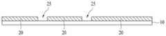
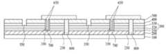
도 1a 내지 도 1g는 종래 복수 개의 단위셀이 직렬로 연결된 구조를 갖는 박막형 태양전지의 제조공정을 도시한 단면도이다.1A to 1G are cross-sectional views illustrating a manufacturing process of a thin film solar cell having a structure in which a plurality of conventional unit cells are connected in series.
우선, 도 1a에서 알 수 있듯이, 기판(10) 상에 ZnO와 같은 투명도전물을 이용하여 전면전극층(20a)을 형성한다.First, as shown in FIG. 1A, the
다음, 도 1b에서 알 수 있듯이, 상기 전면전극층(20a)의 소정 영역을 제거하여 제1분리부(25)를 형성한다. 그리하면, 상기 제1분리부(21)에 의해 이격되는 복수 개의 전면전극(20)이 형성된다.Next, as shown in FIG. 1B, the
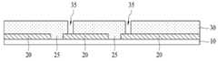
다음, 도 1c에서 알 수 있듯이, 상기 전면전극(20)을 포함한 기판(10) 전면에 반도체층(30a)을 형성한다.Next, as shown in FIG. 1C, the
다음, 도 1d에서 알 수 있듯이, 상기 반도체층(30a)의 소정 영역을 제거하여 콘택부(35)를 형성한다.Next, as shown in FIG. 1D, the
다음, 도 1e에서 알 수 있듯이, 상기 기판(10) 전면에 후면전극층(50a)을 형성한다.Next, as shown in FIG. 1E, a
다음, 도 1f에서 알 수 있듯이, 상기 후면전극층(50a) 및 반도체층(30)의 소정 영역을 제거하여 제2분리부(55)를 형성한다. 그리하면, 상기 제2분리부(55)에 의해 이격되며, 상기 콘택부(35)를 통해 전면전극(20)과 연결되는 복수 개의 후면전극(50)이 형성된다. 이와 같이 콘택부(35)를 통해 전면전극(20)과 후면전극(50)이 연결됨으로써 복수 개의 단위셀이 직렬로 연결되는 구조를 갖게 된다.Next, as shown in FIG. 1F, predetermined regions of the
그러나, 이와 같은 종래의 박막형 태양전지의 제조방법은 다음과 같은 문제점이 있다.However, the conventional method of manufacturing a thin film solar cell has the following problems.
종래의 제조방법을 간략히 요약하면, 종래의 제조방법은 전면전극층(20a)을 형성하는 공정(도 1a 참조), 제1분리부(25)를 형성하는 공정(도 1b 참조), 반도체층(30a)을 형성하는 공정(도 1c 참조), 콘택부(35)를 형성하는 공정(도 1d 참조), 후면전극층(50a)을 형성하는 공정(도 1e 참조), 및 제2분리부(55)를 형성하는 공정(도 1f 참조)으로 이루어진다.Briefly summarizing the conventional manufacturing method, the conventional manufacturing method is a step of forming the
이때, 상기 전면전극층(20a)을 형성하는 공정(도 1a 참조), 반도체층(30a)을 형성하는 공정(도 1c 참조), 및 후면전극층(50a)을 형성하는 공정(도 1e 참조)은 일반적으로 진공 증착 장비를 이용하여 수행하는 반면에, 상기 제1분리부(25)를 형성하는 공정(도 1b 참조), 콘택부(35)를 형성하는 공정(도 1d 참조), 및 제2분리부(55)를 형성하는 공정(도 1f 참조)은 대기압하에서 레이저 스크라이빙(Laser Scribing) 장비를 이용하여 수행하게 된다.In this case, the process of forming the
따라서, 종래의 경우 박막형 태양전지를 완성하기 위해서는 기판(10)을 진공 증착 장비와 레이저 스크라이빙 장비에 교대로 반복 투입해야 하는데, 이로 인해서 제조 장비 구성이 복잡하게 되고 제조 공정 시간이 오래 걸려 생산성이 떨어지는 문제점이 있다.Therefore, in the conventional case, in order to complete a thin-film solar cell, the
이와 같은 문제점에 대해서 보다 구체적으로 설명하면, 기판을 대기압하에서 진공 증착 장비 내로 투입하는 공정 시에는 외부의 공기가 진공 증착 장비 내부로 유입되는 것을 차단하기 위한 방안이 요구되는데, 일반적으로는 기판을 진공 증착 장비 내부로 직접 투입하지 않고 로드락 챔버(Load Rock Chamber)를 경유하도록 함으로써 외부의 공기가 진공 증착 장비 내부로 유입되지 않도록 하면서 기판을 진공 증착 장비 내부로 유입하게 된다.More specifically, this problem is required in the process of introducing the substrate into the vacuum deposition equipment under atmospheric pressure requires a method for blocking the outside air flow into the vacuum deposition equipment, generally the substrate vacuum The substrate is introduced into the vacuum deposition apparatus by preventing the outside air from flowing into the vacuum deposition apparatus by passing the load rock chamber without directly entering the deposition apparatus.
따라서, 종래와 같이 기판(10)을 진공 증착 장비와 레이저 스크라이빙 장비에 교대로 반복 투입하게 되면, 그만큼 로드락 챔버 등으로 인해 장비 구성이 복잡하게 되고, 또한 로드락 챔버를 경유하는 만큼 제조 공정 시간이 오래 걸리게 되는 문제점이 있다.Therefore, if the
본 발명은 전술한 종래의 박막형 태양전지의 문제점을 해결하기 위해 고안된 것으로서,The present invention is designed to solve the problems of the conventional thin-film solar cell described above,
본 발명은 필요한 증착 공정을 모두 수행하고 그 후에 스크라이빙 공정을 수행함으로써 기판을 진공 증착 장비와 레이저 스크라이빙 장비에 교대로 반복 투입하지 않도록 하여 제조 장비 구성이 단순하게 되고, 제조 공정 시간도 단축될 수 있는 박막형 태양전지 및 그 제조방법을 제공하는 것을 목적으로 한다.According to the present invention, by performing all the necessary deposition processes and then performing a scribing process, the configuration of the manufacturing equipment is simplified by not repeatedly injecting the substrate into the vacuum deposition equipment and the laser scribing equipment. An object of the present invention is to provide a thin film solar cell and a method of manufacturing the same.
본 발명은 상기 목적을 달성하기 위해서, 기판 위에 전면전극층, 광전변환부 및 후면전극층을 차례로 적층하는 공정; 상기 전면전극층, 광전변환부 및 후면전극층의 소정 영역을 제거하여 제1분리부를 형성하는 공정; 상기 광전변환부 및 후면전극층의 소정 영역을 제거하여 콘택부를 형성하는 공정; 상기 후면전극층의 소정 영역을 제거하여 제2분리부를 형성하는 공정; 및 상기 콘택부를 통해 상기 전면전극층과 후면전극층을 전기적으로 연결하는 금속층을 형성하는 공정을 포함하여 이루어진 것을 특징으로 하는 박막형 태양전지의 제조방법을 제공한다.The present invention, in order to achieve the above object, a step of sequentially stacking a front electrode layer, a photoelectric conversion unit and a back electrode layer on a substrate; Forming a first separator by removing predetermined regions of the front electrode layer, the photoelectric conversion part, and the back electrode layer; Forming a contact part by removing predetermined regions of the photoelectric conversion part and the back electrode layer; Removing a predetermined region of the back electrode layer to form a second separator; And forming a metal layer electrically connecting the front electrode layer and the back electrode layer through the contact portion.
상기 광전변환부는 PIN구조의 반도체층으로 형성할 수 있다.The photoelectric conversion unit may be formed of a semiconductor layer having a PIN structure.
상기 광전변환부는 PIN구조의 제1반도체층, 상기 제1반도체층 상에 형성된 버퍼층, 및 상기 버퍼층 상에 형성된 PIN구조의 제2반도체층으로 형성할 수 있으며, 이때, 상기 제1반도체층은 비정질 반도체물질로 형성하고, 상기 버퍼층은 투명 도전물로 형성하고, 상기 제2반도체층은 미세결정질 반도체물질로 형성할 수 있다.The photoelectric conversion unit may be formed of a first semiconductor layer having a PIN structure, a buffer layer formed on the first semiconductor layer, and a second semiconductor layer having a PIN structure formed on the buffer layer, wherein the first semiconductor layer is amorphous. The semiconductor layer may be formed of a semiconductor material, the buffer layer may be formed of a transparent conductive material, and the second semiconductor layer may be formed of a microcrystalline semiconductor material.
상기 금속층을 형성하는 공정 이전에 상기 제1분리부에 절연층을 형성하는 공정을 추가로 포함할 수 있다.The method may further include forming an insulating layer on the first separation unit before forming the metal layer.
상기 광전변화부를 제1반도체층, 버퍼층, 및 제2반도체층으로 형성할 경우에 있어서, 상기 금속층을 형성하는 공정 이전에 상기 콘택부의 양 측면에 제2절연층을 형성하는 공정을 추가로 포함할 수 있으며, 이때, 상기 제2절연층은 상기 금속층과 상기 버퍼층 사이에 형성할 수 있다.In the case of forming the photoelectric change part as the first semiconductor layer, the buffer layer, and the second semiconductor layer, the method may further include forming a second insulating layer on both sides of the contact portion before forming the metal layer. In this case, the second insulating layer may be formed between the metal layer and the buffer layer.
상기 금속층은 상기 제1분리부에 의해 이격된 후면전극층 사이를 연결하도록 형성할 수 있다.The metal layer may be formed to connect between the rear electrode layers spaced by the first separator.
상기 콘택부는 상기 제1분리부와 상기 제2분리부 사이의 영역에 형성할 수 있다.The contact portion may be formed in a region between the first separator and the second separator.
상기 광전변환부와 후면전극층 사이에 투명도전층을 형성하는 공정을 추가로 포함하고, 상기 제1분리부, 콘택부 및 제2분리부 형성시 상기 투명도전층의 소정 영역도 함께 제거할 수 있다.The method may further include forming a transparent conductive layer between the photoelectric conversion unit and the back electrode layer, and may also remove a predetermined region of the transparent conductive layer when the first separation unit, the contact unit, and the second separation unit are formed.
본 발명은 또한, 기판 위에 제1분리부에 의해 이격 형성되는 전면전극; 상기 전면전극 위에서, 콘택부를 구비하여 형성되는 광전변환부; 상기 광전변환부 위에서, 제2분리부에 의해 이격 형성되며 상기 콘택부를 구비하여 형성되는 후면전극; 및 상기 콘택부를 통해 상기 전면전극과 후면전극을 전기적으로 연결시키는 금속층을 포함하여 이루어진 박막형 태양전지를 제공한다.The present invention also includes a front electrode spaced apart from the first separation portion on the substrate; A photoelectric conversion part formed on the front electrode with a contact part; A back electrode formed on the photoelectric conversion part, spaced apart by a second separation part, and including the contact part; And a metal layer electrically connecting the front electrode and the rear electrode through the contact part.
상기 광전변환부는 PIN구조의 반도체층으로 이루어질 수 있다.The photoelectric conversion unit may be formed of a semiconductor layer having a PIN structure.
상기 광전변환부는 PIN구조의 제1반도체층, 상기 제1반도체층 상에 형성된 버퍼층, 및 상기 버퍼층 상에 형성된 PIN구조의 제2반도체층으로 이루어질 수 있고, 이때, 상기 제1반도체층은 비정질 반도체물질로 이루어지고, 상기 버퍼층은 투명도전물로 이루어지고, 상기 제2반도체층은 미세결정질 반도체물질로 이루어질 수 있다.The photoelectric conversion unit may include a first semiconductor layer having a PIN structure, a buffer layer formed on the first semiconductor layer, and a second semiconductor layer having a PIN structure formed on the buffer layer, wherein the first semiconductor layer is an amorphous semiconductor. It may be made of a material, the buffer layer may be made of a transparent conductive material, and the second semiconductor layer may be made of a microcrystalline semiconductor material.
상기 광전변환부 및 후면전극은 상기 제1분리부를 구비하여 형성되며, 이때, 상기 제1분리부에는 절연층이 형성되고, 상기 금속층은 상기 제1분리부에 의해 이격된 후면전극 사이를 연결할 수 있다.The photoelectric conversion unit and the back electrode are formed to include the first separation unit, wherein an insulating layer is formed on the first separation unit, and the metal layer can be connected between the rear electrodes spaced apart by the first separation unit. have.
상기 광전변화부가 제1반도체층, 버퍼층, 및 제2반도체층으로 이루어진 경우에 있어서, 상기 콘택부의 양 측면에 제2절연층이 형성될 수 있고, 이때, 상기 제2절연층은 상기 금속층과 상기 버퍼층 사이에 형성될 수 있다.When the photoelectric change part is formed of a first semiconductor layer, a buffer layer, and a second semiconductor layer, second insulating layers may be formed on both side surfaces of the contact part, wherein the second insulating layer is formed of the metal layer and the second insulating layer. It may be formed between the buffer layer.
상기 콘택부는 상기 제1분리부와 상기 제2분리부 사이의 영역에 형성될 수 있다.The contact portion may be formed in a region between the first separator and the second separator.
상기 광전변환부와 후면전극 사이에 상기 후면전극과 동일한 패턴의 투명도전층이 추가로 형성될 수 있다.A transparent conductive layer having the same pattern as that of the back electrode may be further formed between the photoelectric converter and the back electrode.
상기와 같은 본 발명에 따르면, 기판 위에 전면전극층, 광전변환부 및 후면전극층을 차례로 적층하고, 그 후에, 제1분리부, 콘택부 및 제2분리부를 형성하기 때문에, 종래와 같이 진공 증착 장비와 레이저 스크라이빙 장비를 교대로 반복 이용할 필요가 없어 제조 장비 구성이 단순하게 되고, 제조 공정 시간도 단축되어 생 산성이 향상된다.According to the present invention as described above, since the front electrode layer, the photoelectric conversion unit and the rear electrode layer are sequentially stacked on the substrate, and then the first separation unit, the contact unit and the second separation unit are formed, the vacuum deposition apparatus and the conventional There is no need to alternately use laser scribing equipment, which simplifies manufacturing equipment construction and shortens the manufacturing process time, thus improving productivity.
이하, 도면을 참조로 본 발명의 바람직한 실시예에 대해서 상세히 설명하기로 한다.Hereinafter, exemplary embodiments of the present invention will be described in detail with reference to the accompanying drawings.
<박막형 태양전지 제조방법><Thin Film Solar Cell Manufacturing Method>
도 2a 내지 도 2d는 본 발명의 일 실시예에 따른 박막형 태양전지의 제조공정을 도시한 단면도이다.2A to 2D are cross-sectional views illustrating a manufacturing process of a thin film solar cell according to an embodiment of the present invention.
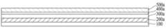
우선, 도 2a에서 알 수 있듯이, 기판(100) 위에 전면전극층(200a), 광전변환부(300a), 투명도전층(400a) 및 후면전극층(500a)을 차례로 적층한다.First, as shown in FIG. 2A, the
상기 기판(100)으로는 유리 또는 투명한 플라스틱을 이용할 수 있다.Glass or transparent plastic may be used as the
상기 전면전극층(200a)은 ZnO, ZnO:B, ZnO:Al, SnO2, SnO2:F, ITO(Indium Tin Oxide), 등과 같은 투명한 도전물질을 스퍼터링(Sputtering)법 또는 MOCVD(Metal Organic Chemical Vapor Deposition)법 등을 이용하여 적층할 수 있다.The
상기 전면전극층(200a)은 태양광이 입사되는 면이기 때문에 입사되는 태양광이 태양전지 내부로 최대한 흡수될 수 있도록 하는 것이 중요하며, 이를 위해서 상기 전면전극층(200a)에 텍스처(texturing) 가공공정을 추가로 수행할 수 있다. 상기 텍스처 가공공정이란 물질 표면을 울퉁불퉁한 요철구조로 형성하여 마치 직물의 표면과 같은 형상으로 가공하는 공정으로서, 포토리소그라피법(photolithography)을 이용한 식각공정, 화학용액을 이용한 이방성 식각공정(anisotropic etching), 또는 기계적 스크라이빙(mechanical scribing)을 이용한 홈 형성 공정 등을 통해 수행할 수 있다. 이와 같은 텍스처 가공공정을 상기 전면전극층(200a)에 수행할 경우 입사되는 태양광이 태양전지 외부로 반사되는 비율은 감소하게 되며, 그와 더불어 입사되는 태양광의 산란에 의해 태양전지 내부로 태양광이 흡수되는 비율은 증가하게 되어, 태양전지의 효율이 증진되는 효과가 있다.Since the
상기 광전변환부(300a)는 실리콘계 반도체물질을 플라즈마 CVD법 등을 이용하여 적층할 수 있으며, P형 반도체층, I형 반도체층 및 N형 반도체층이 순서대로 적층된 PIN구조로 형성할 수 있다. 이와 같이 상기 광전변환부(300a)를 PIN구조로 형성하게 되면, I형 반도체층이 P형 반도체층과 N형 반도체층에 의해 공핍(depletion)이 되어 내부에 전기장이 발생하게 되고, 태양광에 의해 생성되는 정공 및 전자가 상기 전기장에 의해 드리프트(drift)되어 각각 P형 반도체층 및 N형 반도체층에서 수집되게 된다. 한편, 상기 광전변환부(300a)를 PIN구조로 형성할 경우에는 P형 반도체층을 먼저 형성하고, 그 후에 I형 반도체층 및 N형 반도체층을 순서대로 형성하는 것이 바람직한데, 그 이유는 일반적으로 정공의 드리프트 이동도(drift mobility)가 전자의 드리프트 이동도에 의해 낮기 때문에 입사광에 의한 수집효율을 극대화하기 위해서 P형 반도체층을 수광면에 가깝게 형성하기 위함이다.The
상기 투명도전층(400a)은 ZnO, ZnO:B, ZnO:Al, Ag와 같은 투명한 도전물질을 스퍼터링(Sputtering)법 또는 MOCVD(Metal Organic Chemical Vapor Deposition)법 등을 이용하여 적층할 수 있다. 상기 투명도전층(400a)은 생략하는 것도 가능하지 만, 태양전지의 효율증진을 위해서는 상기 투명도전층(400a)을 형성하는 것이 바람직하다. 즉, 상기 투명도전층(400a)을 형성하게 되면 상기 광전변환부(300a)를 투과한 태양광이 투명도전층(400a)을 통과하면서 산란을 통해 다양한 각으로 진행하게 되어 상기 후면전극층(500a)에서 반사되어 광전변환부(300a)로 재입사되는 광의 비율이 증가될 수 있기 때문이다.The transparent
상기 후면전극층(500a)은 Ag, Al, Ag+Mo, Ag+Ni, Ag+Cu 등과 같은 금속을 스퍼터링(Sputtering)법 등을 이용하여 적층할 수 있으며, 경우에 따라서 스크린 인쇄법을 이용하여 적층할 수도 있다.The
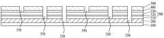
다음, 도 2b에서 알 수 있듯이, 제1분리부(250), 콘택부(350), 및 제2분리부(550)를 형성하여, 전면전극(200), 광전변환부(300), 투명도전층(400), 및 후면전극(500)을 완성한다.Next, as shown in FIG. 2B, the
상기 제1분리부(250)는 상기 전면전극(200)을 소정 간격으로 이격시켜 박막 태양전지를 단위셀로 분리하는 역할을 하는 것으로서, 상기 제1분리부(250)는 상기 전면전극층(200a), 광전변환부(300a), 투명도전층(400a) 및 후면전극층(500a)의 소정 영역을 제거하여 형성한다.The
상기 콘택부(350)는 상기 전면전극(200)과 후면전극(500)을 전기적으로 연결하는 연결 통로로서 박막 태양전지의 단위셀 간을 직렬로 연결할 수 있도록 하는 역할을 하는 것으로서, 상기 콘택부(350)는 상기 광전변환부(300a), 투명도전층(400a) 및 후면전극층(500a)의 소정 영역을 제거하여 형성한다. 또한, 상기 콘택부(350)는 상기 제1분리부(250)와 제2분리부(550) 사이의 영역에 형성한다.The
상기 제2분리부(550)는 상기 후면전극(500)을 소정 간격으로 이격시켜 박막 태양전지를 단위셀로 분리하는 역할을 하는 것으로서, 상기 제2분리부(550)는 상기 투명도전층(400a) 및 후면전극층(500a)의 소정 영역을 제거하여 형성한다.The
상기 제1분리부(250), 콘택부(350) 및 제2분리부(550)는 레이저 스크라이빙 공정을 이용하여 형성할 수 있으며, 서로 간에 특별한 공정 순서가 요하지 않는다. 즉, 상기 제1분리부(250), 콘택부(350) 및 제2분리부(550) 중 어느 하나를 먼저 형성하고, 그 이후에 나머지 두 개를 차례로 형성하면 되고, 레이저 스크라이빙 장비의 구조 변경을 통해서 상기 제1분리부(250), 콘택부(350) 및 제2분리부(550) 중 어느 두 개를 동시에 형성하거나 아니면 세 개를 동시에 형성할 수 있을 경우 공정시간 단축에 유리하게 된다.The
다음, 도 2c에서 알 수 있듯이, 상기 제1분리부(250)에 제1절연층(600)을 형성한다.Next, as shown in FIG. 2C, a first insulating
상기 제1절연층(600)은 단위셀로 분리된 전면전극(200)들이 후술하는 공정에서 서로 전기적으로 연결되는 것을 방지하기 위해 형성하는 것이다. 구체적으로 설명하면, 후술하는 도 2d공정에서는 상기 콘택부(350)를 통해 상기 전면전극(200)과 후면전극(500)을 전기적으로 연결하기 위해서 금속층(700)을 형성하게 되는데, 이때 금속층(700)이 상기 제1분리부(250) 내로 침투하게 되면 단위셀로 분리된 전면전극(200)들이 상기 금속층(700)에 의해 전기적으로 연결되어 쇼트가 발생하게 된다.The first insulating
따라서, 단위셀로 분리된 전면전극(200)들이 금속층(700)에 의해 전기적으로 연결되는 것을 방지하기 위해서 금속층(700) 형성 전에 제1분리부(250)에 제1절연층(600)을 형성하는 것이다. 한편, 상기 제1절연층(600)은 단위셀로 분리된 전면전극(200)들이 전기적으로 연결되는 것을 방지하기 위한 것이기 때문에, 반드시 상기 제1분리부(250)의 내부 전체에 제1절연층(600)을 형성할 필요는 없으며, 상기 제1분리부(250) 내부에서 상기 전면전극(200)과 동일한 높이 이상으로 제1절연층(600)을 형성하면 된다.Therefore, in order to prevent the
다음, 도 2d에서 알 수 있듯이, 상기 콘택부(350)를 통해 상기 전면전극(200)과 후면전극(500)을 전기적으로 연결하는 금속층(700)을 형성한다.Next, as can be seen in Figure 2d, through the
상기 금속층(700)은 상기 전면전극(200)과 후면전극(500)을 전기적으로 연결함으로써 박막 태양전지의 단위셀 간을 직렬로 연결하는 것이다.The
한편, 상기 제1분리부(250)는 전면전극(200)을 단위셀로 분리하는 것이지만, 공정상 상기 제1분리부(250)에 의해 후면전극(500) 또한 분리되어 이격되며, 이와 같이 제1분리부(250)에 의해 이격된 후면전극(500)을 상기 금속층(700)을 통해 연결함으로써 하나의 단위셀 내에서 후면전극(500) 전체가 전기적으로 연결될 수 있다.Meanwhile, the
도 3a 내지 도 3d는 본 발명의 다른 실시예에 따른 박막형 태양전지의 제조공정을 도시한 단면도로서, 이는 탠덤(Tandem)구조의 박막형 태양전지의 제조공정에 관한 것이다. 전술한 실시예와 동일한 구성에 대해서는 동일한 도면부호를 부여하였고, 동일한 구성에 대한 구체적인 설명은 생략하기로 한다.3A to 3D are cross-sectional views illustrating a manufacturing process of a thin film solar cell according to another embodiment of the present invention, which relates to a manufacturing process of a tandem thin film solar cell. The same reference numerals are given to the same elements as in the above-described embodiment, and detailed descriptions of the same elements will be omitted.
우선, 도 3a에서 알 수 있듯이, 기판(100) 위에 전면전극층(200a), 광전변환 부(300a), 투명도전층(400a) 및 후면전극층(500a)을 차례로 적층한다.First, as shown in FIG. 3A, the
상기 광전변환부(300a)를 적층하는 공정은 제1반도체층(310a)을 적층하고, 상기 제1반도체층(310a) 상에 버퍼층(320a)을 적층하고, 그리고 상기 버퍼층(320a) 상에 제2반도체층(330a)을 적층하는 공정으로 이루어진다.The process of stacking the
상기 제1반도체층(310a)은 PIN구조의 비정질 반도체물질로 이루어지고, 상기 제2반도체층(330a)은 미세결정질 반도체물질로 이루어질 수 있다.The
상기 비정질 반도체물질은 단파장의 광을 잘 흡수하고 상기 미세결정질 반도체물질은 장파장의 광을 잘 흡수하는 특성이 있기 때문에, 비정질 반도체물질과 미세결정질 반도체물질을 조합하여 광전변환부(300a)를 형성함으로써 광흡수효율이 증진될 수 있다. 또한, 비정질 반도체물질은 장시간 빛에 노출될 경우 열화현상이 가속되는 문제가 있는데, 비정질 반도체물질을 태양광이 입사되는 면에 형성하고 미세결정질 반도체물질을 그 반대면에 형성할 경우 태양전지의 열화를 줄일 수 있는 효과가 있다. 따라서, 태양광이 입사되는 면에서 가까운 제1반도체층(310a)을 비정질 반도체물질로 형성하고, 태양광이 입사되는 면에서 먼 제2반도체층(330a)을 미세결정질 반도체물질로 형성할 수 있다. 다만, 반드시 이에 한정되는 것은 아니고, 상기 제2반도체층(330a)으로서 비정질 반도체물질, 비정질실리콘/게르마늄 물질 등 다양하게 변경 이용할 수도 있다.Since the amorphous semiconductor material absorbs light of short wavelength well and the microcrystalline semiconductor material absorbs light of long wavelength well, the
상기 버퍼층(320a)은 상기 제1반도체층(310a)과 제2반도체층(330a) 사이에 형성되어, 상기 제1반도체층(310a)과 제2반도체층(330a) 사이에서 터널접합을 통해 정공 및 전자의 이동을 원활히 하는 역할을 한다. 즉, 상기 제1반도체층(310a)에서 생성된 전자가 상기 제2반도체층(330a)으로 이동하기 위해서는 상기 제1반도체층(310a) 및 제2반도체층(330a) 사이에서 터널링 과정을 거처야 하며, 이를 위해서 버퍼층(320a)을 형성하는 것이다. 상기 버퍼층(320a)은 ZnO와 같은 투명한 도전물질을 이용하여 형성한다.The
다음, 도 3b에서 알 수 있듯이, 제1분리부(250), 콘택부(350), 및 제2분리부(550)를 형성하여, 전면전극(200), 광전변환부(300), 투명도전층(400), 및 후면전극(500)을 완성한다.Next, as shown in FIG. 3B, the
다음, 도 3c에서 알 수 있듯이, 상기 제1분리부(250)에 제1절연층(600)을 형성하고, 상기 콘택부(350)의 양 측면에 제2절연층(650)을 형성한다.Next, as shown in FIG. 3C, the first insulating
상기 제1절연층(600)은 단위셀로 분리된 전면전극(200)들이 후술하는 도 3d 공정에서 금속층(700)에 의해 서로 전기적으로 연결되는 것을 방지하기 위해 형성하는 것임은 전술한 바와 동일하다.The first insulating
상기 제2절연층(650)은 후술하는 도 3d공정에서 금속층(700)과 버퍼층(320)이 전기적으로 연결되어 쇼트가 발생하는 것을 차단하는 역할을 하는 것이다. 즉, 도 4d공정에서 금속층(700)이 전면전극(200)과 이웃하는 후면전극(500)을 전기적으로 연결시킬 때, 상기 금속층(700)이 상기 광전변환부(300) 내의 투명한 도전물질로 이루어진 버퍼층(320)과 접촉하게 되면 쇼트가 발생하게 되므로, 금속층(700)과 버퍼층(320)이 접촉하는 것을 차단하기 위해서 제2절연층(650)을 형성하는 것이다.The second
따라서, 상기 제2절연층(650)은 상기 콘택부(350)의 양 측면, 즉 상기 콘택부(350) 내에서 상기 버퍼층(320)과 접촉하도록 형성함으로써, 결과적으로 도 3d공 정 이후에 상기 금속층(700)과 버퍼층(320) 사이에 제2절연층(650)이 형성되도록 한다.Accordingly, the second insulating
다음, 도 3d에서 알 수 있듯이, 상기 콘택부(350)를 통해 상기 전면전극(200)과 후면전극(500)을 전기적으로 연결하는 금속층(700)을 형성한다.Next, as can be seen in Figure 3d, through the
<박막형 태양전지><Thin Film Solar Cell>
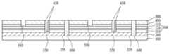
도 4는 본 발명의 일 실시예에 따른 박막형 태양전지의 개략적인 단면도이다.4 is a schematic cross-sectional view of a thin film solar cell according to an embodiment of the present invention.
도 4에서 알 수 있듯이, 본 발명의 일 실시예에 따른 박막형 태양전지는 기판(100), 전면전극(200), 광전변환부(300), 투명도전층(400), 후면전극(500), 제1절연층(600) 및 금속층(700)을 포함하여 이루어진다.As can be seen in Figure 4, the thin-film solar cell according to an embodiment of the present invention, the
상기 전면전극(200)은 상기 기판(100) 위에 형성되며, 제1분리부(250)에 의해 이격 형성된다. 상기 전면전극(200)은 ZnO, ZnO:B, ZnO:Al, SnO2, SnO2:F, ITO(Indium Tin Oxide) 등과 같은 투명한 도전물질로 이루어질 수 있으며, 태양광의 흡수율을 증진시키기 위해서 그 표면이 요철구조로 형성될 수 있다.The
상기 광전변환부(300)는 상기 전면전극(200) 위에 형성되며, 제1분리부(250) 및 콘택부(350)를 구비하여 형성된다. 상기 광전변환부(300)는 P형 반도체층, I형 반도체층 및 N형 반도체층이 순서대로 적층된 PIN구조의 실리콘계 반도체물질로 이루어질 수 있다.The
상기 투명도전층(400)은 상기 광전변환부(300) 위에 형성되며, 상기 후면전극(500)과 동일한 패턴으로 형성된다. 상기 투명도전층(400)은 ZnO, ZnO:B, ZnO:Al, Ag와 같은 투명한 도전물질로 이루어질 수 있으며, 경우에 따라서 생략할 수도 있다.The transparent
상기 후면전극(500)은 상기 투명도전층(400) 위에 형성되며, 제2분리부(550)에 의해 이격 형성된다. 하나의 단위셀을 구성하는 하나의 후면전극(500)은 제1분리부(250) 및 콘택부(350)에 의해서 이격된 모습을 보이지만, 상기 금속층(700)에 의해서 전기적으로 연결된 구조를 이룬다. 상기 후면전극(500)은 Ag, Al, Ag+Mo, Ag+Ni, Ag+Cu 등과 같은 금속으로 이루어질 수 있다.The
상기 제1절연층(600)은 이격 형성된 전면전극(200)들이 전기적으로 연결되는 것을 방지하기 위해서, 상기 제1분리부(250)에 형성된다. 상기 제1절연층(600)은 반드시 상기 제1분리부(250)의 내부 전체에 형성될 필요는 없으며, 상기 제1분리부(250) 내부에서 상기 전면전극(200)과 동일한 높이 이상으로 형성되면 된다.The first insulating
상기 금속층(700)은 상기 콘택부(350)를 통해 상기 전면전극(200)과 후면전극(500)을 전기적으로 연결시킨다. 또한, 상기 금속층(700)은 상기 제1분리부(250)에 의해 이격된 후면전극(500)을 연결함으로써 하나의 단위셀 내에서 후면전극(500) 전체가 전기적으로 연결될 수 있도록 한다.The
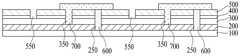
도 5는 본 발명의 다른 실시예에 따른 박막형 태양전지의 단면도로서, 이는 탠덤(Tandem)구조의 박막형 태양전지에 관한 것이다. 전술한 실시예와 동일한 구성에 대해서는 동일한 도면부호를 부여하였고, 동일한 구성에 대한 구체적인 설명은 생략하기로 한다.5 is a cross-sectional view of a thin film solar cell according to another embodiment of the present invention, which relates to a thin film solar cell having a tandem structure. The same reference numerals are given to the same elements as in the above-described embodiment, and detailed descriptions of the same elements will be omitted.
도 5에서 알 수 있듯이, 본 발명의 다른 실시예에 따른 박막형 태양전지는 기판(100), 전면전극(200), 광전변환부(300), 투명도전층(400), 후면전극(500), 제1절연층(600), 제2절연층(650) 및 금속층(700)을 포함하여 이루어진다.As can be seen in Figure 5, the thin-film solar cell according to another embodiment of the present invention, the
상기 광전변환부(300)는 제1반도체층(310), 상기 제1반도체층(310) 상에 형성된 버퍼층(320), 및 상기 버퍼층(320) 상에 형성된 제2반도체층(330)으로 이루어진다. 상기 제1반도체층(310)은 PIN구조의 비정질 반도체물질로 이루어지고, 상기 버퍼층(320)은 ZnO와 같은 투명한 도전물질로 이루어지고, 상기 제2반도체층(330)은 미세결정질 반도체물질로 이루어질 수 있다. 다만, 반드시 이에 한정되는 것은 아니고, 상기 제2반도체층(330)으로서 비정질 반도체물질, 비정질실리콘/게르마늄 물질 등 다양하게 변경 이용할 수도 있다.The
상기 제2절연층(350)은 콘택부(350)의 양 측면에, 구체적으로는 상기 금속층(700)과 버퍼층(320) 사이에 형성되어, 상기 금속층(700)과 버퍼층(320) 사이에 쇼트가 발생하는 것을 방지한다.The second
이상 도 4 및 도 5에 따른 박막형 태양전지는 각각 전술한 도 2a 내지 도 2d 및 도 3a 내지 도 3d에 따른 방법에 의해 제조될 수 있지만, 반드시 그 방법에 한정되는 것은 아니다.The thin film solar cell according to FIGS. 4 and 5 may be manufactured by the method of FIGS. 2A to 2D and 3A to 3D, respectively, but is not necessarily limited thereto.
도 1a 내지 도 1f는 종래의 박막형 태양전지의 제조공정을 도시한 단면도이다.1A to 1F are cross-sectional views illustrating a manufacturing process of a conventional thin film solar cell.
도 2a 내지 도 2d는 본 발명의 일 실시예에 따른 박막형 태양전지의 제조공정을 도시한 단면도이다.2A to 2D are cross-sectional views illustrating a manufacturing process of a thin film solar cell according to an embodiment of the present invention.
도 3a 내지 도 3d는 본 발명의 다른 실시예에 따른 박막형 태양전지의 제조공정을 도시한 단면도이다.3A to 3D are cross-sectional views illustrating a manufacturing process of a thin film solar cell according to another embodiment of the present invention.
도 4는 본 발명의 일 실시예에 따른 박막형 태양전지의 단면도이다.4 is a cross-sectional view of a thin film solar cell according to an embodiment of the present invention.
도 5는 본 발명의 일 실시예에 따른 박막형 태양전지의 단면도이다.5 is a cross-sectional view of a thin film solar cell according to an embodiment of the present invention.
<도면의 주요부의 부호에 대한 설명><Description of Signs of Major Parts of Drawing>
100: 기판 200: 전면전극100: substrate 200: front electrode
250: 제1분리부 300: 광전변환부250: first separation unit 300: photoelectric conversion unit
310: 제1반도체층 320: 버퍼층310: first semiconductor layer 320: buffer layer
330: 제2반도체층 350: 콘택부330: second semiconductor layer 350: contact portion
400: 투명도전층 500: 후면전극400: transparent conductive layer 500: rear electrode
550: 제2분리부 600: 제1절연층550: second separator 600: first insulating layer
650: 제2절연층 700: 금속층650: second insulating layer 700: metal layer
Claims (21)
Translated fromKoreanPriority Applications (1)
| Application Number | Priority Date | Filing Date | Title |
|---|---|---|---|
| KR1020140079565AKR101457010B1 (en) | 2008-07-10 | 2014-06-27 | Thin film type Solar Cell, and Method for manufacturing the same |
Applications Claiming Priority (2)
| Application Number | Priority Date | Filing Date | Title |
|---|---|---|---|
| KR1020080051659 | 2008-06-02 | ||
| KR20080051659 | 2008-06-02 |
Related Child Applications (1)
| Application Number | Title | Priority Date | Filing Date |
|---|---|---|---|
| KR1020140079565ADivisionKR101457010B1 (en) | 2008-07-10 | 2014-06-27 | Thin film type Solar Cell, and Method for manufacturing the same |
Publications (3)
| Publication Number | Publication Date |
|---|---|
| KR20090125675Atrue KR20090125675A (en) | 2009-12-07 |
| KR101457573B1 KR101457573B1 (en) | 2014-11-03 |
| KR101457573B9 KR101457573B9 (en) | 2024-12-20 |
Family
ID=41687148
Family Applications (1)
| Application Number | Title | Priority Date | Filing Date |
|---|---|---|---|
| KR1020080066931AActiveKR101457573B1 (en) | 2008-06-02 | 2008-07-10 | Thin film solar cell and its manufacturing method |
Country Status (1)
| Country | Link |
|---|---|
| KR (1) | KR101457573B1 (en) |
Cited By (5)
| Publication number | Priority date | Publication date | Assignee | Title |
|---|---|---|---|---|
| KR101039148B1 (en)* | 2010-03-31 | 2011-06-07 | 주식회사 티지솔라 | Solar cell and manufacturing method |
| WO2012046936A1 (en)* | 2010-10-05 | 2012-04-12 | 엘지이노텍주식회사 | Photovoltaic power generation device and manufacturing method thereof |
| WO2013058524A1 (en)* | 2011-10-18 | 2013-04-25 | Lg Innotek Co., Ltd. | Solar cell apparatus and method of fabricating the same |
| KR101393743B1 (en)* | 2012-06-28 | 2014-05-13 | 엘지이노텍 주식회사 | Solar cell and method of fabricating the same |
| KR101393859B1 (en)* | 2012-06-28 | 2014-05-13 | 엘지이노텍 주식회사 | Solar cell and method of fabricating the same |
Family Cites Families (3)
| Publication number | Priority date | Publication date | Assignee | Title |
|---|---|---|---|---|
| AU8872891A (en)* | 1990-10-15 | 1992-05-20 | United Solar Systems Corporation | Monolithic solar cell array and method for its manufacture |
| US8455753B2 (en)* | 2005-01-14 | 2013-06-04 | Semiconductor Energy Laboratory Co., Ltd. | Solar cell and semiconductor device, and manufacturing method thereof |
| KR100833675B1 (en)* | 2007-01-30 | 2008-05-29 | (주)실리콘화일 | Translucent Crystalline Silicon Thin Film Solar Cell |
- 2008
- 2008-07-10KRKR1020080066931Apatent/KR101457573B1/enactiveActive
Cited By (8)
| Publication number | Priority date | Publication date | Assignee | Title |
|---|---|---|---|---|
| KR101039148B1 (en)* | 2010-03-31 | 2011-06-07 | 주식회사 티지솔라 | Solar cell and manufacturing method |
| WO2012046936A1 (en)* | 2010-10-05 | 2012-04-12 | 엘지이노텍주식회사 | Photovoltaic power generation device and manufacturing method thereof |
| CN103069574A (en)* | 2010-10-05 | 2013-04-24 | Lg伊诺特有限公司 | Photovoltaic power generation device and manufacturing method thereof |
| CN103069574B (en)* | 2010-10-05 | 2016-04-20 | Lg伊诺特有限公司 | Photovoltaic power generation equipment and manufacture method thereof |
| WO2013058524A1 (en)* | 2011-10-18 | 2013-04-25 | Lg Innotek Co., Ltd. | Solar cell apparatus and method of fabricating the same |
| US9559223B2 (en) | 2011-10-18 | 2017-01-31 | Lg Innotek Co., Ltd. | Solar cell apparatus and method of fabricating the same |
| KR101393743B1 (en)* | 2012-06-28 | 2014-05-13 | 엘지이노텍 주식회사 | Solar cell and method of fabricating the same |
| KR101393859B1 (en)* | 2012-06-28 | 2014-05-13 | 엘지이노텍 주식회사 | Solar cell and method of fabricating the same |
Also Published As
| Publication number | Publication date |
|---|---|
| KR101457573B9 (en) | 2024-12-20 |
| KR101457573B1 (en) | 2014-11-03 |
Similar Documents
| Publication | Publication Date | Title |
|---|---|---|
| KR101463925B1 (en) | Thin film type Solar Cell, and Method for manufacturing the same | |
| KR101301664B1 (en) | The method for manufacturing Thin film type Solar Cell, and Thin film type Solar Cell made by the method | |
| KR101460580B1 (en) | Thin film type Solar Cell, and Method for manufacturing the same | |
| KR20110029585A (en) | Thin film type solar cell, manufacturing method thereof, and thin film type solar cell module and solar power generation system using same | |
| KR20100021045A (en) | Thin film type solar cell and method for manufacturing the same | |
| KR20090068110A (en) | Thin film type solar cell and manufacturing method thereof | |
| KR101676368B1 (en) | Solar Cell and method of manufacturing the same | |
| KR20170030311A (en) | A thin film type solar cell and Method of manufacturing the same | |
| KR101405023B1 (en) | Thin film solar cell and its manufacturing method | |
| KR20090073308A (en) | Thin film type solar cell and manufacturing method thereof | |
| KR101457573B1 (en) | Thin film solar cell and its manufacturing method | |
| KR101368903B1 (en) | Thin film type Solar Cell, and Method for manufacturing the same | |
| KR101114217B1 (en) | Thin film type Solar Cell, and Method for manufacturing the same | |
| KR101476125B1 (en) | Thin film solar cell and its manufacturing method | |
| KR101460619B1 (en) | Thin film solar cell and its manufacturing method | |
| KR101415322B1 (en) | Thin film solar cell and its manufacturing method | |
| KR101457010B1 (en) | Thin film type Solar Cell, and Method for manufacturing the same | |
| KR20120034308A (en) | Thin film type solar cell and method for manufacturing the same | |
| KR101073832B1 (en) | Method for manufacturing thin film type Solar Cell | |
| KR20120139177A (en) | Solar cell and method for manufacturing the same | |
| KR101562346B1 (en) | Method of manufacturing Thin film type Solar Cell | |
| KR101527405B1 (en) | Manufacturing System of Thin Film Solar Cell | |
| KR101512114B1 (en) | Thin film solar cell and its manufacturing method | |
| KR101528455B1 (en) | Thin film type Solar Cell and Method for manufacturing the same | |
| KR20100037861A (en) | Thin film type solar cell and method for manufacturing the same |
Legal Events
| Date | Code | Title | Description |
|---|---|---|---|
| PA0109 | Patent application | Patent event code:PA01091R01D Comment text:Patent Application Patent event date:20080710 | |
| PG1501 | Laying open of application | ||
| A201 | Request for examination | ||
| PA0201 | Request for examination | Patent event code:PA02012R01D Patent event date:20130603 Comment text:Request for Examination of Application Patent event code:PA02011R01I Patent event date:20080710 Comment text:Patent Application | |
| E902 | Notification of reason for refusal | ||
| PE0902 | Notice of grounds for rejection | Comment text:Notification of reason for refusal Patent event date:20140522 Patent event code:PE09021S01D | |
| A107 | Divisional application of patent | ||
| PA0107 | Divisional application | Comment text:Divisional Application of Patent Patent event date:20140627 Patent event code:PA01071R01D | |
| E701 | Decision to grant or registration of patent right | ||
| PE0701 | Decision of registration | Patent event code:PE07011S01D Comment text:Decision to Grant Registration Patent event date:20140921 | |
| GRNT | Written decision to grant | ||
| PR0701 | Registration of establishment | Comment text:Registration of Establishment Patent event date:20141028 Patent event code:PR07011E01D | |
| PR1002 | Payment of registration fee | Payment date:20141028 End annual number:3 Start annual number:1 | |
| PG1601 | Publication of registration | ||
| FPAY | Annual fee payment | Payment date:20180817 Year of fee payment:5 | |
| PR1001 | Payment of annual fee | Payment date:20180817 Start annual number:5 End annual number:5 | |
| PR1001 | Payment of annual fee | Payment date:20210823 Start annual number:8 End annual number:8 | |
| PR1001 | Payment of annual fee | Payment date:20220822 Start annual number:9 End annual number:9 | |
| PR1001 | Payment of annual fee | Payment date:20230821 Start annual number:10 End annual number:10 | |
| PR1001 | Payment of annual fee | Payment date:20240826 Start annual number:11 End annual number:11 | |
| PG1701 | Publication of correction | Publication date:20241220 |