KR20090115631A - Group III-nitride semiconductor light emitting diode device of vertical structure and manufacturing method - Google Patents
Group III-nitride semiconductor light emitting diode device of vertical structure and manufacturing methodDownload PDFInfo
- Publication number
- KR20090115631A KR20090115631AKR20080041580AKR20080041580AKR20090115631AKR 20090115631 AKR20090115631 AKR 20090115631AKR 20080041580 AKR20080041580 AKR 20080041580AKR 20080041580 AKR20080041580 AKR 20080041580AKR 20090115631 AKR20090115631 AKR 20090115631A
- Authority
- KR
- South Korea
- Prior art keywords
- light emitting
- layer
- emitting diode
- nitride
- diode device
- Prior art date
- Legal status (The legal status is an assumption and is not a legal conclusion. Google has not performed a legal analysis and makes no representation as to the accuracy of the status listed.)
- Withdrawn
Links
- 239000004065semiconductorSubstances0.000titleclaimsabstractdescription146
- 238000004519manufacturing processMethods0.000titleclaimsabstractdescription43
- 150000004767nitridesChemical class0.000claimsabstractdescription311
- 238000005253claddingMethods0.000claimsabstractdescription173
- 238000002161passivationMethods0.000claimsabstractdescription128
- 238000002347injectionMethods0.000claimsabstractdescription114
- 239000007924injectionSubstances0.000claimsabstractdescription114
- 238000003892spreadingMethods0.000claimsabstractdescription105
- 238000000034methodMethods0.000claimsabstractdescription102
- 239000010410layerSubstances0.000claimsdescription738
- 239000000758substrateSubstances0.000claimsdescription243
- 235000012431wafersNutrition0.000claimsdescription163
- 239000000463materialSubstances0.000claimsdescription131
- 239000010408filmSubstances0.000claimsdescription105
- 238000009792diffusion processMethods0.000claimsdescription58
- 229910052763palladiumInorganic materials0.000claimsdescription56
- 229910002601GaNInorganic materials0.000claimsdescription53
- 229910052759nickelInorganic materials0.000claimsdescription51
- 229910052709silverInorganic materials0.000claimsdescription51
- 229910052804chromiumInorganic materials0.000claimsdescription50
- 229910021332silicideInorganic materials0.000claimsdescription50
- FVBUAEGBCNSCDD-UHFFFAOYSA-Nsilicide(4-)Chemical compound[Si-4]FVBUAEGBCNSCDD-UHFFFAOYSA-N0.000claimsdescription50
- 229910052719titaniumInorganic materials0.000claimsdescription50
- 229910052737goldInorganic materials0.000claimsdescription49
- 229910052802copperInorganic materials0.000claimsdescription47
- 230000004888barrier functionEffects0.000claimsdescription46
- 239000004020conductorSubstances0.000claimsdescription43
- 229910052697platinumInorganic materials0.000claimsdescription42
- 229910052718tinInorganic materials0.000claimsdescription42
- 238000002834transmittanceMethods0.000claimsdescription34
- 239000002131composite materialSubstances0.000claimsdescription32
- 229910052758niobiumInorganic materials0.000claimsdescription30
- 229910052710siliconInorganic materials0.000claimsdescription30
- 239000002356single layerSubstances0.000claimsdescription30
- 238000005530etchingMethods0.000claimsdescription25
- 229910052738indiumInorganic materials0.000claimsdescription24
- 229910010271silicon carbideInorganic materials0.000claimsdescription24
- 229910052732germaniumInorganic materials0.000claimsdescription22
- 238000002310reflectometryMethods0.000claimsdescription20
- 238000001039wet etchingMethods0.000claimsdescription20
- 239000000243solutionSubstances0.000claimsdescription18
- 239000000203mixtureSubstances0.000claimsdescription17
- 239000002019doping agentSubstances0.000claimsdescription15
- 238000000926separation methodMethods0.000claimsdescription14
- 229910000962AlSiCInorganic materials0.000claimsdescription12
- 229910001218Gallium arsenideInorganic materials0.000claimsdescription12
- 229910003322NiCuInorganic materials0.000claimsdescription12
- 229910000577Silicon-germaniumInorganic materials0.000claimsdescription12
- 239000011888foilSubstances0.000claimsdescription12
- JMANVNJQNLATNU-UHFFFAOYSA-NoxalonitrileChemical compoundN#CC#NJMANVNJQNLATNU-UHFFFAOYSA-N0.000claimsdescription11
- 238000005498polishingMethods0.000claimsdescription10
- 238000004381surface treatmentMethods0.000claimsdescription10
- 238000002144chemical decomposition reactionMethods0.000claimsdescription8
- 230000001678irradiating effectEffects0.000claimsdescription8
- 230000003647oxidationEffects0.000claimsdescription8
- 238000007254oxidation reactionMethods0.000claimsdescription8
- 239000010409thin filmSubstances0.000claimsdescription8
- 230000003287optical effectEffects0.000claimsdescription6
- 238000000137annealingMethods0.000claimsdescription4
- 238000003486chemical etchingMethods0.000claimsdescription4
- 238000000354decomposition reactionMethods0.000claimsdescription4
- 230000002708enhancing effectEffects0.000claimsdescription4
- 229910002704AlGaNInorganic materials0.000claims8
- 229910017083AlNInorganic materials0.000claims2
- 229910004541SiNInorganic materials0.000claims2
- 229910004298SiO 2Inorganic materials0.000claims2
- 229910003465moissaniteInorganic materials0.000claims2
- 238000002360preparation methodMethods0.000claims2
- JMASRVWKEDWRBT-UHFFFAOYSA-NGallium nitrideChemical compound[Ga]#NJMASRVWKEDWRBT-UHFFFAOYSA-N0.000description51
- 239000010931goldSubstances0.000description49
- PMHQVHHXPFUNSP-UHFFFAOYSA-Mcopper(1+);methylsulfanylmethane;bromideChemical compoundBr[Cu].CSCPMHQVHHXPFUNSP-UHFFFAOYSA-M0.000description44
- -1AlGaNChemical compound0.000description40
- IJGRMHOSHXDMSA-UHFFFAOYSA-NAtomic nitrogenChemical compoundN#NIJGRMHOSHXDMSA-UHFFFAOYSA-N0.000description32
- 229910052751metalInorganic materials0.000description32
- 239000002184metalSubstances0.000description32
- 239000010948rhodiumSubstances0.000description32
- 229910052703rhodiumInorganic materials0.000description29
- XKRFYHLGVUSROY-UHFFFAOYSA-NArgonChemical compound[Ar]XKRFYHLGVUSROY-UHFFFAOYSA-N0.000description28
- VYPSYNLAJGMNEJ-UHFFFAOYSA-NSilicium dioxideChemical compoundO=[Si]=OVYPSYNLAJGMNEJ-UHFFFAOYSA-N0.000description28
- XLOMVQKBTHCTTD-UHFFFAOYSA-NZinc monoxideChemical compound[Zn]=OXLOMVQKBTHCTTD-UHFFFAOYSA-N0.000description27
- 229910052715tantalumInorganic materials0.000description26
- HBMJWWWQQXIZIP-UHFFFAOYSA-Nsilicon carbideChemical compound[Si+]#[C-]HBMJWWWQQXIZIP-UHFFFAOYSA-N0.000description24
- 238000010438heat treatmentMethods0.000description21
- KLZUFWVZNOTSEM-UHFFFAOYSA-KAluminium flourideChemical compoundF[Al](F)FKLZUFWVZNOTSEM-UHFFFAOYSA-K0.000description20
- ATJFFYVFTNAWJD-UHFFFAOYSA-NTinChemical compound[Sn]ATJFFYVFTNAWJD-UHFFFAOYSA-N0.000description20
- 229910052782aluminiumInorganic materials0.000description20
- 229910044991metal oxideInorganic materials0.000description18
- 229910052707rutheniumInorganic materials0.000description18
- 229910052720vanadiumInorganic materials0.000description18
- WOCIAKWEIIZHES-UHFFFAOYSA-Nruthenium(iv) oxideChemical compoundO=[Ru]=OWOCIAKWEIIZHES-UHFFFAOYSA-N0.000description16
- 229910052594sapphireInorganic materials0.000description16
- 239000010980sapphireSubstances0.000description16
- XOLBLPGZBRYERU-UHFFFAOYSA-Ntin dioxideChemical compoundO=[Sn]=OXOLBLPGZBRYERU-UHFFFAOYSA-N0.000description16
- 229910052757nitrogenInorganic materials0.000description15
- 229910004205SiNXInorganic materials0.000description14
- 229910052786argonInorganic materials0.000description14
- 229910052681coesiteInorganic materials0.000description14
- 229910052906cristobaliteInorganic materials0.000description14
- 229910052702rheniumInorganic materials0.000description14
- 239000000377silicon dioxideSubstances0.000description14
- 235000012239silicon dioxideNutrition0.000description14
- 229910052682stishoviteInorganic materials0.000description14
- 229910052905tridymiteInorganic materials0.000description14
- 229910052721tungstenInorganic materials0.000description14
- 239000011701zincSubstances0.000description14
- 239000000126substanceSubstances0.000description13
- 239000011787zinc oxideSubstances0.000description13
- QVGXLLKOCUKJST-UHFFFAOYSA-Natomic oxygenChemical compound[O]QVGXLLKOCUKJST-UHFFFAOYSA-N0.000description12
- 239000001301oxygenSubstances0.000description12
- 229910052760oxygenInorganic materials0.000description12
- 229910002319LaF3Inorganic materials0.000description10
- 239000003570airSubstances0.000description10
- PNEYBMLMFCGWSK-UHFFFAOYSA-Naluminium oxideInorganic materials[O-2].[O-2].[O-2].[Al+3].[Al+3]PNEYBMLMFCGWSK-UHFFFAOYSA-N0.000description10
- 229910052593corundumInorganic materials0.000description10
- 239000007789gasSubstances0.000description10
- 125000005842heteroatomChemical group0.000description10
- 229910001635magnesium fluorideInorganic materials0.000description10
- 229910001512metal fluorideInorganic materials0.000description10
- 150000004706metal oxidesChemical class0.000description10
- BYMUNNMMXKDFEZ-UHFFFAOYSA-KtrifluorolanthanumChemical compoundF[La](F)FBYMUNNMMXKDFEZ-UHFFFAOYSA-K0.000description10
- 229910001845yogo sapphireInorganic materials0.000description10
- 238000001312dry etchingMethods0.000description9
- 238000005476solderingMethods0.000description9
- KRHYYFGTRYWZRS-UHFFFAOYSA-MFluoride anionChemical compound[F-]KRHYYFGTRYWZRS-UHFFFAOYSA-M0.000description8
- 229910010380TiNiInorganic materials0.000description8
- 229910008599TiWInorganic materials0.000description8
- VNNRSPGTAMTISX-UHFFFAOYSA-Nchromium nickelChemical compound[Cr].[Ni]VNNRSPGTAMTISX-UHFFFAOYSA-N0.000description8
- 239000013078crystalSubstances0.000description8
- 229910052733galliumInorganic materials0.000description8
- QZQVBEXLDFYHSR-UHFFFAOYSA-Ngallium(III) oxideInorganic materialsO=[Ga]O[Ga]=OQZQVBEXLDFYHSR-UHFFFAOYSA-N0.000description8
- PJXISJQVUVHSOJ-UHFFFAOYSA-Nindium(III) oxideInorganic materials[O-2].[O-2].[O-2].[In+3].[In+3]PJXISJQVUVHSOJ-UHFFFAOYSA-N0.000description8
- HTXDPTMKBJXEOW-UHFFFAOYSA-Niridium(IV) oxideInorganic materialsO=[Ir]=OHTXDPTMKBJXEOW-UHFFFAOYSA-N0.000description8
- 229910001120nichromeInorganic materials0.000description8
- 229910000108silver(I,III) oxideInorganic materials0.000description8
- 238000000151depositionMethods0.000description6
- 230000008021depositionEffects0.000description6
- 239000012535impuritySubstances0.000description6
- 229910052741iridiumInorganic materials0.000description6
- 229910052742ironInorganic materials0.000description6
- 229910052748manganeseInorganic materials0.000description6
- 238000002488metal-organic chemical vapour depositionMethods0.000description6
- 229910052750molybdenumInorganic materials0.000description6
- 229910052725zincInorganic materials0.000description6
- 229910052726zirconiumInorganic materials0.000description6
- 229910045601alloyInorganic materials0.000description5
- 239000000956alloySubstances0.000description5
- 230000000903blocking effectEffects0.000description5
- 238000001451molecular beam epitaxyMethods0.000description5
- KDLHZDBZIXYQEI-UHFFFAOYSA-NpalladiumSubstances[Pd]KDLHZDBZIXYQEI-UHFFFAOYSA-N0.000description4
- 238000000206photolithographyMethods0.000description4
- 239000010944silver (metal)Substances0.000description4
- 229910052779NeodymiumInorganic materials0.000description3
- BQCADISMDOOEFD-UHFFFAOYSA-NSilverChemical compound[Ag]BQCADISMDOOEFD-UHFFFAOYSA-N0.000description3
- 230000015572biosynthetic processEffects0.000description3
- 238000005520cutting processMethods0.000description3
- 238000011049fillingMethods0.000description3
- LNTHITQWFMADLM-UHFFFAOYSA-Ngallic acidChemical compoundOC(=O)C1=CC(O)=C(O)C(O)=C1LNTHITQWFMADLM-UHFFFAOYSA-N0.000description3
- GQYHUHYESMUTHG-UHFFFAOYSA-Nlithium niobateChemical compound[Li+].[O-][Nb](=O)=OGQYHUHYESMUTHG-UHFFFAOYSA-N0.000description3
- QEFYFXOXNSNQGX-UHFFFAOYSA-Nneodymium atomChemical compound[Nd]QEFYFXOXNSNQGX-UHFFFAOYSA-N0.000description3
- MHOVAHRLVXNVSD-UHFFFAOYSA-Nrhodium atomChemical compound[Rh]MHOVAHRLVXNVSD-UHFFFAOYSA-N0.000description3
- 239000004332silverSubstances0.000description3
- 229910052596spinelInorganic materials0.000description3
- 239000011029spinelSubstances0.000description3
- PIGFYZPCRLYGLF-UHFFFAOYSA-NAluminum nitrideChemical compound[Al]#NPIGFYZPCRLYGLF-UHFFFAOYSA-N0.000description2
- XAGFODPZIPBFFR-UHFFFAOYSA-NaluminiumChemical compound[Al]XAGFODPZIPBFFR-UHFFFAOYSA-N0.000description2
- RNQKDQAVIXDKAG-UHFFFAOYSA-Naluminum galliumChemical compound[Al].[Ga]RNQKDQAVIXDKAG-UHFFFAOYSA-N0.000description2
- 229910052799carbonInorganic materials0.000description2
- 238000005234chemical depositionMethods0.000description2
- 238000003776cleavage reactionMethods0.000description2
- 238000002109crystal growth methodMethods0.000description2
- 230000007547defectEffects0.000description2
- AJNVQOSZGJRYEI-UHFFFAOYSA-Ndigallium;oxygen(2-)Chemical compound[O-2].[O-2].[O-2].[Ga+3].[Ga+3]AJNVQOSZGJRYEI-UHFFFAOYSA-N0.000description2
- 229910001873dinitrogenInorganic materials0.000description2
- 230000000694effectsEffects0.000description2
- 238000009713electroplatingMethods0.000description2
- 238000005516engineering processMethods0.000description2
- MSNOMDLPLDYDME-UHFFFAOYSA-Ngold nickelChemical compound[Ni].[Au]MSNOMDLPLDYDME-UHFFFAOYSA-N0.000description2
- 238000002248hydride vapour-phase epitaxyMethods0.000description2
- 230000002706hydrostatic effectEffects0.000description2
- APFVFJFRJDLVQX-UHFFFAOYSA-Nindium atomChemical compound[In]APFVFJFRJDLVQX-UHFFFAOYSA-N0.000description2
- 238000002955isolationMethods0.000description2
- 239000012528membraneSubstances0.000description2
- TWNQGVIAIRXVLR-UHFFFAOYSA-Noxo(oxoalumanyloxy)alumaneChemical compoundO=[Al]O[Al]=OTWNQGVIAIRXVLR-UHFFFAOYSA-N0.000description2
- 238000000623plasma-assisted chemical vapour depositionMethods0.000description2
- 230000007017scissionEffects0.000description2
- 230000005641tunnelingEffects0.000description2
- 230000004913activationEffects0.000description1
- 238000005452bendingMethods0.000description1
- 239000000969carrierSubstances0.000description1
- 238000006243chemical reactionMethods0.000description1
- 150000001875compoundsChemical class0.000description1
- 230000007423decreaseEffects0.000description1
- 230000006866deteriorationEffects0.000description1
- 238000010292electrical insulationMethods0.000description1
- 239000012777electrically insulating materialSubstances0.000description1
- PCHJSUWPFVWCPO-UHFFFAOYSA-NgoldChemical compound[Au]PCHJSUWPFVWCPO-UHFFFAOYSA-N0.000description1
- 238000011065in-situ storageMethods0.000description1
- AMGQUBHHOARCQH-UHFFFAOYSA-Nindium;oxotinChemical compound[In].[Sn]=OAMGQUBHHOARCQH-UHFFFAOYSA-N0.000description1
- 238000010297mechanical methods and processMethods0.000description1
- 230000005226mechanical processes and functionsEffects0.000description1
- 239000007769metal materialSubstances0.000description1
- 150000002739metalsChemical class0.000description1
- 230000005693optoelectronicsEffects0.000description1
- 230000002265preventionEffects0.000description1
- 229910000679solderInorganic materials0.000description1
- 230000008646thermal stressEffects0.000description1
Images


Landscapes
- Led Devices (AREA)
Abstract
Translated fromKoreanDescription
Translated fromKorean본 발명은 화학식 In x Al y Ga 1-x-y N(0≤x, 0≤y, x+y≤1)으로 표기되는 단결정 그룹 3족 질화물계 반도체(epitaxial group 3 nitride-based semiconductor)를 이용한 수직구조의 그룹 3족 질화물계 반도체 발광다이오드 소자 및 그 제조 방법에 관한 것이다. 더 상세하게 말하면, 성장 기판 상층부에 p형 전극구조체를 포함한 그룹 3족 질화물계 반도체 발광다이오드 소자용 발광구조체가 성장된 성장 기판 웨이퍼(growth substrate wafer)와 본 발명자에 의해 개발된 샌드위치 구조의 웨이퍼 대 웨이퍼로 결합(wafer to wafer bonding) 공정과 기판 분리(lift-off) 공정을 접목하여 수직구조의 그룹 3족 질화물계 반도체 발광다이오드 소자 제조 및 그 제조 방법을 제공하고자 한다.The present invention relates to a vertical structure using an epitaxial group 3 nitride-based semiconductor represented by the formula In x Al y Ga 1-xy N (0 ≦ x, 0 ≦ y, x + y ≦ 1). A group III-nitride semiconductor light emitting diode device having a structure and a method of manufacturing the same. More specifically, a growth substrate wafer in which a light emitting structure for a group III-nitride semiconductor light emitting diode device including a p-type electrode structure is grown on a growth substrate and a sandwich structure wafer developed by the present inventors. A combination of a wafer to wafer bonding process and a lift-off process is provided to manufacture a vertical group III-nitride semiconductor light emitting diode device and a method of manufacturing the same.
최근 그룹 3족 질화물계 반도체 단결정을 이용한 발광다이오드(light emitting diode; LED) 소자는 질화물계 활성층으로 사용되는 In x Al y Ga 1-x-y N(0≤x, 0≤y, x+y≤1) 물질계는 그 에너지 대역폭(band gap)의 범위가 광범위하 다. 특히 In의 조성에 따라 가시광의 전 영역에서의 발광이 가능한 물질로 알려져 있는 동시에 Al의 조성에 따라서는 초단파장 영역인 자외선 빛을 생성할 수 있어, 이를 이용한 제조된 발광다이오드는 전광판, 표시소자, 백라이트용의 소자, 백색광원을 비롯한 의료용 광원 등 그 응용 영역이 매우 넓으며 점차 응용의 범위가 확대 및 증가되는 추세에 있어 양질의 발광다이오드의 개발이 매우 중요시되고 있다.Recently, a light emitting diode (LED) device using a Group III nitride-based semiconductor single crystal is an In x Al y Ga 1-xy N (0≤x, 0≤y, x + y≤1 used as a nitride-based active layer). The material system has a wide range of energy band gaps. In particular, according to the composition of In is known as a material capable of emitting light in all areas of visible light, and according to the composition of Al can generate ultraviolet light, which is an ultra-short wavelength region, and the light emitting diodes manufactured using the same are used for display plates, display devices, Development of high quality light emitting diodes is very important in the application area of backlight, medical light source including white light source and the like, and the range of application is gradually expanded and increased.
이와 같은 그룹 3족 질화물계 반도체 물질계로 제조된 발광다이오드(이하, 그룹 3족 질화물계 반도체 발광다이오드) 소자는 일반적으로 절연성 성장 기판(대표적으로, 사파이어) 상부에 성장되어 제조되기 때문에, 다른 그룹 3-5족 화합물계 반도체 발광다이오드 소자와 같이 성장 기판의 서로 반대면에 대향하는 두 전극을 설치할 수 없어, LED 소자의 두 전극을 결정 성장된 반도체 물질계 상부에 형성해야 한다. 이러한 그룹 3족 질화물계 반도체 발광다이오드 소자의 종래 구조가 도 1 내지 도 4에 개략적으로 예시되어 있다.Since a light emitting diode (hereinafter, referred to as a group III nitride semiconductor light emitting diode) device made of such a group III nitride semiconductor material system is generally grown on an insulating growth substrate (typically, sapphire) and manufactured, another group 3 Since two electrodes facing each other of the growth substrate cannot be provided like the Group-5 compound semiconductor light emitting diode device, two electrodes of the LED device must be formed on the crystal-grown semiconductor material system. A conventional structure of such a group III-nitride semiconductor light emitting diode device is schematically illustrated in FIGS. 1 to 4.
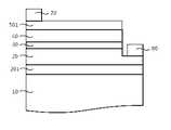
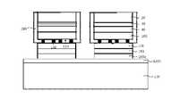
우선 먼저 도 1을 참조하면, 그룹 3족 질화물계 반도체 발광다이오드 소자는 사파이어 성장 기판(10)과 상기 성장 기판(10) 상면에 순차적으로 성장 형성된 n형 도전성의 반도체 물질로 이루어진 하부 질화물계 클래드층(20), 질화물계 활성층(30) 및 p형 도전성의 반도체 물질로 이루어진 상부 질화물계 클래드층(40)을 포함한다. 상기 하부 질화물계 클래드층(20)은 n형 In x Al y Ga 1-x-y N(0≤x, 0≤y, x+y≤1) 반도체 다층으로 이루어질 수 있으며, 상기 질화물계 활성층(30)은 다중양자우물(multi-quantum well) 구조의 다른 조성으로 구성된 그룹 3족 질화물계 In x Al y Ga 1-x-y N(0≤x, 0≤y, x+y≤1)인 반도체 다층으로 이루어질 수 있다. 또한, 상기 상부 질화물계 클래드층(40)은 p형 In x Al y Ga 1-x-y N(0≤x, 0≤y, x+y≤1) 반도체 다층으로 구성될 수 있다. 일반적으로, 상기 그룹 3족 질화물계 반도체 단결정으로 형성된 하부 질화물계 클래드층/질화물계 활성층/상부 질화물계 클래드층(20, 30, 40)은 MOCVD, MBE, HVPE, sputter, 또는 PLD 등의 장치를 이용하여 성장될 수 있다. 이때, 상기 하부 질화물계 클래드층(20)인 n형 In x Al y Ga 1-x-y N 반도체를 성장하기에 앞서, 사파이어 성장 기판(10)과의 격자정합을 향상시키기 위해, AlN 또는 GaN와 같은 버퍼층(201)을 그 사이에 형성할 수도 있다.First, referring to FIG. 1, a group III-nitride semiconductor light emitting diode device includes a lower nitride-based cladding layer made of a
상기한 바와 같이, 상기 사파이어 성장 기판(10)은 전기절연성 물질이므로, LED 소자의 두 전극을 모두 단결정 반도체 성장방향인 동일한 상면에 형성해야 하며, 이를 위해서는 상부 질화물계 클래드층(40)과 질화물계 활성층(30)의 일부 영역을 에칭(즉, 식각)하여 하부 질화물계 클래드층(20)의 일부 상면 영역을 대기에 노출시키고, 대기에 노출된 상기 하부 질화물계 클래드층(20)인 n형 In x Al y Ga 1-x-y N 반도체 상면에 n형 오믹접촉(ohmic contact interface) 전극 및 전극패드(80)를 형성한다.As described above, since the
특히, 상기 상부 질화물계 클래드층(40)은 낮은 캐리어 농도(carrier concentration) 및 작은 이동도(mobility)로 인하여 상대적으로 높은 면저항을 갖고 있기 때문에, p형 전극(70)을 형성하기에 앞서, 양질의 오믹접촉 커런트스프레딩층(501)을 형성할 수 있는 추가적인 물질이 요구된다. 이에 대하여, 미국특허 US5,563,422에서는, 그룹 3족 질화물계 반도체 발광다이오드 소자용 발광구조체의 상층부에 위치한 상부 질화물계 클래드층(40)인 p형 In x Al y Ga 1-x-y N(40) 반 도체 상면에 p형 전극(80)을 형성하기 전, 수직방향으로의 비접촉 저항이 낮은 오믹접촉 계면(ohmic contact interface)을 형성하는 오믹접촉 커런트스프레딩층(501)을 형성하기 위해 산화시킨 니켈-금(Ni-O-Au)로 구성된 물질을 제안하였다.In particular, since the upper nitride-based
상기 오믹접촉 커런트스프레딩층(501)은 상부 질화물계 클래드층(40)인 p형 In x Al y Ga 1-x-y N 반도체 상면에 위치하면서 수평방향으로의 전류 퍼짐(current spreading)을 향상시키면서도 동시에, 수직방향으로의 낮은 비접촉 저항을 갖는 오믹접촉 계면을 형성하여 효과적인 전류 주입(current injection)을 할 수 있어, 발광다이오드 소자의 전기적인 특성을 향상시킨다. 그러나 산화시킨 니켈-금으로 구성된 오믹접촉 커런트스프레딩층(501)은 열처리를 거친 후에도 평균 70%의 낮은 투과율을 보이며, 이러한 낮은 빛 투과율은 해당 발광다이오드 소자에서 생성된 빛을 외부로 방출될 때, 많은 양의 빛을 흡수하여 전체 외부 발광 효율을 감소시키게 한다.The ohmic contact
상기한 바와 같이, 오믹접촉 커런트스프레딩층(501)의 높은 빛 투과율을 통한 고휘도 발광다이오드 소자를 얻기 위한 방안으로, 최근 들어 상기 산화시킨 니켈-금(Ni-O-Au) 물질을 비롯한 각종 반투명성 금속 또는 합금으로 형성된 오믹접촉 커런트스프레딩층(501) 대신에 투과율이 평균 90% 이상인 것으로 알려진 ITO(indium tin oxide) 또는 ZnO(zinc oxide) 등의 투명 전도성 물질로 형성하는 방안이 제안되었다. 그런데, 상기한 투명 전기전도성 물질은 상부 질화물계 클래드층(40)인 p형 In x Al y Ga 1-x-y N(0≤x, 0≤y, x+y≤1) 반도체(~7.5 eV 이상)에 비해 작은 일함수(4.7~6.1eV), 그리고 p형 In x Al y Ga 1-x-y N 반도체 상면에 직 접적으로 증착하고 열처리를 포함한 후속 공정을 행한 후에 오믹접촉 계면이 아니라 비접촉 저항이 큰 쇼키접촉 계면(schottky contact interface)을 형성하고 있어, 상기한 문제점을 해결할 수 있는 새로운 투명 전도성 물질 또는 제조 공정이 필요하다.As described above, in order to obtain a high-brightness light emitting diode device through high light transmittance of the ohmic contact
상기한 ITO 또는 ZnO 등의 투명 전도성 물질이 상기 상부 질화물계 클래드층(40)인 p형 In x Al y Ga 1-x-y N(0≤x, 0≤y, x+y≤1) 반도체 상면에서의 양호한 오믹접촉 커런트스프레딩층(501)으로서 역할을 이행할 수 있도록, 최근에 Y. K. Su 등은 여러 문헌에서 상기한 투명 전기전도성 물질을 상부 질화물계 클래드층(40)인 p형 In x Al y Ga 1-x-y N (0≤x, 0≤y, x+y≤1) 반도체 상면에 직접적 증착 형성하기에 앞서, 슈퍼래티스 구조(superlattice structure)를 개재하여 오믹접촉 계면을 갖는 커런트스프레딩층(501) 형성 기술을 제안하였다.The transparent conductive material such as ITO or ZnO is formed on the upper surface of the p-type In x Al y Ga 1-xy N (0 ≦ x, 0 ≦ y, x + y ≦ 1) semiconductor of the upper nitride-based
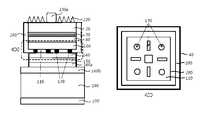
도 2에 도시된 바와 같이, 상기 슈퍼래티스 구조(superlattice structure)는 다중양자우물 구조(multi-quantum well structure)에서 우물(well, b1)과 장벽(barrier, a1)의 두층(a1, b1)이 한쌍(one pair)으로 주기적으로 반복된 점은 유사하나, 상기 다중양자우물 구조의 장벽(a1) 두께는 우물(b1) 두께에 비해서 상대적으로 두꺼운 반면에, 상기 슈퍼래티스 구조를 구성하고 있는 두층(a2, b2)은 모두 5nm 이하의 얇은 두께를 지니고 있다. 상기한 특징으로 인하여, 상기 다중양자우물 구조는 캐리어인 전자 또는 정공을 두꺼운 장벽(a1) 사이에 위치하는 우물(b1)에 가두는(confinement) 역할과는 달리, 상기 슈퍼래티스 구조는 전자 또는 정공의 흐름(transport)을 용이하게 도와주는 역할을 한다.As shown in FIG. 2, the superlattice structure includes two wells (b1) and a barrier (a1) of a well (b1) and a barrier (a1) in a multi-quantum well structure. Although the points repeated periodically in one pair are similar, the thickness of the barrier (a1) of the multi-quantum well structure is relatively thick compared to the thickness of the well (b1), while the two layers constituting the superlattice structure ( a2 and b2) both have a thin thickness of 5 nm or less. Due to the above characteristics, the multi-quantum well structure is different from the role of confining electrons or holes, which are carriers, to the well b1 located between the thick barriers a1. It helps to facilitate transport.
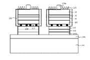
Y. K. Su 등이 제안한 슈퍼래티스 구조를 이용하여 오믹접촉 커런트스프레딩층(60)을 구비하고 있는 발광다이오드 소자를 도 3을 참조하여 설명하면, 그룹 3족 질화물계 반도체 발광다이오드 소자는 사파이어 성장 기판(10)과 상기 성장 기판(10) 상면에 형성된 n형 도전성의 반도체 물질로 이루어진 하부 질화물계 클래드층(20), 질화물계 활성층(30), p형 도전성의 반도체 물질로 이루어진 상부 질화물계 클래드층(40), 및 슈퍼래티스 구조(90)를 포함한다. 특히, 상기 슈퍼래티스 구조(90)는 상기 하부 질화물계 클래드층(20), 질화물계 활성층(30), 및 상부 질화물계 클래드층(40)과 동일한 성장 장비로 인시츄(in-situ) 상태에서 성장 형성한다. 상기 하부 질화물계 클래드층(20)은 n형 In x Al y Ga 1-x-y N(0≤x, 0≤y, x+y≤1) 반도체 다층으로 이루어질 수 있으며, 상기 질화물계 활성층(30)은 다중양자우물(multi-quantum well)구조의 다른 조성으로 구성된 그룹 3족 질화물계 In x Al y Ga 1-x-y N(0≤x, 0≤y, x+y≤1) 반도체 다층으로 이루어질 수 있다. 상기 상부 질화물계 클래드층(40)은 p형 In x Al y Ga 1-x-y N(0≤x, 0≤y, x+y≤1) 반도체 다층으로 구성될 수 있다. 또한, 상기 슈퍼래티스 구조(90)는 다른 조성(composition)으로 구성된 그룹 3족 질화물계 In x Al y Ga 1-x-y N(0≤x, 0≤y, x+y≤1) 반도체 또는 다른 도판트(dopant)를 갖는 그룹 3족 질화물계 In x Al y Ga 1-x-y N(0≤x, 0≤y, x+y≤1) 반도체 다층으로 이루어질 수 있다.Referring to FIG. 3, a light emitting diode device having an ohmic contact current spreading
상기 슈퍼래티스 구조(90)를 구성하고 있는 조성(composition) 및 도판트(dopant) 종류에 따라 상부 질화물계 클래드층(40)인 p형 In x Al y Ga 1-x-y N (0≤x, 0≤y, x+y≤1) 반도체의 도판트 활성화 에너지를 낮추어 유효정공농도(net effective hole concentration)를 증가시키거나, 또는 에너지 밴드갭 조절(band-gap engineering)을 통해서 양자역학적 터널링 전도(quantum-mechanical tunneling transport) 현상을 통해서 오믹접촉 계면(ohmic contact interface)을 형성하는 것으로 알려져 있다.P-type In x Al y Ga 1-xy N (0 ≦ x, 0), which is the upper nitride-based
일반적으로, 상기 그룹 3족 질화물계 반도체 단결정으로 형성된 하부 질화물계 클래드층/질화물계 활성층/상부 질화물계 클래드층/슈퍼래티스 구조(20, 30, 40, 90)는 MOCVD, MBE, HVPE, 또는 sputter, 또는 PLD 등의 장치를 이용하여 성장될 수 있다. 이때, 상기 하부 질화물계 클래드층(20)의 n형 In x Al y Ga 1-x-y N 반도체를 성장하기에 앞서, 사파이어 성장 기판(10)과의 격자정합을 향상시키기 위해, AlN 또는 GaN와 같은 버퍼층(201)을 그 사이에 형성할 수도 있다.In general, the lower nitride-based cladding layer / nitride-based active layer / the upper nitride-based cladding layer /
그렇지만, 상기 상부 질화물계 클래드층(40) 상면에 위치하는 투명 전기전도성 물질로 구성된 오믹접촉 커런트스프레딩층(501 또는 60)에 이용되는 재료는 투과율과 전기전도율이 절충(trade-off) 관계에 있다. 즉, 투과율을 높이기 위해 상기 오믹접촉 커런트스프레딩층(501 또는 60) 두께를 작게 하면, 반대로 전기전도율이 저하해 버려, 그룹 3족 질화물계 반도체 발광다이오드 소자의 시리즈 저항(series resistance) 상승과 이로 인해서 소자 신뢰성 저하의 원인으로 된다는 문제가 있었다.However, the material used for the ohmic contact
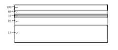
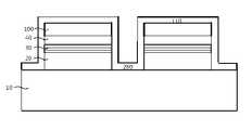
그래서, 투명 전기전도성 물질로 구성된 오믹접촉 커런트스프레딩층을 이용하지 않는 방법으로서, 광학적으로 투명한 성장 기판인 경우에 발광다이오드 소자용 발광구조체의 상부 질화물계 클래드층 상면에 반사율이 높은 전기전도성 물질로 구성된 오믹접촉 커런트스프레딩층(502)을 형성하는 구조를 생각할 수 있다. 이것이 도 4에 나타낸 플립칩 구조(flip-chip structure)의 그룹 3족 질화물계 반도체 발광다이오드 소자의 단면도이다.Thus, a method of not using an ohmic contact current spreading layer composed of a transparent electroconductive material, and in the case of an optically transparent growth substrate, an electrically conductive material having high reflectance on the upper nitride-based cladding layer of the light emitting structure for a light emitting diode device A structure for forming the configured ohmic contact
도시한 바와 같이, 플립칩 구조의 그룹 3족 질화물계 반도체 발광다이오드 소자는 광학적으로 투명한 사파이어 성장 기판(10)과 상기 성장 기판(10) 상면에 순차적으로 성장 형성된 n형 도전성의 반도체 물질로 이루어진 하부 질화물계 클래드층(20), 질화물계 활성층(30) 및 p형 도전성의 반도체 물질로 이루어진 상부 질화물계 클래드층(40)을 포함한다. 상기 상부 질화물계 클래드층(40) 상면에 높은 반사율을 갖는 전기전도성 물질로 구성된 오믹접촉 커런트스프레딩층(502)을 형성하고, 발광다이오드 소자용 발광구조체인 질화물계 활성층(30)에서 생성된 빛을 높은 반사율을 갖는 오믹접촉 커런트스프레딩층(502)을 이용하여 반대방향으로 반사시키고, 광학적으로 투명한 성장 기판(10) 쪽으로 발광시키는 것이다.As shown, the group III nitride semiconductor light emitting diode device of the flip chip structure is formed of an optically transparent
일반적으로, 그룹 3족 질화물계 반도체를 이용하여 널리 실용화되어 있는 발광다이오드 소자는 질화물계 활성층(30)에 InGaN, AlGaN 등을 이용하여 자외선~청색~녹색으로 발생하는 것이고, 사용되고 있는 성장 기판(10)인 사파이어(sapphire)이다. 상기 성장 기판(10)으로 사용되는 사파이어는 상당히 넓은 밴드갭을 갖는 물질이기 때문에 그룹 3족 질화물계 반도체 발광다이오드 소자에서 발광하는 빛에 대해 모두 투명하다. 그 때문에, 특히 그룹 3족 질화물계 반도체 발광다이오드 소자에서는 상기한 플립칩 구조는 대단히 유효한 수단이라고 말할 수 있지만, p형 도전성을 갖는 상부 질화물계 클래드층(40)과 오믹접촉 계면을 형성하고 높은 반사율을 갖는 물질은 한정적이다. 일반적으로 높은 반사율을 갖고 있는 금속 물질은 은(Ag), 알루미늄(Al), 로듐(Rh)이 대표적이다. 상기 은(Ag)과 로듐(Rh), 그리고 이들과 관련된 합금(alloy)은 상기 상부 질화물계 클래드층(40)과 양호한 오믹접촉 계면을 나타내고 있지만, 이들 물질의 금속 또는 합금은 발광다이오드 소자용 발광구조체 내부로 물질이동인 확산 현상이 발생하고, 발광다이오드 소자의 동작전압의 상승 및 신뢰성을 저하시킨다는 문제가 있었다. 또한, 열적으로 불안정한 은(Ag)과 로듐(Rh), 그리고 이들과 관련된 합금(alloy)은 400nm 이하의 단파장 영역인 자외선(ultraviolet)에 대해 낮은 반사율을 나타내어, 자외선용 발광다이오드 소자의 오믹접촉 커런트스프레딩층(502) 물질로는 바람직하지 않다. 한편, 상기 알루미늄(Al) 및 이와 관련된 합금은 자외선 영역까지 높은 반사율을 갖고 있지만, p형 도전성을 갖는 상부 질화물계 클래드층(40)과 바람직한 오믹접촉 계면이 아닌 쇼키접촉 계면을 형성하기 때문에 사용할 수가 없는 상태이다. 이 때문에, 플립칩 구조의 그룹 3족 질화물계 반도체 발광다이오드 소자를 실현하기 위해서는 p형 도전성을 갖는 상부 질화물계 클래드층(40) 상면에서 오믹접촉 계면과 높은 반사율을 갖는 오믹접촉 커런트스프레딩층(502)을 형성할 수 있는 물질 또는 구조를 개발할 필요가 있다.In general, a light emitting diode device that is widely used using a group III nitride semiconductor is generated using ultraviolet light, blue light, or green light using InGaN, AlGaN, etc. in the nitride
한편, 상기의 일반적인 구조 및 플립칩 구조의 그룹 3족 질화물계 반도체 발광다이오드 소자는 수평구조로서, 낮은 열전도 및 전기절연성인 사파이어 성장 기판(10)에 제조되기 때문에, 발광다이오드 소자 구동 시 필연적으로 발생하는 다량의 열을 원활히 방출하는데 어려움이 있어 소자의 전체적인 특성을 저하시키는 문 제점이 있다.On the other hand, the group III-nitride semiconductor light emitting diode device of the general structure and the flip chip structure is produced in the
또한, 도시 및 설명한 바와 같이, 두 오믹접촉 전극 및 전극패드 형성을 위해서는 질화물계 활성층(40)의 일부 영역을 제거해야 하며, 이에 따라 발광면적이 감소하여 양질의 발광다이오드소자를 실현하기 어렵고, 동일한 사이즈 웨이퍼에서 칩의 개수가 줄어들어 단가 경쟁력에서 뒤처지게 된다.In addition, as shown and described, in order to form two ohmic contact electrodes and electrode pads, a part of the nitride-based
또한, 웨이퍼 상부에 발광다이오드 소자의 제조 공정이 완료된 후, 단일화된 발광다이오드 소자로 분리하기위해 하는 래핑(lapping), 폴리싱(polishing), 스크라이빙(scribing), 소잉(sawing), 및 브레이킹(breaking) 등의 기계적인 공정 시에 사파이어 성장 기판(10)과 그룹 3족 질화물계 반도체의 벽개면(cleavage plane)의 불일치로 인하여 불량률이 높아 전체적인 제품수율이 떨어지는 단점도 갖고 있다.In addition, after the manufacturing process of the light emitting diode device on the wafer is completed, lapping, polishing, scribing, sawing, and braking to separate into a single light emitting diode device Due to the mismatch between the
최근 들어, 상기 수평구조의 그룹 3족 질화물계 반도체 발광다이오드 소자의 문제점을 해결하기 위한 것으로, 성장 기판(10)을 제거하여 두 오믹접촉 전극 및 전극패드가 발광다이오드 소자의 상/하부에 대향되게 위치시켜, 외부에서 인가된 전류가 한 방향으로 흐르게 되어 발광효율이 향상된 수직구조의 그룹 3족 질화물계 반도체 발광다이오드 소자가 많은 문헌들(미국특허, US 6,071,795, US 6,335,263, US 20060189098)에서 개시되고 있다.Recently, in order to solve the problem of the group III-nitride-based semiconductor LED device having a horizontal structure, the
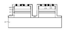
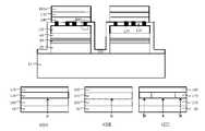
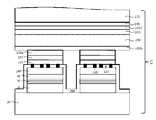
도 47은 종래 기술의 일예로서, 수직구조의 그룹 3족 질화물계 반도체 발광다이오드 소자의 일반적인 제조 공정을 보인 단면도이다. 도 47에 도시된 바와 같이, 일반적인 수직구조의 발광다이오드 소자 제조 방법은 사파이어 성장 기판(10) 위에 MOCVD 또는 MBE 성장 장비를 이용하여 발광다이오드 소자용 발광구조체를 형 성시킨 후에 상기 발광다이오드 소자용 발광구조체의 최상층부에 존재하는 상부 질화물계 클래드층(50) 상부에 반사성 p형 오믹접촉 전극구조체(90)를 형성시킨 다음, 상기 성장 기판 웨이퍼와 별도로 준비된 지지 기판 웨이퍼를 300℃ 미만의 온도에서 솔더링 웨이퍼 결합(solder bonding)한 다음, 사파이어 성장 기판을 제거하여 수직구조의 발광다이오드 소자를 제조하는 것이다.FIG. 47 is a sectional view showing a general manufacturing process of a group III-nitride semiconductor light emitting diode device having a vertical structure as an example of the prior art. As illustrated in FIG. 47, in the method of manufacturing a light emitting diode device having a general vertical structure, the light emitting diode light emitting device is formed on the
도 47을 참조하여 더욱 상세하게 설명하면, 먼저 사파이어 기판(10)의 상부에 MOCVD 성장 장비를 이용하여, 언도프(undope)된 GaN 또는 InGaN 버퍼층(20), 하부 질화물계 클래드층(30), InGaN 및 GaN으로 형성된 질화물계 활성층(40), 상부 질화물계 클래드층(50)을 순차적으로 성장한 발광다이오드 소자용 발광구조체를 형성한 다음(도 47A), 상기 상부 질화물계 클래드층(50)의 상부에 반사성 p형 오믹접촉 전극구조체(90), 및 솔더링 반응 방지층(100)을 순차적으로 형성하여 성장 기판 웨이퍼(growth substrate wafer)를 준비한다(도 47B). 그런 다음, 도 47C에 나타난 바와 같이, 전기전도성인 지지 기판(110)의 상부와 하부 각각에 두 오믹접촉 전극(120, 130)을 형성하고, 상기 발광다이오드 소자용 발광구조체을 결합시키기 위한 솔더링 물질(140)을 증착하여 지지 기판 웨이퍼를 준비한다. 그런 후에, 제조된 성장 기판 웨이퍼의솔더링 물질 확산방지층(100)과 지기기판 웨이퍼의 솔더링 물질(140)을 도 47D에 도시된 바와 같이 맞닿게 하여 솔더링 웨이퍼 결합한다. 그 후, 상기 단일화된 다수개의 발광다이오드 소자들이 제조된 성장 기판 웨이퍼의 후면인 사파이어 성장 기판(10) 후면에 강한 에너지를 갖는 레이저를 조사하여 사파이어 성장 기판(10)을 다수개의 발광다이오드 소자들로부터 분리시키고(레이저 리 프트오프;LLO), 레이저에 의해 손상된 언도프(undope)된 GaN 또는 InGaN 버퍼층(20)은 건식식각 공정을 이용하여 하부 질화물계 클래드층(30)이 노출될 때까지 전면으로 식각하고(도 47E), 상기 다수개의 발광다이오드 소자들에 해당하는 하부 질화물계 클래드층(30)의 상부에 n형 오믹접촉 전극구조체(80)를 형성한다(도 47F). 마지막으로, 상기 다수개의 발광다이오드 소자들과 전기전도성 지지 기판(110)에 래핑(lapping), 폴리싱(polishing), 스크라이빙(scribing), 소잉(sawing), 및 브레이킹(breaking) 등의 기계적인 절단공정을 수행하여 단일화된 발광다이오드 소자로 분리한다(도 47G).Referring to FIG. 47, the undoped GaN or
하지만, 상기한 종래 수직구조의 발광다이오드 소자 제조 공정 기술은 하기와 같은 여러 문제점이 있어, 단일화된 수직구조의 발광다이오드 소자를 대량으로 안전하게 확보하기가 어렵다. 즉, 상기 솔더링 웨이퍼 결합을 낮은 온도 범위 내에서 수행하기 때문에, 그 이후에 행해지는 공정에서는 솔더링 웨이퍼 결합 온도보다 높은 고온 공정을 행할 수 없어, 열적으로 안정한 발광다이오드 소자 구현이 어렵다. 더 나아가서, 열팽창계수와 격자상수가 다른 이종 웨이퍼(dissimilar wafer) 사이에 결합을 하기 때문에, 결합 시에 열적 응력을 발생시켜 발광다이오드 소자의 신뢰성에 치명적인 영향을 미친다.However, the conventional vertical light emitting diode manufacturing process technology has a number of problems as described below, it is difficult to secure a large amount of a secure light emitting diode device of a single vertical structure. That is, since the soldering wafer bonding is performed within a low temperature range, a subsequent high temperature process cannot be performed at a higher temperature than the soldering wafer bonding temperature, and thus it is difficult to implement a thermally stable light emitting diode device. Furthermore, since the bonding is performed between dissimilar wafers having different thermal expansion coefficients and lattice constants, thermal stress is generated during the bonding, which has a critical effect on the reliability of the light emitting diode device.
더 최근 들어, 상기한 솔더링 웨이퍼 결합에 의해 제조되는 수직구조의 그룹 3족 질화물계 반도체 발광다이오드 소자에서 발생하는 문제점을 해결하기 위해서, 솔더링 웨이퍼 결합에 의해서 형성된 전기전도성 지지 기판 대신에 Cu, Ni 등의 금속 후막을 전기도금(electroplating) 공정에 의해 상기 반사성 p형 오믹접촉 전극 구조체(90) 상부에 형성시키는 기술이 개발되어 부분적으로 제품 생산에 이용되고 있다.More recently, in order to solve the problems occurring in the vertical group III-nitride semiconductor light emitting diode device manufactured by the soldering wafer bonding, Cu, Ni, and the like instead of the electroconductive supporting substrate formed by the soldering wafer bonding. A technique for forming a thick metal film on the reflective p-type ohmic
그러나, 상기 전기도금 공정과 접목되어 제조된 수직구조의 발광다이오드 제조 공정에서 발생하는 후속 공정들, 즉 고온 열처리, 래핑, 폴리싱, 스크라이빙, 소잉(sawing), 및 브레이킹 등의 기계적인 절단공정이 행해질 때 소자의 성능 저하 및 불량 발생 등의 문제점이 여전히 해결해야 할 과제로 남아 있다.However, subsequent processes arising in the vertical structured light emitting diode manufacturing process combined with the electroplating process, ie, mechanical cutting processes such as high temperature heat treatment, lapping, polishing, scribing, sawing, and braking. When this is done, problems such as deterioration of the device and occurrence of defects still remain problems to be solved.
본 발명은 상기 지적된 문제들을 인식하여 이루어진 것으로, 성장 기판(growth substrate) 상면에 화학식 In x Al y Ga 1-x-y N(0≤x, 0≤y, x+y≤1)으로 표기되는 그룹 3족 질화물계 반도체 발광다이오드 소자용 발광구조체와, 투명성 커런트인젝션층, 제1 패시베이션층, 도전선막체, 및 반사성 커런트스프레딩층으로 구성된 p형 전극구조체를 구비한 성장 기판 웨이퍼(growth substrate wafer)와 본 발명자에 의해 개발된 샌드위치 구조의 웨이퍼 결합(sandwich-structured wafer bonding) 공정을 접목시켜 수직구조의 발광다이오드 소자 및 제조 방법에 관한 것이다.The present invention has been made in recognition of the above-mentioned problems, and is a group represented by the formula In x Al y Ga 1-xy N (0 ≦ x, 0 ≦ y, x + y ≦ 1) on the growth substrate. A growth substrate wafer having a p-type electrode structure composed of a light emitting structure for a group III nitride semiconductor light emitting diode device, a transparent current injection layer, a first passivation layer, a conductive line film body, and a reflective current spreading layer. And a sandwich-structured wafer bonding process developed by the present inventors, and a light emitting diode device having a vertical structure and a manufacturing method thereof.
상세하게는, 성장 기판 상층부에 p형 전극구조체를 포함한 그룹 3족 질화물계 반도체 발광다이오드 소자용 발광구조체가 준비된 성장 기판 웨이퍼(growth substrate wafer), 히트씽크 지지대인 이종 기판 웨이퍼(dissimilar support substrate), 및 임시 기판 웨이퍼(temporary substrate wafer)를 샌드위치 구조로 웨이퍼 결합을 수행한 다음, 기판 분리(lift-off) 공정을 통해 상기 성장 기판 및 임시 기판을 각각 제거하여 수직구조의 그룹 3족 질화물계 반도체 발광다이오드 소자 및 그 제조 방법을 제공하고자 한다.Specifically, a growth substrate wafer having a light emitting structure for a group III nitride semiconductor light emitting diode device including a p-type electrode structure in an upper portion of the growth substrate, a dissimilar support substrate as a heatsink support, And performing wafer bonding on a temporary substrate wafer in a sandwich structure, and then removing the growth substrate and the temporary substrate through a substrate lift-off process to emit light of a group III-nitride semiconductor having a vertical structure. SUMMARY To provide a diode device and a method of manufacturing the same.
상기의 목적을 달성하기 위해,In order to achieve the above object,
부분 n형 전극구조체; 상기 부분 n형 전극구조체 하면에 하부 질화물계 클래 드층, 질화물계 활성층, 및 상부 질화물계 클래드층으로 구성된 발광다이오드 소자용 발광구조체; 상기 발광구조체 하면에 형성된 투명성 커런트인젝션층, 제1 패시베이션층, 도전선막체, 및 반사성 커런트스프레딩층으로 구성된 p형 전극구조체; 상기 p형 전극구조체 하면에 형성된 히트씽크 지지대; 상기 히트씽크 지지대 하면에 형성된 p형 오믹접촉 전극패드;를 포함하는 수직구조의 그룹 3족 질화물계 반도체 발광다이오드 소자를 제공한다.Partial n-type electrode structures; A light emitting structure for a light emitting diode device comprising a lower nitride based cladding layer, a nitride based active layer, and an upper nitride based cladding layer on a lower surface of the partial n-type electrode structure; A p-type electrode structure including a transparent current injection layer, a first passivation layer, a conductive line film body, and a reflective current spreading layer formed on a lower surface of the light emitting structure; A heat sink support formed on a bottom surface of the p-type electrode structure; A p-type ohmic contact electrode pad formed on a bottom surface of the heat sink supporter is provided.
상기 부분 n형 전극구조체(partialn-type electrode system)는 상기 하부 질화물계 클래드층 상면 일부 영역에 소정의 형상 및 치수를 갖고 있으며, 600nm 이하의 파장대역에서 50% 이상의 반사율을 갖는 반사성 오믹접촉 전극(reflective ohmic contacting electrode) 및 반사성 전극패드(reflective electrode pad)로 구성한다.The partial n-type electrode structure (partialn -type electrode system) is a reflective ohmic contact electrode having a reflectance of 50% or more, and has a predetermined shape and dimensions of the upper surface on a portion of the lower nitride-based cladding layer, at the wavelength band of 600nm or less It consists of a reflective ohmic contacting electrode and a reflective electrode pad.
또 다른 한편으로, 상기 부분 n형 전극구조체(partialn-type electrode system)는 상기 하부 질화물계 클래드층 상면 일부 영역에 소정의 형상 및 치수를 갖고 있으며, 600nm 이하의 파장대역에서 50% 이상의 반사율을 갖는 반사성 쇼키접촉 전극(reflective schottky contacting electrode) 및 반사성 전극패드(reflective electrode pad)로 구성한다.On the other hand, the partial n-type electrode structure (partialn- type electrode system) has a predetermined shape and dimensions in a portion of the upper surface of the lower nitride-based cladding layer, and has a reflectance of 50% or more in the wavelength band of 600nm or less And a reflective schottky contacting electrode and a reflective electrode pad.
상기 투명성 커런트인젝션층(transparent current inection layer)은 상기 상부 질화물계 클래드층과 오믹접촉 계면(ohmic contacting interface)을 형성하여 수직방향으로의 용이한 전류 주입(current injecting)하는 역할을 한다.The transparent current injection layer forms an ohmic contacting interface with the upper nitride-based cladding layer to facilitate easy current injecting in the vertical direction.
상기 투명성 커런트인젝션층은 상기 발광다이오드 소자용 발광구조체 상면에 600nm 이하의 파장대역에서 70% 이상의 투과율을 갖는 전기전도성 물질로 구성된 단층막 또는 다층막이다.The transparent current injection layer is a single layer film or a multilayer film made of an electrically conductive material having a transmittance of 70% or more in a wavelength band of 600 nm or less on an upper surface of the light emitting structure for a light emitting diode device.
상기 제1 패시베이션층(first passivation layer)은 발광다이오드 소자용 발광구조체의 상면을 보호하는 동시에, 상기 반사성 커런트스프레딩층을 구성하는 물질이 상기 투명성 커런트인젝션층 및 발광구조체 내부로의 확산 이동을 방지(diffusion barrier)하는 역할을 한다.The first passivation layer protects an upper surface of the light emitting structure for the light emitting diode device, and prevents the material constituting the reflective current spreading layer from diffusing into the transparent current injection layer and the light emitting structure. (diffusion barrier)
상기 제1 패시베이션층은 전기적으로 절연성이면서 600nm 이하의 파장대역에서 70% 이상의 투과율을 갖는 물질로 구성된 단층막 또는 다층막이다.The first passivation layer is a single layer film or a multilayer film made of a material which is electrically insulating and has a transmittance of 70% or more in a wavelength band of 600 nm or less.
상기 제1 패시베이션층은 전체 영역의 50% 이하 영역이 비아홀(via-hole) 형태로 패터닝된 다음, 상기 제1 패시베이션층 상/하면에 위치한 상기 투명성 커런트인젝션층과 상기 반사성 커런트스프레딩층을 전기적으로 연결하는 도전선막체로 충진(filling)되어 있다.In the first passivation layer, 50% or less of the entire area is patterned in the form of via-holes, and then the transparent current injection layer and the reflective current spreading layer are disposed on the upper and lower surfaces of the first passivation layer. It is filled with a conductive wire to connect to.
또 다른 한편으로, 상기 투명성 커런트인젝션층과 제1 패시베이션층은 전체 영역의 50% 이하 영역이 비아홀(via-hole) 형태로 패터닝된 다음, 상기 제1 패시베이션층 상/하면에 위치한 상기 투명성 커런트인젝션층과 상기 반사성 커런트스프레딩층을 전기적으로 연결하는 도전선막체로 충진(filling)함과 동시에, 상기 도전선막체는 상부 질화물계 클래드층과 쇼키접촉 계면(schottky contacting interface) 또는 오믹접촉 계면(ohmic contacting interface)을 형성하면서 직접적으로 접촉하고 있다.On the other hand, the transparent current injection layer and the first passivation layer is less than 50% of the entire area is patterned in the form of via-holes (via-hole), then the transparent current injection located on the upper / lower surface of the first passivation layer The conductive wire film is filled with a conductive wire film electrically connecting the layer and the reflective current spreading layer, and the conductive wire film has a schottky contacting interface or an ohmic contacting interface with the upper nitride cladding layer. direct contact, forming an interface).
상기 반사성 커런트스프레딩층(reflective current spreading layer)은 상기 제1 패시베이션층 상면에서 수평방향으로의 전류 퍼짐과 도전선막체를 통해 상기 상부 질화물계 클래드층 또는 투명성 커런트인젝션층에 전류를 전도하는 동시에, 상기 발광다이오드 소자용 발광구조체에서 생성된 빛을 반대방향으로 반사시키는 역할을 한다.The reflective current spreading layer spreads current in the horizontal direction on the upper surface of the first passivation layer and conducts current to the upper nitride based cladding layer or transparent current injection layer through a conductive wire film. It serves to reflect the light generated in the light emitting structure for the light emitting diode device in the opposite direction.
상기 반사성 커런트스프레딩층은 상기 제1 패시베이션층 상면에 600nm 이하의 파장대역에서 80% 이상의 반사율을 갖는 전기전도성 물질로 구성된 단층막 또는 다층막이다.The reflective current spreading layer is a single layer film or a multilayer film made of an electrically conductive material having a reflectivity of 80% or more in a wavelength band of 600 nm or less on an upper surface of the first passivation layer.
상기 히트씽크 지지대(heat-sink support)는 전기 또는 열적으로 우수한 전도율을 갖는 것이 바람직하다. 이 경우, 상기 히트씽크 지지대는 Si, GaAs, Ge, SiGe, AlN, GaN, AlGaN, SiC, AlSiC 등의 웨이퍼(wafer)와 Ni, Cu, Nb, CuW, NiW, NiCu 등의 플레이트(plate) 또는 호일(foil)을 우선적으로 선택한다.The heat-sink support preferably has good electrical or thermal conductivity. In this case, the heat sink support may be a wafer such as Si, GaAs, Ge, SiGe, AlN, GaN, AlGaN, SiC, AlSiC, or a plate such as Ni, Cu, Nb, CuW, NiW, NiCu, or the like. The foil is selected first.
본 발명의 수직구조의 그룹 3족 질화물계 반도체 발광다이오드 소자에서, p형 전극구조체는 수직방향으로의 전류 집중 방지와 빛에 대한 반사체 역할 이외에도, 물질의 확산 방지, 물질간의 결합 및 결합성 향상, 또는 물질의 산화 방지 역할을 수행할 수 있는 별도의 박막층을 포함하는 것이 바람직하다.In the group III-nitride semiconductor light-emitting diode device of the vertical structure of the present invention, the p-type electrode structure, in addition to preventing current concentration in the vertical direction and acting as a reflector for light, prevents diffusion of materials, improves bonding and bonding between materials, Or it is preferable to include a separate thin film layer that can perform the role of preventing the oxidation of the material.
또 다른 한편, 상기 그룹 3족 질화물계 반도체 발광다이오드 소자용 발광구조체는 상기 투명성 커런트인젝션층을 형성하기에 앞서, 널리 공지된 5nm 이하의 두께를 갖는 n형 도전성의 InGaN, GaN, AlInN, AlN, InN, AlGaN, AlInGaN, SiC, SiCN, MgN, ZnN 단층, 5nm 이하의 두께를 갖는 p형 도전성의 InGaN, GaN, AlInN, AlN, InN, AlGaN, AlInGaN 단층, 다른 도판트(dopant)와 조성(composition) 원소를 갖는 그룹 2족, 3족, 또는 4족 원소의 질화물(nitride) 또는 탄소질화물(carbon nitride)로 구성된 슈퍼래티스 구조(superlattice)도 포함할 수 있다.On the other hand, the light emitting structure for the group III-nitride semiconductor light emitting diode device is a n-type conductive InGaN, GaN, AlInN, AlN, having a thickness of 5 nm or less well known prior to forming the transparent current injection layer InN, AlGaN, AlInGaN, SiC, SiCN, MgN, ZnN single layer, p type conductive InGaN, GaN, AlInN, AlN, InN, AlGaN, AlInGaN single layer, other dopants and compositions It may also include a superlattice consisting of a nitride or carbon nitride of the
상기의 또 다른 목적을 달성하기 위해,In order to achieve the above another object,
전면 n형 전극구조체; 상기 전면 n형 전극구조체 하면에 하부 질화물계 클래드층, 질화물계 활성층, 및 상부 질화물계 클래드층으로 구성된 발광다이오드 소자용 발광구조체; 상기 발광구조체 하면에 형성된 투명성 커런트인젝션층, 제1 패시베이션층, 도전선막체, 및 반사성 커런트스프레딩층으로 구성된 p형 전극구조체; 상기 p형 전극구조체 하면에 형성된 히트씽크 지지대; 상기 히트씽크 지지대 하면에 형성된 p형 오믹접촉 전극패드;를 포함하는 수직구조의 그룹 3족 질화물계 반도체 발광다이오드 소자를 제공한다.Front n-type electrode structure; A light emitting structure for a light emitting diode device comprising a lower nitride based cladding layer, a nitride based active layer, and an upper nitride based cladding layer on a lower surface of the front n-type electrode structure; A p-type electrode structure including a transparent current injection layer, a first passivation layer, a conductive line film body, and a reflective current spreading layer formed on a lower surface of the light emitting structure; A heat sink support formed on a bottom surface of the p-type electrode structure; A p-type ohmic contact electrode pad formed on a bottom surface of the heat sink supporter is provided.
상기 전면 n형 전극구조체(fulln-type electrode system)는 상기 하부 질화물계 클래드층 상면의 전체 영역과 오믹접촉 계면을 형성하고 600nm 이하의 파장대역에서 70% 이상의 투과율을 갖는 투명성 오믹접촉 전극(transparent ohmic contacting electrode)과 상기 투명성 오믹접촉 전극 상면에 형성하고 600nm 이하의 파장대역에서 50% 이상의 반사율을 갖는 반사성 오믹접촉 전극패드(reflective ohmic contacting electrode pad)로 구성한다.The front n-type electrode structure (fulln -type electrode system) is transparent ohmic contact electrode (transparent with a transmittance of 70% or more in the wavelength band below and forming the entire area of the upper surface of the bottom nitride-based cladding layer and the ohmic contact interface 600nm Ohmic contacting electrode and a transparent ohmic contact electrode formed on the upper surface and comprises a reflective ohmic contacting electrode pad (reflective ohmic contacting electrode pad) having a reflectance of 50% or more in the wavelength band of 600nm or less.
또 다른 한편으로, 상기 전면 n형 전극구조체(fulln-type electrode system)는 상기 하부 질화물계 클래드층 상면의 전체 영역과 오믹접촉 계면을 형성하고 600nm 이하의 파장대역에서 70% 이상의 투과율을 갖는 투명성 오믹접촉 전극(transparent ohmic contacting electrode)과 상기 투명성 오믹접촉 전극 상면에 형성하고 600nm 이하의 파장대역에서 50% 이상의 반사율을 갖는 반사성 쇼키접촉 전극패드(reflective schottky contacting electrode pad)로 구성한다.Further, on the other hand, the front-side n-type electrode structure (fulln -type electrode system) is transparent with a transmittance of 70% or more in the wavelength band below and forming the entire area of the upper surface of the bottom nitride-based cladding layer and the ohmic contact interface 600nm A transparent ohmic contacting electrode and a reflective schottky contacting electrode pad are formed on the transparent ohmic contact electrode and have a reflectivity of 50% or more in a wavelength band of 600 nm or less.
상기 투명성 커런트인젝션층(transparent current inection layer)은 상기 상부 질화물계 클래드층과 오믹접촉 계면(ohmic contacting interface)을 형성하여 수직방향으로의 용이한 전류 주입(current injecting)하는 역할을 한다.The transparent current injection layer forms an ohmic contacting interface with the upper nitride-based cladding layer to facilitate easy current injecting in the vertical direction.
상기 투명성 커런트인젝션층은 상기 발광다이오드 소자용 발광구조체 상면에 600nm 이하의 파장대역에서 70% 이상의 투과율을 갖는 전기전도성 물질로 구성된 단층막 또는 다층막이다.The transparent current injection layer is a single layer film or a multilayer film made of an electrically conductive material having a transmittance of 70% or more in a wavelength band of 600 nm or less on an upper surface of the light emitting structure for a light emitting diode device.
상기 제1 패시베이션층(first passivation layer)은 발광다이오드 소자용 발광구조체의 상면을 보호하는 동시에, 상기 반사성 커런트스프레딩층을 구성하는 물질이 상기 투명성 커런트인젝션층 및 발광구조체 내부로의 확산 이동을 방지(diffusion barrier)하는 역할을 한다.The first passivation layer protects an upper surface of the light emitting structure for the light emitting diode device, and prevents the material constituting the reflective current spreading layer from diffusing into the transparent current injection layer and the light emitting structure. (diffusion barrier)
상기 제1 패시베이션층은 전기적으로 절연성이면서 600nm 이하의 파장대역에서 70% 이상의 투과율을 갖는 물질로 구성된 단층막 또는 다층막이다.The first passivation layer is a single layer film or a multilayer film made of a material which is electrically insulating and has a transmittance of 70% or more in a wavelength band of 600 nm or less.
상기 제1 패시베이션층은 전체 영역의 50% 이하 영역이 비아홀(via-hole) 형태로 패터닝된 다음, 상기 제1 패시베이션층 상/하면에 위치한 상기 투명성 커런트인젝션층과 상기 반사성 커런트스프레딩층을 전기적으로 연결하는 도전선막체로 충진(filling)되어 있다.In the first passivation layer, 50% or less of the entire area is patterned in the form of via-holes, and then the transparent current injection layer and the reflective current spreading layer are disposed on the upper and lower surfaces of the first passivation layer. It is filled with a conductive wire to connect to.
또 다른 한편으로, 상기 투명성 커런트인젝션층과 제1 패시베이션층은 전체 영역의 50% 이하 영역이 비아홀(via-hole) 형태로 패터닝된 다음, 상기 제1 패시베 이션층 상/하면에 위치한 상기 투명성 커런트인젝션층과 상기 반사성 커런트스프레딩층을 전기적으로 연결하는 도전선막체로 충진(filling)함과 동시에, 상기 도전선막체는 상부 질화물계 클래드층과 쇼키접촉 계면(schottky contacting interface) 또는 오믹접촉 계면(ohmic contacting interface)을 형성하면서 직접적으로 접촉하고 있다.On the other hand, the transparency current injection layer and the first passivation layer is a region in which 50% or less of the entire area is patterned in the form of via-holes (via-hole), and then the transparency located on the upper and lower surfaces of the first passivation layer While filling the conductive injection layer and the reflective current spreading layer electrically connecting the current injection layer and the conductive wire layer, the conductive wire layer has a schottky contact interface or an ohmic contact interface with the upper nitride-based cladding layer. They are in direct contact, forming an ohmic contacting interface.
상기 반사성 커런트스프레딩층(reflective current spreading layer)은 상기 제1 패시베이션층 상면에서 수평방향으로의 전류 퍼짐과 도전선막체를 통해 상기 상부 질화물계 클래드층 또는 투명성 커런트인젝션층에 전류를 전도하는 동시에, 상기 발광다이오드 소자용 발광구조체에서 생성된 빛을 반대방향으로 반사시키는 역할을 한다.The reflective current spreading layer spreads current in the horizontal direction on the upper surface of the first passivation layer and conducts current to the upper nitride based cladding layer or transparent current injection layer through a conductive wire film. It serves to reflect the light generated in the light emitting structure for the light emitting diode device in the opposite direction.
상기 반사성 커런트스프레딩층은 상기 제1 패시베이션층 상면에 600nm 이하의 파장대역에서 80% 이상의 반사율을 갖는 전기전도성 물질로 구성된 단층막 또는 다층막이다.The reflective current spreading layer is a single layer film or a multilayer film made of an electrically conductive material having a reflectivity of 80% or more in a wavelength band of 600 nm or less on an upper surface of the first passivation layer.
상기 히트씽크 지지대(heat-sink support)는 전기 또는 열적으로 우수한 전도율을 갖는 것이 바람직하다. 이 경우, 상기 히트씽크 지지대는 Si, GaAs, Ge, SiGe, AlN, GaN, AlGaN, SiC, AlSiC 등의 웨이퍼(wafer)와 Ni, Cu, Nb, CuW, NiW, NiCu 등의 플레이트(plate) 또는 호일(foil)을 우선적으로 선택한다.The heat-sink support preferably has good electrical or thermal conductivity. In this case, the heat sink support may be a wafer such as Si, GaAs, Ge, SiGe, AlN, GaN, AlGaN, SiC, AlSiC, or a plate such as Ni, Cu, Nb, CuW, NiW, NiCu, or the like. The foil is selected first.
본 발명의 수직구조의 그룹 3족 질화물계 반도체 발광다이오드 소자에서, p형 전극구조체는 수직방향으로의 전류 집중 방지(current blocking)와 빛에 대한 반사체(reflecting) 역할 이외에도, 물질의 확산 방지(diffusion barrier), 물질간 의 결합 및 결합성 향상, 또는 물질의 산화 방지 역할을 수행할 수 있는 별도의 박막층을 포함하는 것이 바람직하다.In the group III-nitride-based semiconductor light emitting diode device of the vertical structure of the present invention, the p-type electrode structure prevents diffusion of materials in addition to the current blocking in the vertical direction and the reflecting of light. barrier), it is preferable to include a separate thin film layer that can serve to improve the bonding and bonding between materials, or to prevent the oxidation of the material.
또 다른 한편, 상기 그룹 3족 질화물계 반도체 발광다이오드 소자용 발광구조체는 상기 투명성 커런트인젝션층을 형성하기에 앞서, 널리 공지된 5nm 이하의 두께를 갖는 n형 도전성의 InGaN, GaN, AlInN, AlN, InN, AlGaN, AlInGaN, SiC, SiCN, MgN, ZnN 단층, 5nm 이하의 두께를 갖는 p형 도전성의 InGaN, GaN, AlInN, AlN, InN, AlGaN, AlInGaN 단층, 다른 도판트(dopant)와 조성(composition) 원소를 갖는 그룹 2족, 3족, 또는 4족 원소의 질화물(nitride) 또는 탄소질화물(carbon nitride)로 구성된 슈퍼래티스 구조(superlattice)도 포함할 수 있다.On the other hand, the light emitting structure for the group III-nitride semiconductor light emitting diode device is a n-type conductive InGaN, GaN, AlInN, AlN, having a thickness of 5 nm or less well known prior to forming the transparent current injection layer InN, AlGaN, AlInGaN, SiC, SiCN, MgN, ZnN single layer, p type conductive InGaN, GaN, AlInN, AlN, InN, AlGaN, AlInGaN single layer, other dopants and compositions It may also include a superlattice consisting of a nitride or carbon nitride of the
상기의 목적을 달성하기 위한 바람직한 양태(樣態)로, 본 발명은 그룹 3족 질화물계 반도체 발광다이오드 소자용 발광구조체를 이용한 수직구조의 발광다이오드 소자 제조 방법에 있어서,In a preferred aspect for achieving the above object, the present invention provides a light emitting diode device manufacturing method of the vertical structure using a light emitting structure for group III nitride semiconductor light emitting diode device,
성장 기판 상면에 버퍼층을 포함한 하부 질화물계 클래드층, 질화물계 활성층, 및 상부 질화물계 클래드층으로 구성된 그룹 3족 질화물계 발광다이오드 소자용 발광구조체를 순차적으로 성장시킨 성장 기판 웨이퍼를 준비하는 단계와; 상기 발광다이오드 소자용 발광구조체의 최상층부인 상부 질화물계 클래드층 상면에 투명성 커런트인젝션층, 제1 패시베이션층, 도전선막체, 및 반사성 커런트스프레딩층으로 구성된 p형 전극구조체와, 물질 확산 장벽층, 웨이퍼 결합층을 순차적으로 형성하는 단계와; 히트씽크 지지대인 이종 지지 기판 상/하면에 웨이퍼 결합층을 적층 형성하는 단계; 상기 임시 기판 상면에 희생분리층 및 웨이퍼 결합층을 적층 형 성하는 단계; 상기 이종 지지 기판의 상/하면에 상기 성장 기판과 임시 기판을 위치시킨 샌드위치 구조로 웨이퍼를 결합시켜 복합체를 형성시키는 단계; 상기 샌드위치 구조로 웨이퍼 결합된 복합체에서 상기 성장 기판 및 임시 기판을 각각 분리(lift-off)시키는 단계; 상기 성장 기판이 제거된 복합체의 하부 질화물계 클래드층 상면에 표면 요철과 부분 n형 전극구조체를 형성하는 단계와; 상기 임시 기판이 제거된 복합체의 이종 지지 기판 후면에 p형 오믹접촉 전극패드를 형성하는 단계;를 포함한다.Preparing a growth substrate wafer in which a light emitting structure for a group III nitride-based light emitting diode device comprising a lower nitride-based cladding layer including a buffer layer, a nitride-based active layer, and an upper nitride-based cladding layer is sequentially grown on a growth substrate; A p-type electrode structure comprising a transparent current injection layer, a first passivation layer, a conductive line film, and a reflective current spreading layer on an upper surface of the upper nitride-based cladding layer, which is the uppermost layer of the light emitting structure for the light emitting diode device, a material diffusion barrier layer, Sequentially forming a wafer bonding layer; Stacking a wafer bonding layer on the upper and lower surfaces of the heterogeneous supporting substrate which is a heat sink support; Stacking a sacrificial separation layer and a wafer bonding layer on an upper surface of the temporary substrate; Bonding a wafer to a sandwich structure in which the growth substrate and the temporary substrate are positioned on upper and lower surfaces of the heterogeneous supporting substrate to form a composite; Lifting off the growth substrate and the temporary substrate in the wafer-bonded composite with the sandwich structure, respectively; Forming surface irregularities and a partial n-type electrode structure on an upper surface of the lower nitride-based cladding layer of the composite from which the growth substrate is removed; And forming a p-type ohmic contact electrode pad on a rear surface of the heterogeneous supporting substrate of the composite from which the temporary substrate is removed.
상기 그룹 3족 질화물계 반도체 발광다이오드 소자용 발광구조체는 상기 투명성 커런트인젝션층을 형성하기에 앞서, 널리 공지된 5nm 이하의 두께를 갖는 n형 도전성의 InGaN, GaN, AlInN, AlN, InN, AlGaN, AlInGaN, SiC, SiCN, MgN, ZnN 단층, 5nm 이하의 두께를 갖는 p형 도전성의 InGaN, GaN, AlInN, AlN, InN, AlGaN, AlInGaN 단층, 다른 도판트(dopant)와 조성(composition) 원소를 갖는 그룹 2족, 3족, 또는 4족 원소의 질화물(nitride) 또는 탄소질화물(carbon nitride)로 구성된 슈퍼래티스 구조(superlattice)도 포함할 수 있다.The light emitting structure for group III-nitride semiconductor light emitting diode device is n-type conductive InGaN, GaN, AlInN, AlN, InN, AlGaN, which have a thickness of 5 nm or less, well-known before forming the transparent current injection layer. AlInGaN, SiC, SiCN, MgN, ZnN single layer, p-type conductive InGaN, GaN, AlInN, AlN, InN, AlGaN, AlInGaN single layer with other dopants and composition elements It may also include a superlattice composed of nitrides or carbon nitrides of
상기 p형 전극구조체(p-type electrode system)를 구성하고 있는 상기 투명성 커런트인젝션층과 반사성 커런트스프레딩층은 비아홀 형태로 패터닝된 상기 제1 패시베이션층을 전기전도성인 도전선막체로 충진되어 전기적으로 연결되어 있다.The p-type electrode structure(p -type electrode system) the configuration and the transparent current injection layer and the reflective current spreading layer, which is filled with the first passivation layer patterned to form a via hole electrically conductive body of the conductive line film electrically connected to It is.
상기 임시 기판 웨이퍼의 희생분리층(sacrificial separation layer)은 지지 기판을 분리하는데 유리한 물질로 이루어진다. 이때, 강한 에너지를 갖는 특정 파장 대역의 포톤 빔(photon-beam)을 조사하여 분리할 경우는 ZnO, GaN, InGaN, InN, ITO, AlInN, AlGaN, ZnInN, ZnGaN, MgGaN, 또는 습식 식각 용액(wet etching solution) 내에서 식각하여 분리할 경우는 Au, Ag, Pd, SiO2, SiNx로 이루어진 그룹에서 선택된 어느 하나로 형성되어 있다.The sacrificial separation layer of the temporary substrate wafer is made of a material that is advantageous for separating the support substrate. In this case, when the photon-beam of a specific wavelength band having a strong energy is irradiated and separated, ZnO, GaN, InGaN, InN, ITO, AlInN, AlGaN, ZnInN, ZnGaN, MgGaN, or wet etching solution (wet) In the case of etching and separating in the etching solution) is formed of any one selected from the group consisting of Au, Ag, Pd, SiO2, SiNx.
상기 히트씽크 지지대(heat-sink support)인 이종 지지 기판은 전기 또는 열적으로 우수한 전도율을 갖는 것이 바람직하다. 이 경우, 상기 히트씽크 지지대는 Si, GaAs, Ge, SiGe, AlN, GaN, AlGaN, SiC, AlSiC 등의 웨이퍼(wafer)와 Ni, Cu, Nb, CuW, NiW, NiCu 등의 플레이트(plate) 또는 호일(foil)로 이루어진 그룹에서 선택된 어느 하나로 형성되어 있다.The heterogeneous support substrate, which is the heat-sink support, preferably has excellent electrical or thermal conductivity. In this case, the heat sink support may be a wafer such as Si, GaAs, Ge, SiGe, AlN, GaN, AlGaN, SiC, AlSiC, or a plate such as Ni, Cu, Nb, CuW, NiW, NiCu, or the like. It is formed of any one selected from the group consisting of foils.
상기 성장 기판, 이종 지지 기판, 및 임시 기판 상부에 존재하는 웨이퍼 결합층(wafer bonding layer)은 소정의 압력 및 200℃ 이상의 온도에서 강한 결합력을 갖는 전기전도성 물질막으로 형성한다. 이때, Au, Ag, Al, Rh, Cu, Ni, Ti, Pd, Pt, Cr, Sn, In, Si, Ge, 금속 실리사이드(metallic silicide)로 이루어진 그룹에서 선택된 어느 하나로 형성되어 있다.The wafer bonding layer on the growth substrate, the heterogeneous supporting substrate, and the temporary substrate is formed of an electrically conductive material film having a strong bonding force at a predetermined pressure and a temperature of 200 ° C. or more. At this time, it is formed of any one selected from the group consisting of Au, Ag, Al, Rh, Cu, Ni, Ti, Pd, Pt, Cr, Sn, In, Si, Ge, metallic silicide.
상기 성장 기판 및 임시 기판 분리하는 공정은 화학-기계적인 연마(CMP), 습식 식각 용액을 이용한 화학적 식각 분해, 또는 강한 에너지를 갖는 포톤 빔을 조사하여 열-화학 분해 반응을 이용한다.The process of separating the growth substrate and the temporary substrate utilizes a thermal-chemical decomposition reaction by chemical-mechanical polishing (CMP), chemical etching decomposition using a wet etching solution, or photon beam having a strong energy.
상기 그룹 3족 질화물계 반도체 발광다이오드 소자의 전기 및 광학적 특성뿐만이 아니라, 각 층간의 기계적 결합력을 강화시키기 위한 수단으로서 어닐링(annealing) 및 표면처리(surface treatment)와 같은 공정들을 각 단계 전/후에 도입하는 것이 바람직하다.In addition to the electrical and optical properties of the group III-nitride semiconductor light emitting diode devices, processes such as annealing and surface treatment are introduced before and after each step as a means for enhancing the mechanical bonding between the layers. It is desirable to.
상기의 또 다른 목적을 달성하기 위한 바람직한 양태(樣態)로, 본 발명은 그룹 3족 질화물계 반도체 발광다이오드 소자용 발광구조체를 이용한 수직구조의 발광다이오드 소자 제조 방법에 있어서,In a preferred aspect for achieving the above another object, the present invention provides a light emitting diode device manufacturing method of the vertical structure using a light emitting structure for group III nitride semiconductor light emitting diode device,
성장 기판 상면에 버퍼층을 포함한 하부 질화물계 클래드층, 질화물계 활성층, 및 상부 질화물계 클래드층으로 구성된 그룹 3족 질화물계 발광다이오드 소자용 발광구조체를 순차적으로 성장시킨 성장 기판 웨이퍼를 준비하는 단계와; 상기 발광다이오드 소자용 발광구조체의 최상층부인 상부 질화물계 클래드층 상면에 투명성 커런트인젝션층, 제1 패시베이션층, 도전선막체, 및 반사성 커런트스프레딩층으로 구성된 p형 전극구조체와, 물질 확산 장벽층, 웨이퍼 결합층을 순차적으로 형성하는 단계와; 히트씽크 지지대인 이종 지지 기판 상/하면에 웨이퍼 결합층을 적층 형성하는 단계; 상기 임시 기판 상면에 희생분리층 및 웨이퍼 결합층을 적층 형성하는 단계; 상기 이종 지지 기판의 상/하면에 상기 성장 기판과 임시 기판을 위치시킨 샌드위치 구조로 웨이퍼를 결합시켜 복합체를 형성시키는 단계; 상기 샌드위치 구조로 웨이퍼 결합된 복합체에서 상기 성장 기판 및 임시 기판을 각각 분리(lift-off)시키는 단계; 상기 성장 기판이 제거된 복합체의 하부 질화물계 클래드층 상면에 표면 요철과 전면 n형 전극구조체를 형성하는 단계와; 상기 임시 기판이 제거된 복합체의 이종 지지 기판 후면에 p형 오믹접촉 전극패드를 형성하는 단계;를 포함한다.Preparing a growth substrate wafer in which a light emitting structure for a group III nitride-based light emitting diode device comprising a lower nitride-based cladding layer including a buffer layer, a nitride-based active layer, and an upper nitride-based cladding layer is sequentially grown on a growth substrate; A p-type electrode structure comprising a transparent current injection layer, a first passivation layer, a conductive line film, and a reflective current spreading layer on an upper surface of the upper nitride-based cladding layer, which is the uppermost layer of the light emitting structure for the light emitting diode device, a material diffusion barrier layer, Sequentially forming a wafer bonding layer; Stacking a wafer bonding layer on the upper and lower surfaces of the heterogeneous supporting substrate which is a heat sink support; Stacking a sacrificial separation layer and a wafer bonding layer on an upper surface of the temporary substrate; Bonding a wafer to a sandwich structure in which the growth substrate and the temporary substrate are positioned on upper and lower surfaces of the heterogeneous supporting substrate to form a composite; Lifting off the growth substrate and the temporary substrate in the wafer-bonded composite with the sandwich structure, respectively; Forming surface irregularities and a front n-type electrode structure on an upper surface of a lower nitride-based cladding layer of the composite from which the growth substrate is removed; And forming a p-type ohmic contact electrode pad on a rear surface of the heterogeneous supporting substrate of the composite from which the temporary substrate is removed.
상기 그룹 3족 질화물계 반도체 발광다이오드 소자용 발광구조체는 상기 투명성 커런트인젝션층을 형성하기에 앞서, 널리 공지된 5nm 이하의 두께를 갖는 n형 도전성의 InGaN, GaN, AlInN, AlN, InN, AlGaN, AlInGaN, SiC, SiCN, MgN, ZnN 단층, 5nm 이하의 두께를 갖는 p형 도전성의 InGaN, GaN, AlInN, AlN, InN, AlGaN, AlInGaN 단층, 다른 도판트(dopant)와 조성(composition) 원소를 갖는 그룹 2족, 3족, 또는 4족 원소의 질화물(nitride) 또는 탄소질화물(carbon nitride)로 구성된 슈퍼래티스 구조(superlattice)도 포함할 수 있다.The light emitting structure for group III-nitride semiconductor light emitting diode device is n-type conductive InGaN, GaN, AlInN, AlN, InN, AlGaN, which have a thickness of 5 nm or less, well-known before forming the transparent current injection layer. AlInGaN, SiC, SiCN, MgN, ZnN single layer, p-type conductive InGaN, GaN, AlInN, AlN, InN, AlGaN, AlInGaN single layer with other dopants and composition elements It may also include a superlattice composed of nitrides or carbon nitrides of
상기 p형 전극구조체(p-type electrode system)를 구성하고 있는 상기 투명성 커런트인젝션층과 반사성 커런트스프레딩층은 비아홀 형태로 패터닝된 상기 제1 패시베이션층을 전기전도성인 도전선막체로 충진되어 전기적으로 연결되어 있다.The p-type electrode structure(p -type electrode system) the configuration and the transparent current injection layer and the reflective current spreading layer, which is filled with the first passivation layer patterned to form a via hole electrically conductive body of the conductive line film electrically connected to It is.
상기 임시 기판 웨이퍼의 희생분리층(sacrificial separation layer)은 지지 기판을 분리하는데 유리한 물질로 이루어진다. 이때, 강한 에너지를 갖는 특정 파장 대역의 포톤 빔(photon-beam)을 조사하여 분리할 경우는 ZnO, GaN, InGaN, InN, ITO, AlInN, AlGaN, ZnInN, ZnGaN, MgGaN, 또는 습식 식각 용액(wet etching solution) 내에서 식각하여 분리할 경우는 Au, Ag, Pd, SiO2, SiNx로 이루어진 그룹에서 선택된 어느 하나로 형성되어 있다.The sacrificial separation layer of the temporary substrate wafer is made of a material that is advantageous for separating the support substrate. In this case, when the photon-beam of a specific wavelength band having a strong energy is irradiated and separated, ZnO, GaN, InGaN, InN, ITO, AlInN, AlGaN, ZnInN, ZnGaN, MgGaN, or wet etching solution (wet) In the case of etching and separating in the etching solution) is formed of any one selected from the group consisting of Au, Ag, Pd, SiO2, SiNx.
상기 히트씽크 지지대(heat-sink support)인 이종 지지 기판은 전기 또는 열적으로 우수한 전도율을 갖는 것이 바람직하다. 이 경우, 상기 히트씽크 지지대는 Si, GaAs, Ge, SiGe, AlN, GaN, AlGaN, SiC, AlSiC 등의 웨이퍼(wafer)와 Ni, Cu, Nb, CuW, NiW, NiCu 등의 플레이트(plate) 또는 호일(foil)로 이루어진 그룹에서 선택된 어느 하나로 형성되어 있다.The heterogeneous support substrate, which is the heat-sink support, preferably has excellent electrical or thermal conductivity. In this case, the heat sink support may be a wafer such as Si, GaAs, Ge, SiGe, AlN, GaN, AlGaN, SiC, AlSiC, or a plate such as Ni, Cu, Nb, CuW, NiW, NiCu, or the like. It is formed of any one selected from the group consisting of foils.
상기 성장 기판, 이종 지지 기판, 및 임시 기판 상부에 존재하는 웨이퍼 결 합층(wafer bonding layer)은 소정의 압력 및 200℃ 이상의 온도에서 강한 결합력을 갖는 전기전도성 물질막으로 형성한다. 이때, Au, Ag, Al, Rh, Cu, Ni, Ti, Pd, Pt, Cr, Sn, In, Si, Ge, 금속 실리사이드(metallic silicide)로 이루어진 그룹에서 선택된 어느 하나로 형성되어 있다.The wafer bonding layer on the growth substrate, the heterogeneous support substrate, and the temporary substrate is formed of an electrically conductive material film having a strong bonding force at a predetermined pressure and a temperature of 200 ° C. or more. At this time, it is formed of any one selected from the group consisting of Au, Ag, Al, Rh, Cu, Ni, Ti, Pd, Pt, Cr, Sn, In, Si, Ge, metallic silicide.
상기 성장 기판 및 임시 기판 분리하는 공정은 화학-기계적인 연마(CMP), 습식 식각 용액을 이용한 화학적 식각 분해, 또는 강한 에너지를 갖는 포톤 빔을 조사하여 열-화학 분해 반응을 이용한다.The process of separating the growth substrate and the temporary substrate utilizes a thermal-chemical decomposition reaction by chemical-mechanical polishing (CMP), chemical etching decomposition using a wet etching solution, or photon beam having a strong energy.
상기 그룹 3족 질화물계 반도체 발광다이오드 소자의 전기 및 광학적 특성뿐만이 아니라, 각 층간의 기계적 결합력을 강화시키기 위한 수단으로서 어닐링(annealing) 및 표면처리(surface treatment)와 같은 공정들을 각 단계 전/후에 도입하는 것이 바람직하다.In addition to the electrical and optical properties of the group III-nitride semiconductor light emitting diode devices, processes such as annealing and surface treatment are introduced before and after each step as a means for enhancing the mechanical bonding between the layers. It is desirable to.
앞에서 설명한 바와 같이, 본 발명에 의해 제조된 수직구조의 그룹 3족 질화물계 반도체 발광다이오드는 투명성 커런트인젝션층, 제1 패시베이션층, 도전선막체, 및 반사성 커런트스프레딩층으로 구성된 p형 전극구조체를 구비하고 있기 때문에 수직구조의 발광다이오드 소자 구동 시에 일방적인 수직방향으로의 전류 주입(vertical current injecting)을 막고, 평방향으로의 전류 퍼짐(horizontal current spreading)을 촉진시켜 수직구조의 LED 소자의 전체적인 성능을 향상시킬 수 있다.As described above, the vertical group III-nitride semiconductor light emitting diode manufactured by the present invention comprises a p-type electrode structure composed of a transparent current injection layer, a first passivation layer, a conductive line film body, and a reflective current spreading layer. This prevents unidirectional vertical current injecting when driving a vertical light emitting diode device, and promotes horizontal current spreading in a horizontal direction, thereby improving the overall structure of the vertical LED device. It can improve performance.
이와 더불어서, 본 발명에 의한 수직구조의 그룹 3족 질화물계 반도체 발광 다이오드의 제조 방법에 의하면, 웨이퍼 대 웨이퍼 결합 시에 웨이퍼 휨(bending) 현상과 단일 칩의 발광다이오드 소자의 발광구조체에 아무런 손상 없이 제조할 수 있기 때문에 팹(fab) 공정의 가공성 및 수율을 향상시킬 수 있는 효과가 있다.In addition, according to the method of manufacturing a group III-nitride semiconductor light emitting diode having a vertical structure according to the present invention, there is no wafer bending during wafer-to-wafer bonding and no damage to the light emitting structure of a single chip light emitting diode device. Since it can be manufactured, there is an effect that can improve the processability and yield of the fab process.
이하, 첨부된 도면을 참조하여, 본 발명에 따라 제조된 그룹 3족 질화물계 반도체 광전자 소자인 발광다이오드 및 소자 제조에 대해 보다 상세하게 설명하기로 한다.Hereinafter, with reference to the accompanying drawings, it will be described in more detail with respect to the light emitting diode and the device manufacturing a group III nitride-based semiconductor optoelectronic device manufactured according to the present invention.
도 5는 본 발명에 의해 따라 제조된 수직구조의 그룹 3족 질화물계 반도체 발광다이오드 소자의 제1 실시예를 보인 단면도이다.5 is a cross-sectional view showing a first embodiment of a group III-nitride semiconductor light emitting diode device having a vertical structure manufactured according to the present invention.
도시한 바와 같이, 부분 n형 전극구조체(230a) 하면에 표면 요철(220)을 갖고 있는 하부 질화물계 클래드층(20), 질화물계 활성층(30), 상부 질화물계 클래드층(40), 투명성 커런트인젝션층(100), 제1 패시베이션층(110), 도전선막체(130), 및 반사성 커런트스프레딩층(140)으로 구성된 p형 전극구조체(400), 물질 확산 장벽층(150), 두층의 웨이퍼 결합층(160a, 160b), 히트씽크 지지대(190), 및 p형 오믹접촉 전극패드(300)를 포함하는 수직구조의 발광 소자인 발광다이오드가 형성되어 있다. 더 나아가서, 상기 수직구조의 발광다이도 소자를 외부의 전도성 불순물과 수분으로부터 보호하기 위해서 상기 하부 질화물계 클래드층(20), 질화물계 활성층(30), 상부 질화물계 클래드층(40), 및 투명성 커런트인젝션층(100)을 완전히 감싸고, 상기 제1 패시베이션층(110)과 연속적으로 연결된 제2 패시베이션층(280)이 형성되어 있다.As shown, the lower nitride-based
보다 상세하게 설명하면, 상기 질화물계 활성층(30)에서 생성된 빛이 효과적으로 외부로 방출하는데 유리하게 발광면인 상기 하부 질화물계 클래드층(20)의 표면에 요철(220)이 형성되어 있고, 상기 하부 질화물계 클래드층(20)과 오믹접촉 계면(ohmic contacting interface) 또는 쇼키접촉 계면(schottky contacting interface)을 갖는 부분 n형 전극구조체(230a)가 상기 하부 질화물계 클래드층(20) 상면 일부 영역에 형성되어 있다.In more detail, the
상기 부분 n형 전극구조체(230a)가 상기 하부 질화물계 클래드층(20) 상면 일부 영역에 600nm 이하의 파장대역에서 50% 이상의 반사율을 갖는 반사성 오믹접촉 전극 및 반사성 전극패드로 구성한다. 이 경우, 부분 n형 전극구조체(230a)는 Al, Ag, Rh, Ti, Cr, V, Nb, TiN, Cu, Ta, Au, Pt, Pd, Ru, 금속 실리사이드(metallic silicide)로 이루어진 그룹에서 선택된 어느 하나로 형성되어 있다.The partial n-
상기 수직구조의 발광다이오드 소자의 측면에는 측면을 통해 노출된 상기 질화물계 활성층(30)을 보호하기 위한 측면 제2 패시베이션층(second passivation layer: 280)이 형성되어 있다. 이때, 상기 측면 제2 패시베이션층(280)은 전기절연성인 금속산화물(metallic oxide), 금속질화물(metallic nitride), 금속불화물(metallic fluoride)로 형성되어 있으며, 구체적으로 SiNx, SiO2, Al2O3, AlN, AlF3, LaF3, MgF2로 이루어진 그룹에서 선택된 어느 하나로 형성되어 있다. A
상기 상부 질화물계 클래드층(40) 하면의 p형 전극구조체(400)의 투명성 커런트인젝션층(100)은 상기 상부 질화물계 클래드층(20)과 오믹접촉 계면을 형성하여 수직방향으로의 용이한 전류 주입(current injecting)하는 역할을 한다.The transparent
상기 p형 전극구조체(400)의 투명성 커런트인젝션층(100)은 상기 발광다이오드 소자용 발광구조체 상면에 600nm 이하의 파장대역에서 70% 이상의 투과율을 갖는 전기전도성 물질로 구성한다. 이 경우, 상기 p형 전극구조체(400)의 투명성 커런트인젝션층(100)은 Ni, Au, Pd, Ti, Cr, Mo, Pt, Rh, Ag, AgO, Ru, RuO2, Ir, IrO2, Zn, ZnO, Ga, Ga2O3, In, ITO, In2O3, Sn, SnO2로 이루어진 그룹에서 선택된 어느 하나로 형성되어 있다.The transparent
상기 p형 전극구조체(400)의 제1 패시베이션층(first passivation layer: 110)은 발광다이오드 소자용 발광구조체의 상면을 보호하는 동시에, 상기 반사성 커런트스프레딩층(140)을 구성하는 물질이 상기 투명성 커런트인젝션층(100) 및 발광구조체 내부로의 확산 이동을 방지(diffusion barrier)하는 역할을 한다.The
상기 p형 전극구조체(400)의 제1 패시베이션층(110)은 전기적으로 절연성이면서 600nm 이하의 파장대역에서 70% 이상의 투과율을 갖는 물질로 구성한다. 이 경우, 상기 p형 전극구조체(400)의 제1 패시베이션층(110)은 금속산화물(metallic oxide), 금속질화물(metallic nitride), 금속불화물(metallic fluoride)로 형성되어 있으며, 구체적으로 SiNx, SiO2, Al2O3, AlN, AlF3, LaF3, MgF2로 이루어진 그룹에서 선택된 어느 하나로 형성되어 있다.The
상기 p형 전극구조체(400)의 제1 패시베이션층(110)은 전체 영역의 50% 이하 영역이 비아홀(via-hole) 형태로 패터닝된 다음, 상기 제1 패시베이션층(110) 상/하면에 위치한 상기 투명성 커런트인젝션층(100)과 상기 반사성 커런트스프레딩층(140)을 전기적으로 연결하는 도전선막체(130)로 충진(filling)되어 있다. 이때, 상기 도전선막체(130)는 Pt, Pd, Au, Al, Rh, Ag, Ni, Cu, Ru, V, Cr, Re, Nb, Ir, Zn, Sn, In, Si, Ge, Ga, Mn, Fe, Mo, W, Ta, Ti, Zr, Sc, Hf로 이루어진 그룹에서 선택된 어느 하나로 형성되어 있다.In the
상기 도전선막체(130)는 투명성 커런트인젝션층(100) 상면과 오믹접촉 계면(ohmic contacting interface) 또는 쇼키접촉 계면(schottky contacting interface)을 형성하고 있다.The
상기 p형 전극구조체(400)의 반사성 커런트스프레딩층(reflective current spreading layer: 140)은 상기 제1 패시베이션층(110) 상면에서 수평방향으로의 전류 퍼짐과 도전선막체(130)를 통해 상기 투명성 커런트인젝션층(100)에 전류를 전도하는 동시에, 상기 발광다이오드 소자용 발광구조체에서 생성된 빛을 반대방향으로 반사시키는 역할을 한다.The reflective current spreading
상기 p형 전극구조체(400)의 반사성 커런트스프레딩층(140)은 상기 제1 패시베이션층(110) 상면에 600nm 이하의 파장대역에서 80% 이상의 반사율을 갖는 전기전도성 물질로 구성한다. 이 경우, 반사성 커런트스프레딩층(140)은 Al, Ag, Rh, Ti, Cr, V, Nb, TiN, Cu, Ta, Au, Pt, Pd, Ru, 금속 실리사이드(metallic silicide)로 이루어진 그룹에서 선택된 어느 하나로 형성되어 있다.The reflective current spreading
상기 물질 확산 장벽층(150)은 수직구조의 발광다이오드 소자 제조 시에 p형 전극구조체(400)와 웨이퍼 결합층(160a, 160b) 사이에 발생하는 물질 확산 이동을 방지(diffusion barrier)하는 역할을 한다.The material
상기 물질 확산 장벽층(150)을 구성하는 물질은 상기 p형 전극구조체(400)와 웨이퍼 결합층(160a, 160b)을 구성하고 있는 물질의 종류에 따라서 결정되지만, 일예로, Pt, Pd, Cu, Rh, Re, Ti, W, Cr, Ni, Si, Ta, TiW, TiNi, NiCr, TiN, WN, CrN, TaN, TiWN, 금속 실리사이드(metallic silicide)로 이루어진 그룹에서 선택된 어느 하나로 형성되어 있다.The material constituting the material
상기 웨이퍼 결합층(160a, 160b)은 소정의 압력 및 200℃ 이상의 온도에서 강한 결합력을 갖는 전기전도성 물질막으로 형성한다. 이 경우, Au, Ag, Al, Rh, Cu, Ni, Ti, Pd, Pt, Cr, Sn, In, Si, Ge, 금속 실리사이드(metallic silicide)로 이루어진 그룹에서 선택된 어느 하나로 형성되어 있다.The
상기 히트씽크 지지대(heat-sink support)인 이종 지지 기판은 전기 또는 열적으로 우수한 전도율을 갖는 것이 바람직하다. 이 경우, 상기 히트씽크 지지대는 Si, GaAs, Ge, SiGe, AlN, GaN, AlGaN, SiC, AlSiC 등의 웨이퍼(wafer)와 Ni, Cu, Nb, CuW, NiW, NiCu 등의 플레이트(plate) 또는 호일(foil)로 이루어진 그룹에서 선택된 어느 하나로 형성되어 있다.The heterogeneous support substrate, which is the heat-sink support, preferably has excellent electrical or thermal conductivity. In this case, the heat sink support may be a wafer such as Si, GaAs, Ge, SiGe, AlN, GaN, AlGaN, SiC, AlSiC, or a plate such as Ni, Cu, Nb, CuW, NiW, NiCu, or the like. It is formed of any one selected from the group consisting of foils.
본 발명의 수직구조의 그룹 3족 질화물계 반도체 발광다이오드 소자에서, p형 전극구조체(400)는 수직방향으로의 전류 집중 방지(current blocking)와 빛에 대한 반사체(reflecting) 역할 이외에도, 물질의 확산 방지(diffusion barrier), 물질간의 결합 및 결합성 향상, 또는 물질의 산화 방지 역할을 수행할 수 있는 별도의 박막층을 포함하는 것이 바람직하다.In the group III-nitride semiconductor light emitting diode device of the vertical structure of the present invention, the p-
또 다른 한편, 상기 그룹 3족 질화물계 반도체 발광다이오드 소자용 발광구조체는 상기 투명성 커런트인젝션층(100)을 형성하기에 앞서, 널리 공지된 5nm 이 하의 두께를 갖는 n형 도전성의 InGaN, GaN, AlInN, AlN, InN, AlGaN, AlInGaN, SiC, SiCN, MgN, ZnN 단층, 5nm 이하의 두께를 갖는 p형 도전성의 InGaN, GaN, AlInN, AlN, InN, AlGaN, AlInGaN 단층, 다른 도판트(dopant)와 조성(composition) 원소를 갖는 그룹 2족, 3족, 또는 4족 원소의 질화물(nitride) 또는 탄소질화물(carbon nitride)로 구성된 슈퍼래티스 구조(superlattice)도 포함할 수 있다.On the other hand, the light emitting structure for the group III-nitride semiconductor light emitting diode device is n-type conductive InGaN, GaN, AlInN having a thickness of less than 5nm well known prior to forming the transparent
도 6은 본 발명에 의해 따라 제조된 수직구조의 그룹 3족 질화물계 반도체 발광다이오드 소자의 제2 실시예를 보인 단면도이다.6 is a cross-sectional view showing a second embodiment of a group III-nitride semiconductor light emitting diode device having a vertical structure manufactured according to the present invention.
도시한 바와 같이, 부분 n형 전극구조체(230b) 하면에 표면 요철(220)을 갖고 있는 하부 질화물계 클래드층(20), 질화물계 활성층(30), 상부 질화물계 클래드층(40), 투명성 커런트인젝션층(100), 제1 패시베이션층(110), 도전선막체(130), 및 반사성 커런트스프레딩층(140)으로 구성된 p형 전극구조체(500), 물질 확산 장벽층(150), 두층의 웨이퍼 결합층(160a, 160b), 히트씽크 지지대(190), 및 p형 오믹접촉 전극패드(300)를 포함하는 수직구조의 발광 소자인 발광다이오드가 형성되어 있다. 더 나아가서, 상기 수직구조의 발광다이도 소자를 외부의 전도성 불순물과 수분으로부터 보호하기 위해서 상기 하부 질화물계 클래드층(20), 질화물계 활성층(30), 상부 질화물계 클래드층(40), 및 투명성 커런트인젝션층(100)을 완전히 감싸고, 상기 제1 패시베이션층(110)과 연속적으로 연결된 제2 패시베이션층(280)이 형성되어 있다.As shown, the lower nitride-based
보다 상세하게 설명하면, 상기 질화물계 활성층(30)에서 생성된 빛이 효과적으로 외부로 방출하는데 유리하게 발광면인 상기 하부 질화물계 클래드층(20)의 표 면에 요철(220)이 형성되어 있고, 상기 하부 질화물계 클래드층(20)과 쇼키접촉 계면(schottky contacting interface) 또는 오믹접촉 계면(ohmic contacting interface)을 갖는 부분 n형 전극구조체(230b)가 상기 하부 질화물계 클래드층(20) 상면 일부 영역에 형성되어 있다.In more detail, the
상기 부분 n형 전극구조체(230b)는 상기 도전선막체(130)와 동일한 형상 및 치수로 형성되어, 발광다이오드 소자용 발광구조체의 상/하에 대향되어 있다.The partial n-
상기 부분 n형 전극구조체(230b)가 상기 하부 질화물계 클래드층(20) 상면 일부 영역에 600nm 이하의 파장대역에서 50% 이상의 반사율을 갖는 반사성 오믹접촉 전극 및 반사성 전극패드로 구성한다. 이 경우, 부분 n형 전극구조체(230b)는 Al, Ag, Rh, Ti, Cr, V, Nb, TiN, Cu, Ta, Au, Pt, Pd, Ru, 금속 실리사이드(metallic silicide)로 이루어진 그룹에서 선택된 어느 하나로 형성되어 있다.The partial n-
상기 수직구조의 발광다이오드 소자의 측면에는 측면을 통해 노출된 상기 질화물계 활성층(30)을 보호하기 위한 측면 제2 패시베이션층(second passivation layer: 280)이 형성되어 있다. 이때, 상기 측면 제2 패시베이션층(280)은 전기절연성인 금속산화물(metallic oxide), 금속질화물(metallic nitride), 금속불화물(metallic fluoride)로 형성되어 있으며, 구체적으로 SiNx, SiO2, Al2O3, AlN, AlF3, LaF3, MgF2로 이루어진 그룹에서 선택된 어느 하나로 형성되어 있다. A
상기 상부 질화물계 클래드층(40) 하면의 p형 전극구조체(400)의 투명성 커런트인젝션층(100)은 상기 상부 질화물계 클래드층(20)과 오믹접촉 계면을 형성하여 수직방향으로의 용이한 전류 주입(current injecting)하는 역할을 한다.The transparent
상기 p형 전극구조체(500)의 투명성 커런트인젝션층(100)은 상기 발광다이오드 소자용 발광구조체 상면에 600nm 이하의 파장대역에서 70% 이상의 투과율을 갖는 전기전도성 물질로 구성한다. 이 경우, 상기 p형 전극구조체(400)의 투명성 커런트인젝션층(100)은 Ni, Au, Pd, Ti, Cr, Mo, Pt, Rh, Ag, AgO, Ru, RuO2, Ir, IrO2, Zn, ZnO, Ga, Ga2O3, In, ITO, In2O3, Sn, SnO2로 이루어진 그룹에서 선택된 어느 하나로 형성되어 있다.The transparent
상기 p형 전극구조체(500)의 제1 패시베이션층(first passivation layer: 110)은 발광다이오드 소자용 발광구조체의 상면을 보호하는 동시에, 상기 반사성 커런트스프레딩층(140)을 구성하는 물질이 상기 투명성 커런트인젝션층(100) 및 발광구조체 내부로의 확산 이동을 방지(diffusion barrier)하는 역할을 한다.The
상기 p형 전극구조체(500)의 제1 패시베이션층(110)은 전기적으로 절연성이면서 600nm 이하의 파장대역에서 70% 이상의 투과율을 갖는 물질로 구성한다. 이 경우, 상기 p형 전극구조체(400)의 제1 패시베이션층(110)은 금속산화물(metallic oxide), 금속질화물(metallic nitride), 금속불화물(metallic fluoride)로 형성되어 있으며, 구체적으로 SiNx, SiO2, Al2O3, AlN, AlF3, LaF3, MgF2로 이루어진 그룹에서 선택된 어느 하나로 형성되어 있다.The
상기 p형 전극구조체(500)의 제1 패시베이션층(110)은 전체 영역의 50% 이하 영역이 비아홀(via-hole) 형태로 패터닝된 다음, 상기 제1 패시베이션층(110) 상/하면에 위치한 상기 투명성 커런트인젝션층(100)과 상기 반사성 커런트스프레딩층(140)을 전기적으로 연결하는 도전선막체(130)로 충진(filling)되어 있다. 이때, 상기 도전선막체(130)는 Pt, Pd, Au, Al, Rh, Ag, Ni, Cu, Ru, V, Cr, Re, Nb, Ir, Zn, Sn, In, Si, Ge, Ga, Mn, Fe, Mo, W, Ta, Ti, Zr, Sc, Hf로 이루어진 그룹에서 선택된 어느 하나로 형성되어 있다.In the
상기 p형 전극구조체(500)의 도전선막체(130)는 상부 질화물계 클래드층(40) 상면과 오믹접촉 계면(ohmic contacting interface) 또는 쇼키접촉 계면(schottky contacting interface)을 형성하고 있다.The
상기 p형 전극구조체(500)의 반사성 커런트스프레딩층(reflective current spreading layer: 140)은 상기 제1 패시베이션층(110) 상면에서 수평방향으로의 전류 퍼짐과 도전선막체(130)를 통해 상기 투명성 커런트인젝션층(100)에 전류를 전도하는 동시에, 상기 발광다이오드 소자용 발광구조체에서 생성된 빛을 반대방향으로 반사시키는 역할을 한다.The reflective current spreading
상기 p형 전극구조체(500)의 반사성 커런트스프레딩층(140)은 상기 제1 패시베이션층(110) 상면에 600nm 이하의 파장대역에서 80% 이상의 반사율을 갖는 전기전도성 물질로 구성한다. 이 경우, 반사성 커런트스프레딩층(140)은 Al, Ag, Rh, Ti, Cr, V, Nb, TiN, Cu, Ta, Au, Pt, Pd, Ru, 금속 실리사이드(metallic silicide)로 이루어진 그룹에서 선택된 어느 하나로 형성되어 있다.The reflective current spreading
상기 물질 확산 장벽층(150)은 수직구조의 발광다이오드 소자 제조 시에 p형 전극구조체(500)와 웨이퍼 결합층(160a, 160b) 사이에 발생하는 물질 확산 이동을 방지(diffusion barrier)하는 역할을 한다.The material
상기 물질 확산 장벽층(150)을 구성하는 물질은 상기 p형 전극구조체(500)와 웨이퍼 결합층(160a, 160b)을 구성하고 있는 물질의 종류에 따라서 결정되지만, 일예로, Pt, Pd, Cu, Rh, Re, Ti, W, Cr, Ni, Si, Ta, TiW, TiNi, NiCr, TiN, WN, CrN, TaN, TiWN, 금속 실리사이드(metallic silicide)로 이루어진 그룹에서 선택된 어느 하나로 형성되어 있다.The material constituting the material
상기 웨이퍼 결합층(160a, 160b)은 소정의 압력 및 200℃ 이상의 온도에서 강한 결합력을 갖는 전기전도성 물질막으로 형성한다. 이 경우, Au, Ag, Al, Rh, Cu, Ni, Ti, Pd, Pt, Cr, Sn, In, Si, Ge, 금속 실리사이드(metallic silicide)로 이루어진 그룹에서 선택된 어느 하나로 형성되어 있다.The
상기 히트씽크 지지대(heat-sink support)인 이종 지지 기판은 전기 또는 열적으로 우수한 전도율을 갖는 것이 바람직하다. 이 경우, 상기 히트씽크 지지대는 Si, GaAs, Ge, SiGe, AlN, GaN, AlGaN, SiC, AlSiC 등의 웨이퍼(wafer)와 Ni, Cu, Nb, CuW, NiW, NiCu 등의 플레이트(plate) 또는 호일(foil)로 이루어진 그룹에서 선택된 어느 하나로 형성되어 있다.The heterogeneous support substrate, which is the heat-sink support, preferably has excellent electrical or thermal conductivity. In this case, the heat sink support may be a wafer such as Si, GaAs, Ge, SiGe, AlN, GaN, AlGaN, SiC, AlSiC, or a plate such as Ni, Cu, Nb, CuW, NiW, NiCu, or the like. It is formed of any one selected from the group consisting of foils.
본 발명의 수직구조의 그룹 3족 질화물계 반도체 발광다이오드 소자에서, p형 전극구조체(500)는 수직방향으로의 전류 집중 방지(current blocking)와 빛에 대한 반사체(reflecting) 역할 이외에도, 물질의 확산 방지(diffusion barrier), 물질간의 결합 및 결합성 향상, 또는 물질의 산화 방지 역할을 수행할 수 있는 별도의 박막층을 포함하는 것이 바람직하다.In the group III-nitride semiconductor light emitting diode device of the vertical structure of the present invention, the p-
또 다른 한편, 상기 그룹 3족 질화물계 반도체 발광다이오드 소자용 발광구조체는 상기 투명성 커런트인젝션층(100)을 형성하기에 앞서, 널리 공지된 5nm 이 하의 두께를 갖는 n형 도전성의 InGaN, GaN, AlInN, AlN, InN, AlGaN, AlInGaN, SiC, SiCN, MgN, ZnN 단층, 5nm 이하의 두께를 갖는 p형 도전성의 InGaN, GaN, AlInN, AlN, InN, AlGaN, AlInGaN 단층, 다른 도판트(dopant)와 조성(composition) 원소를 갖는 그룹 2족, 3족, 또는 4족 원소의 질화물(nitride) 또는 탄소질화물(carbon nitride)로 구성된 슈퍼래티스 구조(superlattice)도 포함할 수 있다.On the other hand, the light emitting structure for the group III-nitride semiconductor light emitting diode device is n-type conductive InGaN, GaN, AlInN having a thickness of less than 5nm well known prior to forming the transparent
도 7은 본 발명에 의해 따라 제조된 수직구조의 그룹 3족 질화물계 반도체 발광다이오드 소자의 제3 실시예를 보인 단면도이다.7 is a cross-sectional view showing a third embodiment of a group III-nitride semiconductor light emitting diode device having a vertical structure manufactured according to the present invention.
도시한 바와 같이, 전면 n형 전극구조체(260, 270a) 하면에 표면 요철(220)을 갖고 있는 하부 질화물계 클래드층(20), 질화물계 활성층(30), 상부 질화물계 클래드층(40), 투명성 커런트인젝션층(100), 제1 패시베이션층(110), 도전선막체(130), 및 반사성 커런트스프레딩층(140)으로 구성된 p형 전극구조체(400), 물질 확산 장벽층(150), 두층의 웨이퍼 결합층(160a, 160b), 히트씽크 지지대(190), p형 오믹접촉 전극패드(300)를 포함하는 수직구조의 발광 소자인 발광다이오드가 형성되어 있다. 더 나아가서, 상기 수직구조의 발광다이도 소자를 외부의 전도성 불순물과 수분으로부터 보호하기 위해서 상기 하부 질화물계 클래드층(20), 질화물계 활성층(30), 상부 질화물계 클래드층(40), 및 투명성 커런트인젝션층(100)을 완전히 감싸고, 상기 제1 패시베이션층(110)과 연속적으로 연결된 제2 패시베이션층(280)이 형성되어 있다.As shown, the lower nitride-based
보다 상세하게 설명하면, 상기 질화물계 활성층(30)에서 생성된 빛이 효과적으로 외부로 방출하는데 유리하게 발광면인 상기 하부 질화물계 클래드층(20)의 표 면에 요철(220)이 형성되어 있고, 상기 전면 n형 전극구조체(260, 270a)가 상기 하부 질화물계 클래드층(20) 상면에 형성되어 있다.In more detail, the
상기 전면 n형 전극구조체(fulln-type electrode system: 260, 270a)는 상기 하부 질화물계 클래드층(20) 상면의 전체 영역과 오믹접촉 계면(ohmic contacting interface)을 형성하고 600nm 이하의 파장대역에서 70% 이상의 투과율을 갖는 투명성 오믹접촉 전극(260)과 상기 투명성 오믹접촉 전극(260) 상면에 형성하고 600nm 이하의 파장대역에서 50% 이상의 반사율을 갖는 반사성 전극패드(270a)로 구성한다. 이 경우, 상기 전면 n형 전극구조체의 투명성 오믹접촉 전극(260)은 Ni, Au, Pd, Ti, Cr, Mo, Pt, Rh, Ag, AgO, Ru, RuO2, Ir, IrO2, Zn, ZnO, Ga, Ga2O3, In, ITO, In2O3, Sn, SnO2로 이루어진 그룹에서 선택된 어느 하나로 형성되고, 상기 전면 n형 전극구조체의 n형 오믹접촉 전극구조체(270a)는 Al, Ag, Rh, Ti, Cr, V, Nb, TiN, Cu, Ta, Au, Pt, Pd, Ru, 금속 실리사이드(metallic silicide)로 이루어진 그룹에서 선택된 어느 하나로 형성되어 있다.The front n-type electrode structure(full n -type electrode system: 260 , 270a) is formed in the lower nitride-based
상기 수직구조의 발광다이오드 소자의 측면에는 측면을 통해 노출된 상기 질화물계 활성층(30)을 보호하기 위한 측면 제2 패시베이션층(second passivation layer: 280)이 형성되어 있다. 이때, 상기 측면 제2 패시베이션층(280)은 전기절연성인 금속산화물(metallic oxide), 금속질화물(metallic nitride), 금속불화물(metallic fluoride)로 형성되어 있으며, 구체적으로 SiNx, SiO2, Al2O3, AlN, AlF3, LaF3, MgF2로 이루어진 그룹에서 선택된 어느 하나로 형성되어 있다. A
상기 상부 질화물계 클래드층(40) 하면의 p형 전극구조체(400)의 투명성 커 런트인젝션층(100)은 상기 상부 질화물계 클래드층(20)과 오믹접촉 계면을 형성하여 수직방향으로의 용이한 전류 주입(current injecting)하는 역할을 한다.The transparent
상기 p형 전극구조체(400)의 투명성 커런트인젝션층(100)은 상기 발광다이오드 소자용 발광구조체 상면에 600nm 이하의 파장대역에서 70% 이상의 투과율을 갖는 전기전도성 물질로 구성한다. 이 경우, 상기 p형 전극구조체(400)의 투명성 커런트인젝션층(100)은 Ni, Au, Pd, Ti, Cr, Mo, Pt, Rh, Ag, AgO, Ru, RuO2, Ir, IrO2, Zn, ZnO, Ga, Ga2O3, In, ITO, In2O3, Sn, SnO2로 이루어진 그룹에서 선택된 어느 하나로 형성되어 있다.The transparent
상기 p형 전극구조체(400)의 제1 패시베이션층(first passivation layer: 110)은 발광다이오드 소자용 발광구조체의 상면을 보호하는 동시에, 상기 반사성 커런트스프레딩층(140)을 구성하는 물질이 상기 투명성 커런트인젝션층(100) 및 발광구조체 내부로의 확산 이동을 방지(diffusion barrier)하는 역할을 한다.The
상기 p형 전극구조체(400)의 제1 패시베이션층(110)은 전기적으로 절연성이면서 600nm 이하의 파장대역에서 70% 이상의 투과율을 갖는 물질로 구성한다. 이 경우, 상기 p형 전극구조체(400)의 제1 패시베이션층(110)은 금속산화물(metallic oxide), 금속질화물(metallic nitride), 금속불화물(metallic fluoride)로 형성되어 있으며, 구체적으로 SiNx, SiO2, Al2O3, AlN, AlF3, LaF3, MgF2로 이루어진 그룹에서 선택된 어느 하나로 형성되어 있다.The
상기 p형 전극구조체(400)의 제1 패시베이션층(110)은 전체 영역의 50% 이하 영역이 비아홀(via-hole) 형태로 패터닝된 다음, 상기 제1 패시베이션층(110) 상/ 하면에 위치한 상기 투명성 커런트인젝션층(100)과 상기 반사성 커런트스프레딩층(140)을 전기적으로 연결하는 도전선막체(130)로 충진(filling)되어 있다. 이때, 상기 도전선막체(130)는 Pt, Pd, Au, Al, Rh, Ag, Ni, Cu, Ru, V, Cr, Re, Nb, Ir, Zn, Sn, In, Si, Ge, Ga, Mn, Fe, Mo, W, Ta, Ti, Zr, Sc, Hf로 이루어진 그룹에서 선택된 어느 하나로 형성되어 있다.In the
상기 도전선막체(130)는 투명성 커런트인젝션층(100) 상면과 오믹접촉 계면(ohmic contacting interface) 또는 쇼키접촉 계면(schottky contacting interface)을 형성하고 있다.The
상기 p형 전극구조체(400)의 반사성 커런트스프레딩층(reflective current spreading layer: 140)은 상기 제1 패시베이션층(110) 상면에서 수평방향으로의 전류 퍼짐과 도전선막체(130)를 통해 상기 투명성 커런트인젝션층(100)에 전류를 전도하는 동시에, 상기 발광다이오드 소자용 발광구조체에서 생성된 빛을 반대방향으로 반사시키는 역할을 한다.The reflective current spreading
상기 p형 전극구조체(400)의 반사성 커런트스프레딩층(140)은 상기 제1 패시베이션층(110) 상면에 600nm 이하의 파장대역에서 80% 이상의 반사율을 갖는 전기전도성 물질로 구성한다. 이 경우, 반사성 커런트스프레딩층(140)은 Al, Ag, Rh, Ti, Cr, V, Nb, TiN, Cu, Ta, Au, Pt, Pd, Ru, 금속 실리사이드(metallic silicide)로 이루어진 그룹에서 선택된 어느 하나로 형성되어 있다.The reflective current spreading
상기 물질 확산 장벽층(150)은 수직구조의 발광다이오드 소자 제조 시에 p형 전극구조체(400)와 웨이퍼 결합층(160, 200) 사이에 발생하는 물질 확산 이동을 방 지(diffusion barrier)하는 역할을 한다.The material
상기 물질 확산 장벽층(150)을 구성하는 물질은 상기 p형 전극구조체(400)와 웨이퍼 결합층(160a, 160b)을 구성하고 있는 물질의 종류에 따라서 결정되지만, 일예로, Pt, Pd, Cu, Rh, Re, Ti, W, Cr, Ni, Si, Ta, TiW, TiNi, NiCr, TiN, WN, CrN, TaN, TiWN, 금속 실리사이드(metallic silicide)로 이루어진 그룹에서 선택된 어느 하나로 형성되어 있다.The material constituting the material
상기 웨이퍼 결합층(160a, 160b)은 소정의 압력 및 200℃ 이상의 온도에서 강한 결합력을 갖는 전기전도성 물질막으로 형성한다. 이 경우, Au, Ag, Al, Rh, Cu, Ni, Ti, Pd, Pt, Cr, Sn, In, Si, Ge, 금속 실리사이드(metallic silicide)로 이루어진 그룹에서 선택된 어느 하나로 형성되어 있다.The
상기 히트씽크 지지대(heat-sink support)인 이종 지지 기판은 전기 또는 열적으로 우수한 전도율을 갖는 것이 바람직하다. 이 경우, 상기 히트씽크 지지대는 Si, GaAs, Ge, SiGe, AlN, GaN, AlGaN, SiC, AlSiC 등의 웨이퍼(wafer)와 Ni, Cu, Nb, CuW, NiW, NiCu 등의 플레이트(plate) 또는 호일(foil)로 이루어진 그룹에서 선택된 어느 하나로 형성되어 있다.The heterogeneous support substrate, which is the heat-sink support, preferably has excellent electrical or thermal conductivity. In this case, the heat sink support may be a wafer such as Si, GaAs, Ge, SiGe, AlN, GaN, AlGaN, SiC, AlSiC, or a plate such as Ni, Cu, Nb, CuW, NiW, NiCu, or the like. It is formed of any one selected from the group consisting of foils.
본 발명의 수직구조의 그룹 3족 질화물계 반도체 발광다이오드 소자에서, p형 전극구조체(400)는 수직방향으로의 전류 집중 방지(current blocking)와 빛에 대한 반사체(reflecting) 역할 이외에도, 물질의 확산 방지(diffusion barrier), 물질간의 결합 및 결합성 향상, 또는 물질의 산화 방지 역할을 수행할 수 있는 별도의 박막층을 포함하는 것이 바람직하다.In the group III-nitride semiconductor light emitting diode device of the vertical structure of the present invention, the p-
또 다른 한편, 상기 그룹 3족 질화물계 반도체 발광다이오드 소자용 발광구조체는 상기 투명성 커런트인젝션층(100)을 형성하기에 앞서, 널리 공지된 5nm 이하의 두께를 갖는 n형 도전성의 InGaN, GaN, AlInN, AlN, InN, AlGaN, AlInGaN, SiC, SiCN, MgN, ZnN 단층, 5nm 이하의 두께를 갖는 p형 도전성의 InGaN, GaN, AlInN, AlN, InN, AlGaN, AlInGaN 단층, 다른 도판트(dopant)와 조성(composition) 원소를 갖는 그룹 2족, 3족, 또는 4족 원소의 질화물(nitride) 또는 탄소질화물(carbon nitride)로 구성된 슈퍼래티스 구조(superlattice)도 포함할 수 있다.On the other hand, the light emitting structure for the group III-nitride semiconductor light emitting diode device is n-type conductive InGaN, GaN, AlInN having a thickness of less than 5nm prior to forming the transparent
8은 본 발명에 의해 따라 제조된 수직구조의 그룹 3족 질화물계 반도체 발광다이오드 소자의 제4 실시예를 보인 단면도이다. 8 is a cross-sectional view showing a fourth embodiment of a group III-nitride semiconductor light emitting diode device having a vertical structure manufactured according to the present invention.
도시한 바와 같이, 전면 n형 전극구조체(260, 270b) 하면에 표면 요철(220)을 갖고 있는 하부 질화물계 클래드층(20), 질화물계 활성층(30), 상부 질화물계 클래드층(40), 투명성 커런트인젝션층(100), 제1 패시베이션층(110), 도전선막체(130), 및 반사성 커런트스프레딩층(140)으로 구성된 p형 전극구조체(500), 물질 확산 장벽층(150), 두층의 웨이퍼 결합층(160a, 160b), 히트씽크 지지대(190), p형 오믹접촉 전극패드(300)를 포함하는 수직구조의 발광 소자인 발광다이오드가 형성되어 있다. 더 나아가서, 상기 수직구조의 발광다이도 소자를 외부의 전도성 불순물과 수분으로부터 보호하기 위해서 상기 하부 질화물계 클래드층(20), 질화물계 활성층(30), 상부 질화물계 클래드층(40), 및 투명성 커런트인젝션층(100)을 완전히 감싸고, 상기 제1 패시베이션층(110)과 연속적으로 연결된 제2 패시베이션층(280)이 형성되어 있다.As shown, the lower nitride-based
보다 상세하게 설명하면, 상기 질화물계 활성층(30)에서 생성된 빛이 효과적으로 외부로 방출하는데 유리하게 발광면인 상기 하부 질화물계 클래드층(20)의 표면에 요철(220)이 형성되어 있고, 상기 전면 n형 전극구조체(260, 270b)가 상기 하부 질화물계 클래드층(20) 상면에 형성되어 있다.In more detail, the
상기 전면 n형 전극구조체(fulln-type electrode system: 260, 270b)는 상기 하부 질화물계 클래드층(20) 상면의 전체 영역과 오믹접촉 계면(ohmic contacting interface)을 형성하고 600nm 이하의 파장대역에서 70% 이상의 투과율을 갖는 투명성 오믹접촉 전극(260)과 상기 투명성 오믹접촉 전극(260) 상면에 형성하고 600nm 이하의 파장대역에서 50% 이상의 반사율을 갖는 반사성 전극패드(270b)로 구성한다. 이 경우, 상기 전면 n형 전극구조체의 투명성 오믹접촉 전극(260)은 Ni, Au, Pd, Ti, Cr, Mo, Pt, Rh, Ag, AgO, Ru, RuO2, Ir, IrO2, Zn, ZnO, Ga, Ga2O3, In, ITO, In2O3, Sn, SnO2로 이루어진 그룹에서 선택된 어느 하나로 형성되고, 상기 전면 n형 전극구조체의 n형 오믹접촉 전극구조체(270b)는 Al, Ag, Rh, Ti, Cr, V, Nb, TiN, Cu, Ta, Au, Pt, Pd, Ru, 금속 실리사이드(metallic silicide)로 이루어진 그룹에서 선택된 어느 하나로 형성되어 있다. 또한, 전면 n형 전극구조체의 n형 오믹접촉 전극구조체(270b)는 상기 도전선막체(130)와 동일한 형상 및 치수로 형성되어, 발광다이오드 소자용 발광구조체의 상/하에 대향되어 있다.The front n-type electrode structure(full n -type electrode system: 260 , 270b) is formed in the lower nitride-based
상기 수직구조의 발광다이오드 소자의 측면에는 측면을 통해 노출된 상기 질화물계 활성층(30)을 보호하기 위한 측면 제2 패시베이션층(second passivation layer: 280)이 형성되어 있다. 이때, 상기 측면 제2 패시베이션층(280)은 전기절연성인 금속산화물(metallic oxide), 금속질화물(metallic nitride), 금속불화물(metallic fluoride)로 형성되어 있으며, 구체적으로 SiNx, SiO2, Al2O3, AlN, AlF3, LaF3, MgF2로 이루어진 그룹에서 선택된 어느 하나로 형성되어 있다. A
상기 상부 질화물계 클래드층(40) 하면의 p형 전극구조체(500)의 투명성 커런트인젝션층(100)은 상기 상부 질화물계 클래드층(20)과 오믹접촉 계면을 형성하여 수직방향으로의 용이한 전류 주입(current injecting)하는 역할을 한다.The transparent
상기 p형 전극구조체(500)의 투명성 커런트인젝션층(100)은 상기 발광다이오드 소자용 발광구조체 상면에 600nm 이하의 파장대역에서 70% 이상의 투과율을 갖는 전기전도성 물질로 구성한다. 이 경우, 상기 p형 전극구조체(500)의 투명성 커런트인젝션층(100)은 Ni, Au, Pd, Ti, Cr, Mo, Pt, Rh, Ag, AgO, Ru, RuO2, Ir, IrO2, Zn, ZnO, Ga, Ga2O3, In, ITO, In2O3, Sn, SnO2로 이루어진 그룹에서 선택된 어느 하나로 형성되어 있다.The transparent
상기 p형 전극구조체(500)의 제1 패시베이션층(first passivation layer: 110)은 발광다이오드 소자용 발광구조체의 상면을 보호하는 동시에, 상기 반사성 커런트스프레딩층(140)을 구성하는 물질이 상기 투명성 커런트인젝션층(100) 및 발광구조체 내부로의 확산 이동을 방지(diffusion barrier)하는 역할을 한다.The
상기 p형 전극구조체(500)의 제1 패시베이션층(110)은 전기적으로 절연성이면서 600nm 이하의 파장대역에서 70% 이상의 투과율을 갖는 물질로 구성한다. 이 경우, 상기 p형 전극구조체(500)의 제1 패시베이션층(110)은 금속산화물(metallic oxide), 금속질화물(metallic nitride), 금속불화물(metallic fluoride)로 형성되어 있으며, 구체적으로 SiNx, SiO2, Al2O3, AlN, AlF3, LaF3, MgF2로 이루어진 그룹에서 선택된 어느 하나로 형성되어 있다.The
상기 p형 전극구조체(500)의 제1 패시베이션층(110)은 전체 영역의 50% 이하 영역이 비아홀(via-hole) 형태로 패터닝된 다음, 상기 제1 패시베이션층(110) 상/하면에 위치한 상기 투명성 커런트인젝션층(100)과 상기 반사성 커런트스프레딩층(140)을 전기적으로 연결하는 도전선막체(130)로 충진(filling)되어 있다. 이때, 상기 도전선막체(130)는 Pt, Pd, Au, Al, Rh, Ag, Ni, Cu, Ru, V, Cr, Re, Nb, Ir, Zn, Sn, In, Si, Ge, Ga, Mn, Fe, Mo, W, Ta, Ti, Zr, Sc, Hf로 이루어진 그룹에서 선택된 어느 하나로 형성되어 있다.In the
상기 p형 전극구조체(500)의 도전선막체(130)는 상부 질화물계 클래드층(40) 상면과 오믹접촉 계면(ohmic contacting interface) 또는 쇼키접촉 계면(schottky contacting interface)을 형성하고 있다.The
상기 p형 전극구조체(500)의 반사성 커런트스프레딩층(reflective current spreading layer: 140)은 상기 제1 패시베이션층(110) 상면에서 수평방향으로의 전류 퍼짐과 도전선막체(130)를 통해 상기 투명성 커런트인젝션층(100)에 전류를 전도하는 동시에, 상기 발광다이오드 소자용 발광구조체에서 생성된 빛을 반대방향으로 반사시키는 역할을 한다.The reflective current spreading
상기 p형 전극구조체(500)의 반사성 커런트스프레딩층(140)은 상기 제1 패시베이션층(110) 상면에 600nm 이하의 파장대역에서 80% 이상의 반사율을 갖는 전기 전도성 물질로 구성한다. 이 경우, 반사성 커런트스프레딩층(140)은 Al, Ag, Rh, Ti, Cr, V, Nb, TiN, Cu, Ta, Au, Pt, Pd, Ru, 금속 실리사이드(metallic silicide)로 이루어진 그룹에서 선택된 어느 하나로 형성되어 있다.The reflective current spreading
상기 물질 확산 장벽층(150)은 수직구조의 발광다이오드 소자 제조 시에 p형 전극구조체(500)와 웨이퍼 결합층(160, 200) 사이에 발생하는 물질 확산 이동을 방지(diffusion barrier)하는 역할을 한다.The material
상기 물질 확산 장벽층(150)을 구성하는 물질은 상기 p형 전극구조체(500)와 웨이퍼 결합층(160a, 160b)을 구성하고 있는 물질의 종류에 따라서 결정되지만, 일예로, Pt, Pd, Cu, Rh, Re, Ti, W, Cr, Ni, Si, Ta, TiW, TiNi, NiCr, TiN, WN, CrN, TaN, TiWN, 금속 실리사이드(metallic silicide)로 이루어진 그룹에서 선택된 어느 하나로 형성되어 있다.The material constituting the material
상기 웨이퍼 결합층(160a, 160b)은 소정의 압력 및 200℃ 이상의 온도에서 강한 결합력을 갖는 전기전도성 물질막으로 형성한다. 이 경우, Au, Ag, Al, Rh, Cu, Ni, Ti, Pd, Pt, Cr, Sn, In, Si, Ge, 금속 실리사이드(metallic silicide)로 이루어진 그룹에서 선택된 어느 하나로 형성되어 있다.The
상기 히트씽크 지지대(heat-sink support)인 이종 지지 기판은 전기 또는 열적으로 우수한 전도율을 갖는 것이 바람직하다. 이 경우, 상기 히트씽크 지지대는 Si, GaAs, Ge, SiGe, AlN, GaN, AlGaN, SiC, AlSiC 등의 웨이퍼(wafer)와 Ni, Cu, Nb, CuW, NiW, NiCu 등의 플레이트(plate) 또는 호일(foil)로 이루어진 그룹에서 선택된 어느 하나로 형성되어 있다.The heterogeneous support substrate, which is the heat-sink support, preferably has excellent electrical or thermal conductivity. In this case, the heat sink support may be a wafer such as Si, GaAs, Ge, SiGe, AlN, GaN, AlGaN, SiC, AlSiC, or a plate such as Ni, Cu, Nb, CuW, NiW, NiCu, or the like. It is formed of any one selected from the group consisting of foils.
본 발명의 수직구조의 그룹 3족 질화물계 반도체 발광다이오드 소자에서, p형 전극구조체(500)는 수직방향으로의 전류 집중 방지(current blocking)와 빛에 대한 반사체(reflecting) 역할 이외에도, 물질의 확산 방지(diffusion barrier), 물질간의 결합 및 결합성 향상, 또는 물질의 산화 방지 역할을 수행할 수 있는 별도의 박막층을 포함하는 것이 바람직하다.In the group III-nitride semiconductor light emitting diode device of the vertical structure of the present invention, the p-
또 다른 한편, 상기 그룹 3족 질화물계 반도체 발광다이오드 소자용 발광구조체는 상기 투명성 커런트인젝션층(100)을 형성하기에 앞서, 널리 공지된 5nm 이하의 두께를 갖는 n형 도전성의 InGaN, GaN, AlInN, AlN, InN, AlGaN, AlInGaN, SiC, SiCN, MgN, ZnN 단층, 5nm 이하의 두께를 갖는 p형 도전성의 InGaN, GaN, AlInN, AlN, InN, AlGaN, AlInGaN 단층, 다른 도판트(dopant)와 조성(composition) 원소를 갖는 그룹 2족, 3족, 또는 4족 원소의 질화물(nitride) 또는 탄소질화물(carbon nitride)로 구성된 슈퍼래티스 구조(superlattice)도 포함할 수 있다.On the other hand, the light emitting structure for the group III-nitride semiconductor light emitting diode device is n-type conductive InGaN, GaN, AlInN having a thickness of less than 5nm prior to forming the transparent
도 9 내지 도 27은 본 발명에 따른 일 실시예로서, 수직구조의 그룹 3족 질화물계 반도체 발광다이오드 소자의 제조 방법을 보인 단면도이다.9 to 27 are cross-sectional views illustrating a method of manufacturing a group III nitride semiconductor light emitting diode device having a vertical structure as an embodiment according to the present invention.
도 9는 성장 기판(growth substrate) 상면에 그룹 3족 질화물계 반도체 발광다이오드 소자용 발광구조체가 성장된 성장 기판 웨이퍼(growth substrate wafer)를 보인 단면도이다.FIG. 9 is a cross-sectional view illustrating a growth substrate wafer on which a light emitting structure for a group III nitride semiconductor light emitting diode device is grown on a growth substrate.
도 9을 참조하면, 상기 성장 기판(growth substrate; 10) 상부에 기본적으로 n형 도전성의 단결정 반도체 물질로 이루어진 하부 질화물계 클래드층(20)과, 질화물계 활성층(30)과, 및 p형 도전성의 단결정 반도체 물질로 이루어진 상부 질화물계 클래드층(40)을 포함한다.Referring to FIG. 9, a lower nitride-based
더욱 구체적인 설명을 하자면, 상기 하부 질화물계 클래드층(20)은 n형 도전성의 GaN층과 AlGaN층으로 이루어질 수 있으며, 상기 질화물계 활성층(30)은 다중양자우물구조(multi-quantum well)의 언도프(undope)된 InGaN층과 GaN층으로 이루어질 수 있다. 또한, 상부 질화물계 클래드층(40)은 p형 도전성의 GaN층과 AlGaN층으로 구성될 수 있다. 상술한 그룹 3족 질화물계 반도체층으로 구성된 기본적인 발광다이오드 소자용 발광구조체를 이미 널리 공지된 MOCVD 또는 MBE 단결정 성장법 등의 공정을 이용하여 성장하기에 앞서, 하부 질화물계 클래드층(20)과 상기 성장 기판(10)의 최상층부인 성장면과의 격자정합을 향상시키기 위해, 상기 성장 기판(10)의 최상층부인 성장면의 상부에 InGaN, AlN, SiC, SiCN, 또는 GaN와 같은 또 다른 버퍼층(미도시)을 더 형성하는 것이 바람직하다.More specifically, the lower nitride-based
또 다른 한편, 상기 그룹 3족 질화물계 반도체 발광다이오드 소자용 발광구조체는 상기 상부 질화물계 클래드층(40) 상면에 널리 공지된 5nm 이하의 두께를 갖는 n형 도전성의 InGaN, GaN, AlInN, AlN, InN, AlGaN, AlInGaN, SiC, SiCN, MgN, ZnN 단층, 5nm 이하의 두께를 갖는 p형 도전성의 InGaN, GaN, AlInN, AlN, InN, AlGaN, AlInGaN 단층, 다른 도판트(dopant)와 조성(composition) 원소를 갖는 그룹 2족, 3족, 또는 4족 원소의 질화물(nitride) 또는 탄소질화물(carbon nitride)로 구성된 슈퍼래티스 구조(superlattice)도 포함할 수 있다.On the other hand, the light emitting structure for the Group III nitride semiconductor light emitting diode device is n-type conductive InGaN, GaN, AlInN, AlN, having a thickness of 5 nm or less on the upper surface of the upper nitride-based
도 10은 성장 기판 웨이퍼의 상층부에 투명성 커런트인젝션층을 형성한 단면도이다.10 is a cross-sectional view of a transparent current injection layer formed on an upper layer of a growth substrate wafer.
도시된 바와 같이, 발광다이오드 소자용 발광구조체의 상기 상부 질화물계 클래드층(40) 상면에 투명성 커런트인젝션층(100)을 형성한다. 이 경우, 600nm 이하의 파장대역에서 70% 이상의 투과율을 갖는 Ni, Au, Pd, Ti, Cr, Mo, Pt, Rh, Ag, AgO, Ru, RuO2, Ir, IrO2, Zn, ZnO, Ga, Ga2O3, In, ITO, In2O3, Sn, SnO2로 이루어진 그룹에서 선택된 어느 하나로 형성되어 있다. 더욱 바람직하게는 상기 투명성 커런트인젝션층(100)을 형성하는 물질을 물리-화학적 증착 장비를 이용하여 증착한 다음, 산소(oxygen), 질소(nitrogen), 대기(air), 진공(vacuum), 아르곤(argon) 등의 개스 분위기와 상온 내지 700℃ 이하의 온도에서 열처리를 수행한다.As illustrated, a transparent
도 11은 투명성 커런트인젝션층이 형성된 발광다이오드 소자용 발광구조체를 단일 수직구조의 발광다이오드 소자의 형상과 치수로 아이솔레이션 식각을 수행한 단면도이다.FIG. 11 is a cross-sectional view of the light emitting structure for the light emitting diode device having the transparent current injection layer formed thereon by etching the shape and dimensions of the light emitting diode device having a single vertical structure.
도시된 바와 같이, 일반적인 포토리쏘(photo-lithography)와 건식 식각(dry etching) 공정을 이용하여 소정의 형상(shape)과 치수(dimensions)를 갖는 구조로 상기 성장 기판(10)이 대기에 완전히 노출될 때까지 아이솔레이션 식각(isolation etching: 290) 공정을 수행한다.As shown, the
도 12는 아이솔레이션 식각된 발광다이오드 소자용 발광구조체 상층부에 제1 및 제2 패시베이션층이 형성한 단면도이다.FIG. 12 is a cross-sectional view of first and second passivation layers formed on an upper layer of a light emitting structure for an isolation-etched light emitting diode device.
도시된 바와 같이, 상기 성장 기판(10) 상부에 소정의 형상과 치수로 아이솔레이션 식각된 발광다이오드 소자용 발광구조체의 상면과 측면을 전기절연성인 금속산화물, 금속질화물, 금속불화물로 완전하게 감싸고 있는 패시베이션층(110, 280)을 형성한다. 상기 발광다이오드 소자용 발광구조체의 질화물계 활성층을 외부로부터 보호하기 위해서 측면(side)에 형성된 제1 패시베이션층(280)과 상기 투명성 커런트인젝션층(100) 상면에 형성된 제2 패시베이션층(110)은 연속적으로 연결되어 있다. 상기 연속적으로 연결된 두 패시베이션층(110, 280)은 외부의 도전성 물질과 수분으로부터 완전하게 발광다이오드 소자용 발광구조체를 보호한다. 이때, 상기 두 패시베이션층(110, 280)은 PECVD, sputter, evaporator 등의 증착 장비를 이용하여 SiNx, SiO2, Al2O3, AlN, AlF3, LaF3, MgF2로 이루어진 그룹에서 선택된 어느 하나로 형성되어 있다. 더욱 바람직하게는 상기 두 패시베이션층(110, 280)을 형성하는 물질을 증착한 다음, 산소(oxygen), 질소(nitrogen), 대기(air), 진공(vacuum), 아르곤(argon) 등의 개스 분위기와 상온 내지 700℃ 이하의 온도에서 열처리를 수행한다.As shown, a passivation that completely surrounds the top and side surfaces of the light emitting structure for a light emitting diode device, which is etched in a predetermined shape and dimension on the
도 13은 발광다이오드 소자용 발광구조체 상층부에 형성된 제1 패시베이션층을 비아홀(via-hole) 형태로 식각을 수행한 단면도이다.FIG. 13 is a cross-sectional view illustrating etching of a first passivation layer formed on an upper layer of a light emitting structure for a light emitting diode device in a via-hole shape.
도시된 바와 같이, 발광다이오드 소자용 발광구조체의 상면에 형성된 제1 패시베이션층(110)을 일반적인 포토리쏘(photo-lithography)와 건식/습식 식각(dry/wet etching) 공정을 이용하여 소정의 형상(shape)과 치수(dimensions)를 갖는 구조로 상기 투명성 커런트인젝션층(100)이 대기에 완전히 노출될 때까지 비 아홀 형태로 식각(120) 공정을 수행한다.As illustrated, the
도 14는 제1 패시베이션층에 형성된 비아홀을 도전선막체로 충진한 단면도이다.14 is a cross-sectional view of a via hole formed in a first passivation layer with a conductive line film.
도시된 바와 같이, 상기 제1 패시베이션층(110)에 형성된 비아홀(120)을 sputter 또는 evaporator 증착 장비를 이용하여 전기전도성인 도전선막체(130)를 충진(filling)한다. 상기 비아홀(120)을 충진하고 있는 도전선막체(130)는 상기 투명성 커런트인젝션층(100)과 반사성 커런트스프레딩층(140)을 전기적으로 연결시켜 준다. 이때, 상기 전기전도성인 도전선막체(130)은 Pt, Pd, Au, Al, Rh, Ag, Ni, Cu, Ru, V, Cr, Re, Nb, Ir, Zn, Sn, In, Si, Ge, Ga, Mn, Fe, Mo, W, Ta, Ti, Zr, Sc, Hf로 이루어진 그룹에서 선택된 어느 하나로 형성되어 있다. 더욱 바람직하게는 상기 도전선막체(130)를 형성하는 물질을 증착한 다음, 산소(oxygen), 질소(nitrogen), 대기(air), 진공(vacuum), 아르곤(argon) 등의 개스 분위기와 상온 내지 700℃ 이하의 온도에서 열처리를 수행한다.As shown in the drawing, the via
도 15는 도전선막체로 충진된 제1 패시베이션층 상면에 반사성 커런트스프레딩층, 물질 확산 장벽층, 및 웨이퍼 결합층이 순차적으로 형성된 단면도이다.FIG. 15 is a cross-sectional view of a reflective current spreading layer, a material diffusion barrier layer, and a wafer bonding layer sequentially formed on an upper surface of a first passivation layer filled with a conductive line film.
도시된 바와 같이, 투명성 커런트인젝션층(100)까지 도전선막체(130)로 충진된 제1 패시베이션층(110) 상면에 우선 먼저 반사성 커런트스프레딩층(140)을 형성한다. 상기 반사성 커런트스프레딩층(140)은 수평방향으로의 전류 퍼짐과 도전선막체(130)를 통해 상기 투명성 커런트인젝션층(100)에 전류를 전도하는 동시에, 상기 발광다이오드 소자용 발광구조체에서 생성된 빛을 반대방향으로 반사시키는 역할을 한다. 이때, 상기 반사성 커런트스프레딩층(140)은 상기 600nm 이하의 파장대역에서 80% 이상의 반사율을 갖는 Al, Ag, Rh, Ti, Cr, V, Nb, TiN, Cu, Ta, Au, Pt, Pd, Ru, 금속 실리사이드(metallic silicide)로 이루어진 그룹에서 선택된 어느 하나로 형성되어 있다. 더욱 바람직하게는 상기 도전선막체(130)를 형성하는 물질을 증착한 다음, 산소(oxygen), 질소(nitrogen), 대기(air), 진공(vacuum), 아르곤(argon) 등의 개스 분위기와 상온 내지 700℃ 이하의 온도에서 열처리를 수행한다.As shown, first, the reflective current spreading
상기 반사성 커런트스프레딩층(140) 상면에 형성된 물질 확산 장벽층(150)은 상기 웨이퍼 결합층(160a)을 구성하고 있는 물질의 종류에 따라서 결정되지만, 일예로, Pt, Pd, Cu, Rh, Re, Ti, W, Cr, Ni, Si, Ta, TiW, TiNi, NiCr, TiN, WN, CrN, TaN, TiWN, 금속 실리사이드(metallic silicide)로 이루어진 그룹에서 선택된 어느 하나로 형성되어 있다.The material
상기 물질 확산 장벽층(150) 상면에 형성된 웨이퍼 결합층(160a)은 소정의 압력 및 200℃ 이상의 온도에서 강한 결합력을 갖는 전기전도성 물질막으로 형성한다. 이 경우, Au, Ag, Al, Rh, Cu, Ni, Ti, Pd, Pt, Cr, Sn, In, Si, Ge, 금속 실리사이드(metallic silicide)로 이루어진 그룹에서 선택된 어느 하나로 형성되어 있다.The
상기 투명성 커런트인젝션층(100), 제1 패시베이션층(110), 도전선막체(130), 및 반사성 커런트스프레딩층(140)로 구성된 p형 전극구조체(400)를 상세하게 보면, 도 15에 도시된 바와 같이, 상기 투명성 커런트인젝션층(100) 상면에 직접적으로 접촉하고 있는 도전선막체(130)의 계면 성질에 따라서 세 가지로 구분될 수 있다. 다시 말하자면, 첫째(400A)는 도전선막체(130)와 투명성 커런트인젝션층(100) 간의 전체 계면이 오믹접촉 계면(ohmic contacting interface: a)을 형성하는 경우와, 둘째(400B)는 오믹접촉 계면(b)과 쇼키접촉 계면(schottky contacting interface: b)을 동시에 갖고 있는 경우와, 셋째(400C)는 전체 계면이 오믹접촉 계면(b)을 형성하는 경우가 있다.The p-
도 16은 도전선막체로 충진된 제1 패시베이션층 상면에 반사성 커런트스프레딩층, 물질 확산 장벽층, 및 웨이퍼 결합층이 순차적으로 형성된 또 다른 단면도이다.FIG. 16 is another cross-sectional view of sequentially forming a reflective current spreading layer, a material diffusion barrier layer, and a wafer bonding layer on an upper surface of the first passivation layer filled with the conductive line film.
도시된 바와 같이, 상부 질화물계 클래드층(40) 상면까지 도전선막체(130)로 충진된 제1 패시베이션층(110) 상면에 우선 먼저 반사성 커런트스프레딩층(140)을 형성한다. 상기 반사성 커런트스프레딩층(140)은 수평방향으로의 전류 퍼짐과 도전선막체(130)를 통해 상기 투명성 커런트인젝션층(100)에 전류를 전도하는 동시에, 상기 발광다이오드 소자용 발광구조체에서 생성된 빛을 반대방향으로 반사시키는 역할을 한다. 이때, 상기 반사성 커런트스프레딩층(140)은 상기 600nm 이하의 파장대역에서 80% 이상의 반사율을 갖는 Al, Ag, Rh, Ti, Cr, V, Nb, TiN, Cu, Ta, Au, Pt, Pd, Ru, 금속 실리사이드(metallic silicide)로 이루어진 그룹에서 선택된 어느 하나로 형성되어 있다. 더욱 바람직하게는 상기 도전선막체(130)를 형성하는 물질을 증착한 다음, 산소(oxygen), 질소(nitrogen), 대기(air), 진공(vacuum), 아르곤(argon) 등의 개스 분위기와 상온 내지 700℃ 이하의 온도에서 열처리를 수행한 다.As shown, first, the reflective current spreading
상기 반사성 커런트스프레딩층(140) 상면에 형성된 물질 확산 장벽층(150)은 상기 웨이퍼 결합층(160a)을 구성하고 있는 물질의 종류에 따라서 결정되지만, 일예로, Pt, Pd, Cu, Rh, Re, Ti, W, Cr, Ni, Si, Ta, TiW, TiNi, NiCr, TiN, WN, CrN, TaN, TiWN, 금속 실리사이드(metallic silicide)로 이루어진 그룹에서 선택된 어느 하나로 형성되어 있다.The material
상기 물질 확산 장벽층(150) 상면에 형성된 웨이퍼 결합층(160a)은 소정의 압력 및 200℃ 이상의 온도에서 강한 결합력을 갖는 전기전도성 물질막으로 형성한다. 이 경우, Au, Ag, Al, Rh, Cu, Ni, Ti, Pd, Pt, Cr, Sn, In, Si, Ge, 금속 실리사이드(metallic silicide)로 이루어진 그룹에서 선택된 어느 하나로 형성되어 있다.The
상기 투명성 커런트인젝션층(100), 제1 패시베이션층(110), 도전선막체(130), 및 반사성 커런트스프레딩층(140)로 구성된 p형 전극구조체(500)를 상세하게 보면, 도 16에 도시된 바와 같이, 상기 상부 질화물계 클래드층(40) 상면에 직접적으로 접촉하고 있는 도전선막체(130)의 계면 성질에 따라서 세 가지로 구분될 수 있다. 다시 말하자면, 첫째(500A)는 도전선막체(130)와 상부 질화물계 클래드층(40) 간의 전체 계면이 오믹접촉 계면(ohmic contacting interface: a)을 형성하는 경우와, 둘째(500B)는 오믹접촉 계면(b)과 쇼키접촉 계면(schottky contacting interface: b)을 동시에 갖고 있는 경우와, 셋째(500C)는 전체 계면이 오믹접촉 계면(b)을 형성하는 경우가 있다.The p-
도 17은 본 발명자에 의해 개발된 히트씽크 지지대인 이종 지지 기판 웨이퍼와 임시 기판 웨이퍼를 각각 준비한 단면도이다.17 is a cross-sectional view of preparing a heterogeneous supporting substrate wafer and a temporary substrate wafer, which are heat sink supports developed by the present inventors, respectively.
도 17A에 도시된 바와 같이, 이종 지지 기판 웨이퍼는 히트씽크 지지대인 이종 지지 기판(190)과 상기 이종 지지 기판(190) 상/하면에 형성된 두층의 웨이퍼 결합층(160b, 160c)으로 구성되어 있다.As shown in FIG. 17A, the hetero support substrate wafer is composed of a
상기 이종 지지 기판 웨이퍼의 히트씽크 지지대인 이종 지지 기판(190)은 전기 또는 열적으로 우수한 전도율을 갖는 것이 바람직하다. 이 경우, 상기 히트씽크 지지대는 Si, GaAs, Ge, SiGe, AlN, GaN, AlGaN, SiC, AlSiC 등의 웨이퍼(wafer)와 Ni, Cu, Nb, CuW, NiW, NiCu 등의 플레이트(plate) 또는 호일(foil)을 우선적으로 선택한다.The
상기 이종 지지 기판 웨이퍼의 히트씽크 지지대인 이종 지지 기판(190) 상/하면에 형성된 웨이퍼 결합층(160b, 160c)은 소정의 압력 및 200℃ 이상의 온도에서 강한 결합력을 갖는 전기전도성 물질막으로 형성한다. 이때, Au, Ag, Al, Rh, Cu, Ni, Ti, Pd, Pt, Cr, Sn, In, Si, Ge, 금속 실리사이드(metallic silicide)로 이루어진 그룹에서 선택된 어느 하나로 형성되어 있다.The wafer bonding layers 160b and 160c formed on the upper and lower surfaces of the
도 17B에 도시된 바와 같이, 임시 기판 웨이퍼는 임시 기판(170), 희생분리층(180), 웨이퍼 결합층(160d)으로 구성되어 있다.As shown in FIG. 17B, the temporary substrate wafer is composed of a
상기 임시 기판 웨이퍼의 임시 기판(170)은 500 나노미터(nm) 이하 파장 영역대에서 광학적으로 70 퍼센트(%) 이상의 투과율을 갖거나, 상기 성장 기판(10)과의 열팽창 계수 차이가 2 피피엠(ppm/℃) 이하인 물질이 바람직하다. 이 경우, 임 시 기판(170)은 사파이어(Al2O3), 실리콘카바이드(SiC), 질화갈륨(GaN), 질화인듐갈륨(InGaN), 질화알루미늄갈륨(AlGaN), 질화알루미늄(AlN), 스피넬(spinel), 리튬니오베이트(lithium niobate), 네오듐갈라이트(neodymium gallate), 갈륨산화물(Ga2O3)로 이루어진 그룹에서 선택된 어느 하나로 형성되어 있다.The
상기 임시 기판 웨이퍼의 희생분리층(180)은 지지 기판을 분리하는데 유리한 물질로 이루어진다. 이때, 강한 에너지를 갖는 특정 파장 대역의 포톤 빔(photon-beam)을 조사하여 분리할 경우는 ZnO, GaN, InGaN, InN, ITO, AlInN, AlGaN, ZnInN, ZnGaN, MgGaN, 또는 습식 식각 용액(wet etching solution) 내에서 식각하여 분리할 경우는 Au, Ag, Pd, SiO2, SiNx로 이루어진 그룹에서 선택된 어느 하나로 형성되어 있다.The
상기 임시 기판 웨이퍼의 웨이퍼 결합층(160d)은 소정의 압력 및 200℃ 이상의 온도에서 강한 결합력을 갖는 전기전도성 물질막으로 형성한다. 이때, Au, Ag, Al, Rh, Cu, Ni, Ti, Pd, Pt, Cr, Sn, In, Si, Ge, 금속 실리사이드(metallic silicide)로 이루어진 그룹에서 선택된 어느 하나로 형성되어 있다.The
도 18은 이종 지지 기판의 상/하면의 웨이퍼 결합층과 성장 기판과 임시 기판의 웨이퍼 결합층을 각각 맞대어 정렬시킨 후에 샌드위치 구조로 웨이퍼를 결합시켜 복합체를 형성한 단면도이다.FIG. 18 is a cross-sectional view of a composite substrate formed by bonding wafers in a sandwich structure after the top and bottom wafer bonding layers of the heterogeneous supporting substrate are aligned with the wafer bonding layers of the growth substrate and the temporary substrate, respectively.
도 18을 참조하면, 상기 성장 기판 웨이퍼의 웨이퍼 결합층(160a)과 상기 이종 지지 기판 웨이퍼상면의 웨이퍼 결합층(160b), 상기 상기 이종 지지 기판 웨이 퍼 하면의 웨이퍼 결합층(160c)와 상기 임시 기판 웨이퍼의 웨이퍼 결합층(160d)을 각각 맞대어 웨이퍼 결합 공정에 의해 샌드위치 구조의 복합체(C)를 형성한다.Referring to FIG. 18, the
상기 웨이퍼 결합은 상온 내지 700℃ 이하의 온도 및 진공(vacuum), 산소(oxygen), 아르곤(argon), 또는 질소(nitrogen) 가스 분위기 하에서 소정의 정압력(hydrostatic pressure)을 인가하여 형성하는 것이 바람직하다.The wafer bond is preferably formed by applying a predetermined hydrostatic pressure under a temperature of room temperature to 700 ° C. and under a vacuum, oxygen, argon, or nitrogen gas atmosphere. Do.
더 나아가서, 상기 웨이퍼 결합 공정을 수행하기 전/후에 두 물질 간(160a/160b, 160c/160d)의 기계적인 결합력 및 오믹접촉 계면 형성을 향상시키기 위해서 표면처리(surface treatment) 및 열처리(heat treatment) 공정이 도입될 수도 있다.Furthermore, surface treatment and heat treatment to improve the mechanical bonding force and ohmic contact interface formation between the two materials (160a / 160b, 160c / 160d) before and after performing the wafer bonding process. Processes may be introduced.
도 19는 웨이퍼 결합된 샌드위치 구조의 복합체에서 성장 기판을 분리(lift-off)하는 공정을 보인 단면도이다.19 is a cross-sectional view illustrating a process of lifting off a growth substrate in a wafer bonded sandwich structure composite.
도시된 바와 같이, 상기 웨이퍼 결합된 샌드위치 구조의 복합체(C)에서 성장 기판 웨이퍼의 일부인 성장 기판(10)을 분리(lift-off)하는 공정은 강한 에너지를 갖는 포톤 빔인 레이저 빔(210)을 상기 광학적으로 투명한 성장 기판(10) 후면에 조사하여, 상기 성장 기판(10)과 발광다이오드 소자용 발광구조체의 하부 질화물계 클래드층 간의 계면에서 열-화학 분해 반응을 발생시켜 상기 성장 기판(10)을 분리한다. 또한, 상기 성장 기판(10)의 물리 및 화학적 물성에 따라서 화학-기계적인 연마 또는 식각 용액을 이용한 화학 습식 식각을 이용할 수 있다.As shown in the drawing, the process of lifting off the
도 20은 성장 기판을 웨이퍼 결합된 샌드위치 구조의 복합체로부터 분리시킨 다음에 발광다이오드 소자용 발광구조체의 하부 질화물계 클래드층를 대기에 노출 시킨 단면도이다.FIG. 20 is a cross-sectional view of the growth substrate separated from the wafer-bonded sandwich structure composite and then exposed to the atmosphere a lower nitride-based cladding layer of the light emitting structure for a light emitting diode device.
도시된 바와 같이, 상기 성장 기판(10)을 분리한 다음, 발광다이오드 소자용 발광구조체의 하부 질화물계 클래드층(20) 상면에 남아 있는 잔류 이물질을 완전히 제거하고 상기 하부 질화물계 클래드층(20)의 질소 극성 표면(nitrogen-polar surface)을 대기에 노출시킨다.As shown in the drawing, after the
도 21은 성장 기판이 분리 제거된 샌드위치 구조의 복합체에서 임시 기판을 분리(lift-off)하는 공정을 보인 단면도이다.FIG. 21 is a cross-sectional view illustrating a process of lifting-off a temporary substrate in a sandwich structure composite in which a growth substrate is separated and removed.
도시된 바와 같이, 상기 웨이퍼 결합된 샌드위치 구조의 복합체(C)에서 성장 기판 웨이퍼의 일부인 임시 기판(170)을 분리(lift-off)하는 공정은 강한 에너지를 갖는 포톤 빔인 레이저 빔(250)을 상기 광학적으로 투명한 임시 기판(170) 후면에 조사하여, 상기 임시 기판(170)과 희생분리층(180) 간의 계면에서 열-화학 분해 반응을 발생시켜 상기 임시 기판(170)을 분리 제거한다. 또한, 상기 임시 기판(170)의 물리 및 화학적 물성에 따라서 화학-기계적인 연마 또는 식각 용액을 이용한 화학 습식 식각을 이용할 수 있다.As shown, the process of lifting-off the
도 22는 임시 기판을 웨이퍼 결합된 샌드위치 구조의 복합체로부터 분리시킨 다음에 히트씽크 지지대인 이종 지지 기판의 후면을 대기에 노출시킨 단면도이다.22 is a cross-sectional view of the temporary substrate separated from the wafer bonded sandwich structure composite and then exposed to the atmosphere the backside of the heterogeneous support substrate that is a heatsink support.
도시된 바와 같이, 상기 임시 기판(170)을 분리 제거한 다음, 히트씽크 지지대인 이종 지지 기판(190)의 후면에 남아 있는 잔류 이물질을 완전히 제거하고 대기에 노출시킨다.As shown in the drawing, the
도 23은 대기에 노출된 하부 질화물계 클래드층 상면에 표면 요철이 도입된 복합체의 단면도이다.FIG. 23 is a cross-sectional view of a composite in which surface irregularities are introduced into an upper surface of a lower nitride clad layer exposed to the atmosphere. FIG.
도 23을 참조하면, 화학적 습식 식각 또는 건식 식각을 이용하여 하부 질화물계 클래드층(20)이 대기(air)에 노출되도록 식각하고, 습식 또는 건식 식각을 이용하여 대기에 노출된 질소 극성 표면(nitrogen-polar surface)을 갖는 하부 질화물계 클래드층(20)의 표면에 요철(corrugation: 220)을 수행한다.Referring to FIG. 23, the lower nitride-based
도 24는 표면 요철이 형성된 하부 질화물계 클래드층 상면 일부 영역에 부분 n형 전극구조체를 형성한 복합체의 단면도이다.24 is a cross-sectional view of a composite in which a partial n-type electrode structure is formed in a portion of the upper surface of the lower nitride-based cladding layer having surface irregularities.
도 24를 참조하면, 표면 요철(220)이 형성된 질소 극성 표면을 갖는 하부 질화물계 클래드층(20) 상면 일부 영역에 부분 n형 전극구조체(230a)를 형성시킨다. 상기 부분 n형 전극구조체(230a)는 600nm 이하의 파장대역에서 50% 이상의 반사율을 갖는 반사성 물질로 형성된 전극 및 전극패드로 구성된다. 이 경우, 부분 n형 전극구조체(230a)는 Cr/Al/Cr/Au으로 구성할 수 있다.Referring to FIG. 24, a partial n-
또한, 상기 질소 극성 표면(nitrogen-polar surface)을 갖는 하부 질화물계 클래드층(20) 상면에 부분 n형 전극구조체(230a)를 형성하기 전/후에 수직구조의 발광다이오드 소자 성능을 향상시키기 위해서 별도의 표면처리(surface treatment) 또는 열처리(heat treatment)를 행할 수도 있다.In addition, before or after forming the partial n-
도 25는 히트씽크 지지대인 이종 지지 기판 후면에 p형 오믹접촉 전극패드를 형성한 단면도이다.FIG. 25 is a cross-sectional view of a p-type ohmic contact electrode pad formed on a rear surface of a heterogeneous supporting substrate that is a heat sink supporter.
도시한 바와 같이, 외부에서 수직구조의 발광다이오드 소자에 전류를 인가하기 위한 p형 오믹접촉 전극패드(300)가 상기 히트씽크 지지대인 이종 지지 기 판(190) 후면에 형성되어 있다.As illustrated, a p-type ohmic
또한, 상기 p형 오믹접촉 전극패드(300)를 히트씽크 지지대인 이종 지지 기판(190) 후면에 증착한 다음, 수직구조의 발광다이오드 소자 성능을 향상시키기 위해서 별도의 표면처리(surface treatment) 또는 열처리(heat treatment)를 행할 수도 있다.In addition, the p-type ohmic
도 26은 단일 칩을 제조하기 위해 수직방향으로 절단하는 공정을 보인 단면도이다.FIG. 26 is a cross-sectional view illustrating a process of vertically cutting a single chip. FIG.
도시된 바와 같이, 단일 칩(unit chip)의 발광다이오드 소자를 제조하기 위해서 단일 칩 사이에 기계적 소잉(sawing), 레이저 스크라이빙(laser scribing), 또는 식각(etching) 공정(240)을 수직방향으로 수행한다.As shown, a vertical sawing, laser scribing, or etching process 240 is performed between the single chips in order to fabricate a single chip light emitting diode device. To do it.
도 27은 히트씽크 지지대인 이종 지지 기판 상면에 최종적으로 완성시킨 수직구조의 발광다이오드 소자를 보인 단면도이다.FIG. 27 is a cross-sectional view of a light emitting diode device having a vertical structure finally completed on an upper surface of a heterogeneous supporting substrate as a heat sink support.
도 27을 참조하면, 부분 n형 전극구조체(230a) 하면에 표면 요철(220)을 갖고 있는 하부 질화물계 클래드층(20), 질화물계 활성층(30), 상부 질화물계 클래드층(40), 투명성 커런트인젝션층(100), 제1 패시베이션층(110), 도전선막체(130), 및 반사성 커런트스프레딩층(140)으로 구성된 p형 전극구조체(400), 물질 확산 장벽층(150), 두층의 웨이퍼 결합층(160a, 160b), 히트씽크 지지대(190), 및 p형 오믹접촉 전극패드(300)를 포함하는 수직구조의 발광 소자인 발광다이오드가 형성되어 있다. 더 나아가서, 상기 수직구조의 발광다이도 소자를 외부의 전도성 불순물과 수분으로부터 보호하기 위해서 상기 하부 질화물계 클래드층(20), 질화물계 활 성층(30), 상부 질화물계 클래드층(40), 및 투명성 커런트인젝션층(100)을 완전히 감싸고, 상기 제1 패시베이션층(110)과 연속적으로 연결된 제2 패시베이션층(280)이 형성되어 있다.Referring to FIG. 27, the lower nitride-based
도 28 내지 도 46은 본 발명에 따른 일 실시예로서, 수직구조의 그룹 3족 질화물계 반도체 발광다이오드 소자의 제조 방법을 보인 단면도이다.28 to 46 are cross-sectional views illustrating a method of manufacturing a group III nitride semiconductor light emitting diode device having a vertical structure as an embodiment according to the present invention.
도 28은 성장 기판(growth substrate) 상면에 그룹 3족 질화물계 반도체 발광다이오드 소자용 발광구조체가 성장된 성장 기판 웨이퍼(growth substrate wafer)를 보인 단면도이다.FIG. 28 is a cross-sectional view illustrating a growth substrate wafer on which a light emitting structure for a group III nitride semiconductor light emitting diode device is grown on a growth substrate.
도 28을 참조하면, 상기 성장 기판(growth substrate; 10) 상부에 기본적으로 n형 도전성의 단결정 반도체 물질로 이루어진 하부 질화물계 클래드층(20)과, 질화물계 활성층(30)과, 및 p형 도전성의 단결정 반도체 물질로 이루어진 상부 질화물계 클래드층(40)을 포함한다.Referring to FIG. 28, a lower nitride-based
더욱 구체적인 설명을 하자면, 상기 하부 질화물계 클래드층(20)은 n형 도전성의 GaN층과 AlGaN층으로 이루어질 수 있으며, 상기 질화물계 활성층(30)은 다중양자우물구조(multi-quantum well)의 언도프(undope)된 InGaN층과 GaN층으로 이루어질 수 있다. 또한, 상부 질화물계 클래드층(40)은 p형 도전성의 GaN층과 AlGaN층으로 구성될 수 있다. 상술한 그룹 3족 질화물계 반도체층으로 구성된 기본적인 발광다이오드 소자용 발광구조체를 이미 널리 공지된 MOCVD 또는 MBE 단결정 성장법 등의 공정을 이용하여 성장하기에 앞서, 하부 질화물계 클래드층(20)과 상기 성장 기판(10)의 최상층부인 성장면과의 격자정합을 향상시키기 위해, 상기 성장 기 판(10)의 최상층부인 성장면의 상부에 InGaN, AlN, SiC, SiCN, 또는 GaN와 같은 또 다른 버퍼층(미도시)을 더 형성하는 것이 바람직하다.More specifically, the lower nitride-based
또 다른 한편, 상기 그룹 3족 질화물계 반도체 발광다이오드 소자용 발광구조체는 상기 상부 질화물계 클래드층(40) 상면에 널리 공지된 5nm 이하의 두께를 갖는 n형 도전성의 InGaN, GaN, AlInN, AlN, InN, AlGaN, AlInGaN, SiC, SiCN, MgN, ZnN 단층, 5nm 이하의 두께를 갖는 p형 도전성의 InGaN, GaN, AlInN, AlN, InN, AlGaN, AlInGaN 단층, 다른 도판트(dopant)와 조성(composition) 원소를 갖는 그룹 2족, 3족, 또는 4족 원소의 질화물(nitride) 또는 탄소질화물(carbon nitride)로 구성된 슈퍼래티스 구조(superlattice)도 포함할 수 있다.On the other hand, the light emitting structure for the Group III nitride semiconductor light emitting diode device is n-type conductive InGaN, GaN, AlInN, AlN, having a thickness of 5 nm or less on the upper surface of the upper nitride-based
도 29는 성장 기판 웨이퍼의 상층부에 투명성 커런트인젝션층을 형성한 단면도이다.29 is a cross-sectional view of a transparent current injection layer formed on an upper layer of a growth substrate wafer.
도시된 바와 같이, 발광다이오드 소자용 발광구조체의 상기 상부 질화물계 클래드층(40) 상면에 투명성 커런트인젝션층(100)을 형성한다. 이 경우, 600nm 이하의 파장대역에서 70% 이상의 투과율을 갖는 Ni, Au, Pd, Ti, Cr, Mo, Pt, Rh, Ag, AgO, Ru, RuO2, Ir, IrO2, Zn, ZnO, Ga, Ga2O3, In, ITO, In2O3, Sn, SnO2로 이루어진 그룹에서 선택된 어느 하나로 형성되어 있다. 더욱 바람직하게는 상기 투명성 커런트인젝션층(100)을 형성하는 물질을 물리-화학적 증착 장비를 이용하여 증착한 다음, 산소(oxygen), 질소(nitrogen), 대기(air), 진공(vacuum), 아르곤(argon) 등의 개스 분위기와 상온 내지 700℃ 이하의 온도에서 열처리를 수행한다.As illustrated, a transparent
도 30은 투명성 커런트인젝션층이 형성된 발광다이오드 소자용 발광구조체를 단일 수직구조의 발광다이오드 소자의 형상과 치수로 아이솔레이션 식각을 수행한 단면도이다.FIG. 30 is a cross-sectional view of the light emitting structure for a light emitting diode device having the transparent current injection layer formed thereon by etching the shape and dimensions of the light emitting diode device having a single vertical structure.
도시된 바와 같이, 일반적인 포토리쏘(photo-lithography)와 건식 식각(dry etching) 공정을 이용하여 소정의 형상(shape)과 치수(dimensions)를 갖는 구조로 상기 성장 기판(10)이 대기에 완전히 노출될 때까지 아이솔레이션 식각(isolation etching: 290) 공정을 수행한다.As shown, the
도 31은 아이솔레이션 식각된 발광다이오드 소자용 발광구조체 상층부에 제1 및 제2 패시베이션층이 형성한 단면도이다.FIG. 31 is a cross-sectional view of first and second passivation layers formed on an upper layer of a light emitting structure for an isolation-etched light emitting diode device.
도시된 바와 같이, 상기 성장 기판(10) 상부에 소정의 형상과 치수로 아이솔레이션 식각된 발광다이오드 소자용 발광구조체의 상면과 측면을 전기절연성인 금속산화물, 금속질화물, 금속불화물로 완전하게 감싸고 있는 패시베이션층(110, 280)을 형성한다. 상기 발광다이오드 소자용 발광구조체의 질화물계 활성층을 외부로부터 보호하기 위해서 측면(side)에 형성된 제1 패시베이션층(280)과 상기 투명성 커런트인젝션층(100) 상면에 형성된 제2 패시베이션층(110)은 연속적으로 연결되어 있다. 상기 연속적으로 연결된 두 패시베이션층(110, 280)은 외부의 도전성 물질과 수분으로부터 완전하게 발광다이오드 소자용 발광구조체를 보호한다. 이때, 상기 두 패시베이션층(110, 280)은 PECVD, sputter, evaporator 등의 증착 장비를 이용하여 SiNx, SiO2, Al2O3, AlN, AlF3, LaF3, MgF2로 이루어진 그룹에서 선택된 어느 하나로 형성되어 있다. 더욱 바람직하게는 상기 두 패시베이션층(110, 280)을 형성하는 물질을 증착한 다음, 산소(oxygen), 질소(nitrogen), 대기(air), 진공(vacuum), 아르곤(argon) 등의 개스 분위기와 상온 내지 700℃ 이하의 온도에서 열처리를 수행한다.As shown, a passivation that completely surrounds the top and side surfaces of the light emitting structure for a light emitting diode device, which is etched in a predetermined shape and dimension on the
도 32는 발광다이오드 소자용 발광구조체 상층부에 형성된 제1 패시베이션층을 비아홀(via-hole) 형태로 식각을 수행한 단면도이다.FIG. 32 is a cross-sectional view illustrating etching of a first passivation layer formed on an upper layer of a light emitting structure for a light emitting diode device in a via-hole shape.
도시된 바와 같이, 발광다이오드 소자용 발광구조체의 상면에 형성된 제1 패시베이션층(110)을 일반적인 포토리쏘(photo-lithography)와 건식/습식 식각(dry/wet etching) 공정을 이용하여 소정의 형상(shape)과 치수(dimensions)를 갖는 구조로 상기 투명성 커런트인젝션층(100)이 대기에 완전히 노출될 때까지 비아홀 형태로 식각(120) 공정을 수행한다.As illustrated, the
도 33은 제1 패시베이션층에 형성된 비아홀을 도전선막체로 충진한 단면도이다.33 is a cross-sectional view of a via hole formed in a first passivation layer with a conductive line film.
도시된 바와 같이, 상기 제1 패시베이션층(110)에 형성된 비아홀(120)을 sputter 또는 evaporator 증착 장비를 이용하여 전기전도성인 도전선막체(130)를 충진(filling)한다. 상기 비아홀(120)을 충진하고 있는 도전선막체(130)는 상기 투명성 커런트인젝션층(100)과 반사성 커런트스프레딩층(140)을 전기적으로 연결시켜 준다. 이때, 상기 전기전도성인 도전선막체(130)은 Pt, Pd, Au, Al, Rh, Ag, Ni, Cu, Ru, V, Cr, Re, Nb, Ir, Zn, Sn, In, Si, Ge, Ga, Mn, Fe, Mo, W, Ta, Ti, Zr, Sc, Hf로 이루어진 그룹에서 선택된 어느 하나로 형성되어 있다. 더욱 바람직하게는 상기 도전선막체(130)를 형성하는 물질을 증착한 다음, 산소(oxygen), 질 소(nitrogen), 대기(air), 진공(vacuum), 아르곤(argon) 등의 개스 분위기와 상온 내지 700℃ 이하의 온도에서 열처리를 수행한다.As shown in the drawing, the via
도 34는 도전선막체로 충진된 제1 패시베이션층 상면에 반사성 커런트스프레딩층, 물질 확산 장벽층, 및 웨이퍼 결합층이 순차적으로 형성된 단면도이다.34 is a cross-sectional view of sequentially forming a reflective current spreading layer, a material diffusion barrier layer, and a wafer bonding layer on an upper surface of a first passivation layer filled with a conductive line film.
도시된 바와 같이, 투명성 커런트인젝션층(100)까지 도전선막체(130)로 충진된 제1 패시베이션층(110) 상면에 우선 먼저 반사성 커런트스프레딩층(140)을 형성한다. 상기 반사성 커런트스프레딩층(140)은 수평방향으로의 전류 퍼짐과 도전선막체(130)를 통해 상기 투명성 커런트인젝션층(100)에 전류를 전도하는 동시에, 상기 발광다이오드 소자용 발광구조체에서 생성된 빛을 반대방향으로 반사시키는 역할을 한다. 이때, 상기 반사성 커런트스프레딩층(140)은 상기 600nm 이하의 파장대역에서 80% 이상의 반사율을 갖는 Al, Ag, Rh, Ti, Cr, V, Nb, TiN, Cu, Ta, Au, Pt, Pd, Ru, 금속 실리사이드(metallic silicide)로 이루어진 그룹에서 선택된 어느 하나로 형성되어 있다. 더욱 바람직하게는 상기 도전선막체(130)를 형성하는 물질을 증착한 다음, 산소(oxygen), 질소(nitrogen), 대기(air), 진공(vacuum), 아르곤(argon) 등의 개스 분위기와 상온 내지 700℃ 이하의 온도에서 열처리를 수행한다.As shown, first, the reflective current spreading
상기 반사성 커런트스프레딩층(140) 상면에 형성된 물질 확산 장벽층(150)은 상기 웨이퍼 결합층(160a)을 구성하고 있는 물질의 종류에 따라서 결정되지만, 일예로, Pt, Pd, Cu, Rh, Re, Ti, W, Cr, Ni, Si, Ta, TiW, TiNi, NiCr, TiN, WN, CrN, TaN, TiWN, 금속 실리사이드(metallic silicide)로 이루어진 그룹에서 선택된 어느 하나로 형성되어 있다.The material
상기 물질 확산 장벽층(150) 상면에 형성된 웨이퍼 결합층(160a)은 소정의 압력 및 200℃ 이상의 온도에서 강한 결합력을 갖는 전기전도성 물질막으로 형성한다. 이 경우, Au, Ag, Al, Rh, Cu, Ni, Ti, Pd, Pt, Cr, Sn, In, Si, Ge, 금속 실리사이드(metallic silicide)로 이루어진 그룹에서 선택된 어느 하나로 형성되어 있다.The
상기 투명성 커런트인젝션층(100), 제1 패시베이션층(110), 도전선막체(130), 및 반사성 커런트스프레딩층(140)로 구성된 p형 전극구조체(400)를 상세하게 보면, 도 15에 도시된 바와 같이, 상기 투명성 커런트인젝션층(100) 상면에 직접적으로 접촉하고 있는 도전선막체(130)의 계면 성질에 따라서 세 가지로 구분될 수 있다. 다시 말하자면, 첫째(400A)는 도전선막체(130)와 투명성 커런트인젝션층(100) 간의 전체 계면이 오믹접촉 계면(ohmic contacting interface: a)을 형성하는 경우와, 둘째(400B)는 오믹접촉 계면(b)과 쇼키접촉 계면(schottky contacting interface: b)을 동시에 갖고 있는 경우와, 셋째(400C)는 전체 계면이 오믹접촉 계면(b)을 형성하는 경우가 있다.The p-
도 35는 도전선막체로 충진된 제1 패시베이션층 상면에 반사성 커런트스프레딩층, 물질 확산 장벽층, 및 웨이퍼 결합층이 순차적으로 형성된 또 다른 단면도이다.35 is another cross-sectional view of sequentially forming a reflective current spreading layer, a material diffusion barrier layer, and a wafer bonding layer on an upper surface of the first passivation layer filled with the conductive line film.
도시된 바와 같이, 상부 질화물계 클래드층(40) 상면까지 도전선막체(130)로 충진된 제1 패시베이션층(110) 상면에 우선 먼저 반사성 커런트스프레딩층(140)을 형성한다. 상기 반사성 커런트스프레딩층(140)은 수평방향으로의 전류 퍼짐과 도전선막체(130)를 통해 상기 투명성 커런트인젝션층(100)에 전류를 전도하는 동시에, 상기 발광다이오드 소자용 발광구조체에서 생성된 빛을 반대방향으로 반사시키는 역할을 한다. 이때, 상기 반사성 커런트스프레딩층(140)은 상기 600nm 이하의 파장대역에서 80% 이상의 반사율을 갖는 Al, Ag, Rh, Ti, Cr, V, Nb, TiN, Cu, Ta, Au, Pt, Pd, Ru, 금속 실리사이드(metallic silicide)로 이루어진 그룹에서 선택된 어느 하나로 형성되어 있다. 더욱 바람직하게는 상기 도전선막체(130)를 형성하는 물질을 증착한 다음, 산소(oxygen), 질소(nitrogen), 대기(air), 진공(vacuum), 아르곤(argon) 등의 개스 분위기와 상온 내지 700℃ 이하의 온도에서 열처리를 수행한다.As shown, first, the reflective current spreading
상기 반사성 커런트스프레딩층(140) 상면에 형성된 물질 확산 장벽층(150)은 상기 웨이퍼 결합층(160a)을 구성하고 있는 물질의 종류에 따라서 결정되지만, 일예로, Pt, Pd, Cu, Rh, Re, Ti, W, Cr, Ni, Si, Ta, TiW, TiNi, NiCr, TiN, WN, CrN, TaN, TiWN, 금속 실리사이드(metallic silicide)로 이루어진 그룹에서 선택된 어느 하나로 형성되어 있다.The material
상기 물질 확산 장벽층(150) 상면에 형성된 웨이퍼 결합층(160a)은 소정의 압력 및 200℃ 이상의 온도에서 강한 결합력을 갖는 전기전도성 물질막으로 형성한다. 이 경우, Au, Ag, Al, Rh, Cu, Ni, Ti, Pd, Pt, Cr, Sn, In, Si, Ge, 금속 실리사이드(metallic silicide)로 이루어진 그룹에서 선택된 어느 하나로 형성되어 있다.The
상기 투명성 커런트인젝션층(100), 제1 패시베이션층(110), 도전선막체(130), 및 반사성 커런트스프레딩층(140)로 구성된 p형 전극구조체(500)를 상세하게 보면, 도 16에 도시된 바와 같이, 상기 상부 질화물계 클래드층(40) 상면에 직접적으로 접촉하고 있는 도전선막체(130)의 계면 성질에 따라서 세 가지로 구분될 수 있다. 다시 말하자면, 첫째(500A)는 도전선막체(130)와 상부 질화물계 클래드층(40) 간의 전체 계면이 오믹접촉 계면(ohmic contacting interface: a)을 형성하는 경우와, 둘째(500B)는 오믹접촉 계면(b)과 쇼키접촉 계면(schottky contacting interface: b)을 동시에 갖고 있는 경우와, 셋째(500C)는 전체 계면이 오믹접촉 계면(b)을 형성하는 경우가 있다.The p-
도 36은 본 발명자에 의해 개발된 히트씽크 지지대인 이종 지지 기판 웨이퍼와 임시 기판 웨이퍼를 각각 준비한 단면도이다.36 is a cross-sectional view of preparing a heterogeneous supporting substrate wafer and a temporary substrate wafer, which are heat sink supports developed by the present inventors, respectively.
도 36A에 도시된 바와 같이, 이종 지지 기판 웨이퍼는 히트씽크 지지대인 이종 지지 기판(190)과 상기 이종 지지 기판(190) 상/하면에 형성된 두층의 웨이퍼 결합층(160b, 160c)으로 구성되어 있다.As shown in FIG. 36A, the hetero support substrate wafer is composed of a
상기 이종 지지 기판 웨이퍼의 히트씽크 지지대인 이종 지지 기판(190)은 전기 또는 열적으로 우수한 전도율을 갖는 것이 바람직하다. 이 경우, 상기 히트씽크 지지대는 Si, GaAs, Ge, SiGe, AlN, GaN, AlGaN, SiC, AlSiC 등의 웨이퍼(wafer)와 Ni, Cu, Nb, CuW, NiW, NiCu 등의 플레이트(plate) 또는 호일(foil)을 우선적으로 선택한다.The
상기 이종 지지 기판 웨이퍼의 히트씽크 지지대인 이종 지지 기판(190) 상/ 하면에 형성된 웨이퍼 결합층(160b, 160c)은 소정의 압력 및 200℃ 이상의 온도에서 강한 결합력을 갖는 전기전도성 물질막으로 형성한다. 이때, Au, Ag, Al, Rh, Cu, Ni, Ti, Pd, Pt, Cr, Sn, In, Si, Ge, 금속 실리사이드(metallic silicide)로 이루어진 그룹에서 선택된 어느 하나로 형성되어 있다.The wafer bonding layers 160b and 160c formed on the upper and lower surfaces of the
도 36B에 도시된 바와 같이, 임시 기판 웨이퍼는 임시 기판(170), 희생분리층(180), 웨이퍼 결합층(160d)으로 구성되어 있다.As shown in FIG. 36B, the temporary substrate wafer is composed of a
상기 임시 기판 웨이퍼의 임시 기판(170)은 500 나노미터(nm) 이하 파장 영역대에서 광학적으로 70 퍼센트(%) 이상의 투과율을 갖거나, 상기 성장 기판(10)과의 열팽창 계수 차이가 2 피피엠(ppm/℃) 이하인 물질이 바람직하다. 이 경우, 임시 기판(170)은 사파이어(Al2O3), 실리콘카바이드(SiC), 질화갈륨(GaN), 질화인듐갈륨(InGaN), 질화알루미늄갈륨(AlGaN), 질화알루미늄(AlN), 스피넬(spinel), 리튬니오베이트(lithium niobate), 네오듐갈라이트(neodymium gallate), 갈륨산화물(Ga2O3)로 이루어진 그룹에서 선택된 어느 하나로 형성되어 있다.The
상기 임시 기판 웨이퍼의 희생분리층(180)은 지지 기판을 분리하는데 유리한 물질로 이루어진다. 이때, 강한 에너지를 갖는 특정 파장 대역의 포톤 빔(photon-beam)을 조사하여 분리할 경우는 ZnO, GaN, InGaN, InN, ITO, AlInN, AlGaN, ZnInN, ZnGaN, MgGaN, 또는 습식 식각 용액(wet etching solution) 내에서 식각하여 분리할 경우는 Au, Ag, Pd, SiO2, SiNx로 이루어진 그룹에서 선택된 어느 하나로 형성되어 있다.The
상기 임시 기판 웨이퍼의 웨이퍼 결합층(160d)은 소정의 압력 및 200℃ 이상의 온도에서 강한 결합력을 갖는 전기전도성 물질막으로 형성한다. 이때, Au, Ag, Al, Rh, Cu, Ni, Ti, Pd, Pt, Cr, Sn, In, Si, Ge, 금속 실리사이드(metallic silicide)로 이루어진 그룹에서 선택된 어느 하나로 형성되어 있다.The
도 37은 이종 지지 기판의 상/하면의 웨이퍼 결합층과 성장 기판과 임시 기판의 웨이퍼 결합층을 각각 맞대어 정렬시킨 후에 샌드위치 구조로 웨이퍼를 결합시켜 복합체를 형성한 단면도이다.FIG. 37 is a cross-sectional view of a composite substrate formed by sandwiching wafers in a sandwich structure after the top and bottom wafer bonding layers of the heterogeneous supporting substrate are aligned with the wafer bonding layers of the growth substrate and the temporary substrate, respectively.
도 37을 참조하면, 상기 성장 기판 웨이퍼의 웨이퍼 결합층(160a)과 상기 이종 지지 기판 웨이퍼상면의 웨이퍼 결합층(160b), 상기 상기 이종 지지 기판 웨이퍼 하면의 웨이퍼 결합층(160c)와 상기 임시 기판 웨이퍼의 웨이퍼 결합층(160d)을 각각 맞대어 웨이퍼 결합 공정에 의해 샌드위치 구조의 복합체(C)를 형성한다.Referring to FIG. 37, the
상기 웨이퍼 결합은 상온 내지 700℃ 이하의 온도 및 진공(vacuum), 산소(oxygen), 아르곤(argon), 또는 질소(nitrogen) 가스 분위기 하에서 소정의 정압력(hydrostatic pressure)을 인가하여 형성하는 것이 바람직하다.The wafer bond is preferably formed by applying a predetermined hydrostatic pressure under a temperature of room temperature to 700 ° C. and under a vacuum, oxygen, argon, or nitrogen gas atmosphere. Do.
더 나아가서, 상기 웨이퍼 결합 공정을 수행하기 전/후에 두 물질 간(160a/160b, 160c/160d)의 기계적인 결합력 및 오믹접촉 계면 형성을 향상시키기 위해서 표면처리(surface treatment) 및 열처리(heat treatment) 공정이 도입될 수도 있다.Furthermore, surface treatment and heat treatment to improve the mechanical bonding force and ohmic contact interface formation between the two materials (160a / 160b, 160c / 160d) before and after performing the wafer bonding process. Processes may be introduced.
도 38은 웨이퍼 결합된 샌드위치 구조의 복합체에서 성장 기판을 분리(lift-off)하는 공정을 보인 단면도이다.FIG. 38 is a cross-sectional view illustrating a process of lifting off a growth substrate in a wafer bonded sandwich structure composite. FIG.
도시된 바와 같이, 상기 웨이퍼 결합된 샌드위치 구조의 복합체(C)에서 성장 기판 웨이퍼의 일부인 성장 기판(10)을 분리(lift-off)하는 공정은 강한 에너지를 갖는 포톤 빔인 레이저 빔(210)을 상기 광학적으로 투명한 성장 기판(10) 후면에 조사하여, 상기 성장 기판(10)과 발광다이오드 소자용 발광구조체의 하부 질화물계 클래드층 간의 계면에서 열-화학 분해 반응을 발생시켜 상기 성장 기판(10)을 분리한다. 또한, 상기 성장 기판(10)의 물리 및 화학적 물성에 따라서 화학-기계적인 연마 또는 식각 용액을 이용한 화학 습식 식각을 이용할 수 있다.As shown in the drawing, the process of lifting off the
도 39는 성장 기판을 웨이퍼 결합된 샌드위치 구조의 복합체로부터 분리시킨 다음에 발광다이오드 소자용 발광구조체의 하부 질화물계 클래드층을 대기에 노출시킨 단면도이다.FIG. 39 is a cross-sectional view of a growth substrate separated from a wafer-bonded sandwich structure composite and then exposed to the atmosphere a lower nitride-based cladding layer of the light emitting structure for a light emitting diode device.
도시된 바와 같이, 상기 성장 기판(10)을 분리한 다음, 발광다이오드 소자용 발광구조체의 하부 질화물계 클래드층(20) 상면에 남아 있는 잔류 이물질을 완전히 제거하고 상기 하부 질화물계 클래드층(20)의 질소 극성 표면(nitrogen-polar surface)을 대기에 노출시킨다.As shown in the drawing, after the
도 40은 성장 기판이 분리 제거된 샌드위치 구조의 복합체에서 임시 기판을 분리(lift-off)하는 공정을 보인 단면도이다.40 is a cross-sectional view illustrating a process of lifting a temporary substrate from a sandwich structure composite in which a growth substrate is separated and removed.
도시된 바와 같이, 상기 웨이퍼 결합된 샌드위치 구조의 복합체(C)에서 성장 기판 웨이퍼의 일부인 임시 기판(170)을 분리(lift-off)하는 공정은 강한 에너지를 갖는 포톤 빔인 레이저 빔(250)을 상기 광학적으로 투명한 임시 기판(170) 후면에 조사하여, 상기 임시 기판(170)과 희생분리층(180) 간의 계면에서 열-화학 분해 반 응을 발생시켜 상기 임시 기판(170)을 분리 제거한다. 또한, 상기 임시 기판(170)의 물리 및 화학적 물성에 따라서 화학-기계적인 연마 또는 식각 용액을 이용한 화학 습식 식각을 이용할 수 있다.As shown, the process of lifting-off the
도 41은 임시 기판을 웨이퍼 결합된 샌드위치 구조의 복합체로부터 분리시킨 다음에 히트씽크 지지대인 이종 지지 기판의 후면을 대기에 노출시킨 단면도이다.FIG. 41 is a cross-sectional view of the temporary substrate separated from the wafer bonded sandwich structure composite and then exposed to the atmosphere the backside of the heterogeneous support substrate that is a heatsink support.
도시된 바와 같이, 상기 임시 기판(170)을 분리 제거한 다음, 히트씽크 지지대인 이종 지지 기판(190)의 후면에 남아 있는 잔류 이물질을 완전히 제거하고 대기에 노출시킨다.As shown in the drawing, the
도 42는 대기에 노출된 하부 질화물계 클래드층 상면에 표면 요철이 도입된 복합체의 단면도이다.42 is a cross-sectional view of a composite in which surface irregularities are introduced into an upper surface of a lower nitride clad layer exposed to the atmosphere.
도 42를 참조하면, 화학적 습식 식각 또는 건식 식각을 이용하여 하부 질화물계 클래드층(20)이 대기(air)에 노출되도록 식각하고, 습식 또는 건식 식각을 이용하여 대기에 노출된 질소 극성 표면(nitrogen-polar surface)을 갖는 하부 질화물계 클래드층(20)의 표면에 요철(corrugation: 220)을 수행한다.Referring to FIG. 42, the lower nitride-based
도 43은 표면 요철이 형성된 질화물계 클래드층 상면에 전면 n형 전극구조체를 형성한 복합체의 단면도이다.FIG. 43 is a cross-sectional view of a composite body in which a front surface n-type electrode structure is formed on an upper surface of a nitride cladding layer having surface irregularities.
도 43을 참조하면, 표면 요철(220)이 형성된 하부 질화물계 클래드층(20) 상면에 전면 n형 전극구조체(260, 270b)를 형성시킨다. 상기 전면 n형 전극구조체(260, 270b)는 하부 질화물계 클래드층(20) 상면의 전체 영역과 오믹접촉 계면(ohmic contacting interface)을 형성하고 600nm 이하의 파장대역에서 70% 이상 의 투과율을 갖는 투명성 오믹접촉 전극(260)과 상기 투명성 오믹접촉 전극 상면에 형성하고 600nm 이하의 파장대역에서 50% 이상의 반사율을 갖는 반사성 전극패드(270b)로 구성한다. 이 경우, 투명성 오믹접촉 전극(260)은 ITO, InZnO, 또는 ZnInO으로 구성할 수 있고, 반사성 전극패드(270b)는 Ag/Ti/Pt/Au로 구성할 수 있다.Referring to FIG. 43, front n-
또한, 상기 질소 극성 표면(nitrogen-polar surface)을 갖는 하부 질화물계 클래드층(20) 상면에 전면 n형 전극구조체(260, 270b)를 형성하기 전/후에 수직구조의 발광다이오드 소자 성능을 향상시키기 위해서 별도의 표면처리(surface treatment) 또는 열처리(heat treatment)를 행할 수도 있다.In addition, before and after forming the front n-
도 44는 히트씽크 지지대인 이종 지지 기판 후면에 p형 오믹접촉 전극패드를 형성한 단면도이다.FIG. 44 is a cross-sectional view of a p-type ohmic contact electrode pad formed on a back surface of a heterogeneous supporting substrate that is a heat sink supporter. FIG.
도시한 바와 같이, 외부에서 수직구조의 발광다이오드 소자에 전류를 인가하기 위한 p형 오믹접촉 전극패드(300)가 상기 히트씽크 지지대인 이종 지지 기판(190) 후면에 형성되어 있다.As illustrated, a p-type ohmic
또한, 상기 p형 오믹접촉 전극패드(300)를 히트씽크 지지대인 이종 지지 기판(190) 후면에 증착한 다음, 수직구조의 발광다이오드 소자 성능을 향상시키기 위해서 별도의 표면처리(surface treatment) 또는 열처리(heat treatment)를 행할 수도 있다.In addition, the p-type ohmic
도 45는 단일 칩을 제조하기 위해 수직방향으로 절단하는 공정을 보인 단면도이다.45 is a cross-sectional view illustrating a process of vertically cutting a single chip.
도시된 바와 같이, 단일 칩(unit chip)의 발광다이오드 소자를 제조하기 위해서 단일 칩 사이에 기계적 소잉(sawing), 레이저 스크라이빙(laser scribing), 또는 식각(etching) 공정(240)을 수직방향으로 수행한다.As shown, a vertical sawing, laser scribing, or etching process 240 is performed between the single chips in order to fabricate a single chip light emitting diode device. To do it.
도 46은 히트씽크 지지대인 이종 지지 기판 상면에 최종적으로 완성시킨 수직구조의 발광다이오드 소자를 보인 단면도이다.FIG. 46 is a cross-sectional view of a vertical light emitting diode device finally completed on an upper surface of a heterogeneous supporting substrate that is a heat sink support. FIG.
도 46을 참조하면, 전면 n형 전극구조체(260, 270a) 하면에 표면 요철(220)을 갖고 있는 하부 질화물계 클래드층(20), 질화물계 활성층(30), 상부 질화물계 클래드층(40), 투명성 커런트인젝션층(100), 제1 패시베이션층(110), 도전선막체(130), 및 반사성 커런트스프레딩층(140)으로 구성된 p형 전극구조체(400), 물질 확산 장벽층(150), 두층의 웨이퍼 결합층(160a, 160b), 히트씽크 지지대(190), p형 오믹접촉 전극패드(300)를 포함하는 수직구조의 발광 소자인 발광다이오드가 형성되어 있다. 더 나아가서, 상기 수직구조의 발광다이도 소자를 외부의 전도성 불순물과 수분으로부터 보호하기 위해서 상기 하부 질화물계 클래드층(20), 질화물계 활성층(30), 상부 질화물계 클래드층(40), 및 투명성 커런트인젝션층(100)을 완전히 감싸고, 상기 제1 패시베이션층(110)과 연속적으로 연결된 제2 패시베이션층(280)이 형성되어 있다.Referring to FIG. 46, the lower nitride-based
이상의 본 발명은 상기에 기술된 실시예들에 의해 한정되지 않고, 당업자들에 의해 다양한 변형 및 변경을 가져올 수 있으며, 이는 첨부된 특허청구범위에서 정의되는 본 발명의 취지와 범위에 포함되는 것으로 보아야 할 것이다.The present invention is not limited to the above-described embodiments, but can be variously modified and changed by those skilled in the art, which should be regarded as included in the spirit and scope of the present invention as defined in the appended claims. something to do.
도 1은 종래 그룹 3족 질화물계 반도체 발광다이오드 소자의 대표적인 예를 보인 단면도이고,1 is a cross-sectional view showing a representative example of a conventional Group 3 nitride-based semiconductor light emitting diode device,
도 2는 다중양자우물(multi-quantum well) 구조와 슈퍼래티스(superlattice) 구조를 비교 설명하기 위한 단면도이고,2 is a cross-sectional view for comparing and comparing a multi-quantum well structure and a superlattice structure,
도 3은 종래 그룹 3족 질화물계 반도체 발광다이오드 소자의 대표적인 예를 보인 단면도이고,3 is a cross-sectional view showing a representative example of a conventional Group 3 nitride-based semiconductor LED device,
도 4는 종래 플립칩 구조의 그룹 3족 질화물계 반도체 발광다이오드 소자의 대표적인 예를 보인 단면도이고,4 is a cross-sectional view showing a representative example of a group III-nitride semiconductor light emitting diode device having a conventional flip chip structure;
도 5는 본 발명에 의해 따라 제조된 수직구조의 그룹 3족 질화물계 반도체 발광다이오드 소자의 제1 실시예를 보인 단면도이고,5 is a cross-sectional view showing a first embodiment of a group III nitride semiconductor light emitting diode device having a vertical structure manufactured according to the present invention;
도 6은 본 발명에 의해 따라 제조된 수직구조의 그룹 3족 질화물계 반도체 발광다이오드 소자의 제2 실시예를 보인 단면도이고,6 is a cross-sectional view showing a second embodiment of a group III-nitride semiconductor light emitting diode device having a vertical structure manufactured according to the present invention.
도 7은 본 발명에 의해 따라 제조된 수직구조의 그룹 3족 질화물계 반도체 발광다이오드 소자의 제3 실시예를 보인 단면도이고,7 is a cross-sectional view showing a third embodiment of a group III nitride semiconductor light emitting diode device having a vertical structure manufactured according to the present invention.
도 8은 본 발명에 의해 따라 제조된 수직구조의 그룹 3족 질화물계 반도체 발광다이오드 소자의 제4 실시예를 보인 단면도이고,8 is a cross-sectional view showing a fourth embodiment of a vertical group III-nitride semiconductor light emitting diode device manufactured according to the present invention;
도 9 내지 도 27은 본 발명에 따른 일 실시예로서, 수직구조의 그룹 3족 질화물계 반도체 발광다이오드 소자의 제조 방법을 보인 단면도이고,9 to 27 are cross-sectional views illustrating a method of manufacturing a group III-nitride semiconductor light emitting diode device having a vertical structure as an embodiment according to the present invention.
도 28 내지 도 46은 본 발명에 따른 일 실시예로서, 수직구조의 그룹 3족 질 화물계 반도체 발광다이오드 소자의 제조 방법을 보인 단면도이고,28 to 46 are cross-sectional views illustrating a method of manufacturing a group III nitride semiconductor light emitting diode device having a vertical structure as an embodiment according to the present invention.
도 47은 종래기술에 따른 수직구조의 그룹 3족 질화물계 반도체 발광다이오드의 제조 공정 단면도이다.47 is a cross-sectional view of the manufacturing process of the group III nitride semiconductor light emitting diode of the vertical structure according to the prior art.
Claims (46)
Translated fromKoreanPriority Applications (1)
| Application Number | Priority Date | Filing Date | Title |
|---|---|---|---|
| KR20080041580AKR20090115631A (en) | 2008-05-02 | 2008-05-02 | Group III-nitride semiconductor light emitting diode device of vertical structure and manufacturing method |
Applications Claiming Priority (1)
| Application Number | Priority Date | Filing Date | Title |
|---|---|---|---|
| KR20080041580AKR20090115631A (en) | 2008-05-02 | 2008-05-02 | Group III-nitride semiconductor light emitting diode device of vertical structure and manufacturing method |
Publications (1)
| Publication Number | Publication Date |
|---|---|
| KR20090115631Atrue KR20090115631A (en) | 2009-11-05 |
Family
ID=41556746
Family Applications (1)
| Application Number | Title | Priority Date | Filing Date |
|---|---|---|---|
| KR20080041580AWithdrawnKR20090115631A (en) | 2008-05-02 | 2008-05-02 | Group III-nitride semiconductor light emitting diode device of vertical structure and manufacturing method |
Country Status (1)
| Country | Link |
|---|---|
| KR (1) | KR20090115631A (en) |
Cited By (3)
| Publication number | Priority date | Publication date | Assignee | Title |
|---|---|---|---|---|
| CN114220890A (en)* | 2021-12-21 | 2022-03-22 | 江苏第三代半导体研究院有限公司 | Epitaxial wafer and manufacturing method and application thereof |
| KR102607671B1 (en)* | 2022-10-06 | 2023-11-29 | 웨이브로드 주식회사 | Method for manufacturing group 3 nitride semiconductor template and group 3 nitride semiconductor template manufactured by the same |
| KR102627780B1 (en)* | 2022-07-22 | 2024-01-23 | 웨이브로드 주식회사 | Method for manufacturing gruop 3 nitride semiconductor template for power semiconductor device |
- 2008
- 2008-05-02KRKR20080041580Apatent/KR20090115631A/ennot_activeWithdrawn
Cited By (4)
| Publication number | Priority date | Publication date | Assignee | Title |
|---|---|---|---|---|
| CN114220890A (en)* | 2021-12-21 | 2022-03-22 | 江苏第三代半导体研究院有限公司 | Epitaxial wafer and manufacturing method and application thereof |
| CN114220890B (en)* | 2021-12-21 | 2023-08-22 | 江苏第三代半导体研究院有限公司 | Epitaxial wafer and its manufacturing method and application |
| KR102627780B1 (en)* | 2022-07-22 | 2024-01-23 | 웨이브로드 주식회사 | Method for manufacturing gruop 3 nitride semiconductor template for power semiconductor device |
| KR102607671B1 (en)* | 2022-10-06 | 2023-11-29 | 웨이브로드 주식회사 | Method for manufacturing group 3 nitride semiconductor template and group 3 nitride semiconductor template manufactured by the same |
Similar Documents
| Publication | Publication Date | Title |
|---|---|---|
| US7023026B2 (en) | Light emitting device of III-V group compound semiconductor and fabrication method therefor | |
| JP5189734B2 (en) | Nitride semiconductor light emitting device | |
| US20140061664A1 (en) | Light emitting device using gan led chip | |
| KR20080065666A (en) | Nitride semiconductor light emitting device and nitride semiconductor light emitting device manufacturing method | |
| JP4956928B2 (en) | Semiconductor device | |
| KR20090104931A (en) | Integrated large area vertical group III-nitride semiconductor light emitting diode device and manufacturing method | |
| JPWO2006082687A1 (en) | GaN-based light emitting diode and light emitting device | |
| KR101510382B1 (en) | fabrication of vertical structured light emitting diodes using group 3 nitride-based semiconductors and its related methods | |
| KR101428066B1 (en) | vertical structured group 3 nitride-based light emitting diode and its fabrication methods | |
| KR20090115322A (en) | Group III-nitride semiconductor devices | |
| KR101480551B1 (en) | vertical structured group 3 nitride-based light emitting diode and its fabrication methods | |
| KR101499954B1 (en) | fabrication of vertical structured light emitting diodes using group 3 nitride-based semiconductors and its related methods | |
| KR20080053181A (en) | Support substrate for semiconductor light emitting device and semiconductor light emitting device of high performance vertical structure using the support substrate | |
| KR101534846B1 (en) | Group III nitride-based semiconductor light-emitting diode device with vertical structure and manufacturing method | |
| KR101231118B1 (en) | Supporting substrates for semiconductor light emitting device and high-performance vertical structured semiconductor light emitting devices using supporting substrates | |
| KR20090115631A (en) | Group III-nitride semiconductor light emitting diode device of vertical structure and manufacturing method | |
| JP4825003B2 (en) | Nitride semiconductor light emitting device and method for manufacturing nitride semiconductor light emitting device | |
| JP2012064759A (en) | Semiconductor light-emitting device and manufacturing method of semiconductor light-emitting device | |
| KR101459770B1 (en) | group 3 nitride-based semiconductor devices | |
| JP2007115941A (en) | Gallium nitride compound semiconductor and light emitting device | |
| KR101526566B1 (en) | fabrication of vertical structured light emitting diodes using group 3 nitride-based semiconductors and its related methods | |
| KR101550913B1 (en) | 3 fabrication of vertical structured light emitting diodes using group 3 nitride-based semiconductors and its related methods | |
| KR101171855B1 (en) | Supporting substrates for semiconductor light emitting device and high-performance vertical structured semiconductor light emitting devices using supporting substrates | |
| KR20090112854A (en) | Group 3 nitride-based semiconductor light emitting diodes and methods to fabricate them | |
| JP2007173369A (en) | Semiconductor light-emitting element and manufacturing method thereof |
Legal Events
| Date | Code | Title | Description |
|---|---|---|---|
| PA0109 | Patent application | Patent event code:PA01091R01D Comment text:Patent Application Patent event date:20080502 | |
| PG1501 | Laying open of application | ||
| N231 | Notification of change of applicant | ||
| PN2301 | Change of applicant | Patent event date:20130311 Comment text:Notification of Change of Applicant Patent event code:PN23011R01D | |
| PC1203 | Withdrawal of no request for examination | ||
| WITN | Application deemed withdrawn, e.g. because no request for examination was filed or no examination fee was paid |