KR20090110596A - Printed Circuit Board and Manufacturing Method - Google Patents
Printed Circuit Board and Manufacturing MethodDownload PDFInfo
- Publication number
- KR20090110596A KR20090110596AKR1020080036182AKR20080036182AKR20090110596AKR 20090110596 AKR20090110596 AKR 20090110596AKR 1020080036182 AKR1020080036182 AKR 1020080036182AKR 20080036182 AKR20080036182 AKR 20080036182AKR 20090110596 AKR20090110596 AKR 20090110596A
- Authority
- KR
- South Korea
- Prior art keywords
- layer
- printed circuit
- circuit board
- circuit
- land
- Prior art date
- Legal status (The legal status is an assumption and is not a legal conclusion. Google has not performed a legal analysis and makes no representation as to the accuracy of the status listed.)
- Ceased
Links
- 238000004519manufacturing processMethods0.000titleclaimsabstractdescription20
- RYGMFSIKBFXOCR-UHFFFAOYSA-NCopperChemical compound[Cu]RYGMFSIKBFXOCR-UHFFFAOYSA-N0.000claimsabstractdescription28
- 238000007747platingMethods0.000claimsabstractdescription27
- 238000009713electroplatingMethods0.000claimsabstractdescription26
- 229910052802copperInorganic materials0.000claimsabstractdescription25
- 239000010949copperSubstances0.000claimsabstractdescription25
- 238000000034methodMethods0.000claimsdescription36
- 239000000758substrateSubstances0.000claimsdescription29
- 239000011810insulating materialSubstances0.000claimsdescription6
- 229920005989resinPolymers0.000claimsdescription6
- 239000011347resinSubstances0.000claimsdescription6
- 238000010030laminatingMethods0.000claims1
- 238000007772electroless platingMethods0.000abstractdescription3
- 239000000463materialSubstances0.000abstractdescription3
- 230000035882stressEffects0.000abstract1
- 230000008646thermal stressEffects0.000abstract1
- 239000010410layerSubstances0.000description124
- 239000000654additiveSubstances0.000description4
- 239000011889copper foilSubstances0.000description3
- 238000005530etchingMethods0.000description3
- 239000003054catalystSubstances0.000description2
- 238000010586diagramMethods0.000description2
- 239000003822epoxy resinSubstances0.000description2
- 238000009413insulationMethods0.000description2
- WABPQHHGFIMREM-UHFFFAOYSA-Nlead(0)Chemical compound[Pb]WABPQHHGFIMREM-UHFFFAOYSA-N0.000description2
- 239000002184metalSubstances0.000description2
- 229910052751metalInorganic materials0.000description2
- 238000002156mixingMethods0.000description2
- 238000012986modificationMethods0.000description2
- 230000004048modificationEffects0.000description2
- 239000005011phenolic resinSubstances0.000description2
- 150000003071polychlorinated biphenylsChemical class0.000description2
- 229920000647polyepoxidePolymers0.000description2
- 239000000126substanceSubstances0.000description2
- KXGFMDJXCMQABM-UHFFFAOYSA-N2-methoxy-6-methylphenolChemical compound[CH]OC1=CC=CC([CH])=C1OKXGFMDJXCMQABM-UHFFFAOYSA-N0.000description1
- 241000338137Teratosphaeria nubilosaSpecies0.000description1
- 239000012190activatorSubstances0.000description1
- 230000000996additive effectEffects0.000description1
- 239000011230binding agentSubstances0.000description1
- 230000007423decreaseEffects0.000description1
- 238000005238degreasingMethods0.000description1
- 230000003628erosive effectEffects0.000description1
- 239000011229interlayerSubstances0.000description1
- 238000003754machiningMethods0.000description1
- 230000003647oxidationEffects0.000description1
- 238000007254oxidation reactionMethods0.000description1
- 229920001568phenolic resinPolymers0.000description1
- 230000000704physical effectEffects0.000description1
- 229920001225polyester resinPolymers0.000description1
- 239000004645polyester resinSubstances0.000description1
- 229920005749polyurethane resinPolymers0.000description1
- 239000000843powderSubstances0.000description1
- 239000012041precatalystSubstances0.000description1
- 238000001556precipitationMethods0.000description1
- 238000003672processing methodMethods0.000description1
- 229920006395saturated elastomerPolymers0.000description1
- 230000008054signal transmissionEffects0.000description1
- 229920006337unsaturated polyester resinPolymers0.000description1
Images


Classifications
- H—ELECTRICITY
- H05—ELECTRIC TECHNIQUES NOT OTHERWISE PROVIDED FOR
- H05K—PRINTED CIRCUITS; CASINGS OR CONSTRUCTIONAL DETAILS OF ELECTRIC APPARATUS; MANUFACTURE OF ASSEMBLAGES OF ELECTRICAL COMPONENTS
- H05K1/00—Printed circuits
- H05K1/02—Details
- H05K1/11—Printed elements for providing electric connections to or between printed circuits
- H—ELECTRICITY
- H05—ELECTRIC TECHNIQUES NOT OTHERWISE PROVIDED FOR
- H05K—PRINTED CIRCUITS; CASINGS OR CONSTRUCTIONAL DETAILS OF ELECTRIC APPARATUS; MANUFACTURE OF ASSEMBLAGES OF ELECTRICAL COMPONENTS
- H05K3/00—Apparatus or processes for manufacturing printed circuits
- H05K3/46—Manufacturing multilayer circuits
- H05K3/4644—Manufacturing multilayer circuits by building the multilayer layer by layer, i.e. build-up multilayer circuits
- H05K3/4647—Manufacturing multilayer circuits by building the multilayer layer by layer, i.e. build-up multilayer circuits by applying an insulating layer around previously made via studs
- H—ELECTRICITY
- H05—ELECTRIC TECHNIQUES NOT OTHERWISE PROVIDED FOR
- H05K—PRINTED CIRCUITS; CASINGS OR CONSTRUCTIONAL DETAILS OF ELECTRIC APPARATUS; MANUFACTURE OF ASSEMBLAGES OF ELECTRICAL COMPONENTS
- H05K2201/00—Indexing scheme relating to printed circuits covered by H05K1/00
- H05K2201/09—Shape and layout
- H05K2201/09209—Shape and layout details of conductors
- H05K2201/095—Conductive through-holes or vias
- H05K2201/09536—Buried plated through-holes, i.e. plated through-holes formed in a core before lamination
- H—ELECTRICITY
- H05—ELECTRIC TECHNIQUES NOT OTHERWISE PROVIDED FOR
- H05K—PRINTED CIRCUITS; CASINGS OR CONSTRUCTIONAL DETAILS OF ELECTRIC APPARATUS; MANUFACTURE OF ASSEMBLAGES OF ELECTRICAL COMPONENTS
- H05K2201/00—Indexing scheme relating to printed circuits covered by H05K1/00
- H05K2201/09—Shape and layout
- H05K2201/09209—Shape and layout details of conductors
- H05K2201/095—Conductive through-holes or vias
- H05K2201/09545—Plated through-holes or blind vias without lands
- H—ELECTRICITY
- H05—ELECTRIC TECHNIQUES NOT OTHERWISE PROVIDED FOR
- H05K—PRINTED CIRCUITS; CASINGS OR CONSTRUCTIONAL DETAILS OF ELECTRIC APPARATUS; MANUFACTURE OF ASSEMBLAGES OF ELECTRICAL COMPONENTS
- H05K2203/00—Indexing scheme relating to apparatus or processes for manufacturing printed circuits covered by H05K3/00
- H05K2203/05—Patterning and lithography; Masks; Details of resist
- H05K2203/0562—Details of resist
- H05K2203/0574—Stacked resist layers used for different processes
- H—ELECTRICITY
- H05—ELECTRIC TECHNIQUES NOT OTHERWISE PROVIDED FOR
- H05K—PRINTED CIRCUITS; CASINGS OR CONSTRUCTIONAL DETAILS OF ELECTRIC APPARATUS; MANUFACTURE OF ASSEMBLAGES OF ELECTRICAL COMPONENTS
- H05K2203/00—Indexing scheme relating to apparatus or processes for manufacturing printed circuits covered by H05K3/00
- H05K2203/07—Treatments involving liquids, e.g. plating, rinsing
- H05K2203/0703—Plating
- H05K2203/0733—Method for plating stud vias, i.e. massive vias formed by plating the bottom of a hole without plating on the walls
- H—ELECTRICITY
- H05—ELECTRIC TECHNIQUES NOT OTHERWISE PROVIDED FOR
- H05K—PRINTED CIRCUITS; CASINGS OR CONSTRUCTIONAL DETAILS OF ELECTRIC APPARATUS; MANUFACTURE OF ASSEMBLAGES OF ELECTRICAL COMPONENTS
- H05K3/00—Apparatus or processes for manufacturing printed circuits
- H05K3/10—Apparatus or processes for manufacturing printed circuits in which conductive material is applied to the insulating support in such a manner as to form the desired conductive pattern
- H05K3/108—Apparatus or processes for manufacturing printed circuits in which conductive material is applied to the insulating support in such a manner as to form the desired conductive pattern by semi-additive methods; masks therefor
- H—ELECTRICITY
- H05—ELECTRIC TECHNIQUES NOT OTHERWISE PROVIDED FOR
- H05K—PRINTED CIRCUITS; CASINGS OR CONSTRUCTIONAL DETAILS OF ELECTRIC APPARATUS; MANUFACTURE OF ASSEMBLAGES OF ELECTRICAL COMPONENTS
- H05K3/00—Apparatus or processes for manufacturing printed circuits
- H05K3/40—Forming printed elements for providing electric connections to or between printed circuits
- H05K3/42—Plated through-holes or plated via connections
- H05K3/423—Plated through-holes or plated via connections characterised by electroplating method
- H—ELECTRICITY
- H05—ELECTRIC TECHNIQUES NOT OTHERWISE PROVIDED FOR
- H05K—PRINTED CIRCUITS; CASINGS OR CONSTRUCTIONAL DETAILS OF ELECTRIC APPARATUS; MANUFACTURE OF ASSEMBLAGES OF ELECTRICAL COMPONENTS
- H05K3/00—Apparatus or processes for manufacturing printed circuits
- H05K3/40—Forming printed elements for providing electric connections to or between printed circuits
- H05K3/42—Plated through-holes or plated via connections
- H05K3/425—Plated through-holes or plated via connections characterised by the sequence of steps for plating the through-holes or via connections in relation to the conductive pattern
- H05K3/426—Plated through-holes or plated via connections characterised by the sequence of steps for plating the through-holes or via connections in relation to the conductive pattern initial plating of through-holes in substrates without metal
- Y—GENERAL TAGGING OF NEW TECHNOLOGICAL DEVELOPMENTS; GENERAL TAGGING OF CROSS-SECTIONAL TECHNOLOGIES SPANNING OVER SEVERAL SECTIONS OF THE IPC; TECHNICAL SUBJECTS COVERED BY FORMER USPC CROSS-REFERENCE ART COLLECTIONS [XRACs] AND DIGESTS
- Y10—TECHNICAL SUBJECTS COVERED BY FORMER USPC
- Y10T—TECHNICAL SUBJECTS COVERED BY FORMER US CLASSIFICATION
- Y10T29/00—Metal working
- Y10T29/49—Method of mechanical manufacture
- Y10T29/49002—Electrical device making
- Y10T29/49117—Conductor or circuit manufacturing
- Y10T29/49124—On flat or curved insulated base, e.g., printed circuit, etc.
- Y10T29/49155—Manufacturing circuit on or in base
- Y10T29/49165—Manufacturing circuit on or in base by forming conductive walled aperture in base
Landscapes
- Engineering & Computer Science (AREA)
- Microelectronics & Electronic Packaging (AREA)
- Manufacturing & Machinery (AREA)
- Printing Elements For Providing Electric Connections Between Printed Circuits (AREA)
- Production Of Multi-Layered Print Wiring Board (AREA)
Abstract
Translated fromKoreanDescription
Translated fromKorean본 발명은 인쇄회로기판 및 그의 제조방법에 관한 것이고, 보다 상세하게는 무전해 도금층을 포함하지 않는 전해 도금층으로 형성된 비아로 층간 도통되는 인쇄회로기판에 관한 것이다.BACKGROUND OF THE
인쇄회로기판(Printed Circuit Board; PCB)은 페놀수지 절연판 또는 에폭시 수지 절연판 등의 한쪽면에 구리 등의 박판을 부착시킨 후에, 회로의 배선패턴에 따라 식각(선상의 회로만 남기고 부식시켜 제거함)하여 필요한 회로를 구성하고, 부품들을 부착 탑재시키기 위한 홀(hall)을 뚫어서 만든다.Printed Circuit Board (PCB) is made by attaching a thin plate such as copper to one side of phenolic resin insulation board or epoxy resin insulation board, and then etching it according to the wiring pattern of the circuit. It constructs the necessary circuits and makes holes by attaching and mounting the parts.
즉, 상기 인쇄회로기판은 배선 패턴을 통하여 실장된 부품들을 상호 전기적으로 연결하고 전원 등을 공급하는 동시에 부품들을 기계적으로 고정시켜주는 역할을 수행하는 것이다.That is, the printed circuit board electrically connects the components mounted through the wiring pattern, supplies power and the like, and mechanically fixes the components.
인쇄회로기판에는 절연기판의 한쪽 면에만 배선을 형성한 단면 PCB, 양쪽 면에 배선을 형성한 양면 PCB 및 다층으로 배선한 MLB(다층 인쇄회로기판;Multi Layered Board)가 있다. 과거에는 부품 소자들이 단순하고 회로 패턴도 간단하여 단면 PCB를 사용하였으나, 최근에는 회로의 복잡도 증가하고 고밀도 및 소형화 회로에 대한 요구가 증가하여 대부분 양면 PCB 또는 MLB를 사용하는 것이 일반적이다.The printed circuit board includes a single-sided PCB in which wiring is formed only on one side of the insulated substrate, a double-sided PCB in which wiring is formed on both sides, and an MLB (Multi Layered Board) that is wired in multiple layers. In the past, single-sided PCBs were used because of simple components and simple circuit patterns. However, in recent years, due to increased complexity of circuits and increased demand for high-density and miniaturized circuits, it is common to use double-sided PCBs or MLBs.
다층인쇄회로기판은 회로층과 절연층이 교대로 적층되어 구성된다. 이러한 구조에서 내부 회로층과 외부회로층을 연결하기 위해서는 절연층을 관통하여 내부 회로층과 외부 회로층을 전기적으로 접속시켜주는 비아가 필요하다. 빌드업 공정으로 다층인쇄회로기판을 제조하는 경우 완성된 내부 회로층 위에 적층된 절연층에 외부 회로층과 도통할 수 있는 비아홀을 형성하는 공정이 필수적으로 수반된다.A multilayer printed circuit board is constructed by alternately stacking circuit layers and insulating layers. In this structure, in order to connect the internal circuit layer and the external circuit layer, a via is required through the insulating layer to electrically connect the internal circuit layer and the external circuit layer. When manufacturing a multilayer printed circuit board through a build-up process, a process of forming a via hole capable of conducting with an external circuit layer is essential in an insulating layer stacked on the completed inner circuit layer.
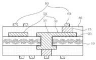
종래에는 빌드업 공정으로 다층 인쇄회로기판을 제조하는 경우, 내부 회로층 위에 절연층을 적층하고 내부 회로층의 비아가 형성될 위치에 레이저 가공을 하여 비아홀을 형성하였다. 그러나, 도 1에 도시된 바와 같이, 레이저 가공법으로 비아홀(3)을 형성하는 경우 레이저의 특성상 비아홀(3)의 형상이 원추형이 되어 비아홀(3)의 지름이 내부 회로층(1) 방향으로 감소하는 형상이 되며, 이러한 형상의 비아홀(3)은 비아홀의 지름이 일정한 경우보다 비아보다 물리적 특성이 저하되는 문제점이 있었다.Conventionally, when a multilayer printed circuit board is manufactured by a build-up process, an insulating layer is stacked on an inner circuit layer, and a via hole is formed by laser processing at a position where a via of the inner circuit layer is to be formed. However, as shown in FIG. 1, when the
또한, 종래에는 상기와 같은 형상의 비아홀에 전해 필(fill) 도금 또는 도전성 페이스트를 충진하는 것으로 비아를 형성하였다. 종래의 전해 필 도금 방식으로 형성된 비아는 비아홀 도금과 패턴의 도금을 동시에 진행하므로 공정오차를 고려하여 회로패턴의 폭보다 큰 랜드부(5)를 구비할 것이 요구되었으며, 이러한 랜드부(5)의 존재로 비아가 형성된 부분의 회로패턴의 고밀도화가 어려운 문제점이 있 었다. 더욱이, 금속분말과 수지재료를 혼합하여 제조하는 도전성 페이스트는 금속에 비해 전기 신호 전달 성능이 저하되는 문제점이 있었다.In addition, in the related art, vias are formed by filling electrolytic fill plating or conductive paste into via holes having the above shapes. Since the via formed by the conventional electrolytic peel plating method simultaneously performs the via hole plating and the plating of the pattern, it is required to have a
본 발명은 상기와 같은 종래기술의 문제점을 해결하고자 창출된 것으로써, 전해 도금층으로 형성된 원기둥 형상의 비아를 구비하여 층간 전기도통이 양호한 인쇄회로기판 및 그 제조방법을 제안한다.The present invention has been made to solve the problems of the prior art as described above, and proposes a printed circuit board having a good electrical conduction between layers and having a cylindrical via formed from an electroplating layer.
또한, 비아 상부에 접속하는 회로패턴의 라인 폭을 비아 직경보다 작게 형성하여 고밀도 회로패턴을 구현할 수 있는 인쇄회로기판 및 그 제조방법을 제안한다.In addition, a printed circuit board and a method of manufacturing the same, which can realize a high density circuit pattern by forming a line width of a circuit pattern connected to an upper portion of a via smaller than a via diameter, are proposed.
본 발명에 따른 인쇄회로기판은, 절연층 하부에 형성된 랜드, 상기 절연층 상부에 형성된 회로패턴 및 상기 랜드와 상기 회로패턴을 전기적으로 접속하는 비아를 포함하고, 상기 랜드는 시드층 및 일면이 상기 시드층과 접속하고 타면이 상기 비아와 연결된 제1 전해 도금층을 포함하고, 상기 비아는 제2 전해 도금층으로 이루어진 것을 그 특징으로 한다.The printed circuit board according to the present invention includes a land formed under the insulating layer, a circuit pattern formed on the insulating layer, and a via electrically connecting the land and the circuit pattern, wherein the land has a seed layer and one surface thereof. And a first electroplating layer connected to the seed layer and connected to the via on the other side thereof, wherein the via is made of a second electroplating layer.
본 발명의 바람직한 한 특징으로서, 상기 비아는 원기둥 형상인 것에 있다.As a preferable feature of the present invention, the via is in a cylindrical shape.
본 발명의 바람직한 또 다른 특징으로서, 상기 회로패턴의 폭은 상기 비아의 직경보다 작은 것에 있다.As another preferable feature of the present invention, the width of the circuit pattern is smaller than the diameter of the via.
본 발명에 따른 인쇄회로기판의 제조방법은, (A) 절연재를 구비하는 코어기판의 전면에 시드층을 형성하는 단계; (B) 상기 시드층 위에 비아의 랜드를 포함하는 제1 회로층 형성용 개구부를 구비하는 제1 레지스트층을 형성하는 단계; (C) 상 기 개구부를 도금하여 제1 회로층을 형성하는 단계; (D) 상기 랜드가 노출되도록 상기 제1 회로층 위에 비아홀을 구비하는 제2 레지스트층을 형성하는 단계; (E) 상기 비아홀을 도금하여 비아를 형성하는 단계; (F) 상기 제1 레지스트층 및 상기 제2 레지스트층을 제거하고, 상기 제1 회로층이 형성되지 않은 부분의 상기 절연재를 노출시키는 단계; (G) 상기 제1 회로층 위에 절연층을 적층하는 단계; 및 (H) 상기 절연층 위에 상기 비아 상면에 접속하는 회로패턴을 포함하는 제2 회로층을 형성하는 단계;를 포함하는 것을 그 특징으로 한다.The method of manufacturing a printed circuit board according to the present invention includes the steps of: (A) forming a seed layer on the front surface of the core substrate having an insulating material; (B) forming a first resist layer having an opening for forming a first circuit layer including lands of vias on the seed layer; (C) plating the opening to form a first circuit layer; (D) forming a second resist layer having via holes on the first circuit layer to expose the lands; (E) plating the via holes to form vias; (F) removing the first resist layer and the second resist layer and exposing the insulating material in a portion where the first circuit layer is not formed; (G) stacking an insulating layer on the first circuit layer; And (H) forming a second circuit layer including a circuit pattern connected to the upper surface of the via on the insulating layer.
본 발명의 바람직한 한 특징으로서, 상기 (H) 단계에서, 상기 비아 상면에 접속하는 상기 회로패턴의 라인 폭은 상기 비아의 직경보다 작은 것에 있다.As a preferable feature of the present invention, in the step (H), the line width of the circuit pattern connected to the upper surface of the via is smaller than the diameter of the via.
본 발명의 바람직한 또 다른 특징으로서, 상기 절연층을 적층하는 단계 이후에, 상기 비아가 상기 절연층 위로 노출되도록 상기 절연층의 일부를 두께방향으로 제거하는 공정을 수행하는 단계를 더 포함하는 것에 있다.In still another aspect of the present invention, after the step of stacking the insulating layer, the method further includes a step of removing a portion of the insulating layer in a thickness direction so that the via is exposed over the insulating layer. .
본 발명의 바람직한 또 다른 특징으로서, 상기 제2 레지스트층의 두께는 30㎛보다 큰 것에 있다.As another preferable feature of the present invention, the thickness of the second resist layer is larger than 30 µm.
본 발명의 바람직한 또 다른 특징으로서, 상기 코어기판은 수지기판, 단면동박적층판 또는 양면동박적층판인 것에 있다.In another preferred aspect of the present invention, the core substrate is a resin substrate, a single-side copper laminated board or a double-sided copper laminated board.
본 발명의 바람직한 또 다른 특징으로서, 상기 (A) 단계 내지 (G) 단계로 제조된 기판을 상기 (A) 단계의 코어기판으로 사용하여 상기 (A) 단계 내지 (H) 단계의 공정을 수행하는 것에 있다.As another preferred feature of the present invention, the step (A) to (G) is used as the core substrate of the step (A) to perform the steps of (A) to (H) Is in.
본 발명의 특징 및 이점들은 첨부도면에 의거한 다음의 상세한 설명으로 더욱 명백해질 것이다.The features and advantages of the present invention will become more apparent from the following detailed description based on the accompanying drawings.
이에 앞서 본 명세서 및 청구범위에 사용된 용어나 단어는 통상적이고 사전적인 의미로 해석되어서는 아니되며, 발명자가 그 자신의 발명을 가장 최선의 방법으로 설명하기 위해 용어의 개념을 적절하게 정의할 수 있다는 원칙에 입각하여 본 발명의 기술적 사상에 부합되는 의미와 개념으로 해석되어야만 한다.Prior to this, the terms or words used in this specification and claims are not to be interpreted in a conventional and dictionary sense, and the inventors may appropriately define the concept of terms in order to best describe their own invention. It should be interpreted as meaning and concept corresponding to the technical idea of the present invention based on the principle that the present invention.
본 발명에 따른 인쇄회로기판은 전해 도금층으로 이루어지는 원기둥 형상의 비아를 포함하기 때문에 층간 전기 도통이 양호하며 단부의 면적이 넓기 때문에 열적변화에 따른 물리적 안정성이 뛰어나다.Since the printed circuit board according to the present invention includes cylindrical vias made of an electrolytic plating layer, electrical conduction between layers is good, and the end area is wide, and thus physical stability due to thermal changes is excellent.
또한, 본 발명에 따른 인쇄회로기판의 비아는 상부랜드가 없어 비아 상부에 형성되는 회로층의 회로패턴을 미세하게 형성할 수 있는 이점이 있다.In addition, the via of the printed circuit board according to the present invention has no advantage of having an upper land so that the circuit pattern of the circuit layer formed on the via is finely formed.
또한, 본 발명에 따른 인쇄회로기판의 제조방법에 따르면, 동일한 시드층을 인입선으로 사용하여 제1 회로층과 비아를 전해 도금하여 형성하기 때문에 제조공정이 간소하다는 이점이 있으며 비아를 형성하기 위한 레이저 가공공정이 제거되므로 제조원가를 절감할 수 있다.In addition, according to the method of manufacturing a printed circuit board according to the present invention, since the first seed layer and the via are formed by electroplating using the same seed layer as a lead line, the manufacturing process is simple and the laser for forming the via is advantageous. Since the machining process is eliminated, manufacturing cost can be reduced.
이하, 본 발명에 따른 인쇄회로기판 및 그 제조방법의 바람직한 실시예를 첨부된 도면을 참조하여 상세히 설명하면 다음과 같다. 첨부된 도면의 전체에 걸쳐, 동일하거나 대응하는 구성요소는 동일한 도면부호로 지칭되며, 중복되는 설명은 생 략한다. 본 명세서에서, 제1, 제2 등의 용어는 하나의 구성요소를 다른 구성요소로부터 구별하기 위한 용도로 사용된 것으로, 구성요소가 상기 용어들에 의해 제한되는 것은 아니다.Hereinafter, a preferred embodiment of a printed circuit board and a method of manufacturing the same according to the present invention will be described in detail with reference to the accompanying drawings. Throughout the accompanying drawings, the same or corresponding components are referred to by the same reference numerals, and overlapping descriptions are omitted. In this specification, the terms first, second, etc. are used to distinguish one component from another component, and the component is not limited by the terms.
도 2는 본 발명의 바람직한 실시예에 따른 인쇄회로기판의 단면도이다. 도 2에 도시된 바와 같이, 본 발명은 절연층(80) 하부에 형성된 랜드(53), 절연층(80) 상부에 형성된 회로패턴(63) 및 랜드(53)와 회로패턴(63)을 전기적으로 접속하는 비아(75)를 포함하는 구성이다.2 is a cross-sectional view of a printed circuit board according to a preferred embodiment of the present invention. As shown in FIG. 2, the present invention electrically connects the
상기 랜드(53)는 시드층(20)과 시드층(20) 위에 형성된 제1 전해 도금층(51)으로 이루어진다.The
상기 비아(75)는 절연층(80)을 사이에 두는 랜드(53)와 회로패턴(63)을 전기적으로 연결하는 구성이다. 비아(75)는 제2 전해 도금층으로 구성되고, 랜드(53)의 제1 전해 도금층(51) 위에, 즉, 시드층(20)과 접하지 않는 랜드(53)의 제1 전해 도금층(51)의 면에 연결된다. 비아(75)는 원기둥 형상으로 직경이 일정하고, 비아(75)의 외주면이 랜드(53)의 접촉면과 수직을 이룬다.The
상기 회로패턴(63)은 비아(75)의 상면에 면접하는 전도성 라인이다. 본 실시예의 회로패턴(63)은 비아(75)의 상면을 가로질러 면접촉하는 구성이며, 회로패턴(63)의 라인 폭은 접속하는 비아(75)의 직경보다 작다. 그러나 본 발명의 회로패턴(63) 형상이 이에 한정되는 것은 아니며, 비아(75)의 직경보다 크거나 동일한 폭을 갖는 회로패턴(63)을 형성할 수 있음을 이해하여야 한다. The
상술한 바와 같이, 본 실시예의 비아(75)는 제2 전해 도금층으로 이루어지고 원기둥 형상이기 때문에 본원의 비아(75)와 동일한 부피를 가지는 다른 형상 및 다른 재료로 이루어지는 비아에 비해 전기적 특성이 뛰어나다.As described above, since the
또한, 실시예의 비아(75)는 상부랜드가 없어 비아(75) 상부 회로패턴(63)을 미세하게 형성할 수 있다. 게다가, 본 실시예의 회로패턴(63)은 비아(75)의 상면을 가로질러 면접촉하기 때문에 비아(75) 내벽 도금층에 접속하는 회로패턴을 가지는 기존의 인쇄회로기판에 비해 전기접속이 양호하다.In addition, since the
이하, 본 발명의 바람직한 실시예에 따른 인쇄회로기판의 제조방법에 대해 서술한다. 도 3은 본 발명의 실시예에 따른 인쇄회로기판의 제조방법을 공정순서대로 도시한 도면이다.Hereinafter, a method of manufacturing a printed circuit board according to a preferred embodiment of the present invention will be described. 3 is a diagram illustrating a method of manufacturing a printed circuit board according to an exemplary embodiment of the present invention in a process sequence.
먼저, 세미어디티브(Semi-additive) 공법 또는 수정된 세미 어디티브 공정(MSAP : Modified semi additive Process)으로 제1 회로층(50)을 형성한다. 여기서는 세미어디티브(Semi-additive) 공법으로 제1 회로층(50)을 형성하는 공정을 간략히 서술한다.First, the
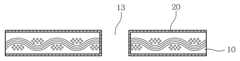
도 3a에 도시된 바와 같이, 코어기판(10)이 제공되고, 코어기판(10)에 관통홀(13)을 형성한다(도 3b). 여기서, 코어기판(10)은 절연재를 구비하는 기판으로, 수지기판, 단면동박적층판 및 양면동박적층판이 될 수 있다. 즉, 본 실시예에서는 수지기판을 코어기판(10)으로 사용하는 것으로 도시 및 서술하지만 이에 제한되는 것은 아니며, 코어기판(10)은 수지기판 이외에 1㎛ 내지 3㎛의 동박이 적층된 동박적층판을 사용하는 것이 가능함을 이해하여야 한다.As shown in FIG. 3A, a
이후, 도 3c에 도시된 바와 같이, 코어기판(10)의 전면에 무전해 동도금을 실시하여 코어기판(10)의 표면 및 관통홀(13)의 내벽에 시드층(20)을 형성한다. 시드층(20) 형성 공정은 예를 들면, 탈지(cleanet) 과정, 소프트 에칭(soft etching) 과정, 예비 촉매처리(pre-catalyst) 과정, 촉매처리 과정, 활성화(accelerator) 과정, 무전해 동도금 과정 및 산화방지 처리 과정을 포함하는 촉매 석출 방식을 이용할 수 있다.Thereafter, as shown in FIG. 3C, the electroless copper plating is performed on the entire surface of the
이후, 도 3d에 도시된 바와 같이, 시드층(20) 위에 감광성 레지스트 필름을 도포하여 제1 레지스트층(30)을 형성하고, 노광 및 현상하여 제1 회로층(50) 형성용 개구부(33)를 형성한다(도 3e). 제1 레지스트층(30) 상에 제1 회로층(50)의 패턴이 인쇄된 포토마스크를 밀착시킨 후, 자외선을 조사한다. 이때, 포토마스크의 인쇄되지 않은 부분은 자외선이 투과하여 포토마스크 아래의 제1 레지스트층(30)에 경화된 부분을 형성하고, 포토마스크의 인쇄된 검은 부분은 자외선이 투과하지 못하여 포토마스크 아래의 제1 레지스트층(30)에 경화되지 않은 부분을 형성한다. 이후, 포토마스크를 제거한 후, 제1 레지스트층(30)의 경화된 부분이 남도록 현상 공정을 수행하여 제1 레지스트층(30)의 경화되지 않은 부분을 제거하여 개구부(33)를 형성한다.Thereafter, as shown in FIG. 3D, a photosensitive resist film is coated on the
그 다음, 도 3f에 도시된 바와 같이, 전해 동도금을 실시하여, 전해 동도금층(51)을 형성한다. 제1 레지스트층(30)의 경화된 부분을 도금 레지스트(plating resist)로 사용하여 전해 동도금을 수행함으로써, 시드층(20) 상에 제1 전해 도금층(51)을 형성한다. 본 실시예에서 제1 전해 도금층(51)을 형성하는 방법은 기판을 동도금 작업통에 침식시킨 후 직류 정류기를 이용하여 전해 동도금을 수행한다. 이러한 전해 동도금은 도금될 면적을 계산하여 직류 정류기에 적당한 전류를 동을 석출하는 방식을 사용하는 것이 바람직하다.Next, as shown in FIG. 3F, electrolytic copper plating is performed to form an electrolytic
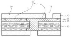
그 다음, 도 3g에 도시된 바와 같이, 전해 동도금층(51) 및 제1 레지스트층(30) 위에 감광성 레지스트를 도포하여 제2 레지스트층(70)을 형성한다. 이때, 기판의 층간 간격 및 기판제조의 공정 신뢰성을 확보를 고려하여 제2 레지스트층(70)은 두께가 30㎛ 이상인 것이 바람직하다.Next, as shown in FIG. 3G, a photosensitive resist is coated on the electrolytic
이후, 도 3h에 도시된 바와 같이, 전해 동도금층(51)의 랜드가 형성될 위치가 노출되도록 제2 레지스트층(70)을 노광 및 현상하여 비아홀(73)을 형성한다. 본 실시예의 제2 레지스트층(70)에 형성되는 비아홀(73)은 감광성 레지스트 필름인 제2 레지스트층의 노광 및 현상에 의해 형성되기 때문에 비아홀(73)의 직경이 랜드(53)부에 근접한 부분에서도 줄어들지 않는 원기둥 형상이 될 수 있다. 즉, 하층패턴 위에 절연층(80)을 적층하고 레이저 가공에 의해 형성된 직경이 줄어드는 형상의 종래의 비아홀과 구별된다.Thereafter, as shown in FIG. 3H, the via
그 다음, 도 3i에 도시된 바와 같이, 전해 동도금을 실시하여 제2 레지스트층(70)의 비아홀(73) 내부에 전해 도금층 만으로 구성되는 비아(75)를 형성한다. 비아(75)를 구성하는 전해 도금층은 제1 회로층(50)을 구성하는 제1 전해 도금층(51)과 구별하기 위한 목적으로 "제2 전해 도금층"이라 명명한다. 동도금 공정은 동도금층의 물리적 특성이 무전해 도금층보다 우수하고, 두꺼운 동도금층을 형성하기에 용이하다. 본 실시예에서, 전해 동도금을 위한 인입선으로 시드층(20)을 사용하므로 별도의 인입선 형성이 필요없다.Next, as shown in FIG. 3I, electrolytic copper plating is performed to form
상기 공정으로 형성된 비아(75)는 원기둥 형상이다. 형성된 비아(75)가 상면 및 하면의 직경이 동일한 원기둥 형상이기 때문에 원추형상의 비아(75)에 비해 전기도통 성능이 향상된다. 또한, 제2 전해 도금층만으로 형성되기 때문에 통상적으로 금속분말에 에폭시수지, 페놀수지, 포화폴리에스테르수지, 불포화폴리에스테르수지, 폴리우레탄수지 등을 바인더로 혼합하여 이루어지는 도전성 페이스트로 형성된 비아에 비해 전기 도통 성능이 향상됨을 본 기술분야의 당업자라면 충분히 이해할 수 있을 것이다.The
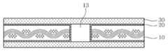
이후, 도 3j에 도시된 바와 같이, 제2 레지스트층(70) 및 제1 레지스트층(30)을 제거하고, 플레쉬 에칭(flash etching)으로 시드층(20)의 노출부를 제거하여 제1 회로층(50)을 완성한다(도 3k). 만약, 코어기판(10)으로 동박적층판을 사용한 경우에는 제1 회로층이 형성되지 않은 부분의 시드층 및 동박을 제거하여 코어기판(10)의 절연재를 노출시킨다.Thereafter, as shown in FIG. 3J, the first circuit layer is removed by removing the second resist
이후, 도 3l에 도시된 바와 같이, 제1 회로층(50) 위에 절연층(80)을 적층한다. 이때 적층되는 절연층(80)이 비아(75)의 상면을 살짝 덮도록 비아(75)의 높이보다 높게 형성한다. 이때, 비아(75) 상부로 절연층(80)의 두께(d1)가 2㎛ 내지 3㎛ 로 유지하는 것이 바람직하다.Thereafter, as illustrated in FIG. 3L, an insulating
이후, 도 3m에 도시된 바와 같이, 화학적 디스미어 공정을 수행하여 비아(75)의 상면이 노출되도록 절연층(80)의 일부를 두께방향으로 제거한다. 예를 들면, KMnO4를 이용하여 절연층(80)의 표면을 깎아내고 화학 동도금시에 절연층(80)과의 접착력을 향상시키기 위한 디스미어(desmear)처리를 수행한다.Thereafter, as illustrated in FIG. 3M, a portion of the insulating
이후, 도 3n에 도시된 바와 같이, 절연층(80) 위에 비아(75)와 접속하는 회로패턴(63)을 구비하는 제2 회로층(60)을 형성하여 인쇄회로기판을 완성한다. 본 실시예에서는 세미어디티브공법(SAP)으로 제2회로층을 형성한다. 이때, 비아(75)가 미리 형성되어 있기 때문에 비아(75)와 접하는 제2 회로층(60)의 회로패턴(63)의 라인 폭을 비아(75)의 직경보다 작게 할 수 있다. 즉, 비아(75) 위에 형성된 회로패턴(63)의 폭을 비아(75) 직경보다 작게 형성하여도 신뢰성 높은 비아(75)의 형성이 가능하다.Thereafter, as shown in FIG. 3N, a
본 실시예에서는 코어기판(10)에 1개의 회로층을 추가 형성하는 것을 도시 및 서술하였으나 이에 제한되는 것은 아니고 본 명세서에 기재된 방식으로 추가의 회로층을 더 형성하는 것도 가능하다. 즉, 상술한 절연층(80)을 적층하고 디스미어 공정을 마친 기판을 본 제조방법 시작부의 코어기판(10)으로 사용함으로써 2층 이상의 회로층을 추가 형성할 수 있다.In the present embodiment, the addition of one circuit layer to the
한편 본 발명은 기재된 실시예에 한정되는 것이 아니고, 본 발명의 사상 및 범위를 벗어나지 않고 다양하게 수정 및 변형을 할 수 있음은 이 기술 분야에서 통상의 지식을 가진 자에게는 자명하다. 따라서, 그러한 변형예 또는 수정예들은 본 발명의 특허청구범위에 속한다 해야 할 것이다.On the other hand, the present invention is not limited to the described embodiments, it is apparent to those skilled in the art that various modifications and variations can be made without departing from the spirit and scope of the present invention. Therefore, such modifications or variations will have to belong to the claims of the present invention.
도 1은 종래의 레이저 가공에 의해 형성된 비아홀을 포함하는 인쇄회뢰기판의 단면도이다.1 is a cross-sectional view of a printed circuit board including via holes formed by conventional laser processing.
도 2는 본 발명의 바람직한 실시예에 따른 인쇄회로기판의 단면도이다.2 is a cross-sectional view of a printed circuit board according to a preferred embodiment of the present invention.
도 3은 본 발명의 바람직한 실시예에 따른 인쇄회로기판의 제조과정을 공정순서대로 도시하는 도면이다.3 is a diagram illustrating a manufacturing process of a printed circuit board according to a preferred embodiment of the present invention in the order of process.
<도면의 주요부호에 대한 설명><Description of Major Symbols in Drawing>
10 코어기판13 관통홀10
20 시드층30 제1 레지스트층20
33 개구부50 제1 회로층33
51 제1 전해 도금층53 랜드51
60 제2 회로층63 회로패턴60
70 제2 레지스트73 비아홀70 Second Resist 73 Via Hole
75 비아75 vias
Claims (9)
Translated fromKoreanPriority Applications (3)
| Application Number | Priority Date | Filing Date | Title |
|---|---|---|---|
| KR1020080036182AKR20090110596A (en) | 2008-04-18 | 2008-04-18 | Printed Circuit Board and Manufacturing Method |
| US12/215,413US20090260868A1 (en) | 2008-04-18 | 2008-06-27 | Printed circuit board and method of manufacturing the same |
| JP2008172357AJP2009260204A (en) | 2008-04-18 | 2008-07-01 | Printed circuit board and method of manufacturing the same |
Applications Claiming Priority (1)
| Application Number | Priority Date | Filing Date | Title |
|---|---|---|---|
| KR1020080036182AKR20090110596A (en) | 2008-04-18 | 2008-04-18 | Printed Circuit Board and Manufacturing Method |
Publications (1)
| Publication Number | Publication Date |
|---|---|
| KR20090110596Atrue KR20090110596A (en) | 2009-10-22 |
Family
ID=41200171
Family Applications (1)
| Application Number | Title | Priority Date | Filing Date |
|---|---|---|---|
| KR1020080036182ACeasedKR20090110596A (en) | 2008-04-18 | 2008-04-18 | Printed Circuit Board and Manufacturing Method |
Country Status (3)
| Country | Link |
|---|---|
| US (1) | US20090260868A1 (en) |
| JP (1) | JP2009260204A (en) |
| KR (1) | KR20090110596A (en) |
Cited By (1)
| Publication number | Priority date | Publication date | Assignee | Title |
|---|---|---|---|---|
| US11439026B2 (en) | 2019-06-24 | 2022-09-06 | Samsung Electro-Mechanics Co., Ltd. | Printed circuit board |
Families Citing this family (13)
| Publication number | Priority date | Publication date | Assignee | Title |
|---|---|---|---|---|
| JP5565950B2 (en)* | 2010-08-23 | 2014-08-06 | 京セラSlcテクノロジー株式会社 | Wiring board manufacturing method |
| KR101085476B1 (en) | 2010-10-25 | 2011-11-21 | 삼성전기주식회사 | Printed Circuit Board Manufacturing Method |
| CN102281724B (en)* | 2011-08-26 | 2013-05-22 | 广州杰赛科技股份有限公司 | Method for machining double-sided windowed plug hole |
| CN104221135B (en)* | 2012-03-29 | 2017-10-24 | 绿点高新科技股份有限公司 | Double-sided circuit board and its preparation method |
| US20140027163A1 (en)* | 2012-07-30 | 2014-01-30 | Samsung Electro-Mechanics Co., Ltd. | Printed circuit board and method for manufacturing the same |
| KR101420520B1 (en)* | 2012-11-07 | 2014-07-17 | 삼성전기주식회사 | A printed circuit board and a method of manufacturing the same |
| KR20150003505A (en)* | 2013-07-01 | 2015-01-09 | 삼성전기주식회사 | Printed circuit board and method of fabricating the same |
| JP2015023251A (en)* | 2013-07-23 | 2015-02-02 | ソニー株式会社 | Multilayer wiring board and manufacturing method therefor, and semiconductor product |
| JP2016100581A (en)* | 2014-11-26 | 2016-05-30 | 京セラサーキットソリューションズ株式会社 | Wiring board manufacturing method |
| JP2017028079A (en)* | 2015-07-22 | 2017-02-02 | イビデン株式会社 | Manufacturing method of printed wiring board and printed wiring board |
| JP6943681B2 (en)* | 2017-08-24 | 2021-10-06 | 住友電気工業株式会社 | Printed wiring board |
| CN114615807A (en)* | 2020-12-09 | 2022-06-10 | 迅达科技公司 | Apparatus and method for forming PCB engineered thermal pathways using auxiliary conductive layers |
| WO2024048713A1 (en)* | 2022-08-31 | 2024-03-07 | 京セラ株式会社 | Printed wiring board and method for manufacturing same |
Family Cites Families (7)
| Publication number | Priority date | Publication date | Assignee | Title |
|---|---|---|---|---|
| US4487654A (en)* | 1983-10-27 | 1984-12-11 | Ael Microtel Limited | Method of manufacturing printed wiring boards |
| JPH06268377A (en)* | 1993-03-17 | 1994-09-22 | Oki Electric Ind Co Ltd | Manufacture of multilayer interconnection board |
| JPH06302965A (en)* | 1993-04-16 | 1994-10-28 | Oki Electric Ind Co Ltd | Formation of via in thin film multilayered substrate |
| KR100687548B1 (en)* | 1999-01-27 | 2007-02-27 | 신꼬오덴기 고교 가부시키가이샤 | Semiconductor wafer manufacturing method, semiconductor device manufacturing method and chip size semiconductor wafer package manufacturing method |
| JP2002043741A (en)* | 2000-07-31 | 2002-02-08 | Toppan Printing Co Ltd | Manufacturing method of printed wiring board |
| JP3807312B2 (en)* | 2002-01-18 | 2006-08-09 | 富士通株式会社 | Printed circuit board and manufacturing method thereof |
| JP2008021784A (en)* | 2006-07-12 | 2008-01-31 | Cmk Corp | Printed wiring board having fine wiring circuit and manufacturing method thereof |
- 2008
- 2008-04-18KRKR1020080036182Apatent/KR20090110596A/ennot_activeCeased
- 2008-06-27USUS12/215,413patent/US20090260868A1/ennot_activeAbandoned
- 2008-07-01JPJP2008172357Apatent/JP2009260204A/enactivePending
Cited By (1)
| Publication number | Priority date | Publication date | Assignee | Title |
|---|---|---|---|---|
| US11439026B2 (en) | 2019-06-24 | 2022-09-06 | Samsung Electro-Mechanics Co., Ltd. | Printed circuit board |
Also Published As
| Publication number | Publication date |
|---|---|
| US20090260868A1 (en) | 2009-10-22 |
| JP2009260204A (en) | 2009-11-05 |
Similar Documents
| Publication | Publication Date | Title |
|---|---|---|
| KR20090110596A (en) | Printed Circuit Board and Manufacturing Method | |
| US8400782B2 (en) | Wiring board and method for manufacturing the same | |
| JP5198105B2 (en) | Manufacturing method of multilayer flexible printed wiring board | |
| KR100728754B1 (en) | Printed Circuit Board Using Bump and Manufacturing Method Thereof | |
| KR100965341B1 (en) | Manufacturing method of printed circuit board | |
| JP2008016482A (en) | Manufacturing method of multilayer printed wiring board | |
| JP5908003B2 (en) | Printed circuit board and printed circuit board manufacturing method | |
| CN1798485B (en) | Multilayer printed circuit board and manufacturing method thereof | |
| CN101959376B (en) | The manufacture method of multilayer flexible printed wiring plate | |
| KR100969439B1 (en) | Method of manufacturing a printed circuit board with landless vias | |
| JP2008311612A (en) | Multilayer printed circuit board, and method of manufacturing the same | |
| CN102308679B (en) | Method of manufacturing multi-layered printed circuit board | |
| KR100744994B1 (en) | Multilayer printed circuit board and its manufacturing method | |
| CN101422091B (en) | Multilayer circuit board having cable section, and manufacturing method thereof | |
| KR100752017B1 (en) | Manufacturing method of printed circuit board | |
| JP3596374B2 (en) | Manufacturing method of multilayer printed wiring board | |
| KR20090078518A (en) | Printed Circuit Board and Manufacturing Method | |
| KR100726238B1 (en) | Multi-layer printed circuit board manufacturing method | |
| JP4813204B2 (en) | Multilayer circuit board manufacturing method | |
| KR100704920B1 (en) | Printed circuit board and manufacturing method using bump board | |
| KR20040061410A (en) | PCB with the plated through holes filled with copper with copper and the fabricating method thereof | |
| JP4319917B2 (en) | Manufacturing method of component built-in wiring board | |
| JP2010016061A (en) | Printed wiring board, and manufacturing method therefor | |
| CN102026489A (en) | Method for manufacturing circuit board | |
| KR100658437B1 (en) | Printed circuit board and manufacturing method using bump board |
Legal Events
| Date | Code | Title | Description |
|---|---|---|---|
| A201 | Request for examination | ||
| PA0109 | Patent application | Patent event code:PA01091R01D Comment text:Patent Application Patent event date:20080418 | |
| PA0201 | Request for examination | ||
| PG1501 | Laying open of application | ||
| E902 | Notification of reason for refusal | ||
| PE0902 | Notice of grounds for rejection | Comment text:Notification of reason for refusal Patent event date:20100203 Patent event code:PE09021S01D | |
| E601 | Decision to refuse application | ||
| PE0601 | Decision on rejection of patent | Patent event date:20100809 Comment text:Decision to Refuse Application Patent event code:PE06012S01D Patent event date:20100203 Comment text:Notification of reason for refusal Patent event code:PE06011S01I |