KR20090097295A - TDD wireless communication system and method using digital predistortion method - Google Patents
TDD wireless communication system and method using digital predistortion methodDownload PDFInfo
- Publication number
- KR20090097295A KR20090097295AKR1020080022348AKR20080022348AKR20090097295AKR 20090097295 AKR20090097295 AKR 20090097295AKR 1020080022348 AKR1020080022348 AKR 1020080022348AKR 20080022348 AKR20080022348 AKR 20080022348AKR 20090097295 AKR20090097295 AKR 20090097295A
- Authority
- KR
- South Korea
- Prior art keywords
- signal
- digital
- tdd
- analog
- distortion
- Prior art date
- Legal status (The legal status is an assumption and is not a legal conclusion. Google has not performed a legal analysis and makes no representation as to the accuracy of the status listed.)
- Ceased
Links
- 238000000034methodMethods0.000titleclaimsabstractdescription91
- 238000004891communicationMethods0.000titleclaimsabstractdescription33
- 230000006854communicationEffects0.000titleclaimsabstractdescription33
- 238000012545processingMethods0.000claimsabstractdescription66
- 230000008030eliminationEffects0.000claimsabstractdescription10
- 238000003379elimination reactionMethods0.000claimsabstractdescription10
- 230000007274generation of a signal involved in cell-cell signalingEffects0.000claimsabstractdescription5
- 230000003044adaptive effectEffects0.000claimsdescription7
- 238000012546transferMethods0.000claimsdescription3
- 230000008901benefitEffects0.000abstractdescription10
- 238000013461designMethods0.000abstractdescription9
- 239000000306componentSubstances0.000description20
- 238000006243chemical reactionMethods0.000description12
- 230000003287optical effectEffects0.000description7
- 230000005540biological transmissionEffects0.000description6
- 238000010586diagramMethods0.000description6
- 238000005516engineering processMethods0.000description5
- 238000010295mobile communicationMethods0.000description5
- 238000010276constructionMethods0.000description3
- 238000009434installationMethods0.000description3
- 230000008054signal transmissionEffects0.000description3
- 230000003321amplificationEffects0.000description2
- 230000002238attenuated effectEffects0.000description2
- 239000000969carrierSubstances0.000description2
- 230000006872improvementEffects0.000description2
- 238000003199nucleic acid amplification methodMethods0.000description2
- 230000008569processEffects0.000description2
- 230000009467reductionEffects0.000description2
- 230000003595spectral effectEffects0.000description2
- 238000013459approachMethods0.000description1
- 230000007175bidirectional communicationEffects0.000description1
- 230000008859changeEffects0.000description1
- 239000008358core componentSubstances0.000description1
- 238000012937correctionMethods0.000description1
- 230000008878couplingEffects0.000description1
- 238000010168coupling processMethods0.000description1
- 238000005859coupling reactionMethods0.000description1
- 230000000694effectsEffects0.000description1
- 238000001914filtrationMethods0.000description1
- 238000003780insertionMethods0.000description1
- 230000037431insertionEffects0.000description1
- 230000007774longtermEffects0.000description1
- 238000012423maintenanceMethods0.000description1
- 238000004519manufacturing processMethods0.000description1
- 238000012986modificationMethods0.000description1
- 230000004048modificationEffects0.000description1
- 238000005457optimizationMethods0.000description1
- 230000035755proliferationEffects0.000description1
- 238000006467substitution reactionMethods0.000description1
Images


Classifications
- H—ELECTRICITY
- H04—ELECTRIC COMMUNICATION TECHNIQUE
- H04B—TRANSMISSION
- H04B1/00—Details of transmission systems, not covered by a single one of groups H04B3/00 - H04B13/00; Details of transmission systems not characterised by the medium used for transmission
- H04B1/38—Transceivers, i.e. devices in which transmitter and receiver form a structural unit and in which at least one part is used for functions of transmitting and receiving
- H04B1/40—Circuits
- H04B1/44—Transmit/receive switching
- H—ELECTRICITY
- H04—ELECTRIC COMMUNICATION TECHNIQUE
- H04B—TRANSMISSION
- H04B1/00—Details of transmission systems, not covered by a single one of groups H04B3/00 - H04B13/00; Details of transmission systems not characterised by the medium used for transmission
- H04B1/62—Details of transmission systems, not covered by a single one of groups H04B3/00 - H04B13/00; Details of transmission systems not characterised by the medium used for transmission for providing a predistortion of the signal in the transmitter and corresponding correction in the receiver, e.g. for improving the signal/noise ratio
Landscapes
- Engineering & Computer Science (AREA)
- Computer Networks & Wireless Communication (AREA)
- Signal Processing (AREA)
- Amplifiers (AREA)
Abstract
Translated fromKoreanDescription
Translated fromKorean본 발명은 TDD(Time Division Duplex) 방식의 무선통신 시스템 및 그 방법에 관한 것으로, 더욱 상세하게는 전력 증폭기의 선형성을 높이기 위해 디지털 전치왜곡(Digital Pre-Distortion) 방식을 적용하여 구현한 TDD 무선통신 시스템 및 그 방법에 관한 것이다.The present invention relates to a wireless communication system and a method of the TDD (Time Division Duplex) method, and more particularly to the TDD wireless communication implemented by applying a digital pre-distortion method to increase the linearity of the power amplifier. A system and method thereof are provided.
이하의 본 발명의 일실시예에서는 TDD 무선통신 시스템의 일예로, PAPR(Peak to Average Power Ratio) 특성이 높은 OFDM(Orthogonal Frequency Division Multiplexing) 방식의 휴대 인터넷 시스템(일명 모바일 와이맥스 또는 와이브로라고도 함)을 포함한 TDD 방식의 RRF(Remote Radio Frequency) 시스템을 예로 들어 설명하기로 하나, 본 발명이 이에 한정되는 것이 아님을 미리 밝혀둔다.In the following embodiment of the present invention, as an example of a TDD wireless communication system, an Orthogonal Frequency Division Multiplexing (OFDM) portable Internet system (also referred to as mobile WiMAX or WiBro) having a high PAPR (Peak to Average Power Ratio) characteristic is used. Although a description will be given taking an example of a TDD type RRF system, the present invention is not limited thereto.
여기서, RRF 시스템은 기존의 기지국 내에서 처리하는 베이스밴드와 RF(Radio Frequency) 신호처리 기능을 디지털부와 RF부로 구분하여, 디지털부 기능만을 기지국에 남겨두고 RF부 기능을 원거리에서 구현하는 방식으로, 기지국에서 광으로 송신한 디지털 기저대역 신호를 RF 신호로 변환하여 무선으로 송신 또는 그 역기능을 수행한다.Here, the RRF system divides the baseband and RF (Radio Frequency) signal processing functions that are processed in the existing base station into a digital unit and an RF unit, leaving only the digital unit functions in the base station and implementing the RF unit functions at a long distance. In addition, the base station converts the digital baseband signal transmitted by the optical into an RF signal and wirelessly transmits or performs the reverse function.
또한, 본 발명에서는, 기지국에서 단말기로의 신호 전달 방향을 순방향이라 하고, 단말기에서 기지국으로의 신호 전달 방향을 역방향이라고 하기로 한다.In the present invention, the signal transmission direction from the base station to the terminal is referred to as a forward direction, and the signal transmission direction from the terminal to the base station is referred to as a reverse direction.
이동전화 서비스를 베어러 서비스로 제공하는 기존 이동통신망은 음성통화로의 항시 연결을 제공하기 위해 기지국과 사용자 단말기 간의 양방향 통신 신호 전달 경로를 상향과 하향 주파수 대역으로 분리하여 사용하는 FDD(Frequency Division Duplex) 방식으로 무선망을 구축하였다. 그러나 1990년대 말 xDSL을 시작으로 초고속 인터넷의 보급이 확산됨에 따라 이동 무선환경에서도 고속의 데이터 통신에 대한 필요성이 증가하면서 2005년 초 2.3GHz 주파수를 사용하여 xDSL 수준의 통신품질과 비용으로 정지 및 이동 중에도 고속의 통신 서비스가 가능한 휴대 인터넷 서비스 제공 사업자를 발표하였다.Existing mobile communication networks that provide mobile phone services as bearer services use FDD (Frequency Division Duplex), which uses two-way communication paths between base stations and user terminals in uplink and downlink frequency bands to provide a continuous connection to voice calls. The wireless network was established in the method. However, with the proliferation of high-speed internet, starting with xDSL in the late 1990s, the need for high-speed data communication in mobile wireless environment has increased.In early 2005, the 2.3GHz frequency was used to stop and move at xDSL-level communication quality and cost. The company announced a mobile Internet service provider that enables high-speed communication services.
휴대 인터넷은 이동 무선환경에서의 고속 데이터 통신을 제공하기 위하여 기존의 이동통신망 기술과 달리 주파수자원의 효율적인 사용을 위해 기지국과 사용자 단말기 간의 양방향 통신신호 전달경로를 주파수 대역이 아닌 상향과 하향 전송 시간으로 분리하여 사용하는 TDD 방식과 고속 데이터 전송에 적합한 것으로 알려진 OFDM/OFDMA(Orthogonal Frequency Division Multiple Access) 방식을 시스템 기술로 채택하였다.The portable Internet, unlike the existing mobile communication network technology, provides high-speed data communication in a mobile wireless environment, and the bidirectional communication signal transmission path between a base station and a user terminal does not correspond to a frequency band in uplink and downlink transmission time for efficient use of frequency resources. The TDD scheme and the Orthogonal Frequency Division Multiple Access (OFDM) scheme, which are known to be suitable for high-speed data transmission, are adopted as system technologies.
이동 무선환경에서 원활한 통신을 제공하기 위해서는, 제공하고자 하는 서비 스에 채택된 기술 방식과 대상 서비스에 대한 사용자의 통신 수요를 예측하여 무선망을 구축하게 된다. 무선망을 구축하는 방식은 기지국을 실내 또는 실외에 설치하여 사용자 단말기에 직접 전달하는 방식이 있으며, 대상 서비스의 제공 영역인 커버지리를 확장하고 통신신호가 전달되지 않는 음영지역을 해결하기 위해 기지국과 사용자 단말기 중간에 통신신호를 중계하는 RF 유니트인 중계기를 설치하는 방식이 있다.In order to provide smooth communication in a mobile wireless environment, a wireless network is constructed by predicting a communication scheme of a user for a target service and a technology scheme adopted for a service to be provided. The wireless network can be constructed by installing a base station indoors or outdoors and delivering it directly to a user terminal.The base station is provided with a base station to expand the coverage geography, which is a service providing area, and to solve a shadow area where communication signals are not transmitted. There is a method of installing a repeater which is an RF unit for relaying a communication signal in the middle of the user terminal.
중계기는 기지국 신호를 중계하기 위해 사용되는 매체에 따라 광 중계기, RF(Radio Frequency) 중계기, IF(Intermediate Frequency) 중계기, 마이크로웨이브 중계기 등이 있으며, 기지국과 중계기 간에 전송되는 전송신호에 따라 아날로그 중계기와 디지털 중계기가 있으며, 설치되는 장소에 따라 인빌딩 중계기, 지하철 중계기, 터널 중계기 등이 있다. 이동 무선환경에서의 무선망 구축에는 광 중계기, RF 중계기, 인빌딩 중계기가 많이 사용되는데, 광 중계기는 가격이 비싸다는 단점이 있으며, RF 중계기는 설치 장소 및 효율에 제약이 있으며, 인빌딩 중계기는 설치 비용이 높다. 이와 같은 단점을 어느 정도 보완하려는 목적에서 나온 솔루션이 RRF(Remote Radio Frequency) 시스템이다.Repeaters include optical repeaters, RF (Radio Frequency) repeaters, IF (Intermediate Frequency) repeaters, and microwave repeaters, depending on the medium used to relay the base station signals. There are digital repeaters and there are in-building repeaters, subway repeaters and tunnel repeaters depending on where they are installed. Optical repeaters, RF repeaters, and in-building repeaters are frequently used to construct a wireless network in a mobile wireless environment. Optical repeaters have a disadvantage in that they are expensive. RF repeaters have limitations on installation location and efficiency. Installation cost is high. A solution that aims to compensate for this drawback to some extent is the RRF (Remote Radio Frequency) system.
상기 RRF(Remote RF) 시스템은 전술한 바와 같이 기존의 기지국 내에서 처리하는 베이스밴드와 RF 신호처리 기능을 디지털부와 RF(Radio Frequency)부로 구분하여, 디지털부 기능만을 기지국에 남겨두고 RF부 기능을 원거리에서 구현하는 방식으로, 기존의 무선망 구축 방식에 비해 기능이 축소된 기지국은 집중화하여 설치하고, 서비스를 제공하고자 하는 복수 개의 RRF 시스템을 광케이블을 통해 상기 기 지국에 연결하게 된다.The RRF (Remote RF) system divides the baseband and RF signal processing functions processed in the existing base station into a digital unit and an RF (Radio Frequency) unit as described above, leaving only the digital unit function in the base station and the RF unit function. In a long-range implementation, the base station having reduced functionality compared to the conventional wireless network construction method is installed centrally and connects a plurality of RRF systems to provide a service to the base station through an optical cable.
따라서 RRF 방식을 적용한 무선망 구조는 기지국의 기능 축소 및 기지국 설치/유지 보수의 편이성으로 인한 가격 하락과 더불어 광케이블을 통해 복수 개의 RRF 시스템을 캐스케이드(Cascade) 또는 링(Ring) 형태로 구성함으로써, 이론적으로 한 개의 기지국에 수 개 내지 수십 개의 RRF 시스템의 연결을 가능하게 함으로써 망 최적화에 유연성을 부여할 수 있다. 이와 같은 기지국과 RRF 시스템 간의 인터페이스에 대해서는 CPRI(Common Public Radio Interface) 또는 OBSAI(Open Base Station Standard Initiative) 단체 등에서 기존 FDD 방식의 3GPP(3rd Generation Partnership Project), 3GPP2와 TDD 방식의 "802.16e/WiMAX", LTE(Long-Term Evolution)에서 채택한 기술 방식을 지원하도록 표준화 작업을 진행하고 있다.Therefore, the wireless network structure using the RRF method is theoretically formed by cascading or ringing a plurality of RRF systems through an optical cable together with a price drop due to the reduction of function of the base station and the ease of base station installation / maintenance. As a result, several to dozens of RRF systems can be connected to one base station, thereby providing flexibility in network optimization. As for the interface between the base station and the RRF system, the 3rd Generation Partnership Project (3GPP), 3GPP2 and TDD type "802.16e / WiMAX of the existing FDD method, such as the Common Public Radio Interface (CPRI) or Open Base Station Standard Initiative (OBSAI) group, etc. "We are working on standardization to support the technology approach adopted by Long-Term Evolution (LTE).
다음으로, 도 1을 참조하여 기존의 TDD 방식의 RRF 시스템에 대하여 살펴보면 다음과 같다.Next, referring to FIG. 1, an RRF system of a conventional TDD scheme is as follows.
도 1은 기존의 TDD 방식의 RRF 시스템의 일실시예 구성도이다.1 is a diagram illustrating an embodiment of a conventional RDD system using a TDD scheme.
도 1에 도시된 바와 같이, RRF 시스템(20)은 기지국(디지털 베이스밴드부)(10)과 디지털 I/Q 신호를 주고받게 되므로, 기지국(10)은 기저대역 신호처리만을 수행하는 디지털 베이스밴드부 기능을 중심으로 설계되고, RRF 시스템(20)은 아날로그-디지털 변환을 처리하기 위한 아날로그-디지털 변환기(ADC)/디지털-아날로그 변환기(DAC)와 RF-IF 변환 기능을 수행하기 위한 주파수 상향/하향 변환기(LO, VCO/PLL, 주파수 믹서로 이루어짐), 증폭 기능을 수행하기 위한 증폭기(고전력 증 폭기(HPA), 저잡음 증폭기(LNA)), 기지국 내의 제어부(또는 외부의 제어부)로부터의 TDD 타이밍 신호(제어 신호)에 따라 스위칭되어 순방향 링크 또는 역방향 링크를 설정하기 위한 두 개의 스위치(TDD SPST switch), 서큘레이터(Circulator), 및 대역통과필터(BPF) 등으로 이루어진 아날로그 유니트로 설계된다.As shown in FIG. 1, since the
상기와 같은 RRF 시스템(20)에서는 안테나를 통해 RF 신호가 송출되었을 때 공간에서 급격히 감쇄되는 RF 신호의 크기를 증폭하기 위해 RF 송신단에 고전력 증폭기(HPA : High Power Amplifier)(30)를 사용한다. 도 1에 도시된 바와 같이, 고전력 증폭기(HPA, 30)는 RF 송신단의 최종단에 위치하여 수 GHz 대의 신호를 증폭하여 안테나로 전달하는 역할을 수행하기 때문에 RF부의 구성요소 중에서 전력소모가 가장 많이 소모되는 핵심부품이며, 타 통신부품에 비해 고가이다.In the
이때, 상기 고전력 증폭기(HPA, 30)는 신호 증폭을 위해 능동소자를 이용하기 때문에 선형성, 이득, 최대출력전력, 및 전력효율 등으로 특성화되고, 상기 각 특성 상호 간에 밀접한 연관 관계를 맺으며, 송신 신호의 RF 성능 규격 중 RCE(Relative Constellation Error), 스펙트럴 마스크(Spectral Mask), 스퓨리어스 발사(Spurious Emission) 등에 결정적인 영향을 미치게 된다. 즉, 고전력 증폭기(HPA, 30)는 선형성 지표 중 하나인 P1 dB에서 증폭기의 동작점을 백-오프(Back-off)시킬수록 출력신호의 선형성은 좋아지나, 최대 출력전력 및 전력효율은 감소하게 된다. 반면에, 상기 고전력 증폭기(HPA, 30)는 증폭기로의 입력신호를 증가시키면 최대 출력전력 및 전력효율은 향상되지만, 선형성이 열화되어 송신 신호의 RCE(Relative Constellation Error), 스펙트럴 마스크(Spectral Mask), 스퓨리어스 발사(Spurious Emission) 등이 나빠지는 트레이드-오프 관계를 갖는다.In this case, the high power amplifier (HPA) 30 is characterized by linearity, gain, maximum output power, power efficiency, etc., since it uses active elements for signal amplification, and has a close relationship with each other and transmits. The RF performance specifications of the signal have a decisive influence on RCE (Relative Constellation Error), Spectral Mask, and Spurious Emission. That is, the high power amplifier (HPA) 30 improves the linearity of the output signal as the back-off of the operating point of the amplifier at P1 dB, which is one of the linearity indicators, but reduces the maximum output power and power efficiency. do. On the other hand, the high power amplifier (HPA) 30 improves the maximum output power and power efficiency by increasing the input signal to the amplifier, but linearity deteriorates, so that RCE (Relative Constellation Error) and spectral mask of the transmission signal are deteriorated. ), Spurious emission (Spurious Emission) and the like has a bad trade-off relationship.
한편, 이동통신 시스템에서 수 개의 RF 캐리어를 전달하는 기지국은, 넓은 대역폭과 낮은 인접 채널 누설비(ACLR : Adjacent Channel Leakage Ratio)를 가지면서 고출력을 제공하는 선형 전력 증폭기(LPA : Linear Power Amplifier)의 확보가 필수적이다. 이때, 전력 증폭기(고전력 증폭기)의 선형성을 향상시키는 위해서는 전력 증폭기 제작에 사용되는 능동소자에서 발생되는 비선형 요소들을 적절한 회로를 구성하여 제거하는 방법이 있으며, 이를 위한 회로 구조로서 피드백(feedback) 방식, 피드포워드(feed-forward) 방식, 전치왜곡(pre-distortion) 방식 등이 있다. 상기 여러 방식 중에서 전치왜곡 방식은 전력 증폭기의 비선형 특성과 반대가 되도록 입력신호를 사전에 왜곡하여 전력 증폭기에 입력함으로써, 전력 증폭기의 출력신호에서 왜곡성분이 상쇄되어 출력신호가 선형성을 갖도록 하는 방법이다.Meanwhile, a base station delivering several RF carriers in a mobile communication system has a large bandwidth and a low Adjacent Channel Leakage Ratio (ACLR) while providing a high power linear power amplifier (LPA) of a linear power amplifier (LPA). Securing is essential. In this case, in order to improve the linearity of the power amplifier (high power amplifier), there is a method of removing a non-linear element generated from the active element used in manufacturing the power amplifier by configuring an appropriate circuit, a feedback structure (feedback) method, There is a feed-forward method, a pre-distortion method, and the like. The predistortion method is a method in which the input signal is distorted in advance so as to be opposite to the nonlinear characteristics of the power amplifier and inputted to the power amplifier so that the distortion component is canceled from the output signal of the power amplifier so that the output signal has linearity. .
이러한 전치왜곡 방식의 장점은 피드포워드 방식에 비해 왜곡 제거 루프에 사용되는 보조 증폭기가 없기 때문에 구조가 간단하므로 소형으로 제작할 수 있고, 부가적인 디씨(DC) 전력소모가 없어 효율이 좋다는 점이다. 또한, 전치왜곡 방식은 비용 면에서도 피드포워드 방식보다 저렴하다. 또한, 전치왜곡 방식은 왜곡 보정이 전력 증폭기의 입력 전단에서 이루어지므로 삽입 손실을 쉽게 보상할 수 있는 장점이 있다. 또한, 전치왜곡 방식은 피드포워드 방식과 마찬가지로 개방형-루프(open loop) 구조이므로 안정화되어 있어, 피드백 방식에 비해 대역폭의 제한을 덜 받는 다.The advantage of this predistortion method is that since there is no auxiliary amplifier used in the distortion canceling loop compared to the feed forward method, the structure is simple, so it can be manufactured compactly, and there is no additional DC power consumption, so it is efficient. Also, the predistortion method is cheaper than the feedforward method in terms of cost. In addition, the predistortion method has an advantage of easily compensating insertion loss since the distortion correction is performed at the front end of the power amplifier. In addition, the predistortion method is stabilized since it is an open-loop structure like the feedforward method, and thus is less limited in bandwidth than the feedback method.
상기 전치왜곡 방식은 왜곡 제거 루프를 통해 생성되는 신호의 특성에 따라 아날로그 전치왜곡 방식과 디지털 전치왜곡 방식으로 구분되는데, 디지털 전치왜곡 방식은 기존의 아날로그 전치왜곡 방식에 비해 선형성 개선 성능이 더 우수하며, 피드포워드 방식에 비해 경량화 및 소형화를 이룰 수 있는 장점이 있다. 또한, 디지털 전치왜곡 방식은, 방식 자체가 오차의 피드백을 통한 적응 제어(adaptive control) 방식으로 이루어지므로, 오차 허용 한계 측면에서 피드포워드 방식보다 장점을 가지고 있다.The predistortion method is classified into an analog predistortion method and a digital predistortion method according to the characteristics of the signal generated through the distortion elimination loop. The digital predistortion method has better linearity improvement performance than the conventional analog predistortion method. In comparison with the feedforward method, there is an advantage that weight and size can be achieved. In addition, the digital predistortion method has an advantage over the feedforward method in terms of error tolerance, since the method itself is made of an adaptive control method through error feedback.
다음으로, 도 2를 참조하여 기존의 디지털 전치왜곡 방식을 적용한 TDD 방식의 RRF 시스템에 대하여 살펴보면 다음과 같다.Next, referring to FIG. 2, the TRF RRF system to which the conventional digital predistortion method is applied is as follows.
도 2는 기존의 디지털 전치왜곡 방식을 적용한 TDD 방식의 RRF 시스템의 일실시예 구성도이다.2 is a diagram illustrating an embodiment of a TRF RRF system using a conventional digital predistortion method.
도 2의 설명에 있어서, 상기 도 1에서 전술한 구성요소 및 그 동작에 대해서는 설명을 생략하기로 한다.In the description of FIG. 2, the description of the components described above and the operation thereof in FIG. 1 will be omitted.
도 2에 도시된 바와 같이, 디지털 전치왜곡 방식은 고전력 증폭기(HPA, 30)의 비선형 특성을 보정하기 위해, 고전력 증폭기(HPA, 30)의 비선형 특성의 역함수에 해당하는 기능을 모델링하여 전치왜곡기를 통해 출력되는 디지털 신호의 크기와 위상을 변경하여 고전력 증폭기(HPA, 30)의 비선형성 왜곡성분을 보상해준다. 이를 위해 디지털 전치왜곡 방식은 기저대역의 디지털 왜곡신호를 생성하기 위한 왜곡 제거 루프 회로와 오차 신호의 적응 제어를 위한 부가 회로를 구성해야 한다.As shown in FIG. 2, the digital predistortion method uses a predistorter by modeling a function corresponding to an inverse function of the nonlinear characteristics of the high power amplifier (HPA) 30 to correct the nonlinear characteristics of the high power amplifier (HPA) 30. It compensates for the nonlinear distortion component of the high power amplifier (HPA) by changing the magnitude and phase of the digital signal. To this end, the digital predistortion method must configure a distortion cancellation loop circuit for generating a baseband digital distortion signal and an additional circuit for adaptive control of an error signal.
도 2에서는 왜곡 제거 루프 회로와 부가 회로를 위한 구성요소(DPD 블록, 40)로서 감쇄기, 주파수 하향 변환기(41), 아날로그-디지털 변환기(42), 디지털 전치왜곡 신호를 적응 제어하기 위한 디지털 신호처리 프로세서(DSP : Digital Signal Processor), 고전력 증폭기(HPA, 30)의 비선형 특성의 역함수에 해당하는 디지털 전치왜곡 신호 값을 미리 계산하여 저장하고 있다가 로딩하여 주는 룩업테이블(LUT), 및 상기 룩업테이블(LUT)로부터의 디지털 전치왜곡 신호 값에 따라 디지털 기저대역 신호의 크기와 위상을 변경하여 고전력 증폭기(HPA, 30)의 비선형성 왜곡성분을 보상하기 위한 전치왜곡기(Pre-D)를 포함한다.In FIG. 2, digital signal processing for adaptive control of an attenuator, a
한편, 이동통신 시스템의 RF부에서 디지털 기저대역 신호와 아날로그 RF 신호의 상호 변환을 위해 RF 신호를 기저대역 신호로 직접 변환하는 Zero-IF(즉, Direct Conversion) 또는 중간 주파수를 사용하는 IF(즉, 수퍼헤테로다인) 방식이 사용될 수 있다. 이를 위해 아날로그 RF 프론트엔드 구현에 있어서는 주파수 변환을 위해 IF 또는 RF 캐리어로의 신호 변환을 위한 발진기(LO, VCO/PLL), 주파수 믹서 및 대역통과필터 등을 필요로 한다.In the meantime, the RF part of the mobile communication system uses zero-IF (i.e., direct conversion) or intermediate frequency (i.e., direct conversion) that directly converts an RF signal to a baseband signal for mutual conversion between a digital baseband signal and an analog RF signal. , Superheterodyne) may be used. To achieve this, analog RF front-end implementations require oscillators (LO, VCO / PLL), frequency mixers, and bandpass filters for signal conversion to IF or RF carriers for frequency conversion.
상기 도 2에 도시된 바와 같이, TDD 방식의 이동통신망 구축에 있어 디지털 전치왜곡 방식을 이용한 RRF 시스템을 이용하는 경우, 전력 증폭기(고전력 증폭기)의 선형성은 개선할 수 있으나, 디지털 전치왜곡 신호를 생성하기 위하여 수 개의 RF 캐리어 신호를 기저대역 신호로 변환하기 위해서는 사용자 신호의 처리와 별도로 디지털 전치왜곡 신호를 생성하기 위한 별도의 주파수 하향 변환기(41)와 아날로그-디지털 변환기(42)를 필요로 하게 되는 단점이 있다.As shown in FIG. 2, in the case of using the RRF system using the digital predistortion method in the construction of the TDD mobile communication network, the linearity of the power amplifier (high power amplifier) can be improved, but the digital predistortion signal is generated. In order to convert several RF carrier signals into baseband signals, a separate frequency down
즉, 상기와 같은 종래 기술은, 전력 증폭기의 선형성을 개선하기 위해 RF부에 디지털 전치왜곡 방식을 적용하기 위해서, 전용의 RF 부품을 필요로 하게 됨에 따라 별도의 배선 설계와 소자를 탑재할 공간을 사용하게 되므로 비용 측면에서 최적화된 방법이라고 할 수 없는 문제점이 있으며, 이러한 문제점을 해결하고자 하는 것이 본 발명의 과제이다.In other words, the prior art as described above requires a dedicated RF component in order to apply the digital predistortion method to the RF unit in order to improve linearity of the power amplifier. Since there is a problem that can not be called an optimized method in terms of cost, it is an object of the present invention to solve this problem.
따라서 본 발명은 디지털 전치왜곡 방식을 이용하여 전력 증폭기의 선형성을 개선하면서 RF 단의 부품소자의 공용화를 통해 설계 및 배선의 용이함과 더불어 부품소자의 수를 줄여 경제적으로 무선망을 구축할 수 있도록 하기 위한, TDD 무선통신 시스템 및 그 방법을 제공하는데 그 목적이 있다.Therefore, the present invention improves the linearity of the power amplifier by using the digital predistortion method, so that it is possible to construct a wireless network economically by reducing the number of components and the ease of design and wiring through the common use of the components of the RF stage. An object of the present invention is to provide a TDD wireless communication system and a method thereof.
즉, 본 발명은 디지털 전치왜곡 방식을 이용하여 전력 증폭기의 선형성을 개선하기 위해, 디지털 전치왜곡 신호를 생성하기 위한 왜곡 제거 루프(DPD Feedback loop)를 구성할 때, RF 파트에서 역방향 신호처리 기능을 담당하는 부품을 공용으 로 사용함으로써 디지털 전치왜곡 방식에 따른 성능 향상, RF 파트의 부품 공용화, 및 무선망 설계에 있어 유연성있는 시스템 도입에 따른 경제적인 이득을 획득할 수 있는, TDD 무선통신 시스템 및 그 방법을 제공하는데 그 목적이 있다.That is, the present invention provides a reverse signal processing function in an RF part when constructing a DPD feedback loop for generating a digital predistortion signal in order to improve the linearity of the power amplifier using the digital predistortion method. TDD wireless communication system that can obtain the economic benefits of improving performance according to digital predistortion method, sharing parts of RF parts, and adopting flexible system in wireless network design by using shared parts in common. The purpose is to provide a method.
본 발명의 목적들은 이상에서 언급한 목적으로 제한되지 않으며, 언급되지 않은 본 발명의 다른 목적 및 장점들은 하기의 설명에 의해서 이해될 수 있으며, 본 발명의 실시예에 의해 보다 분명하게 알게 될 것이다. 또한, 본 발명의 목적 및 장점들은 특허 청구 범위에 나타낸 수단 및 그 조합에 의해 실현될 수 있음을 쉽게 알 수 있을 것이다.The objects of the present invention are not limited to the above-mentioned objects, and other objects and advantages of the present invention which are not mentioned above can be understood by the following description, and will be more clearly understood by the embodiments of the present invention. Also, it will be readily appreciated that the objects and advantages of the present invention may be realized by the means and combinations thereof indicated in the claims.
상기 목적을 달성하기 위한 본 발명의 장치는, TDD(Time Division Duplex) 무선통신 시스템에 있어서, 고전력 증폭기의 비선형 특성의 역함수에 해당하는 디지털 전치왜곡 신호 값을 이용하여 디지털 기저대역 신호를 전치왜곡시키기 위한 디지털 전치왜곡 수단; TDD 타이밍 신호에 따라 스위칭되어 왜곡 제거 루프와 순방향 링크를 형성하거나 역방향 링크를 형성하기 위한 TDD 스위칭 수단; 및 상기 TDD 스위칭 수단의 스위칭에 따라 역방향 링크의 RF(Radio Frequency) 소자를 공용하여 왜곡 제거 루프를 형성하여 기저대역의 디지털 왜곡신호를 생성하여 상기 디지털 전치왜곡 수단으로 피드백시키기 위한 디지털 왜곡신호 생성 수단을 포함한다.An apparatus of the present invention for achieving the above object, in a time division duplex (TDD) wireless communication system, predistorting a digital baseband signal using a digital predistortion signal value corresponding to the inverse of the nonlinear characteristic of the high power amplifier Digital predistortion means for; TDD switching means for switching in accordance with the TDD timing signal to form a forward link with the distortion cancellation loop or a reverse link; And digital distortion signal generation means for sharing a reverse frequency RF (Radio Frequency) element in accordance with the switching of the TDD switching means to form a distortion elimination loop to generate a baseband digital distortion signal and to feed it back to the digital predistortion means. It includes.
한편, 상기 목적을 달성하기 위한 본 발명의 방법은, TDD(Time Division Duplex) 무선통신 시스템에서의 디지털 전치왜곡 방법에 있어서, 고전력 증폭기의 비선형 특성의 역함수에 해당하는 디지털 전치왜곡 신호 값을 이용하여 디지털 기저대역 신호를 전치왜곡시키는 디지털 전치왜곡 단계; TDD 타이밍 신호에 따라 스위칭되어 왜곡 제거 루프와 순방향 링크를 형성하거나 역방향 링크를 형성하는 TDD 스위칭 단계; 및 상기 TDD 스위칭 단계에서의 스위칭에 따라 역방향 링크의 RF(Radio Frequency) 소자를 공용하여 왜곡 제거 루프를 형성하여 기저대역의 디지털 왜곡신호를 생성하여 상기 디지털 전치왜곡 단계로 피드백시키는 디지털 왜곡신호 생성 단계를 포함한다.On the other hand, the method of the present invention for achieving the above object, in the digital predistortion method in a time division duplex (TDD) wireless communication system, by using a digital predistortion signal value corresponding to the inverse function of the nonlinear characteristic of the high power amplifier A digital predistortion step of predistorting the digital baseband signal; A TDD switching step of switching according to the TDD timing signal to form a forward link with the distortion canceling loop or a reverse link; And a digital distortion signal generation step of sharing a reverse frequency RF (Radio Frequency) element in accordance with the switching in the TDD switching step to form a distortion elimination loop to generate a baseband digital distortion signal and to feed it back to the digital predistortion step. It includes.
이처럼, 본 발명은 기지국에서 광으로 송신한 디지털 기저대역 신호를 RF 신호로 변환하여 무선으로 송신 또는 그 역기능을 수행하는 RRF 시스템의 구조 설계에 있어, 가격 및 시스템의 면적에 주요 영향을 미치는 전력 증폭기의 선형성 개선을 위해 디지털 전치왜곡(DPD : Digital Pre-Distortion) 방식을 적용한 TDD 방식의 RRF 시스템 구조에서, 역방향 링크의 주파수 하향 변환기와 아날로그-디지털 변환기의 전단에 RF 스위치를 추가하여 순방향 신호처리시간 동안 유휴상태인 고가의 RF 부품소자인 역방향 링크의 주파수 하향 변환기와 아날로그-디지털 변환기를 순방향 링크의 디지털 전치왜곡을 위한 왜곡 제거 루프에 이용할 수 있도록 구현하였다.As described above, the present invention is a power amplifier that has a major influence on the cost and area of the system in the design of the structure of the RRF system that converts the digital baseband signal transmitted from the base station into optical signals to the RF signal and transmits the radio or the reverse function thereof. In the TDD RRF system structure using Digital Pre-Distortion (DPD) method to improve linearity, forward signal processing time is added by adding RF switch in front of reverse frequency converter and analog-to-digital converter in reverse link. The frequency downconverter and analog-to-digital converter of the reverse link, which are expensive RF components, which are idle, can be used for the distortion-reduction loop for digital predistortion of the forward link.
상기와 같은 본 발명은, 휴대 인터넷 시스템을 포함한 TDD 방식의 RRF 시스템 구축에 있어, 성능에 큰 영향을 미치는 전력 증폭기의 선형성을 디지털 전치왜 곡 방식을 이용하여 개선하면서 RF 단의 부품소자의 공용화를 통해 설계 및 배선의 용이함과 더불어 부품소자의 수를 줄임으로써, 경제적으로 무선망을 구축할 수 있도록 하는 효과가 있다.The present invention as described above, in the construction of a TDD RRF system including a portable Internet system, by using a digital predistortion method to improve the linearity of the power amplifier that has a significant impact on the performance of the RF stage components common use By reducing the number of components and components as well as the ease of design and wiring, there is an effect that it is possible to economically build a wireless network.
즉, 본 발명은 디지털 전치왜곡 방식을 이용하여 전력 증폭기의 선형성을 개선하기 위해, 디지털 전치왜곡 신호를 생성하기 위한 왜곡 제거 루프(DPD Feedback loop)를 구성할 때, RF 파트에서 역방향 신호처리 기능을 담당하는 부품(주파수 하향 변환기와 아날로그-디지털 변환기)을 공용으로 사용함으로써 디지털 전치왜곡 방식에 따른 성능 향상, RF 파트의 부품 공용화, 및 무선망 설계에 있어 유연성있는 시스템 도입에 따른 경제적인 이득을 획득할 수 있는 효과가 있다.That is, the present invention provides a reverse signal processing function in an RF part when constructing a DPD feedback loop for generating a digital predistortion signal in order to improve the linearity of the power amplifier using the digital predistortion method. By using the components in common (frequency down converter and analog-to-digital converter) in common, it is possible to improve the performance by digital predistortion method, share parts of the RF part, and gain the economical benefit from the introduction of flexible system in wireless network design. It can work.
즉, 본 발명은 RF부의 성능 및 가격에 있어 중요 부품인 전력 증폭기의 선형성 개선 및 효율을 높이기 위해 디지털 전치왜곡 방식을 도입한 TDD 방식의 RRF 시스템 설계에 있어, 디지털 전치왜곡 신호의 생성을 위한 전력 증폭기 출력신호의 디지털 기저대역 신호로의 변환을 위해, 전용의 주파수 하향 변환기와 아날로그-디지털 변환기를 별도로 구현하지 않고, TDD 방식에 의해 순방향 신호처리시간 동안에는 유휴상태인 역방향 링크의 주파수 하향 변환기와 아날로그-디지털 변환기를 사용함으로써, RF 파트의 시스템 설계 및 배선을 용이하게 하는 한편, 사용되는 부품의 숫자를 줄임으로써 RRF 시스템 도입에 따른 가격 절감과 더불어 추가적인 가격 절감의 효과를 기대할 수 있다.That is, the present invention provides a power for generating a digital predistortion signal in a TDD RRF system design in which a digital predistortion method is introduced to improve the linearity and efficiency of a power amplifier which is an important component in the performance and price of the RF unit. To convert the amplifier output signal into a digital baseband signal, a dedicated frequency downconverter and analog-to-digital converter are not implemented separately, but the reverse link frequency downconverter and analog are idle during the forward signal processing time by the TDD method. By using a digital converter, the system design and wiring of the RF part can be facilitated, while the number of parts used can be reduced, and further cost reduction can be expected with the introduction of the RRF system.
상술한 목적, 특징 및 장점은 첨부된 도면을 참조하여 상세하게 후술되어 있는 상세한 설명을 통하여 보다 명확해 질 것이며, 그에 따라 본 발명이 속하는 기술분야에서 통상의 지식을 가진 자가 본 발명의 기술적 사상을 용이하게 실시할 수 있을 것이다. 또한, 본 발명을 설명함에 있어서 본 발명과 관련된 공지 기술에 대한 구체적인 설명이 본 발명의 요지를 불필요하게 흐릴 수 있다고 판단되는 경우에 그 상세한 설명을 생략하기로 한다. 이하, 첨부된 도면을 참조하여 본 발명에 따른 바람직한 실시예를 상세히 설명하기로 한다.The above objects, features, and advantages will become more apparent from the detailed description given hereinafter with reference to the accompanying drawings, and accordingly, those skilled in the art to which the present invention pertains may share the technical idea of the present invention. It will be easy to implement. In addition, in describing the present invention, when it is determined that the detailed description of the known technology related to the present invention may unnecessarily obscure the gist of the present invention, the detailed description thereof will be omitted. Hereinafter, exemplary embodiments of the present invention will be described in detail with reference to the accompanying drawings.
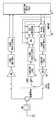
도 3은 본 발명에 따른 디지털 전치왜곡 방식을 이용한 TDD 방식의 RRF 시스템의 일실시예 구성도이다.3 is a configuration diagram of an RRF system of a TDD method using a digital predistortion method according to the present invention.
도 3에 도시된 바와 같이, 본 발명에 따른 디지털 전치왜곡 방식을 이용한 TDD 방식의 RRF 시스템은, 고전력 증폭기(HPA, 30)의 비선형 특성의 역함수에 해당하는 디지털 전치왜곡 신호 값을 이용하여 기지국(10)으로부터의 디지털 기저대역 신호를 전치왜곡시켜 상기 고전력 증폭기(HPA, 30)의 비선형 왜곡성분을 보상하도록 하기 위한 디지털 전치왜곡부(310), 기지국(10) 내의 제어부(또는 외부의 제어부)로부터의 TDD 타이밍 신호(제어 신호)에 따라 스위칭되어 왜곡 제거 루프와 순방향 링크를 형성하거나 역방향 링크를 형성하기 위한 TDD 스위칭부(330), 및 상기 TDD 스위칭부(330)의 스위칭에 따라 역방향 링크의 RF 소자를 공용하여 왜곡 제거 루프를 형성하여 기저대역의 디지털 왜곡신호를 생성하여 상기 디지털 전치왜곡부(310)로 피드백시키기 위한 디지털 왜곡신호 생성부(320)를 포함한다.As shown in FIG. 3, the RRF system of the TDD method using the digital predistortion method according to the present invention uses a base station using a digital predistortion signal value corresponding to an inverse function of the nonlinear characteristic of the high power amplifier (HPA) 30. From the
여기서, 상기 디지털 왜곡신호 생성부(320)는, 상기 TDD 스위칭부(330)의 순향방 링크로의 스위칭에 따라 순방향 송신시간(신호처리시간) 동안 역방향 링크의 주파수 하향 변환기(325)와 역방향 링크의 아날로그-디지털 변환기(326)를 공용하여 왜곡 제거 루프를 형성하여 기저대역의 디지털 왜곡신호를 생성하는 것을 특징으로 한다.Here, the digital distortion
이때, 상기 디지털 왜곡신호 생성부(320)는, 상기 디지털 전치왜곡부(310)에서 전치왜곡된 디지털 기저대역 신호를 아날로그 기저대역 신호로 변환하기 위한 디지털-아날로그 변환기(DAC, 321), 상기 디지털-아날로그 변환기(DAC, 321)에서 변환된 아날로그 기저대역 신호를 아날로그 RF 신호로 주파수 상향 변환하기 위한 주파수 상향 변환기(322), 상기 주파수 상향 변환기(322)에서 변환된 아날로그 RF 신호를 출력전력으로 증폭하면서 증폭단의 비선형 왜곡특성을 상쇄하기 위한 상기 고전력 증폭기(HPA, 30), 상기 고전력 증폭기(HPA, 30)로부터의 출력신호(아날로그 RF 신호) 중 일부 출력신호를 커플링하여 분기(분배)시키기 위한 커플러(323), 상기 커플러(323)를 통하여 분기된 아날로그 RF 신호를 감쇄시키기 위한 감쇄기(324), 상기 감쇄기(324)로부터의 아날로그 RF 신호를 아날로그 기저대역 신호로 주파수 하향 변환하기 위한 역방향 링크의 주파수 하향 변환기(325), 및 상기 역방향 링크의 주파수 하향 변환기(325)로부터의 아날로그 기저대역 신호를 디지털 기저대역 신호로 변환하기 위한 역방향 링크의 아날로그-디지털 변환기(326)를 포함한다.In this case, the digital
여기서, 상기 감쇄기(324)는 본 발명에서 부가 구성요소로서, 상기 감쇄 기(324)를 포함하지 않는 경우에는 상기 커플러(323)를 통하여 분기된 아날로그 RF 신호가 바로 역방향 링크의 주파수 하향 변환기(325)로 전달되어 아날로그 기저대역 신호로 주파수 하향 변환된다.Here, the
그리고 상기 역방향 링크의 주파수 하향 변환기(325)는, TDD 역방향 신호처리시간 동안에는 저잡음 증폭기(344)로부터의 역방향 아날로그 RF 신호를 역방향 아날로그 기저대역 신호로 주파수 하향 변환을 수행하고, TDD 순방향 신호처리시간 동안에는 왜곡 제거 루프를 형성하여 기저대역의 디지털 왜곡신호 생성에 사용된다.The frequency down
즉, 상기 역방향 링크의 주파수 하향 변환기(325)는, TDD 역방향 신호처리시간 동안에는 사용자 단말기 측으로부터 대역통과필터(342)와 저잡음 증폭기(344)를 통해 수신된 역방향 링크의 아날로그 RF 신호를 아날로그 기저대역 신호로 주파수 하향 변환을 수행하고, TDD 순방향 신호처리시간 동안에는 상기 고전력 증폭기(HPA, 30)에서 비선형 왜곡이 상쇄되어 출력된 고출력의 아날로그 RF 신호의 일부가 커플링되고 감쇄되어 피드백되면 해당 아날로그 RF 신호를 아날로그 기저대역 신호로 주파수 하향 변환을 수행한다.That is, the frequency down
이때, 상기 역방향 링크의 주파수 하향 변환기(325)는, 아날로그 RF 신호의 아날로그 기저대역 신호로의 직접 변환을 위해 발진기, 필터, 및 주파수 믹서 등을 포함하여 구성되거나, 중간주파수를 이용한 IF 변환을 위한 RF-IF 변환과 IF-기저대역 변환을 위한 발진기, 필터, 및 주파수 믹서 등을 포함하여 구성된다.In this case, the frequency down
그리고 상기 역방향 링크의 아날로그-디지털 변환기(326)는, TDD 역방향 신 호처리시간 동안에는 상기 역방향 링크의 주파수 하향 변환기(325)로부터의 역방향 아날로그 기저대역 신호를 역방향 디지털 기저대역 신호로 변환하고, TDD 순방향 신호처리시간 동안에는 왜곡 제거 루프를 형성하여 기저대역의 디지털 왜곡신호 생성에 사용된다.The analog-to-
즉, 상기 역방향 링크의 아날로그-디지털 변환기(326)는, TDD 역방향 신호처리시간 동안에는 상기 역방향 링크의 주파수 하향 변환기(325)를 통해 사용자 단말기 측으로부터 수신된 역방향 링크의 아날로그 기저대역 신호를 디지털 기저대역 신호로 변환하고, TDD 순방향 신호처리시간 동안에는 상기 역방향 링크의 주파수 하향 변환기(325)를 통해 상기 고전력 증폭기(HPA, 30) 측으로부터 피드백된 아날로그 기저대역 신호를 디지털 기저대역 신호로 변환한다.That is, the analog-to-
한편, 상기 TDD 스위칭부(330)는, 기지국(10) 내의 제어부(또는 외부의 제어부)로부터의 TDD 타이밍 신호(제어 신호)에 따라, TDD 순방향 신호처리시간 동안에는 상기 역방향 링크의 주파수 하향 변환기(325)와 상기 역방향 링크의 아날로그-디지털 변환기(326)가 기저대역의 디지털 왜곡신호 생성에 사용되고, TDD 역방향 신호처리시간 동안에는 상기 역방향 링크의 주파수 하향 변환기(325)와 상기 역방향 링크의 아날로그-디지털 변환기(326)가 사용자 단말기 측으로부터 수신된 역방향 신호 처리를 수행하도록 스위칭된다.On the other hand, the
즉, 상기 TDD 스위칭부(330)는, TDD 순방향 신호처리시간 동안에는 상기 역방향 링크의 주파수 하향 변환기(325)와 상기 역방향 링크의 아날로그-디지털 변환기(326)가 상기 고전력 증폭기(HPA, 30)의 비선형 왜곡을 상쇄하기 위한 기저대역 의 디지털 왜곡신호 생성에 사용되도록 하고, TDD 역방향 신호처리시간 동안에는 상기 역방향 링크의 주파수 하향 변환기(325)와 상기 역방향 링크의 아날로그-디지털 변환기(326)가 사용자 단말기 측으로부터 대역통과필터(342)와 저잡음 증폭기(344)를 통해 수신된 역방향 링크의 신호 처리를 수행하도록, 기지국(10) 내의 제어부(또는 외부의 제어부)로부터의 TDD 타이밍 신호(제어 신호)에 따라 상기 역방향 링크의 주파수 하향 변환기(325)와 상기 역방향 링크의 아날로그-디지털 변환기(326)의 동작을 순방향 링크와 역방향 링크로 각각 절체하는 기능을 수행한다.That is, the
이때, 상기 TDD 스위칭부(330)는, 기지국(10) 내의 제어부(또는 외부의 제어부)로부터의 TDD 타이밍 신호(제어 신호)에 따라 스위칭되어 TDD 순방향 신호처리시간 동안에는 상기 고전력 증폭기(HPA, 30)로부터의 순방향 신호를 송신단으로 전달하고, TDD 역방향 신호처리시간 동안에는 상기 고전력 증폭기(HPA, 30)로부터의 순방향 신호가 송신단으로 전달되지 않도록 차단하기 위한 제 1 스위치(331), 기지국(10) 내의 제어부(또는 외부의 제어부)로부터의 TDD 타이밍 신호(제어 신호)에 따라 스위칭되어 TDD 순방향 신호처리시간 동안에는 저잡음 증폭기(344)로부터의 역방향 신호가 상기 역방향 링크의 주파수 하향 변환기(325)로 전달되지 않도록 차단하고, TDD 역방향 신호처리시간 동안에는 저잡음 증폭기(344)로부터의 역방향 신호를 상기 역방향 링크의 주파수 하향 변환기(325)로 전달하기 위한 제 2 스위치(332), 및 기지국(10) 내의 제어부(또는 외부의 제어부)로부터의 TDD 타이밍 신호(제어 신호)에 따라 스위칭되어 TDD 순방향 신호처리시간 동안에는 상기 역방향 링크의 아날로그-디지털 변환기(326)로부터의 디지털 기저대역 신호(기저대역의 디 지털 왜곡신호)를 상기 디지털 전치왜곡부(310)로 전달하고, TDD 역방향 신호처리시간 동안에는 상기 역방향 링크의 아날로그-디지털 변환기(326)로부터의 디지털 기저대역 신호를 기지국(10) 측으로 전달하기 위한 제 3 스위치(333)를 포함한다.In this case, the
한편, 상기 디지털 전치왜곡부(310)는, 고전력 증폭기(HPA, 30)의 비선형 특성의 역함수에 해당하는 디지털 전치왜곡(사전왜곡) 신호 값을 미리 계산하여 저장하고 있다가 로딩하여 주는 룩업테이블(LUT, 313), 상기 디지털 왜곡신호 생성부(320)로부터의 기저대역의 디지털 왜곡신호를 이용하여 상기 룩업테이블(LUT, 313)의 디지털 전치왜곡 신호를 적응 제어하기 위한 디지털 신호처리 프로세서(DSP, 312), 및 상기 룩업테이블(LUT, 313)로부터의 디지털 전치왜곡 신호 값에 따라 기지국(10)으로부터의 디지털 기저대역 신호를 전치왜곡시켜(즉, 디지털 기저대역 신호의 크기와 위상을 변경하여) 고전력 증폭기(HPA, 30)의 비선형성 왜곡성분을 보상하도록 하기 위한 전치왜곡기(Pre-D, 311)를 포함한다.Meanwhile, the
여기서, 상기 디지털 전치왜곡부(310)는 도 3의 실시예와 같이 RRF 시스템 내에 구현되거나, 상기 기지국(10) 내에 구현될 수도 있다.Here, the
한편, 기지국(디지털 베이스밴드부, 10)은 TDD 방식의 디지털 기저대역 신호를 처리하여 RRF 시스템의 디지털 전치왜곡부(310)로 전달하는 기능을 담당한다.On the other hand, the base station (digital baseband unit 10) is responsible for processing the digital baseband signal of the TDD system and delivers it to the
다음으로, 본 발명에 따른 디지털 전치왜곡 방식을 이용한 TDD 방식의 RRF 시스템의 동작을 살펴보면 다음과 같다. 이때, 그 구체적인 실시예는 전술한 바와 같으므로, 여기서는 전체적인 동작 흐름을 간략하게 설명하기로 한다.Next, the operation of the TDD RRF system using the digital predistortion method according to the present invention will be described. At this time, since the specific embodiment is as described above, the overall operation flow will be briefly described.
먼저, 기지국(10)으로부터의 디지털 기저대역 신호는 전치왜곡기(311)에서 전치왜곡(사전왜곡)되어 디지털-아날로그 변환기(321)와 주파수 상향 변환기(322)를 통해 아날로그 RF 신호로 변환되어 고전력 증폭기(HPA, 30)로 입력된다. 사전왜곡된 아날로그 RF 신호는 고전력 증폭기(HPA, 30)의 비선형 특성과 반대의 특성을 가지므로 고전력 증폭기(HPA, 30)의 출력신호는 선형 이득을 가진 신호로서, 순방향 송신시간 동안에 TDD 방식에 따라 순방향 링크로 스위칭되는 제 1 스위치(331)를 통과한 후에, 순방향 신호의 역방향 유입을 방지하기 위한 아이솔레이터(341)를 거친 다음에, 대역통과필터(BPF, 342)를 통과하여 안테나를 통해 송출된다.First, the digital baseband signal from the
반대로, 안테나로부터 수신된 아날로그 RF 신호는 주어진 RF 대역 내 신호만을 필터링하기 위한 대역통과필터(BPF, 342)를 거친 후에, 역방향 신호의 순방향 유입을 방지하기 위한 아이솔레이터(341)를 거친 다음에, 역방향 잡음지수를 낮추도록 임피던스 매칭되어 아날로그 RF 신호를 저잡음 증폭을 수행하는 저잡음 증폭기(LNA, 344)를 통과한다. 상기 저잡음 증폭기(344)로부터 출력된 아날로그 RF 신호는 제 2 스위치(332)를 통과하여 주파수 하향 변환기(325)와 아날로그-디지털 변환기(326)에서 디지털 기저대역 신호(디지털 기저대역 I/Q 신호)로 변환된 후, 제 3 스위치(333)를 통해 디지털 기저대역 신호처리를 수행하는 기지국(10)으로 전달된다.Conversely, the analog RF signal received from the antenna passes through a bandpass filter (BPF) 342 for filtering only signals in a given RF band, followed by an
한편, 도 3에서 상기 디지털 전치왜곡부(310)로는 상기 고전력 증폭기(HPA, 30)의 입력신호의 크기와 주파수 대역에 따른 특성 변화를 보상하기 위해 적응 제 어를 담당하는 디지털 신호처리 프로세서(DSP, 312)와 상기 고전력 증폭기(HPA, 30)의 비선형 특성을 보상하기 위해 디지털 전치왜곡 신호 값을 저장하고 있는 룩업테이블(LUT, 313)이 사용되었다. 전력 증폭기의 비선형 특성을 표현하는 방법에는 전력 증폭기의 입력신호의 지연신호까지 포함하여 주파수에 따른 비선형 전달특성까지 표현하는 볼테라 시리즈(Volterra series)로 대표되는 다항식 전치왜곡 방식과, 입력 신호의 크기에 따라 순람표의 색인을 만들고 이 색인을 참조하여 입력신호의 크기와 위상을 변경하여 전치왜곡 신호를 생성하는 룩업테이블(LUT : Lookup Table) 전치왜곡 방식이 있다. 도 3에서는 본 발명의 일실시예를 설명하기 위해 룩업테이블(LUT, 313) 전치왜곡 방식을 사용하였다.Meanwhile, in FIG. 3, the
또한, 도 3에서는 순방향 신호처리시간 동안 송신되는 고전력 증폭기(HPA, 30)의 출력신호를 커플링하여 역방향 신호처리시간 동안 유휴상태(idle time)인 역방향 링크의 주파수 하향 변환기(325)와 아날로그-디지털 변환기(326)를 통해 고전력 증폭기(HPA, 30)의 출력신호를 디지털 왜곡신호(디지털 기저대역 신호)로 변환한 후에 디지털 신호처리 프로세서(DSP, 312)로 입력한다. 그러면, 디지털 신호처리 프로세서(DSP, 312)는 주기적 또는 상기 고전력 증폭기(HPA, 30)의 특성이 변경될 때마다, 상기 고전력 증폭기(HPA, 30)의 역 전달특성을 얻기 위해, 고전력 증폭기(HPA, 30)의 입력신호가 고전력 증폭기(HPA, 30)와 디지털 신호처리 프로세서(DSP, 312)로 이루어진 적응 필터(adaptive filter)를 통해 선형증폭된 신호로 출력될 수 있도록, 적응적으로 디지털 왜곡신호의 크기와 위상을 조절하여 룩업테이블(LUT, 313)의 해당 입력신호의 순람표의 색인을 찾아 갱신하게 된다.In addition, in FIG. 3, the output signal of the high power amplifier (HPA) 30 transmitted during the forward signal processing time is coupled to the frequency down
또한, 상기 전치왜곡기(311)를 통하여 전치왜곡된 신호를 생성하기 위해, 본 발명에서는 도 3에 도시된 바와 같이 TDD 역방향 링크의 주파수 하향 변환기(325)와 아날로그-디지털 변환기(326)를 사용한다. 도 2에서 전술한 바와 같이, RF부 가격의 상당 부분을 차지하는 고전력 증폭기(HPA, 30)의 선형성과 효율을 개선하기 위해 디지털 전치왜곡 방식을 적용하는 데 있어, 디지털 전치왜곡 신호를 생성하기 위해 전용의 주파수 하향 변환기와 아날로그-디지털 변환기를 사용하는 것은 성능대비 경제성 측면에서 그 개선 효과를 반감시킬 수 있다. 그러므로 도 3에 도시된 바와 같이, 휴대 인터넷 시스템을 포함한 TDD 방식 RRF 시스템의 RF부에서 역방향 링크의 주파수 하향 변환기(325)와 아날로그-디지털 변환기(326)가 순방향 신호처리시간 동안에는 유휴상태이므로, 상기 역방향 링크의 주파수 하향 변환기(325)와 아날로그-디지털 변환기(326)를 순방향 신호처리시간 동안 디지털 왜곡신호의 생성에 사용함으로써 RF부의 설계 및 배선을 간단하게 하는 한편, 사용되는 부품 소자의 수를 줄임으로써 제품 가격을 낮출 수가 있다.In addition, in order to generate a predistorted signal through the
한편, 본 발명에 따른 RRF 시스템의 구현에 있어, 도 3에 도시된 바와 같이 전치왜곡기(311)의 적응 제어를 담당하는 디지털 신호처리 프로세서(DSP, 312)와 룩업테이블(LUT, 313)로 이루어진 디지털 전치왜곡부(310)는 왜곡 제거 루프로부터 생성된 기저대역의 디지털 왜곡신호를 입력받아 처리하게 되므로, 시스템으로 구현하는 측면에서 종래의 디지털 기저대역 신호만을 처리하는 기지국(10)에 포함하여 구현할 수도 있고, RRF 시스템 내에 구현할 수도 있다.Meanwhile, in the implementation of the RRF system according to the present invention, as shown in FIG. 3, the digital signal processing processor (DSP) 312 and the lookup table (LUT) 313 in charge of the adaptive control of the
이상에서 설명한 본 발명은, 본 발명이 속하는 기술 분야에서 통상의 지식을 가진 자에게 있어 본 발명의 기술적 사상을 벗어나지 않는 범위 내에서 여러 가지 치환, 변형 및 변경이 가능하므로 전술한 실시예 및 첨부된 도면에 의해 한정되는 것이 아니다.The present invention described above is capable of various substitutions, modifications, and changes without departing from the technical spirit of the present invention for those skilled in the art to which the present invention pertains. It is not limited by the drawings.
본 발명은 TDD 무선통신 시스템 등에 이용될 수 있다.The present invention can be used in a TDD wireless communication system.
도 1은 기존의 TDD 방식의 RRF 시스템의 일실시예 구성도,1 is a configuration diagram of an embodiment of a conventional TRF type RRF system;
도 2는 기존의 디지털 전치왜곡 방식을 적용한 TDD 방식의 RRF 시스템의 일실시예 구성도,2 is a diagram illustrating an embodiment of a TRF RRF system using a conventional digital predistortion method;
도 3은 본 발명에 따른 디지털 전치왜곡 방식을 이용한 TDD 방식의 RRF 시스템의 일실시예 구성도이다.3 is a configuration diagram of an RRF system of a TDD method using a digital predistortion method according to the present invention.
* 도면의 주요 부분에 대한 부호의 설명* Explanation of symbols for the main parts of the drawings
10 : 기지국30 : 고전력 증폭기(HPA)10: base station 30: high power amplifier (HPA)
310 : 디지털 전치왜곡부311 : 전치왜곡기(Pre-D)310: digital predistorter 311: predistorter (Pre-D)
312 : 디지털 신호처리 프로세서313 : 룩업테이블(LUT)312 digital
320 : 디지털 왜곡신호 생성부321 : 디지털-아날로그 변환기(DAC)320: digital distortion signal generator 321: digital-to-analog converter (DAC)
322 : 주파수 상향 변환기323 : 커플러322
324 : 감쇄기325 : 주파수 하향 변환기324
326 : 아날로그-디지털 변환기330 : TDD 스위칭부326: analog-to-digital converter 330: TDD switching unit
331 : 제 1 스위치332 : 제 2 스위치331: first switch 332: second switch
333 : 제 3 스위치333: third switch
Claims (15)
Translated fromKoreanPriority Applications (1)
| Application Number | Priority Date | Filing Date | Title |
|---|---|---|---|
| KR1020080022348AKR20090097295A (en) | 2008-03-11 | 2008-03-11 | TDD wireless communication system and method using digital predistortion method |
Applications Claiming Priority (1)
| Application Number | Priority Date | Filing Date | Title |
|---|---|---|---|
| KR1020080022348AKR20090097295A (en) | 2008-03-11 | 2008-03-11 | TDD wireless communication system and method using digital predistortion method |
Publications (1)
| Publication Number | Publication Date |
|---|---|
| KR20090097295Atrue KR20090097295A (en) | 2009-09-16 |
Family
ID=41356672
Family Applications (1)
| Application Number | Title | Priority Date | Filing Date |
|---|---|---|---|
| KR1020080022348ACeasedKR20090097295A (en) | 2008-03-11 | 2008-03-11 | TDD wireless communication system and method using digital predistortion method |
Country Status (1)
| Country | Link |
|---|---|
| KR (1) | KR20090097295A (en) |
Cited By (6)
| Publication number | Priority date | Publication date | Assignee | Title |
|---|---|---|---|---|
| KR101182146B1 (en)* | 2011-10-31 | 2012-09-12 | 주식회사 쏠리드 | Communication system having non-linear power amplifier and method of controlling the same |
| CN105429916A (en)* | 2015-06-28 | 2016-03-23 | 知鑫知识产权服务(上海)有限公司 | Adaptive digital predistortion method of multiplex receiving link |
| CN109004908A (en)* | 2018-09-11 | 2018-12-14 | 京信通信系统(中国)有限公司 | The power amplifying system of adaptive linear |
| KR20200054845A (en)* | 2018-11-12 | 2020-05-20 | (주) 에이앤티에스 | Mobile communication repeater |
| WO2023121138A1 (en)* | 2021-12-24 | 2023-06-29 | 삼성전자 주식회사 | Apparatus and method for signal compensation in wireless communication system |
| CN119788100A (en)* | 2024-06-25 | 2025-04-08 | 杭州得翼通信技术有限公司 | Communication system |
- 2008
- 2008-03-11KRKR1020080022348Apatent/KR20090097295A/ennot_activeCeased
Cited By (6)
| Publication number | Priority date | Publication date | Assignee | Title |
|---|---|---|---|---|
| KR101182146B1 (en)* | 2011-10-31 | 2012-09-12 | 주식회사 쏠리드 | Communication system having non-linear power amplifier and method of controlling the same |
| CN105429916A (en)* | 2015-06-28 | 2016-03-23 | 知鑫知识产权服务(上海)有限公司 | Adaptive digital predistortion method of multiplex receiving link |
| CN109004908A (en)* | 2018-09-11 | 2018-12-14 | 京信通信系统(中国)有限公司 | The power amplifying system of adaptive linear |
| KR20200054845A (en)* | 2018-11-12 | 2020-05-20 | (주) 에이앤티에스 | Mobile communication repeater |
| WO2023121138A1 (en)* | 2021-12-24 | 2023-06-29 | 삼성전자 주식회사 | Apparatus and method for signal compensation in wireless communication system |
| CN119788100A (en)* | 2024-06-25 | 2025-04-08 | 杭州得翼通信技术有限公司 | Communication system |
Similar Documents
| Publication | Publication Date | Title |
|---|---|---|
| US20190372530A1 (en) | Distributed antenna system architectures | |
| USRE50175E1 (en) | Methods and apparatuses for digital pre-distortion | |
| US20180323813A1 (en) | High efficiency, remotely reconfigurable remote radio head unit system and method for wireless communications | |
| JP5698419B2 (en) | Linearization for a single power amplifier in a multiband transmitter | |
| US7962174B2 (en) | Transceiver architecture and method for wireless base-stations | |
| KR101584372B1 (en) | Multi-dimensional Volterra series transmitter linearization | |
| KR101581470B1 (en) | Minimum Feedback Radio Architecture with Digitally Configurable Adaptive Linearization | |
| US8750410B2 (en) | Multi-band power amplifier digital predistortion system and method | |
| EP3018874B1 (en) | Wireless transceiver | |
| EP1816752B1 (en) | Multi-band multi-standard modular transceiver circuit for wireless communication mobile and base stations | |
| EP2664060B1 (en) | Systems and methods for a radio frequency transmitter with improved linearity and power out utilizing pre-distortion and a gan (gallium nitride) power amplifier device | |
| US10763795B2 (en) | Multi-path communication device for sharing feedback path for digital pre-distortion | |
| CN101534133A (en) | Wireless transceiver | |
| CN101621304A (en) | Transceiver | |
| JP6705918B2 (en) | Wireless device and wireless communication method | |
| KR20090097295A (en) | TDD wireless communication system and method using digital predistortion method | |
| CN101272155B (en) | TDD mode digital predistortion power amplifier | |
| Kardaras et al. | Advanced multimode radio for wireless & mobile broadband communication | |
| US7439895B1 (en) | Linear amplifier using digital feedforward | |
| CN115104261A (en) | Multiband Transmitter | |
| JP6326964B2 (en) | Radio apparatus and distortion compensation control method | |
| KR100781049B1 (en) | Predistortion linearization transceiver of microwave band | |
| Xu et al. | A Partial Band Self-interference Cancellation Scheme for Sub-band Full Duplex | |
| Suzuki et al. | 1.7 GHz/2.1 GHz dual-band feed-forward amplifier |
Legal Events
| Date | Code | Title | Description |
|---|---|---|---|
| PA0109 | Patent application | Patent event code:PA01091R01D Comment text:Patent Application Patent event date:20080311 | |
| A201 | Request for examination | ||
| PA0201 | Request for examination | Patent event code:PA02012R01D Patent event date:20090309 Comment text:Request for Examination of Application Patent event code:PA02011R01I Patent event date:20080311 Comment text:Patent Application | |
| PG1501 | Laying open of application | ||
| E902 | Notification of reason for refusal | ||
| PE0902 | Notice of grounds for rejection | Comment text:Notification of reason for refusal Patent event date:20101030 Patent event code:PE09021S01D | |
| E601 | Decision to refuse application | ||
| PE0601 | Decision on rejection of patent | Patent event date:20110330 Comment text:Decision to Refuse Application Patent event code:PE06012S01D Patent event date:20101030 Comment text:Notification of reason for refusal Patent event code:PE06011S01I |