KR20090087457A - Hybrid Layers for Use on Coatings on Electronic Devices or Other Articles - Google Patents
Hybrid Layers for Use on Coatings on Electronic Devices or Other ArticlesDownload PDFInfo
- Publication number
- KR20090087457A KR20090087457AKR1020097011196AKR20097011196AKR20090087457AKR 20090087457 AKR20090087457 AKR 20090087457AKR 1020097011196 AKR1020097011196 AKR 1020097011196AKR 20097011196 AKR20097011196 AKR 20097011196AKR 20090087457 AKR20090087457 AKR 20090087457A
- Authority
- KR
- South Korea
- Prior art keywords
- hybrid layer
- layer
- hybrid
- polymeric
- precursor material
- Prior art date
- Legal status (The legal status is an assumption and is not a legal conclusion. Google has not performed a legal analysis and makes no representation as to the accuracy of the status listed.)
- Ceased
Links
- 238000000576coating methodMethods0.000titleclaimsabstractdescription40
- 239000000463materialSubstances0.000claimsabstractdescription214
- 238000000034methodMethods0.000claimsabstractdescription126
- 239000002243precursorSubstances0.000claimsabstractdescription93
- 238000000151depositionMethods0.000claimsabstractdescription81
- 239000007789gasSubstances0.000claimsabstractdescription67
- 239000000203mixtureSubstances0.000claimsabstractdescription39
- 238000006243chemical reactionMethods0.000claimsabstractdescription37
- 239000000376reactantSubstances0.000claimsabstractdescription33
- 239000011248coating agentSubstances0.000claimsabstractdescription32
- 238000005229chemical vapour depositionMethods0.000claimsabstractdescription27
- 230000008569processEffects0.000claimsabstractdescription16
- 150000003961organosilicon compoundsChemical class0.000claimsabstractdescription11
- 229920005573silicon-containing polymerPolymers0.000claimsabstractdescription4
- 230000008021depositionEffects0.000claimsdescription58
- QVGXLLKOCUKJST-UHFFFAOYSA-Natomic oxygenChemical compound[O]QVGXLLKOCUKJST-UHFFFAOYSA-N0.000claimsdescription31
- 239000001301oxygenSubstances0.000claimsdescription31
- 229910052760oxygenInorganic materials0.000claimsdescription31
- 238000000623plasma-assisted chemical vapour depositionMethods0.000claimsdescription25
- 230000004888barrier functionEffects0.000claimsdescription24
- 229920000642polymerPolymers0.000claimsdescription20
- UQEAIHBTYFGYIE-UHFFFAOYSA-NhexamethyldisiloxaneChemical compoundC[Si](C)(C)O[Si](C)(C)CUQEAIHBTYFGYIE-UHFFFAOYSA-N0.000claimsdescription19
- 229940073561hexamethyldisiloxaneDrugs0.000claimsdescription19
- 239000000758substrateSubstances0.000claimsdescription19
- XLYOFNOQVPJJNP-UHFFFAOYSA-NwaterSubstancesOXLYOFNOQVPJJNP-UHFFFAOYSA-N0.000claimsdescription18
- -1dimethyl siloxaneChemical class0.000claimsdescription14
- 229920001721polyimidePolymers0.000claimsdescription13
- 238000011282treatmentMethods0.000claimsdescription11
- 239000000126substanceSubstances0.000claimsdescription10
- 230000003746surface roughnessEffects0.000claimsdescription9
- 230000008859changeEffects0.000claimsdescription8
- 239000011888foilSubstances0.000claimsdescription8
- 230000035699permeabilityEffects0.000claimsdescription8
- 238000009832plasma treatmentMethods0.000claimsdescription8
- VYZAMTAEIAYCRO-UHFFFAOYSA-NChromiumChemical compound[Cr]VYZAMTAEIAYCRO-UHFFFAOYSA-N0.000claimsdescription7
- 239000004642PolyimideSubstances0.000claimsdescription7
- 229910052804chromiumInorganic materials0.000claimsdescription7
- 239000011651chromiumSubstances0.000claimsdescription7
- 238000010397one-hybrid screeningMethods0.000claimsdescription6
- 238000005530etchingMethods0.000claimsdescription5
- 238000007373indentationMethods0.000claimsdescription5
- 239000000853adhesiveSubstances0.000claimsdescription3
- 230000001070adhesive effectEffects0.000claimsdescription3
- 230000000694effectsEffects0.000claimsdescription3
- 238000002329infrared spectrumMethods0.000claimsdescription2
- 238000002834transmittanceMethods0.000claimsdescription2
- 238000002211ultraviolet spectrumMethods0.000claimsdescription2
- 239000002210silicon-based materialSubstances0.000claims4
- 229910010272inorganic materialInorganic materials0.000claims3
- 239000011147inorganic materialSubstances0.000claims3
- LIVNPJMFVYWSIS-UHFFFAOYSA-Nsilicon monoxideChemical class[Si-]#[O+]LIVNPJMFVYWSIS-UHFFFAOYSA-N0.000abstractdescription8
- 229910052814silicon oxideInorganic materials0.000abstractdescription7
- KPUWHANPEXNPJT-UHFFFAOYSA-NdisiloxaneChemical class[SiH3]O[SiH3]KPUWHANPEXNPJT-UHFFFAOYSA-N0.000abstractdescription3
- XUIMIQQOPSSXEZ-UHFFFAOYSA-NSiliconChemical compound[Si]XUIMIQQOPSSXEZ-UHFFFAOYSA-N0.000description20
- 229910052710siliconInorganic materials0.000description20
- 239000010703siliconSubstances0.000description20
- 239000010408filmSubstances0.000description15
- 230000007613environmental effectEffects0.000description14
- 235000012431wafersNutrition0.000description13
- 238000001878scanning electron micrographMethods0.000description12
- 229910004298SiO 2Inorganic materials0.000description10
- 239000000356contaminantSubstances0.000description10
- XKRFYHLGVUSROY-UHFFFAOYSA-NArgonChemical compound[Ar]XKRFYHLGVUSROY-UHFFFAOYSA-N0.000description9
- 238000005137deposition processMethods0.000description8
- VYPSYNLAJGMNEJ-UHFFFAOYSA-NSilicium dioxideChemical compoundO=[Si]=OVYPSYNLAJGMNEJ-UHFFFAOYSA-N0.000description7
- 150000001875compoundsChemical class0.000description7
- 230000035515penetrationEffects0.000description7
- 239000011541reaction mixtureSubstances0.000description7
- IJGRMHOSHXDMSA-UHFFFAOYSA-NAtomic nitrogenChemical compoundN#NIJGRMHOSHXDMSA-UHFFFAOYSA-N0.000description6
- 238000009792diffusion processMethods0.000description6
- OKTJSMMVPCPJKN-UHFFFAOYSA-NCarbonChemical compound[C]OKTJSMMVPCPJKN-UHFFFAOYSA-N0.000description5
- 229910052786argonInorganic materials0.000description5
- 229910052799carbonInorganic materials0.000description5
- 238000001816coolingMethods0.000description5
- 230000007547defectEffects0.000description5
- 238000010438heat treatmentMethods0.000description5
- 239000012528membraneSubstances0.000description5
- QGZKDVFQNNGYKY-UHFFFAOYSA-NAmmoniaChemical compoundNQGZKDVFQNNGYKY-UHFFFAOYSA-N0.000description4
- 229910052729chemical elementInorganic materials0.000description4
- 230000002708enhancing effectEffects0.000description4
- 239000012071phaseSubstances0.000description4
- 229910052581Si3N4Inorganic materials0.000description3
- 238000005336crackingMethods0.000description3
- 230000001788irregularEffects0.000description3
- 230000000873masking effectEffects0.000description3
- 230000007246mechanismEffects0.000description3
- 238000012986modificationMethods0.000description3
- 230000004048modificationEffects0.000description3
- 229910052757nitrogenInorganic materials0.000description3
- QJGQUHMNIGDVPM-UHFFFAOYSA-Nnitrogen groupChemical group[N]QJGQUHMNIGDVPM-UHFFFAOYSA-N0.000description3
- HQVNEWCFYHHQES-UHFFFAOYSA-Nsilicon nitrideChemical compoundN12[Si]34N5[Si]62N3[Si]51N64HQVNEWCFYHHQES-UHFFFAOYSA-N0.000description3
- 239000010409thin filmSubstances0.000description3
- PUNGSQUVTIDKNU-UHFFFAOYSA-N2,4,6,8,10-pentamethyl-1,3,5,7,9,2$l^{3},4$l^{3},6$l^{3},8$l^{3},10$l^{3}-pentaoxapentasilecaneChemical compoundC[Si]1O[Si](C)O[Si](C)O[Si](C)O[Si](C)O1PUNGSQUVTIDKNU-UHFFFAOYSA-N0.000description2
- WZJUBBHODHNQPW-UHFFFAOYSA-N2,4,6,8-tetramethyl-1,3,5,7,2$l^{3},4$l^{3},6$l^{3},8$l^{3}-tetraoxatetrasilocaneChemical compoundC[Si]1O[Si](C)O[Si](C)O[Si](C)O1WZJUBBHODHNQPW-UHFFFAOYSA-N0.000description2
- 229910018557Si OInorganic materials0.000description2
- 238000000862absorption spectrumMethods0.000description2
- 230000004913activationEffects0.000description2
- 229910021529ammoniaInorganic materials0.000description2
- 238000013459approachMethods0.000description2
- 238000004630atomic force microscopyMethods0.000description2
- 230000005540biological transmissionEffects0.000description2
- 230000015556catabolic processEffects0.000description2
- 230000007423decreaseEffects0.000description2
- 238000006731degradation reactionMethods0.000description2
- 238000010586diagramMethods0.000description2
- 239000003989dielectric materialSubstances0.000description2
- 235000013305foodNutrition0.000description2
- 125000000524functional groupChemical group0.000description2
- FFUAGWLWBBFQJT-UHFFFAOYSA-NhexamethyldisilazaneChemical compoundC[Si](C)(C)N[Si](C)(C)CFFUAGWLWBBFQJT-UHFFFAOYSA-N0.000description2
- 238000005259measurementMethods0.000description2
- VNWKTOKETHGBQD-UHFFFAOYSA-NmethaneChemical compoundCVNWKTOKETHGBQD-UHFFFAOYSA-N0.000description2
- 238000000879optical micrographMethods0.000description2
- 239000007800oxidant agentSubstances0.000description2
- 229920003223poly(pyromellitimide-1,4-diphenyl ether)Polymers0.000description2
- 230000035484reaction timeEffects0.000description2
- 238000011160researchMethods0.000description2
- 238000012360testing methodMethods0.000description2
- 238000000411transmission spectrumMethods0.000description2
- KWEKXPWNFQBJAY-UHFFFAOYSA-N(dimethyl-$l^{3}-silanyl)oxy-dimethylsiliconChemical compoundC[Si](C)O[Si](C)CKWEKXPWNFQBJAY-UHFFFAOYSA-N0.000description1
- WGGNJZRNHUJNEM-UHFFFAOYSA-N2,2,4,4,6,6-hexamethyl-1,3,5,2,4,6-triazatrisilinaneChemical compoundC[Si]1(C)N[Si](C)(C)N[Si](C)(C)N1WGGNJZRNHUJNEM-UHFFFAOYSA-N0.000description1
- VFHJWQUCFQTIAR-UHFFFAOYSA-N2-methylideneoxatrisiletaneChemical compoundC=[Si]1O[SiH2][SiH2]1VFHJWQUCFQTIAR-UHFFFAOYSA-N0.000description1
- OPLQHQZLCUPOIX-UHFFFAOYSA-N2-methylsiliraneChemical compoundCC1C[SiH2]1OPLQHQZLCUPOIX-UHFFFAOYSA-N0.000description1
- 239000004593EpoxySubstances0.000description1
- AVBDXTVULLVYCT-UHFFFAOYSA-NN-[[acetyl(butyl)amino]-prop-1-enylsilyl]-N-butylacetamideChemical compoundCCCCN(C(C)=O)[SiH](C=CC)N(C(C)=O)CCCCAVBDXTVULLVYCT-UHFFFAOYSA-N0.000description1
- CBENFWSGALASAD-UHFFFAOYSA-NOzoneChemical compound[O-][O+]=OCBENFWSGALASAD-UHFFFAOYSA-N0.000description1
- 229910018540Si CInorganic materials0.000description1
- 229910002808Si–O–SiInorganic materials0.000description1
- RTAQQCXQSZGOHL-UHFFFAOYSA-NTitaniumChemical compound[Ti]RTAQQCXQSZGOHL-UHFFFAOYSA-N0.000description1
- HZEWFHLRYVTOIW-UHFFFAOYSA-N[Ti].[Ni]Chemical compound[Ti].[Ni]HZEWFHLRYVTOIW-UHFFFAOYSA-N0.000description1
- 238000010521absorption reactionMethods0.000description1
- 229910045601alloyInorganic materials0.000description1
- 239000000956alloySubstances0.000description1
- 229920005603alternating copolymerPolymers0.000description1
- 125000004429atomChemical group0.000description1
- 230000009286beneficial effectEffects0.000description1
- 239000003124biologic agentSubstances0.000description1
- 239000012472biological sampleSubstances0.000description1
- 230000015572biosynthetic processEffects0.000description1
- 239000012159carrier gasSubstances0.000description1
- 239000000919ceramicSubstances0.000description1
- 229910010293ceramic materialInorganic materials0.000description1
- 239000007795chemical reaction productSubstances0.000description1
- 238000004140cleaningMethods0.000description1
- 239000004020conductorSubstances0.000description1
- 229920001577copolymerPolymers0.000description1
- 125000004122cyclic groupChemical group0.000description1
- 230000003247decreasing effectEffects0.000description1
- 230000000593degrading effectEffects0.000description1
- 230000032798delaminationEffects0.000description1
- JJQZDUKDJDQPMQ-UHFFFAOYSA-Ndimethoxy(dimethyl)silaneChemical compoundCO[Si](C)(C)OCJJQZDUKDJDQPMQ-UHFFFAOYSA-N0.000description1
- OIKHZBFJHONJJB-UHFFFAOYSA-Ndimethyl(phenyl)siliconChemical compoundC[Si](C)C1=CC=CC=C1OIKHZBFJHONJJB-UHFFFAOYSA-N0.000description1
- UBHZUDXTHNMNLD-UHFFFAOYSA-NdimethylsilaneChemical compoundC[SiH2]CUBHZUDXTHNMNLD-UHFFFAOYSA-N0.000description1
- 239000003814drugSubstances0.000description1
- 239000003344environmental pollutantSubstances0.000description1
- GCSJLQSCSDMKTP-UHFFFAOYSA-Nethenyl(trimethyl)silaneChemical compoundC[Si](C)(C)C=CGCSJLQSCSDMKTP-UHFFFAOYSA-N0.000description1
- KCWYOFZQRFCIIE-UHFFFAOYSA-NethylsilaneChemical compoundCC[SiH3]KCWYOFZQRFCIIE-UHFFFAOYSA-N0.000description1
- 238000013467fragmentationMethods0.000description1
- 238000006062fragmentation reactionMethods0.000description1
- 238000009499grossingMethods0.000description1
- HTDJPCNNEPUOOQ-UHFFFAOYSA-NhexamethylcyclotrisiloxaneChemical compoundC[Si]1(C)O[Si](C)(C)O[Si](C)(C)O1HTDJPCNNEPUOOQ-UHFFFAOYSA-N0.000description1
- 229920001519homopolymerPolymers0.000description1
- 239000001257hydrogenSubstances0.000description1
- 229910052739hydrogenInorganic materials0.000description1
- 125000004435hydrogen atomChemical class[H]*0.000description1
- 238000010348incorporationMethods0.000description1
- 238000009413insulationMethods0.000description1
- 239000012212insulatorSubstances0.000description1
- 150000002500ionsChemical class0.000description1
- 239000007788liquidSubstances0.000description1
- 239000007791liquid phaseSubstances0.000description1
- 238000001459lithographyMethods0.000description1
- 229910052751metalInorganic materials0.000description1
- 239000002184metalSubstances0.000description1
- 239000007769metal materialSubstances0.000description1
- OKHRRIGNGQFVEE-UHFFFAOYSA-Nmethyl(diphenyl)siliconChemical compoundC=1C=CC=CC=1[Si](C)C1=CC=CC=C1OKHRRIGNGQFVEE-UHFFFAOYSA-N0.000description1
- OFLMWACNYIOTNX-UHFFFAOYSA-Nmethyl(methylsilyloxy)silaneChemical compoundC[SiH2]O[SiH2]COFLMWACNYIOTNX-UHFFFAOYSA-N0.000description1
- FWITZJRQRZACHD-UHFFFAOYSA-Nmethyl-[2-[methyl(silyloxy)silyl]propan-2-yl]-silyloxysilaneChemical compoundC[SiH](O[SiH3])C(C)(C)[SiH](C)O[SiH3]FWITZJRQRZACHD-UHFFFAOYSA-N0.000description1
- ANKWZKDLZJQPKN-UHFFFAOYSA-Nmethyl-[[methyl(silyloxy)silyl]methyl]-silyloxysilaneChemical compound[SiH3]O[SiH](C)C[SiH](C)O[SiH3]ANKWZKDLZJQPKN-UHFFFAOYSA-N0.000description1
- UIUXUFNYAYAMOE-UHFFFAOYSA-NmethylsilaneChemical compound[SiH3]CUIUXUFNYAYAMOE-UHFFFAOYSA-N0.000description1
- 238000005459micromachiningMethods0.000description1
- 239000002052molecular layerSubstances0.000description1
- 239000000178monomerSubstances0.000description1
- 230000000877morphologic effectEffects0.000description1
- KSVMTHKYDGMXFJ-UHFFFAOYSA-Nn,n'-bis(trimethylsilyl)methanediimineChemical compoundC[Si](C)(C)N=C=N[Si](C)(C)CKSVMTHKYDGMXFJ-UHFFFAOYSA-N0.000description1
- MYADPEFFMQPOQC-UHFFFAOYSA-Nn-[[acetyl(ethyl)amino]-dimethylsilyl]-n-ethylacetamideChemical compoundCCN(C(C)=O)[Si](C)(C)N(CC)C(C)=OMYADPEFFMQPOQC-UHFFFAOYSA-N0.000description1
- XJSOFJATDVCLHI-UHFFFAOYSA-Nn-[[acetyl(methyl)amino]-dimethylsilyl]-n-methylacetamideChemical compoundCC(=O)N(C)[Si](C)(C)N(C)C(C)=OXJSOFJATDVCLHI-UHFFFAOYSA-N0.000description1
- WWOJHRGOXHGXEX-UHFFFAOYSA-Nn-[[acetyl(methyl)amino]-ethenyl-methylsilyl]-n-methylacetamideChemical compoundCC(=O)N(C)[Si](C)(C=C)N(C)C(C)=OWWOJHRGOXHGXEX-UHFFFAOYSA-N0.000description1
- WOFLNHIWMZYCJH-UHFFFAOYSA-Nn-[bis(diethylaminooxy)-methylsilyl]oxy-n-ethylethanamineChemical compoundCCN(CC)O[Si](C)(ON(CC)CC)ON(CC)CCWOFLNHIWMZYCJH-UHFFFAOYSA-N0.000description1
- NASKMVWXSAHSLX-UHFFFAOYSA-Nn-[bis(n-acetylanilino)-methylsilyl]-n-phenylacetamideChemical compoundC=1C=CC=CC=1N(C(C)=O)[Si](C)(N(C(C)=O)C=1C=CC=CC=1)N(C(=O)C)C1=CC=CC=C1NASKMVWXSAHSLX-UHFFFAOYSA-N0.000description1
- GEEYEXCEWMASIB-UHFFFAOYSA-Nn-[bis[acetyl(ethyl)amino]-ethenylsilyl]-n-ethylacetamideChemical compoundCCN(C(C)=O)[Si](C=C)(N(CC)C(C)=O)N(CC)C(C)=OGEEYEXCEWMASIB-UHFFFAOYSA-N0.000description1
- DXCDKJNAUJTZGP-UHFFFAOYSA-Nn-[diethylaminooxy(diphenyl)silyl]oxy-n-ethylethanamineChemical compoundC=1C=CC=CC=1[Si](ON(CC)CC)(ON(CC)CC)C1=CC=CC=C1DXCDKJNAUJTZGP-UHFFFAOYSA-N0.000description1
- WKWOFMSUGVVZIV-UHFFFAOYSA-Nn-bis(ethenyl)silyl-n-trimethylsilylmethanamineChemical compoundC[Si](C)(C)N(C)[SiH](C=C)C=CWKWOFMSUGVVZIV-UHFFFAOYSA-N0.000description1
- XGTQMIMKLICSCM-UHFFFAOYSA-Nn-methyl-n-tris[acetyl(methyl)amino]silylacetamideChemical compoundCC(=O)N(C)[Si](N(C)C(C)=O)(N(C)C(C)=O)N(C)C(C)=OXGTQMIMKLICSCM-UHFFFAOYSA-N0.000description1
- 229910001000nickel titaniumInorganic materials0.000description1
- 231100000956nontoxicityToxicity0.000description1
- HMMGMWAXVFQUOA-UHFFFAOYSA-NoctamethylcyclotetrasiloxaneChemical compoundC[Si]1(C)O[Si](C)(C)O[Si](C)(C)O[Si](C)(C)O1HMMGMWAXVFQUOA-UHFFFAOYSA-N0.000description1
- 230000003287optical effectEffects0.000description1
- 229920000620organic polymerPolymers0.000description1
- 230000010355oscillationEffects0.000description1
- 230000001590oxidative effectEffects0.000description1
- TWNQGVIAIRXVLR-UHFFFAOYSA-Noxo(oxoalumanyloxy)alumaneChemical compoundO=[Al]O[Al]=OTWNQGVIAIRXVLR-UHFFFAOYSA-N0.000description1
- 238000004806packaging method and processMethods0.000description1
- 125000001997phenyl groupChemical group[H]C1=C([H])C([H])=C(*)C([H])=C1[H]0.000description1
- 239000004033plasticSubstances0.000description1
- 229920003023plasticPolymers0.000description1
- 238000005498polishingMethods0.000description1
- 229920000548poly(silane) polymerPolymers0.000description1
- 229920003257polycarbosilanePolymers0.000description1
- 239000002861polymer materialSubstances0.000description1
- 229920005597polymer membranePolymers0.000description1
- 238000006116polymerization reactionMethods0.000description1
- 229920001296polysiloxanePolymers0.000description1
- 238000012545processingMethods0.000description1
- 239000011253protective coatingSubstances0.000description1
- 230000001681protective effectEffects0.000description1
- 238000010926purgeMethods0.000description1
- 230000035945sensitivityEffects0.000description1
- 229910010271silicon carbideInorganic materials0.000description1
- 235000012239silicon dioxideNutrition0.000description1
- 239000000377silicon dioxideSubstances0.000description1
- 238000004544sputter depositionMethods0.000description1
- 238000004381surface treatmentMethods0.000description1
- CZDYPVPMEAXLPK-UHFFFAOYSA-NtetramethylsilaneChemical compoundC[Si](C)(C)CCZDYPVPMEAXLPK-UHFFFAOYSA-N0.000description1
- 239000010936titaniumSubstances0.000description1
- 229910052719titaniumInorganic materials0.000description1
- XOAJIYVOSJHEQB-UHFFFAOYSA-Ntrimethyl trimethoxysilyl silicateChemical compoundCO[Si](OC)(OC)O[Si](OC)(OC)OCXOAJIYVOSJHEQB-UHFFFAOYSA-N0.000description1
- PQDJYEQOELDLCP-UHFFFAOYSA-NtrimethylsilaneChemical compoundC[SiH](C)CPQDJYEQOELDLCP-UHFFFAOYSA-N0.000description1
- 238000010396two-hybrid screeningMethods0.000description1
- 238000009281ultraviolet germicidal irradiationMethods0.000description1
- 238000007740vapor depositionMethods0.000description1
Images


Classifications
- C—CHEMISTRY; METALLURGY
- C23—COATING METALLIC MATERIAL; COATING MATERIAL WITH METALLIC MATERIAL; CHEMICAL SURFACE TREATMENT; DIFFUSION TREATMENT OF METALLIC MATERIAL; COATING BY VACUUM EVAPORATION, BY SPUTTERING, BY ION IMPLANTATION OR BY CHEMICAL VAPOUR DEPOSITION, IN GENERAL; INHIBITING CORROSION OF METALLIC MATERIAL OR INCRUSTATION IN GENERAL
- C23C—COATING METALLIC MATERIAL; COATING MATERIAL WITH METALLIC MATERIAL; SURFACE TREATMENT OF METALLIC MATERIAL BY DIFFUSION INTO THE SURFACE, BY CHEMICAL CONVERSION OR SUBSTITUTION; COATING BY VACUUM EVAPORATION, BY SPUTTERING, BY ION IMPLANTATION OR BY CHEMICAL VAPOUR DEPOSITION, IN GENERAL
- C23C16/00—Chemical coating by decomposition of gaseous compounds, without leaving reaction products of surface material in the coating, i.e. chemical vapour deposition [CVD] processes
- C23C16/22—Chemical coating by decomposition of gaseous compounds, without leaving reaction products of surface material in the coating, i.e. chemical vapour deposition [CVD] processes characterised by the deposition of inorganic material, other than metallic material
- C23C16/24—Deposition of silicon only
- C—CHEMISTRY; METALLURGY
- C23—COATING METALLIC MATERIAL; COATING MATERIAL WITH METALLIC MATERIAL; CHEMICAL SURFACE TREATMENT; DIFFUSION TREATMENT OF METALLIC MATERIAL; COATING BY VACUUM EVAPORATION, BY SPUTTERING, BY ION IMPLANTATION OR BY CHEMICAL VAPOUR DEPOSITION, IN GENERAL; INHIBITING CORROSION OF METALLIC MATERIAL OR INCRUSTATION IN GENERAL
- C23C—COATING METALLIC MATERIAL; COATING MATERIAL WITH METALLIC MATERIAL; SURFACE TREATMENT OF METALLIC MATERIAL BY DIFFUSION INTO THE SURFACE, BY CHEMICAL CONVERSION OR SUBSTITUTION; COATING BY VACUUM EVAPORATION, BY SPUTTERING, BY ION IMPLANTATION OR BY CHEMICAL VAPOUR DEPOSITION, IN GENERAL
- C23C16/00—Chemical coating by decomposition of gaseous compounds, without leaving reaction products of surface material in the coating, i.e. chemical vapour deposition [CVD] processes
- C23C16/22—Chemical coating by decomposition of gaseous compounds, without leaving reaction products of surface material in the coating, i.e. chemical vapour deposition [CVD] processes characterised by the deposition of inorganic material, other than metallic material
- C23C16/30—Deposition of compounds, mixtures or solid solutions, e.g. borides, carbides, nitrides
- C23C16/40—Oxides
- C23C16/401—Oxides containing silicon
- C—CHEMISTRY; METALLURGY
- C23—COATING METALLIC MATERIAL; COATING MATERIAL WITH METALLIC MATERIAL; CHEMICAL SURFACE TREATMENT; DIFFUSION TREATMENT OF METALLIC MATERIAL; COATING BY VACUUM EVAPORATION, BY SPUTTERING, BY ION IMPLANTATION OR BY CHEMICAL VAPOUR DEPOSITION, IN GENERAL; INHIBITING CORROSION OF METALLIC MATERIAL OR INCRUSTATION IN GENERAL
- C23C—COATING METALLIC MATERIAL; COATING MATERIAL WITH METALLIC MATERIAL; SURFACE TREATMENT OF METALLIC MATERIAL BY DIFFUSION INTO THE SURFACE, BY CHEMICAL CONVERSION OR SUBSTITUTION; COATING BY VACUUM EVAPORATION, BY SPUTTERING, BY ION IMPLANTATION OR BY CHEMICAL VAPOUR DEPOSITION, IN GENERAL
- C23C16/00—Chemical coating by decomposition of gaseous compounds, without leaving reaction products of surface material in the coating, i.e. chemical vapour deposition [CVD] processes
- C23C16/02—Pretreatment of the material to be coated
- C23C16/0272—Deposition of sub-layers, e.g. to promote the adhesion of the main coating
- C—CHEMISTRY; METALLURGY
- C23—COATING METALLIC MATERIAL; COATING MATERIAL WITH METALLIC MATERIAL; CHEMICAL SURFACE TREATMENT; DIFFUSION TREATMENT OF METALLIC MATERIAL; COATING BY VACUUM EVAPORATION, BY SPUTTERING, BY ION IMPLANTATION OR BY CHEMICAL VAPOUR DEPOSITION, IN GENERAL; INHIBITING CORROSION OF METALLIC MATERIAL OR INCRUSTATION IN GENERAL
- C23C—COATING METALLIC MATERIAL; COATING MATERIAL WITH METALLIC MATERIAL; SURFACE TREATMENT OF METALLIC MATERIAL BY DIFFUSION INTO THE SURFACE, BY CHEMICAL CONVERSION OR SUBSTITUTION; COATING BY VACUUM EVAPORATION, BY SPUTTERING, BY ION IMPLANTATION OR BY CHEMICAL VAPOUR DEPOSITION, IN GENERAL
- C23C16/00—Chemical coating by decomposition of gaseous compounds, without leaving reaction products of surface material in the coating, i.e. chemical vapour deposition [CVD] processes
- C23C16/44—Chemical coating by decomposition of gaseous compounds, without leaving reaction products of surface material in the coating, i.e. chemical vapour deposition [CVD] processes characterised by the method of coating
- C23C16/448—Chemical coating by decomposition of gaseous compounds, without leaving reaction products of surface material in the coating, i.e. chemical vapour deposition [CVD] processes characterised by the method of coating characterised by the method used for generating reactive gas streams, e.g. by evaporation or sublimation of precursor materials
- C—CHEMISTRY; METALLURGY
- C23—COATING METALLIC MATERIAL; COATING MATERIAL WITH METALLIC MATERIAL; CHEMICAL SURFACE TREATMENT; DIFFUSION TREATMENT OF METALLIC MATERIAL; COATING BY VACUUM EVAPORATION, BY SPUTTERING, BY ION IMPLANTATION OR BY CHEMICAL VAPOUR DEPOSITION, IN GENERAL; INHIBITING CORROSION OF METALLIC MATERIAL OR INCRUSTATION IN GENERAL
- C23C—COATING METALLIC MATERIAL; COATING MATERIAL WITH METALLIC MATERIAL; SURFACE TREATMENT OF METALLIC MATERIAL BY DIFFUSION INTO THE SURFACE, BY CHEMICAL CONVERSION OR SUBSTITUTION; COATING BY VACUUM EVAPORATION, BY SPUTTERING, BY ION IMPLANTATION OR BY CHEMICAL VAPOUR DEPOSITION, IN GENERAL
- C23C16/00—Chemical coating by decomposition of gaseous compounds, without leaving reaction products of surface material in the coating, i.e. chemical vapour deposition [CVD] processes
- C23C16/44—Chemical coating by decomposition of gaseous compounds, without leaving reaction products of surface material in the coating, i.e. chemical vapour deposition [CVD] processes characterised by the method of coating
- C23C16/50—Chemical coating by decomposition of gaseous compounds, without leaving reaction products of surface material in the coating, i.e. chemical vapour deposition [CVD] processes characterised by the method of coating using electric discharges
- C23C16/505—Chemical coating by decomposition of gaseous compounds, without leaving reaction products of surface material in the coating, i.e. chemical vapour deposition [CVD] processes characterised by the method of coating using electric discharges using radio frequency discharges
- C23C16/509—Chemical coating by decomposition of gaseous compounds, without leaving reaction products of surface material in the coating, i.e. chemical vapour deposition [CVD] processes characterised by the method of coating using electric discharges using radio frequency discharges using internal electrodes
- C—CHEMISTRY; METALLURGY
- C23—COATING METALLIC MATERIAL; COATING MATERIAL WITH METALLIC MATERIAL; CHEMICAL SURFACE TREATMENT; DIFFUSION TREATMENT OF METALLIC MATERIAL; COATING BY VACUUM EVAPORATION, BY SPUTTERING, BY ION IMPLANTATION OR BY CHEMICAL VAPOUR DEPOSITION, IN GENERAL; INHIBITING CORROSION OF METALLIC MATERIAL OR INCRUSTATION IN GENERAL
- C23C—COATING METALLIC MATERIAL; COATING MATERIAL WITH METALLIC MATERIAL; SURFACE TREATMENT OF METALLIC MATERIAL BY DIFFUSION INTO THE SURFACE, BY CHEMICAL CONVERSION OR SUBSTITUTION; COATING BY VACUUM EVAPORATION, BY SPUTTERING, BY ION IMPLANTATION OR BY CHEMICAL VAPOUR DEPOSITION, IN GENERAL
- C23C30/00—Coating with metallic material characterised only by the composition of the metallic material, i.e. not characterised by the coating process
- H—ELECTRICITY
- H10—SEMICONDUCTOR DEVICES; ELECTRIC SOLID-STATE DEVICES NOT OTHERWISE PROVIDED FOR
- H10K—ORGANIC ELECTRIC SOLID-STATE DEVICES
- H10K50/00—Organic light-emitting devices
- H10K50/80—Constructional details
- H10K50/84—Passivation; Containers; Encapsulations
- H10K50/844—Encapsulations
- H—ELECTRICITY
- H10—SEMICONDUCTOR DEVICES; ELECTRIC SOLID-STATE DEVICES NOT OTHERWISE PROVIDED FOR
- H10K—ORGANIC ELECTRIC SOLID-STATE DEVICES
- H10K85/00—Organic materials used in the body or electrodes of devices covered by this subclass
- H10K85/40—Organosilicon compounds, e.g. TIPS pentacene
- Y—GENERAL TAGGING OF NEW TECHNOLOGICAL DEVELOPMENTS; GENERAL TAGGING OF CROSS-SECTIONAL TECHNOLOGIES SPANNING OVER SEVERAL SECTIONS OF THE IPC; TECHNICAL SUBJECTS COVERED BY FORMER USPC CROSS-REFERENCE ART COLLECTIONS [XRACs] AND DIGESTS
- Y02—TECHNOLOGIES OR APPLICATIONS FOR MITIGATION OR ADAPTATION AGAINST CLIMATE CHANGE
- Y02E—REDUCTION OF GREENHOUSE GAS [GHG] EMISSIONS, RELATED TO ENERGY GENERATION, TRANSMISSION OR DISTRIBUTION
- Y02E10/00—Energy generation through renewable energy sources
- Y02E10/50—Photovoltaic [PV] energy
- Y02E10/549—Organic PV cells
Landscapes
- Chemical & Material Sciences (AREA)
- Engineering & Computer Science (AREA)
- Materials Engineering (AREA)
- Mechanical Engineering (AREA)
- Organic Chemistry (AREA)
- Metallurgy (AREA)
- Chemical Kinetics & Catalysis (AREA)
- General Chemical & Material Sciences (AREA)
- Inorganic Chemistry (AREA)
- Physics & Mathematics (AREA)
- Plasma & Fusion (AREA)
- Chemical Vapour Deposition (AREA)
- Electroluminescent Light Sources (AREA)
- Photovoltaic Devices (AREA)
- Treatments Of Macromolecular Shaped Articles (AREA)
- Other Resins Obtained By Reactions Not Involving Carbon-To-Carbon Unsaturated Bonds (AREA)
- Laminated Bodies (AREA)
Abstract
Translated fromKoreanDescription
Translated fromKorean본원은 (2006년 11월 1일자로 출원된) 미국 가출원 제60/856,047호에 우선권을 청구하는 (2007년 4월 9일자로 출원된) 미국 특허 출원 제11/783,361호의 일부 계속 출원이다. 상기 출원 둘 다 이의 전문이 본원에 참조로 인용된다.This application is part of a continuation of US patent application Ser. No. 11 / 783,361, filed Apr. 9, 2007, which claims priority on US
청구된 발명은 육군 연구청(Army Research Office)에 의해 재정지원되는, 계약서 제W911QX-06-C-0017호하에 미국 정부로부터 지원을 받아 이루어졌다. 미국 정부는 본 발명에서 일정한 권리를 가질 수 있다.The claimed invention was made with support from the US Government under contract W911QX-06-C-0017, which is financed by the Army Research Office. The US government may have certain rights in this invention.
청구된 발명은 합동 대학 협력체 연구 계약서(joint university corporation research agreement)에 대한 다음의 당사자: 프린스턴 유니버시티(Princeton University), 더 유니버시티 오브 써던 캘리포니아(The University of Southern California) 및 유니버셜 디스플레이 코포레이션(Universal Display Corporation) 중 하나 이상에 의해, 이들을 대표하여 및/또는 이들과 관련하여 이루어졌다. 계약서는 청구된 발명이 이루어진 날에 그리고 그 전에 발효되고, 청구된 발명은 계약서 범위 내에 수행된 활동의 결과로서 이루어졌다.The claimed invention is based on the following parties to a joint university corporation research agreement: Princeton University, The University of Southern California and Universal Display Corporation. By one or more of them on behalf of and / or in connection with them. The contract entered into force on and before the date of the claimed invention, and the claimed invention was made as a result of the activity performed within the scope of the contract.
기술 분야Technical field
본 발명은 전자 장치에 대한 배리어(barrier) 코팅에 관한 것이다.The present invention relates to barrier coatings for electronic devices.
유기 전자 장치, 예를 들면 유기 발광 장치(OLED: organic light-emitting device)는 수증기 또는 산소에 노출될 때 열화되기 쉽다. 수증기 또는 산소에 대한 이의 노출을 감소시키기 위한 OLED 위의 보호성 배리어 코팅은 그 장치의 사용수명 및 성능을 개선시키는 것을 돕는다. 식품 포장에서 만족스럽게 사용되는 산화규소, 질화규소 또는 산화알루미늄의 막은 OLED에 대한 배리어 코팅으로서의 사용에 대해 고려되어 왔다. 그러나, 이러한 무기 막은 막을 통한 수증기 및 산소의 약간의 확산을 허용하는 미세 결함(microscopic defect)을 갖는 경향이 있다. 몇몇 경우에, 이 결함은 취성 막에서 크랙(crack)으로서 벌어진다. 이러한 수준의 물 및 산소 확산이 식품에는 허용가능할 수 있지만, OLED에 대해서는 허용가능하지 않는다. 이러한 문제점을 해결하기 위해, 교대하는 무기 층 및 중합체 층을 사용하는 다층 배리어 코팅을 OLED에서 시험하였고 수증기 및 산소 침투에 대해 개선된 내성을 갖는 것으로 밝혀졌다. 그러나, 이러한 다층 코팅은 복잡성 및 비용의 단점을 갖는다. 따라서, OLED를 보호하는데 사용하기에 적합한 배리어 코팅을 형성하는 다른 방법이 필요하다.Organic electronic devices, such as organic light-emitting devices (OLEDs), are susceptible to degradation when exposed to water vapor or oxygen. Protective barrier coatings on OLEDs to reduce their exposure to water vapor or oxygen help to improve the service life and performance of the device. Films of silicon oxide, silicon nitride or aluminum oxide that have been satisfactorily used in food packaging have been considered for use as barrier coatings for OLEDs. However, such inorganic membranes tend to have microscopic defects that allow some diffusion of water vapor and oxygen through the membrane. In some cases, this defect occurs as a crack in the brittle film. This level of water and oxygen diffusion may be acceptable for food, but not for OLEDs. To solve this problem, multilayer barrier coatings using alternating inorganic and polymeric layers have been tested in OLEDs and found to have improved resistance to water vapor and oxygen penetration. However, such multilayer coatings have the disadvantages of complexity and cost. Thus, there is a need for other methods of forming barrier coatings suitable for use in protecting OLEDs.
발명의 개요Summary of the Invention
하나의 양태에서, 본 발명은In one aspect, the invention
전구체 물질의 공급원을 제공하는 단계,Providing a source of precursor material,
전구체 물질을 코팅하고자 하는 표면에 인접한 반응 위치로 이동시키는 단계, 및Moving the precursor material to a reaction site adjacent to the surface to be coated, and
전구체 물질의 공급원을 사용하여 화학 증기 증착에 의해 표면 위에 혼성층(hybrid layer)을 증착시키는 단계로서, 혼성층은 중합체 물질과 비중합체 물질의 혼합물을 포함하고, 중합체 물질 대 비중합체 물질의 중량비는 95:5 대 5:95 범위이며, 중합체 물질 및 비중합체 물질은 전구체 물질의 동일한 공급원으로부터 생성되는 것인 단계Depositing a hybrid layer on the surface by chemical vapor deposition using a source of precursor material, the hybrid layer comprising a mixture of polymeric and non-polymeric materials, wherein the weight ratio of polymeric material to non-polymeric material is 95: 5 to 5:95, wherein the polymeric and non-polymeric materials are generated from the same source of precursor material
를 포함하는, 표면 위에 코팅을 형성하는 방법을 제공한다.It includes a method of forming a coating on the surface.
또 다른 양태에서, 본 발명은In another aspect, the present invention
전구체 물질의 공급원을 제공하는 단계,Providing a source of precursor material,
전구체 물질을 코팅하고자 하는 표면에 인접한 반응 위치로 이동시키는 단계, 및Moving the precursor material to a reaction site adjacent to the surface to be coated, and
전구체 물질의 공급원을 사용하여 화학 증기 증착에 의해 표면 위에 다수의 혼성층을 증착시키는 단계로서, 각각의 혼성층은 독립적으로 중합체 물질과 비중합체 물질의 혼합물을 포함하고, 중합체 물질 대 비중합체 물질의 중량비는 95:5 대 5:95 범위이며, 중합체 물질 및 비중합체 물질은 전구체 물질의 동일한 공급원으로부터 생성되는 것인 단계Depositing a plurality of hybrid layers on the surface by chemical vapor deposition using a source of precursor material, each hybrid layer independently comprising a mixture of polymeric and non-polymeric materials, The weight ratio ranges from 95: 5 to 5:95, wherein the polymeric and non-polymeric materials are from the same source of precursor material
를 포함하는, 표면 위에 다층 코팅을 형성하는 방법을 제공한다.It provides a method of forming a multi-layer coating on the surface, including.
또 다른 양태에서, 본 발명은 코팅이 증착되는 표면과 개선된 계면 응집력을 갖는 코팅의 형성 방법으로서,In another aspect, the present invention provides a method of forming a coating having improved interfacial cohesion with the surface on which the coating is deposited.
표면을 갖는 기판을 제공하는 단계,Providing a substrate having a surface,
코팅하고자 하는 표면을 전처리하는 단계,Pretreating the surface to be coated,
전구체 물질의 공급원을 제공하는 단계,Providing a source of precursor material,
전구체 물질을 전처리된 표면에 인접한 반응 위치로 이동시키는 단계, 및Moving the precursor material to a reaction site adjacent to the pretreated surface, and
전구체 물질의 공급원을 사용하여 화학 증기 증착에 의해 표면 위에 혼성층을 증착시키는 단계로서, 혼성층은 중합체 물질과 비중합체 물질의 혼합물을 포함하며, 중합체 물질 대 비중합체 물질의 중량비는 95:5 대 5:95 범위이고, 중합체 물질 및 비중합체 물질은 전구체 물질의 동일한 공급원으로부터 생성되는 것인 단계Depositing a hybrid layer on the surface by chemical vapor deposition using a source of precursor material, the hybrid layer comprising a mixture of polymeric and non-polymeric materials, wherein the weight ratio of polymeric material to non-polymeric material is 95: 5 to In the range 5:95, wherein the polymeric and non-polymeric materials are produced from the same source of precursor material
를 포함하는 방법을 제공한다.It provides a method comprising a.
또 다른 양태에서, 본 발명은 전자 장치에 대한 하부구조(foundation)로서 작용하는 표면 위에 배치된 전자 장치를 보호하는 방법으로서,In another aspect, the present invention provides a method of protecting an electronic device disposed on a surface that acts as a foundation for the electronic device.
(a) 전구체 물질의 공급원을 제공하는 단계,(a) providing a source of precursor material,
(b) 전구체 물질을 코팅하고자 하는 전자 장치에 인접한 반응 위치로 이동시키는 단계, 및(b) moving the precursor material to a reaction site adjacent to the electronic device to be coated, and
(c) 전구체 물질의 공급원을 사용하여 화학 증기 증착에 의해 전자 장치 위에 혼성층을 증착시키는 단계로서, 혼성층은 중합체 물질과 비중합체 물질의 혼합물을 포함하고, 중합체 물질 대 비중합체 물질의 중량비는 95:5 대 5:95 범위이며, 중합체 물질 및 비중합체 물질은 전구체 물질의 동일한 공급원으로부터 생성되는 것인 단계(c) depositing a hybrid layer on the electronic device by chemical vapor deposition using a source of precursor material, the hybrid layer comprising a mixture of polymeric and non-polymeric materials, wherein the weight ratio of polymeric material to non-polymeric material is 95: 5 to 5:95, wherein the polymeric and non-polymeric materials are generated from the same source of precursor material
를 포함하는 전자 장치 위에 코팅을 형성하는 공정Forming a coating on the electronic device comprising a
을 포함하는 방법을 제공한다.It provides a method comprising a.
또 다른 양태에서, 본 발명은In another aspect, the present invention
전구체 물질의 공급원을 제공하는 단계,Providing a source of precursor material,
전구체 물질을 코팅하고자 하는 표면에 인접한 반응 위치로 이동시키는 단계,Moving the precursor material to a reaction site adjacent to the surface to be coated,
전구체 물질의 공급원을 사용하여 화학 증기 증착에 의해 표면 위에 혼성층을 증착시키는 단계로서, 혼성층은 중합체 물질과 비중합체 물질의 혼합물을 포함하고, 중합체 물질 대 비중합체 물질의 중량비는 95:5 대 5:95 범위이며, 중합체 물질 및 비중합체 물질은 전구체 물질의 동일한 공급원으로부터 생성되는 것인 단계, 및Depositing a hybrid layer on the surface by chemical vapor deposition using a source of precursor material, the hybrid layer comprising a mixture of polymeric and non-polymeric materials, wherein the weight ratio of polymeric material to non-polymeric material is 95: 5 to 5:95, wherein the polymeric material and non-polymeric material are generated from the same source of precursor material, and
혼성층이 증착되는 제어 조건을 제어하는 단계Controlling the control conditions under which the hybrid layer is deposited
를 포함하는, 표면 위에 형성된 코팅의 특성을 제어하는 방법을 제공한다.It provides a method for controlling the characteristics of the coating formed on the surface, including.
도면의 간단한 설명Brief description of the drawings
도 1은 본 발명의 몇몇 실시양태의 실행에 사용할 수 있는 PE-CVD 기구의 개략도를 보여준다.1 shows a schematic of a PE-CVD apparatus that can be used in the practice of some embodiments of the present invention.
도 2는 실시양태에 따른 혼성층의 광 투과 스펙트럼을 보여준다.2 shows the light transmission spectrum of the hybrid layer according to the embodiment.
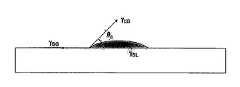
도 3은 막에서 물방울의 접촉각이 어떻게 측정하는지를 보여준다.3 shows how the contact angle of water droplets in the membrane is measured.
도 4는 다양한 O2/HMDSO 가스 유동 비하에 형성된 몇몇 혼성층의 접촉각의 도면을 보여준다.4 shows a plot of the contact angle of several hybrid layers formed under various O2 / HMDSO gas flow ratios.
도 5는 PE-CVD 공정 동안 인가된 다양한 전력 수준하에 형성된 몇몇 혼성층의 접촉각의 도면을 보여준다.5 shows a plot of the contact angle of several hybrid layers formed under various power levels applied during a PE-CVD process.
도 6은 순수한 SiO2(열적 산화물) 또는 순수한 중합체의 막과 비교하여 비교적 높은 O2 유동 및 비교적 낮은 O2 유동을 사용하여 형성된 혼성층의 적외선 흡수 스펙트럼을 보여준다.FIG. 6 shows infrared absorption spectra of hybrid layers formed using relatively high O2 flows and relatively low O2 flows as compared to films of pure SiO2 (thermal oxide) or pure polymers.
도 7은 순수한 SiO2 막의 경도와 비교하여 다양한 O2/HMDSO 가스 유동 비하에 형성된 다양한 혼성층의 나노 압흔 경도의 도면이다.FIG. 7 is a plot of nano indentation hardness of various hybrid layers formed under various O2 / HMDSO gas flow ratios as compared to the hardness of pure SiO2 films.
도 8은 다양한 O2/HMDSO 가스 유동 비하에 형성된 몇몇 혼성층의 표면 조도의 도면이다.8 is a plot of the surface roughness of several hybrid layers formed under various O2 / HMDSO gas flow ratios.
도 9는 다양한 전력 수준하에 형성된 몇몇 혼성층의 표면 조도(toughness)의 도면이다.9 is a diagram of the surface toughness of several hybrid layers formed under various power levels.
도 10a 및 도 10b는 50 ㎛ 두께의 캡톤(Kapton) 폴리이미드 호일 위에 증착된 4 ㎛ 혼성층의 표면의 광학 현미경 사진을 보여준다.10A and 10B show optical micrographs of the surface of a 4 μm hybrid layer deposited on a 50 μm thick Kapton polyimide foil.
도 11은 실시양태에 따른 캡슐화된 OLED의 일부의 단면도를 보여준다.11 shows a cross-sectional view of a portion of an encapsulated OLED according to an embodiment.
도 12는 배리어 코팅을 갖는 완전한 OLED의 가속 환경 시험의 결과를 보여준다.12 shows the results of an accelerated environmental test of a complete OLED with a barrier coating.
도 13은 또 다른 실시양태에 따른 캡슐화된 OLED를 보여준다.13 shows an encapsulated OLED according to another embodiment.
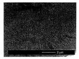
도 14는 또 다른 실시양태에 따른 혼성층의 단면의 주사 전자 현미경 사진을 보여준다.14 shows a scanning electron micrograph of a cross section of a hybrid layer according to another embodiment.
도 15는 또 다른 실시양태에 따른 캡슐화된 OLED를 보여준다.15 shows an encapsulated OLED according to another embodiment.
도 16a 및 도 16b는 또 다른 실시양태에 따른 혼성층의 단면의 주사 전자 현미경 사진을 보여준다.16A and 16B show scanning electron micrographs of cross sections of hybrid layers according to another embodiment.
도 17a는 하나의 설정 조건하에 증착된 혼성층의 단면의 주사 전자 현미경 사진을 보여준다. 도 17b는 또 다른 설정 조건하에 증착된 혼성층의 단면의 주사 전자 현미경 사진을 보여준다.17A shows a scanning electron micrograph of the cross section of the hybrid layer deposited under one set condition. 17B shows a scanning electron micrograph of the cross section of the hybrid layer deposited under another set condition.
도 18a 내지 도 18c는 폴리이미드 기판과 그 위에 증착된 다양한 혼성층 사이의 변형률 불일치의 도면을 보여준다.18A-18C show plots of strain mismatches between polyimide substrates and various hybrid layers deposited thereon.
도 19는 또 다른 실시양태에 따른 캡슐화된 OLED를 보여준다.19 shows an encapsulated OLED according to another embodiment.
도 20은 또 다른 실시양태에 따른 캡슐화된 OLED를 보여준다.20 shows an encapsulated OLED according to another embodiment.
발명의 상세한 설명Detailed description of the invention
하나의 양태에서, 본 발명은 표면 위에 코팅을 형성하는 방법을 제공한다. 상기 방법은 표면 위에 중합체 물질과 비중합체 물질의 혼합물을 포함하는 혼성층을 증착시키는 단계를 포함한다. 혼성층은 단일 상 또는 다중 상을 가질 수 있다.In one embodiment, the present invention provides a method of forming a coating on a surface. The method includes depositing a hybrid layer comprising a mixture of polymeric and non-polymeric materials on a surface. The hybrid layer can have a single phase or multiple phases.
본원에 사용된 용어 "비중합체"는 단일의 매우 한정된 분자량을 갖는 매우 한정된 화학식을 갖는 분자로 제조된 물질을 의미한다. "비중합체" 분자는 상당히 큰 분자량을 가질 수 있다. 몇몇 상황에서, 비중합체 분자는 반복 단위를 포함할 수 있다. 본원에 사용된 용어 "중합체"는 공유 결합된 반복 아단위를 갖고 분자마다 변할 수 있는 분자량을 갖는(이는 중합 반응이 각각의 분자에 대해 상이한 수의 반복 단위를 생성시킬 수 있으므로 그러함) 분자로 제조된 물질을 의미한다. 중합체는 단독중합체 및 공중합체, 예를 들면 블록, 그래프트, 불규칙, 또는 교호 공중합체, 및 이들의 블렌드 및 변형을 포함하지만, 이들에 국한되지는 않는다. 중합체는 탄소 또는 규소의 중합체를 포함하지만, 이들에 국한되지는 않는다.As used herein, the term "nonpolymer" means a material made of a molecule having a very defined formula having a single, very defined molecular weight. "Non-polymer" molecules can have a fairly large molecular weight. In some situations, the nonpolymeric molecule may comprise repeating units. The term "polymer" as used herein is made of molecules having covalently bonded repeating subunits and having a molecular weight that can vary from molecule to molecule, as the polymerization reaction can produce a different number of repeat units for each molecule. Means a substance. Polymers include, but are not limited to, homopolymers and copolymers such as block, graft, irregular, or alternating copolymers, and blends and modifications thereof. Polymers include, but are not limited to, polymers of carbon or silicon.
본원에 사용된 "중합체 물질과 비중합체 물질의 혼합물"은 당해 분야의 숙련된 당업자가 순수한 중합체가 아니고 순수한 비중합체가 아니라고 이해하는 조성물을 의미한다. 용어 "혼합물"은 (예를 들면, 물론 중합체 물질의 열극에 존재할 수 있는) 부수적인 양의 비중합체 물질을 함유하지만, 그럼에도 불구하고 당해 분야의 숙련된 당업자가 순수한 중합체인 것으로 생각하는 임의의 중합체 물질을 배제하도록 의도된다. 마찬가지로, 용어 "혼합물"은 부수적인 양의 중합체 물질을 함유하지만, 그럼에도 불구하고 당해 분야의 숙련된 당업자가 순수한 비중합체인 것으로 생각하는 임의의 비중합체 물질을 배제하도록 의도된다. 몇몇 경우에, 혼성층 내의 중합체 물질 대 비중합체 물질의 중량비는 95:5 대 5:95 범위, 바람직하게는 90:10 내지 10:90 범위, 보다 바람직하게는 25:75 내지 10:90 범위이다.As used herein, "mixture of polymeric and non-polymeric materials" means compositions that are understood by those skilled in the art to be not pure polymers and not pure nonpolymers. The term "mixture" contains any amount of non-polymeric material (eg, which may of course be present in the thermode of the polymeric material), but nevertheless any polymer which a person skilled in the art considers to be a pure polymer It is intended to exclude substances. Likewise, the term “mixture” contains an additional amount of polymeric material, but is nevertheless intended to exclude any non-polymeric material that would be considered purely non-polymeric by those skilled in the art. In some cases, the weight ratio of polymeric material to nonpolymeric material in the hybrid layer is in the range of 95: 5 to 5:95, preferably in the range of 90:10 to 10:90, more preferably in the range of 25:75 to 10:90. .
층의 중합체/비중합체 조성물은 물방울의 습윤 접촉각, IR 흡수, 경도 및 가요성을 비롯한 다양한 기술을 사용하여 측정할 수 있다. 특정한 경우에, 혼성층은 30° 내지 85° 범위, 바람직하게는 30° 내지 60° 범위, 보다 바람직하게는 36° 내지 60° 범위의 습윤 접촉각을 갖는다. 습윤 접촉각은 증착된 그대로의 막의 표면에서 측정할 때의 조성의 측정치임에 유의해야 한다. 습윤 접촉각은 증착후 처리에 의해 크게 변할 수 있으므로, 이러한 처리 후에 이루어진 측정은 층의 조성을 정확히 반영할 수 없다. 이러한 습윤 접촉각은 유기규소 전구체로부터 형성된 다양한 범위의 층에 이용가능한 것으로 생각된다. 특정한 경우에, 혼성층은 3 내지 20 GPa 범위, 바람직하게는 10 내지 18 GPa 범위의 나노 압흔 경도를 갖는다. 특정한 경우에, 혼성층은 0.1 ㎚ 내지 10 ㎚ 범위, 바람직하게는 0.2 ㎚ 내지 0.35 ㎚ 범위의 표면 조도(평균제곱근)를 갖는다. 특정한 경우에, 혼성층은, 50 ㎛ 두께의 폴리이미드 호일 기판 위에 4 ㎛ 두께의 층으로서 증착될 때, 마이크로구조 변화가 0.2%의 인장 변형률(ε)에서 1 인치 직경 롤에서의 55,000회 이상의 회전 주기 후에 관찰되지 않도록 충분히 가요성이다. 특정한 경우에, 혼성층은 크랙이 (당해 분야의 숙련된 당업자가 통상적으로 4 ㎛의 순수한 산화규소 층을 크랙시킨다고 생각하는 인장 변형률 수준인) 0.35% 이상의 인장 변형률(ε) 하에 나타나지 않도록 충분히 가요성이다.The polymeric / non-polymeric composition of the layer can be measured using various techniques including the wet contact angle, IR absorption, hardness and flexibility of the droplets. In certain cases, the hybrid layer has a wet contact angle in the range of 30 ° to 85 °, preferably in the range of 30 ° to 60 °, more preferably in the range of 36 ° to 60 °. It should be noted that the wet contact angle is a measure of the composition as measured on the surface of the film as it is deposited. Since the wet contact angle can vary greatly by the post deposition treatment, the measurements made after this treatment cannot accurately reflect the composition of the layer. Such wet contact angles are believed to be available for a wide range of layers formed from organosilicon precursors. In certain cases, the hybrid layer has a nano indentation hardness in the range of 3 to 20 GPa, preferably in the range of 10 to 18 GPa. In certain cases, the hybrid layer has a surface roughness (average square root) in the range of 0.1 nm to 10 nm, preferably in the range of 0.2 nm to 0.35 nm. In certain cases, when the hybrid layer is deposited as a 4 μm thick layer on a 50 μm thick polyimide foil substrate, the microstructure change is at least 55,000 revolutions in a 1 inch diameter roll at a tensile strain of 0.2% ε. It is flexible enough not to be observed after a cycle. In certain cases, the hybrid layer is sufficiently flexible so that cracks do not appear under a tensile strain (ε) of 0.35% or more (which is the level of tensile strain that a person skilled in the art would typically crack a 4 μm pure silicon oxide layer). to be.
용어 "혼합물"은 단일 상을 갖는 조성물 및 다중 상을 갖는 조성물을 포함하도록 의도된다. 따라서, "혼합물"은 후속적으로 증착된, 교대하는 중합체 층 및 비중합체 층을 배제한다. "혼합물"로 생각되는 또 다른 방식을 고려하면, 층은 동일한 반응 조건하에 및/또는 동시에 증착되어야 한다.The term "mixture" is intended to include compositions having a single phase and compositions having multiple phases. Thus, "mixture" excludes subsequently deposited alternating polymeric and non-polymeric layers. Considering another way of thinking of "mixture", the layers must be deposited under the same reaction conditions and / or simultaneously.
혼성층은 전구체 물질의 단일의 공급원을 화학 증기 증착에 의해 사용하여 형성한다. 본원에 사용된 "전구체 물질의 단일의 공급원"은, 전구체 물질이 반응물 가스의 존재하에 또는 부재하에 CVD에 의해 증착될 때, 중합체 및 비중합체 물질 둘 다를 형성하는데 필요한 전구체 물질 모두를 제공하는 공급원을 의미한다. 이는 중합체 물질이 하나의 전구체 물질을 사용하여 형성되고, 비중합체 물질이 상이한 전구체 물질을 사용하여 형성되는 방법을 배제하고자 의도된다. 전구체 물질의 단일의 공급원을 사용함으로써, 증착 공정은 단순화된다. 예를 들면, 전구체 물질의 단일의 공급원은 전구체 물질의 별개의 스트림의 필요성 및 별개의 스트림을 공급하고 제어하기 위한 부수적인 필요성을 불필요하게 한다.The hybrid layer is formed using chemical vapor deposition using a single source of precursor material. As used herein, a "single source of precursor material" refers to a source that provides both the precursor material needed to form both polymeric and non-polymeric materials when the precursor material is deposited by CVD in the presence or absence of a reactant gas. it means. This is intended to exclude how the polymeric material is formed using one precursor material and the nonpolymeric material is formed using different precursor materials. By using a single source of precursor material, the deposition process is simplified. For example, a single source of precursor material obviates the need for a separate stream of precursor material and an additional need for feeding and controlling the separate stream.
전구체 물질은 단일의 화합물 또는 화합물들의 혼합물일 수 있다. 전구체 물질이 화합물들의 혼합물인 경우, 몇몇 경우에, 혼합물 내의 상이한 화합물 각각은 그 자체로 독립적으로 전구체 물질로서 작용할 수 있다. 예를 들면, 전구체 물질은 헥사메틸 디실록산(HMDSO)과 디메틸 실록산(DMSO)의 혼합물일 수 있다.The precursor material may be a single compound or a mixture of compounds. If the precursor material is a mixture of compounds, in some cases, each of the different compounds in the mixture may itself independently act as precursor material. For example, the precursor material may be a mixture of hexamethyl disiloxane (HMDSO) and dimethyl siloxane (DMSO).
몇몇 경우에, 플라즈마 강화형 CVD(PE-CVD)는 혼성층의 증착에 사용할 수 있다. PE-CVD는 저온 증착, 균일한 코팅 형성, 및 제어가능한 공정 매개변수를 비롯한 다양한 이유로 바람직할 수 있다. 플라즈마를 발생시키는 RF 에너지를 사용하는 공정을 비롯하여 본 발명에서 사용하기에 적합한 다양한 PE-CVD 공정은 당해 분야에 공지되어 있다.In some cases, plasma enhanced CVD (PE-CVD) can be used for the deposition of hybrid layers. PE-CVD may be desirable for a variety of reasons, including low temperature deposition, uniform coating formation, and controllable process parameters. Various PE-CVD processes suitable for use in the present invention, including those using RF energy to generate a plasma, are known in the art.
전구체 물질은 화학 증기 증착에 의해 증착될 때 중합체 물질 및 비중합체 물질 둘 다를 형성할 수 있는 물질이다. 이러한 다양한 전구체 물질은 본 발명에 사용하기에 적합하고 이의 다양한 특성에 대해 선택된다. 예를 들면, 전구체 물질은 이의 화학 원소 함량, 이의 화학 원소의 화학량론적 비 및/또는 CVD하에 형성되는 중합체 및 비중합체 물질에 대해 선택될 수 있다. 예를 들면, 유기규소 화합물, 예컨대 실록산은 전구체 물질로서 사용하기에 적합한 화합물의 유형이다. 실록산 화합물의 대표적인 예로는 헥사메틸 디실록산(HMDSO) 및 디메틸 실록산(DMSO)을 포함한다. CVD에 의해 증착될 때, 이러한 실록산 화합물은 중합체 물질, 예컨대 실리콘 중합체, 및 비중합체 물질, 예컨대 산화규소를 형성할 수 있다. 또한, 전구체 물질은 다양한 다른 특성, 예컨대 비용, 비독성, 취급 특성, 실온에서 액상을 유지하는 능력, 휘발성, 분자량 등에 대해 선택될 수 있다.Precursor materials are materials that can form both polymeric and non-polymeric materials when deposited by chemical vapor deposition. These various precursor materials are suitable for use in the present invention and are selected for their various properties. For example, the precursor material may be selected for its chemical element content, stoichiometric ratio of its chemical element and / or polymer and nonpolymeric materials formed under CVD. For example, organosilicon compounds, such as siloxanes, are a type of compound suitable for use as precursor material. Representative examples of siloxane compounds include hexamethyl disiloxane (HMDSO) and dimethyl siloxane (DMSO). When deposited by CVD, these siloxane compounds can form polymeric materials, such as silicone polymers, and nonpolymeric materials, such as silicon oxide. In addition, the precursor material can be selected for a variety of other properties such as cost, non-toxicity, handling properties, ability to maintain liquid phase at room temperature, volatility, molecular weight and the like.
전구체 물질로서 사용하기에 적합한 다른 유기규소 화합물로는 메틸실란; 디메틸실란; 비닐 트리메틸실란; 트리메틸실란; 테트라메틸실란; 에틸실란; 디실라노메탄; 비스(메틸실라노)메탄; 1,2-디실라노에탄; 1,2-비스(메틸실라노)에탄; 2,2-디실라노프로판; l,3,5-트리실라노-2,4,6-트리메틸렌, 및 이러한 화합물들의 불화 유도체를 포함한다. 전구체 물질로서 사용하기에 적합한 페닐 함유 유기규소 화합물로는 디메틸페닐실란 및 디페닐메틸실란을 포함한다. 전구체 물질로서 사용하기에 적합한 산소 함유 유기규소 화합물로는 디메틸디메톡시실란; 1,3,5,7-테트라메틸사이클로테트라실록산; 1,3-디메틸디실록산; 1,1,3,3-테트라메틸디실록산; 1,3-비스(실라노메틸렌)디실록산; 비스(1-메틸디실록사닐)메탄; 2,2-비스(1-메틸디실록사닐)프로판; 2,4,6,8-테트라메틸사이클로테트라실록산; 옥타메틸사이클로테트라실록산; 2,4,6,8,10-펜타메틸사이클로펜타실록산; 1,3,5,7-테트라실라노-2,6-디옥시-4,8-디메틸렌; 헥사메틸사이클로트리실록산; 1,3,5,7,9-펜타메틸사이클로펜타실록산; 헥사메톡시디실록산, 및 이러한 화합물들의 불화 유도체를 포함한다. 전구체 물질로서 사용하기에 적합한 질소 함유 유기규소 화합물로는 헥사메틸디실라잔; 디비닐테트라메틸디실라잔; 헥사메틸사이클로트리실라잔; 디메틸비스(N-메틸아세트아미도)실란; 디메틸비스-(N-에틸아세트아미도)실란; 메틸비닐비스(N-메틸아세트아미도)실란; 메틸비닐비스(N-부틸아세트아미도)실란; 메틸트리스(N-페닐아세트아미도)실란; 비닐트리스(N-에틸아세트아미도)실란; 테트라키스(N-메틸아세트아미도)실란; 디페닐비스(디에틸아미녹시)실란; 메틸트리스(디에틸아미녹시)실란; 및 비스(트리메틸실릴)카르보디이미드를 포함한다.Other organosilicon compounds suitable for use as precursor materials include methylsilane; Dimethylsilane; Vinyl trimethylsilane; Trimethylsilane; Tetramethylsilane; Ethylsilane; Disilanomethane; Bis (methylsilano) methane; 1,2-disilanoethane; 1,2-bis (methylsilano) ethane; 2,2-disilanopropane; 1,3,5-trisilano-2,4,6-trimethylene, and fluorinated derivatives of these compounds. Suitable phenyl containing organosilicon compounds for use as precursor materials include dimethylphenylsilane and diphenylmethylsilane. Suitable oxygen-containing organosilicon compounds for use as precursor materials include dimethyldimethoxysilane; 1,3,5,7-tetramethylcyclotetrasiloxane; 1,3-dimethyldisiloxane; 1,1,3,3-tetramethyldisiloxane; 1,3-bis (silanomethylene) disiloxane; Bis (1-methyldisiloxanyl) methane; 2,2-bis (1-methyldisiloxanyl) propane; 2,4,6,8-tetramethylcyclotetrasiloxane; Octamethylcyclotetrasiloxane; 2,4,6,8,10-pentamethylcyclopentasiloxane; 1,3,5,7-tetrasilano-2,6-dioxy-4,8-dimethylene; Hexamethylcyclotrisiloxane; 1,3,5,7,9-pentamethylcyclopentasiloxane; Hexamethoxydisiloxane, and fluorinated derivatives of these compounds. Suitable nitrogen-containing organosilicon compounds for use as precursor materials include hexamethyldisilazane; Divinyltetramethyldisilazane; Hexamethylcyclotrisilazane; Dimethylbis (N-methylacetamido) silane; Dimethylbis- (N-ethylacetamido) silane; Methylvinylbis (N-methylacetamido) silane; Methylvinylbis (N-butylacetamido) silane; Methyltris (N-phenylacetamido) silane; Vinyl tris (N-ethylacetamido) silane; Tetrakis (N-methylacetamido) silane; Diphenylbis (diethylaminooxy) silane; Methyltris (diethylaminooxy) silane; And bis (trimethylsilyl) carbodiimide.
CVD에 의해 증착될 때, 전구체 물질은 전구체 물질의 유형, 임의의 반응물 가스의 존재, 및 다른 반응 조건에 따라 다양한 유형의 중합체 물질을 다양한 양으로 형성할 수 있다. 중합체 물질은 무기물 또는 유기물일 수 있다. 예를 들면, 유기규소 화합물이 전구체 물질로서 사용될 때, 증착된 혼성층은 폴리실록산, 폴리카르보실란, 및 폴리실란, 및 유기 중합체를 형성하는 Si-O 결합, Si-C 결합, 또는 Si-O-C 결합의 중합체 쇄를 포함할 수 있다.When deposited by CVD, the precursor material may form various types of polymeric material in varying amounts depending on the type of precursor material, the presence of any reactant gases, and other reaction conditions. The polymeric material may be inorganic or organic. For example, when an organosilicon compound is used as the precursor material, the deposited hybrid layer may be polysiloxane, polycarbosilane, and polysilane, and Si-O bonds, Si-C bonds, or Si-OC bonds to form organic polymers. It may include a polymer chain of.
CVD에 의해 증착될 때, 전구체 물질은 전구체 물질의 유형, 임의의 반응물 가스의 존재, 및 다른 반응 조건에 따라 다양한 유형의 비중합체 물질을 다양한 양으로 형성할 수 있다. 비중합체 물질은 무기물 또는 유기물일 수 있다. 예를 들면, 유기규소 화합물이 산소 함유 반응물 가스와 조합하여 전구체 물질로서 사용될 때, 비중합체 물질은 규소 산화물, 예컨대 SiO, SiO2, 및 혼합 원자가 산화물 SiOx를 포함할 수 있다. 질소 함유 반응물 가스로 증착될 때, 비중합체 물질은 규소 질화물(SiNx)을 포함할 수 있다. 형성될 수 있는 다른 비중합체 물질은 옥시탄화규소 및 옥시질화규소를 포함한다.When deposited by CVD, the precursor material may form various types of nonpolymeric materials in varying amounts depending on the type of precursor material, the presence of any reactant gases, and other reaction conditions. Non-polymeric materials may be inorganic or organic. For example, when an organosilicon compound is used as a precursor material in combination with an oxygen containing reactant gas, the nonpolymeric material may include silicon oxides such as SiO, SiO2 , and mixed valence oxides SiOx . When deposited with a nitrogen containing reactant gas, the non-polymeric material may comprise silicon nitride (SiNx ). Other nonpolymeric materials that may be formed include silicon oxycarbide and silicon oxynitride.
PE-CVD를 사용할 때, 전구체 물질은 PE-CVD 공정에서 전구체 물질과 반응하는 반응물 가스와 조합하여 사용할 수 있다. PE-CVD에서 반응물 가스의 사용은 당해 분야에 공지되어 있고 산소 함유 가스(예, O2, 오존, 물) 및 질소 함유 가스(예, 암모니아)를 비롯한 다양한 반응물 가스가 본 발명에서 사용하기에 적합하다. 반응물 가스는 반응 혼합물에 존재하는 화학 원소의 화학량론적 비를 변화시키기 위해 사용할 수 있다. 예를 들면, 실록산 전구체 물질이 산소 또는 질소 함유 반응물 가스와 함께 사용될 때, 반응물 가스는 반응 혼합물에서 규소 및 탄소에 대해 산소 또는 질소의 화학량론적 비를 변화시킨다. 반응 혼합물에서 다양한 화학 원소들(예, 규소, 탄소, 산소, 질소) 사이의 이러한 화학량론적 관계는 몇몇 방식에서 변할 수 있다. 하나의 방식은 반응에서 전구체 물질 또는 반응물 가스의 농도를 변화시키는 것이다. 또 다른 방식은 반응으로의 전구체 물질 또는 반응물 가스의 유속을 변화시키는 것이다. 또 다른 방식은 반응에서 사용된 전구체 물질 또는 반응물 가스의 유형을 변화시키는 것이다.When using PE-CVD, the precursor material may be used in combination with reactant gases that react with the precursor material in the PE-CVD process. The use of reactant gases in PE-CVD is known in the art and various reactant gases are suitable for use in the present invention, including oxygen containing gases (eg O2 , ozone, water) and nitrogen containing gases (eg ammonia). Do. Reactant gases can be used to change the stoichiometric ratios of the chemical elements present in the reaction mixture. For example, when a siloxane precursor material is used with an oxygen or nitrogen containing reactant gas, the reactant gas changes the stoichiometric ratio of oxygen or nitrogen to silicon and carbon in the reaction mixture. This stoichiometric relationship between various chemical elements (eg, silicon, carbon, oxygen, nitrogen) in the reaction mixture can change in some way. One way is to change the concentration of precursor material or reactant gas in the reaction. Another way is to change the flow rate of precursor material or reactant gas into the reaction. Another way is to change the type of precursor material or reactant gas used in the reaction.
반응 혼합물 내의 원소의 화학량론적 비를 변화시키는 것은 증착된 혼성층 내의 중합체 물질 및 비중합체 물질의 특성 및 상대량에 영향을 미칠 수 있다. 예를 들면, 실록산 가스는 변화하는 양의 산소와 조합되어 혼성층 내의 중합체 물질에 대한 비중합체 물질의 양을 조정할 수 있다. 규소 또는 탄소에 대해 산소의 화학량론적 비를 증가시킴으로써, 비중합체 물질, 예컨대 규소 산화물의 양을 증가시킬 수 있다. 유사하게, 산소의 화학량론적 비를 감소시킴으로써, 규소 및 탄소 함유 중합체 물질의 양을 증가시킬 수 있다. 또한, 혼성층의 조성은 다른 반응 조건을 조정함으로써 변화시킬 수 있다. 예를 들면, PE-CVD의 경우에, 공정 매개변수, 예컨대 RF 전력 및 주파수, 증착 압력, 증착 시간, 및 가스 유속을 변화시킬 수 있다.Changing the stoichiometric ratios of the elements in the reaction mixture can affect the properties and relative amounts of polymeric and non-polymeric materials in the deposited hybrid layer. For example, the siloxane gas can be combined with varying amounts of oxygen to adjust the amount of nonpolymeric material relative to the polymeric material in the hybrid layer. By increasing the stoichiometric ratio of oxygen relative to silicon or carbon, it is possible to increase the amount of nonpolymeric material, such as silicon oxide. Similarly, by reducing the stoichiometric ratio of oxygen, it is possible to increase the amount of silicon and carbon containing polymeric material. In addition, the composition of the hybrid layer can be changed by adjusting other reaction conditions. For example, in the case of PE-CVD, process parameters such as RF power and frequency, deposition pressure, deposition time, and gas flow rate can be varied.
따라서, 본 발명의 방법을 사용함으로써, 혼성 중합체/비중합체 특성 및 다양한 이용분야에서 사용하기에 적합한 특성을 갖는 혼성층을 형성할 수 있다. 이러한 특성으로는 광 투명성(예, 몇몇 경우에, 혼성층은 광 투명함), 불투과성, 가요성, 두께, 접착력, 및 다른 기계적 특성을 포함한다. 예를 들면, 이러한 특성 중 하나 이상은 혼성층 내의 중합체 물질의 중량%를 변화시킴으로써(나머지는 비중합체 물질임) 조정할 수 있다. 예를 들면, 원하는 수준의 가요성 및 불투과성을 달성하기 위해, 중합체 물질 중량%는 바람직하게는 5 내지 95% 범위, 보다 바람직하게는 10 내지 25% 범위일 수 있다. 그러나, 다른 범위도 이용분야에 따라 가능한다.Thus, by using the method of the present invention, it is possible to form hybrid layers having interpolymer / nonpolymeric properties and properties suitable for use in various applications. Such properties include light transparency (eg, in some cases, hybrid layers are light transparent), opaque, flexible, thickness, adhesion, and other mechanical properties. For example, one or more of these properties can be adjusted by varying the weight percent of polymeric material in the hybrid layer (the rest are nonpolymeric materials). For example, to achieve the desired level of flexibility and impermeability, the weight percent polymer material may preferably range from 5 to 95%, more preferably from 10 to 25%. However, other ranges are possible depending on the application.
순수한 비중합체 물질, 예를 들면 산화규소로 제조된 배리어 층은 광학 투명성, 우수한 접착력, 및 우수한 막 응력과 관련된 다양한 이점을 가질 수 있다. 그러나, 이러한 비중합체 층은 층을 통한 수증기 및 산소의 확산을 허용하는 미세 결함을 갖는 경향이 있다. 약간의 중합체 특성을 비중합체 층에 제공하는 것은 순수한 비중합체 층의 유리한 특성을 상당히 변화시키지 않으면서 층의 투과성을 감소시킬 수 있다. 이론에 구속되고자 의도함이 없이, 본 발명자들은 혼성 중합체/비중합체 특성을 갖는 층이 결함, 특히 마이크로크랙(microcrack)의 크기 및/또는 수를 감소시킴으로써 층의 투과성을 감소시킨다고 믿는다.Barrier layers made of pure nonpolymeric material, such as silicon oxide, can have various advantages associated with optical transparency, good adhesion, and good film stress. However, such nonpolymeric layers tend to have fine defects that allow diffusion of water vapor and oxygen through the layer. Providing some polymeric properties to the nonpolymer layer can reduce the permeability of the layer without significantly changing the beneficial properties of the pure nonpolymer layer. Without wishing to be bound by theory, the inventors believe that a layer having interpolymer / nonpolymeric properties reduces the permeability of the layer by reducing the size and / or number of defects, especially microcracks.
몇몇 경우에, 본 발명의 코팅은 다수의 혼성층을 가질 수 있고, 여기서 각각의 혼성층의 조성은 독립적으로 변할 수 있다. 몇몇 경우에, 하나의 혼성층의 중량% 비는 코팅 내의 또 다른 혼성층과 10 중량% 이상 차이가 난다. 각각의 혼성층의 두께도 독립적으로 변할 수 있다. 상이한 혼성층은 혼성층을 증착시키는데 사용된 반응 조건을 순차적으로 조정함으로써 생성할 수 있다. 예를 들면, PE-CVD 공정에서, 반응 혼합물에 제공되는 반응물 가스의 양은 다중 혼성층을 생성하도록 순차적으로 조정할 수 있고, 각각의 혼성층은 불연속적이고 상이한 조성을 갖는다.In some cases, the coatings of the present invention may have multiple hybrid layers, where the composition of each hybrid layer may vary independently. In some cases, the weight percent ratio of one hybrid layer differs by at least 10 weight percent from another hybrid layer in the coating. The thickness of each hybrid layer can also vary independently. Different hybrid layers can be produced by sequentially adjusting the reaction conditions used to deposit the hybrid layer. For example, in a PE-CVD process, the amount of reactant gas provided to the reaction mixture can be adjusted sequentially to produce multiple hybrid layers, each hybrid layer being discontinuous and having a different composition.
코팅이 그 조성이 하나의 고도로부터 또 다른 고도로 실질적으로 연속적으로 변하는 구역을 가질 때, 이 구역 내의 혼성층은 매우 얇을 수 있고, 심지어 코팅 내의 최소 분자 단위만큼 얇을 수 있다. 예를 들면, 코팅은 중합체 물질 대 비중합체 물질의 중량% 비가 연속적으로 변하는 구역을 가질 수 있다. 연속 변형은 선형(예, 중합체 물질 대 비중합체 물질의 중량% 비는 융기부가 더 높을수록 꾸준히 증가할 수 있음) 또는 비선형(예, 주기적으로 증가하고 감소함)일 수 있다.When the coating has a zone whose composition varies substantially from one altitude to another altitude, the hybrid layer in this zone can be very thin, even as thin as the smallest molecular unit in the coating. For example, the coating can have zones in which the weight percent ratio of polymeric material to nonpolymeric material varies continuously. Continuous deformation may be linear (eg, the weight percent ratio of polymeric material to nonpolymeric material may increase steadily at higher ridges) or nonlinear (eg, periodically increasing and decreasing).
혼성층은 다양한 유형의 물품 위에 증착될 수 있다. 몇몇 경우에, 상기 물품은 유기 전자 장치, 예컨대 OLED일 수 있다. OLED의 경우, 혼성층은 수증기 및 산소의 침투에 대항하는 배리어 코팅으로서 작용할 수 있다. 예를 들면, 10-6 g/m2/day 미만의 수증기 투과율 및/또는 10-3 g/m2/day 미만의 산소 투과 속도를 갖는 혼성층은 OLED를 보호하기에 적합할 수 있다. 몇몇 경우에, 혼성층의 두께는 0.1 내지 10 ㎛ 범위일 수 있지만, 다른 두께도 이용분야에 따라 사용할 수 있다. 또한, 광 투명성을 부여하는 두께 및 물질 조성을 갖는 혼성층은 OLED에 사용하기에 적합할 수 있다. 가요성 OLED에 사용하기 위해, 혼성층은 원하는 양의 가요성을 갖도록 설계할 수 있다. 몇몇 경우에, 혼성층은 환경, 예를 들면 의약품, 의학 장치, 생물학적 제제, 생물학적 샘플, 바이오센서, 또는 민감성 측정 장치에 노출시 열화에 민감한 다른 물품에 사용할 수 있다.Hybrid layers may be deposited over various types of articles. In some cases, the article may be an organic electronic device, such as an OLED. In the case of OLEDs, the hybrid layer can act as a barrier coating against the penetration of water vapor and oxygen. For example, hybrid layers having a water vapor transmission rate of less than 10−6 g / m2 / day and / or an oxygen transmission rate of less than 10−3 g / m2 / day may be suitable for protecting the OLED. In some cases, the thickness of the hybrid layer may range from 0.1 to 10 μm, although other thicknesses may be used depending on the application. In addition, hybrid layers having a thickness and material composition that confer light transparency may be suitable for use in OLEDs. For use in flexible OLEDs, the hybrid layer can be designed to have the desired amount of flexibility. In some cases, the hybrid layer can be used in environments such as pharmaceuticals, medical devices, biological agents, biological samples, biosensors, or other articles sensitive to degradation upon exposure to sensitivity measurement devices.
몇몇 경우에, 혼성층은 전구체 물질의 동일한 단일의 공급원, 예를 들면 비혼합된 중합체 층 또는 비혼합된 비중합체 층을 사용함으로써 형성될 수도 있는 비혼합된 층과의 조합으로 사용할 수 있다. 비혼합된 층은 혼성층이 증착되기 이전에 또는 이후에 증착될 수 있다.In some cases, the hybrid layer can be used in combination with an unmixed layer, which may be formed by using the same single source of precursor material, such as an unmixed polymer layer or an unmixed nonpolymer layer. The unmixed layer can be deposited before or after the hybrid layer is deposited.
임의의 다양한 유형의 CVD 반응기는 본 발명의 방법의 실행에 사용할 수 있다. 하나의 일례로서, 도 1은 본 발명의 몇몇 실시양태의 실행에 사용할 수 있는 PE-CVD 기구(10)를 보여준다. PE-CVD 기구(10)는 반응 챔버(20)를 포함하고, 여기서 전자 장치(30)는 홀더(24) 내로 로딩된다. 반응 챔버(20)는 진공을 함유하도록 설계되고 진공 펌프(70)는 반응 챔버(20)에 연결되어 적절한 압력을 생성시키고/시키거나 유지시칸다. N2 가스 탱크(50)는 퍼징 기구(10)에 N2 가스를 제공한다. 반응 챔버(20)는 반응에 의해 생성된 열을 감소시키도록 냉각 시스템을 추가로 포함할 수 있다.Any of various types of CVD reactors can be used in the practice of the method of the present invention. As one example, FIG. 1 shows a PE-
가스 유동을 취급하기 위해, 기구(10)는 또한 수동 또는 자동 제어하에 있을 수 있는 다양한 유동 제어 매카니즘(예를 들면, 질량 유동 제어기(80), 자동차단(shut-off) 밸브(82), 및 체크 밸브(84))을 포함한다. 전구체 물질 공급원(40)은 기화되어 반응 챔버(20) 내로 공급되는 전구체 물질(예, 액체 형태의 HMDSO)을 제공한다. 몇몇 경우에, 전구체 물질은 아르곤과 같은 캐리어 가스를 사용하여 반응 챔버(20)로 이동될 수 있다. 반응물 가스 탱크(60)는 반응물 가스(예, 산소)를 제공하고, 이 반응물 가스는 또한 반응 챔버(20) 내로 공급된다. 전구체 물질 및 반응물 가스는 반응 챔버(20) 내로 유동하여 반응 혼합물(42)을 생성시킨다. 반응 챔버(20) 내부의 압력은 추가로 조정하여 증착 압력을 달성할 수 있다. 반응 챔버(20)는 도체 또는 절연체일 수 있는 전극 격리부(standoff)(26)에 탑재된 일련의 전극(22)을 포함한다. 장치(30) 및 전극(22)의 다양한 배열이 가능하다. 2극관 또는 3극관 전극, 또는 원거리 전극을 사용할 수 있다. 장치(30)는 도 1에 도시된 바대로 원거리에 위치할 수 있거나, 또는 2극관 배치의 하나의 전극 또는 전극 둘 다에 탑재될 수 있다.To handle the gas flow, the
전극(22)에 RF 전력을 공급하여 반응 혼합물(42)에서 플라즈마 조건을 생성시킨다. 플라즈마에 의해 생성된 반응 생성물은 전자 장치(30) 위에 증착시킨다. 반응은 혼성층을 전자 장치(30) 위에 증착시키기에 충분한 시간 기간 동안 진행되도록 허용한다. 반응 시간은 다양한 인자, 예를 들면 전극(22)과 관련하여 장치(30)의 위치, 증착시키고자 하는 혼성층의 유형, 반응 조건, 혼성층의 원하는 두께, 전구체 물질 및 반응물 가스에 의존한다. 반응 시간은 5 초 내지 5 시간 사이의 지속시간일 수 있지만, 더 긴 또는 더 짧은 시간도 이용 분야에 따라 사용할 수 있다.RF power is supplied to the
하기 표 1은 3가지 실시예 혼성층을 만들기 위해 사용된 반응 조건을 보여준다. 실시예 1의 혼성층은, 물방울의 습윤 접촉각으로부터 측정될 때, 대략 7% 중합체 물질 및 93% 비중합체 물질을 함유한다. 실시예 2의 혼성층은, 물방울의 습윤 접촉각으로부터 측정될 때, 대략 94% 중합체 물질 및 6% 비중합체 물질을 함유한다. 실시예 3의 혼성층은, 물방울의 습윤 접촉각으로부터 측정될 때, 대략 25% 중합체 물질 및 75% 비중합체 물질을 함유한다.Table 1 below shows the reaction conditions used to make the three example hybrid layers. The hybrid layer of Example 1 contains approximately 7% polymeric material and 93% nonpolymeric material, as measured from the wet contact angle of water droplets. The hybrid layer of Example 2 contains approximately 94% polymeric material and 6% nonpolymeric material, as measured from the wet contact angle of the water droplets. The hybrid layer of Example 3 contains approximately 25% polymeric material and 75% nonpolymeric material, as measured from the wet contact angle of the water droplets.
도 2는 실시예 3의 혼성층의 광 투과 스펙트럼을 보여준다. 이러한 혼성층은 근자외선 스펙트럼 내지 근적외선 스펙트럼에서 90% 초과의 투과율을 갖는다. 도 3은 막에서 물방울의 접촉각이 어떻게 측정하는지를 보여준다. 도 4는 순수한 SiO2 막 및 순수한 중합체 막의 접촉각과 비교하여 다양한 O2/HMDSO 가스 유동 비하에 형성된 몇몇 혼성층의 접촉각의 도면이다. 혼성층의 접촉각은 증착 공정에서 산소 유속이 증가하면서 순수한 SiO2 막의 접촉각에 근접한다.2 shows the light transmission spectrum of the hybrid layer of Example 3. FIG. Such hybrid layers have a transmittance of greater than 90% in the near ultraviolet spectrum to the near infrared spectrum. 3 shows how the contact angle of water droplets in the membrane is measured. 4 is a plot of the contact angles of several hybrid layers formed under various O2 / HMDSO gas flow ratios as compared to the contact angles of pure SiO2 membranes and pure polymer membranes. The contact angle of the hybrid layer approaches the contact angle of the pure SiO2 film with increasing oxygen flow rate in the deposition process.
도 5는 PE-CVD 공정 동안 인가된 다양한 전력 수준하에 형성된 몇몇 혼성층의 접촉각의 도면이다. 혼성층의 접촉각은 전력 수준이 증가하면서 순수한 SiO2 막의 접촉각에 근접하고, 이는 더 높은 전력 수준이 O2를 더 강한 산화제로 만든다는 사실에 의한 것일 수 있다. 도 6은 순수한 SiO2(열적 산화물) 또는 순수한 중합체의 막과 비교하여 비교적 높은 O2 유동 및 비교적 낮은 O2 유동을 사용하여 형성된 혼성층의 적외선 흡수 스펙트럼을 보여준다. 높은 O2 혼성층은 Si-O-Si 밴드에서 강한 피크를 보여준다. 열적 산화물(순수한 SiO2) 막에 대한 Si-CH3 밴드에서의 공칭 피크는 Si-O 진동과 관련되는 것으로 생각된다. 도 7은 순수한 SiO2 막의 경도와 비교하여 다양한 O2/HMDSO 가스 유동 비하에 형성된 다양한 혼성층의 나노 압흔 경도의 도면이다. 혼성층의 경도는 증착 공정에서 산소 유속이 증가하면서 증가하고, 이러한 혼성층은 경질의 순수한 SiO2 막에 거의 근접할 수 있지만, 여전히 거칠고 고도로 가요성이다.5 is a diagram of the contact angle of several hybrid layers formed under various power levels applied during a PE-CVD process. The contact angle of the hybrid layer approaches the contact angle of the pure SiO2 film with increasing power level, which may be due to the fact that higher power levels make O2 a stronger oxidant. FIG. 6 shows infrared absorption spectra of hybrid layers formed using relatively high O2 flows and relatively low O2 flows as compared to films of pure SiO2 (thermal oxide) or pure polymers. The high O2 hybrid layer shows strong peaks in the Si-O-Si band. The nominal peak in the Si-CH3 band for the thermal oxide (pure SiO2 ) film is believed to be related to the Si-O oscillation. FIG. 7 is a plot of nano indentation hardness of various hybrid layers formed under various O2 / HMDSO gas flow ratios as compared to the hardness of pure SiO2 films. The hardness of the hybrid layer increases with increasing oxygen flow rate in the deposition process, which may be close to a hard, pure SiO2 film, but is still rough and highly flexible.
도 8은 원자 현미경에 의해 측정된, 다양한 02/HMDS0 가스 유동 비하에 형성된 몇몇 혼성층의 표면 조도(평균제곱근)의 도면이고, 표면 조도가 증착 공정에서 사용된 O2 유속이 증가하면서 감소한다는 것을 보여준다. 도 9는 원자 현미경에 의해 측정된, 다양한 전력 수준하에 형성된 몇몇 혼성층의 표면 조도(평균제곱근)의 도면이고, 표면 조도가 증착 공정에서 사용된 전력 수준이 증가하면서 감소한다는 것을 보여준다.FIG. 8 is a plot of the surface roughness (average square root) of several hybrid layers formed under various 02 / HMDS0 gas flow ratios, measured by atomic force microscopy, indicating that surface roughness decreases with increasing O2 flow rate used in the deposition process. Shows that FIG. 9 is a plot of the surface roughness (average square root) of several hybrid layers formed under various power levels, measured by atomic force microscopy, showing that surface roughness decreases with increasing power level used in the deposition process.
도 10a 및 도 10b는 50 ㎛ 두께의 캡톤 폴리이미드 호일 위의 (상기 실시예 3의 동일한 공급원 온도, 가스 유속, 압력 및 RF 전력하에 증착된) 4 ㎛ 혼성층의 표면의 광학 현미경 사진을 보여준다. 도 10a에서, 이미지는 코팅된 호일이 1 인치 직경 롤(인장 변형률 ε = 0.2%)에서 주기적 회전 처리되기 이전에 및 이후에 얻는다. 마이크로구조 변화는 58,600회 회전 주기 후에 관찰되지 않았다. 도 10b에서, 코팅된 호일은 인장 변형률 증가로 처리하고, 이미지는 제1 크래킹(14 ㎜의 롤 직경) 발생 이후에 그리고 광범위한 크래킹(2 ㎜의 롤 직경) 이후에 얻는다. 이러한 가요성 결과는 본 발명의 방법이 매우 가요성인 코팅을 제공할 수 있다는 것을 증명한다.10A and 10B show optical micrographs of the surface of a 4 μm hybrid layer (deposited under the same source temperature, gas flow rate, pressure and RF power of Example 3 above) on a 50 μm thick Kapton polyimide foil. In FIG. 10A, the image is obtained before and after the coated foil is subjected to cyclic rotation on a 1 inch diameter roll (tensile strain ε = 0.2%). No microstructure change was observed after 58,600 rotation cycles. In FIG. 10B, the coated foil is treated with an increase in tensile strain, and images are obtained after the first cracking (roll diameter of 14 mm) and after extensive cracking (roll diameter of 2 mm). This flexible result demonstrates that the method of the present invention can provide a very flexible coating.
도 11은 기판(150) 위의 적절한 OLED(140) 및 배리어 코팅(110)으로서의 상기 실시예 3의 혼성층을 포함하는 캡슐화된 OLED(100)의 일부의 단면도를 보여준다. 도 12는 배리어 코팅을 갖는 완전한 OLED의 가속 환경 시험의 결과를 보여준다. 배면 발광 OLED 및 투명 OLED 둘 다를 실시예 3의 6 ㎛ 두께 혼성층으로 코팅한다. 이어서, 그 장치를 65℃ 및 85% 상대 습도에서 환경 챔버에서 조작한다. 그 이미지는 초기 시점에서 그리고 표시된 시간 간격 이후에 OLED의 상태를 보여준다. OLED는 본 발명의 방법이 환경 노출의 열화 효과에 대해 효과적으로 보호하는 코팅을 제공할 수 있다는 것을 증명하면서 1,000 시간이 쾌 지난 후에 계속해서 기능한다.11 shows a cross-sectional view of a portion of an encapsulated
혼성층을 전자 장치에 대한 환경 배리어로서 사용하는 경우에, 혼성층은 전자 장치가 증착되는 표면으로서, 전자 장치에 대한 커버로서, 또는 둘 다로서 작용할 수 있다. 예를 들면, 하나의 혼성층은 전자 장치 위에 증착되어 전자 장치를 커버할 수 있고, 또 다른 혼성층은 전자 장치 밑의 기판 위에 참착되어 전자 장치가 증착되는 표면을 제공할 수 있다. 이러한 방식으로, 전자 장치는 2개의 혼성층 사이에 밀봉된다.In the case of using the hybrid layer as an environmental barrier for the electronic device, the hybrid layer can act as a surface on which the electronic device is deposited, as a cover for the electronic device, or both. For example, one hybrid layer can be deposited over an electronic device to cover the electronic device, and another hybrid layer can be deposited over the substrate beneath the electronic device to provide a surface on which the electronic device is deposited. In this way, the electronic device is sealed between the two hybrid layers.
예를 들면, 도 13에 도시된 실시양태를 참조하면, 캡슐화된 OLED(160)는 혼성층(162)이 위에 증착된 기판(150)을 포함한다. OLED의 본체(140)(전극 포함)는 혼성층(162)의 표면 위에 배치한다. 또 다른 혼성층(164)(혼성층(162)과 동일한 조성을 갖거나 갖지 않을 수 있음)은 절연보호 코팅(conformal coating)으로서 OLED 본체(140) 위에 증착된다. 그것만으로, OLED 본체(140)의 상부를 커버하는 것 이외에, 혼성층(164)은 또한 OLED 본체(140)의 측면 아래로 연장되고 혼성층(162)의 표면과 접촉한다. 이러한 방식으로, OLED 본체(140)는 혼성층(162)과 혼성층(164) 사이에 스위칭된다.For example, referring to the embodiment shown in FIG. 13, encapsulated
특정 실시양태에서, 혼성층이 증착된 표면은 표면과 혼성층 사이의 계면 응집력을 증가시키기 위해 혼성층을 증착시키기 이전에 전처리할 수 있다. 표면 전처리는 표면의 접착력의 향상, 표면 화학의 개질(예, 표면 활성화), 표면 조도의 변화, 표면 에너지의 증가, 표면의 평탄화 및/또는 표면의 세정을 비롯한 다양한 표면 특성을 개질시킬 수 있다. 표면과 혼성층 사이의 계면 응집력을 증가시킴으로써, 이러한 특징은 혼성층의 에지로부터 환경 오염물(예를 들면, 수분 또는 산소)의 측면 확산을 감소시키는데 유용할 수 있다.In certain embodiments, the surface on which the hybrid layer is deposited may be pretreated prior to depositing the hybrid layer to increase the interfacial cohesion between the surface and the hybrid layer. Surface pretreatment can modify various surface properties including improving the adhesion of the surface, modifying the surface chemistry (eg, surface activation), changing the surface roughness, increasing the surface energy, smoothing the surface, and / or cleaning the surface. By increasing the interfacial cohesion between the surface and the hybrid layer, this feature can be useful to reduce lateral diffusion of environmental contaminants (eg, moisture or oxygen) from the edge of the hybrid layer.
기계적 연마, 화학적 처리(예, 산화제에의 노출, 작용기 도입에 의한 활성화) 또는 물리적-화학적 처리(예, 플라즈마에의 노출, 코로나 방전 또는 UV 조사)를 비롯하여 표면과 혼성층 사이의 계면 응집력을 증가시킬 수 있는 다양한 유형의 표면 처리가 본 발명에서 사용하기에 적합하다. 플라즈마 처리가 사용될 때, 그 처리는 혼성층을 증착시키는데 사용된 동일한 챔버에서 수행할 수 있거나, 또는 플라즈마 처리는 별개의 기구에서 수행할 수 있고, 각각의 경우에, 배럴 유형 플라즈마 시스템 및 병렬판 유형 플라즈마 시스템을 비롯하여 당해 분야에 공지된 다양한 유형의 임의의 플라즈마 처리 기구를 사용할 수 있다.Increase the interfacial cohesion between the surface and the hybrid layer, including mechanical polishing, chemical treatment (eg exposure to oxidants, activation by introduction of functional groups) or physical-chemical treatment (eg exposure to plasma, corona discharge or UV irradiation) Various types of surface treatments that can be made are suitable for use in the present invention. When plasma treatment is used, the treatment may be performed in the same chamber used to deposit the hybrid layer, or the plasma treatment may be performed in a separate instrument, in each case a barrel type plasma system and a parallel plate type. Any plasma processing instrument of various types known in the art, including plasma systems, can be used.
가스, 예를 들면 산소, 수소, 질소, 아르곤, 암모니아, 또는 이들의 혼합물을 비롯하여 플라즈마 처리에서 통상적으로 사용되는 임의의 다양한 가스는 표면을 보호하는데 적합할 수 있다. 특히 바람직한 가스는 산소 및 아르곤을 포함한다. 상이한 가스는 상이한 방식으로 표면을 개질시키기 위해 사용할 수 있다. 예를 들면, 아르곤 가스에 의한 플라즈마 처리는 아르곤 이온에 의해 표면에 충격을 주고, 이는 표면을 세정할 수 있거나 또는 표면을 분자 수준에서 더 거칠게 맒듬으로써, 혼성층에 부착하는 이의 능력을 개선시킨다. 산소에 의한 플라즈마 처리는 화학적으로 산소 함유 작용기를 갖는 표면을 활성화시킬 수 있고, 이는 혼성층과 결합을 형성할 수 있다. 원하는 표면 특성을 달성하기 위해, 전력, 주파수, 지속시간, 압력 또는 온도를 비롯한 플라즈마 처리 공정의 다양한 다른 매개변수를 조정할 수 있다.Gases, such as oxygen, hydrogen, nitrogen, argon, ammonia, or mixtures thereof, can be any suitable gas commonly used in plasma treatment to protect the surface. Particularly preferred gases include oxygen and argon. Different gases can be used to modify the surface in different ways. For example, plasma treatment with argon gas bombards the surface with argon ions, which can clean the surface or roughen the surface at a molecular level, thereby improving its ability to adhere to the hybrid layer. Plasma treatment with oxygen can chemically activate the surface with oxygen-containing functional groups, which can form bonds with the hybrid layer. To achieve the desired surface properties, various other parameters of the plasma treatment process can be adjusted, including power, frequency, duration, pressure or temperature.
몇몇 경우에, 표면은 표면과 혼성층 사이에 개재층을 배치시킴으로써 전처리할 수 있다. 개재층은 표면과 혼성층 사이의 계면 응집력을 개선시키도록 작용할 수 있는 임의의 다양한 물질을 포함한다. 예를 들면, 개재층에 사용하기에 적합한 물질로는 질화규소, 크롬, 티탄, 니켈-티탄 합금, 또는 유전 물질을 포함한다. 이러한 층은 화학 증기 증착, 플라즈마 증기 증착 또는 스퍼터링을 비롯하여 박막의 증착에 통상적으로 사용되는 임의의 다양한 기술을 사용하여 증착시킬 수 있다. 개재층의 두께는 특정한 이용분야에 따라 변한다. 몇몇 경우에, 개재층은 단일 원자 또는 단일 분자 층일 수 있거나, 또는 50 ㎚ 이하의 두께를 가질 수 있지만, 다른 경우에 다른 두께도 가능하다. 개재층에서의 물질은 추가로 개재층 위의 또는 밑의 층 또는 구조물 내의 물질과 화학 반응을 겪을 수 있다.In some cases, the surface may be pretreated by placing an intervening layer between the surface and the hybrid layer. The intervening layer includes any of a variety of materials that can act to improve the interfacial cohesion between the surface and the hybrid layer. For example, suitable materials for use in the intervening layer include silicon nitride, chromium, titanium, nickel-titanium alloys, or dielectric materials. Such layers may be deposited using any of a variety of techniques commonly used for the deposition of thin films, including chemical vapor deposition, plasma vapor deposition, or sputtering. The thickness of the intervening layer varies depending on the particular application. In some cases, the intervening layer may be a single atom or a single molecular layer, or may have a thickness of 50 nm or less, but in other cases other thicknesses are possible. The material in the intervening layer may further undergo chemical reaction with the material in the layer or structure above or below the intervening layer.
도 14는 에칭된 규소 웨이퍼 위에 증착된 혼성층의 단면의 주사 전자 현미경 사진(SEM)을 보여준다. (5 ㎛ 단차 높이를 갖는 융기된 에지로서 도 14의 왼쪽에 도시된) 규소 웨이퍼의 비에칭된 부분은 크롬 80 ㎚ 막으로 커버하고, 이는 또한 규소 웨이퍼의 에칭 동안 에칭 마스크로서 기능한다. (도 14의 오른쪽에 도시된) 규소 웨이퍼의 에칭된 부분은 크롬 막으로 전처리하지 않는다. 혼성층은 다음의 조건하에 규소 웨이퍼의 부분 둘 다에 대해 PE-CVD로 증착시킨다:14 shows a scanning electron micrograph (SEM) of the cross section of the hybrid layer deposited on the etched silicon wafer. The unetched portion of the silicon wafer (shown on the left side of FIG. 14 as a raised edge with 5 μm step height) is covered with a
* 각각 25 분의 2의 간헐적인 기간(각각의 기간 사이에 냉각됨)에서.* In intermittent periods of 2/2 minutes each (cooled between each period).
간헐적인 증착 공정의 가열 및 냉각 주기를 통한 규소 웨이퍼 기판의 평균 온도는 (약 22℃의 출발 온도 및 약 160℃의 종료 온도와 동시에) 80℃ 초과이다. 크롬 처리된 표면 위에, 혼성층은 치밀한 마이크로구조를 갖는다. 그러나, 비처리된 표면 위에, 배리어는 불규칙한 원주형 마이크로구조를 갖는다. 형태학적 차이에 기초하여, (치밀한 마이크로구조를 갖는) 크롬 처리된 표면 위의 혼성층은 비처리된 표면 위에 증착된 혼성층보다 수분 및 산소에 덜 투과성일 것으로 기대될 수 있다.The average temperature of the silicon wafer substrate through the heating and cooling cycles of the intermittent deposition process is above 80 ° C (simultaneously with the starting temperature of about 22 ° C and the ending temperature of about 160 ° C). On the chromed surface, the hybrid layer has a dense microstructure. However, on the untreated surface, the barrier has an irregular columnar microstructure. Based on morphological differences, it can be expected that hybrid layers on chromium treated surfaces (with dense microstructures) are less permeable to moisture and oxygen than hybrid layers deposited on untreated surfaces.
몇몇 경우에, 개재층은 하나 이상의 평탄화 하위층 및 하나 이상의 접착 향상 하위층을 포함하는 다층 구조일 수 있다. 예를 들면, 미국 특허 제6,597,111호(Silvernail et al.) 및 미국 특허 제7,187,119(Weaver)는 교대하는 일련의 중합체 평탄화 하위층 및 고밀도 하위층으로 형성된 배리어를 기재하고 있다. 중합체 평탄화 하위층은 매끄러운 표면을 형성하는 중합체 평탄화 물질을 포함한다. 고밀도 하위층은 환경 오염물의 확산이 방해되도록 충분히 가까운 원자 간격으로 고밀도 물질(예, 무기, 세라믹 또는 유전 물질)을 포함한다. 또 다른 실시예에서, 개재층은 스핀 코팅된 중합체 층 및 (상기 기재된 바대로 증착된) 혼성층; 또는 SiNx 층 및 혼성층; 또는 스핀 코팅된 중합체 층 및 SiNx 층의 교대하는 다층을 포함할 수 있다.In some cases, the intervening layer can be a multi-layered structure that includes one or more planarization sublayers and one or more adhesion enhancement sublayers. For example, US Pat. No. 6,597,111 (Silvernail et al.) And US Pat. No. 7,187,119 (Weaver) describe barriers formed of alternating series of polymer planarization sublayers and high density sublayers. The polymer planarization sublayer includes a polymer planarization material that forms a smooth surface. The high density sublayer contains high density materials (eg, inorganic, ceramic or dielectric materials) at atomic close enough to prevent the spread of environmental contaminants. In another embodiment, the intervening layer comprises a spin coated polymer layer and a hybrid layer (deposited as described above); Or SiNx layers and hybrid layers; Or alternating multilayers of spin coated polymer layers and SiNx layers.
예를 들면, 도 15에 도시된 실시양태를 참조하면, 기판(150)은 중합체 물질의 평탄화 하위층(170)으로 코팅한다. 접착력 향상 하위층(172)은 평탄화 하위층(170) 위에 배치한다. OLED의 본체(140)(전극 포함)는 접착력 향상 하위층(172)의 표면 위에 배치한다. 이어서, 혼성층(174)은 절연보호 코팅으로서 OLED 본체(140) 위에 증착된다. 그것만으로, OLED 본체(140)의 상부를 커버하는 것 이외에, 혼성층(174)은 또한 OLED 본체(140)의 측면 아래로 연장되고 접착력 향상 하위층(172)의 표면과 접촉한다. 이러한 방식으로, 혼성층(174)과 접착력 향상 하위층(172) 사이의 접착은 계면 구역을 통한 환경 오염물의 측면 확산을 감소시킬 수 있다.For example, referring to the embodiment shown in FIG. 15,
상기 설명한 바대로, 증착 조건은 혼성층에 상이한 구조, 조성 및/또는 (환경 오염물에 대한 이의 투과성 및 혼성층이 증착된 표면에 대한 이의 접착력을 비롯한) 특성을 제공하도록 변할 수 있다. 몇몇 경우에, (예, 기판의 가열 및 냉각을 통한) 증착 온도는 혼성층의 투과성을 감소시키도록 제어할 수 있다. 도 16a 및 도 16b는 에칭된 규소 웨이퍼 위에 증착된 혼성층의 단면의 주사 전자 현미경 사진(SEM)을 보여준다. (융기된 에지로서 도 16a 및 도 16b의 오른쪽에 도시된) 규소 웨이퍼의 비에칭된 부분은 크롬의 박막으로 커버하고, 이는 또한 규소 웨이퍼의 에칭 동안 에칭 마스크로서 기능한다. (도 16a 및 도 16b의 왼쪽에 도시된) 규소 웨이퍼의 에칭된 부분은 크롬 박막으로 전처리하지 않는다. 혼성층은 다음의 조건하에 규소 웨이퍼의 부분 둘 다에 대해 PE-CVD로 증착시킨다:As discussed above, the deposition conditions can be varied to provide the hybrid layer with different structures, compositions and / or properties (including its permeability to environmental contaminants and its adhesion to the surface on which the hybrid layer is deposited). In some cases, the deposition temperature (eg, through heating and cooling of the substrate) can be controlled to reduce the permeability of the hybrid layer. 16A and 16B show scanning electron micrographs (SEM) of cross sections of hybrid layers deposited on etched silicon wafers. The unetched portions of the silicon wafer (shown to the right of FIGS. 16A and 16B as raised edges) are covered with a thin film of chromium, which also functions as an etch mask during etching of the silicon wafer. The etched portions of the silicon wafer (shown on the left side of FIGS. 16A and 16B) are not pretreated with a chromium thin film. The hybrid layer is deposited by PE-CVD on both portions of the silicon wafer under the following conditions:
* 각각 5 분의 16의 간헐적인 기간(각각의 기간 사이에 냉각됨)에서.* In intermittent periods of 16 of 5 minutes each (cooled between each period).
간헐적인 증착 공정의 가열 및 냉각 주기를 통한 규소 웨이퍼 기판의 평균 온도는 35℃ 이상이다. 간헐적인 증착 공정에서, 증착 온도를 제어하는 하나의 방식은 가열 및/또는 주기의 수 또는 기간을 조정하는 것이다. 그것만으로, 이러한 혼성층은 더 짧은 지속시간의 가열 주기 및 더 많은 수의 냉각 주기로 증착되므로, 평균 증착 온도는 도 14에 도시된 혼성층을 증착시키는데 사용된 온도보다 더 낮다. 결과로서, 규소 웨이퍼의 크롬 처리된 표면 및 비처리된 표면(bare surface) 둘 다 위의 혼성층은 불규칙한 원주형 마이크로구조를 갖는다. 또한, 그 단차의 측면에 대해 빈약한 피복율(coverage)이 존재한다. 따라서, 일정 범위 내의 더 높은 증착 온도를 사용하여 형성된 혼성층은 더 낮은 증착 온도를 사용하여 형성된 혼성층보다 더 낮은 투과성을 가질 것으로 기대될 수 있다. 몇몇 경우에, 혼성층은 40℃ 내지 90℃ 범위의 증착 온도하에 증착된다.The average temperature of the silicon wafer substrate through the heating and cooling cycles of the intermittent deposition process is at least 35 ° C. In an intermittent deposition process, one way of controlling the deposition temperature is to adjust the number or duration of heating and / or cycles. As such, these hybrid layers are deposited with shorter duration heating cycles and larger number of cooling cycles, so that the average deposition temperature is lower than the temperature used to deposit the hybrid layers shown in FIG. As a result, the hybrid layer on both the chromed and bare surfaces of the silicon wafer has irregular columnar microstructures. In addition, there is a poor coverage of the side of the step. Thus, a hybrid layer formed using a higher deposition temperature within a range can be expected to have lower permeability than a hybrid layer formed using a lower deposition temperature. In some cases, the hybrid layer is deposited under a deposition temperature in the range of 40 ° C to 90 ° C.
몇몇 경우에, 증착 전력은 혼성층의 투과성을 감소시키기 위해 제어할 수 있다. 도 17a는 배면 발광 OLED 적층물 위에 증착된 혼성층의 단면도의 주사 전자 현미경 사진(SEM)을 보여준다. 혼성층은 다음의 조건하에 PE-CVD에 의해 증착시킨다:In some cases, deposition power can be controlled to reduce the permeability of the hybrid layer. 17A shows a scanning electron micrograph (SEM) of a cross sectional view of a hybrid layer deposited over a back emitting OLED stack. Hybrid layers are deposited by PE-CVD under the following conditions:
* 100 mTorr에서 9 분, 이어서 100 mTorr에서 8 시간 6 분, 이어서 130 mTorr에서 8 시간, 이어서 150 mTorr에서 10 분, 이어서 125 mTorr에서 9 분, 이어서 150 mTorr에서 7 분, 이어서 125 mTorr에서 8 분, 이어서 150 mTorr에서 10 분, 이어서 125 mTorr에서 8 분, 이어서 125 mTorr에서 9 분의 간헐적인 기간에서.* 9 minutes at 100 mTorr, then 8 hours 6 minutes at 100 mTorr, then 8 hours at 130 mTorr, then 10 minutes at 150 mTorr, then 9 minutes at 125 mTorr, then 7 minutes at 150 mTorr, then 8 minutes at 125 mTorr Followed by an intermittent period of 10 minutes at 150 mTorr, then 8 minutes at 125 mTorr, and then 9 minutes at 125 mTorr.
더 높은 증착 전력은 단량체 분해(fragmentation)를 향상시키는 것으로 생각된다. 따라서, 전력을 24 W 내지 50 W로 점차 감소시킴으로써, 혼성층 내의 각각의 후속적인 스트라튬(stratum)은 더 많은 산화물 유사 특성 및 더 적은 중합체 유사 특성을 취하는 것으로 관찰된다. 도 17a에서, (더 낮은 전력하에 증착된) 표면에 가장 가까운 혼성층의 스트라튬은 다공성의 중합체 유사 마이크로구조를 갖는 반면, (더 높은 전력하에 증착된) 표면으로부터 더 먼 스트라튬은 보다 치밀한 산화물 유사 마이크로 구조를 갖는다.Higher deposition powers are believed to improve monomer fragmentation. Thus, by gradually reducing the power from 24 W to 50 W, each subsequent stratum in the hybrid layer is observed to take on more oxide-like properties and less polymer-like properties. In FIG. 17A, the stratum of the hybrid layer closest to the surface (deposited under lower power) has a porous, polymer-like microstructure, while the stratum further away from the surface (deposited under higher power) is more dense oxide. Have a similar microstructure.
도 17b는 다음의 조건하에 전면 발광 OLED 적층물 위에 PE-CVD에 의해 증착된 또 다른 혼성층의 단면의 주사 전자 현미경 사진(SEM)을 보여준다:FIG. 17B shows a scanning electron micrograph (SEM) of a cross section of another hybrid layer deposited by PE-CVD on a top-emitting OLED stack under the following conditions:
* 각각 10 분의 12의 간헐적인 기간(각각의 기간 사이에 냉각됨)에서.* In intermittent periods of 12/10 each (cooled between each period).
도 17a에 도시된 혼성층과 비교하여, 더 높은 증착 전력은 도 17b에 도시된 혼성층을 증착시키는데 사용된다. 결과로서, 이러한 혼성층은 도 17a에 도시된 혼성층의 마이크로구조보다 더 치밀한 마이크로구조를 갖는다. 따라서, 더 높은 증착 전력을 사용하여 형성된 혼성층은 더 낮은 증착 전력을 사용하여 형성된 혼성층보다 낮은 투과성을 갖는 것으로 기대될 수 있다.In comparison with the hybrid layer shown in FIG. 17A, higher deposition power is used to deposit the hybrid layer shown in FIG. 17B. As a result, this hybrid layer has a denser microstructure than the microstructure of the hybrid layer shown in FIG. 17A. Thus, a hybrid layer formed using higher deposition power can be expected to have lower permeability than a hybrid layer formed using lower deposition power.
2개의 비유사 물질을 또 다른 물질과 밀접하게 접촉시켜 위치시키는 경우, 이러한 접촉은 특히 2의 물질 사이의 계면에서 응력을 생성할 수 있다. 따라서, 몇몇 실시양태에서, 혼성층의 잔류 내부 응력은 혼성층 내의 응력 유도 결함, 예를 들면 크래킹, 보이드(void), 버클링(buckling), 또는 탈라미네이션의 발생을 감소시키도록 제어할 수 있다. 혼성층 내의 내부 응력을 제어하는 하나의 방식은 증착 조건을 조정하는 것이다.When two dissimilar materials are placed in intimate contact with another material, such contact may create stress, especially at the interface between the two materials. Thus, in some embodiments, the residual internal stress of the hybrid layer can be controlled to reduce the occurrence of stress induced defects in the hybrid layer, such as cracking, voids, buckling, or delamination. . One way to control the internal stress in the hybrid layer is to adjust the deposition conditions.
도 18a 내지 도 18c는 25 ㎛ 두께의 캡톤-E 폴리이미드 기판과 상이한 조건하에 위에 증착된 (320 내지 600 ㎚ 두께의) 다양한 혼성층 사이의 변형률 불일치를 보여준다. 양성 불일치는 혼성층 내의 인장 응력에 상응하고 음성 불일치는 혼성층 내의 압축 응력에 상응한다. 도 18a를 참조하면, 증착 전력 및 가스 유속은 일정하게 유지하면서 100 mTorr 내지 150 mTorr의 증착 압력의 증가는 더 높은 인장 응력이 혼성층 내에서 생성되도록 한다. 도 18b를 참조하면, 증착 압력 및 가스 유속은 일정하게 유지하면서 50 W 내지 80 W의 증착 전력의 증가는 더 높은 압축 응력이 혼성층 내에서 생성되도록 한다. 도 18c를 참조하면, 증착 압력 및 전력은 일정하게 유지하면서 1.0/34 내지 2.0/67의 HMDSO/O2 가스 유속의 증가는 더 높은 인장 응력이 혼성층 내에서 생성되도록 한다.18A-18C show strain mismatches between a 25 μm thick Kapton-E polyimide substrate and various hybrid layers (320-600 nm thick) deposited over under different conditions. Positive mismatches correspond to tensile stresses in the hybrid layer and negative mismatches correspond to compressive stresses in the hybrid layer. Referring to FIG. 18A, an increase in deposition pressure of 100 mTorr to 150 mTorr while maintaining deposition power and gas flow rate constant allows higher tensile stress to be generated in the hybrid layer. Referring to FIG. 18B, an increase in deposition power of 50 W to 80 W while maintaining deposition pressure and gas flow rate constant allows higher compressive stress to be produced in the hybrid layer. Referring to FIG. 18C, an increase in HMDSO / O2 gas flow rate of 1.0 / 34 to 2.0 / 67 while maintaining the deposition pressure and power is constant such that higher tensile stresses are generated in the hybrid layer.
이러한 결과는 혼성층 내의 내부 응력은 증착 매개변수를 변화시킴으로써 조정될 수 있다는 것을 나타낸다. 이러한 결과는 또한 혼성층 내의 응력이 최소화될 수 있는 증착 매개변수의 최적의 세트가 존재한다는 것을 나타낸다. 예를 들면, 하나의 증착 매개변수는 혼성층 내의 압축 응력을 생성하도록 조정할 수 있는 반면, 또 다른 증착 매개변수는 혼성층 내의 인장 응력을 일치시키도록 조정할 수 있어서, 0 또는 0에 가까운 잔류 순응력을 생성시킨다. 다층 코팅이 다수의 혼성층을 포함하는 경우, 코팅 내의 전체 응력을 제어하기 위해 각각의 혼성층 내의 응력을 개별적으로 조정할 수도 있다. 예를 들면, 각각의 혼성층은 코팅 내의 전체 응력을 상쇄하도록, 또는 표면으로부터의 거리를 증가시킴으로써 혼성층 내의 응력의 양을 점차 증가시키도록 조정할 수 있다.These results indicate that the internal stress in the hybrid layer can be adjusted by changing the deposition parameters. These results also indicate that there is an optimal set of deposition parameters in which the stress in the hybrid layer can be minimized. For example, one deposition parameter can be adjusted to produce compressive stress in the hybrid layer, while another deposition parameter can be adjusted to match the tensile stress in the hybrid layer, such that residual stiffness close to zero or near zero. Creates. If the multilayer coating comprises multiple hybrid layers, the stresses in each hybrid layer may be individually adjusted to control the overall stress in the coating. For example, each hybrid layer can be adjusted to counteract the total stress in the coating, or to gradually increase the amount of stress in the hybrid layer by increasing the distance from the surface.
전자 장치가 하부구조(즉, 하부구조 표면)로서 제공되는 표면 위에 배치되는 특정 실시양태에서, 혼성층 및/또는 표면은 추가로 하부구조 물질 그 자체를 통한 또는 하부구조 표면과 혼성층 사이의 계면을 통한 측면 확산에 의한 환경 오염물(예, 수분 또는 산소)의 침투를 감소시키기 위해 에지 배리어를 포함할 수 있다. 하부구조는 본원에 기재된 임의의 물질 또는 전자 장치를 위에 배치시키는데 사용하는 것으로 공지된 임의의 다른 물질(예, 금속 호일 기판 또는 배리어 코팅된 플라스틱 기판 위에 평탄화 및/또는 절연 층에 사용된 물질)로 형성할 수 있다. 당해 분야에 공지된 임의의 다양한 유형의 에지 배리어는 본 발명에서 사용하기에 적합하다. 몇몇 경우에, 에지 배리어는 혼성층을 전자 장치에 말단 인접한 구역에서 하부구조 표면에 결합시킴으로써 구조화할 수 있다. 결합은 이러한 구역에 열 밀봉을 인가하거나 또는 접착제(예, 에폭시계 접착제)를 도포함으로써 달성할 수 있다.In certain embodiments in which the electronic device is disposed over a surface provided as an infrastructure (ie, an infrastructure surface), the hybrid layer and / or surface may further be an interface through the infrastructure material itself or between the infrastructure surface and the hybrid layer. Edge barriers may be included to reduce the penetration of environmental contaminants (eg, moisture or oxygen) by lateral diffusion through. The infrastructure may be any material described herein or any other material known to be used to place electronic devices thereon (eg, a material used for planarization and / or insulation layers over metal foil substrates or barrier coated plastic substrates). Can be formed. Any of various types of edge barriers known in the art are suitable for use in the present invention. In some cases, the edge barrier can be structured by bonding the hybrid layer to the substructure surface in the region proximate the electronic device. Bonding can be accomplished by applying a heat seal to this zone or by applying an adhesive (eg, an epoxy based adhesive).
몇몇 경우에, 에지 배리어는 전자 장치의 상부 표면으로부터, 전자 장치의 측면을 따라 아래로, 그리고 하부구조 표면과의 접촉 내로 연장되는 말단 캡일 수 있다. 본 발명에서 사용하기에 적합할 수 있는 말단 캡의 하나의 유형은 미국 제7,002,294호(Forrest et al.)에 기재되어 있다. 말단 캡은 전자 장치를 고밀도 세라믹 물질(예, 이산화규소) 또는 금속 물질을 비롯한 환경 오염물의 측면 내입으로부터 보호할 수 있는 임의의 물질로 제조할 수 있다.In some cases, the edge barrier may be an end cap that extends from the top surface of the electronic device, along the side of the electronic device, and into contact with the underlying structure surface. One type of end cap that may be suitable for use in the present invention is described in US 7,002,294 (Forrest et al.). The end cap can be made of any material that can protect the electronic device from lateral penetration of environmental contaminants, including high density ceramic materials (eg, silicon dioxide) or metal materials.
예를 들면, 도 19에 도시된 실시양태를 참조하면, 캡슐화된 OLED(180)는 OLED의 본체(140)(전극 포함)가 위에 배치된 기판(150)을 포함한다. 혼성층(182)은 OLED 본체(140) 위에 증착된다. 말단 캡(184)은 혼성층(182)의 상부 표면으로부터, OLED 본체(140)의 측면 아래로, 그리고 기판(150)의 표면과의 접촉 내로 연장되도록 혼성층(182) 및 OLED 본체(140) 주위에 배치한다. 말단 캡(184)은 OLED(180)의 측면 표면 또는 에지를 통한 환경 오염물의 측면 내입을 감소시키기기 위해 기능한다.For example, referring to the embodiment shown in FIG. 19, encapsulated
몇몇 경우에, 에지 배리어는 전자 장치에 말단 인접한 구역에서 하부구조 표면 내에 하나 이상의 불연속을 생성함으로써 형성할 수 있다. 이러한 불연속은 환경 오염물의 측면 내입에 대한 경로 길이를 증가시키는 단계, 또는 하부구조 물질이 환경 오염물의 내입에 대한 도관으로서 작용하는 경우, 도관 내의 브레이크를 형성하는 단계를 수반하는 임의의 다양한 매카니즘에 의한 환경 오염물의 침투에 대한 배리어로서 작용할 수 있다. 본원에 사용된 용어 "불연속"은 보이드의 크기, 형태 및 위치를 제어하는 기술을 사용하여 물질의 제거 또는 증착에 의해 하부구조 표면 내에 생성된 분리된 보이드(예, 트렌치, 그루브, 슬랏(slot), 크랙, 브레이크, 갭, 홀, 천공)를 의미한다. 예를 들면, 이러한 기술은 활성 빔(energetic beam)(예를 들면. 레이저, 이온, 또는 전자)을 사용하는 직접쓰기 에칭, 마이크로기계가공(micromachining), 마이크로드릴링(microdrilling), 리소그래피 공정, 또는 보이드가 형성되는 구역에 대한 선택된 마스킹과 함께 하부구조 물질의 마스킹 증착을 포함한다.In some cases, the edge barrier can be formed by creating one or more discontinuities in the substructure surface in a region proximate the electronic device. This discontinuity may be caused by any of the various mechanisms involved in increasing the path length for lateral intrusion of environmental contaminants, or in forming a brake in the conduit if the substructure material acts as a conduit for incorporation of environmental contaminants. It can act as a barrier to the penetration of environmental pollutants. As used herein, the term “discontinuity” refers to discrete voids (eg, trenches, grooves, slots) created within the infrastructure surface by removal or deposition of material using techniques that control the size, shape, and position of the voids. , Cracks, brakes, gaps, holes, perforations). For example, such techniques may be direct write etching, micromachining, microdrilling, lithography processes, or voids using an energetic beam (eg, laser, ion, or electron). Masking deposition of the underlying material with selected masking for the area where is formed.
예를 들면, 도 20에 도시된 실시양태를 참조하면, 기판(150)은 폴리이미드 막(194)으로 코팅한다. 폴리이미드 막(194)은 OLED 본체(140)(전극 포함)가 배치되는 하부구조 표면으로서 직용한다. OLED 본체(140) 주변을 둘러싸는 트렌치(196)는 폴리이미드 막(194) 내로 에칭된다. 대안적으로, 트렌치(196)는 폴리이미드 막(194)의 증착 동안 그 구역을 선택적으로 마스킹함으로써 형성할 수 있다. 트렌치(196)는 폴리이미드 막(194)의 전체 두께를 통해 연장된다. OLED 본체(140)는 혼성층(192)으로 커버하고, 이는 하부구조 표면에 대해, OLED 본체(140)의 측면 아래로 연장될 뿐만 아니라, OLED 본체(194)의 상부를 커버한다. 하부구조 표면에서, 혼성층(192)은 또한 폴리이미드 막이 환경 오염물의 측면 내입을 위한 도관으로서 작용하는 것을 예방하도록 트렌치(196) 내에 채워진다.For example, referring to the embodiment shown in FIG. 20, the
상기의 명세서 및 실시예는 본 발명을 단지 예시하기 위해 기재되어 있으며 제한하도록 의도되지 않는다. 개시된 양태 및 본 발명의 실시양태 각각은 독립적으로 또는 본 발명의 다른 양태, 실시양태 및 변형과 조합되어 고려될 수 있다. 본 발명의 사상 및 물질이 구현되어 있는 개시된 실시양태의 변형은 당해 분야의 숙련된 당업자에게 발생할 수 있고 이러한 변형은 본 발명 범위 내에 있다.The above specification and examples are described for illustrative purposes only and are not intended to be limiting. Each of the disclosed aspects and embodiments of the invention can be considered independently or in combination with other aspects, embodiments, and variations of the invention. Modifications of the disclosed embodiments in which the spirit and materials of the invention are implemented may occur to those skilled in the art and such modifications are within the scope of the invention.
Claims (91)
Translated fromKoreanApplications Claiming Priority (4)
| Application Number | Priority Date | Filing Date | Title |
|---|---|---|---|
| US85604706P | 2006-11-01 | 2006-11-01 | |
| US60/856,047 | 2006-11-01 | ||
| US11/783,361US20080102223A1 (en) | 2006-11-01 | 2007-04-09 | Hybrid layers for use in coatings on electronic devices or other articles |
| US11/783,361 | 2007-04-09 |
Related Child Applications (1)
| Application Number | Title | Priority Date | Filing Date |
|---|---|---|---|
| KR1020157014828ADivisionKR20150084893A (en) | 2006-11-01 | 2007-10-31 | Hybrid layers for use in coatings on electronic devices or other articles |
Publications (1)
| Publication Number | Publication Date |
|---|---|
| KR20090087457Atrue KR20090087457A (en) | 2009-08-17 |
Family
ID=39154140
Family Applications (2)
| Application Number | Title | Priority Date | Filing Date |
|---|---|---|---|
| KR1020097011196ACeasedKR20090087457A (en) | 2006-11-01 | 2007-10-31 | Hybrid Layers for Use on Coatings on Electronic Devices or Other Articles |
| KR1020157014828ACeasedKR20150084893A (en) | 2006-11-01 | 2007-10-31 | Hybrid layers for use in coatings on electronic devices or other articles |
Family Applications After (1)
| Application Number | Title | Priority Date | Filing Date |
|---|---|---|---|
| KR1020157014828ACeasedKR20150084893A (en) | 2006-11-01 | 2007-10-31 | Hybrid layers for use in coatings on electronic devices or other articles |
Country Status (7)
| Country | Link |
|---|---|
| US (1) | US20080102223A1 (en) |
| EP (2) | EP2097555A1 (en) |
| JP (4) | JP5491186B2 (en) |
| KR (2) | KR20090087457A (en) |
| CN (1) | CN103187455B (en) |
| TW (1) | TWI514641B (en) |
| WO (1) | WO2008057394A1 (en) |
Cited By (2)
| Publication number | Priority date | Publication date | Assignee | Title |
|---|---|---|---|---|
| KR20130105521A (en)* | 2012-03-16 | 2013-09-25 | 유니버셜 디스플레이 코포레이션 | Electronic device with reduced non-device edge area |
| KR20200111656A (en)* | 2012-03-16 | 2020-09-29 | 유니버셜 디스플레이 코포레이션 | Edge barrier film for electronic devices |
Families Citing this family (383)
| Publication number | Priority date | Publication date | Assignee | Title |
|---|---|---|---|---|
| US7807275B2 (en) | 2005-04-21 | 2010-10-05 | Universal Display Corporation | Non-blocked phosphorescent OLEDs |
| KR20180117719A (en) | 2006-02-10 | 2018-10-29 | 유니버셜 디스플레이 코포레이션 | METAL COMPLEXES OF CYCLOMETALLATED IMIDAZO[1,2-f]PHENANTHRIDINE AND DIIMIDAZO[1,2-A:1',2'-C]QUINAZOLINE LIGANDS AND ISOELECTRONIC AND BENZANNULATED ANALOGS THEREOF |
| US7825038B2 (en)* | 2006-05-30 | 2010-11-02 | Applied Materials, Inc. | Chemical vapor deposition of high quality flow-like silicon dioxide using a silicon containing precursor and atomic oxygen |
| US7902080B2 (en)* | 2006-05-30 | 2011-03-08 | Applied Materials, Inc. | Deposition-plasma cure cycle process to enhance film quality of silicon dioxide |
| US7790634B2 (en)* | 2006-05-30 | 2010-09-07 | Applied Materials, Inc | Method for depositing and curing low-k films for gapfill and conformal film applications |
| US20070277734A1 (en)* | 2006-05-30 | 2007-12-06 | Applied Materials, Inc. | Process chamber for dielectric gapfill |
| US8232176B2 (en)* | 2006-06-22 | 2012-07-31 | Applied Materials, Inc. | Dielectric deposition and etch back processes for bottom up gapfill |
| US20080102223A1 (en)* | 2006-11-01 | 2008-05-01 | Sigurd Wagner | Hybrid layers for use in coatings on electronic devices or other articles |
| US7745352B2 (en)* | 2007-08-27 | 2010-06-29 | Applied Materials, Inc. | Curing methods for silicon dioxide thin films deposited from alkoxysilane precursor with harp II process |
| US7943531B2 (en)* | 2007-10-22 | 2011-05-17 | Applied Materials, Inc. | Methods for forming a silicon oxide layer over a substrate |
| US7803722B2 (en)* | 2007-10-22 | 2010-09-28 | Applied Materials, Inc | Methods for forming a dielectric layer within trenches |
| US7867923B2 (en)* | 2007-10-22 | 2011-01-11 | Applied Materials, Inc. | High quality silicon oxide films by remote plasma CVD from disilane precursors |
| US8476822B2 (en) | 2007-11-09 | 2013-07-02 | Universal Display Corporation | Saturated color organic light emitting devices |
| KR101833658B1 (en)* | 2008-05-07 | 2018-02-28 | 더 트러스티즈 오브 프린스턴 유니버시티 | Hybrid layers for use in coatings on electronic devices or other articles |
| US8357435B2 (en) | 2008-05-09 | 2013-01-22 | Applied Materials, Inc. | Flowable dielectric equipment and processes |
| US20110068332A1 (en)* | 2008-08-04 | 2011-03-24 | The Trustees Of Princeton University | Hybrid Dielectric Material for Thin Film Transistors |
| KR101880838B1 (en)* | 2008-08-04 | 2018-08-16 | 더 트러스티즈 오브 프린스턴 유니버시티 | Hybrid dielectric material for thin film transistors |
| US20100225252A1 (en) | 2008-10-01 | 2010-09-09 | Universal Display Corporation | Novel amoled display architecture |
| US8980382B2 (en) | 2009-12-02 | 2015-03-17 | Applied Materials, Inc. | Oxygen-doping for non-carbon radical-component CVD films |
| US8741788B2 (en) | 2009-08-06 | 2014-06-03 | Applied Materials, Inc. | Formation of silicon oxide using non-carbon flowable CVD processes |
| US7935643B2 (en)* | 2009-08-06 | 2011-05-03 | Applied Materials, Inc. | Stress management for tensile films |
| US7989365B2 (en)* | 2009-08-18 | 2011-08-02 | Applied Materials, Inc. | Remote plasma source seasoning |
| US20110136347A1 (en)* | 2009-10-21 | 2011-06-09 | Applied Materials, Inc. | Point-of-use silylamine generation |
| US8449942B2 (en) | 2009-11-12 | 2013-05-28 | Applied Materials, Inc. | Methods of curing non-carbon flowable CVD films |
| JP2013516763A (en) | 2009-12-30 | 2013-05-13 | アプライド マテリアルズ インコーポレイテッド | Dielectric film growth using radicals generated using a flexible nitrogen / hydrogen ratio |
| US8329262B2 (en)* | 2010-01-05 | 2012-12-11 | Applied Materials, Inc. | Dielectric film formation using inert gas excitation |
| SG182336A1 (en) | 2010-01-06 | 2012-08-30 | Applied Materials Inc | Flowable dielectric using oxide liner |
| KR101837648B1 (en) | 2010-01-07 | 2018-04-19 | 어플라이드 머티어리얼스, 인코포레이티드 | Insitu ozone cure for radicalcomponent cvd |
| US8288187B2 (en) | 2010-01-20 | 2012-10-16 | Universal Display Corporation | Electroluminescent devices for lighting applications |
| JP2013521650A (en) | 2010-03-05 | 2013-06-10 | アプライド マテリアルズ インコーポレイテッド | Conformal layer by radical component CVD |
| US8236708B2 (en) | 2010-03-09 | 2012-08-07 | Applied Materials, Inc. | Reduced pattern loading using bis(diethylamino)silane (C8H22N2Si) as silicon precursor |
| US7994019B1 (en) | 2010-04-01 | 2011-08-09 | Applied Materials, Inc. | Silicon-ozone CVD with reduced pattern loading using incubation period deposition |
| US8476142B2 (en) | 2010-04-12 | 2013-07-02 | Applied Materials, Inc. | Preferential dielectric gapfill |
| US8524004B2 (en) | 2010-06-16 | 2013-09-03 | Applied Materials, Inc. | Loadlock batch ozone cure |
| US8318584B2 (en) | 2010-07-30 | 2012-11-27 | Applied Materials, Inc. | Oxide-rich liner layer for flowable CVD gapfill |
| US8766240B2 (en) | 2010-09-21 | 2014-07-01 | Universal Display Corporation | Permeation barrier for encapsulation of devices and substrates |
| US9285168B2 (en) | 2010-10-05 | 2016-03-15 | Applied Materials, Inc. | Module for ozone cure and post-cure moisture treatment |
| US8664127B2 (en) | 2010-10-15 | 2014-03-04 | Applied Materials, Inc. | Two silicon-containing precursors for gapfill enhancing dielectric liner |
| US9698140B2 (en) | 2011-01-12 | 2017-07-04 | Universal Display Corporation | OLED lighting device with short tolerant structure |
| US9214510B2 (en) | 2011-01-12 | 2015-12-15 | Universal Display Corporation | OLED lighting device with short tolerant structure |
| US10283321B2 (en) | 2011-01-18 | 2019-05-07 | Applied Materials, Inc. | Semiconductor processing system and methods using capacitively coupled plasma |
| US8450191B2 (en) | 2011-01-24 | 2013-05-28 | Applied Materials, Inc. | Polysilicon films by HDP-CVD |
| US8716154B2 (en) | 2011-03-04 | 2014-05-06 | Applied Materials, Inc. | Reduced pattern loading using silicon oxide multi-layers |
| US8445078B2 (en) | 2011-04-20 | 2013-05-21 | Applied Materials, Inc. | Low temperature silicon oxide conversion |
| WO2012155099A1 (en) | 2011-05-12 | 2012-11-15 | Universal Display Corporation | Flexible lighting devices |
| US8466073B2 (en) | 2011-06-03 | 2013-06-18 | Applied Materials, Inc. | Capping layer for reduced outgassing |
| US9252377B2 (en) | 2011-07-14 | 2016-02-02 | Universal Display Corporation | Inorganic hosts in OLEDs |
| US9404178B2 (en) | 2011-07-15 | 2016-08-02 | Applied Materials, Inc. | Surface treatment and deposition for reduced outgassing |
| US8617989B2 (en) | 2011-09-26 | 2013-12-31 | Applied Materials, Inc. | Liner property improvement |
| WO2013048419A1 (en) | 2011-09-29 | 2013-04-04 | Universal Display Corporation | LAMP WITH MULTIPLE FLEXIBLE OLEDs |
| US8551891B2 (en) | 2011-10-04 | 2013-10-08 | Applied Materials, Inc. | Remote plasma burn-in |
| KR101976104B1 (en) | 2011-11-01 | 2019-05-09 | 유니버셜 디스플레이 코포레이션 | Reducing oled device efficiency at low luminance |
| US8969116B2 (en) | 2012-01-23 | 2015-03-03 | Universal Display Corporation | Selective OLED vapor deposition using electric charges |
| WO2013134661A1 (en)* | 2012-03-09 | 2013-09-12 | Air Products And Chemicals, Inc. | Barrier materials for display devices |
| US20130273239A1 (en) | 2012-03-13 | 2013-10-17 | Universal Display Corporation | Nozzle design for organic vapor jet printing |
| US9386657B2 (en) | 2012-03-15 | 2016-07-05 | Universal Display Corporation | Organic Electroluminescent materials and devices |
| US9054323B2 (en) | 2012-03-15 | 2015-06-09 | Universal Display Corporation | Secondary hole transporting layer with diarylamino-phenyl-carbazole compounds |
| WO2013151095A1 (en)* | 2012-04-05 | 2013-10-10 | シャープ株式会社 | Film formation method and method for manufacturing organic el display device |
| US9741968B2 (en) | 2012-05-30 | 2017-08-22 | Universal Display Corporation | Luminaire and individually replaceable components |
| US9991463B2 (en) | 2012-06-14 | 2018-06-05 | Universal Display Corporation | Electronic devices with improved shelf lives |
| US9210810B2 (en) | 2012-07-12 | 2015-12-08 | Universal Display Corporation | Method of fabricating flexible devices |
| US9246036B2 (en) | 2012-08-20 | 2016-01-26 | Universal Display Corporation | Thin film deposition |
| US8728858B2 (en) | 2012-08-27 | 2014-05-20 | Universal Display Corporation | Multi-nozzle organic vapor jet printing |
| US8889566B2 (en) | 2012-09-11 | 2014-11-18 | Applied Materials, Inc. | Low cost flowable dielectric films |
| US9170665B2 (en) | 2012-09-14 | 2015-10-27 | Universal Display Corporation | Lifetime OLED display |
| US9379169B2 (en) | 2012-09-14 | 2016-06-28 | Universal Display Corporation | Very high resolution AMOLED display |
| US8957579B2 (en) | 2012-09-14 | 2015-02-17 | Universal Display Corporation | Low image sticking OLED display |
| US9412947B2 (en) | 2012-09-14 | 2016-08-09 | Universal Display Corporation | OLED fabrication using laser transfer |
| US9257665B2 (en) | 2012-09-14 | 2016-02-09 | Universal Display Corporation | Lifetime OLED display |
| US10862073B2 (en) | 2012-09-25 | 2020-12-08 | The Trustees Of Princeton University | Barrier film for electronic devices and substrates |
| US9577221B2 (en) | 2012-09-26 | 2017-02-21 | Universal Display Corporation | Three stack hybrid white OLED for enhanced efficiency and lifetime |
| US9252363B2 (en) | 2012-10-04 | 2016-02-02 | Universal Display Corporation | Aryloxyalkylcarboxylate solvent compositions for inkjet printing of organic layers |
| US8764255B2 (en) | 2012-10-10 | 2014-07-01 | Universal Display Corporation | Semi-rigid electronic device with a flexible display |
| US9120290B2 (en) | 2012-10-10 | 2015-09-01 | Universal Display Corporation | Flexible screen backed with rigid ribs |
| US9385340B2 (en) | 2012-10-19 | 2016-07-05 | Universal Display Corporation | Transparent display and illumination device |
| US9384691B2 (en) | 2012-10-19 | 2016-07-05 | Universal Display Corporation | Transparent display and illumination device |
| US9385172B2 (en) | 2012-10-19 | 2016-07-05 | Universal Display Corporation | One-way transparent display |
| US9196860B2 (en) | 2012-12-04 | 2015-11-24 | Universal Display Corporation | Compounds for triplet-triplet annihilation upconversion |
| US8716484B1 (en) | 2012-12-05 | 2014-05-06 | Universal Display Corporation | Hole transporting materials with twisted aryl groups |
| US9653691B2 (en) | 2012-12-12 | 2017-05-16 | Universal Display Corporation | Phosphorescence-sensitizing fluorescence material system |
| US9159945B2 (en) | 2012-12-13 | 2015-10-13 | Universal Display Corporation | System and method for matching electrode resistances in OLED light panels |
| US8766531B1 (en) | 2012-12-14 | 2014-07-01 | Universal Display Corporation | Wearable display |
| US20140166990A1 (en) | 2012-12-17 | 2014-06-19 | Universal Display Corporation | Manufacturing flexible organic electronic devices |
| US8912018B2 (en) | 2012-12-17 | 2014-12-16 | Universal Display Corporation | Manufacturing flexible organic electronic devices |
| US9502681B2 (en) | 2012-12-19 | 2016-11-22 | Universal Display Corporation | System and method for a flexible display encapsulation |
| US10229956B2 (en) | 2013-01-18 | 2019-03-12 | Universal Display Corporation | High resolution low power consumption OLED display with extended lifetime |
| US9424772B2 (en) | 2013-01-18 | 2016-08-23 | Universal Display Corporation | High resolution low power consumption OLED display with extended lifetime |
| US10243023B2 (en) | 2013-01-18 | 2019-03-26 | Universal Display Corporation | Top emission AMOLED displays using two emissive layers |
| US9590017B2 (en) | 2013-01-18 | 2017-03-07 | Universal Display Corporation | High resolution low power consumption OLED display with extended lifetime |
| US10304906B2 (en) | 2013-01-18 | 2019-05-28 | Universal Display Corporation | High resolution low power consumption OLED display with extended lifetime |
| US10580832B2 (en) | 2013-01-18 | 2020-03-03 | Universal Display Corporation | High resolution low power consumption OLED display with extended lifetime |
| US9385168B2 (en) | 2013-01-18 | 2016-07-05 | Universal Display Corporation | High resolution low power consumption OLED display with extended lifetime |
| US9018108B2 (en) | 2013-01-25 | 2015-04-28 | Applied Materials, Inc. | Low shrinkage dielectric films |
| US9252397B2 (en) | 2013-02-07 | 2016-02-02 | Universal Display Corporation | OVJP for printing graded/stepped organic layers |
| US9178184B2 (en) | 2013-02-21 | 2015-11-03 | Universal Display Corporation | Deposition of patterned organic thin films |
| US9000459B2 (en) | 2013-03-12 | 2015-04-07 | Universal Display Corporation | OLED display architecture having some blue subpixel components replaced with non-emissive volume containing via or functional electronic component and method of manufacturing thereof |
| US9018660B2 (en) | 2013-03-25 | 2015-04-28 | Universal Display Corporation | Lighting devices |
| US10514136B2 (en) | 2013-03-25 | 2019-12-24 | Universal Display Corporation | Lighting devices |
| US8979291B2 (en) | 2013-05-07 | 2015-03-17 | Universal Display Corporation | Lighting devices including transparent organic light emitting device light panels and having independent control of direct to indirect light |
| US9865672B2 (en) | 2013-05-15 | 2018-01-09 | Universal Display Corporation | Macro-image OLED lighting system |
| US9484546B2 (en) | 2013-05-15 | 2016-11-01 | Universal Display Corporation | OLED with compact contact design and self-aligned insulators |
| US9041297B2 (en) | 2013-05-20 | 2015-05-26 | Universal Display Corporation | Large area lighting system with wireless control |
| US10468633B2 (en) | 2013-06-05 | 2019-11-05 | Universal Display Corporation | Microlens array architectures for enhanced light outcoupling from an OLED array |
| US9093658B2 (en) | 2013-06-07 | 2015-07-28 | Universal Display Corporation | Pre-stressed flexible OLED |
| US9818967B2 (en) | 2013-06-28 | 2017-11-14 | Universal Display Corporation | Barrier covered microlens films |
| US9823482B2 (en) | 2013-08-19 | 2017-11-21 | Universal Display Corporation | Autostereoscopic displays |
| US9374872B2 (en) | 2013-08-30 | 2016-06-21 | Universal Display Corporation | Intelligent dimming lighting |
| US8981363B1 (en) | 2013-09-03 | 2015-03-17 | Universal Display Corporation | Flexible substrate for OLED device |
| US9496522B2 (en) | 2013-12-13 | 2016-11-15 | Universal Display Corporation | OLED optically coupled to curved substrate |
| US9142778B2 (en) | 2013-11-15 | 2015-09-22 | Universal Display Corporation | High vacuum OLED deposition source and system |
| US9130195B2 (en) | 2013-11-22 | 2015-09-08 | Universal Display Corporation | Structure to enhance light extraction and lifetime of OLED devices |
| US10062738B2 (en) | 2013-11-27 | 2018-08-28 | The Regents Of The University Of Michigan | Devices combining thin film inorganic LEDs with organic LEDs and fabrication thereof |
| US9390649B2 (en) | 2013-11-27 | 2016-07-12 | Universal Display Corporation | Ruggedized wearable display |
| US9876173B2 (en) | 2013-12-09 | 2018-01-23 | Universal Display Corporation | Organic electroluminescent materials and devices |
| US10839734B2 (en) | 2013-12-23 | 2020-11-17 | Universal Display Corporation | OLED color tuning by driving mode variation |
| US9397314B2 (en) | 2013-12-23 | 2016-07-19 | Universal Display Corporation | Thin-form light-enhanced substrate for OLED luminaire |
| US9853247B2 (en) | 2014-03-11 | 2017-12-26 | The Regents Of The University Of Michigan | Electrophosphorescent organic light emitting concentrator |
| US10910590B2 (en) | 2014-03-27 | 2021-02-02 | Universal Display Corporation | Hermetically sealed isolated OLED pixels |
| US10749123B2 (en) | 2014-03-27 | 2020-08-18 | Universal Display Corporation | Impact resistant OLED devices |
| US9661709B2 (en) | 2014-03-28 | 2017-05-23 | Universal Display Corporation | Integrated LED/OLED lighting system |
| US9331299B2 (en) | 2014-04-11 | 2016-05-03 | Universal Display Corporation | Efficient white organic light emitting diodes with high color quality |
| US9847498B2 (en) | 2014-04-14 | 2017-12-19 | Universal Display Corporation | Organic electroluminescent materials and devices |
| US10008679B2 (en) | 2014-04-14 | 2018-06-26 | Universal Display Corporation | Organic electroluminescent materials and devices |
| US9337441B2 (en) | 2014-04-15 | 2016-05-10 | Universal Display Corporation | OLED lighting panel and methods for fabricating thereof |
| US9450198B2 (en) | 2014-04-15 | 2016-09-20 | Universal Display Corporation | Organic electroluminescent materials and devices |
| US9380675B2 (en) | 2014-04-17 | 2016-06-28 | Universal Display Corporation | Energy saving OLED lighting system and method |
| WO2015175513A1 (en) | 2014-05-12 | 2015-11-19 | Universal Display Corporation | Barrier composition and properties |
| US9572232B2 (en) | 2014-05-15 | 2017-02-14 | Universal Display Corporation | Biosensing electronic devices |
| US9640781B2 (en) | 2014-05-22 | 2017-05-02 | Universal Display Corporation | Devices to increase OLED output coupling efficiency with a high refractive index substrate |
| US9997716B2 (en) | 2014-05-27 | 2018-06-12 | Universal Display Corporation | Organic electroluminescent materials and devices |
| US10700134B2 (en) | 2014-05-27 | 2020-06-30 | Universal Display Corporation | Low power consumption OLED display |
| US9929365B2 (en) | 2014-05-28 | 2018-03-27 | The Regents Of The University Of Michigan | Excited state management |
| EP2960059B1 (en) | 2014-06-25 | 2018-10-24 | Universal Display Corporation | Systems and methods of modulating flow during vapor jet deposition of organic materials |
| US11267012B2 (en) | 2014-06-25 | 2022-03-08 | Universal Display Corporation | Spatial control of vapor condensation using convection |
| US11220737B2 (en)* | 2014-06-25 | 2022-01-11 | Universal Display Corporation | Systems and methods of modulating flow during vapor jet deposition of organic materials |
| US10115930B2 (en) | 2014-07-08 | 2018-10-30 | Universal Display Corporation | Combined internal and external extraction layers for enhanced light outcoupling for organic light emitting device |
| US9412581B2 (en) | 2014-07-16 | 2016-08-09 | Applied Materials, Inc. | Low-K dielectric gapfill by flowable deposition |
| US9343695B2 (en) | 2014-08-13 | 2016-05-17 | Universal Display Corporation | Method of fabricating organic light emitting device (OLED) panel of arbitrary shape |
| US9825243B2 (en) | 2014-08-18 | 2017-11-21 | Udc Ireland Limited | Methods for fabricating OLEDs on non-uniform substrates and devices made therefrom |
| US9583707B2 (en) | 2014-09-19 | 2017-02-28 | Universal Display Corporation | Micro-nozzle and micro-nozzle array for OVJP and method of manufacturing the same |
| US10950803B2 (en) | 2014-10-13 | 2021-03-16 | Universal Display Corporation | Compounds and uses in devices |
| US10868261B2 (en) | 2014-11-10 | 2020-12-15 | Universal Display Corporation | Organic electroluminescent materials and devices |
| US9843024B2 (en) | 2014-12-03 | 2017-12-12 | Universal Display Corporation | Methods for fabricating OLEDs |
| US10177126B2 (en) | 2014-12-16 | 2019-01-08 | Universal Display Corporation | Tunable OLED lighting source |
| US10510973B2 (en) | 2014-12-17 | 2019-12-17 | Universal Display Corporation | Color-stable organic light emitting diode stack |
| US11145837B2 (en) | 2014-12-17 | 2021-10-12 | Universal Display Corporation | Color stable organic light emitting diode stack |
| US9761842B2 (en) | 2014-12-19 | 2017-09-12 | The Regents Of The University Of Michigan | Enhancing light extraction of organic light emitting diodes via nanoscale texturing of electrode surfaces |
| US10038167B2 (en) | 2015-01-08 | 2018-07-31 | The Regents Of The University Of Michigan | Thick-ETL OLEDs with sub-ITO grids with improved outcoupling |
| US9711730B2 (en) | 2015-01-25 | 2017-07-18 | Universal Display Corporation | Organic electroluminescent materials and devices |
| US20160225652A1 (en) | 2015-02-03 | 2016-08-04 | Applied Materials, Inc. | Low temperature chuck for plasma processing systems |
| US10644247B2 (en) | 2015-02-06 | 2020-05-05 | Universal Display Corporation | Organic electroluminescent materials and devices |
| US10355222B2 (en) | 2015-02-06 | 2019-07-16 | Universal Display Corporation | Organic electroluminescent materials and devices |
| US10418562B2 (en) | 2015-02-06 | 2019-09-17 | Universal Display Corporation | Organic electroluminescent materials and devices |
| US10680183B2 (en) | 2015-02-15 | 2020-06-09 | Universal Display Corporation | Organic electroluminescent materials and devices |
| US10600966B2 (en) | 2015-02-27 | 2020-03-24 | Universal Display Corporation | Organic electroluminescent materials and devices |
| US9911928B2 (en) | 2015-03-19 | 2018-03-06 | Universal Display Corporation | Organic electroluminescent materials and devices |
| US10529931B2 (en) | 2015-03-24 | 2020-01-07 | Universal Display Corporation | Organic Electroluminescent materials and devices |
| US10147360B2 (en) | 2015-03-31 | 2018-12-04 | Universal Display Corporation | Rugged display device architecture |
| CN104733641B (en) | 2015-04-03 | 2017-01-18 | 京东方科技集团股份有限公司 | OLED packaging method and structure and display device |
| US11495749B2 (en) | 2015-04-06 | 2022-11-08 | Universal Display Corporation | Organic electroluminescent materials and devices |
| US10593890B2 (en) | 2015-04-06 | 2020-03-17 | Universal Display Corporation | Organic electroluminescent materials and devices |
| US11818949B2 (en) | 2015-04-06 | 2023-11-14 | Universal Display Corporation | Organic electroluminescent materials and devices |
| US9899457B2 (en) | 2015-04-24 | 2018-02-20 | Universal Display Corporation | Flexible OLED display having increased lifetime |
| US10403826B2 (en) | 2015-05-07 | 2019-09-03 | Universal Display Corporation | Organic electroluminescent materials and devices |
| US10777749B2 (en) | 2015-05-07 | 2020-09-15 | Universal Display Corporation | Organic electroluminescent materials and devices |
| US9478758B1 (en) | 2015-05-08 | 2016-10-25 | Universal Display Corporation | Organic electroluminescent materials and devices |
| US9947895B2 (en) | 2015-06-17 | 2018-04-17 | Universal Display Corporation | Flexible AMOLED display |
| US10243162B2 (en) | 2015-06-17 | 2019-03-26 | Universal Display Corporation | Close illumination system |
| US9978965B2 (en) | 2015-06-17 | 2018-05-22 | Universal Display Corporation | Rollable OLED display |
| US9496523B1 (en) | 2015-06-19 | 2016-11-15 | Universal Display Corporation | Devices and methods to improve light outcoupling from an OLED array |
| US10825997B2 (en) | 2015-06-25 | 2020-11-03 | Universal Display Corporation | Organic electroluminescent materials and devices |
| US10686159B2 (en) | 2015-06-26 | 2020-06-16 | Universal Display Corporation | OLED devices having improved efficiency |
| US10873036B2 (en) | 2015-07-07 | 2020-12-22 | Universal Display Corporation | Organic electroluminescent materials and devices |
| US9899631B2 (en) | 2015-07-08 | 2018-02-20 | Universal Display Corporation | Flexible multilayer scattering substrate used in OLED |
| US11018309B2 (en) | 2015-08-03 | 2021-05-25 | Universal Display Corporation | Organic electroluminescent materials and devices |
| US10522769B2 (en) | 2015-08-18 | 2019-12-31 | Universal Display Corporation | Organic electroluminescent materials and devices |
| US9947728B2 (en) | 2015-08-25 | 2018-04-17 | Universal Display Corporation | Hybrid MEMS OLED display |
| US11706972B2 (en) | 2015-09-08 | 2023-07-18 | Universal Display Corporation | Organic electroluminescent materials and devices |
| JP2017053020A (en)* | 2015-09-11 | 2017-03-16 | 株式会社島津製作所 | Transparent scratch-resistant film and method for producing the same |
| US9818804B2 (en) | 2015-09-18 | 2017-11-14 | Universal Display Corporation | Hybrid display |
| US10263050B2 (en) | 2015-09-18 | 2019-04-16 | Universal Display Corporation | Hybrid display |
| US10770664B2 (en) | 2015-09-21 | 2020-09-08 | Universal Display Corporation | Organic electroluminescent materials and devices |
| US10847728B2 (en) | 2015-10-01 | 2020-11-24 | Universal Display Corporation | Organic electroluminescent materials and devices |
| US10593892B2 (en) | 2015-10-01 | 2020-03-17 | Universal Display Corporation | Organic electroluminescent materials and devices |
| US12382777B2 (en) | 2015-10-12 | 2025-08-05 | The Regents Of The University Of Michigan | Organic light emitting diode having a mixed blocking layer |
| US10566534B2 (en) | 2015-10-12 | 2020-02-18 | Universal Display Corporation | Apparatus and method to deliver organic material via organic vapor-jet printing (OVJP) |
| US10704144B2 (en) | 2015-10-12 | 2020-07-07 | Universal Display Corporation | Apparatus and method for printing multilayer organic thin films from vapor phase in an ultra-pure gas ambient |
| US10388893B2 (en) | 2015-10-29 | 2019-08-20 | Universal Display Corporation | Organic electroluminescent materials and devices |
| US10177318B2 (en) | 2015-10-29 | 2019-01-08 | Universal Display Corporation | Organic electroluminescent materials and devices |
| US10388892B2 (en) | 2015-10-29 | 2019-08-20 | Universal Display Corporation | Organic electroluminescent materials and devices |
| JP2017088916A (en)* | 2015-11-04 | 2017-05-25 | 株式会社神戸製鋼所 | Film deposition apparatus using silicon raw material |
| US10290816B2 (en) | 2015-11-16 | 2019-05-14 | The Regents Of The University Of Michigan | Organic electroluminescent materials and devices |
| US10998507B2 (en) | 2015-11-23 | 2021-05-04 | Universal Display Corporation | Organic electroluminescent materials and devices |
| US10476010B2 (en) | 2015-11-30 | 2019-11-12 | Universal Display Corporation | Organic electroluminescent materials and devices |
| US10957861B2 (en) | 2015-12-29 | 2021-03-23 | Universal Display Corporation | Organic electroluminescent materials and devices |
| US11024808B2 (en) | 2015-12-29 | 2021-06-01 | Universal Display Corporation | Organic electroluminescent materials and devices |
| US10707427B2 (en) | 2016-02-09 | 2020-07-07 | Universal Display Corporation | Organic electroluminescent materials and devices |
| US10600967B2 (en) | 2016-02-18 | 2020-03-24 | Universal Display Corporation | Organic electroluminescent materials and devices |
| US10170701B2 (en) | 2016-03-04 | 2019-01-01 | Universal Display Corporation | Controlled deposition of materials using a differential pressure regime |
| US9692955B1 (en) | 2016-03-21 | 2017-06-27 | Universal Display Corporation | Flash optimized using OLED display |
| US10276809B2 (en) | 2016-04-05 | 2019-04-30 | Universal Display Corporation | Organic electroluminescent materials and devices |
| US11014386B2 (en) | 2016-04-11 | 2021-05-25 | Universal Display Corporation | Actuation mechanism for accurately controlling distance in OVJP printing |
| US11168391B2 (en) | 2016-04-11 | 2021-11-09 | Universal Display Corporation | Nozzle exit contours for pattern composition |
| US11081647B2 (en) | 2016-04-22 | 2021-08-03 | Universal Display Corporation | Organic electroluminescent materials and devices |
| US10483498B2 (en) | 2016-04-22 | 2019-11-19 | Universal Display Corporation | High efficiency vapor transport sublimation source using baffles coated with source material |
| US20170324049A1 (en) | 2016-05-05 | 2017-11-09 | Universal Display Corporation | Organic Electroluminescent Materials and Devices |
| US10522776B2 (en) | 2016-05-23 | 2019-12-31 | Universal Display Corporation | OLED device structures |
| US10460663B2 (en) | 2016-05-31 | 2019-10-29 | Universal Display Corporation | Architecture for very high resolution AMOLED display backplane |
| US10651403B2 (en) | 2016-06-20 | 2020-05-12 | Universal Display Corporation | Organic electroluminescent materials and devices |
| US10686140B2 (en) | 2016-06-20 | 2020-06-16 | Universal Display Corporation | Organic electroluminescent materials and devices |
| US10566547B2 (en) | 2016-07-11 | 2020-02-18 | Universal Display Corporation | Organic electroluminescent materials and devices |
| US10720587B2 (en) | 2016-07-19 | 2020-07-21 | Universal Display Corporation | Organic electroluminescent materials and devices |
| US10153443B2 (en) | 2016-07-19 | 2018-12-11 | Universal Display Corporation | Organic electroluminescent materials and devices |
| US10756141B2 (en) | 2016-07-28 | 2020-08-25 | Universal Display Corporation | Very high resolution stacked OLED display |
| US10229960B2 (en) | 2016-08-02 | 2019-03-12 | Universal Display Corporation | OLED displays with variable display regions |
| US10483489B2 (en) | 2016-08-12 | 2019-11-19 | Universal Display Corporation | Integrated circular polarizer and permeation barrier for flexible OLEDs |
| US10205105B2 (en) | 2016-08-15 | 2019-02-12 | Universal Display Corporation | Organic electroluminescent materials and devices |
| US10505127B2 (en) | 2016-09-19 | 2019-12-10 | Universal Display Corporation | Organic electroluminescent materials and devices |
| US10608185B2 (en) | 2016-10-17 | 2020-03-31 | Univeral Display Corporation | Organic electroluminescent materials and devices |
| US11751426B2 (en) | 2016-10-18 | 2023-09-05 | Universal Display Corporation | Hybrid thin film permeation barrier and method of making the same |
| US10236458B2 (en) | 2016-10-24 | 2019-03-19 | Universal Display Corporation | Organic electroluminescent materials and devices |
| WO2018085715A2 (en)* | 2016-11-06 | 2018-05-11 | Orbotech LT Solar, LLC. | Method and apparatus for encapsulation of an organic light emitting diode |
| US12317745B2 (en) | 2016-11-09 | 2025-05-27 | Universal Display Corporation | Organic electroluminescent materials and devices |
| US10340464B2 (en) | 2016-11-10 | 2019-07-02 | Universal Display Corporation | Organic electroluminescent materials and devices |
| US10680188B2 (en) | 2016-11-11 | 2020-06-09 | Universal Display Corporation | Organic electroluminescent materials and devices |
| US10662196B2 (en) | 2016-11-17 | 2020-05-26 | Universal Display Corporation | Organic electroluminescent materials and devices |
| US10964893B2 (en) | 2016-11-17 | 2021-03-30 | Universal Display Corporation | Organic electroluminescent materials and devices |
| US10153445B2 (en) | 2016-11-21 | 2018-12-11 | Universal Display Corporation | Organic electroluminescent materials and devices |
| US10833276B2 (en) | 2016-11-21 | 2020-11-10 | Universal Display Corporation | Organic electroluminescent materials and devices |
| US11223032B2 (en) | 2016-11-29 | 2022-01-11 | Universal Display Corporation | Thin film barrier structure |
| US10490753B2 (en) | 2016-12-15 | 2019-11-26 | Universal Display Corporation | Organic electroluminescent materials and devices |
| US10811618B2 (en) | 2016-12-19 | 2020-10-20 | Universal Display Corporation | Organic electroluminescent materials and devices |
| US20180190915A1 (en) | 2017-01-03 | 2018-07-05 | Universal Display Corporation | Organic electroluminescent materials and devices |
| US10783823B2 (en) | 2017-01-04 | 2020-09-22 | Universal Display Corporation | OLED device with controllable brightness |
| US10629820B2 (en) | 2017-01-18 | 2020-04-21 | Universal Display Corporation | Organic electroluminescent materials and devices |
| US10964904B2 (en) | 2017-01-20 | 2021-03-30 | Universal Display Corporation | Organic electroluminescent materials and devices |
| US12089486B2 (en) | 2017-02-08 | 2024-09-10 | Universal Display Corporation | Organic electroluminescent materials and devices |
| US10978647B2 (en) | 2017-02-15 | 2021-04-13 | Universal Display Corporation | Organic electroluminescent materials and devices |
| US10741780B2 (en) | 2017-03-10 | 2020-08-11 | Universal Display Corporation | Organic electroluminescent materials and devices |
| US10910577B2 (en) | 2017-03-28 | 2021-02-02 | Universal Display Corporation | Organic electroluminescent materials and devices |
| US10873037B2 (en) | 2017-03-28 | 2020-12-22 | Universal Display Corporation | Organic electroluminescent materials and devices |
| US11158820B2 (en) | 2017-03-29 | 2021-10-26 | Universal Display Corporation | Organic electroluminescent materials and devices |
| US10862046B2 (en) | 2017-03-30 | 2020-12-08 | Universal Display Corporation | Organic electroluminescent materials and devices |
| US11139443B2 (en) | 2017-03-31 | 2021-10-05 | Universal Display Corporation | Organic electroluminescent materials and devices |
| US11038117B2 (en) | 2017-04-11 | 2021-06-15 | Universal Display Corporation | Organic electroluminescent materials and devices |
| US10777754B2 (en) | 2017-04-11 | 2020-09-15 | Universal Display Corporation | Organic electroluminescent materials and devices |
| US11101434B2 (en) | 2017-04-21 | 2021-08-24 | Universal Display Corporation | Organic electroluminescent materials and devices |
| US10910570B2 (en) | 2017-04-28 | 2021-02-02 | Universal Display Corporation | Organic electroluminescent materials and devices |
| US11038137B2 (en) | 2017-04-28 | 2021-06-15 | Universal Display Corporation | Organic electroluminescent materials and devices |
| US10941170B2 (en) | 2017-05-03 | 2021-03-09 | Universal Display Corporation | Organic electroluminescent materials and devices |
| US11201299B2 (en) | 2017-05-04 | 2021-12-14 | Universal Display Corporation | Organic electroluminescent materials and devices |
| US10818840B2 (en) | 2017-05-05 | 2020-10-27 | Universal Display Corporation | Segmented print bar for large-area OVJP deposition |
| US10930864B2 (en) | 2017-05-10 | 2021-02-23 | Universal Display Corporation | Organic electroluminescent materials and devices |
| US10944060B2 (en) | 2017-05-11 | 2021-03-09 | Universal Display Corporation | Organic electroluminescent materials and devices |
| US10822362B2 (en) | 2017-05-11 | 2020-11-03 | Universal Display Corporation | Organic electroluminescent materials and devices |
| US10944062B2 (en) | 2017-05-18 | 2021-03-09 | Universal Display Corporation | Organic electroluminescent materials and devices |
| US10790455B2 (en) | 2017-05-18 | 2020-09-29 | Universal Display Corporation | Organic electroluminescent materials and devices |
| US10934293B2 (en) | 2017-05-18 | 2021-03-02 | Universal Display Corporation | Organic electroluminescent materials and devices |
| US11946131B2 (en) | 2017-05-26 | 2024-04-02 | Universal Display Corporation | Sublimation cell with time stability of output vapor pressure |
| US11201288B2 (en) | 2017-05-26 | 2021-12-14 | Universal Display Corporation | Generalized organic vapor jet depositor capable of high resolution printing and method for OVJP printing |
| US10930862B2 (en) | 2017-06-01 | 2021-02-23 | Universal Display Corporation | Organic electroluminescent materials and devices |
| US11495757B2 (en) | 2017-06-23 | 2022-11-08 | Universal Display Corporation | Organic electroluminescent materials and devices |
| US12098157B2 (en) | 2017-06-23 | 2024-09-24 | Universal Display Corporation | Organic electroluminescent materials and devices |
| US11608321B2 (en) | 2017-06-23 | 2023-03-21 | Universal Display Corporation | Organic electroluminescent materials and devices |
| US11678565B2 (en) | 2017-06-23 | 2023-06-13 | Universal Display Corporation | Organic electroluminescent materials and devices |
| US10968226B2 (en) | 2017-06-23 | 2021-04-06 | Universal Display Corporation | Organic electroluminescent materials and devices |
| US11174259B2 (en) | 2017-06-23 | 2021-11-16 | Universal Display Corporation | Organic electroluminescent materials and devices |
| US11968883B2 (en) | 2017-07-26 | 2024-04-23 | Universal Display Corporation | Organic electroluminescent materials and devices |
| US11322691B2 (en) | 2017-07-26 | 2022-05-03 | Universal Display Corporation | Organic electroluminescent materials and devices |
| US11917843B2 (en) | 2017-07-26 | 2024-02-27 | Universal Display Corporation | Organic electroluminescent materials and devices |
| US11678499B2 (en) | 2017-07-27 | 2023-06-13 | Universal Display Corporation | Use of singlet-triplet gap hosts for increasing stability of blue phosphorescent emission |
| US11508913B2 (en) | 2017-08-10 | 2022-11-22 | Universal Display Corporation | Organic electroluminescent materials and devices |
| US11349083B2 (en) | 2017-08-10 | 2022-05-31 | Universal Display Corporation | Organic electroluminescent materials and devices |
| US11910699B2 (en) | 2017-08-10 | 2024-02-20 | Universal Display Corporation | Organic electroluminescent materials and devices |
| US11437591B2 (en) | 2017-08-24 | 2022-09-06 | Universal Display Corporation | Organic electroluminescent materials and devices |
| US10600981B2 (en) | 2017-08-24 | 2020-03-24 | Universal Display Corporation | Exciplex-sensitized fluorescence light emitting system |
| US11444249B2 (en) | 2017-09-07 | 2022-09-13 | Universal Display Corporation | Organic electroluminescent materials and devices |
| US12389791B2 (en) | 2017-09-21 | 2025-08-12 | Universal Display Corporation | Organic electroluminescent materials and devices |
| US20210189792A1 (en)* | 2017-10-20 | 2021-06-24 | Saint-Gobain Glass France | Functional element having electrically controllable optical properties |
| US11183646B2 (en) | 2017-11-07 | 2021-11-23 | Universal Display Corporation | Organic electroluminescent materials and devices |
| US10770690B2 (en) | 2017-11-15 | 2020-09-08 | The Regents Of The University Of Michigan | OLED with minimal plasmonic losses |
| US11362311B2 (en) | 2017-11-17 | 2022-06-14 | The Regents Of The University Of Michigan | Sub-electrode microlens array for organic light emitting devices |
| US11168103B2 (en) | 2017-11-17 | 2021-11-09 | Universal Display Corporation | Organic electroluminescent materials and devices |
| US11362310B2 (en) | 2017-11-20 | 2022-06-14 | The Regents Of The University Of Michigan | Organic light-emitting devices using a low refractive index dielectric |
| US10777125B2 (en) | 2017-11-27 | 2020-09-15 | Universal Display Corporation | Multi-mode OLED display |
| US10770673B2 (en) | 2017-11-28 | 2020-09-08 | The Regents Of The University Of Michigan | Highly reliable stacked white organic light emitting device |
| US11145692B2 (en) | 2017-12-12 | 2021-10-12 | Universal Display Corporation | Hybrid wearable organic light emitting diode (OLED) illumination devices |
| US10998531B2 (en) | 2017-12-12 | 2021-05-04 | Universal Display Corporation | Segmented OVJP print bar |
| US11139444B2 (en) | 2017-12-12 | 2021-10-05 | Universal Display Corporation | Organic electroluminescent devices containing a near-infrared down-conversion layer |
| US11233204B2 (en) | 2017-12-14 | 2022-01-25 | Universal Display Corporation | Organic electroluminescent materials and devices |
| US10971687B2 (en) | 2017-12-14 | 2021-04-06 | Universal Display Corporation | Organic electroluminescent materials and devices |
| US11233205B2 (en) | 2017-12-14 | 2022-01-25 | Universal Display Corporation | Organic electroluminescent materials and devices |
| US12075690B2 (en) | 2017-12-14 | 2024-08-27 | Universal Display Corporation | Organic electroluminescent materials and devices |
| US10992252B2 (en) | 2017-12-19 | 2021-04-27 | Universal Display Corporation | Integrated photovoltaic window and light source |
| US11271177B2 (en) | 2018-01-11 | 2022-03-08 | Universal Display Corporation | Organic electroluminescent materials and devices |
| US11108027B2 (en) | 2018-01-11 | 2021-08-31 | Universal Display Corporation | Printed metal gasket |
| US11588140B2 (en) | 2018-01-12 | 2023-02-21 | Universal Display Corporation | Organic vapor jet print head for depositing thin film features with high thickness uniformity |
| US10654272B2 (en) | 2018-01-12 | 2020-05-19 | Universal Display Corporation | Valved micronozzle array for high temperature MEMS application |
| US11367840B2 (en) | 2018-01-26 | 2022-06-21 | Universal Display Corporation | Organic electroluminescent materials and devices |
| US12029055B2 (en) | 2018-01-30 | 2024-07-02 | The University Of Southern California | OLED with hybrid emissive layer |
| US11033924B2 (en) | 2018-01-31 | 2021-06-15 | Universal Display Corporation | Organic vapor jet print head with orthogonal delivery and exhaust channels |
| US11957050B2 (en) | 2018-02-09 | 2024-04-09 | Universal Display Corporation | Organic electroluminescent materials and devices |
| US11104988B2 (en) | 2018-02-22 | 2021-08-31 | Universal Display Corporation | Modular confined organic print head and system |
| US11557733B2 (en) | 2018-03-12 | 2023-01-17 | Universal Display Corporation | Organic electroluminescent materials and devices |
| US10916704B2 (en) | 2018-04-03 | 2021-02-09 | Universal Display Corporation | Vapor jet printing |
| CN108461653A (en)* | 2018-04-04 | 2018-08-28 | 武汉华星光电半导体显示技术有限公司 | Flexible OLED screen curtain, flexible panel thin-film packing structure and packaging method |
| US11062205B2 (en) | 2018-04-06 | 2021-07-13 | Universal Display Corporation | Hybrid neuromorphic computing display |
| US11882759B2 (en) | 2018-04-13 | 2024-01-23 | Universal Display Corporation | Organic electroluminescent materials and devices |
| US11616203B2 (en) | 2018-04-17 | 2023-03-28 | Universal Display Corporation | Organic electroluminescent materials and devices |
| US11552278B2 (en) | 2018-05-08 | 2023-01-10 | Universal Display Corporation | Integrated photobiomodulation device |
| US11339182B2 (en) | 2018-06-07 | 2022-05-24 | Universal Display Corporation | Organic electroluminescent materials and devices |
| US11552159B2 (en) | 2018-06-18 | 2023-01-10 | Universal Display Corporation | OLED display with all organic thin film layers patterned |
| US11121320B2 (en) | 2018-06-18 | 2021-09-14 | Universal Display Corporation | Organic vapor jet print head with redundant groups of depositors |
| US11228004B2 (en) | 2018-06-22 | 2022-01-18 | Universal Display Corporation | Organic electroluminescent materials and devices |
| US10797112B2 (en) | 2018-07-25 | 2020-10-06 | Universal Display Corporation | Energy efficient OLED TV |
| US12171137B2 (en) | 2018-09-10 | 2024-12-17 | Universal Display Corporation | Organic electroluminescent materials and devices |
| US10879487B2 (en) | 2018-10-04 | 2020-12-29 | Universal Display Corporation | Wearable OLED illumination device |
| US11469383B2 (en) | 2018-10-08 | 2022-10-11 | Universal Display Corporation | Organic electroluminescent materials and devices |
| US11495752B2 (en) | 2018-10-08 | 2022-11-08 | Universal Display Corporation | Organic electroluminescent materials and devices |
| US11515482B2 (en) | 2018-10-23 | 2022-11-29 | Universal Display Corporation | Deep HOMO (highest occupied molecular orbital) emitter device structures |
| US11963441B2 (en) | 2018-11-26 | 2024-04-16 | Universal Display Corporation | Organic electroluminescent materials and devices |
| US11515489B2 (en) | 2018-11-28 | 2022-11-29 | Universal Display Corporation | Host materials for electroluminescent devices |
| US11201313B2 (en) | 2018-11-29 | 2021-12-14 | Universal Display Corporation | Enhanced outcoupling from surface plasmon modes in corrugated OLEDs |
| US11217762B2 (en) | 2018-11-30 | 2022-01-04 | Universal Display Corporation | Surface-plasmon-pumped light emitting devices |
| US11834459B2 (en) | 2018-12-12 | 2023-12-05 | Universal Display Corporation | Host materials for electroluminescent devices |
| DE102018132342A1 (en)* | 2018-12-14 | 2020-06-18 | Heliatek Gmbh | Stabilization of laser structured organic photovoltaics |
| US11895853B2 (en) | 2019-01-17 | 2024-02-06 | The Regents Of The University Of Michigan | Organic photovoltaic device having a lateral charge transport channel |
| US11088325B2 (en) | 2019-01-18 | 2021-08-10 | Universal Display Corporation | Organic vapor jet micro-print head with multiple gas distribution orifice plates |
| US11349099B2 (en) | 2019-01-25 | 2022-05-31 | The Regents Of The University Of Michigan | Method of fabricating a light emitting device having a polymer film with a specified surface rouggness |
| US11342526B2 (en) | 2019-01-29 | 2022-05-24 | The Regents Of The University Of Michigan | Hybrid organic light emitting device |
| US11812624B2 (en) | 2019-01-30 | 2023-11-07 | The University Of Southern California | Organic electroluminescent materials and devices |
| US11780829B2 (en) | 2019-01-30 | 2023-10-10 | The University Of Southern California | Organic electroluminescent materials and devices |
| US11683973B2 (en) | 2019-01-31 | 2023-06-20 | Universal Display Corporation | Use of thin film metal with stable native oxide for solder wetting control |
| US12137605B2 (en) | 2019-02-08 | 2024-11-05 | Universal Display Corporation | Organic electroluminescent materials and devices |
| US11370809B2 (en) | 2019-02-08 | 2022-06-28 | Universal Display Corporation | Organic electroluminescent materials and devices |
| US11325932B2 (en) | 2019-02-08 | 2022-05-10 | Universal Display Corporation | Organic electroluminescent materials and devices |
| US11773320B2 (en) | 2019-02-21 | 2023-10-03 | Universal Display Corporation | Organic electroluminescent materials and devices |
| US11758807B2 (en) | 2019-02-22 | 2023-09-12 | Universal Display Corporation | Organic electroluminescent materials and devices |
| US11512093B2 (en) | 2019-03-04 | 2022-11-29 | Universal Display Corporation | Compound used for organic light emitting device (OLED), consumer product and formulation |
| US12082428B2 (en) | 2019-03-12 | 2024-09-03 | Universal Display Corporation | OLED with triplet emitter and excited state lifetime less than 200 ns |
| US11245086B2 (en) | 2019-03-12 | 2022-02-08 | Universal Display Corporation | Nano-objects for purcell enhancement, out-coupling and engineering radiation pattern |
| US11569480B2 (en) | 2019-03-12 | 2023-01-31 | Universal Display Corporation | Plasmonic OLEDs and vertical dipole emitters |
| US12082439B2 (en) | 2019-03-12 | 2024-09-03 | Universal Display Corporation | Purcell enhancement via Tamm plasmon stack in OLED structures |
| US11056540B2 (en) | 2019-03-12 | 2021-07-06 | Universal Display Corporation | Plasmonic PHOLED arrangement for displays |
| US11139442B2 (en) | 2019-03-12 | 2021-10-05 | Universal Display Corporation | Nanopatch antenna outcoupling structure for use in OLEDs |
| US11637261B2 (en) | 2019-03-12 | 2023-04-25 | Universal Display Corporation | Nanopatch antenna outcoupling structure for use in OLEDs |
| US11552247B2 (en) | 2019-03-20 | 2023-01-10 | The Regents Of The University Of Michigan | Organic vapor jet nozzle with shutter |
| US11963438B2 (en) | 2019-03-26 | 2024-04-16 | The University Of Southern California | Organic electroluminescent materials and devices |
| US12240865B2 (en) | 2019-03-27 | 2025-03-04 | Universal Display Corporation | Organic electroluminescent materials and devices |
| US12122793B2 (en) | 2019-03-27 | 2024-10-22 | Universal Display Corporation | Organic electroluminescent materials and devices |
| US11222928B2 (en) | 2019-04-01 | 2022-01-11 | Universal Display Corporation | Display architecture with reduced number of data line connections |
| US11613550B2 (en) | 2019-04-30 | 2023-03-28 | Universal Display Corporation | Organic electroluminescent materials and devices comprising benzimidazole-containing metal complexes |
| US11920070B2 (en) | 2019-07-12 | 2024-03-05 | The University Of Southern California | Luminescent janus-type, two-coordinated metal complexes |
| US11825687B2 (en) | 2019-07-17 | 2023-11-21 | The Regents Of The University Of Michigan | Organic light emitting device |
| US11985888B2 (en) | 2019-08-12 | 2024-05-14 | The Regents Of The University Of Michigan | Organic electroluminescent device |
| US11903300B2 (en) | 2019-11-18 | 2024-02-13 | Universal Display Corporation | Pixel configurations for high resolution OVJP printed OLED displays |
| US11832504B2 (en) | 2019-11-25 | 2023-11-28 | The Regents Of The University Of Michigan | System and method for organic electronic device patterning |
| US11292245B2 (en) | 2020-01-03 | 2022-04-05 | Trustees Of Boston University | Microelectromechanical shutters for organic vapor jet printing |
| KR102305666B1 (en)* | 2020-01-22 | 2021-09-28 | 한국핵융합에너지연구원 | Plasma surface treatment device of conductive powder |
| US12227831B2 (en) | 2020-05-01 | 2025-02-18 | The Regents Of The University Of Michigan, Innovation Partnerships | Pneumatic shutters to control organic vapor jet printing |
| US11716863B2 (en) | 2020-05-11 | 2023-08-01 | Universal Display Corporation | Hybrid display architecture |
| US11751466B2 (en) | 2020-05-11 | 2023-09-05 | Universal Display Corporation | Apparatus and method to deliver organic material via organic vapor jet printing (OVJP) |
| US12065728B2 (en) | 2020-05-11 | 2024-08-20 | Universal Display Corporation | Apparatus and method to deliver organic material via organic vapor jet printing (OVJP) |
| US12052918B2 (en) | 2020-06-24 | 2024-07-30 | The Regents Of The University Of Michigan | Organic electroluminescent device comprising two-dimensional emissive layer |
| US11778889B2 (en) | 2020-07-20 | 2023-10-03 | Universal Display Corporation | Height measurement and control in confined spaces for vapor deposition system |
| US12211414B2 (en) | 2020-08-20 | 2025-01-28 | Universal Display Corporation | Display correction scheme using an under-display camera |
| US11877489B2 (en) | 2020-09-29 | 2024-01-16 | Universal Display Corporation | High color gamut OLED displays |
| US12426433B2 (en) | 2020-10-02 | 2025-09-23 | Universal Display Corporation | Application of nanoparticles for plasmon energy extraction in organic devices |
| US12016231B2 (en) | 2020-10-09 | 2024-06-18 | Universal Display Corporation | Simplified high-performance AMOLED |
| US12187748B2 (en) | 2020-11-02 | 2025-01-07 | Universal Display Corporation | Organic electroluminescent materials and devices |
| US12185557B2 (en) | 2020-12-04 | 2024-12-31 | The Regents Of The University Of Michigan | Optoelectronic device including ultrathin dopant layers |
| US12331064B2 (en) | 2020-12-09 | 2025-06-17 | University Of Southern California | Tandem carbene phosphors |
| US12342716B2 (en) | 2020-12-09 | 2025-06-24 | University Of Southern California | Tandem-carbene phosphors |
| US11903302B2 (en) | 2020-12-16 | 2024-02-13 | Universal Display Corporation | Organic vapor jet printing system |
| US12150321B2 (en) | 2020-12-17 | 2024-11-19 | The Regents Of The University Of Michigan | Optoelectronic device including morphological stabilizing layer |
| US12213331B2 (en) | 2021-01-29 | 2025-01-28 | The Regents Of The University Of Michigan | Hybrid organic-inorganic light emitting device |
| US12207535B2 (en) | 2021-03-01 | 2025-01-21 | The Regents Of The University Of Michigan | Peel-off patterning method for fabrication of organic optoelectronic devices |
| US12428599B2 (en) | 2021-03-09 | 2025-09-30 | Universal Display Corporation | Organic electroluminescent materials and devices |
| US12183280B2 (en) | 2021-07-01 | 2024-12-31 | Universal Display Corporation | Means to reduce OLED transient response |
| US12048169B2 (en) | 2021-09-22 | 2024-07-23 | The Regents Of The University Of Michigan | High efficiency, color neutral, semi-transparent organic photovoltaics for energy harvesting windows |
| US12414433B2 (en) | 2022-02-11 | 2025-09-09 | Universal Display Corporation | Organic electroluminescent devices |
| CN115572400B (en)* | 2022-10-10 | 2023-11-07 | 兰州空间技术物理研究所 | Preparation method of high-density composite atomic oxygen protective film |
| DE102023103573A1 (en) | 2023-02-14 | 2024-08-14 | Fraunhofer-Gesellschaft zur Förderung der angewandten Forschung eingetragener Verein | Process for producing inorganic-organic hybrid polymer coatings and coated substrate producible by the process |
Family Cites Families (34)
| Publication number | Priority date | Publication date | Assignee | Title |
|---|---|---|---|---|
| DE59209786D1 (en)* | 1991-09-20 | 2000-02-03 | Balzers Hochvakuum | Process for protective coating of substrates and coating system |
| JP2797905B2 (en)* | 1993-06-25 | 1998-09-17 | 凸版印刷株式会社 | Organic thin film EL device |
| JP2004341541A (en)* | 1994-02-15 | 2004-12-02 | Dainippon Printing Co Ltd | Optical functional film, optical functional film, anti-glare anti-reflection film, method for producing the same, polarizing plate and liquid crystal display device |
| JP3511325B2 (en)* | 1995-04-19 | 2004-03-29 | 三井化学株式会社 | Gas barrier film |
| US6068884A (en)* | 1998-04-28 | 2000-05-30 | Silcon Valley Group Thermal Systems, Llc | Method of making low κ dielectric inorganic/organic hybrid films |
| EP0969521A1 (en)* | 1998-07-03 | 2000-01-05 | ISOVOLTAÖsterreichische IsolierstoffwerkeAktiengesellschaft | Photovoltaic module and method of fabrication |
| US6268695B1 (en)* | 1998-12-16 | 2001-07-31 | Battelle Memorial Institute | Environmental barrier material for organic light emitting device and method of making |
| JP3486155B2 (en)* | 1999-07-23 | 2004-01-13 | 松下電器産業株式会社 | Method of forming interlayer insulating film |
| US6083313A (en)* | 1999-07-27 | 2000-07-04 | Advanced Refractory Technologies, Inc. | Hardcoats for flat panel display substrates |
| JP3942770B2 (en)* | 1999-09-22 | 2007-07-11 | 株式会社半導体エネルギー研究所 | EL display device and electronic device |
| US6413645B1 (en)* | 2000-04-20 | 2002-07-02 | Battelle Memorial Institute | Ultrabarrier substrates |
| JP4147008B2 (en)* | 2001-03-05 | 2008-09-10 | 株式会社日立製作所 | Film used for organic EL device and organic EL device |
| TW570876B (en)* | 2001-05-11 | 2004-01-11 | Toyo Seikan Kaisha Ltd | Silicon oxide film |
| EP1419286A1 (en)* | 2001-08-20 | 2004-05-19 | Nova-Plasma Inc. | Coatings with low permeation of gases and vapors |
| KR100459169B1 (en)* | 2001-11-26 | 2004-12-03 | 엘지전자 주식회사 | Wettable transmission repression method for organic electro luminescence device |
| NL1019781C2 (en)* | 2002-01-18 | 2003-07-21 | Tno | Coating as well as methods and devices for the manufacture thereof. |
| US6936131B2 (en)* | 2002-01-31 | 2005-08-30 | 3M Innovative Properties Company | Encapsulation of organic electronic devices using adsorbent loaded adhesives |
| JP2004063319A (en)* | 2002-07-30 | 2004-02-26 | Canon Inc | Semiconductor element having sealing film |
| US7056584B2 (en)* | 2002-10-11 | 2006-06-06 | General Electric Company | Bond layer for coatings on plastic substrates |
| JP4225030B2 (en)* | 2002-10-30 | 2009-02-18 | コニカミノルタホールディングス株式会社 | Organic electroluminescence device |
| JP4138672B2 (en)* | 2003-03-27 | 2008-08-27 | セイコーエプソン株式会社 | Manufacturing method of electro-optical device |
| JP4449341B2 (en)* | 2003-05-16 | 2010-04-14 | カシオ計算機株式会社 | Sealing structure |
| US20050093437A1 (en)* | 2003-10-31 | 2005-05-05 | Ouyang Michael X. | OLED structures with strain relief, antireflection and barrier layers |
| WO2005048367A1 (en)* | 2003-11-13 | 2005-05-26 | Philips Intellectual Property & Standards Gmbh | Electronic device comprising a protective barrier layer stack |
| WO2005051525A1 (en)* | 2003-11-25 | 2005-06-09 | Polyvalor, Limited Partnership | Permeation barrier coating or layer with modulated properties and methods of making the same |
| JP4455039B2 (en)* | 2003-12-16 | 2010-04-21 | 株式会社マテリアルデザインファクトリ− | Method for forming Si-based organic / inorganic hybrid film |
| US8405193B2 (en)* | 2004-04-02 | 2013-03-26 | General Electric Company | Organic electronic packages having hermetically sealed edges and methods of manufacturing such packages |
| US7220687B2 (en)* | 2004-06-25 | 2007-05-22 | Applied Materials, Inc. | Method to improve water-barrier performance by changing film surface morphology |
| US7589465B2 (en)* | 2004-08-12 | 2009-09-15 | Osram Opto Semiconductors Gmbh | Getter material |
| JP2006054111A (en)* | 2004-08-12 | 2006-02-23 | Sony Corp | Display device |
| KR100637197B1 (en)* | 2004-11-25 | 2006-10-23 | 삼성에스디아이 주식회사 | Flat panel display and manufacturing method |
| JP4425167B2 (en)* | 2005-03-22 | 2010-03-03 | 富士フイルム株式会社 | Gas barrier film, substrate film and organic electroluminescence device |
| JP5007438B2 (en)* | 2005-03-30 | 2012-08-22 | 地方独立行政法人山口県産業技術センター | SiNxOyCz film and manufacturing method thereof |
| US20080102223A1 (en)* | 2006-11-01 | 2008-05-01 | Sigurd Wagner | Hybrid layers for use in coatings on electronic devices or other articles |
- 2007
- 2007-04-09USUS11/783,361patent/US20080102223A1/ennot_activeAbandoned
- 2007-10-31KRKR1020097011196Apatent/KR20090087457A/ennot_activeCeased
- 2007-10-31TWTW096141151Apatent/TWI514641B/enactive
- 2007-10-31WOPCT/US2007/023098patent/WO2008057394A1/enactiveApplication Filing
- 2007-10-31CNCN201310110156.0Apatent/CN103187455B/enactiveActive
- 2007-10-31EPEP07853069Apatent/EP2097555A1/ennot_activeCeased
- 2007-10-31KRKR1020157014828Apatent/KR20150084893A/ennot_activeCeased
- 2007-10-31EPEP11009799Apatent/EP2466665A1/ennot_activeCeased
- 2007-10-31JPJP2009535320Apatent/JP5491186B2/enactiveActive
- 2014
- 2014-02-27JPJP2014036437Apatent/JP5968931B2/enactiveActive
- 2016
- 2016-07-06JPJP2016134084Apatent/JP2016207660A/enactivePending
- 2017
- 2017-10-24JPJP2017205078Apatent/JP6716521B2/enactiveActive
Cited By (5)
| Publication number | Priority date | Publication date | Assignee | Title |
|---|---|---|---|---|
| KR20130105521A (en)* | 2012-03-16 | 2013-09-25 | 유니버셜 디스플레이 코포레이션 | Electronic device with reduced non-device edge area |
| KR20200111656A (en)* | 2012-03-16 | 2020-09-29 | 유니버셜 디스플레이 코포레이션 | Edge barrier film for electronic devices |
| KR20210013638A (en)* | 2012-03-16 | 2021-02-04 | 유니버셜 디스플레이 코포레이션 | Edge barrier film for electronic devices |
| KR20210107568A (en)* | 2012-03-16 | 2021-09-01 | 유니버셜 디스플레이 코포레이션 | Edge barrier film for electronic devices |
| KR20220044691A (en)* | 2012-03-16 | 2022-04-11 | 유니버셜 디스플레이 코포레이션 | Edge barrier film for electronic devices |
Also Published As
| Publication number | Publication date |
|---|---|
| CN103187455A (en) | 2013-07-03 |
| JP5968931B2 (en) | 2016-08-10 |
| EP2466665A1 (en) | 2012-06-20 |
| JP2016207660A (en) | 2016-12-08 |
| JP2014150063A (en) | 2014-08-21 |
| TWI514641B (en) | 2015-12-21 |
| CN103187455B (en) | 2017-07-04 |
| WO2008057394A1 (en) | 2008-05-15 |
| JP5491186B2 (en) | 2014-05-14 |
| US20080102223A1 (en) | 2008-05-01 |
| JP2010508640A (en) | 2010-03-18 |
| JP2018018830A (en) | 2018-02-01 |
| KR20150084893A (en) | 2015-07-22 |
| TW200832776A (en) | 2008-08-01 |
| JP6716521B2 (en) | 2020-07-01 |
| EP2097555A1 (en) | 2009-09-09 |
Similar Documents
| Publication | Publication Date | Title |
|---|---|---|
| JP6716521B2 (en) | Hybrid layer for coating on electronic devices or other components | |
| JP6430573B2 (en) | Hybrid layer used for coating on electronic devices or other articles | |
| US8436533B2 (en) | Hybrid layers for use in coatings on electronic devices or other articles | |
| KR20090087459A (en) | Multilayer Coatings for Use on Electronic Devices and Other Articles | |
| CN101553600B (en) | Hybrid layers for coatings on electronic devices or other articles |
Legal Events
| Date | Code | Title | Description |
|---|---|---|---|
| PA0105 | International application | Patent event date:20090529 Patent event code:PA01051R01D Comment text:International Patent Application | |
| PG1501 | Laying open of application | ||
| A201 | Request for examination | ||
| PA0201 | Request for examination | Patent event code:PA02012R01D Patent event date:20120912 Comment text:Request for Examination of Application | |
| E902 | Notification of reason for refusal | ||
| PE0902 | Notice of grounds for rejection | Comment text:Notification of reason for refusal Patent event date:20140418 Patent event code:PE09021S01D | |
| E601 | Decision to refuse application | ||
| PE0601 | Decision on rejection of patent | Patent event date:20150129 Comment text:Decision to Refuse Application Patent event code:PE06012S01D Patent event date:20140418 Comment text:Notification of reason for refusal Patent event code:PE06011S01I | |
| J201 | Request for trial against refusal decision | ||
| PJ0201 | Trial against decision of rejection | Patent event date:20150504 Comment text:Request for Trial against Decision on Refusal Patent event code:PJ02012R01D Patent event date:20150129 Comment text:Decision to Refuse Application Patent event code:PJ02011S01I Appeal kind category:Appeal against decision to decline refusal Decision date:20160216 Appeal identifier:2015101002484 Request date:20150504 | |
| A107 | Divisional application of patent | ||
| PA0104 | Divisional application for international application | Comment text:Divisional Application for International Patent Patent event code:PA01041R01D Patent event date:20150603 | |
| J301 | Trial decision | Free format text:TRIAL DECISION FOR APPEAL AGAINST DECISION TO DECLINE REFUSAL REQUESTED 20150504 Effective date:20160216 | |
| PJ1301 | Trial decision | Patent event code:PJ13011S01D Patent event date:20160216 Comment text:Trial Decision on Objection to Decision on Refusal Appeal kind category:Appeal against decision to decline refusal Request date:20150504 Decision date:20160216 Appeal identifier:2015101002484 | |
| PJ2001 | Appeal | Patent event date:20160216 Comment text:Trial Decision on Objection to Decision on Refusal Patent event code:PJ20011S01I Appeal kind category:Appeal against decision to decline refusal Decision date:20170120 Appeal identifier:2016201002454 Request date:20160415 | |
| J302 | Written judgement (patent court) | Free format text:TRIAL NUMBER: 2016201002454; JUDGMENT (PATENT COURT) FOR APPEAL AGAINST DECISION TO DECLINE REFUSAL REQUESTED 20160415 Effective date:20170120 | |
| PJ1302 | Judgment (patent court) | Patent event date:20170124 Comment text:Written Judgment (Patent Court) Patent event code:PJ13021S01D Request date:20160415 Decision date:20170120 Appeal identifier:2016201002454 Appeal kind category:Appeal against decision to decline refusal | |
| PJ2002 | Appeal before the supreme court | Comment text:Petition of Appeal before the Supreme Court Patent event date:20170208 Patent event code:PJ20022R01D Comment text:Trial Decision on Objection to Decision on Refusal Patent event date:20160216 Patent event code:PJ20021S01I Request date:20170208 Appeal identifier:2017301000363 Appeal kind category:Appeal against decision to decline refusal Decision date:20170531 | |
| PJ1303 | Judgment (supreme court) | Comment text:Written Judgment (Supreme Court) Patent event date:20170531 Patent event code:PJ13031S01D Decision date:20170531 Appeal kind category:Appeal against decision to decline refusal Request date:20170208 Appeal identifier:2017301000363 |