KR20090075883A - Aluminum Terminal Metallization Stack without Metal Layer - Google Patents
Aluminum Terminal Metallization Stack without Metal LayerDownload PDFInfo
- Publication number
- KR20090075883A KR20090075883AKR1020097011195AKR20097011195AKR20090075883AKR 20090075883 AKR20090075883 AKR 20090075883AKR 1020097011195 AKR1020097011195 AKR 1020097011195AKR 20097011195 AKR20097011195 AKR 20097011195AKR 20090075883 AKR20090075883 AKR 20090075883A
- Authority
- KR
- South Korea
- Prior art keywords
- layer
- forming
- passivation layer
- nickel
- metallization layer
- Prior art date
- Legal status (The legal status is an assumption and is not a legal conclusion. Google has not performed a legal analysis and makes no representation as to the accuracy of the status listed.)
- Withdrawn
Links
- 238000001465metallisationMethods0.000titleclaimsabstractdescription99
- 229910052782aluminiumInorganic materials0.000titleclaimsabstractdescription31
- XAGFODPZIPBFFR-UHFFFAOYSA-NaluminiumChemical compound[Al]XAGFODPZIPBFFR-UHFFFAOYSA-N0.000titleclaimsabstractdescription31
- 229910052751metalInorganic materials0.000titleabstractdescription28
- 239000002184metalSubstances0.000titleabstractdescription28
- 238000000034methodMethods0.000claimsabstractdescription118
- 230000008569processEffects0.000claimsabstractdescription73
- 239000000463materialSubstances0.000claimsdescription63
- 238000002161passivationMethods0.000claimsdescription58
- PXHVJJICTQNCMI-UHFFFAOYSA-NNickelChemical compound[Ni]PXHVJJICTQNCMI-UHFFFAOYSA-N0.000claimsdescription52
- RYGMFSIKBFXOCR-UHFFFAOYSA-NCopperChemical compound[Cu]RYGMFSIKBFXOCR-UHFFFAOYSA-N0.000claimsdescription38
- 239000010949copperSubstances0.000claimsdescription37
- 229910052802copperInorganic materials0.000claimsdescription37
- 229910052759nickelInorganic materials0.000claimsdescription26
- 239000004065semiconductorSubstances0.000claimsdescription25
- 238000000151depositionMethods0.000claimsdescription16
- 238000000059patterningMethods0.000claimsdescription13
- 239000003989dielectric materialSubstances0.000claimsdescription11
- 230000008021depositionEffects0.000claimsdescription8
- 238000005229chemical vapour depositionMethods0.000claimsdescription6
- 239000010936titaniumSubstances0.000claimsdescription6
- 229910052719titaniumInorganic materials0.000claimsdescription6
- RTAQQCXQSZGOHL-UHFFFAOYSA-NTitaniumChemical compound[Ti]RTAQQCXQSZGOHL-UHFFFAOYSA-N0.000claimsdescription5
- 150000002816nickel compoundsChemical class0.000claimsdescription2
- 230000004888barrier functionEffects0.000abstractdescription19
- -1for exampleInorganic materials0.000abstractdescription3
- 150000002739metalsChemical group0.000abstractdescription3
- 239000010410layerSubstances0.000description208
- 229910000679solderInorganic materials0.000description44
- 238000005530etchingMethods0.000description17
- 239000000758substrateSubstances0.000description17
- 238000004519manufacturing processMethods0.000description13
- IJGRMHOSHXDMSA-UHFFFAOYSA-NAtomic nitrogenChemical compoundN#NIJGRMHOSHXDMSA-UHFFFAOYSA-N0.000description12
- 238000009792diffusion processMethods0.000description10
- VYPSYNLAJGMNEJ-UHFFFAOYSA-NSilicium dioxideChemical compoundO=[Si]=OVYPSYNLAJGMNEJ-UHFFFAOYSA-N0.000description9
- 239000012790adhesive layerSubstances0.000description9
- 238000004544sputter depositionMethods0.000description9
- 238000009713electroplatingMethods0.000description8
- 229910052581Si3N4Inorganic materials0.000description7
- 230000015572biosynthetic processEffects0.000description7
- 150000001875compoundsChemical class0.000description7
- 239000000203mixtureSubstances0.000description7
- 238000012545processingMethods0.000description7
- HQVNEWCFYHHQES-UHFFFAOYSA-Nsilicon nitrideChemical compoundN12[Si]34N5[Si]62N3[Si]51N64HQVNEWCFYHHQES-UHFFFAOYSA-N0.000description7
- 239000004642PolyimideSubstances0.000description6
- 238000004140cleaningMethods0.000description6
- 229910052757nitrogenInorganic materials0.000description6
- 238000000206photolithographyMethods0.000description6
- 229920001721polyimidePolymers0.000description6
- HBMJWWWQQXIZIP-UHFFFAOYSA-Nsilicon carbideChemical compound[Si+]#[C-]HBMJWWWQQXIZIP-UHFFFAOYSA-N0.000description6
- 229910010271silicon carbideInorganic materials0.000description6
- 238000004377microelectronicMethods0.000description5
- 239000011241protective layerSubstances0.000description5
- 229910052715tantalumInorganic materials0.000description5
- GUVRBAGPIYLISA-UHFFFAOYSA-Ntantalum atomChemical compound[Ta]GUVRBAGPIYLISA-UHFFFAOYSA-N0.000description5
- XUIMIQQOPSSXEZ-UHFFFAOYSA-NSiliconChemical compound[Si]XUIMIQQOPSSXEZ-UHFFFAOYSA-N0.000description4
- 238000009826distributionMethods0.000description4
- 230000000694effectsEffects0.000description4
- 239000010703siliconSubstances0.000description4
- 229910052710siliconInorganic materials0.000description4
- 235000012239silicon dioxideNutrition0.000description4
- 239000000377silicon dioxideSubstances0.000description4
- MZLGASXMSKOWSE-UHFFFAOYSA-Ntantalum nitrideChemical compound[Ta]#NMZLGASXMSKOWSE-UHFFFAOYSA-N0.000description4
- 235000012431wafersNutrition0.000description4
- XKRFYHLGVUSROY-UHFFFAOYSA-NArgonChemical compound[Ar]XKRFYHLGVUSROY-UHFFFAOYSA-N0.000description3
- ATJFFYVFTNAWJD-UHFFFAOYSA-NTinChemical compound[Sn]ATJFFYVFTNAWJD-UHFFFAOYSA-N0.000description3
- NRTOMJZYCJJWKI-UHFFFAOYSA-NTitanium nitrideChemical compound[Ti]#NNRTOMJZYCJJWKI-UHFFFAOYSA-N0.000description3
- 238000005137deposition processMethods0.000description3
- 238000013461designMethods0.000description3
- 238000012986modificationMethods0.000description3
- 230000004048modificationEffects0.000description3
- 238000000623plasma-assisted chemical vapour depositionMethods0.000description3
- ZAMOUSCENKQFHK-UHFFFAOYSA-NChlorine atomChemical compound[Cl]ZAMOUSCENKQFHK-UHFFFAOYSA-N0.000description2
- 229910000881Cu alloyInorganic materials0.000description2
- 239000000853adhesiveSubstances0.000description2
- 230000001070adhesive effectEffects0.000description2
- 229910052786argonInorganic materials0.000description2
- 238000005234chemical depositionMethods0.000description2
- 239000000460chlorineSubstances0.000description2
- 229910052801chlorineInorganic materials0.000description2
- 230000032798delaminationEffects0.000description2
- 238000011161developmentMethods0.000description2
- 238000004070electrodepositionMethods0.000description2
- 238000007772electroless platingMethods0.000description2
- 230000017525heat dissipationEffects0.000description2
- 238000011065in-situ storageMethods0.000description2
- 238000005240physical vapour depositionMethods0.000description2
- 239000002243precursorSubstances0.000description2
- 230000009467reductionEffects0.000description2
- 239000000126substanceSubstances0.000description2
- 238000004381surface treatmentMethods0.000description2
- 229910021341titanium silicideInorganic materials0.000description2
- MAKDTFFYCIMFQP-UHFFFAOYSA-Ntitanium tungstenChemical compound[Ti].[W]MAKDTFFYCIMFQP-UHFFFAOYSA-N0.000description2
- WFKWXMTUELFFGS-UHFFFAOYSA-NtungstenChemical compound[W]WFKWXMTUELFFGS-UHFFFAOYSA-N0.000description2
- 229910052721tungstenInorganic materials0.000description2
- 239000010937tungstenSubstances0.000description2
- YCKRFDGAMUMZLT-UHFFFAOYSA-NFluorine atomChemical compound[F]YCKRFDGAMUMZLT-UHFFFAOYSA-N0.000description1
- BQCADISMDOOEFD-UHFFFAOYSA-NSilverChemical compound[Ag]BQCADISMDOOEFD-UHFFFAOYSA-N0.000description1
- 230000002411adverseEffects0.000description1
- 229910045601alloyInorganic materials0.000description1
- 239000000956alloySubstances0.000description1
- 230000008901benefitEffects0.000description1
- 239000003054catalystSubstances0.000description1
- 229910052804chromiumInorganic materials0.000description1
- 150000001844chromiumChemical class0.000description1
- 239000011651chromiumSubstances0.000description1
- 239000004020conductorSubstances0.000description1
- 238000010276constructionMethods0.000description1
- 238000002845discolorationMethods0.000description1
- 230000005496eutecticsEffects0.000description1
- 238000001704evaporationMethods0.000description1
- 238000004299exfoliationMethods0.000description1
- 229910052731fluorineInorganic materials0.000description1
- 239000011737fluorineSubstances0.000description1
- 239000011521glassSubstances0.000description1
- 230000000977initiatory effectEffects0.000description1
- 239000012212insulatorSubstances0.000description1
- 239000011229interlayerSubstances0.000description1
- 238000010849ion bombardmentMethods0.000description1
- 150000002736metal compoundsChemical class0.000description1
- 229910021645metal ionInorganic materials0.000description1
- 230000005012migrationEffects0.000description1
- 238000013508migrationMethods0.000description1
- QJGQUHMNIGDVPM-UHFFFAOYSA-Nnitrogen groupChemical group[N]QJGQUHMNIGDVPM-UHFFFAOYSA-N0.000description1
- 230000003287optical effectEffects0.000description1
- 230000003647oxidationEffects0.000description1
- 238000007254oxidation reactionMethods0.000description1
- 238000004806packaging method and processMethods0.000description1
- 230000002093peripheral effectEffects0.000description1
- 229920002120photoresistant polymerPolymers0.000description1
- 238000004886process controlMethods0.000description1
- 230000005855radiationEffects0.000description1
- 230000005258radioactive decayEffects0.000description1
- 229910021332silicideInorganic materials0.000description1
- FVBUAEGBCNSCDD-UHFFFAOYSA-Nsilicide(4-)Chemical compound[Si-4]FVBUAEGBCNSCDD-UHFFFAOYSA-N0.000description1
- 229910052814silicon oxideInorganic materials0.000description1
- 229910052709silverInorganic materials0.000description1
- 239000004332silverSubstances0.000description1
- 238000003860storageMethods0.000description1
- 150000003608titaniumChemical class0.000description1
- WQJQOUPTWCFRMM-UHFFFAOYSA-Ntungsten disilicideChemical compound[Si]#[W]#[Si]WQJQOUPTWCFRMM-UHFFFAOYSA-N0.000description1
- 229910021342tungsten silicideInorganic materials0.000description1
- 238000003631wet chemical etchingMethods0.000description1
- 238000007704wet chemistry methodMethods0.000description1
Images


Classifications
- H—ELECTRICITY
- H01—ELECTRIC ELEMENTS
- H01L—SEMICONDUCTOR DEVICES NOT COVERED BY CLASS H10
- H01L24/00—Arrangements for connecting or disconnecting semiconductor or solid-state bodies; Methods or apparatus related thereto
- H01L24/01—Means for bonding being attached to, or being formed on, the surface to be connected, e.g. chip-to-package, die-attach, "first-level" interconnects; Manufacturing methods related thereto
- H01L24/10—Bump connectors ; Manufacturing methods related thereto
- H01L24/12—Structure, shape, material or disposition of the bump connectors prior to the connecting process
- H01L24/13—Structure, shape, material or disposition of the bump connectors prior to the connecting process of an individual bump connector
- H—ELECTRICITY
- H01—ELECTRIC ELEMENTS
- H01L—SEMICONDUCTOR DEVICES NOT COVERED BY CLASS H10
- H01L24/00—Arrangements for connecting or disconnecting semiconductor or solid-state bodies; Methods or apparatus related thereto
- H01L24/01—Means for bonding being attached to, or being formed on, the surface to be connected, e.g. chip-to-package, die-attach, "first-level" interconnects; Manufacturing methods related thereto
- H01L24/02—Bonding areas ; Manufacturing methods related thereto
- H01L24/03—Manufacturing methods
- H—ELECTRICITY
- H01—ELECTRIC ELEMENTS
- H01L—SEMICONDUCTOR DEVICES NOT COVERED BY CLASS H10
- H01L24/00—Arrangements for connecting or disconnecting semiconductor or solid-state bodies; Methods or apparatus related thereto
- H01L24/01—Means for bonding being attached to, or being formed on, the surface to be connected, e.g. chip-to-package, die-attach, "first-level" interconnects; Manufacturing methods related thereto
- H01L24/02—Bonding areas ; Manufacturing methods related thereto
- H01L24/04—Structure, shape, material or disposition of the bonding areas prior to the connecting process
- H01L24/05—Structure, shape, material or disposition of the bonding areas prior to the connecting process of an individual bonding area
- H—ELECTRICITY
- H01—ELECTRIC ELEMENTS
- H01L—SEMICONDUCTOR DEVICES NOT COVERED BY CLASS H10
- H01L24/00—Arrangements for connecting or disconnecting semiconductor or solid-state bodies; Methods or apparatus related thereto
- H01L24/01—Means for bonding being attached to, or being formed on, the surface to be connected, e.g. chip-to-package, die-attach, "first-level" interconnects; Manufacturing methods related thereto
- H01L24/10—Bump connectors ; Manufacturing methods related thereto
- H01L24/11—Manufacturing methods
- H—ELECTRICITY
- H01—ELECTRIC ELEMENTS
- H01L—SEMICONDUCTOR DEVICES NOT COVERED BY CLASS H10
- H01L2224/00—Indexing scheme for arrangements for connecting or disconnecting semiconductor or solid-state bodies and methods related thereto as covered by H01L24/00
- H01L2224/01—Means for bonding being attached to, or being formed on, the surface to be connected, e.g. chip-to-package, die-attach, "first-level" interconnects; Manufacturing methods related thereto
- H01L2224/02—Bonding areas; Manufacturing methods related thereto
- H01L2224/04—Structure, shape, material or disposition of the bonding areas prior to the connecting process
- H01L2224/0401—Bonding areas specifically adapted for bump connectors, e.g. under bump metallisation [UBM]
- H—ELECTRICITY
- H01—ELECTRIC ELEMENTS
- H01L—SEMICONDUCTOR DEVICES NOT COVERED BY CLASS H10
- H01L2224/00—Indexing scheme for arrangements for connecting or disconnecting semiconductor or solid-state bodies and methods related thereto as covered by H01L24/00
- H01L2224/01—Means for bonding being attached to, or being formed on, the surface to be connected, e.g. chip-to-package, die-attach, "first-level" interconnects; Manufacturing methods related thereto
- H01L2224/02—Bonding areas; Manufacturing methods related thereto
- H01L2224/04—Structure, shape, material or disposition of the bonding areas prior to the connecting process
- H01L2224/05—Structure, shape, material or disposition of the bonding areas prior to the connecting process of an individual bonding area
- H01L2224/05001—Internal layers
- H01L2224/05005—Structure
- H01L2224/05006—Dual damascene structure
- H—ELECTRICITY
- H01—ELECTRIC ELEMENTS
- H01L—SEMICONDUCTOR DEVICES NOT COVERED BY CLASS H10
- H01L2224/00—Indexing scheme for arrangements for connecting or disconnecting semiconductor or solid-state bodies and methods related thereto as covered by H01L24/00
- H01L2224/01—Means for bonding being attached to, or being formed on, the surface to be connected, e.g. chip-to-package, die-attach, "first-level" interconnects; Manufacturing methods related thereto
- H01L2224/02—Bonding areas; Manufacturing methods related thereto
- H01L2224/04—Structure, shape, material or disposition of the bonding areas prior to the connecting process
- H01L2224/05—Structure, shape, material or disposition of the bonding areas prior to the connecting process of an individual bonding area
- H01L2224/0554—External layer
- H01L2224/0556—Disposition
- H01L2224/05571—Disposition the external layer being disposed in a recess of the surface
- H01L2224/05572—Disposition the external layer being disposed in a recess of the surface the external layer extending out of an opening
- H—ELECTRICITY
- H01—ELECTRIC ELEMENTS
- H01L—SEMICONDUCTOR DEVICES NOT COVERED BY CLASS H10
- H01L2224/00—Indexing scheme for arrangements for connecting or disconnecting semiconductor or solid-state bodies and methods related thereto as covered by H01L24/00
- H01L2224/01—Means for bonding being attached to, or being formed on, the surface to be connected, e.g. chip-to-package, die-attach, "first-level" interconnects; Manufacturing methods related thereto
- H01L2224/10—Bump connectors; Manufacturing methods related thereto
- H01L2224/11—Manufacturing methods
- H01L2224/1147—Manufacturing methods using a lift-off mask
- H—ELECTRICITY
- H01—ELECTRIC ELEMENTS
- H01L—SEMICONDUCTOR DEVICES NOT COVERED BY CLASS H10
- H01L2224/00—Indexing scheme for arrangements for connecting or disconnecting semiconductor or solid-state bodies and methods related thereto as covered by H01L24/00
- H01L2224/01—Means for bonding being attached to, or being formed on, the surface to be connected, e.g. chip-to-package, die-attach, "first-level" interconnects; Manufacturing methods related thereto
- H01L2224/10—Bump connectors; Manufacturing methods related thereto
- H01L2224/11—Manufacturing methods
- H01L2224/119—Methods of manufacturing bump connectors involving a specific sequence of method steps
- H01L2224/11912—Methods of manufacturing bump connectors involving a specific sequence of method steps the bump being used as a mask for patterning other parts
- H—ELECTRICITY
- H01—ELECTRIC ELEMENTS
- H01L—SEMICONDUCTOR DEVICES NOT COVERED BY CLASS H10
- H01L2224/00—Indexing scheme for arrangements for connecting or disconnecting semiconductor or solid-state bodies and methods related thereto as covered by H01L24/00
- H01L2224/01—Means for bonding being attached to, or being formed on, the surface to be connected, e.g. chip-to-package, die-attach, "first-level" interconnects; Manufacturing methods related thereto
- H01L2224/10—Bump connectors; Manufacturing methods related thereto
- H01L2224/12—Structure, shape, material or disposition of the bump connectors prior to the connecting process
- H01L2224/13—Structure, shape, material or disposition of the bump connectors prior to the connecting process of an individual bump connector
- H01L2224/13001—Core members of the bump connector
- H01L2224/13099—Material
- H01L2224/131—Material with a principal constituent of the material being a metal or a metalloid, e.g. boron [B], silicon [Si], germanium [Ge], arsenic [As], antimony [Sb], tellurium [Te] and polonium [Po], and alloys thereof
- H01L2224/13101—Material with a principal constituent of the material being a metal or a metalloid, e.g. boron [B], silicon [Si], germanium [Ge], arsenic [As], antimony [Sb], tellurium [Te] and polonium [Po], and alloys thereof the principal constituent melting at a temperature of less than 400°C
- H01L2224/13111—Tin [Sn] as principal constituent
- H—ELECTRICITY
- H01—ELECTRIC ELEMENTS
- H01L—SEMICONDUCTOR DEVICES NOT COVERED BY CLASS H10
- H01L2924/00—Indexing scheme for arrangements or methods for connecting or disconnecting semiconductor or solid-state bodies as covered by H01L24/00
- H01L2924/0001—Technical content checked by a classifier
- H01L2924/00013—Fully indexed content
- H—ELECTRICITY
- H01—ELECTRIC ELEMENTS
- H01L—SEMICONDUCTOR DEVICES NOT COVERED BY CLASS H10
- H01L2924/00—Indexing scheme for arrangements or methods for connecting or disconnecting semiconductor or solid-state bodies as covered by H01L24/00
- H01L2924/0001—Technical content checked by a classifier
- H01L2924/0002—Not covered by any one of groups H01L24/00, H01L24/00 and H01L2224/00
- H—ELECTRICITY
- H01—ELECTRIC ELEMENTS
- H01L—SEMICONDUCTOR DEVICES NOT COVERED BY CLASS H10
- H01L2924/00—Indexing scheme for arrangements or methods for connecting or disconnecting semiconductor or solid-state bodies as covered by H01L24/00
- H01L2924/01—Chemical elements
- H01L2924/01005—Boron [B]
- H—ELECTRICITY
- H01—ELECTRIC ELEMENTS
- H01L—SEMICONDUCTOR DEVICES NOT COVERED BY CLASS H10
- H01L2924/00—Indexing scheme for arrangements or methods for connecting or disconnecting semiconductor or solid-state bodies as covered by H01L24/00
- H01L2924/01—Chemical elements
- H01L2924/01007—Nitrogen [N]
- H—ELECTRICITY
- H01—ELECTRIC ELEMENTS
- H01L—SEMICONDUCTOR DEVICES NOT COVERED BY CLASS H10
- H01L2924/00—Indexing scheme for arrangements or methods for connecting or disconnecting semiconductor or solid-state bodies as covered by H01L24/00
- H01L2924/01—Chemical elements
- H01L2924/01013—Aluminum [Al]
- H—ELECTRICITY
- H01—ELECTRIC ELEMENTS
- H01L—SEMICONDUCTOR DEVICES NOT COVERED BY CLASS H10
- H01L2924/00—Indexing scheme for arrangements or methods for connecting or disconnecting semiconductor or solid-state bodies as covered by H01L24/00
- H01L2924/01—Chemical elements
- H01L2924/01014—Silicon [Si]
- H—ELECTRICITY
- H01—ELECTRIC ELEMENTS
- H01L—SEMICONDUCTOR DEVICES NOT COVERED BY CLASS H10
- H01L2924/00—Indexing scheme for arrangements or methods for connecting or disconnecting semiconductor or solid-state bodies as covered by H01L24/00
- H01L2924/01—Chemical elements
- H01L2924/01018—Argon [Ar]
- H—ELECTRICITY
- H01—ELECTRIC ELEMENTS
- H01L—SEMICONDUCTOR DEVICES NOT COVERED BY CLASS H10
- H01L2924/00—Indexing scheme for arrangements or methods for connecting or disconnecting semiconductor or solid-state bodies as covered by H01L24/00
- H01L2924/01—Chemical elements
- H01L2924/01019—Potassium [K]
- H—ELECTRICITY
- H01—ELECTRIC ELEMENTS
- H01L—SEMICONDUCTOR DEVICES NOT COVERED BY CLASS H10
- H01L2924/00—Indexing scheme for arrangements or methods for connecting or disconnecting semiconductor or solid-state bodies as covered by H01L24/00
- H01L2924/01—Chemical elements
- H01L2924/01022—Titanium [Ti]
- H—ELECTRICITY
- H01—ELECTRIC ELEMENTS
- H01L—SEMICONDUCTOR DEVICES NOT COVERED BY CLASS H10
- H01L2924/00—Indexing scheme for arrangements or methods for connecting or disconnecting semiconductor or solid-state bodies as covered by H01L24/00
- H01L2924/01—Chemical elements
- H01L2924/01023—Vanadium [V]
- H—ELECTRICITY
- H01—ELECTRIC ELEMENTS
- H01L—SEMICONDUCTOR DEVICES NOT COVERED BY CLASS H10
- H01L2924/00—Indexing scheme for arrangements or methods for connecting or disconnecting semiconductor or solid-state bodies as covered by H01L24/00
- H01L2924/01—Chemical elements
- H01L2924/01024—Chromium [Cr]
- H—ELECTRICITY
- H01—ELECTRIC ELEMENTS
- H01L—SEMICONDUCTOR DEVICES NOT COVERED BY CLASS H10
- H01L2924/00—Indexing scheme for arrangements or methods for connecting or disconnecting semiconductor or solid-state bodies as covered by H01L24/00
- H01L2924/01—Chemical elements
- H01L2924/01028—Nickel [Ni]
- H—ELECTRICITY
- H01—ELECTRIC ELEMENTS
- H01L—SEMICONDUCTOR DEVICES NOT COVERED BY CLASS H10
- H01L2924/00—Indexing scheme for arrangements or methods for connecting or disconnecting semiconductor or solid-state bodies as covered by H01L24/00
- H01L2924/01—Chemical elements
- H01L2924/01029—Copper [Cu]
- H—ELECTRICITY
- H01—ELECTRIC ELEMENTS
- H01L—SEMICONDUCTOR DEVICES NOT COVERED BY CLASS H10
- H01L2924/00—Indexing scheme for arrangements or methods for connecting or disconnecting semiconductor or solid-state bodies as covered by H01L24/00
- H01L2924/01—Chemical elements
- H01L2924/01033—Arsenic [As]
- H—ELECTRICITY
- H01—ELECTRIC ELEMENTS
- H01L—SEMICONDUCTOR DEVICES NOT COVERED BY CLASS H10
- H01L2924/00—Indexing scheme for arrangements or methods for connecting or disconnecting semiconductor or solid-state bodies as covered by H01L24/00
- H01L2924/01—Chemical elements
- H01L2924/01047—Silver [Ag]
- H—ELECTRICITY
- H01—ELECTRIC ELEMENTS
- H01L—SEMICONDUCTOR DEVICES NOT COVERED BY CLASS H10
- H01L2924/00—Indexing scheme for arrangements or methods for connecting or disconnecting semiconductor or solid-state bodies as covered by H01L24/00
- H01L2924/01—Chemical elements
- H01L2924/0105—Tin [Sn]
- H—ELECTRICITY
- H01—ELECTRIC ELEMENTS
- H01L—SEMICONDUCTOR DEVICES NOT COVERED BY CLASS H10
- H01L2924/00—Indexing scheme for arrangements or methods for connecting or disconnecting semiconductor or solid-state bodies as covered by H01L24/00
- H01L2924/01—Chemical elements
- H01L2924/01073—Tantalum [Ta]
- H—ELECTRICITY
- H01—ELECTRIC ELEMENTS
- H01L—SEMICONDUCTOR DEVICES NOT COVERED BY CLASS H10
- H01L2924/00—Indexing scheme for arrangements or methods for connecting or disconnecting semiconductor or solid-state bodies as covered by H01L24/00
- H01L2924/01—Chemical elements
- H01L2924/01074—Tungsten [W]
- H—ELECTRICITY
- H01—ELECTRIC ELEMENTS
- H01L—SEMICONDUCTOR DEVICES NOT COVERED BY CLASS H10
- H01L2924/00—Indexing scheme for arrangements or methods for connecting or disconnecting semiconductor or solid-state bodies as covered by H01L24/00
- H01L2924/01—Chemical elements
- H01L2924/01078—Platinum [Pt]
- H—ELECTRICITY
- H01—ELECTRIC ELEMENTS
- H01L—SEMICONDUCTOR DEVICES NOT COVERED BY CLASS H10
- H01L2924/00—Indexing scheme for arrangements or methods for connecting or disconnecting semiconductor or solid-state bodies as covered by H01L24/00
- H01L2924/01—Chemical elements
- H01L2924/01082—Lead [Pb]
- H—ELECTRICITY
- H01—ELECTRIC ELEMENTS
- H01L—SEMICONDUCTOR DEVICES NOT COVERED BY CLASS H10
- H01L2924/00—Indexing scheme for arrangements or methods for connecting or disconnecting semiconductor or solid-state bodies as covered by H01L24/00
- H01L2924/013—Alloys
- H01L2924/0132—Binary Alloys
- H01L2924/01322—Eutectic Alloys, i.e. obtained by a liquid transforming into two solid phases
- H—ELECTRICITY
- H01—ELECTRIC ELEMENTS
- H01L—SEMICONDUCTOR DEVICES NOT COVERED BY CLASS H10
- H01L2924/00—Indexing scheme for arrangements or methods for connecting or disconnecting semiconductor or solid-state bodies as covered by H01L24/00
- H01L2924/013—Alloys
- H01L2924/014—Solder alloys
- H—ELECTRICITY
- H01—ELECTRIC ELEMENTS
- H01L—SEMICONDUCTOR DEVICES NOT COVERED BY CLASS H10
- H01L2924/00—Indexing scheme for arrangements or methods for connecting or disconnecting semiconductor or solid-state bodies as covered by H01L24/00
- H01L2924/049—Nitrides composed of metals from groups of the periodic table
- H01L2924/0494—4th Group
- H01L2924/04941—TiN
- H—ELECTRICITY
- H01—ELECTRIC ELEMENTS
- H01L—SEMICONDUCTOR DEVICES NOT COVERED BY CLASS H10
- H01L2924/00—Indexing scheme for arrangements or methods for connecting or disconnecting semiconductor or solid-state bodies as covered by H01L24/00
- H01L2924/049—Nitrides composed of metals from groups of the periodic table
- H01L2924/0495—5th Group
- H01L2924/04953—TaN
- H—ELECTRICITY
- H01—ELECTRIC ELEMENTS
- H01L—SEMICONDUCTOR DEVICES NOT COVERED BY CLASS H10
- H01L2924/00—Indexing scheme for arrangements or methods for connecting or disconnecting semiconductor or solid-state bodies as covered by H01L24/00
- H01L2924/049—Nitrides composed of metals from groups of the periodic table
- H01L2924/0504—14th Group
- H01L2924/05042—Si3N4
- H—ELECTRICITY
- H01—ELECTRIC ELEMENTS
- H01L—SEMICONDUCTOR DEVICES NOT COVERED BY CLASS H10
- H01L2924/00—Indexing scheme for arrangements or methods for connecting or disconnecting semiconductor or solid-state bodies as covered by H01L24/00
- H01L2924/10—Details of semiconductor or other solid state devices to be connected
- H01L2924/11—Device type
- H01L2924/14—Integrated circuits
- H—ELECTRICITY
- H01—ELECTRIC ELEMENTS
- H01L—SEMICONDUCTOR DEVICES NOT COVERED BY CLASS H10
- H01L2924/00—Indexing scheme for arrangements or methods for connecting or disconnecting semiconductor or solid-state bodies as covered by H01L24/00
- H01L2924/15—Details of package parts other than the semiconductor or other solid state devices to be connected
- H01L2924/151—Die mounting substrate
- H01L2924/156—Material
- H01L2924/15786—Material with a principal constituent of the material being a non metallic, non metalloid inorganic material
- H01L2924/15788—Glasses, e.g. amorphous oxides, nitrides or fluorides
- H—ELECTRICITY
- H01—ELECTRIC ELEMENTS
- H01L—SEMICONDUCTOR DEVICES NOT COVERED BY CLASS H10
- H01L2924/00—Indexing scheme for arrangements or methods for connecting or disconnecting semiconductor or solid-state bodies as covered by H01L24/00
- H01L2924/30—Technical effects
- H01L2924/301—Electrical effects
- H01L2924/30105—Capacitance
Landscapes
- Engineering & Computer Science (AREA)
- Computer Hardware Design (AREA)
- Microelectronics & Electronic Packaging (AREA)
- Power Engineering (AREA)
- Manufacturing & Machinery (AREA)
- Internal Circuitry In Semiconductor Integrated Circuit Devices (AREA)
Abstract
Translated fromKoreanDescription
Translated fromKorean일반적으로, 본 발명은 집적회로 형성에 관한 것이며, 좀더 상세하게는, 적절히 형성된 패키지 또는 캐리어 기판에 연결하기 위한 범프 구조를 포함하는 금속화 스택(metallization stack)을 형성하는 공정 흐름에 관한 것이다.In general, the present invention relates to integrated circuit formation, and more particularly, to a process flow for forming a metallization stack comprising a bump structure for connecting to a suitably formed package or carrier substrate.
집적회로 제조에 있어서, 통상적으로는 칩을 패키지해야 하고 그리고 칩 회로와 주변회로를 연결하기 위해서 리드(lead)와 단자(terminal)를 제공해야 한다. 몇몇 패키지 기법에 있어서, 칩들, 칩 패키지들, 또는 적절한 다른 유닛들은 솔더 볼(solder ball)(솔더 범프라고 지칭되는 것으로부터 형성됨)에 의해서 연결될 수 있으며, 솔더 볼은 예를 들면, 마이크로전자칩의 유전체 페시베이션층과 같은, 상기 유닛들 중 적어도 하나의 대응 레이어(layer)(본 명세서에서는 최종 콘택층으로 지칭될 것임) 상에 형성된다. 마이크로전자칩을 해당 캐리어에 연결하기 위해서, 서로 연결될 2개의 유닛(예컨대, 다수의 집적회로들과 대응 패키지를 포함하는 마이크로전자칩)들의 표면 위에는 적절한 패드 배열들이 형성되어 있는바, 이는 상기 유닛들 중 적어도 하나 상에 제공되는 솔더 범프의 리플로우 이후에 상기 2개의 유닛들을 전기적으로 연결하기 위한 것이다. 다른 기법들에서는, 대응 와이어에 연결 되기 위하여 솔더 범프들이 형성되어야만 할 수도 있으며, 또는 열 흡수원(heat sink)으로서 기능하는 또 다른 기판의 패드 영역에 솔더 범프들이 접촉하게 될 수도 있다. 결과적으로, 전체 칩 영역에 분포될 수 있는 매우 많은 수의 범프들이 형성되어야만 할 수도 있으며, 이에 따라 예컨대, 최신 마이크로전자칩의 고주파수 응용예에서 요구되는 저-용량성(low-capacitive) 배치 뿐만 아니라 입/출력 능력이 제공될 수 있는바, 상기 최신 마이크로전자칩은 마이크로프로세서, 저장회로 등등과 같은 복잡한 회로를 포함하며 및/또는 매우 복잡한 회로 시스템을 형성하는 다수의 집적회로들을 포함하는 것이 일반적이다.In integrated circuit fabrication, chips typically need to be packaged and provide leads and terminals for connecting the chip circuitry and the peripheral circuitry. In some packaging techniques, chips, chip packages, or other suitable units may be connected by solder balls (formed from what are called solder bumps), the solder balls being, for example, of a microelectronic chip. It is formed on a corresponding layer of at least one of the units, which will be referred to herein as a final contact layer, such as a dielectric passivation layer. In order to connect the microelectronic chip to the corresponding carrier, appropriate pad arrangements are formed on the surface of two units (e.g., microelectronic chips comprising a plurality of integrated circuits and a corresponding package) to be connected to each other. And electrically connect the two units after the reflow of the solder bumps provided on at least one of the two. In other techniques, solder bumps may have to be formed to be connected to the corresponding wire, or the solder bumps may come into contact with the pad region of another substrate that serves as a heat sink. As a result, a very large number of bumps may have to be formed that can be distributed over the entire chip area, thus providing not only the low-capacitive placement required for high frequency applications of modern microelectronic chips, for example. Input / output capability can be provided, as the modern microelectronic chips typically contain complex circuits such as microprocessors, storage circuits and the like and / or include a plurality of integrated circuits forming very complex circuit systems. .
최신 집적회로에서는, 디바이스들의 동작 동안에 직면할 수 있는 높은 전류 밀도를 수용하기 위해서, 구리 및 이들의 합금과 같은 높은 전도도를 갖는 금속들이 점점 더 많이 이용되고 있다. 따라서, 금속화층들(metallization layers)은 구리 또는 구리 합금으로 만들어진 금속 배선들 및 비아들(vias)을 포함할 수도 있는바, 여기서 마지막 금속화층은 솔더 범프에 최종적으로 연결하기 위한 콘택 영역을 제공할 수도 있는데, 상기 솔더 범프는 상기 구리 기반의 콘택 영역에 상에 형성될 것이다.In modern integrated circuits, high conductivity metals such as copper and their alloys are increasingly used to accommodate the high current densities that may be encountered during operation of the devices. Thus, metallization layers may include metal wires and vias made of copper or copper alloy, where the last metallization layer will provide a contact area for finally connecting to the solder bumps. Alternatively, the solder bumps will be formed on the copper based contact region.
솔더 범프들을 형성하기 위한 후속 공정 플로우에서 구리를 공정처리하는 것(그 자체로도 매우 복잡한 제조공정임)은, 알루미늄 기반의 복잡한 마이크로프로세서에서 솔더 범프 구조를 형성하는데에 효과적으로 이용되어 왔었던, 잘 정립된 금속 알루미늄(metal aluminum)에 기초하여 수행될 수 있다.Processing copper (which is itself a very complex manufacturing process) in the subsequent process flow to form solder bumps has been effectively used to form solder bump structures in complex aluminum-based microprocessors. It may be performed based on the metal aluminum that has been established.
따라서, 잘 정립된 공정들 및 물질들이 알루미늄을 처리하는데 이용가능하 며, 이는 하부에 위치한(lower lying) 금속화층을 형성하는데 이용되는 진보된 금속화 기법과 범프 구조를 형성하기 위한 공정 플로우 사이에서, 충분히 입증된(well-approved) 인터페이스를 나타낼 것이다.Thus, well-established processes and materials are available for treating aluminum, which is between the advanced metallization technique used to form the lower lying metallization layer and the process flow to form the bump structure. It will represent a well-approved interface.
알루미늄 기반의 물질들을 처리하기 위해서는, 적절한 장벽층과 접착층(adhesion layer)이 구리 기반의 상기 콘택 영역 상에 형성되며, 뒤이어 알루미늄층이 형성된다. 다음으로, 알루미늄으로 덮혀진 콘택 영역 상에 솔더 범프를 포함하는 콘택층이 형성된다.In order to process aluminum based materials, a suitable barrier layer and an adhesion layer are formed on the copper based contact area, followed by an aluminum layer. Next, a contact layer including solder bumps is formed on the contact area covered with aluminum.
기계적으로 단단히 고정된(well-fastened) 수백개 또는 수천개의 솔더 범프들을 해당 패드 상에 제공하기 위하여, 솔더 범프들의 부착 절차는 세심한 설계를 필요로 하는데, 이는 상기 솔더 범프들 중 하나라도 고장나는 경우에는 전체 디바이스가 쓸모없게 될 수도 있기 때문이다. 이러한 이유로 인해, 세심하게 선택된 하나 이상의 층들이 솔더 범프와 그 하부의 기판 또는 알루미늄으로 커버된 콘택 영역을 포함하는 웨이퍼 사이에 배치되는 것이 일반적이다. 본 명세서에서 언더범프 금속화층(underbump metallization layer)이라고 지칭되는 이들 계면층들(interfacial layer)의 중요한 임무이외에도, 상기 언더범프 금속화층은 솔더 범프의 충분한 기계적인 접착을 그 아래의 콘택 영역과 주위의 페시베이션 물질에 전달하는 역할을 수행할 수도 있으며, 상기 언더범프 금속화층은 확산 특성들 및 전류 전도도에 대한 더 많은 제한요건들을 충족시켜야만 한다. 먼저, 확산 특성들에 대해서, 상기 언더범프 금속화층은 적절한 확산 장벽을 제공해야만 하는데, 이는 주로 납(Pb)과 주석(Sn)의 화합물인 솔더 물질이 아래에 놓인 금속화층들을 공격하 고 이로인해 이들의 기능을 파괴하거나 또는 악영향을 미치는 것을 방지하기 위해서이다. 또한, 언더범프 금속화층은 납과 같은 솔더 물질이 예컨대, 유전체와 같은 민감한 디바이스 영역으로 이동(migration)하는 것을 효과적으로 억제해야만 하는바, 상기 유전체에서 납의 방사성 붕괴는 디바이스의 성능한 심각한 영향을 미칠 수도 있다. 다음으로 전류 밀도에 대해서, 솔더 범프와 그 아래에 놓인 칩의 금속화층 사이에서 상호연결하는 역할을 수행하는 상기 언더범프 금속화층은, 금속화 패드/솔더 범프 시스템의 전체 저항을 부당하게 증가시키지 않을 정도의 소정 저항과 두께를 가져야만 한다. 또한, 상기 언더범프 금속화층은 솔더 범프 물질을 전기도금하는 동안에 전류 분배층으로서 기능할 것이다. 솔더 범프 물질의 물리 기상 증착법(physical vapor deposition) 역시도 해당 기술분야에서 이용되고 있긴 하지만, 상기 방법은 뜨거운 금속 증기에 마스크가 접촉되는 때에 마스크의 열 팽창으로 인한 오정렬을 방지하기 위하여 복잡한 마스크 기법을 필요로 하기 때문에, 현재에는, 전기도금법이 더 선호되는 증착 방법이다. 더 나아가, 증착 공정이 끝난 다음에, 솔더 패드를 손상시키는 일 없이 금속 마스크를 제거하는 것은 극도로 난해한 작업이며, 특히 대형 웨이퍼들이 공정처리되거나 또는 인접한 솔더 패드들 사이의 피치(pitch)가 감소되는 경우에는 더욱 그러하다.In order to provide hundreds or thousands of mechanically well-fastened solder bumps on the pad, the attachment procedure of the solder bumps requires careful design, in case any of the solder bumps fail. This is because the entire device may become useless. For this reason, it is common for one or more carefully selected layers to be disposed between a solder bump and a wafer comprising a substrate or contact area covered with aluminum underneath. In addition to the important task of these interfacial layers, referred to herein as underbump metallization layers, the underbump metallization layer provides sufficient mechanical adhesion of the solder bumps to the contact area underneath and the surrounding area. It may also serve to passivate the passivation material, and the under bump metallization layer must meet more constraints on diffusion properties and current conductivity. First, with respect to diffusion properties, the under bump metallization layer must provide an appropriate diffusion barrier, which attacks and thereby causes the metallization layers underlying the solder material, which is mainly a compound of lead (Pb) and tin (Sn) This is to prevent their function from being destroyed or adversely affected. In addition, the under-bump metallization layer must effectively inhibit migration of solder materials such as lead to sensitive device regions, such as dielectrics, where radioactive decay of lead in the dielectric may have a significant impact on the performance of the device. have. Next, with respect to current density, the under bump metallization layer, which serves to interconnect between the solder bumps and the metallization layers of the underlying chip, will not unduly increase the overall resistance of the metallization pad / solder bump system. It must have a certain resistance and thickness of a degree. The under bump metallization layer will also function as a current distribution layer during electroplating of the solder bump material. Although physical vapor deposition of solder bump materials is also used in the art, the method requires complex mask techniques to prevent misalignment due to thermal expansion of the mask when the mask contacts hot metal vapor. For this reason, electroplating is the preferred deposition method at present. Furthermore, after the deposition process, removing the metal mask without damaging the solder pads is an extremely difficult task, especially where large wafers are processed or the pitch between adjacent solder pads is reduced. This is even more the case.
비록, 전기도금법에서도 하나의 마스크가 이용되고 있긴 하지만, 전기도금법은 포토리소그래피에 의해 마스크가 생성되는 증착 방법(evaporation method)과는 상이한 방법이며, 따라서 물리 기상 증착법으로 인해 야기되는 전술한 바와 같은 문제점을 회피할 수 있다. 솔더 범프가 형성된 다음에, 상기 언더범프 금속화층은, 각각의 솔더 범프들을 전기적으로 서로 절연시키기 위해서 패터닝되어야 한다.Although one mask is also used in the electroplating method, the electroplating method is different from the evaporation method in which the mask is generated by photolithography, and thus the problems described above caused by the physical vapor deposition method. Can be avoided. After the solder bumps have been formed, the under bump metallization layer must be patterned to electrically insulate the respective solder bumps from each other.
도1a 내지 도1c를 참조하여, 구리 기반의 반도체 디바이스들의 솔더 범프를 형성하는 것에 관한 방법을 설명하기 위해서, 전형적인 공정 플로우가 더욱 상세하게 서술될 것이다.With reference to FIGS. 1A-1C, a typical process flow will be described in more detail to describe a method for forming solder bumps of copper based semiconductor devices.
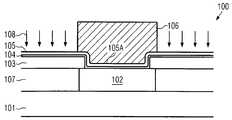
도1a는 제조 단계에서 통상적인 반도체 디바이스(100)의 단면을 도시한 단면도이다. 반도체 디바이스(100)는 기판(101)을 포함하며, 상기 기판(101)에는 회로 소자들 및 다른 미세구조 피쳐들이 형성되어 있는바, 편의를 위해서 이들은 도1a에 도시되어 있지 않다. 또한, 디바이스(100)는 구리 기반의 금속 배선과 비아들을 포함하는 하나 이상의 금속화층을 포함하여 구성되는바, 편의를 위해서 최종 금속화층(107)이 도시되어 있다. 상기 금속화층은 유전 물질을 포함할 수 있으며 그리고 실질적으로 구리 또는 구리 합금을 포함하는 금속 영역(102)이 그 안에 형성되어 있다. 금속 영역(102)의 적어도 소정 부분을 제외하고, 상기 금속화층(107)은 페시베이션층(103)으로 커버된다. 페시베이션층(103)은 임의의 적절한 유전물질들, 예컨대 실리콘 이산화물, 실리콘 질화물, 실리콘 산화질화물 등등을 포함할 수 있다. 구리 기반의 상기 금속 영역(102) 위에는, 탄탈륨, 탄탈륨 질화물, 티타늄, 티타늄 질화물, 탄탈륨 질화물 또는 이들의 화합물 등등을 포함하여 구성된 장벽/접착 층(104)이 형성되며, 상기 장벽/접착 층(104)은, 위에 놓은 알루미늄층(105)과 구리 기반의 금속 영역(102) 사이에서 접착을 제공할 뿐만 아니라, 요구되는 확산 차단 특성을 제공한다. 상기 알루미늄층(105)은 장벽/접착 층(104)과 더불어 단자 금속이라고 지칭될 수도 있다. 따라서, 상기 알루미늄층(105)은, 페시베이션층(103), 장벽/접착 층(104) 및 아래에 놓인 구리 기반의 금속 영역(102)과 함께 콘택 영역(105A)을 정의하며, 상기 콘택 영역(105A) 위에는 솔더 범프가 형성될 것이다. 또한, 알루미늄을 효과적으로 제거하기 위해서 염소(chlorine) 기반의 화학제를 전형적으로 포함하고 있는 식각 앰비언트(etch embient)(108)에 상기 층(105)의 나머지 부분을 노출시키는 동안에 콘택 영역(105A)을 보호하기 위해서, 상기 디바이스 상에는 대응 레지스트 마스크(106)가 형성된다.1A is a cross-sectional view showing a cross section of a
도1a에 도시된 바와 같은 반도체 디바이스(100)는 다음의 공정들에 의해 형성될 수 있다. 먼저, 잘 정립된 공정 기법에 기초하여 기판(101) 및 기판에 포함된 임의의 회로 소자들이 형성될 수 있다. 정교한 응용예들의 경우에는, 약 50nm 이하의 작은 임계치수를 갖는 회로소자들이 형성될 수도 있으며, 이어서 구리 기반의 금속배선들과 비아들을 포함하는 하나 이상의 금속화층들(107)이 형성되는바, 통상적으로 로우-k 유전물질이 적어도 하나의 금속 배선을 수납하기 위해서 이용될 수 있다. 다음으로, 플라즈마 증강 화학 기상 증착법(PECVD) 등등과 같은 임의의 적절한 증착법에 의해서 페시베이션층(103)이 최종 금속화층(107) 상에 형성된다. 다음으로, 표준 포토리소그래피 공정이 수행되어, 콘택 영역(105A)의 형태와 치수를 실질적으로 결정하는 소정 형태와 치수를 갖는 포토레지스트 마스크(미도시)가 형성되는바 이는, 상기 층들(104, 105)의 물질 특성들과 조합하여, 금속화층(107)(즉, 구리 기반의 금속 영역 102)과 상기 콘택 영역(105A) 상에 형성될 예정인 솔더 범프 사이에서 최종적으로 얻어진 전기적인 접속의 콘택 저항을 실질적으로 결정한다. 다음으로, 레지스트 마스크에 기초하여 상기 페시베이션층(103)이 오픈될 수 있다. 상기 레지스트 마스크는, 필요에 따라 적절한 세정 단계를 포함할 수도 있는 잘 정립된 레지스트 제거 공정에 의해서 후속으로 제거될 수 있다.The
다음으로, 예컨대, 스퍼터 증착법에 의해서 장벽/접착 층(104)이 형성될 수 있는바, 탄탈륨, 탄탈륨 질화물, 티타늄, 티타늄 질화물 또는 다른 유사한 물질 및 이들의 화합물에 대해 잘 정립된 공정 레시피를 이용하여 형성될 수 있다. 상기 물질들은 구리 확산을 효과적으로 방지하며 그리고 위에 놓인 알루미늄층(105)과의 접착을 강화하기 위해서 전형적으로 이용되는 것들이다. 다음으로, 가령 스퍼터 증착, 화학 기상 증착 등등에 의해서 알루미늄층(105)이 형성될 수 있으며, 이어서 레지스트 마스크(106)를 형성하기 위한 표준 포토리소그래피 공정이 수행된다. 다음으로, 반응성 식각 앰비언트(108)가 설정될 수도 있는바, 이는 염소(chlorine) 기반의 복잡한 식각 화학제를 필요로 할 수도 있다. 여기서, 공정 파라미터들은 부당한 수율 감소를 방지하기 위해서 정교한 공정 제어를 필요로 할 수 있다. 또한, 상기 식각 공정(108)은 장벽/접착 층(104)을 관통하는 별도의 식각 단계를 포함할 수도 있으며, 그리고 복잡한 알루미늄 식각 단계 동안에 생성된 임의의 부식성 식각 잔류물을 제거하기 위한 습식 스트립 공정을 포함할 수도 있다.Next, the barrier /
도1b는 더 진행된 제조 단계에서 반도체 디바이스(100)를 도시한 도면으로, 또 다른 페시베이션층(109)(최종 페시베이션 물질 또는 최종 페시베이션층이라고도 지칭됨)이, 콘택 영역(105A)과 페시베이션층(103) 위에 형성된다. 이어서, 상기 최종 페시베이션층(109)을 오픈시키기 위한 후속 식각 공정에서 식각 마스크로서 기능하는 레지스트 마스크(110)가 형성된다. 상기 최종 페시베이션층(109)은 잘 정립 된 스핀-온 기법 또는 또 다른 증착 방법에 기초하여 형성될 수 있으며, 레지스트 마스크(110)는 포토리소그래피 기법에 기초하여 형성될 수 있다. 상기 레지스트 마스크(110)에 기초하여, 최종 페시베이션층(109)(통상적으로 폴리이미드를 포함하여 구성됨)이 식각되어, 콘택 영역(105A)의 적어도 일부가 노출된다.FIG. 1B illustrates the
또 다른 방법에 따르면, 페시베이션층(103)이 형성되기 이전에, 알루미늄층(105)과 장벽/접착 층(104)이 금속화층(107) 상에 형성될 수도 있다. 다음으로, 페시베이션층(103)이 패터닝될 수 있으며, 이어서 매우 복잡한 알루미늄 식각공정(108)이 수행된다. 상기 알루미늄 식각공정은, 장벽/접착 층(104)도 패터닝하는 임의의 식각공정 및 세정공정을 포함할 수도 있다. 이어서, 최종 페시베이션층(109)이 형성되며, 도1b를 참조하여 앞서 설명된 후속 공정이 계속 진행될 수 있다.According to another method, before the
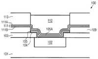
도1c는 더 진행된 제조 단계에서 반도체 디바이스()를 도시한 도면이다. 여기서, 상기 디바이스(100)는 언더범프 금속화층(111)을 포함하며, 이러한 일례에서 언더범프 금속화층(111)은 적어도 제 1 언더범프 금속화층(111A)과 제 2 언더범프 금속화층(111B)을 포함하는 것으로 도시되어 있다. 이들 제 1 및 제 2 언더범프 금속화층(111A, 111B)은 패터닝된 최종 페시베이션층(109)과 콘택 영역(105A) 상에 형성된다. 위에 있는 솔더 범프 물질(112)이 아래에 있는 디바이스 영역 안으로 확산하는 것을 감소(또는 방지)시킬 뿐만 아니라, 요구되는 전기적 특성, 열 관련 특성, 및 기계적 특성들을 제공하기 위해서, 상기 언더범프 금속화층(111)은 적절한 층들의 조합을 포함할 수도 있다. 또한, 레지스트 마스크(113)가 형성되는바, 이는 솔더 범프(112)의 형태 및 측면 치수를 실질적으로 정의하는 개구부를 포함한다.FIG. 1C is a view showing the semiconductor device 에서 in a further manufacturing step. Here, the
일반적으로, 도1c에 도시된 디바이스(100)는 다음의 공정들에 의해 형성될 수 있다. 먼저, 언더범프 금속화층(111), 예컨대 상기 층(111B)이, 티타늄 텅스텐층(TiW)을 형성하기 위한 스퍼터 증착법에 의해서 형성될 수 있는바, 이러한 물질 조성은 충분히 입증된 확산 차단 특성 및 접착 특성을 보여주므로 자주 이용되고 있다. 다음으로, 상기 층(111A)과 같은 언더범프 금속화층(111)의 또 다른 서브-층(sub-layer)이 형성될 수 있는바, 이는 크롬/구리 층의 형태로 제공될 수 있으며, 이어서 실질적으로 순수한 구리층이 추가로 형성될 수도 있다. 상기 층(들)(111A)은, 잘 정립된 레시피에 따라 스퍼터 증착으로 형성될 수 있다. 다음으로, 레지스트 마스크(113)를 형성하기 위한 후속 포토리소그래피 공정이 수행되는바, 이에 의해 솔더 범프(112)를 형성하기 위한 후속 전기도금 공정의 증착 마스크가 제공될 수 있다. 다음으로, 레지스트 마스크(113)가 제거되며, 그리고 솔더 범프(112)를 식각 마스크로 이용하여 상기 언더범프 금속화층(111)이 패터닝될 수 있는데, 이에 의해 전기적으로 절연된 솔더 범프들(112)이 얻어진다. 공정 요구사항에 따라, 원형(rounded) 솔더 볼(미도시)을 생성하기 위해서 솔더 범프(112)가 리플로우될 수도 있으며, 이후 솔더 볼은, 적절한 캐리어 기판과의 접촉을 위해 이용될 수 있다.In general, the
도1a 내지 도1c를 참조하여 설명된 공정 플로우에서 알 수 있는 바와 같이, 콘택 영역(105A)을 제공하여, 솔더 범프(112)와 그 아래에 놓인 언더범프 금속화층(111)을 포함하는 범프 구조를 형성하기 위해서는, 매우 복잡한 공정 플로우를 필요로 한다. 더 나아가, 비록 금속 영역(102)에 대해서 높은 전도도의 구리가 이용되고 있긴 하지만, 최종적으로 얻어진 범프 구조의 콘택 저항은, 콘택 영역(105A)의 특성, 즉 상기 알루미늄층(105)과 장벽/접착 층(104)에 의해 상당한 영향을 받는다. 결과적으로, 통상적인 공정에서는, 복잡한 알루미늄 식각공정을 포함하는 매우 복잡한 공정 플로우가 이용되고 있지만, 최종 범프 구조에 관해서는 중간 정도의 전기적인 성능을 얻을 수 있을 뿐이다. 또한, 알루미늄 피팅(aluminum pitting)과 일반적으로 폴리이미드를 포함하여 구성된 최종 페시베이션층(109)의 박리(delamination)가 발생할 수도 있는바, 이는 특히 오픈된 구리 영역(즉, 상기 영역(102)과 유사한 영역이며 오픈 영역이라고도 지칭됨)에 의해 야기되며, 상기 영역은 다이 경계로서 기능하기 위해서 다이의 에지 영역에 제공되거나 또는 스크라이브 레인(scribe lane)이 전면(front side)에 제공되는 경우 웨이퍼의 스크라이브 레인에 제공되는 것이 일반적이다. 이러한 오픈 영역에는, 최종 페시베이션층(109)이 제공되지 않을 수도 있으며, 따라서 오픈 영역들과 정규 다이 영역들 사이의 임의의 계면에서 폴리이미드층(109)의 박리를 촉진할 수 있다. 따라서, 알루미늄 피팅 및/또는 폴리이미드 박리는, 전술한 바와 같은 제조 단계들에서 수율 감소에 상당한 기여를 할 수도 있다 .As can be seen in the process flow described with reference to FIGS. 1A-1C, a bump structure comprising a
본 발명은, 전술한 바와 같은 하나 이상의 문제점들의 영향을 회피 또는 적어도 감소시키는 다양한 디바이스들 및 방법들에 관한 것이다.The present invention is directed to various devices and methods that avoid or at least reduce the effects of one or more of the problems described above.
다음에 설명될 내용은 본 발명에 대한 요약으로서, 이는 본 발명의 몇몇 양상에 대한 기본 이해를 제공하기 위한 것이다. 이러한 요약은 본 발명에 대한 완전한 개괄은 아니다. 이러한 요약은 본 발명의 핵심적인 요소 또는 중요한 요소들을 식별하기 위한 것이 아니며, 본 발명의 범위를 제한하고자 의도된 것이 아니다. 이러한 개요의 주된 목적은, 후술될 발명의 상세한 설명에 앞서서, 본 발명의 몇 가지 개념들을 간단한 형식으로 제공하기 위한 것이다.The following is a summary of the invention, which is intended to provide a basic understanding of some aspects of the invention. This summary is not an exhaustive overview of the invention. This summary is not intended to identify key elements or critical elements of the invention, but is not intended to limit the scope of the invention. Its main purpose is to present some concepts of the invention in a simplified form prior to the following description of the invention.
일반적으로, 본 발명은 언더 범프 금속화층과 최종 금속화층의 콘택 영역(가령, 구리 기반의 금속 영역)에 상에 직접 놓여있는 솔더 범프 또는 임의의 다른 접착성 범프 물질을 포함하는 범프 구조의 형성을 가능케하는 기법에 관한 것으로, 이에 의하면 매우 복잡한 장벽/접착 층 공정, 알루미늄 증착공정 및 패터닝 공정을 회피할 수 있다. 따라서, 종래기술에 따른 공정과 비교하면, 제조 시퀀스가 좀더 효율적으로 설계될 수 있으며, 그러므로 제조 비용을 감소시킬 수 있는바, 이와 동시에 범프 구조의 전기적, 기계적, 열관련 특성들 범프 구조의 성능을 향상시킬 수 있다.In general, the present invention contemplates the formation of a bump structure comprising a solder bump or any other adhesive bump material directly lying on the under bump metallization layer and a contact region (eg, a copper based metal region) of the final metallization layer. It is possible to avoid very complex barrier / adhesive layer processes, aluminum deposition processes and patterning processes. Therefore, compared with the process according to the prior art, the manufacturing sequence can be designed more efficiently, and therefore, the manufacturing cost can be reduced, while at the same time the electrical, mechanical and thermal properties of the bump structure can be improved. Can be improved.
본 발명의 예시적인 일실시예에 따르면, 반도체 디바이스는 금속화층을 포함하는바, 상기 금속화층은 페시베이션층에 의해 측면적으로 접경하며 그리고 콘택 표면을 갖는 콘택 영역을 포함한다. 또한, 상기 디바이스는 페시베이션층 위에 형성된 최종 페시베이션층을 포함하며 그리고 상기 콘택 영역의 적어도 일부를 노출시킨다. 언더범프 금속화층이 콘택 영역 및 최종 페시베이션층의 일부 상에 형성되며, 그리고 니켈-함유 중간층이 언더범프 금속화층 상에 형성된다. 마지막으로, 니켈-함유 중간층 상에 범프가 형성된다.In accordance with one exemplary embodiment of the present invention, a semiconductor device comprises a metallization layer, the metallization layer comprising a contact region bordering laterally by a passivation layer and having a contact surface. The device also includes a final passivation layer formed over the passivation layer and exposes at least a portion of the contact region. An under bump metallization layer is formed on the contact region and a portion of the final passivation layer, and a nickel-containing intermediate layer is formed on the under bump metallization layer. Finally, bumps are formed on the nickel-containing intermediate layer.
본 발명의 다른 실시예에 따르면, 소정 방법이 제공되는바, 상기 방법은 반도체 디바이스의 최종 금속화층의 콘택 영역의 노출된 콘택 표면 상에 언더범프 금속화층을 형성하는 단계를 포함한다. 또한, 상기 방법은 니켈-함유 중간층을 상기 언더범프 금속화층 상에 형성하는 단계와 상기 콘택 표면 위의 상기 니켈-함유 중간층 상에 범프를 형성하는 단계를 포함한다. 추가적으로는, 범프의 존재하에서 상기 언더범프 금속화층이 패터닝된다.According to another embodiment of the present invention, a method is provided, which includes forming an under bump metallization layer on an exposed contact surface of a contact region of a final metallization layer of a semiconductor device. The method also includes forming a nickel-containing intermediate layer on the under bump metallization layer and forming a bump on the nickel-containing intermediate layer over the contact surface. Additionally, the under bump metallization layer is patterned in the presence of bumps.
본 발명의 또 다른 실시예에 따르면, 소정 방법이 제공되는바, 상기 방법은 반도체 디바이스의 최종 금속화층 위에 니켈-함유층을 형성하는 단계를 포함하며, 여기서 상기 니켈-함유층은 습식 화학 공정에 의해서 형성된다. 또한, 범프 구조가 상기 니켈-함유층 위에 형성된다.According to yet another embodiment of the present invention, a method is provided, the method comprising forming a nickel-containing layer over a final metallization layer of a semiconductor device, wherein the nickel-containing layer is formed by a wet chemical process. do. In addition, a bump structure is formed on the nickel-containing layer.
본 발명은 첨부된 도면들을 참고하고 다음에 후술될 발명의 상세한 설명을 참조하여 이해될 것인바, 도면들에서 유사한 구성요소들은 유사한 참조번호들을 갖는다.BRIEF DESCRIPTION OF THE DRAWINGS The present invention will be understood with reference to the accompanying drawings and with reference to the following detailed description of the invention, in which like elements have similar reference numerals.
도1a 내지 도1c는 최종 금속화층의 구리 기반의 금속 영역 위에 범프 구조를 형성하는 동안에 통상적인 반도체 디바이스의 단면을 도시한 단면도이다.1A-1C are cross-sectional views showing cross-sections of conventional semiconductor devices during the formation of bump structures on copper-based metal regions of the final metallization layer.
도2a 내지 도2d는 본 발명의 예시적인 실시예에 따라 구리-함유 표면 상에 범프 구조를 직접 형성하는 동안에 반도체 디바이스의 단면을 도시한 단면도이다.2A-2D are cross-sectional views of cross-sections of semiconductor devices during the direct formation of bump structures on copper-containing surfaces in accordance with exemplary embodiments of the present invention.
비록, 본 명세서에 개시된 본 발명의 내용은 다양한 수정예들 및 대안 형태들이 가능하나, 이에 대한 특정한 실시예들이 상기 도면들에 일례로서 예시되어 있 으며, 이하에서 상세히 설명된다. 그러나, 특정 실시예들에 대한 하기의 설명은, 본 발명을 개시된 특정한 형태에 한정시키고자 의도된 것이 아니며, 이와 반대로 첨부된 특허청구범의에 정의된 바와 같이 본 발명의 사상 및 범위 내에서 모든 수정예들, 동등물 및 대안적 형태들을 모두 커버하도록 의도되었다는 점을 유의해야 한다.Although the subject matter disclosed herein is capable of various modifications and alternative forms, specific embodiments thereof are illustrated by way of example in the drawings and are described in detail below. However, the following description of specific embodiments is not intended to limit the invention to the particular forms disclosed, and conversely, all modifications within the spirit and scope of the invention as defined in the appended claims. It should be noted that it is intended to cover all examples, equivalents, and alternative forms.
본 발명의 다양한 예시적인 실시예들이 아래에 설명된다. 명료함을 위하여, 실제 구현예의 모든 특징들이 본 명세서에 기술되는 것은 아니다. 이러한 임의의 실제 구현예를 개발하는데 있어서, 개발자들의 특정한 목적(가령, 시스템과 관련된 제한사항 그리고 사업상의 제한 사항에 부합시키는 것)을 달성하기 위해, 구현예별로 특정한 많은 사항들이 결정되어야만 한다는 점이 이해되어야 한다. 더 나아가, 이러한 개발 노력은 복잡하고 시간이 걸리는 일일수 있지만, 그럼에도 불구하고 본 명세서에 개시된 내용에 의해 도움을 받는 당업자에게는 이러한 개발 노력이 통상적인 작업일 수도 있음이 이해되어야만 한다.Various exemplary embodiments of the invention are described below. In the interest of clarity, not all features of an actual implementation are described in this specification. In developing any of these practical implementations, it is understood that many implementation specific issues must be determined in order to achieve the specific objectives of the developer (e.g. meeting system and business limitations). Should be. Furthermore, such development efforts may be complex and time consuming, but it should nevertheless be understood that such development efforts may be routine to those skilled in the art to be assisted by the disclosure herein.
이하, 첨부된 도면을 참조하여 본 발명이 설명될 것이다. 다양한 구조, 시스템 및 장치들이 설명만을 위한 목적으로 도시되었으며, 그리고 당업자들에게 잘 알려진 상세한 내용으로 본 발명의 의미를 모호하게 만들지는 않기 위하여 상기 도면들에 개략적으로 묘사되어 있다. 그럼에도 불구하고, 상기 첨부된 도면들은 본 발명의 실시예들을 서술 및 설명하기 위해 포함된 것들이다. 본 명세서에서 이용되는 용어 및 구절들은, 관련기술의 당업자들에 의해 상기 용어 및 구절들이 이해되는 바와 일관된 의미를 갖도록 이해 및 해석되어야 한다. 용어 혹은 구절에 대한 특별한 정의 즉, 당업자들이 이해하는 바와 같은 일반적이고 통상적인 의미와는 다른 정의는, 본 명세서에서 상기 용어 혹은 구절을 일관적으로 사용하는 것에 내포되지는 않을 것이다. 용어 혹은 구절이, 특별한 의미, 즉, 당업자들에 의해 이해되는 바와는 상이한 의미를 갖는 경우, 이러한 특별한 정의는 용어 혹은 구절에 대한 특별한 정의를 직접 및 간접적으로 제공하는 방식으로 본 명세서에서 설명될 것이다.Hereinafter, the present invention will be described with reference to the accompanying drawings. Various structures, systems and devices have been shown for purposes of illustration only, and are schematically depicted in the drawings in order not to obscure the meaning of the invention in details that are well known to those skilled in the art. Nevertheless, the attached drawings are included to describe and explain embodiments of the present invention. Terms and phrases used herein should be understood and interpreted to have a meaning consistent with those terms and phrases understood by those skilled in the relevant art. Specific definitions of terms or phrases, that is, definitions other than the general and common meanings as those skilled in the art will understand, will not be implied herein in the consistent use of the terms or phrases. Where terms or phrases have special meanings, that is, different meanings as understood by those of ordinary skill in the art, such particular definitions will be described herein in a manner that directly and indirectly provides particular definitions of terms or phrases. .
일반적으로, 본 명세서에 개시된 본 발명의 기술적 사상은 범프 구조를 형성하기 위한 개선된 기법에 관한 것이다. 본 발명에 따르면, 최종 금속화층을 형성하기 위한 공정 플로우와 최종 페시베이션층을 포함하는 범프 구조를 형성하기 위한 공정 플로우 및 물질들을 적절히 조절함으로써, 가령, 구리 함유 영역과 같은 금속 영역의 최상부에 알루미늄층과 같은 단자 금속층을 형성하는 것을 생략할 수 있는바, 따라서 가령, 구리 기반의 금속화와 같은 진보된 금속화 공정(advanced metallization)의 성능과 범프 구조를 형성하기 위한 대응 제조 시퀀스가 개선될 수 있다. 예를 들어, 단자 알루미늄층의 증착을 회피함으로써, 전체 공정 플로우의 복잡도가 상당한 정도로 감소될 수 있으며, 제조 비용을 절감할 수 있는바, 이와 동시에 범프 구조의 전기적 특성 및/또는 기계적 특성 및/또는 열관련 특성들이 개선될 수 있으며, 또는 범프 구조의 주어진 성능에 대해서, 통상적인 반도체 디바이스와 비교하여 범프 구조의 치수가 상당한 정도로 감소될 수 있다. 예를 들어, 종래 디바이스와 동일한 치수의 범프 구조를 갖는 반도체 디바이스는, 상당히 개선된 전류 구동 능력을 가질 수 있으며 또한, 향상된 열 소산(dissipation) 능력을 제공 할 수도 있는데, 이는 부가적이면서도 전도도가 낮은 단자 금속층을 생략함으로써 얻게되는 결과적인 범프 구조의 개선된 열 전도도 및 전기 전도도 때문이다.In general, the technical idea of the invention disclosed herein relates to an improved technique for forming a bump structure. According to the present invention, by appropriately adjusting the process flow and materials for forming the bump structure including the final passivation layer and the process flow for forming the final metallization layer, for example, aluminum on top of a metal region such as a copper containing region Forming a terminal metal layer, such as a layer, can be omitted, so that the performance of advanced metallization, such as copper based metallization, and the corresponding fabrication sequences for forming bump structures, for example, can be improved. have. For example, by avoiding the deposition of the terminal aluminum layer, the complexity of the overall process flow can be reduced to a significant extent and the manufacturing cost can be reduced, while at the same time the electrical and / or mechanical and / or mechanical properties of the bump structure Heat related properties can be improved, or for a given performance of the bump structure, the dimensions of the bump structure can be reduced to a significant extent compared to conventional semiconductor devices. For example, a semiconductor device having a bump structure of the same dimensions as a conventional device may have a significantly improved current driving capability and may also provide an improved heat dissipation capability, which is additional and low in conductivity. This is because of the improved thermal and electrical conductivity of the resulting bump structure obtained by omitting the terminal metal layer.
도2a는 진행된 제조 단계에서 반도체 디바이스(200)의 단면을 도시한 단면도이다. 디바이스(200)는 기판(201)을 포함하는바, 상기 기판은 가령, 벌크 실리콘 기판, 실리콘-온-절연체(Silicon-On-Insulator : SOI) 기판, 회로 소자를 형성하기 위해 임의의 적절한 반도체층 상에 형성된 글래스 기판, 또는 Ⅱ-Ⅵ 및/또는 Ⅲ-Ⅴ 반도체들과 같은 반도체 물질의 임의의 다른 화합물 등등과 같은, 집적회로를 형성하기 위한 임의의 적절한 기판을 나타낸다. 따라서, 기계 소자, 광학 소자 등등과 같은 다른 미세구조 피쳐들과 조합될 수도 있는 다수의 회로 소자들(미도시)이 상기 기판(201) 안에 및 상에 형성된다. 상기 기판(201) 위에는 하나 이상의 금속화층(207)이 형성되는데, 편의를 위해서 상기 금속화층(207)은 최종층을 나타낼 수도 있으며, 이는 실리콘 이산화물, 실리콘 질화물, 불소(fluorine) 도핑된 실리콘 산화물, 3.0 이하의 비유전율(relative permittivity)을 갖는 임의의 로우-k 유전물질 또는 이들의 조합과 같은, 적절한 유전 물질을 포함한다. 또한, 금속화층(207)은 콘택 영역(202)을 포함하는바, 상기 콘택 영역(202)은, 진보된 디바이스에서는 구리 기반의 금속 영역, 즉 우수한 열 전도도 및 전기 전도도를 제공하기 위해서 상당한 정도의 구리를 포함하는 금속 영역이 될 수도 있다. 상기 콘택 영역(202)은 다른 금속들 또는 전도성 물질들을 포함할 수도 있다는 점을 유의해야 하는바, 예를 들면 임의의 장벽/접착 층들이 금속화층(207)의 주위 유전물질과의 경계에 형성될 수도 있다. 상기 콘택 영역(202)은 콘택 표면(202A)을 포함하며, 콘택 표 면(202A) 상에는 범프 구조가 직접 형성된다. 따라서, 형성될 예정인 범프 구조와 금속화층(207) 사이에서 개선된 열 전도도 및 전기 전도도를 제공할 수 있다.2A is a cross-sectional view showing a cross section of the
금속화층(207)은 구리 함유 표면(202A)을 제외하고 페시베이션층(203)에 의해 커버될 수 있는바, 여기서 상기 페시베이션층(203)은 가령, 실리콘 이산화물, 실리콘 질화물, 실리콘 카바이드, 질소-풍부(nitrogen-enriched) 실리콘 카바이드, 로우-k 유전물질 또는 이들 물질들의 적절한 조합과 같은, 임의의 적절한 유전물질을 포함할 수 있다. 예를 들어, 상기 페시베이션층(203)은 2개 이상의 서브층들(203A, 203B, 203C)로 구성될 수 있는바, 최하위 서브층(203A)은 확산 방지 효과를 제공하여, 인접한 디바이스 영역 안으로 구리가 확산되는 것을 실질적으로 억제할 수 있다. 또한, 상기 층(203A)은, 층(203)을 패터닝하는 동안에 적절한 식각정지 특성을 나타낼 수도 있다. 예를 들어, 질소-풍부 실리콘 카바이드가 이용될 수 있다. 다른 경우에 있어서, 상기 층(203A)은 생략될 수도 있으며 그리고 또 다른 층들(203B, 203C)이 요망되는 전체 특성을 제공할 수도 있다. 예컨대, 실리콘 질화물과 함께 실리콘 산화질화물이 이용될 수 있으며, 반면에 다른 실시예에서는 실리콘 이산화물과 실리콘 질화물이 결합될 수도 있다. 하지만, 또 다른 경우에 있어서는, 디바이스의 특성에 따라, 페시베이션층(203)의 임의의 다른 조합이 이용될 수도 있다.The
몇몇 예시적인 실시예들에서, 상기 표면(202A)은 보호층(미도시)에 의해 커버될 수도 있는바, 예시적인 일실시예에서 이는 가령, 층(203A)과 같은 상기 페시베이션층(203)의 일부를 나타낼 수도 있다. 다른 예시적인 실시예에서는, 별도의 층으로서 보호층이 페시베이션층(203)과 표면(202A) 상에 형성될 수도 있다. 각 보호층은 가령, 실리콘 질화물, 실리콘 카바이드, 질소-풍부 실리콘 카바이드 등등과 같은 임의의 적절한 유전물질을 포함할 수 있으며, 그리고 반도체 디바이스(200)의 후속 공정 및 처리 동안에 상기 표면(202A)을 실질적으로 보호할 수 있다.In some exemplary embodiments, the
또한, 도시된 실시예에서, 상기 디바이스(200)는 최종 페시베이션 물질(209)을 포함하며, 이는 예시적인 실시예들에서 폴리이미드(polyimide) 등등을 포함하여 구성된다. 다른 실시예에서, 상기 최종 페시베이션 물질(209)은, 광 민감(photosensitive) 폴리이미드와 같은 광 민감 물질을 포함할 수 있다. 또한, 상기 층(203) 내에, 상기 층(203)의 적어도 상위 부분에 개구부(215)가 형성될 수 있으며 이 경우, 표면(202A)은 층(203)의 소정부분에 의해 여전히 커버될 수 있다. 그리고 상기 층(209)에 개구부가 형성된다. 개구부(215)의 수평 사이즈는, 최종 콘택 영역은 상기 표면(202A)을 노출시키고 그리고 각각의 범프 구조를 그 위에 형성한 다음 최종 금속화층(207)과 접촉하는 최종 콘택 영역의 사이즈를 실질적으로 정의한다.In addition, in the illustrated embodiment, the
도2a에 도시된 반도체 디바이스(200)를 형성하는 전형적인 공정 플로우는 다음의 공정들을 포함할 수 있다. 소정의 공정 레시피와 설계 규칙에 따라, 임의의 회로 소자들 및 가능하다면 다른 미세구조 피쳐들을 기판(201)에 형성한 다음에, 구리 기반의 금속 배선들 비아들을 형성하기 위한 잘 정립된 다마신(damascene) 기법에 기초하여 하나 이상의 금속화층(207)들이 형성될 수 있다. 금속화층들(207)을 형성하는 동안에, 표면(202A)을 갖는 콘택 영역(202)이 또한 형성될 수도 있다. 다 음으로, 상기 금속화층(207)을 신뢰성 있게 커버하기 위하여, 가령 PECVD 법과 같은 적절한 증착 기법에 의해 페시베이션층(203)이 형성된다. 전술한 바와 같이, 페시베이션층(203)은, 인접한 디바이스 영역으로 구리 원자가 확산되는 것을 실질적으로 억제하는 소정 물질을 포함할 수 있다. 이후, 예시적인 일실시예에서는, 예컨대 스핀-온 기법 등등에 기초하여 최종 페시베이션층이 형성될 수도 있다. 예를 들어, 상기 물질(209)은 광 민감 물질로서 적용될 수도 있는바, 이는 물질(209)을 선택적으로 노출시킬 수 있는 리소그래피 공정에 기초하여 패터닝될 수 있다. 다음으로, 이전의 노출 공정에 의해서 상기 물질(209)에 형성된 잠상(latent image)에 기초하여 상기 물질(209)이 패터닝된다. 다음으로, 상기 패터닝된 물질(209)은, 잘 정립된 식각 기법에 의해서 페시베이션층(203)을 식각하기 위한 식각 마스크로서 이용된다. 전술한 바와 같이, 몇몇 실시예에서, 기판(2041)을 후속 처리하는데 있어서 보호층이 있는 것이 바람직한 경우에는, 상기 표면(202A)이 완전히 노출되기 전에 상기 층(203)에 대한 패터닝이 중단될 수도 있다. 예를 들어, 식각 정지층으로서 기능할 수도 있는 상기 층(203A)은, 표면(202A) 상에 후속 물질을 형성하는 공정이 수행되기 바로 직전에 오픈될 수도 있다. 하지만, 상기 물질(209) 및 상기 층(203)을 패터닝하기 위해서, 또 다른 공정 플로우가 이용될 수도 있다. 예를 들어, 레지스트 마스크가 상기 물질(209) 위에 형성될 수 있으며, 그리고 레지스트 마스크에 기초하여 상기 물질(209) 및 상기 층(203)이 패터닝될 수 있는바, 이는 몇몇 실시예에서, 통상적인 식각 공정에 의해 수행될 수 있다. 반면에, 다른 경우들에 있어서, 상기 레지스트 마스크는 상기 물질(209)을 식각한 다음에 제거될 수 있다. 이후, 상기 물질(209)이 상기 층(203)에 대한 식각 마스크로서 기능할 수 있다. 전술한 바와 같이, 우수한 열 전도도 및 전기 전도도를 갖는 범프 구조가 형성될 것이기 때문에, 상기 개구부(215)의 치수는 유사한 열 전도도 및 전기 전도도를 갖는 통상적인 디바이스 보다 작게 선택될 수 있다. 결과적으로, 솔더 범프 등등을 형성하는 후속 프로세스에서 상당한 양의 물질을 절감할 수 있다. 다른 한편으로, 기결정된 치수를 갖는 개구부(215)에 대해서, 최종적으로 얻어진 열 전도도 및 전기 전도도는 종래의 디바이스에 비하여 상당히 개선될 수 있다.A typical process flow for forming the
도2b는 더 진행된 제조 단계에서 반도체 디바이스(200)를 도시한 것으로, 여기서 상기 표면(202A)은 가령, 층(203A)과 같은 보호층에 의해서 신뢰성 있게 커버될 수도 있다. 반면에 다른 실시예에서 상기 표면(202A)은 노출될 수 있으며 그리고 언더범프 금속화층의 후속 증착 이전에 세정 처리를 필요로 할 수도 있다. 따라서, 도시된 상기 디바이스(200)는 표면(202A)을 노출 및/또는 세정하기 위한, 적절하게 설계된 표면 처리 공정(217)을 받게될 것이다. 예시적인 일실시예에서, 상기 표면 처리 공정(217)은, 노출된 구리 표면 상에 임의의 적절한 금속을 스퍼터 증착하기 전에 전형적으로 이용되는 것과 같은 선-세정 공정(pre-cleaning process)으로 설계된다. 따라서, 상기 공정(217)은, 아르곤 등등과 같은 비활성 종들(inert species)의 충분한 폭격(bombardment)을 제공하기 위해 적절히 선택된 파라미터들을 갖는 선-스퍼터 공정(pre-sputter process)으로서 설계될 수 있는바, 이는 예컨대, 실리콘 질화물, 질소-함유 실리콘 카바이드 등등을 포함할 수 있는 원하지 않는 물질을 제거하기 위한 것이다. 결과적으로, 공정(217) 동안에, 상기 표면(202A) 은 점진적으로 노출될 수 있으며 반면에, 진행중인 상기 이온 폭격은 바람직하지 않은 변색(discoloration)과 산화 부분이 상기 표면(202A) 상에 형성되는 것을 실질적으로 억제한다. 일실시예에서, 표면(202A)으로부터 물질을 제거하기 위한 상기 공정(217)의 공정 파라미터(예컨대, 전구체 물질의 공급)는, 최종 페시베이션층(209)의 노출된 부분들과 노출된 상기 표면(202A) 상에 전도성 언더범프 금속화층을 형성하기 위한 스퍼터 증착 환경(atmosphere)을 후속으로 설정하기 위해서 인 시츄(in situ)로 변형될 수도 있다. 또 다른 패터닝 기법이 이용될 수 있다는 점을 유의해야 하는바, 페시베이션층(203)에 형성된 각각의 개구부와는 상이한 사이즈의 개구부를 갖도록 상기 최종 페시베이션층(209)이 패터닝될 수도 있다. 이러한 경우, 2개의 상이한 패터닝 공정이 이용될 수 있는바, 여기서 상기 세정 처리(217)는 층들(209, 203)의 다양한 노출 부분들 상에 적용될 수도 있으며, 반면에 후속 증착 공정은, 상기 층(203)의 노출된 수평 부분들 상에도 물질을 형성할 수 있다.FIG. 2B illustrates the
도2c는 스퍼터 증착공정(219)에 의해서 언더범프 금속화층(211)을 또는, 적어도 서브층(211B)을 형성하는 동안에 반도체 디바이스(200)를 도시한 도면이다. 예시적인 일실시예에서, 상기 스퍼터 증착공정(219)은, 가령, 티타늄 텅스텐, 탄탈륨, 티타늄, 질화티타늄, 질화탄탈륨, 텅스텐, 텅스텐 실리사이드, 티타늄 실리사이드, 탄탈륨 실리사이드, 또는 질소-풍부 텅스텐, 탄탈륨 및 티타늄 실리사이드 등등과 같은 임의의 적절한 금속 또는 금속 화합물을 형성하도록 설계될 수 있다. 이들 실시예에서, 선행 세정공정으로서 상기 공정(217)(도2b)이 인 시츄(in situ)로 수행될 수도 있는바, 여기서는 바람직하지 않은 물질들을 표면(202A)으로부터 제거한 이후에, 아르곤 이온, 금속 이온, 및 질소와 실리콘과 같은 다른 전구체 물질의 비율이 변경될 수도 있는데, 이는 상기 층(211B)을 효과적으로 증착하기 위함이다. 결과적으로, 종래기술에서 사용되었던 임의의 중간 단자 금속을 필요로 함이 없이, 노출된 표면(202A) 상에 언더범프 금속화층(211), 즉 제 1 서브층(211B)이 직접 형성된다. 예시적인 실시예에서, 상기 서브층(211B)은 티타늄층의 형태로 제공되는바, 따라서 원하는 접착 특성 및 장벽 특성을 제공할 수 있다. 서브층(211B)을 형성한 다음에, 임의의 적절한 물질 조성을 갖는 하나 이상의 추가 서브층들이 예를 들면, 스퍼터 증착, 전기화학 증착, 화학기상증착(CVD) 등등에 의해서 증착될 수 있는바, 이는 디바이스의 요구사항들에 따라 언더범프 금속화층(211)의 형성을 완료하기 위한 것이다. 예를 들어, 일 실시예에서는, 니켈-함유 물질을 증착하기 위한 후속 습식 화학 증착공정에서의 시드층(seed layer)으로서 기능하기 위해서, 구리 함유층이 형성될 수도 있다. 따라서, 예시적인 몇몇 실시예들에서 상기 언더범프 금속화층(211)은, 티타늄을 포함하는 제 1 서브층(211B)과 구리 및/또는 후속 습식 화학 증착공정을 개시하기 위한 임의의 적절한 시드 물질을 포함하는 제 2 서브층(211A)을 포함할 수도 있다. 하지만, 임의의 적절한 또 다른 층 순서(layer sequence) 및 물질 조성들이 상기 층(211)에 대해서 적용될 수도 있다는 점을 유의해야 한다.FIG. 2C shows the
도2d는 더 진행된 제조 단계에서 디바이스(200)를 도시한 도면이다. 레지스트 마스크(213)가 제공되는바, 이는 레지스트 마스크(213)의 개구부 내에 형성되는 범프(212)의 측면 치수(lateral dimension)를 정의한다. 또한, 언더범프 금속화 층(211)과 범프(212) 사이에는 중간층(216)이 형성되는데, 예시적인 몇몇 실시예에서 상기 중간층(216)은 니켈 함유층이 될 수도 있다. 본 발명의 일실시예에서, 상기 중간층(216)은 니켈을 포함할 수도 있으며, 반면에 다른 실시예에서는 니켈 화합물이 이용될 수도 있다. 또 다른 실시예에서는 니켈 함유층 및 구리 함유층의 스택이 제공될 수도 있는바, 따라서 범프 구조의 전도도가 증가될 수 있다. 상기 중간층(216) 내의 니켈 물질은 범프를 형성하기 위한 후속 공정 동안에 향상된 성능을 제공할 수도 있으며, 그리고 동작 행동(operational behavior)에 대해서 향상된 성능을 제공할 수도 있다. 또한, 예시적인 몇몇 실시예에서는, 레지스트 마스크(213)의 아래에도 상기 중간층(216)이 형성될 수 있는바, 따라서 범프를 형성하기 위한 후속 습식 화학 증착공정 동안에 언더범프 금속화층의 효율을 더욱 개선시킬 수 있다.2D shows the
범프(212)는 납이 많이 함유된 납과 주석의 화합물과 같은 임의의 적절한 물질 조성을 포함할 수 있으며, 또는 상기 물질은 공융 화합물(eutectic compound)이 될 수도 있다. 또 다른 경우에 있어서는, 주석/은 혼합물(tin/silver mixture) 등등과 같은 실질적으로 납이 없는 화합물(lead-free compound)이 이용될 수도 있다. 다른 실시예에서는 디바이스의 요구사항들에 따른 임의의 적절한 물질 조성이 이용될 수 있다. 개구부(215) 내에 중간층(216)을 제공함으로써, 원하는 조성의 물질을 습식 화학으로 증착함에 있어서 개선된 유연성이 얻어질 수 있는데, 이는 예컨대 니켈 함유층이 전기도금법(electroplating) 또는 무전해도금법(electroless plating)에 의해 효과적으로 증착될 수 있으므로, 실제의 범프 물질에 대해 매우 균일하고 전도성이 우수한 "버퍼" 층을 제공할 수 있기 때문이다. 더 나아가, 니켈은, 납 함유 물질 및 무연(lead-free) 물질과 같은 다수의 범프 물질들에 대해서 매우 우수한 친화성(compatibility)을 제공할 수 있으며, 아울러 매우 높은 전도도를 제공할 수 있다.Bump 212 may include any suitable material composition, such as a compound containing lead-containing lead and tin, or the material may be an eutectic compound. In other cases, substantially lead-free compounds may be used, such as tin / silver mixtures and the like. In other embodiments, any suitable material composition may be used depending on the requirements of the device. By providing the
상기 층 또는 층들(211)은 임의의 적절한 증착 기법에 의해서 형성될 수 있으며, 이어서 잘 정립된 포토리소그래피 공정이 수행되어 레지스트 마스크(213)를 형성 및 패터닝한다. 다음으로, 몇몇 실시예서는 전기도금 공정 및/또는 무전해도금 공정에 의해서 중간층(216)이 형성될 수도 있는바, 여기서 상기 언더범프 금속화층(211), 즉 상기 층(211A)은 시드층 또는 촉매 물질(catalyst material)로서 기능할 수도 있다. 따라서, 범프 물질을 한정하기 위한, 신뢰성 있고 그리고 실질적으로 균일한 바닥층이 제공될 수 있다. 다른 실시예에서, 언더범프 금속화층(211)의 향상된 전류 분포 효과가 바람직한 경우에는, 레지스트 마스크(213)를 형성하기 전에 상기 중간층(216)이 형성될 수도 있다.The layer or layers 211 may be formed by any suitable deposition technique, and then a well-established photolithography process is performed to form and pattern the resist
다음으로, 언더범프 금속화층(211)을 전류 분배층으로 이용하여 전기도금법에 의해서 범프(212)가 형성될 수 있으며, 상기 레지스트 마스크(213)는 범프(212)의 측면 치수를 정의한다. 따라서, 상기 디바이스(200)는 범프(212)와 언더범프 금속화층(211)을 포함하는범프 구조를 포함하여 이루어지며, 여기서 상기 언더범프 금속화층(211)은 콘택 영역(202) 상에 즉, 표면(202A) 상에 직접 형성되며, 그리고 범프(212)와 언더범프 금속화층(211) 사이에서 버퍼로서 기능하는 중간층(216)이 구비된다. 또한, 전술한 바와 같이, 단자층(terminal layer)을 제공하지 않아도 되 기 때문에, 콘택 영역(202)과 범프(212) 사이의 열 전도도 및 전기 전도도가 상당히 개선될 수 있으며, 아울러 공정 시간 역시도 감소될 수 있다.Next, a bump 212 may be formed by an electroplating method using the under
다음으로, 잘 정립된 레지스트 제거 기법에 기초하여 레지스트 마스크(213)를 제거함으로써, 후속 공정이 진행될 수 있으며, 이후에는 범프(212)의 존재하에서 언더범프 금속화층(211)이 패터닝되어, 전기적으로 절연된 범프들(212)이 형성된다. 언더범프 금속화층(211)에 대한 패터닝 공정은, 습식화학 식각 및/또는 전기화학 식각 및/또는 플라즈마 기반 식각 기법들을 포함할 수도 있다. 다음으로, 몇몇 실시예들에서, 상기 범프(212)는 솔더 물질을 적절히 리플로우(reflow) 시킴으로써, 솔더 볼로 형성될 수 있다. 다른 일례들에서, 상기 범프(212)는 이전의 리플로우 공정 없이, 적절한 캐리어 기판에 접촉하는데 이용될 수도 있다.Subsequently, by removing the resist
결과적으로, 본 명세서에 개시된 본 발명은, 가령, 구리 기반의 콘택 영역과 같은 콘택 영역 상에 직접 형성된 언더범프 금속화층과 범프를 포함하여 구성된 범프 구조를 형성하기 위한 향상된 기법을 제공하는바, 따라서 상기 언더범프 금속화층은, 알루미늄 기반의 공정 플로우에 대한 인터페이스로서 추가적인 버퍼 물질을 제공함이 없이, 콘택 영역의 표면에 직접 접촉한다. 이에 관하여, "언더범프 금속화층" 이라는 용어는, 구리 기반의 콘택 영역 위에 형성된 범프의 양호한 접착 및 성능을 얻기 위하여 열 관련 특성, 전기적 특성 및 기계적 특성을 제공하는 소정 층으로서 이해되어야만 할 뿐만 아니라, 솔더 범프와 같은 범프를 전기도금법으로 형성하는 동안에 그 전체가 전류 분배층으로서 기능하는 소정 층으로서 이해되어야만 한다. 결과적으로, 본 발명에 의해 제공되는 상기 범프 구조는, 알루미늄층 및 대응 접착/장벽 층과 같은 임의의 단자 금속층들을 필요로 하지 않으므로, 열 전도도 뿐만 아니라 전류 구동 능력이 상당히 개선될 수 있으며 따라서, 범프 구조의 측면 치수를 추가로 감소시킬 수 있으며 및/또는 개선된 열 소산 능력 및 전류 구동 능력 때문에 상기 디바이스를 복잡한 동작 조건들 하에서 동작시킬 수 있다. 특히, 개구 영역 및 웨이퍼 스크라이브 레인에 의해 야기되는 알루미늄 피팅(aluminum pitting) 및 페이베이션층의 박리와 같은 부정적인 영향들이 상당히 감소될 수 있는바, 이는 최종 페시베이션층이 그 아래에 놓인 금속화층 스택에 좀더 양호하게 접착되기 때문이다. 또한, 매우 우수한 범프 구조를 형성하기 위한 전체 공정 플로우가 복잡도 및 물질의 관점에 상당히 감소될 수 있으므로, 상당한 정도의 비용이 절감될 수 있다. 또한, 솔더 범프(복잡한 응용예에서는 솔더 범프를 형성하기 위해서 매우 고가인 방사선이 감소된 납(radiation reduced lead)을 필요로 할수도 있음)의 사이즈를 일반적으로 감소시킬 수 있다는 점은, 제조 단가의 절감에 상당한 기여를 할 수 있다. 또한, 복잡한 알루미늄 증착 및 패터닝 공정의 생략은, 감소된 싸이클 시간을 야기할 것이다. 가령, 니켈 함유층과 같은 중간 물질의 제공은, 범프 구조의 열 성능 및 전기적 성능을 실질적으로 감소시키는 일 없이, 언더범프 물질과 범프 물질을 적절히 선택함에 있어서 개선된 유연성을 제공할 것이다. 상기 중간층은, 전기화학 증착 기법에 기초하여 효과적으로 형성될 수 있는바, 따라서 후속 증착 체제와의 매우 높은 공정 호환성을 제공할 수 있다.As a result, the invention disclosed herein provides an improved technique for forming a bump structure comprised of an under bump metallization layer and bump formed directly on a contact region, such as, for example, a copper based contact region, and thus The underbum metallization layer is in direct contact with the surface of the contact region without providing additional buffer material as an interface to the aluminum based process flow. In this regard, the term " under bump metallization layer " must not only be understood as a layer that provides thermal, electrical and mechanical properties in order to obtain good adhesion and performance of the bumps formed on the copper based contact area, While forming bumps, such as solder bumps, by electroplating, the whole should be understood as a predetermined layer functioning as a current distribution layer. As a result, the bump structure provided by the present invention does not require any terminal metal layers such as an aluminum layer and a corresponding adhesive / barrier layer, so that not only thermal conductivity but also the current driving capability can be significantly improved, and thus the bumps The lateral dimensions of the structure can be further reduced and / or the device can be operated under complex operating conditions because of the improved heat dissipation capability and current drive capability. In particular, negative effects such as aluminum pitting and delamination of the passivation layer caused by the opening area and the wafer scribe lane can be significantly reduced, which results in a metallization layer stack with the final passivation layer underlying it. This is because it bonds better. In addition, since the overall process flow to form a very good bump structure can be significantly reduced in terms of complexity and materials, a significant amount of cost can be saved. It is also possible to generally reduce the size of solder bumps (in complex applications which may require very expensive radiation reduced lead to form solder bumps). It can make a significant contribution to savings. In addition, the omission of complex aluminum deposition and patterning processes will result in reduced cycle times. For example, the provision of an intermediate material, such as a nickel containing layer, will provide improved flexibility in the proper selection of under bump material and bump material without substantially reducing the thermal and electrical performance of the bump structure. The intermediate layer can be effectively formed based on electrochemical deposition techniques, thus providing very high process compatibility with subsequent deposition regimes.
앞서 개시된 특정한 실시예들은 단지 예시적인 것으로, 본 명세서에 개시된 내용의 이점을 갖는 해당 기술분야의 당업자들에게는 자명하며, 상이하지만 등가적 인 방식으로 수정 및 실행될 수 있다. 예를 들면, 앞서 설명된 공정 단계들은 다른 순서로 실행될 수도 있다. 또한, 하기의 특허청구범위에 기술된 바를 제외하면, 여기에 도시한 구성 혹은 디자인의 세부사항에 대해 그 어떤 제한도 의도되지 않는다. 따라서, 상기 설명된 특정 실시예들은 변경 혹은 수정될 수 있으며, 그러한 모든 변형예들은 본 발명의 본 발명의 범위 및 기술적 사상 내에 있다고 고려된다. 따라서, 본 명세서에서 보호받고자 하는 사항은 하기의 특허청구범위에 서술된 바와 같다.The specific embodiments disclosed above are merely illustrative and are apparent to those skilled in the art having the benefit of the disclosure herein and may be modified and executed in different but equivalent ways. For example, the process steps described above may be performed in a different order. Also, no limitations are intended to the details of construction or design herein, except as described in the claims below. Accordingly, the specific embodiments described above may be changed or modified, and all such modifications are considered to be within the scope and spirit of the present invention. Therefore, matters to be protected in the present specification are as described in the following claims.
Claims (15)
Translated fromKoreanApplications Claiming Priority (4)
| Application Number | Priority Date | Filing Date | Title |
|---|---|---|---|
| DE102006051491ADE102006051491A1 (en) | 2006-10-31 | 2006-10-31 | Metallization layer stack with an aluminum termination metal layer |
| DE102006051491.2 | 2006-10-31 | ||
| US11/752,519 | 2007-05-23 | ||
| US11/752,519US20080099913A1 (en) | 2006-10-31 | 2007-05-23 | Metallization layer stack without a terminal aluminum metal layer |
Publications (1)
| Publication Number | Publication Date |
|---|---|
| KR20090075883Atrue KR20090075883A (en) | 2009-07-09 |
Family
ID=39253898
Family Applications (1)
| Application Number | Title | Priority Date | Filing Date |
|---|---|---|---|
| KR1020097011195AWithdrawnKR20090075883A (en) | 2006-10-31 | 2007-10-26 | Aluminum Terminal Metallization Stack without Metal Layer |
Country Status (2)
| Country | Link |
|---|---|
| KR (1) | KR20090075883A (en) |
| WO (1) | WO2008054680A2 (en) |
Cited By (2)
| Publication number | Priority date | Publication date | Assignee | Title |
|---|---|---|---|---|
| US10032738B2 (en) | 2016-12-15 | 2018-07-24 | Smart Modular Technologies Lx S.A.R.L. | Method for forming bump of semiconductor package |
| KR20210053217A (en)* | 2019-10-31 | 2021-05-11 | 타이완 세미콘덕터 매뉴팩쳐링 컴퍼니 리미티드 | Bump structure and method of manufacturing bump structure |
Families Citing this family (2)
| Publication number | Priority date | Publication date | Assignee | Title |
|---|---|---|---|---|
| US8077670B2 (en) | 2009-04-10 | 2011-12-13 | Jianke Fan | Random access channel response handling with aggregated component carriers |
| US8623763B2 (en)* | 2011-06-01 | 2014-01-07 | Texas Instruments Incorporated | Protective layer for protecting TSV tips during thermo-compressive bonding |
Family Cites Families (5)
| Publication number | Priority date | Publication date | Assignee | Title |
|---|---|---|---|---|
| US20020000665A1 (en)* | 1999-04-05 | 2002-01-03 | Alexander L. Barr | Semiconductor device conductive bump and interconnect barrier |
| US6521996B1 (en)* | 2000-06-30 | 2003-02-18 | Intel Corporation | Ball limiting metallurgy for input/outputs and methods of fabrication |
| WO2004001837A2 (en)* | 2002-06-25 | 2003-12-31 | Unitive International Limited | Methods of forming electronic structures including conductive shunt layers and related structures |
| TW200616126A (en)* | 2004-06-30 | 2006-05-16 | Unitive International Ltd | Methods of forming lead free solder bumps and related structures |
| US7282433B2 (en)* | 2005-01-10 | 2007-10-16 | Micron Technology, Inc. | Interconnect structures with bond-pads and methods of forming bump sites on bond-pads |
- 2007
- 2007-10-26WOPCT/US2007/022683patent/WO2008054680A2/enactiveApplication Filing
- 2007-10-26KRKR1020097011195Apatent/KR20090075883A/ennot_activeWithdrawn
Cited By (4)
| Publication number | Priority date | Publication date | Assignee | Title |
|---|---|---|---|---|
| US10032738B2 (en) | 2016-12-15 | 2018-07-24 | Smart Modular Technologies Lx S.A.R.L. | Method for forming bump of semiconductor package |
| KR20210053217A (en)* | 2019-10-31 | 2021-05-11 | 타이완 세미콘덕터 매뉴팩쳐링 컴퍼니 리미티드 | Bump structure and method of manufacturing bump structure |
| US11456266B2 (en) | 2019-10-31 | 2022-09-27 | Taiwan Semiconductor Manufacturing Co., Ltd. | Bump structure and method of manufacturing bump structure |
| US11923326B2 (en) | 2019-10-31 | 2024-03-05 | Taiwan Semiconductor Manufacturing Company, Ltd. | Bump structure and method of manufacturing bump structure |
Also Published As
| Publication number | Publication date |
|---|---|
| WO2008054680A3 (en) | 2008-06-26 |
| WO2008054680A2 (en) | 2008-05-08 |
Similar Documents
| Publication | Publication Date | Title |
|---|---|---|
| US20080099913A1 (en) | Metallization layer stack without a terminal aluminum metal layer | |
| US6917119B2 (en) | Low fabrication cost, high performance, high reliability chip scale package | |
| US6847117B2 (en) | Semiconductor device including a passivation film to cover directly an interface of a bump and an intermediated layer | |
| US9312172B2 (en) | Semiconductor device and method for making same | |
| CN102222647B (en) | Semiconductor die and method of forming conductive elements | |
| US8293635B2 (en) | Method and system for forming conductive bumping with copper interconnection | |
| US8022543B2 (en) | Underbump metallurgy for enhanced electromigration resistance | |
| US20080113504A1 (en) | Low fabrication cost, high performance, high reliability chip scale package | |
| US20100164098A1 (en) | Semiconductor device including a cost-efficient chip-package connection based on metal pillars | |
| KR101132825B1 (en) | A semiconductor device including a die region designed for aluminum-free solder bump connection and a test structure designed for aluminum-free wire bonding | |
| US11908790B2 (en) | Chip structure with conductive via structure and method for forming the same | |
| CN105655312A (en) | Semiconductor including stress buffer material formed on low-K metalized system | |
| KR20110128897A (en) | Metallization system of a semiconductor device comprising metal pillars having a reduced diameter underneath | |
| US7491556B2 (en) | Efficient method of forming and assembling a microelectronic chip including solder bumps | |
| KR20090075883A (en) | Aluminum Terminal Metallization Stack without Metal Layer | |
| US7569937B2 (en) | Technique for forming a copper-based contact layer without a terminal metal | |
| CN102915921B (en) | By installing additional protective layers to protect the technology of the reactive metal surface of semiconductor device during transporting | |
| US12237219B2 (en) | Contact with bronze material to mitigate undercut | |
| US8841140B2 (en) | Technique for forming a passivation layer without a terminal metal | |
| CN117219601A (en) | Rewiring layer, packaging structure and corresponding preparation method | |
| CN112582274A (en) | Method for forming semiconductor device |
Legal Events
| Date | Code | Title | Description |
|---|---|---|---|
| PA0105 | International application | Patent event date:20090529 Patent event code:PA01051R01D Comment text:International Patent Application | |
| PG1501 | Laying open of application | ||
| N231 | Notification of change of applicant | ||
| PN2301 | Change of applicant | Patent event date:20100920 Comment text:Notification of Change of Applicant Patent event code:PN23011R01D | |
| PC1203 | Withdrawal of no request for examination | ||
| WITN | Application deemed withdrawn, e.g. because no request for examination was filed or no examination fee was paid |