KR20090072100A - Consumer Chip Antenna - Google Patents
Consumer Chip AntennaDownload PDFInfo
- Publication number
- KR20090072100A KR20090072100AKR1020070140098AKR20070140098AKR20090072100AKR 20090072100 AKR20090072100 AKR 20090072100AKR 1020070140098 AKR1020070140098 AKR 1020070140098AKR 20070140098 AKR20070140098 AKR 20070140098AKR 20090072100 AKR20090072100 AKR 20090072100A
- Authority
- KR
- South Korea
- Prior art keywords
- uwb
- radiating element
- chip antenna
- ground plane
- feed line
- Prior art date
- Legal status (The legal status is an assumption and is not a legal conclusion. Google has not performed a legal analysis and makes no representation as to the accuracy of the status listed.)
- Granted
Links
Images


Classifications
- H—ELECTRICITY
- H01—ELECTRIC ELEMENTS
- H01Q—ANTENNAS, i.e. RADIO AERIALS
- H01Q9/00—Electrically-short antennas having dimensions not more than twice the operating wavelength and consisting of conductive active radiating elements
- H01Q9/04—Resonant antennas
- H01Q9/0407—Substantially flat resonant element parallel to ground plane, e.g. patch antenna
- H01Q9/0414—Substantially flat resonant element parallel to ground plane, e.g. patch antenna in a stacked or folded configuration
- H—ELECTRICITY
- H01—ELECTRIC ELEMENTS
- H01Q—ANTENNAS, i.e. RADIO AERIALS
- H01Q1/00—Details of, or arrangements associated with, antennas
- H01Q1/12—Supports; Mounting means
- H01Q1/22—Supports; Mounting means by structural association with other equipment or articles
- H01Q1/2283—Supports; Mounting means by structural association with other equipment or articles mounted in or on the surface of a semiconductor substrate as a chip-type antenna or integrated with other components into an IC package
- H—ELECTRICITY
- H01—ELECTRIC ELEMENTS
- H01Q—ANTENNAS, i.e. RADIO AERIALS
- H01Q1/00—Details of, or arrangements associated with, antennas
- H01Q1/36—Structural form of radiating elements, e.g. cone, spiral, umbrella; Particular materials used therewith
- H01Q1/38—Structural form of radiating elements, e.g. cone, spiral, umbrella; Particular materials used therewith formed by a conductive layer on an insulating support
- H—ELECTRICITY
- H01—ELECTRIC ELEMENTS
- H01Q—ANTENNAS, i.e. RADIO AERIALS
- H01Q5/00—Arrangements for simultaneous operation of antennas on two or more different wavebands, e.g. dual-band or multi-band arrangements
- H01Q5/20—Arrangements for simultaneous operation of antennas on two or more different wavebands, e.g. dual-band or multi-band arrangements characterised by the operating wavebands
- H01Q5/25—Ultra-wideband [UWB] systems, e.g. multiple resonance systems; Pulse systems
- H—ELECTRICITY
- H01—ELECTRIC ELEMENTS
- H01Q—ANTENNAS, i.e. RADIO AERIALS
- H01Q9/00—Electrically-short antennas having dimensions not more than twice the operating wavelength and consisting of conductive active radiating elements
- H01Q9/04—Resonant antennas
- H01Q9/0485—Dielectric resonator antennas
- H—ELECTRICITY
- H01—ELECTRIC ELEMENTS
- H01Q—ANTENNAS, i.e. RADIO AERIALS
- H01Q9/00—Electrically-short antennas having dimensions not more than twice the operating wavelength and consisting of conductive active radiating elements
- H01Q9/04—Resonant antennas
- H01Q9/06—Details
- H01Q9/065—Microstrip dipole antennas
Landscapes
- Engineering & Computer Science (AREA)
- Microelectronics & Electronic Packaging (AREA)
- Details Of Aerials (AREA)
Abstract
Translated fromKoreanDescription
Translated fromKorean본 발명은 UWB 안테나 장치에 관한 것으로서, 특히 방사 소자의 내부에 금속 패턴을 하고 이러한 패턴의 상하에 폴리머 등의 유전체를 삽입한 적층 구조의 소형 안테나에 관한 것이다.BACKGROUND OF THE INVENTION 1. Field of the Invention The present invention relates to a UWB antenna device, and more particularly, to a small antenna having a laminated structure in which a metal pattern is formed inside a radiating element and a dielectric such as a polymer is inserted above and below the pattern.
최근 근거리 무선통신기술 (WPAN) 중에서 대용량 전송에 가장 적합한 기술인 Ultra Wide Band (이하, UWB) 기술에 대한 관심이 증가되고 있다. UWB는 주파수의 대역폭비가 20% 이상이거나 500MHz이상의 주파수 대역폭을 가지는 근거리 무선통신방식을 나타내는 것으로서, 상호 간섭을 최소화함으로써 보안 능력이 우수하며 최대 480 Mbps까지의 고속전송이 가능하다는 장점이 있다.Recently, interest in Ultra Wide Band (hereinafter referred to as UWB) technology, which is most suitable for high capacity transmission, is increasing among WPANs. UWB represents a short-range wireless communication method having a bandwidth ratio of 20% or more or a frequency bandwidth of 500MHz or more. The UWB has an advantage of excellent security by minimizing mutual interference and capable of high-speed transmission of up to 480 Mbps.
현재 이러한 UWB기술의 상용화가 활발히 이루어지고 있고, UWB 시스템을 구성하기 위한 RF & BB Chipset, RF 수동 부품 등의 개발이 원활히 이루어지고 있다. 특히, UWB의 주파수 밴드인 3.1 GHz ~ 10.6 GHz 중 Low Band (3.1 GHz ~ 4.8 GHz) 에 대한 상용 Chipset이 시장에 출시되고 있으며, 고화질 영상의 무선 전송 및 컴퓨터에서의 무선 데이터 전송 (Wireless USB) 등의 응용 분야에 적용을 시도하고 있다.At present, the commercialization of the UWB technology is actively performed, and the development of the RF & BB chipset, the RF passive components, etc. for constructing the UWB system is being performed smoothly. In particular, commercial chipsets for the low band (3.1 GHz to 4.8 GHz) of the UWB frequency band 3.1 GHz to 10.6 GHz are being introduced to the market, and wireless transmission of high-definition video and wireless data transmission from a computer, etc. It is trying to apply to the field of application.
이 중 가장 중요한 RF 수동 부품중의 하나인 UWB 안테나의 개발도 활발히 진행되고 있다. 최근에 개발된 UWB용 안테나의 경우 3.1 GHz ~ 10.6 GHz의 주파수 범위를 만족하고 제작이 용이한 평면형 모노폴 안테나와, 협대역 특성을 가지는 평면형 역 에프 안테나(PIFA)에서 접지면의 일부를 제거한 형태의 광대역 PIFA 등이 있다.One of the most important RF passive components among them is the development of UWB antennas. The recently developed UWB antenna has a flat monopole antenna that satisfies the frequency range of 3.1 GHz to 10.6 GHz and is easy to manufacture, and a part of the ground plane is removed from a planar inverted antenna (PIFA) having narrow band characteristics. Broadband PIFA and the like.
하지만 상기의 UWB 안테나의 경우, 성능은 우수하나 방사소자 및 안테나 특성에 필요한 접지면의 크기가 커서 무선 USB 동글(Certificated Wireless Universal Serial Bus Dongle) 등의 응용분야에 적용하기에는 적합하지가 않은 문제점이 존재한다.However, in the case of the UWB antenna, although the performance is excellent, there is a problem that the size of the ground plane required for the characteristics of the radiating element and the antenna is large, so that the UWB antenna is not suitable for applications such as a Certified Wireless Universal Serial Bus Dongle. do.
본 발명은 고유전율의 소재를 이용한 적층형 칩 안테나를 구현함으로써, 소형의 안테나 사이즈 및 저가격을 만족하는 UWB용 칩 안테나를 제공함에 그 목적이 있다.An object of the present invention is to provide a UWB chip antenna that satisfies a small antenna size and low cost by implementing a stacked chip antenna using a material having a high dielectric constant.
상기의 목적을 달성하기 위하여, 본 발명은 직사각형 형태의 다층 구조로 이루어진 방사소자와, 상기 방사 소자와 연결된 마이크로 스트립 형태의 급전선로와, 상판 접지면과 직사각형 형태의 하판 접지면과, 상기 상판 접지면과 하판 접지면 사이에 위치하는 직사각형 형태의 유전체 기판과, 상기 방사 소자와 상기 급전선로를 연결하는 급전용 상부 비아와, 상기 급전선로와 상기 유전체 기판 및 하판 접지면을 연결하는 급전용 하부 비아와, 상기 방사소자를 상기 유전체 기판에 붙이기 위한 더미 패드를 포함하는 UWB용 칩 안테나를 제공한다.In order to achieve the above object, the present invention provides a radiating element consisting of a rectangular multi-layer structure, a feed line in the form of a micro strip connected to the radiating element, a top plate ground plane and a rectangular bottom plate ground plane, the top plate ground A rectangular dielectric substrate positioned between the surface and the bottom ground plane, an upper via for connecting the radiating element and the feed line, and a lower via for connecting the feed line, the dielectric substrate and the bottom ground plane And it provides a chip antenna for UWB including a dummy pad for attaching the radiating element to the dielectric substrate.
이때, 상기 다층구조의 방사소자는, 유전체로 이루어진 상판과 하판 사이에 메탈로 이루어진 금속 패턴을 끼운 적층구조인 것이 바람직하며, 이때의 유전율의 값은 15 이상 30 이하인 것이 바람직하다.At this time, the multi-layered radiating element is preferably a laminated structure in which a metal pattern made of a metal is sandwiched between an upper plate and a lower plate made of a dielectric material, and the value of permittivity at this time is preferably 15 or more and 30 or less.
또한, 상기 유전체 기판은 FR4를 유전체로 이용하는 것이 바람직하다.In addition, it is preferable that the dielectric substrate uses FR4 as the dielectric.
본 발명에 따르면, 고유전율의 소재를 이용한 적층형 칩 안테나를 구현함으로써 안테나 사이즈를 줄여서 무선 USB 동글(Dongle)과 같은 초소형 모듈 분야에 적용 가능하다.According to the present invention, by implementing a stacked chip antenna using a material having a high dielectric constant, it is possible to reduce the antenna size and to apply it to an ultra-small module field such as a wireless USB dongle.
본 발명에 따른 광대역 안테나 설계 기법의 적용은, 칩 안테나에 널리 이용되고 있는 적층 세라믹 뿐만 아니라 고유전율의 폴리머 등에도 적용 가능함으로써, 고유전율의 세라믹 안테나가 가지고 있는 단점인 높은 원가구조를 개선할 수 있는 저가의 폴리머 소재를 이용함으로써 가격 면에서의 높은 장점이 있다.The application of the broadband antenna design technique according to the present invention can be applied not only to multilayer ceramics widely used for chip antennas, but also to polymers of high dielectric constant, thereby improving high cost structure, which is a disadvantage of high dielectric constant ceramic antennas. The use of inexpensive polymer materials has a high price advantage.
또한, 로우 밴드(Low Band)의 주파수 대역에서 1.5 dBi ~ 4 dBi의 높은 안테나 게인 특성을 보이는 장점이 있다.In addition, there is an advantage in that a high antenna gain characteristic of 1.5 dBi ~ 4 dBi in the low band frequency band.
이하, 첨부된 도면을 참조하여 본 발명의 바람직한 실시예를 상세히 설명하기로 한다. 이하의 실시예는 이 기술 분야에서 통상적인 지식을 가진 자에게 본 발명이 충분히 이해되도록 제공되는 것으로서, 여러 가지 형태로 변형될 수 있으며, 본 발명의 범위가 다음에 기술되는 실시 예에 한정되는 것은 아니다.Hereinafter, exemplary embodiments of the present invention will be described in detail with reference to the accompanying drawings. The following embodiments are provided to those skilled in the art to fully understand the present invention, and may be modified in various forms, and the scope of the present invention is limited to the embodiments described below. no.
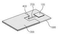
도 1은 본 발명에 따른 UWB용 칩 안테나의 일실시예를 나타내는 예시도 이고, 도 2는 본 발명에 따른 UWB용 칩 안테나의 일실시예의 3차원 구성을 도시하는 개략도, 도 3은 본 발명에 따른 UWB용 칩 안테나의 또 다른 일실시예를 나타내는 예시도 이다.1 is an exemplary view showing an embodiment of a UWB chip antenna according to the present invention, Figure 2 is a schematic diagram showing a three-dimensional configuration of one embodiment of a UWB chip antenna according to the present invention, Figure 3 is It is an exemplary view showing another embodiment of the chip antenna for UWB according to.
도 1과 도 2에 도시된 바와 같이, 본 발명에 따른 UWB용 칩 안테나는 다층 구조의 방사소자(100), 50 옴(ohm)의 마이크로 스트립 급전선로(200), 상판(Top GND) 및 하판(Bottom GND) 접지면(300), 급전용 비아(400), 유전체 기판(500) 및 더미 패드(Dummy Pad)(600)로 구성된다.As shown in FIG. 1 and FIG. 2, the UWB chip antenna according to the present invention has a multi-layered
이하에서는 유전체 기판(500)을 FR4 유전체를 적용한 경우를 기준으로 상세한 설명을 하나, 이는 상세한 설명의 수치 등을 쉽게 표현하기 위한 것일 뿐, 본 발명의 권리범위를 한정하기 위한 것이 아니다. 따라서 FR4 유전체와 균등한 유전체 또는 유사한 유전율 범위를 가지는 유전체를 이용한 경우에도, 본 발명의 권리범위에 포함되는 것은 자명할 것이다.Hereinafter, a detailed description will be made based on the case where the
방사소자(100)는 유전체 내부에 전극 패턴이 형성된 다층 구조를 가지고 있다. 즉, 상판 유전체(101)과 하판 유전체(103) 사이에 메탈로 이루어진 금속 패턴(200)을 끼운 적층구조인 것이 바람직하다.The
또한 방사소자(100)의 아래에 있는 FR4 기판(500)의 상판 접지면(Top GND)(301) 및 하판 접지면(Bottom GND)(302)를 제거함으로써, 방사소자(100)의 대역폭을 넓히는 것이 바람직하다.In addition, by removing the
방사소자(100)의 길이, 폭, 접지 면과의 간격 등에 의해 동작 주파수 내에서의 매칭 특성의 변동이 있기 때문에, 방사소자의 상판 및 하판은 유전율의 값이 15 이상 30 이하의 유전체를 사용하는 것이 안테나의 크기를 축소시킬 수 있다.Since there are variations in the matching characteristics within the operating frequency due to the length, width, and spacing of the
특히 유전율이 18일 경우, 이때의 방사소자(100)의 크기는 약 8.5㎜의 가로길이, 7.5 ㎜의 세로길이, 1.6 ㎜의 두께로 방사소자(100)를 구성할 수 있다.Particularly, when the dielectric constant is 18, the size of the
이러한 방사 소자는 Low Loss의 Cyclic Olefin Polymer (COP) based Composite을 이용하여 제작되도록 하는 것이 바람직하다.Such a radiating device is preferably made to use a low loss Cyclic Olefin Polymer (COP) based composite.
급전선로(Feeding Line)(200)는, 도 2에서 도시된 바와 같이, 하부 비아(402)를 통해 하판 접지면(Bottom GND)(302)에서 여기된 신호를 상기 방사소자(100)로 전달한다. 도 3에 도시된 실시예에 의한 경우에는, 또는 기판의 옆에서 여기된 신호를 상기 방사소자(100)로 전달한다.As shown in FIG. 2, the
이때, 급전선로(200)는 50 옴(ohm)의 특성 임피던스 값을 가지는 것이 바람직하다.In this case, the
접지면(300)은 상판 접지면(301)과 하판 접지면(302)을 포함한다.The
광대역 특성을 얻기 위하여, 상기 방사소자의 아랫부분에 위치하는 상판 접지면(Top GND)(301) 및 하판 접지면(Bottom GND)(302) 부분을 제거한 형태로 하는 것이 바람직하다.In order to obtain broadband characteristics, it is preferable to form the top ground (Top GND) 301 and bottom ground (Bottom GND) 302 portions that are disposed below the radiating element.
이때, 상판 접지면(Top GND)(301)은 디귿자(ㄷ) 형태로 하고, 상기 디귿자(ㄷ) 형태의 가운데에 위치하는 상기 급전선로(200)와 3 밀리미터의 거리로 이격된 것이 바람직하다.In this case, the top ground plane (Top GND) 301 is in the form of a d-shaped (c), it is preferable to be spaced apart from the
상판 접지면(Top GND)(301)은 광대역 특성을 얻기 위하여,상기 방사소자의 아랫부분에 위치하는 접지면 부분을 제거한 디귿자(ㄷ) 형태로 하는 것이 바람직하다. 이때, 상판 접지면(Top GND)(301)은, 상기 디귿자(ㄷ) 형태의 가운데에 위치하는 상기 급전선로(200)와 3 밀리미터의 거리로 이격된 것이 바람직하다.In order to obtain broadband characteristics, the top ground plane (Top GND) 301 is preferably in the form of a recess (C) having a portion of the ground plane positioned below the radiating element. At this time, the top ground plane (Top GND) (301) is preferably spaced apart by a distance of 3 millimeters to the
하판 접지면(Bottom GND)(302)는 직사각형 형태를 이루나, 상기 방사소 자(100)의 아래에 해당하는 부분에는 하판 접지면(302)이 존재하지 않는다. 즉, FR4 유전체 기판(500)과 방사소자(100) 사이에는 어떠한 접지면(301 또는 302)를 두지 않음으로써 고효율을 이끌어낼 수 있다.The bottom
급전용 비아(400)는 상부 비아(401)과 하부 비아(402)를 포함한다.Feeding via 400 includes an
급전용 상부 비아(401)는 상기 방사소자(100)와 상기 급전선로(200)를 연결하고, 급전용 하부 비아(402)는 상기 급전선로(200)와 상기 FR4 유전체 기판(500) 및 하판 접지면(302)을 연결한다.The
이때, 급전용 상부 비아(401)는 상기 방사소자의 금속 패턴(102)과 상기 급전선로(200)의 한쪽 끝 부분을 연결하고, 급전용 하부 비아(402)는 상기 급전선로(200)의 반대편 끝 부분과 상기 FR4 유전체 기판(500)의 중앙 및 상기 하부 접지면(302)을 연결하는 것이 바람직하다.In this case, the feed
FR4 유전체 기판(500)은 21 내지 23 밀리미터의 가로길이 및 38 내지 42 밀리미터의 세로길이를 가지는 직사각형 형태의 것이 바람직하며, 특히 가로 22 mm, 세로 40 mm의 크기를 가지는 것이 바람직하다. 이는 USB 동글(Dongle)의 크기와 유사하게 하기 위함이다.The FR4
이때, 방사소자(100) 아래의 FR4 유전체 기판(500) 위의 상판 접지면(Top GND)(301)을 제거한 형태(ㄷ자 형태)를 이용하여 FR4 유전체 기판(500)에 방사소자(100)가 위치하도록 함으로써 광대역 특성을 얻게 되며, 급전선로(200)의 길이도 최적의 매칭을 이루고 있다.At this time, the
더미 패드(600)는 방사소자(100)를 FR4 유전체 기판(500)에 붙이기 위한 납 땜용 패드이다.The
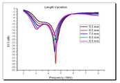
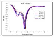
도 4a는 길이, 4b는 폭, 4c는 접지 면과의 간격에 따른 본 발명에 따른 칩 안테나의 성능을 시뮬레이션 한 결과를 나타내는 그래프이고, 도 5는 유전율이 4.5, 18, 30 일 때 시뮬레이션 한 본 발명에 따른 안테나의 반사손실의 특성을 나타내는 그래프이다.Figure 4a is a graph showing the results of the simulation of the chip antenna performance according to the length, 4b is the width, 4c is the distance to the ground plane, Figure 5 is a simulation simulated when the dielectric constant is 4.5, 18, 30 It is a graph showing the characteristics of the return loss of the antenna according to the invention.
방사소자(100)의 유전율에 따른 안테나 크기 변화에 중점적으로 이를 살펴보면, 먼저 FR4 유전체 기판(500)과 동일한 4.5의 유전율을 이용하여 방사소자(100)를 설계하게 되면(그래프에서의 삼각형 선) 전체 크기는 15.5 ㎜ * 5.7 ㎜가 되며, 이는 상기의 유전율을 18로 설계한 경우(그래프에서의 사각형 선)에 비해 약 25%의 크기 증가가 발생하게 된다.Focusing on the change in antenna size according to the dielectric constant of the
즉, 고유전율 소재를 적용하는 경우 안테나의 사이즈 감소효과를 얻을 수 있다.That is, when the high dielectric constant material is applied, the size reduction effect of the antenna can be obtained.
한편, 유전율이 30인 경우(그래프에서의 다이아몬드 선) 방사소자(100)의 사이즈 감소 효과는 크지 않으나 방사소자(100)의 두께를 줄이는 효과를 얻을 수 있다.On the other hand, if the dielectric constant is 30 (diamond line in the graph), the effect of reducing the size of the
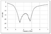
도 6은 네트워크 애널라이저 (Network Analyzer)를 이용하여 본 발명에 따른 칩 안테나의 반사손실을 측정한 결과를 도시하는 그래프이다.6 is a graph showing the results of measuring the return loss of the chip antenna according to the present invention using a network analyzer.
도시된 바와 같이, 3.1GHz 내지 5.2GHz 사이에 반사 손실은 약 10 dB 이상으 로 나타남을 알 수 있다.As shown, it can be seen that the reflection loss is represented by about 10 dB or more between 3.1 GHz and 5.2 GHz.
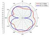
도 7은 본 발명에 따른 칩 안테나의 방사패턴을 나타내는 그래프이다.7 is a graph illustrating a radiation pattern of a chip antenna according to the present invention.
도 7a는 3GHz, 7b는 4GHz, 7c는 5GHz일 때의 E-field 및 H-field를 측정한 것을 도시하고 있다. 도시된 바와 같이, Omni-directional과 유사한 패턴이 형성됨을 알 수 있다. 또한 이때의 안테나 이득은 1.5 dBi 내지 4 dBi의 높은 안테나 이득 값을 보이고 있음을 알 수 있다.FIG. 7A shows measurements of the E-field and the H-field at 3 GHz, 7b at 4 GHz, and 7c at 5 GHz. As shown, it can be seen that a pattern similar to Omni-directional is formed. In addition, it can be seen that the antenna gain at this time shows a high antenna gain value of 1.5 dBi to 4 dBi.
이상에서와 같이 상세한 설명과 도면을 통해 본 발명의 실시 예를 설명하였다. 이러한 용어들은 단지 본 발명을 설명하기 위한 목적에서 사용된 것이지, 발명의 의미 한정이나 특허청구범위에 기재된 본 발명의 범위를 제한하기 위하여 사용된 것은 아니다.As described above, the embodiments of the present invention have been described through the detailed description and the drawings. These terms are only used for the purpose of describing the present invention, but are not used to limit the meaning of the invention or to limit the scope of the invention described in the claims.
따라서, 본 기술 분야의 통상의 지식을 가진 자라면 이로부터 다양한 변형 및 균등한 타 실시 예가 가능하다는 점을 이해할 것이며, 본 발명의 진정한 기술적 보호 범위는 첨부된 특허청구범위의 기술적 사상에 의해 정해져야 할 것이다.Therefore, those skilled in the art will understand that various modifications and equivalent other embodiments are possible from this, and the true technical protection scope of the present invention should be defined by the technical spirit of the appended claims. something to do.
도 1은 본 발명에 따른 UWB용 칩 안테나의 일실시예를 나타내는 예시도.1 is an exemplary view showing an embodiment of a UWB chip antenna according to the present invention.
도 2는 본 발명에 따른 UWB용 칩 안테나의 일실시예의 3차원 구성을 도시하는 개략도.Figure 2 is a schematic diagram showing a three-dimensional configuration of one embodiment of a chip antenna for UWB according to the present invention.
도 3은 본 발명에 따른 UWB용 칩 안테나의 또 다른 일실시예를 나타내는 예시도.Figure 3 is an exemplary view showing another embodiment of a chip antenna for UWB according to the present invention.
도 4a는 길이, 4b는 폭, 4c는 접지 면과의 간격에 따른 본 발명에 따른 칩 안테나의 성능을 시뮬레이션 한 결과를 나타내는 그래프.Figure 4a is a graph showing the results of simulating the performance of the chip antenna according to the present invention according to the length, 4b is the width, 4c is the distance to the ground plane.
도 5는 유전율이 4.5, 18, 30 일 때 시뮬레이션 한 본 발명에 따른 안테나의 반사손실의 특성을 나타내는 그래프.5 is a graph showing the characteristics of the return loss of the antenna according to the present invention simulated when the dielectric constant is 4.5, 18, 30.
도 6은 네트워크 애널라이저 (Network Analyzer)를 이용하여 본 발명에 따른 칩 안테나의 반사손실을 측정한 결과를 도시하는 그래프.6 is a graph showing the results of measuring the return loss of the chip antenna according to the present invention using a network analyzer.
도 7은 본 발명에 따른 칩 안테나의 방사패턴을 나타내는 그래프.7 is a graph showing a radiation pattern of the chip antenna according to the present invention.
Claims (12)
Translated fromKoreanPriority Applications (1)
| Application Number | Priority Date | Filing Date | Title |
|---|---|---|---|
| KR1020070140098AKR100980779B1 (en) | 2007-12-28 | 2007-12-28 | Consumer Chip Antenna |
Applications Claiming Priority (1)
| Application Number | Priority Date | Filing Date | Title |
|---|---|---|---|
| KR1020070140098AKR100980779B1 (en) | 2007-12-28 | 2007-12-28 | Consumer Chip Antenna |
Publications (2)
| Publication Number | Publication Date |
|---|---|
| KR20090072100Atrue KR20090072100A (en) | 2009-07-02 |
| KR100980779B1 KR100980779B1 (en) | 2010-09-10 |
Family
ID=41329363
Family Applications (1)
| Application Number | Title | Priority Date | Filing Date |
|---|---|---|---|
| KR1020070140098AExpired - Fee RelatedKR100980779B1 (en) | 2007-12-28 | 2007-12-28 | Consumer Chip Antenna |
Country Status (1)
| Country | Link |
|---|---|
| KR (1) | KR100980779B1 (en) |
Cited By (6)
| Publication number | Priority date | Publication date | Assignee | Title |
|---|---|---|---|---|
| CN102509869A (en)* | 2011-10-11 | 2012-06-20 | 北京邮电大学 | Micro-strip gradually-changing-slot antenna |
| CN108370088A (en)* | 2015-12-15 | 2018-08-03 | Lg伊诺特有限公司 | Electronic shelf label and antenna for electronic shelf label |
| CN110011039A (en)* | 2017-11-29 | 2019-07-12 | Tdk株式会社 | Paster antenna |
| KR20190105812A (en)* | 2018-03-06 | 2019-09-18 | 동우 화인켐 주식회사 | Film antenna and display device including the same |
| KR20200108820A (en)* | 2018-03-06 | 2020-09-21 | 동우 화인켐 주식회사 | Film antenna and display device including the same |
| WO2022019561A1 (en)* | 2020-07-21 | 2022-01-27 | 동우화인켐 주식회사 | Antenna element and display device comprising same |
Family Cites Families (4)
| Publication number | Priority date | Publication date | Assignee | Title |
|---|---|---|---|---|
| KR100416885B1 (en)* | 2001-07-27 | 2004-02-05 | (주)신아정보통신 | Small antenna of wireless data communication |
| JP2004140496A (en) | 2002-10-16 | 2004-05-13 | Taiyo Yuden Co Ltd | Dielectric antenna and mobile communication equipment containing the same |
| JP2006217047A (en)* | 2005-02-01 | 2006-08-17 | Chant Sincere Co Ltd | Method for manufacturing microchip antenna |
| KR100707242B1 (en)* | 2005-02-25 | 2007-04-13 | 한국정보통신대학교 산학협력단 | Dielectric chip antenna |
- 2007
- 2007-12-28KRKR1020070140098Apatent/KR100980779B1/ennot_activeExpired - Fee Related
Cited By (10)
| Publication number | Priority date | Publication date | Assignee | Title |
|---|---|---|---|---|
| CN102509869A (en)* | 2011-10-11 | 2012-06-20 | 北京邮电大学 | Micro-strip gradually-changing-slot antenna |
| CN102509869B (en)* | 2011-10-11 | 2014-03-19 | 北京邮电大学 | Micro-strip gradually-changing-slot antenna |
| CN108370088A (en)* | 2015-12-15 | 2018-08-03 | Lg伊诺特有限公司 | Electronic shelf label and antenna for electronic shelf label |
| US10607512B2 (en) | 2015-12-15 | 2020-03-31 | Atec Ap Co., Ltd. | Communication device and electronic device comprising the same |
| CN108370088B (en)* | 2015-12-15 | 2021-04-13 | 艾泰克Ap有限公司 | Communication device and electronic device including the same |
| CN110011039A (en)* | 2017-11-29 | 2019-07-12 | Tdk株式会社 | Paster antenna |
| KR20190105812A (en)* | 2018-03-06 | 2019-09-18 | 동우 화인켐 주식회사 | Film antenna and display device including the same |
| KR20200108820A (en)* | 2018-03-06 | 2020-09-21 | 동우 화인켐 주식회사 | Film antenna and display device including the same |
| US11316264B2 (en) | 2018-03-06 | 2022-04-26 | Dongwoo Fine-Chem Co., Ltd. | Antenna device and display device comprising the same |
| WO2022019561A1 (en)* | 2020-07-21 | 2022-01-27 | 동우화인켐 주식회사 | Antenna element and display device comprising same |
Also Published As
| Publication number | Publication date |
|---|---|
| KR100980779B1 (en) | 2010-09-10 |
Similar Documents
| Publication | Publication Date | Title |
|---|---|---|
| US8994593B2 (en) | Near-closed polygonal chain microstrip antenna | |
| KR20110129452A (en) | Balanced meta material antenna device | |
| JP2010063017A (en) | Rfid tag, rfid tag set and rfid system | |
| CN203503788U (en) | Microstrip antenna | |
| KR100980779B1 (en) | Consumer Chip Antenna | |
| CN101071901A (en) | Multi frequency antenna | |
| US7742001B2 (en) | Two-tier wide band antenna | |
| US7911390B2 (en) | Antenna structure | |
| WO2024125010A1 (en) | Compact ceramic chip antenna array based on ultra-wideband three-dimensional direction finding | |
| CN106099365A (en) | Weak coupling ultrabroad band mimo antenna | |
| CN206432384U (en) | Multi-input multi-output antenna system and mobile terminal | |
| CN206370497U (en) | A kind of broad-band antenna | |
| US8593368B2 (en) | Multi-band antenna and electronic apparatus having the same | |
| CN102270781B (en) | slot antenna | |
| TW201015782A (en) | Multi-frequency antenna and an electronic device having the multi-frequency antenna thereof | |
| CN103794868A (en) | Antenna assembly | |
| TW200847524A (en) | A miniaturized three-frequency rhombus coplanar waveguide antenna | |
| US9929462B2 (en) | Multiple layer dielectric panel directional antenna | |
| CN2770115Y (en) | Planar inverted F shaped antenna | |
| Gummalla et al. | Compact dual-band planar metamaterial antenna arrays for wireless LAN | |
| CN203456593U (en) | Dual-band slot antenna based on half-mode substrate integrated waveguide | |
| CN106025510A (en) | Antenna | |
| CN102800948B (en) | Antenna and wireless communication apparatus | |
| CN202217784U (en) | dual frequency antenna | |
| US7872606B1 (en) | Compact ultra wideband microstrip resonating antenna |
Legal Events
| Date | Code | Title | Description |
|---|---|---|---|
| A201 | Request for examination | ||
| PA0109 | Patent application | St.27 status event code:A-0-1-A10-A12-nap-PA0109 | |
| PA0201 | Request for examination | St.27 status event code:A-1-2-D10-D11-exm-PA0201 | |
| P11-X000 | Amendment of application requested | St.27 status event code:A-2-2-P10-P11-nap-X000 | |
| P13-X000 | Application amended | St.27 status event code:A-2-2-P10-P13-nap-X000 | |
| R15-X000 | Change to inventor requested | St.27 status event code:A-3-3-R10-R15-oth-X000 | |
| R16-X000 | Change to inventor recorded | St.27 status event code:A-3-3-R10-R16-oth-X000 | |
| D13-X000 | Search requested | St.27 status event code:A-1-2-D10-D13-srh-X000 | |
| D14-X000 | Search report completed | St.27 status event code:A-1-2-D10-D14-srh-X000 | |
| PG1501 | Laying open of application | St.27 status event code:A-1-1-Q10-Q12-nap-PG1501 | |
| E902 | Notification of reason for refusal | ||
| PE0902 | Notice of grounds for rejection | St.27 status event code:A-1-2-D10-D21-exm-PE0902 | |
| AMND | Amendment | ||
| E13-X000 | Pre-grant limitation requested | St.27 status event code:A-2-3-E10-E13-lim-X000 | |
| P11-X000 | Amendment of application requested | St.27 status event code:A-2-2-P10-P11-nap-X000 | |
| P13-X000 | Application amended | St.27 status event code:A-2-2-P10-P13-nap-X000 | |
| E601 | Decision to refuse application | ||
| PE0601 | Decision on rejection of patent | St.27 status event code:N-2-6-B10-B15-exm-PE0601 | |
| J201 | Request for trial against refusal decision | ||
| PJ0201 | Trial against decision of rejection | St.27 status event code:A-3-3-V10-V11-apl-PJ0201 | |
| AMND | Amendment | ||
| E13-X000 | Pre-grant limitation requested | St.27 status event code:A-2-3-E10-E13-lim-X000 | |
| P11-X000 | Amendment of application requested | St.27 status event code:A-2-2-P10-P11-nap-X000 | |
| P13-X000 | Application amended | St.27 status event code:A-2-2-P10-P13-nap-X000 | |
| PB0901 | Examination by re-examination before a trial | St.27 status event code:A-6-3-E10-E12-rex-PB0901 | |
| B701 | Decision to grant | ||
| PB0701 | Decision of registration after re-examination before a trial | St.27 status event code:A-3-4-F10-F13-rex-PB0701 | |
| GRNT | Written decision to grant | ||
| PR0701 | Registration of establishment | St.27 status event code:A-2-4-F10-F11-exm-PR0701 | |
| PR1002 | Payment of registration fee | St.27 status event code:A-2-2-U10-U11-oth-PR1002 Fee payment year number:1 | |
| PG1601 | Publication of registration | St.27 status event code:A-4-4-Q10-Q13-nap-PG1601 | |
| PN2301 | Change of applicant | St.27 status event code:A-5-5-R10-R13-asn-PN2301 St.27 status event code:A-5-5-R10-R11-asn-PN2301 | |
| FPAY | Annual fee payment | Payment date:20130621 Year of fee payment:4 | |
| PR1001 | Payment of annual fee | St.27 status event code:A-4-4-U10-U11-oth-PR1001 Fee payment year number:4 | |
| LAPS | Lapse due to unpaid annual fee | ||
| PC1903 | Unpaid annual fee | St.27 status event code:A-4-4-U10-U13-oth-PC1903 Not in force date:20140902 Payment event data comment text:Termination Category : DEFAULT_OF_REGISTRATION_FEE | |
| PC1903 | Unpaid annual fee | St.27 status event code:N-4-6-H10-H13-oth-PC1903 Ip right cessation event data comment text:Termination Category : DEFAULT_OF_REGISTRATION_FEE Not in force date:20140902 | |
| P22-X000 | Classification modified | St.27 status event code:A-4-4-P10-P22-nap-X000 | |
| R18-X000 | Changes to party contact information recorded | St.27 status event code:A-5-5-R10-R18-oth-X000 | |
| PN2301 | Change of applicant | St.27 status event code:A-5-5-R10-R13-asn-PN2301 St.27 status event code:A-5-5-R10-R11-asn-PN2301 | |
| PN2301 | Change of applicant | St.27 status event code:A-5-5-R10-R13-asn-PN2301 St.27 status event code:A-5-5-R10-R11-asn-PN2301 |