KR20090068020A - Gate forming method of a nonvolatile memory device having a charge trap layer - Google Patents
Gate forming method of a nonvolatile memory device having a charge trap layerDownload PDFInfo
- Publication number
- KR20090068020A KR20090068020AKR1020070135871AKR20070135871AKR20090068020AKR 20090068020 AKR20090068020 AKR 20090068020AKR 1020070135871 AKR1020070135871 AKR 1020070135871AKR 20070135871 AKR20070135871 AKR 20070135871AKR 20090068020 AKR20090068020 AKR 20090068020A
- Authority
- KR
- South Korea
- Prior art keywords
- layer
- film
- gate
- charge trap
- forming
- Prior art date
- Legal status (The legal status is an assumption and is not a legal conclusion. Google has not performed a legal analysis and makes no representation as to the accuracy of the status listed.)
- Ceased
Links
- 238000000034methodMethods0.000titleclaimsabstractdescription52
- 238000005530etchingMethods0.000claimsabstractdescription17
- 230000005641tunnelingEffects0.000claimsabstractdescription16
- 230000000903blocking effectEffects0.000claimsabstractdescription12
- 239000004065semiconductorSubstances0.000claimsabstractdescription9
- 239000000758substrateSubstances0.000claimsabstractdescription7
- 229910052581Si3N4Inorganic materials0.000claimsdescription13
- HQVNEWCFYHHQES-UHFFFAOYSA-Nsilicon nitrideChemical compoundN12[Si]34N5[Si]62N3[Si]51N64HQVNEWCFYHHQES-UHFFFAOYSA-N0.000claimsdescription13
- 230000001590oxidative effectEffects0.000claimsdescription9
- XUIMIQQOPSSXEZ-UHFFFAOYSA-NSiliconChemical compound[Si]XUIMIQQOPSSXEZ-UHFFFAOYSA-N0.000claimsdescription7
- 229910052710siliconInorganic materials0.000claimsdescription7
- 239000010703siliconSubstances0.000claimsdescription7
- WFKWXMTUELFFGS-UHFFFAOYSA-NtungstenChemical compound[W]WFKWXMTUELFFGS-UHFFFAOYSA-N0.000claimsdescription7
- 229910052721tungstenInorganic materials0.000claimsdescription7
- 239000010937tungstenSubstances0.000claimsdescription7
- XKRFYHLGVUSROY-UHFFFAOYSA-NArgonChemical compound[Ar]XKRFYHLGVUSROY-UHFFFAOYSA-N0.000claimsdescription6
- 238000004519manufacturing processMethods0.000claimsdescription6
- 229910021420polycrystalline siliconInorganic materials0.000claimsdescription6
- 229920005591polysiliconPolymers0.000claimsdescription6
- 239000001301oxygenSubstances0.000claimsdescription5
- 229910052760oxygenInorganic materials0.000claimsdescription5
- MZLGASXMSKOWSE-UHFFFAOYSA-Ntantalum nitrideChemical compound[Ta]#NMZLGASXMSKOWSE-UHFFFAOYSA-N0.000claimsdescription5
- KJTLSVCANCCWHF-UHFFFAOYSA-NRutheniumChemical compound[Ru]KJTLSVCANCCWHF-UHFFFAOYSA-N0.000claimsdescription4
- NRTOMJZYCJJWKI-UHFFFAOYSA-NTitanium nitrideChemical compound[Ti]#NNRTOMJZYCJJWKI-UHFFFAOYSA-N0.000claimsdescription4
- IVHJCRXBQPGLOV-UHFFFAOYSA-NazanylidynetungstenChemical compound[W]#NIVHJCRXBQPGLOV-UHFFFAOYSA-N0.000claimsdescription4
- 229910052707rutheniumInorganic materials0.000claimsdescription4
- WNUPENMBHHEARK-UHFFFAOYSA-Nsilicon tungstenChemical compound[Si].[W]WNUPENMBHHEARK-UHFFFAOYSA-N0.000claimsdescription4
- 229910052786argonInorganic materials0.000claimsdescription3
- QVGXLLKOCUKJST-UHFFFAOYSA-Natomic oxygenChemical compound[O]QVGXLLKOCUKJST-UHFFFAOYSA-N0.000claimsdescription3
- 239000001307heliumSubstances0.000claimsdescription3
- 229910052734heliumInorganic materials0.000claimsdescription3
- SWQJXJOGLNCZEY-UHFFFAOYSA-Nhelium atomChemical compound[He]SWQJXJOGLNCZEY-UHFFFAOYSA-N0.000claimsdescription3
- 239000001257hydrogenSubstances0.000claimsdescription3
- 229910052739hydrogenInorganic materials0.000claimsdescription3
- 125000004435hydrogen atomChemical class[H]*0.000claimsdescription3
- 230000008569processEffects0.000abstractdescription33
- 230000002542deteriorative effectEffects0.000abstractdescription4
- 238000007254oxidation reactionMethods0.000description11
- 230000003647oxidationEffects0.000description8
- 238000000059patterningMethods0.000description5
- 239000004020conductorSubstances0.000description3
- 238000001312dry etchingMethods0.000description3
- 230000014759maintenance of locationEffects0.000description3
- 239000000463materialSubstances0.000description3
- 238000004140cleaningMethods0.000description2
- 230000007423decreaseEffects0.000description2
- 230000010354integrationEffects0.000description2
- 238000003860storageMethods0.000description2
- 229910018072Al 2 O 3Inorganic materials0.000description1
- 230000002411adverseEffects0.000description1
- MIQVEZFSDIJTMW-UHFFFAOYSA-Naluminum hafnium(4+) oxygen(2-)Chemical compound[O-2].[Al+3].[Hf+4]MIQVEZFSDIJTMW-UHFFFAOYSA-N0.000description1
- 238000000137annealingMethods0.000description1
- 239000006227byproductSubstances0.000description1
- 230000008878couplingEffects0.000description1
- 238000010168coupling processMethods0.000description1
- 238000005859coupling reactionMethods0.000description1
- 230000001351cycling effectEffects0.000description1
- 230000007547defectEffects0.000description1
- 230000006870functionEffects0.000description1
- CJNBYAVZURUTKZ-UHFFFAOYSA-Nhafnium(iv) oxideChemical compoundO=[Hf]=OCJNBYAVZURUTKZ-UHFFFAOYSA-N0.000description1
- 230000035876healingEffects0.000description1
- 238000010438heat treatmentMethods0.000description1
- 239000012535impuritySubstances0.000description1
- 238000002955isolationMethods0.000description1
- 229910052751metalInorganic materials0.000description1
- 239000002184metalSubstances0.000description1
- 238000012986modificationMethods0.000description1
- 230000004048modificationEffects0.000description1
- 150000004767nitridesChemical class0.000description1
- TWNQGVIAIRXVLR-UHFFFAOYSA-Noxo(oxoalumanyloxy)alumaneChemical compoundO=[Al]O[Al]=OTWNQGVIAIRXVLR-UHFFFAOYSA-N0.000description1
- 239000000047productSubstances0.000description1
- 230000001681protective effectEffects0.000description1
- 230000009467reductionEffects0.000description1
- WQJQOUPTWCFRMM-UHFFFAOYSA-Ntungsten disilicideChemical compound[Si]#[W]#[Si]WQJQOUPTWCFRMM-UHFFFAOYSA-N0.000description1
- 229910021342tungsten silicideInorganic materials0.000description1
- 238000009279wet oxidation reactionMethods0.000description1
Images

Classifications
- H—ELECTRICITY
- H10—SEMICONDUCTOR DEVICES; ELECTRIC SOLID-STATE DEVICES NOT OTHERWISE PROVIDED FOR
- H10B—ELECTRONIC MEMORY DEVICES
- H10B43/00—EEPROM devices comprising charge-trapping gate insulators
- H10B43/30—EEPROM devices comprising charge-trapping gate insulators characterised by the memory core region
- H—ELECTRICITY
- H01—ELECTRIC ELEMENTS
- H01L—SEMICONDUCTOR DEVICES NOT COVERED BY CLASS H10
- H01L21/00—Processes or apparatus adapted for the manufacture or treatment of semiconductor or solid state devices or of parts thereof
- H01L21/02—Manufacture or treatment of semiconductor devices or of parts thereof
- H01L21/02104—Forming layers
- H01L21/02107—Forming insulating materials on a substrate
- H01L21/02225—Forming insulating materials on a substrate characterised by the process for the formation of the insulating layer
- H01L21/02227—Forming insulating materials on a substrate characterised by the process for the formation of the insulating layer formation by a process other than a deposition process
- H01L21/02252—Forming insulating materials on a substrate characterised by the process for the formation of the insulating layer formation by a process other than a deposition process formation by plasma treatment, e.g. plasma oxidation of the substrate
- H—ELECTRICITY
- H10—SEMICONDUCTOR DEVICES; ELECTRIC SOLID-STATE DEVICES NOT OTHERWISE PROVIDED FOR
- H10B—ELECTRONIC MEMORY DEVICES
- H10B41/00—Electrically erasable-and-programmable ROM [EEPROM] devices comprising floating gates
- H10B41/30—Electrically erasable-and-programmable ROM [EEPROM] devices comprising floating gates characterised by the memory core region
- H—ELECTRICITY
- H10—SEMICONDUCTOR DEVICES; ELECTRIC SOLID-STATE DEVICES NOT OTHERWISE PROVIDED FOR
- H10B—ELECTRONIC MEMORY DEVICES
- H10B69/00—Erasable-and-programmable ROM [EPROM] devices not provided for in groups H10B41/00 - H10B63/00, e.g. ultraviolet erasable-and-programmable ROM [UVEPROM] devices
- H—ELECTRICITY
- H10—SEMICONDUCTOR DEVICES; ELECTRIC SOLID-STATE DEVICES NOT OTHERWISE PROVIDED FOR
- H10D—INORGANIC ELECTRIC SEMICONDUCTOR DEVICES
- H10D30/00—Field-effect transistors [FET]
- H10D30/01—Manufacture or treatment
- H10D30/021—Manufacture or treatment of FETs having insulated gates [IGFET]
- H10D30/0413—Manufacture or treatment of FETs having insulated gates [IGFET] of FETs having charge-trapping gate insulators, e.g. MNOS transistors
- H—ELECTRICITY
- H10—SEMICONDUCTOR DEVICES; ELECTRIC SOLID-STATE DEVICES NOT OTHERWISE PROVIDED FOR
- H10D—INORGANIC ELECTRIC SEMICONDUCTOR DEVICES
- H10D64/00—Electrodes of devices having potential barriers
- H10D64/60—Electrodes characterised by their materials
- H10D64/66—Electrodes having a conductor capacitively coupled to a semiconductor by an insulator, e.g. MIS electrodes
- H10D64/68—Electrodes having a conductor capacitively coupled to a semiconductor by an insulator, e.g. MIS electrodes characterised by the insulator, e.g. by the gate insulator
- H10D64/691—Electrodes having a conductor capacitively coupled to a semiconductor by an insulator, e.g. MIS electrodes characterised by the insulator, e.g. by the gate insulator comprising metallic compounds, e.g. metal oxides or metal silicates
Landscapes
- Engineering & Computer Science (AREA)
- Physics & Mathematics (AREA)
- Plasma & Fusion (AREA)
- Condensed Matter Physics & Semiconductors (AREA)
- General Physics & Mathematics (AREA)
- Manufacturing & Machinery (AREA)
- Computer Hardware Design (AREA)
- Microelectronics & Electronic Packaging (AREA)
- Power Engineering (AREA)
- Semiconductor Memories (AREA)
- Non-Volatile Memory (AREA)
Abstract
Translated fromKoreanDescription
Translated fromKorean본 발명은 불휘발성 메모리소자의 제조방법에 관한 것으로서, 특히 전하트랩층을 갖는 불휘발성 메모리소자의 게이트 형성방법에 관한 것이다.The present invention relates to a method of manufacturing a nonvolatile memory device, and more particularly, to a method of forming a gate of a nonvolatile memory device having a charge trap layer.
일반적으로, 데이터를 저장하기 위해 사용되는 반도체 메모리소자는 휘발성(volatile) 메모리소자와 불휘발성(non-volatile) 메모리소자로 구별될 수 있다. 휘발성 메모리소자는 전원 공급이 중단됨에 따라 저장된 데이터가 소실되지만, 불휘발성 메모리소자는 전원 공급이 중단되더라도 저장된 데이터가 유지된다. 따라서 이동전화시스템, 음악 및/또는 영상 데이터를 저장하기 위한 메모리카드 및 그 밖의 다른 응용 장치에서와 같이, 전원을 항상 사용할 수 없거나 종종 중단되거나, 또는 낮은 파워 사용이 요구되는 상황에서는 불휘발성 메모리소자가 폭넓게 사용된다. 이와 같은 불휘발성 메모리소자의 대표적인 예가 일괄 소거가 가능한 플래시(flash) 메모리이다.In general, semiconductor memory devices used to store data can be classified into volatile memory devices and non-volatile memory devices. In the volatile memory device, the stored data is lost when the power supply is interrupted, but in the nonvolatile memory device, the stored data is maintained even when the power supply is interrupted. Thus, such as in mobile phone systems, memory cards and other applications for storing music and / or video data, nonvolatile memory devices in situations where power is not always available, often interrupted, or where low power usage is required. Is widely used. A typical example of such a nonvolatile memory device is a flash memory capable of batch erasing.
플래시 메모리소자의 셀 트랜지스터는, 일반적인 불휘발성 메모리소자와 마찬가지로 적층된 게이트(stacked gate) 구조를 갖는 것이 대표적이다. 적층된 게이 트 구조의 대표적인 것이 폴리실리콘막을 아이피오(IPO; Inter-Poly Oxide)로 캡핑(capping)하고 있는 플로팅게이트형 구조이다. 플로팅게이트형 플래시 메모리소자는 확장성(extendibility)이 우수하여 최근에는 멀티 레벨 칩(multi-level chip)까지 개발이 진행되고 있다. 그러나, 최근에는 플로팅게이트를 적용한 플래시 메모리소자의 고집적화가 급격히 이루어짐에 따라, 인접 셀의 차지(charge) 상태에 따라 문턱전압이 급격하게 변화되는 상호간섭(interference) 또는 커플링(coupling) 문제가 심각하게 대두되고 있다. 따라서, 이러한 인접 셀 간의 상호간섭을 극복하기 위한 새로운 셀 구조에 대한 시도가 이루어지고 있다.A cell transistor of a flash memory device typically has a stacked gate structure like a general nonvolatile memory device. A representative gate stacked structure is a floating gate structure in which a polysilicon film is capped with IPO (Inter-Poly Oxide). Floating gate type flash memory devices are excellent in extensibility and have recently been developed to multi-level chips. However, as the integration of flash memory devices using floating gates has recently been rapidly integrated, there has been a serious problem of interference or coupling, in which threshold voltages are rapidly changed depending on charge states of adjacent cells. Is emerging. Thus, attempts have been made for a new cell structure to overcome such interference between adjacent cells.
최근에는 집적도가 증가하더라도 셀 간에 간섭현상이 덜 발생하는 전하트랩층(charge trapping layer)을 갖는 불휘발성 메모리소자에 대한 관심이 증대되고 있다. 전하트랩층을 갖는 불휘발성 메모리소자는, 채널영역을 갖는 기판 상에 터널링층(tunneling layer), 전하트랩층, 블로킹층(blocking layer) 및 컨트롤게이트전극이 순차적으로 적층된 구조를 갖는 것이 일반적이다.Recently, interest in nonvolatile memory devices having a charge trapping layer having less interference between cells even though the degree of integration has increased has increased. In general, a nonvolatile memory device having a charge trap layer has a structure in which a tunneling layer, a charge trap layer, a blocking layer, and a control gate electrode are sequentially stacked on a substrate having a channel region. .
한편, 반도체 메모리소자의 디자인 룰(design rule)이 점차 미세해지면서 게이트 패턴을 형성하기 위한 식각공정이 더욱 어려워지고 있다. 예컨대 전하트랩형 불휘발성 메모리소자에서 게이트 구조를 형성하기 위해서는 반도체기판 상에 터널링층, 전하트랩층, 블로킹층 및 컨트롤게이트 전극층을 차례로 적층한 후, 디자인 룰에 따라 적층 막들을 요구하는 스케일로 패터닝하는 공정이 필수적이다. 이러한 패터닝공정은 통상 높은 에너지를 사용하는 건식식각 공정으로 이루어지는데, 이 과정에서 게이트 구조를 이루고 있는 여러 막들이 손상(damage)을 입게 된다. 특 히, 전하트랩층과 터널링층의 가장자리 부분에 이러한 손상이 집중될 수 있다.On the other hand, as the design rules of semiconductor memory devices become increasingly finer, etching processes for forming gate patterns become more difficult. For example, in order to form a gate structure in a charge trapping nonvolatile memory device, a tunneling layer, a charge trap layer, a blocking layer, and a control gate electrode layer are sequentially stacked on a semiconductor substrate, and then patterned on a scale requiring stacking layers according to design rules. The process is essential. The patterning process is usually a dry etching process using high energy, and in this process, various films forming the gate structure are damaged. In particular, this damage can be concentrated on the edges of the charge trap layer and the tunneling layer.
전하트랩형 불휘발성 메모리소자에서, 프로그램 또는 소거 동작과 같은 동작들이 반복적으로 이루어지는 싸이클링(cycling)에서 전하트랩층에 트랩된 전자들이 인접 셀 또는 상부로 누설되지 않도록 하는 전하저장특성, 즉 리텐션(retention)은 소자의 특성을 결정하는 중요한 요소가 되고 있다. 프로그램 동작에 의해 전하트랩층에 트랩된 전자가 읽기동작을 수행하는 동안 인접 셀로 이동하게 되면 메모리 셀의 문턱전압이 변화하게 되고 결국 소자의 불량이 발생하는 것이다. 게이트 패터닝 과정에서 발생한 전하트랩층 또는 터널링층의 손상은 전하(charge) 손실을 유발하므로, 게이트 패터닝 공정 후 열처리 등을 통하여 이러한 손상을 회복시키는 공정이 수반된다.In a charge trapping nonvolatile memory device, a charge storage characteristic, that is, retention, is performed so that electrons trapped in the charge trap layer are not leaked to an adjacent cell or upper part in a cycling in which operations such as a program or erase operation are repeatedly performed. Retention is becoming an important factor in determining device characteristics. When electrons trapped in the charge trap layer move to an adjacent cell during the read operation by the program operation, the threshold voltage of the memory cell is changed, resulting in device defects. Since the damage of the charge trap layer or the tunneling layer generated during the gate patterning process causes charge loss, a process of recovering such damage through heat treatment after the gate patterning process is involved.
최근에는 디자인 룰의 감소에 따라 게이트의 선폭이 작아지면서 발생하는 저항문제를 해결하기 위하여, 기존의 폴리실리콘이나 텅스텐 실리사이드(WSi) 외에 텅스텐(W), 티타늄나이트라이드(TiN), 탄탈륨나이트라이드(TaN), 루테늄(Ru)과 같은 새로운 저저항 게이트물질을 사용하게 되었다. 이에 따라, 게이트 식각 공정의 난이도는 급격하게 높아지고, 식각공정에서 발생한 손상(damage)을 치유하기 위한 공정은 더욱 까다로워졌다. 게이트 식각공정에서 발생한 손상을 치유하는 방법으로 널리 사용되는 것은, 고온의 플라즈마를 이용하여 게이트 패턴의 측벽을 산화시키는 방법이다. 그러나, 새롭게 사용되는 상기 저저항 게이트 도전체들은 산화반응이 매우 빠르게 일어나기 때문에, 고온 플라즈마 산화방법을 적용할 경우 손상된 부분만 선택적으로 산화시키기가 매우 어렵다. 특히, 텅스텐(W)을 게이트 도전체로 사 용할 경우에는 텅스텐(W)의 산화반응이 너무 쉽게 일어나기 때문에 실리콘나이트라이드를 보호막으로 사용하기도 하지만 게이트의 특성을 열화시키는 문제점이 있다.Recently, in order to solve the resistance problem caused by the decrease in the gate width as the design rule decreases, tungsten (W), titanium nitride (TiN), tantalum nitride (in addition to polysilicon or tungsten silicide (WSi)) New low resistance gate materials such as TaN) and ruthenium (Ru) are used. Accordingly, the difficulty of the gate etching process is sharply increased, and the process for healing the damage generated in the etching process is more difficult. Widely used as a method of curing damages generated in the gate etching process, a sidewall of the gate pattern is oxidized using a high temperature plasma. However, the newly used low resistance gate conductors have a very rapid oxidation reaction, and therefore, it is very difficult to selectively oxidize only the damaged part when the high temperature plasma oxidation method is applied. In particular, when tungsten (W) is used as the gate conductor, since the oxidation reaction of tungsten (W) occurs so easily, silicon nitride may be used as a protective film, but there is a problem of deteriorating the characteristics of the gate.
본 발명이 이루고자 하는 기술적 과제는, 소자의 특성을 열화시키지 않으면서 게이트 식각공정에서 발생한 식각 손상을 제거할 수 있는 불휘발성 메모리소자의 게이트 형성방법을 제공하는 데 있다.It is an object of the present invention to provide a method of forming a gate of a nonvolatile memory device capable of eliminating etch damage generated in a gate etching process without deteriorating device characteristics.
상기 기술적 과제를 이루기 위하여 본 발명에 따른 불휘발성 메모리소자의 게이트 형성방법은, 반도체기판 상에 터널링층, 전하트랩층, 블로킹층 및 컨트롤게이트층을 형성하는 단계와, 컨트롤게이트층 상에, 게이트가 형성될 영역을 한정하는 하드마스크를 형성하는 단계와, 하드마스크를 식각 마스크로 사용하여 컨트롤게이트층, 블로킹층, 전하트랩층 및 터널링층을 식각하여 게이트 패턴을 형성하는 단계, 및 1 ∼ 10mT의 초저압 플라즈마를 이용하여 게이트 패턴의 측면에 식각보상막을 형성하는 단계를 포함하는 것을 특징으로 한다.According to an aspect of the present invention, there is provided a method of forming a gate of a nonvolatile memory device, the method including: forming a tunneling layer, a charge trap layer, a blocking layer, and a control gate layer on a semiconductor substrate; Forming a hard mask defining a region to be formed, etching the control gate layer, the blocking layer, the charge trap layer, and the tunneling layer using the hard mask as an etching mask, and forming a gate pattern, and 1 to 10 mT. Forming an etch compensation film on the side of the gate pattern using the ultra-low pressure plasma of the.
상기 컨트롤게이트층은 폴리실리콘막, 텅스텐(W)막, 텅스텐실리사이드(WSi)막, 텅스텐나이트라이드(WN)막, 탄탈륨나이트라이드(TaN)막, 티타늄나이트라이드(TiN), 루테늄(Ru) 중의 어느 하나 또는 둘 이상의 적층막으로 형성할 수 있다.The control gate layer is formed of a polysilicon film, a tungsten (W) film, a tungsten silicide (WSi) film, a tungsten nitride (WN) film, a tantalum nitride (TaN) film, titanium nitride (TiN), or ruthenium (Ru). It may be formed of any one or two or more laminated films.
상기 식각보상막을 형성하는 단계는 고밀도 플라즈마(HDP) 방식을 이용하여 상기 게이트 패턴의 측면을 산화시키는 단계를 포함할 수 있다.The forming of the etch compensation layer may include oxidizing side surfaces of the gate pattern using a high density plasma (HDP) method.
상기 게이트 패턴의 측면을 산화시키는 단계는, 1 ∼ 100mT의 압력과, 200 ∼ 500℃의 온도에서 실시할 수 있다.The step of oxidizing the side surface of the gate pattern may be carried out at a pressure of 1 ~ 100mT, and a temperature of 200 ~ 500 ℃.
상기 게이트 패턴의 측면을 산화시키는 단계는 산소(O2), 헬륨(He), 아르곤(Ar) 또는 수소(H2) 중의 어느 하나 또는 둘 이상을 조합하여 사용하여 수행할 수 있다.The step of oxidizing the side surface of the gate pattern may be performed using any one or two or more of oxygen (O2 ), helium (He), argon (Ar), or hydrogen (H2 ) in combination.
상기 게이트 패턴의 측면을 산화시키는 단계에서, 상기 게이트 패턴 측면에 10 ∼ 100Å의 산화막이 형성되도록 하는 것이 바람직하다.In the step of oxidizing the side surface of the gate pattern, it is preferable to form an oxide film of 10 to 100 Å on the side surface of the gate pattern.
상기 전하트랩층은 스토이키오메트릭(sotichiometric) 실리콘나이트라이드(Si3N4)막, 실리콘-리치(Si-rich) 실리콘나이트라이드(SixNy)막, 또는 스토이키오메트릭 실리콘나이트라이드(Si3N4)막과 실리콘-리치(Si-rich) 실리콘나이트라이드(SixNy)막이 적층된 구조로 형성할 수 있다.The charge trap layer may be a stoichiometric silicon nitride (Si3 N4 ) film, a silicon-rich (Si-rich) silicon nitride (Six Ny ) film, or a stokiometric silicon nitride The (Si3 N4 ) film and the silicon-rich silicon nitride (Six Ny ) film may be formed in a stacked structure.
본 발명에 따르면, 저온 초저압의 플라즈마를 이용하여 산소 라디칼(radical)을 생성하여 게이트 패턴의 측면을 강제로 산화시킴으로써 게이트 패터닝 공정에서 발생하는 식각 손상을 소자의 특성을 열화시키지 않으면서 효과적으로 제거할 수 있다.According to the present invention, by generating oxygen radicals using a low temperature ultra low pressure plasma to oxidize the side of the gate pattern forcibly, the etching damage occurring in the gate patterning process can be effectively removed without deteriorating the characteristics of the device. Can be.
이하, 첨부된 도면을 참조하여 본 발명의 바람직한 실시예를 상세히 설명하기로 한다. 그러나, 본 발명의 실시예들은 여러 가지 다른 형태로 변형될 수 있으며, 본 발명의 범위가 아래에서 상술하는 실시예들로 인해 한정되는 것으로 해석되 어서는 안된다.Hereinafter, exemplary embodiments of the present invention will be described in detail with reference to the accompanying drawings. However, embodiments of the present invention may be modified in many different forms, and the scope of the present invention should not be construed as limited by the embodiments described below.
본 발명은 저온 초저압 플라즈마를 이용하여 산소 라디칼(radical)을 생성하여 게이트 패턴의 측면을 강제로 산화시키고 부산물을 초저압에서 빼내는 것을 특징으로 한다.The present invention is characterized by generating oxygen radicals using low temperature ultra low pressure plasma to forcibly oxidize the side surface of the gate pattern and to remove the by-products at ultra low pressure.
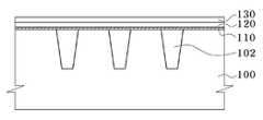
도 1 내지 도 3은 본 발명의 일 실시예에 따른 반도체 메모리소자의 게이트 형성방법을 설명하기 위한 단면도들로서, 전하트랩층을 갖는 불휘발성 메모리소자의 게이트 형성 과정을 나타내는 단면도들이다.1 to 3 are cross-sectional views illustrating a method of forming a gate of a semiconductor memory device according to an embodiment of the present invention, and are cross-sectional views illustrating a gate forming process of a nonvolatile memory device having a charge trap layer.
도 1을 참조하면, 소자분리막(102)이 형성된 반도체기판(100) 상에 터널링층(110)을 형성한다. 터널링층(110)은 습식산화(wet oxidation) 공정, 건식산화(dry oxidation) 공정 또는 라디컬산화(radical oxidation) 공정을 이용하여 옥사이드막으로 형성할 수 있다. 터널링층(110)을 형성한 후에는, NO 분위기 또는 N2O 분위기에서 열처리(anneal)를 수행하여 반도체기판(100)과 터널링층(110) 사이의 계면특성을 개선시킬 수 있다.Referring to FIG. 1, the
다음에 터널링층(110) 상에 전하트랩층(120)을 형성한다. 전하트랩층(120)은 스토이키오메트릭(sotichiometric) 실리콘나이트라이드(Si3N4)막, 실리콘-리치(Si-rich) 실리콘나이트라이드(SixNy)막, 또는 스토이키오메트릭 실리콘나이트라이드(Si3N4)막과 실리콘-리치(Si-rich) 실리콘나이트라이드(SixNy)막이 적층된 구조로 형성할 수 있다.Next, the
다음에, 전하트랩층(120) 상에, 전하트랩층(120)에 트랩된 전자가 컨트롤게 이트전극으로 빠져 나가는 것을 방지하기 위한 블로킹층(130)을 형성한다. 블로킹층(130)은 알루미늄옥사이드(Al2O3)막, 하프늄옥사이드(HfO2) 또는 하프늄알루미늄옥사이드(HfAlO)막과 같은 하이-케이(high-K) 물질을 포함하는 구조로 형성할 수 있다.Next, a blocking
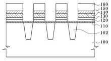
도 2를 참조하면, 블로킹층(130) 위에, 컨트롤게이트전극(140)과 저저항층(150)을 형성한다. 컨트롤게이트전극(140)은 예를 들어 n형 불순물이 고농도로 도핑된 폴리실리콘막으로 형성하거나, 일함수(work function)가 높은 금속, 예를 들어 텅스텐(W)막, 텅스텐실리사이드(WSi)막, 텅스텐나이트라이드(WN)막, 탄탈륨나이트라이드(TaN)막, 티타늄나이트라이드(TiN), 루테늄(Ru)막의 단일층 또는 이들의 적층막으로 형성할 수 있다. 저저항층(150)은 컨트롤게이트전극(140)의 저항을 낮추기 위한 것으로서, 폴리실리콘막/텅스텐실리사이드막 구조나, 또는 텅스텐나이트라이드(WN)막/텅스텐(W)막 구조로 형성한다.Referring to FIG. 2, the
저저항층(150) 위에, 게이트 패턴을 형성하기 위한 하드마스크(160)를 형성한다. 하드마스크(160)는 소정 두께의 실리콘질화막으로 형성한다. 다음, 상기 하드마스크(160)를 식각마스크로 사용하여 저저항층(150), 컨트롤게이트전극(140), 블로킹층(130), 전하트랩층(120) 및 터널링층(110)을 차례로 식각한다. 상기 식각공정은 높은 에너지의 플라즈마를 이용한 건식식각으로 이루어지는데, 이 과정에서 게이트 구조를 이루고 있는 막질들의 측면이 손상(damage)을 받게 되어 소자의 특성에 좋지 않은 영향을 미치게 된다. 특히 전하트랩층(120)의 측면에 발생한 손상 은 전하트랩층(120)에 트랩된 전하의 누설통로가 되어 소자의 정보저장 특성, 즉 리텐션 특성을 저하시키는 원인이 된다.A
이러한 게이트 패턴의 손상을 제거하기 위하여 통상적으로, 게이트 패터닝 후 세정공정을 진행하는데, 게이트 저항을 감소시키기 위하여 도입된 새로운 게이트 도전물질로 인해 세정공정에 많은 제한이 따르며 공정이 까다로워진다. 따라서, 게이트 측면 손상의 불충분한 제거로 인해 누설전류가 발생하여 제품의 신뢰성이 저하되는 결과가 초래될 수 있다. 본 발명에서는 식각공정으로 인한 게이트 패턴의 손상을 치유하기 위하여 다음과 같은 공정을 수행한다.In order to remove the damage of the gate pattern, the cleaning process is usually performed after the gate patterning, and the new gate conductive material introduced to reduce the gate resistance places many limitations on the cleaning process and makes the process difficult. Thus, insufficient removal of gate side damage can result in leakage currents resulting in a reduction in product reliability. In the present invention, the following process is performed to heal the damage of the gate pattern due to the etching process.
도 3을 참조하면, 이방성 건식식각으로 인해 게이트 패턴이 손상을 입은 상태에서 저온, 저압의 플라즈마 산화공정을 실시하여 게이트 패턴의 측면을 얇게 산화시켜 산화막(170)이 형성되도록 한다. 상기 저온, 저압 플라즈마 산화공정은 고밀도 플라즈마(HDP) 방식으로서 200 ∼ 500℃의 온도에서 산화반응이 일어나며, 공정 압력은 1 ∼ 100mT의 범위가 바람직하다. 상기 산화공정에서의 플라즈마를 형성하는 물질로는 산소(O2), 헬륨(He), 아르곤(Ar) 또는 수소(H2)를 하나 또는 둘 이상을 조합하여 사용할 수 있다. 상기 저온, 저압 플라즈마 산화공정에 의해 게이트 패턴 측면에 형성되는 산화막(170)의 두께는 게이트 패턴의 손상 정도 또는 게이트 도전층의 종류에 따라 달라질 수 있는데, 실리콘단결정을 기준으로 10 ∼ 100Å 정도가 형성되도록 하는 것이 바람직하다.Referring to FIG. 3, the
상기한 저온, 저압 플라즈마 산화공정에 의해 게이트 패턴 측면의 손상 부위 가 산화되면서 손상이 제거된다.The damage is removed while the damaged portion of the side of the gate pattern is oxidized by the low temperature and low pressure plasma oxidation process.
이상 본 발명을 바람직한 실시예를 들어 상세하게 설명하였으나, 본 발명은 상기 실시예에 한정되지 않으며, 본 발명의 기술적 사상 내에서 당 분야에서 통상의 지식을 가진 자에 의하여 여러 가지 변형이 가능함은 당연하다.Although the present invention has been described in detail with reference to preferred embodiments, the present invention is not limited to the above embodiments, and various modifications may be made by those skilled in the art within the technical spirit of the present invention. Do.
도 1 내지 도 3은 본 발명의 일 실시예에 전하트랩층을 갖는 불휘발성 메모리소자의 게이트 형성 과정을 나타내는 단면도들이다.1 to 3 are cross-sectional views illustrating a gate forming process of a nonvolatile memory device having a charge trap layer according to an embodiment of the present invention.
Claims (8)
Translated fromKoreanPriority Applications (3)
| Application Number | Priority Date | Filing Date | Title |
|---|---|---|---|
| KR1020070135871AKR20090068020A (en) | 2007-12-21 | 2007-12-21 | Gate forming method of a nonvolatile memory device having a charge trap layer |
| US12/131,558US20090163013A1 (en) | 2007-12-21 | 2008-06-02 | Method for Forming Gate of Non-Volatile Memory Device |
| CNA2008101469069ACN101465291A (en) | 2007-12-21 | 2008-08-26 | Method for forming gate of non-volatile memory device |
Applications Claiming Priority (1)
| Application Number | Priority Date | Filing Date | Title |
|---|---|---|---|
| KR1020070135871AKR20090068020A (en) | 2007-12-21 | 2007-12-21 | Gate forming method of a nonvolatile memory device having a charge trap layer |
Publications (1)
| Publication Number | Publication Date |
|---|---|
| KR20090068020Atrue KR20090068020A (en) | 2009-06-25 |
Family
ID=40789159
Family Applications (1)
| Application Number | Title | Priority Date | Filing Date |
|---|---|---|---|
| KR1020070135871ACeasedKR20090068020A (en) | 2007-12-21 | 2007-12-21 | Gate forming method of a nonvolatile memory device having a charge trap layer |
Country Status (3)
| Country | Link |
|---|---|
| US (1) | US20090163013A1 (en) |
| KR (1) | KR20090068020A (en) |
| CN (1) | CN101465291A (en) |
Families Citing this family (3)
| Publication number | Priority date | Publication date | Assignee | Title |
|---|---|---|---|---|
| US7755078B2 (en)* | 2008-06-13 | 2010-07-13 | Qucor Pty. Ltd. | Silicon single electron device |
| CN101807579A (en)* | 2010-03-16 | 2010-08-18 | 复旦大学 | Charge-captured non-volatilization semiconductor memory and manufacturing method thereof |
| CN113035882A (en)* | 2021-03-10 | 2021-06-25 | 山东大学 | Universal preparation method of non-volatile semiconductor memory |
Family Cites Families (7)
| Publication number | Priority date | Publication date | Assignee | Title |
|---|---|---|---|---|
| JP4727057B2 (en)* | 2001-03-28 | 2011-07-20 | 忠弘 大見 | Plasma processing equipment |
| KR100456596B1 (en)* | 2002-05-08 | 2004-11-09 | 삼성전자주식회사 | Method of erasing floating trap type non-volatile memory device |
| US6746925B1 (en)* | 2003-03-25 | 2004-06-08 | Lsi Logic Corporation | High-k dielectric bird's beak optimizations using in-situ O2 plasma oxidation |
| KR101133212B1 (en)* | 2005-01-05 | 2012-04-05 | 삼성전자주식회사 | Semiconductor devices having source/drain regions disposed at both sides of a channel region and methods of forming the same |
| KR100631278B1 (en)* | 2005-09-05 | 2006-10-04 | 동부일렉트로닉스 주식회사 | Nonvolatile Memory and Manufacturing Method Thereof |
| US7825018B2 (en)* | 2006-02-28 | 2010-11-02 | Tokyo Electron Limited | Plasma oxidation method and method for manufacturing semiconductor device |
| US7382650B2 (en)* | 2006-10-03 | 2008-06-03 | Spansion Llc | Method and apparatus for sector erase operation in a flash memory array |
- 2007
- 2007-12-21KRKR1020070135871Apatent/KR20090068020A/ennot_activeCeased
- 2008
- 2008-06-02USUS12/131,558patent/US20090163013A1/ennot_activeAbandoned
- 2008-08-26CNCNA2008101469069Apatent/CN101465291A/enactivePending
Also Published As
| Publication number | Publication date |
|---|---|
| CN101465291A (en) | 2009-06-24 |
| US20090163013A1 (en) | 2009-06-25 |
Similar Documents
| Publication | Publication Date | Title |
|---|---|---|
| CN101335208B (en) | Method of fabricating non-volatile memory device having charge trapping layer | |
| US7772637B2 (en) | Semiconductor devices including gate structures and leakage barrier oxides | |
| JP5361328B2 (en) | Method for manufacturing nonvolatile semiconductor memory device | |
| JP2005005715A (en) | SONOS memory device and manufacturing method thereof | |
| KR20090101592A (en) | Method of forming an oxide layer and method of forming a gate using the same | |
| US7692233B2 (en) | Semiconductor device and manufacturing method thereof | |
| CN101409309B (en) | Flash memory device and manufacturing method thereof | |
| US20150228739A1 (en) | Split gate embedded memory technology and manufacturing method thereof | |
| US20080001209A1 (en) | Non-volatile memory device and method of manufacturing the non-volatile memory device | |
| TWI555066B (en) | Semiconductor component manufacturing method | |
| US20080085584A1 (en) | Oxidation/heat treatment methods of manufacturing non-volatile memory devices | |
| US7897455B2 (en) | Semiconductor device and method of manufacturing the same | |
| KR100854875B1 (en) | Manufacturing Method of Flash Memory Device | |
| KR20090068020A (en) | Gate forming method of a nonvolatile memory device having a charge trap layer | |
| US20100093142A1 (en) | Method of fabricating device | |
| KR100759845B1 (en) | Nonvolatile Memory Device and Manufacturing Method Thereof | |
| US6696331B1 (en) | Method of protecting a stacked gate structure during fabrication | |
| KR20100108715A (en) | Method for manufacturing of non-volatile memory device | |
| KR20080060361A (en) | Method for manufacturing semiconductor device with MANOS structure | |
| KR100891423B1 (en) | Manufacturing Method of Flash Memory Device | |
| US7883963B2 (en) | Split charge storage node outer spacer process | |
| KR100771553B1 (en) | A buried nonvolatile memory device having a charge trap layer and a manufacturing method thereof | |
| KR100685626B1 (en) | Manufacturing Method of Flash Memory Device | |
| US20110133267A1 (en) | Method of fabricating semiconductor device and the semiconductor device | |
| KR20090036979A (en) | Method for manufacturing nonvolatile memory device having charge trap layer |
Legal Events
| Date | Code | Title | Description |
|---|---|---|---|
| A201 | Request for examination | ||
| PA0109 | Patent application | Patent event code:PA01091R01D Comment text:Patent Application Patent event date:20071221 | |
| PA0201 | Request for examination | ||
| PG1501 | Laying open of application | ||
| E902 | Notification of reason for refusal | ||
| PE0902 | Notice of grounds for rejection | Comment text:Notification of reason for refusal Patent event date:20090929 Patent event code:PE09021S01D | |
| E601 | Decision to refuse application | ||
| PE0601 | Decision on rejection of patent | Patent event date:20100226 Comment text:Decision to Refuse Application Patent event code:PE06012S01D Patent event date:20090929 Comment text:Notification of reason for refusal Patent event code:PE06011S01I |