KR20090065110A - LCD Display - Google Patents
LCD DisplayDownload PDFInfo
- Publication number
- KR20090065110A KR20090065110AKR1020070132554AKR20070132554AKR20090065110AKR 20090065110 AKR20090065110 AKR 20090065110AKR 1020070132554 AKR1020070132554 AKR 1020070132554AKR 20070132554 AKR20070132554 AKR 20070132554AKR 20090065110 AKR20090065110 AKR 20090065110A
- Authority
- KR
- South Korea
- Prior art keywords
- liquid crystal
- pixel
- pixels
- gate
- subpixel
- Prior art date
- Legal status (The legal status is an assumption and is not a legal conclusion. Google has not performed a legal analysis and makes no representation as to the accuracy of the status listed.)
- Withdrawn
Links
Images


Classifications
- G—PHYSICS
- G02—OPTICS
- G02F—OPTICAL DEVICES OR ARRANGEMENTS FOR THE CONTROL OF LIGHT BY MODIFICATION OF THE OPTICAL PROPERTIES OF THE MEDIA OF THE ELEMENTS INVOLVED THEREIN; NON-LINEAR OPTICS; FREQUENCY-CHANGING OF LIGHT; OPTICAL LOGIC ELEMENTS; OPTICAL ANALOGUE/DIGITAL CONVERTERS
- G02F1/00—Devices or arrangements for the control of the intensity, colour, phase, polarisation or direction of light arriving from an independent light source, e.g. switching, gating or modulating; Non-linear optics
- G02F1/01—Devices or arrangements for the control of the intensity, colour, phase, polarisation or direction of light arriving from an independent light source, e.g. switching, gating or modulating; Non-linear optics for the control of the intensity, phase, polarisation or colour
- G02F1/0121—Operation of devices; Circuit arrangements, not otherwise provided for in this subclass
- G02F1/0123—Circuits for the control or stabilisation of the bias voltage, e.g. automatic bias control [ABC] feedback loops
- G—PHYSICS
- G02—OPTICS
- G02F—OPTICAL DEVICES OR ARRANGEMENTS FOR THE CONTROL OF LIGHT BY MODIFICATION OF THE OPTICAL PROPERTIES OF THE MEDIA OF THE ELEMENTS INVOLVED THEREIN; NON-LINEAR OPTICS; FREQUENCY-CHANGING OF LIGHT; OPTICAL LOGIC ELEMENTS; OPTICAL ANALOGUE/DIGITAL CONVERTERS
- G02F1/00—Devices or arrangements for the control of the intensity, colour, phase, polarisation or direction of light arriving from an independent light source, e.g. switching, gating or modulating; Non-linear optics
- G02F1/01—Devices or arrangements for the control of the intensity, colour, phase, polarisation or direction of light arriving from an independent light source, e.g. switching, gating or modulating; Non-linear optics for the control of the intensity, phase, polarisation or colour
- G02F1/13—Devices or arrangements for the control of the intensity, colour, phase, polarisation or direction of light arriving from an independent light source, e.g. switching, gating or modulating; Non-linear optics for the control of the intensity, phase, polarisation or colour based on liquid crystals, e.g. single liquid crystal display cells
- G02F1/133—Constructional arrangements; Operation of liquid crystal cells; Circuit arrangements
- G02F1/1333—Constructional arrangements; Manufacturing methods
- G02F1/1335—Structural association of cells with optical devices, e.g. polarisers or reflectors
- G02F1/1336—Illuminating devices
- G02F1/133602—Direct backlight
- G02F1/133609—Direct backlight including means for improving the color mixing, e.g. white
- G—PHYSICS
- G09—EDUCATION; CRYPTOGRAPHY; DISPLAY; ADVERTISING; SEALS
- G09G—ARRANGEMENTS OR CIRCUITS FOR CONTROL OF INDICATING DEVICES USING STATIC MEANS TO PRESENT VARIABLE INFORMATION
- G09G3/00—Control arrangements or circuits, of interest only in connection with visual indicators other than cathode-ray tubes
- G09G3/20—Control arrangements or circuits, of interest only in connection with visual indicators other than cathode-ray tubes for presentation of an assembly of a number of characters, e.g. a page, by composing the assembly by combination of individual elements arranged in a matrix no fixed position being assigned to or needed to be assigned to the individual characters or partial characters
- G09G3/34—Control arrangements or circuits, of interest only in connection with visual indicators other than cathode-ray tubes for presentation of an assembly of a number of characters, e.g. a page, by composing the assembly by combination of individual elements arranged in a matrix no fixed position being assigned to or needed to be assigned to the individual characters or partial characters by control of light from an independent source
- G09G3/3406—Control of illumination source
- G09G3/3413—Details of control of colour illumination sources
- G—PHYSICS
- G02—OPTICS
- G02F—OPTICAL DEVICES OR ARRANGEMENTS FOR THE CONTROL OF LIGHT BY MODIFICATION OF THE OPTICAL PROPERTIES OF THE MEDIA OF THE ELEMENTS INVOLVED THEREIN; NON-LINEAR OPTICS; FREQUENCY-CHANGING OF LIGHT; OPTICAL LOGIC ELEMENTS; OPTICAL ANALOGUE/DIGITAL CONVERTERS
- G02F2201/00—Constructional arrangements not provided for in groups G02F1/00 - G02F7/00
- G02F2201/50—Protective arrangements
- G02F2201/506—Repairing, e.g. with redundant arrangement against defective part
- G02F2201/508—Pseudo repairing, e.g. a defective part is brought into a condition in which it does not disturb the functioning of the device
Landscapes
- Physics & Mathematics (AREA)
- Nonlinear Science (AREA)
- General Physics & Mathematics (AREA)
- Engineering & Computer Science (AREA)
- Optics & Photonics (AREA)
- Computer Hardware Design (AREA)
- Theoretical Computer Science (AREA)
- Mathematical Physics (AREA)
- Chemical & Material Sciences (AREA)
- Crystallography & Structural Chemistry (AREA)
- Control Of Indicators Other Than Cathode Ray Tubes (AREA)
- Liquid Crystal Display Device Control (AREA)
Abstract
Translated fromKoreanDescription
Translated fromKorean본 발명은 액정표시장치에서 액정패널의 픽셀 배열기술에 관한 것으로, 특히 액정패널상에 쿼드 타입의 픽셀을 배열할 때 크로스토크나 그리니쉬 또는 수직 딤(dim) 현상이 발생되는 것을 방지할 수 있도록 배열하는데 적당하도록 한 액정표시장치에 관한 것이다.BACKGROUND OF THE
최근, 정보기술(IT)의 발달에 따라 평판표시장치는 시각정보 전달매체로서 그 중요성이 한층 강조되고 있으며, 향후 보다 향상된 경쟁력을 확보하기 위해 저소비전력화, 박형화, 경량화, 고화질화 등이 요구되고 있다.Recently, with the development of information technology (IT), the importance of the flat panel display device as a visual information transmission medium has been further emphasized, and low power consumption, thinning, light weight, and high quality are required to secure improved competitiveness in the future.
평판표시장치의 대표적인 표시장치인 액정표시장치(LCD: Liquid Crystal Display)는 액정의 광학적 이방성을 이용하여 화상을 표시하는 장치로서, 박형, 소형, 저소비전력 및 고화질 등의 장점이 있다.A liquid crystal display (LCD), which is a typical display device of a flat panel display device, is an apparatus for displaying an image using optical anisotropy of liquid crystal, and has advantages such as thin, small size, low power consumption, and high quality.
이와 같은 액정 표시장치는 매트릭스(matrix) 형태로 배열된 화소들에 화상정보를 개별적으로 공급하여, 그 화소들의 광투과율을 조절함으로써, 원하는 화상을 표시할 수 있도록 한 표시장치이다. 따라서, 액정 표시장치는 화상을 구현하는 최소 단위인 화소들이 액티브 매트릭스 형태로 배열되는 액정 패널과, 상기 액정 패널을 구동하기 위한 구동부를 구비한다. 그리고, 상기 액정표시장치는 스스로 발광하지 못하기 때문에 액정표시장치에 광을 공급하는 백라이트 유닛이 구비된다. 상기 구동부는 타이밍 콘트롤러를 비롯하여 데이터 구동부와 게이트 구동부를 구비한다.Such a liquid crystal display device is a display device in which image information is individually supplied to pixels arranged in a matrix, and a desired image is displayed by adjusting light transmittance of the pixels. Accordingly, the liquid crystal display includes a liquid crystal panel in which pixels, which are the smallest unit for implementing an image, are arranged in an active matrix form, and a driving unit for driving the liquid crystal panel. Since the LCD does not emit light by itself, a backlight unit is provided to supply light to the LCD. The driver includes a timing controller and a data driver and a gate driver.
상기 액정패널의 구동방식에는 데이터라인에 인가되는 화소(또는 데이터)신호의 위상에 따라 라인 인버젼(line inversion), 컬럼 인버젼(column inversion), 및 도트 인버젼(dot inversion) 등의 방식이 있다. 상기 라인 인버젼 방식은 데이터라인에 인가되는 화소신호의 위상을 각 라인마다 반전시켜 인가하는 방식이고, 컬럼 인버젼 방식은 데이터라인에 인가되는 화소신호의 위상을 각 컬럼마다 반전시켜 인가하는 방식이고, 도트 인버젼 방식은 데이터라인에 인가되는 화소신호의 위상을 각 컬럼과 라인마다 반전시켜 인가하는 방식이다.The driving method of the liquid crystal panel includes a line inversion, column inversion, and dot inversion depending on the phase of the pixel (or data) signal applied to the data line. have. The line inversion method is a method of inverting and applying a phase of a pixel signal applied to a data line for each line, and the column inversion method is a method of inverting and applying a phase of a pixel signal applied to a data line for each column. The dot inversion method is a method of inverting and applying a phase of a pixel signal applied to a data line for each column and line.
상기와 같이, 인버젼 방식으로 액정을 구동하는 이유는 액정이 계속 한쪽 방향으로만 배열되어 열화현상이 나타나는 것을 방지하기 위함이다. 즉, 인버젼 방식이란 정극성의 영상신호와 부극성의 영상신호를 교대로 공급하여 액정이 한번은 오른쪽 방향으로 배열되고 다음에는 반대 방향으로 배열되도록 하기 위함이다.As described above, the reason for driving the liquid crystal in the inversion method is to prevent the deterioration phenomenon by the liquid crystal is continuously arranged in only one direction. In other words, the inversion method is to alternately supply a positive image signal and a negative image signal so that the liquid crystals are arranged in the right direction and then in the opposite direction.
최근 들어, 다양한 색상의 영상을 표현하기 위하여 액정패널에 기본적으로 사용하는 적,녹,청색(RGB)의 서브픽셀 이외에 어떠한 컬러성분도 없이 광량의 조절만 가능한 백색 서브픽셀(W)이 추가되어, 적,녹,청,백색(RGBW)의 4개의 서브픽셀로 하나의 픽셀을 이루는 쿼드 타입의 픽셀을 도입하여 화소 구조를 개선하고 이를 통해 휘도를 향상시키고자 하는 연구가 활발하게 진행되고 있다.Recently, in addition to the red, green and blue (RGB) subpixels that are basically used in the liquid crystal panel to express images of various colors, a white subpixel (W) that can only adjust the amount of light without any color component is added. In order to improve the pixel structure and to improve the luminance through the introduction of quad-type pixels forming one pixel with four subpixels of green, blue, and white (RGBW), research is being actively conducted.
도 1은 상기 쿼드 타입 픽셀의 배치도로서 RGBW 서브픽셀이 하나의 픽셀을 이루 는 쿼드(quad) 타입으로 배열된 것을 알 수 있다.FIG. 1 is a layout view of the quad type pixels, and it can be seen that RGBW subpixels are arranged in a quad type forming one pixel.
도 2의 (a)는 상기 RGBW 픽셀에 대한 종래의 픽셀 구조 중 1×N(수평×수직) 인버젼 구조를 나타낸 것으로, 이와 같은 구조에서는 인접된 픽셀간 서브픽셀들이 대응되는 극성으로 배열되어 있지 않아 공통전압(Vcom)이 정극성 또는 부극성 방향으로 시프트되는 현상이 발생되고, 이에 의해 공통전압(Vcom)이 불안정한 상태로 되며, 이에 따라 크로스토크(crosstalk), 그리니쉬(greenish) 현상 등이 발생되어 화질이 저하되었다.FIG. 2 (a) shows a 1 × N (horizontal × vertical) inversion structure of a conventional pixel structure for the RGBW pixel. In such a structure, subpixels between adjacent pixels are not arranged with corresponding polarities. As a result, a phenomenon in which the common voltage Vcom is shifted in the positive or negative polarity direction occurs, thereby causing the common voltage Vcom to become unstable, thereby causing crosstalk and greenish phenomenon. The image quality is reduced.
도 2의 (b)는 상기 RGBW 픽셀에 대한 종래의 픽셀 구조 중 2N×M(수평×수직) 인버젼 구조를 나타낸 것으로 이와 같은 구조에서는 상기와 같은 공통전압의 불안정한 상태는 발생되지 않지만, 픽셀을 기준으로 좌우 기생캐패시턴스(Cdp)의 영향차로 인하여 일정 간격으로 픽셀이 밝고,어두운 형태의 수직 딤(Dim) 문제가 발생되었으며, 특히 TN 모드의 모델에서 그 증상이 더욱 심각하게 나타났다.FIG. 2 (b) shows a 2N × M (horizontal × vertical) inversion structure of the conventional pixel structure for the RGBW pixel. In such a structure, the unstable state of the common voltage does not occur. As a reference, due to the difference between the left and right parasitic capacitances (Cdp), the pixels were bright at a certain interval, and a dark vertical dim problem occurred, especially in the TN mode model.
이와 같은 문제점을 해결하기 위해 제안된 종래의 픽셀 구조를 도 3에 나타내었다. 도 3의 픽셀구조를 살펴보면, 동일 극성을 가진 2개의 서브픽셀이 대각선 방향으로 배열됨과 아울러 나머지 2개의 서브픽셀이 역대각선 방향으로 각각 배열되고, 다음 픽셀에서는 그들의 극성이 서로 바뀌는 방식으로 배열된 것을 알 수 있다. 그러나, 도 3과 같은 픽셀 구조는 기존에 범용적으로 사용되고 있는 RGB 픽셀구조를 채용한 데이터구동 집적소자, 게이트구동 집적소자 등의 회로 부품을 공용화할 수 없는 결함이 있었다.The conventional pixel structure proposed to solve such a problem is shown in FIG. 3. Referring to the pixel structure of FIG. 3, two subpixels having the same polarity are arranged in a diagonal direction, and the remaining two subpixels are arranged in a reverse diagonal direction, respectively, and the next pixel is arranged in such a manner that their polarities are interchanged with each other. Able to know. However, the pixel structure shown in FIG. 3 has a defect in that circuit components such as a data driving integrated device and a gate driving integrated device employing the RGB pixel structure, which are conventionally used, cannot be shared.
이와 같이 종래 기술에 의한 액정표시장치의 액정패널에 있어서, 1×N 인버젼 구조의 액정패널에서는 공통전압이 불안정한 상태로 되어 크로스토크, 그리니쉬 현상 등이 발생되어 화질이 저하되는 문제점이 있었다.As described above, in the liquid crystal panel of the liquid crystal display device according to the prior art, the common voltage becomes unstable in the liquid crystal panel having a 1 × N inversion structure, resulting in crosstalk, greenish phenomenon, and the like, resulting in deterioration in image quality.
그리고, 2N×M 인버젼 구조의 액정패널에서는 픽셀을 기준으로 좌우 기생캐패시턴스의 영향차로 인하여 일정 간격으로 픽셀이 밝고,어두운 형태의 수직 딤(세로 선) 문제가 발생되었으며, TN 모드의 모델에서 그 증상이 더욱 심각하게 나타나는 문제점이 있었다.In the liquid crystal panel of 2N × M inversion structure, the pixels are bright at regular intervals due to the difference of left and right parasitic capacitance with respect to the pixels, and a dark vertical dim problem occurs in the TN mode model. There was a problem that the symptoms appeared more seriously.
그리고, 동일 극성의 서브픽셀이 대각선 역대각선 방향으로 배열된 구조를 가진 액정패널에서는 기존에 범용적으로 사용되고 있는 RGB 픽셀구조를 채용한 데이터구동 집적소자, 게이트구동 집적소자 등의 회로 부품을 공용화할 수 없는 문제점이 있었다.In addition, in a liquid crystal panel having a structure in which subpixels having the same polarity are arranged diagonally in diagonal directions, circuit components such as data driving integrated devices and gate driving integrated devices employing the RGB pixel structure, which are conventionally used in general, may be shared. There was a problem that could not be.
따라서, 본 발명의 목적은 도트 인버젼 방식으로 구동되는 액정패널상에 쿼드 타입의 픽셀을 배열할 때, 그들의 차징 전압이 서로 균형을 이루도록 배열하는데 있다.Accordingly, an object of the present invention is to arrange such that their charging voltages are balanced with each other when arranging quad type pixels on a liquid crystal panel driven by a dot inversion method.
상기와 같은 목적을 달성하기 위한 본 발명은, 도트 인버젼방식으로 구동되는 액정패널에 쿼드 타입의 픽셀을 배열할 때 수평방향으로 인접된 두 픽셀 간에 서브픽셀 RGBW가 경계면을 기준으로 대칭 구조를 이루도록 배열함을 특징으로 한다.In order to achieve the above object, the present invention provides a symmetrical structure of subpixel RGBW between two adjacent pixels in a horizontal direction when a quad type pixel is arranged in a liquid crystal panel driven by a dot inversion method. It is characterized by arrangement.
상기 액정패널의 구동방식은 수평1도트 수직2도트 인버젼 방식이나 수직1도트 수직1도트 인버젼 구동방식임을 특징으로 한다.The driving method of the liquid crystal panel is a horizontal 1 dot vertical 2 dot inversion method or a vertical 1 dot vertical 1 dot inversion driving method.
본 발명은 액정패널에 쿼드 타입의 픽셀을 배열할 때, 수평방향으로 인접된 두 픽셀의 서브픽셀 RGBW가 경계면을 기준으로 대칭 구조를 이루도록 배열함으로써, 도트 인버젼 방식을 적용할 때 정,부극성의 해당 서브픽셀들의 차징 전압이 서로 균형을 이루어 공통전압이 정극성이나 부극성 방향으로 시프트되지 않으므로 액정패널상의 각 서브픽셀들에 공통전압을 안정적으로 공급할 수 있는 효과가 있다.According to the present invention, when a pixel of a quad type is arranged in a liquid crystal panel, subpixel RGBWs of two pixels adjacent in a horizontal direction are arranged to form a symmetrical structure with respect to a boundary surface, thereby applying positive and negative polarities when applying the dot inversion method. Since the charging voltages of the corresponding subpixels are balanced with each other, the common voltage does not shift in the positive or negative direction, thereby stably supplying the common voltage to each subpixel on the liquid crystal panel.
그리고, 공통전압이 안정적으로 공급되어 크로스토크나 그리니쉬, 수직 딤(dim) 현상이 발생되는 것을 근본적으로 방지할 수 있는 효과가 있다.In addition, since the common voltage is stably supplied, there is an effect of fundamentally preventing crosstalk, greenish, and vertical dim from occurring.
이하, 첨부한 도면을 참조하여 본 발명의 바람직한 실시예를 상세히 설명하면 다음과 같다.Hereinafter, exemplary embodiments of the present invention will be described in detail with reference to the accompanying drawings.
도 4는 본 발명이 적용되는 액정표시장치의 블록도로서 이에 도시한 바와 같이, 게이트 구동부(2) 및 데이터 구동부(3)의 구동을 제어하기 위한 게이트 제어신호(GDC) 및 데이터 제어신호(DDC)를 출력함과 아울러, 디지털의 화소 데이터(RGB)를 샘플링한 후에 재정렬하여 출력하는 타이밍 콘트롤러(1)와; 상기 타이밍 콘트롤러(1)로부터 공급되는 게이트신호제어신호에 응답하여, 액정 패널(4)의 각 게이트라인(GL1∼GLn)에 게이트신호를 출력하는 게이트 구동부(2)와; 상기 타이밍 콘트롤러(1)로부터 공급되는 데이터신호제어신호에 응답하여 상기 액정 패널(4)의 각 데이터라인(DL1∼DLm)에 화소신호를 공급하는 데이터 구동부(3)와; 상기 게이트신호와 화소신호에 의해 구동되는 픽셀들을 매트릭스 형태로 구비하여 화상을 표시함에 있어서, 수평방향으로 인접된 두 픽셀의 쿼드타입의 서브픽셀 RGBW가 경계면을 기준으로 대칭 구조를 이루도록 배열된 액정패널(4)을 포함하여 구성한다.4 is a block diagram of a liquid crystal display device to which the present invention is applied. As shown in FIG. 4, the gate control signal GDC and the data control signal DDC for controlling the driving of the
도 5는 본 발명에 따른 상기 액정패널(4) 상의 쿼드타입 서브픽셀의 구조를 보인 것으로 이에 도시한 바와 같이, 수평방향으로 인접된 기수 픽셀과 우수 픽셀의 서브픽셀 RGBW가 경계면을 기준으로 서로 대칭적인 구조가 되도록 배열하였다.5 illustrates a structure of a quad type subpixel on the
이와 같이 구성한 본 발명의 작용을 첨부한 도 6을 참조하여 상세히 설명하면 다음과 같다.Referring to Figure 6 attached to the operation of the present invention configured as described above in detail as follows.
타이밍 콘트롤러(1)는 시스템으로부터 공급되는 수직/수평 동기신호(Hsync/Vsync)와 클럭신호(CLK)를 이용하여 게이트 구동부(2)를 제어하기 위한 게이트 제어신호(GDC)와 데이터 구동부(3)를 제어하기 위한 데이터 제어신호(DDC)를 출력한다. 이와 함께, 상기 타이밍 콘트롤러(1)는 상기 시스템으로부터 입력되는 디지털의 화소 데이터(RGB)를 샘플링한 후에 이를 재정렬하여 상기 데이터 구동부(3)에 공급한다.The
상기 게이트 제어신호(GDC)로서 게이트 스타트 펄스(GSP), 게이트 시프트 클럭(GSC), 게이트 아웃 인에이블(GOE) 등이 있고, 데이터 제어신호(DDC)로서 소스 스타트 펄스(SSP), 소스 시프트 클럭(SSC), 소스 아웃 인에이블(SOE), 극성신호(POL) 등이 있다.As the gate control signal GDC, there are a gate start pulse GSP, a gate shift clock GSC, a gate out enable GOE, and the like, and as a data control signal DDC, a source start pulse SSP and a source shift clock. (SSC), source out enable (SOE), polarity signal (POL), and the like.
게이트 구동부(2)는 상기 타이밍 콘트롤러(1)로부터 입력되는 게이트 제어신호(GDC)에 응답하여 게이트신호를 게이트라인(GL1∼GLn)에 순차적으로 공급하고, 이에 의해 수평라인 상의 해당 박막트랜지스터(TFT)들이 턴온된다. 이에 따라, 데이터라인(DL1∼DLm)을 통해 공급되는 화소신호들이 상기 박막트랜지스터(TFT)들을 통해 각각의 스토리지 캐패시터(CST)에 저장된다.The
이에 대해 좀 더 상세히 설명하면, 상기 게이트 구동부(2)는 상기 게이트 스타트 펄스(GSP)를 게이트 시프트 클럭(GSC)에 따라 시프트시켜 시프트 펄스를 발생한다. 그리고, 게이트 구동부(2)는 상기 시프트 클럭에 응답하여 수평기간마다 해당 게이트라인(GL)에 게이트 온,오프구간(신호)으로 이루어진 게이트신호를 공급하게 된다. 이 경우 상기 게이트 구동부(2)는 상기 게이트 아웃 인에이블신호(GOE)에 응답하여 인에이블 기간에서만 게이트 온 신호를 공급하고, 그 외의 기간에서는 게이 트 오프 신호(게이트 로우 신호)를 공급하게 된다.In more detail, the
데이터 구동부(3)는 상기 타이밍 콘트롤러(1)로부터 입력되는 데이터 제어신호(DDC)에 응답하여 상기 화소 데이터(RGB)를 계조값에 대응하는 아날로그의 화소신호(데이터신호 또는 데이터전압)로 변환하고, 이렇게 변환된 화소신호를 액정패널(4)상의 데이터라인(DL1∼DLm)에 공급한다.The
이에 대해 좀 더 상세히 설명하면, 상기 데이터 구동부(3)는 상기 소스 스타트 펄스(SSP)를 소스 시프트 클럭에 따라 시프트시켜 샘플링신호를 발생한다. 이어서, 상기 데이터 구동부(3)는 상기 샘플링신호에 응답하여 상기 화소 데이터(RGB)를 일정 단위씩 순차적으로 입력하여 래치한다. 그리고, 상기 데이터 구동부(3)는 래치된 1 라인분의 화소데이터(RGB)를 아날로그의 화소신호로 변환하여 데이터라인(DL1∼DLm)에 공급하게 된다.In more detail, the
액정패널(4)은 매트릭스 형태로 배열된 다수의 액정셀(CLC)들과, 데이터라인(DL1∼DLm)과 게이트라인(GL1∼GLn)의 교차부마다 형성되어 상기 각 액정셀(CLC)들 각각에 접속된 박막 트랜지스터(TFT)를 구비한다.The
상기 박막 트랜지스터(TFT)는 게이트라인(GL)으로부터 게이트신호가 공급되는 경우 턴온되어 상기 데이터라인(DL)을 통해 공급되는 화소신호를 액정셀(CLC)에 공급한다. 그리고, 상기 박막 트랜지스터(TFT)는 상기 게이트라인(GL)을 통해 게이트 오프 신호가 공급될 때 턴오프되어 액정셀(CLC)에 충전된 화소 신호가 유지되게 한다.The thin film transistor TFT is turned on when the gate signal is supplied from the gate line GL, and supplies the pixel signal supplied through the data line DL to the liquid crystal cell CLC . The thin film transistor TFT is turned off when the gate off signal is supplied through the gate line GL to maintain the pixel signal charged in the liquid crystal cell CLC .
상기 액정셀(CLC)은 액정을 사이에 두고 공통전극과 박막 트랜지스터(TFT)에 접속된 화소전극을 포함한다. 그리고, 상기 액정셀(CLC)은 충전된 화소 신호가 다음 화소 신호가 충전될 때까지 안정적으로 유지되게 하기 위하여 스토리지 캐패시터(CST)를 더 구비한다. 상기 스토리지 캐패시터(CST)는 화소 전극과 이전단 게이트라인의 사이에 형성된다. 이러한 액정셀(CLC)은 상기 박막 트랜지스터(TFT)를 통해 충전되는 화소 신호에 따라 유전 이방성을 가지는 액정의 배열 상태가 가변되고, 이에 따라 광투과율이 조절되어 계조가 구현된다.The liquid crystal cell CLC includes a pixel electrode connected to a common electrode and a thin film transistor TFT with a liquid crystal interposed therebetween. The liquid crystal cell CLC further includes a storage capacitor CST so that the charged pixel signal is stably maintained until the next pixel signal is charged. The storage capacitor CST is formed between the pixel electrode and the previous gate line. In the liquid crystal cell CLC , an arrangement state of liquid crystals having dielectric anisotropy varies according to pixel signals charged through the thin film transistor TFT, and light transmittance is adjusted accordingly to implement gradation.
한편, 본 발명에서는 상기 액정패널(4)상에 쿼드 타입의 픽셀을 배열함에 있어서, 임의의 한 픽셀의 서브픽셀 RGBW는 수평방향으로 인접한 픽셀의 서브픽셀 RGBW와 대칭 구조를 이루도록 하여 공통전압이 안정화된 상태를 유지할 수 있도록 하였는데, 이에 대하여 좀 더 상세히 설명하면 다음과 같다.Meanwhile, in the present invention, in arranging the quad type pixels on the
도 5는 상기 액정패널(4)상에서 본 발명에 따른 픽셀 구조를 나타낸 것으로, 적,녹,청,백색(RGBW)의 4개의 서브픽셀이 하나의 픽셀을 이루는 쿼드(quad) 타입의 픽셀 구조에서, 한 픽셀의 서브픽셀 RGBW는 수평방향으로 인접한 픽셀의 서브픽셀 RGBW와 대칭 구조를 이룬 것을 알 수 있다.FIG. 5 illustrates a pixel structure according to the present invention on the
즉, 수평방향으로 인접된 기수,우수 픽셀의 경계면을 기준으로 할 때, 기수 픽셀에서는 2사분면을 기준으로 시계 방향으로 RGBW 서브픽셀을 순차적으로 배열하고, 우수픽셀에서는 2사분면을 기준으로 시계 방향으로 GRWB 서브픽셀을 순차적으로 배열하였다.In other words, when the horizontal and the adjacent boundary of the odd and excellent pixels are referred to, the odd pixels sequentially arrange the RGBW subpixels in the clockwise direction with respect to the two quadrants, and in the even pixel, in the clockwise direction with respect to the two quadrants. GRWB subpixels were arranged sequentially.
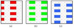
도 6은 상기 도 5에서와 같은 픽셀 구조를 수평 1도트 수직 2도트 인버젼에 적용한 예를 나타낸 것으로, 이와 같은 경우 수평 방향으로 인접된 픽셀 간에 서로 다른 극성을 가지는 동일 색상의 서브픽셀들이 인접되게 배열된 것을 알 수 있다.FIG. 6 illustrates an example in which the pixel structure as shown in FIG. 5 is applied to a horizontal 1-dot vertical 2-dot inversion. In such a case, subpixels having the same polarity having different polarities are adjacent to adjacent pixels in the horizontal direction. You can see that it is arranged.
즉, 첫 번째 수평라인의 픽셀들을 예로 할 때, 도 6의 (a)에서와 같이 두 번째 픽셀의 부극성의 R 서브픽셀과 세 번째 픽셀의 정극성의 R 서브픽셀을 서로 인접되게 배열한다.That is, when the pixels of the first horizontal line are taken as an example, as shown in FIG. 6A, the negative R subpixels of the second pixel and the positive R subpixels of the third pixel are arranged adjacent to each other.
도 6의 (b)에서와 같이 첫 번째 픽셀의 부극성의 G 서브픽셀과 두 번째 픽셀의 정극성의 G 서브픽셀을 인접되게 배열한다. 이와 마찬가지로, 세 번째 픽셀의 부극성의 G 서브픽셀과 네 번째 픽셀의 정극성의 G 서브픽셀을 인접되게 배열한다.As shown in FIG. 6B, the negative G subpixel of the first pixel and the positive G subpixel of the second pixel are arranged adjacent to each other. Similarly, the negative G subpixel of the third pixel and the positive G subpixel of the fourth pixel are arranged adjacently.
도 6의 (c)에서와 같이 첫 번째 픽셀의 부극성의 B 서브픽셀과 두 번째 픽셀의 정극성의 B 서브픽셀을 인접되게 배열한다. 이와 마찬가지로, 세 번째 픽셀의 부극성의 B 서브픽셀과 네 번째 픽셀의 정극성의 B 서브픽셀을 인접되게 배열한다.As shown in FIG. 6C, the negative B subpixel of the first pixel and the positive B subpixel of the second pixel are arranged adjacent to each other. Similarly, the negative B subpixel of the third pixel and the positive B subpixel of the fourth pixel are arranged adjacently.
이렇게 함으로써, 정,부극성의 해당 서브픽셀들의 차징 전압이 서로 균형을 이루어 공통전압이 정극성이나 부극성 방향으로 시프트되는 일이 발생되지 않는다. 이에 따라, 액정패널(4)상의 각 서브픽셀들에 공통전압을 안정적으로 공급할 수 있게 된다.In this way, the charging voltages of the corresponding subpixels of the positive and negative polarities are balanced with each other so that the common voltage is not shifted in the positive or negative direction. Accordingly, the common voltage can be stably supplied to each subpixel on the
한편, 도 7은 상기 도 5에서와 같은 본 발명의 픽셀 구조를 수평 1도트 수직 1도트 인버젼에 적용한 예를 나타낸 것이며, 여기에서는 B 서브픽셀을 예시적으로 나타낸 것이다. 이와 같은 경우에도 상기 설명에서와 같이 수평 방향으로 인접된 픽셀 간에 서로 다른 극성을 가지는 B 서브픽셀이 인접되게 배열된 것을 알 수 있 다.FIG. 7 illustrates an example in which the pixel structure of the present invention as shown in FIG. 5 is applied to a horizontal 1 dot vertical 1 dot inversion, and B subpixel is exemplarily shown. Even in such a case, it can be seen that B subpixels having different polarities are arranged adjacent to each other in the horizontal direction as in the above description.
따라서, 정,부극성의 해당 서브픽셀들의 차징 전압이 서로 균형을 이루어 공통전압이 정극성이나 부극성 방향으로 시프트되는 일이 발생되지 않는다. 이에 따라, 액정패널(4)상의 각 서브픽셀들에 공통전압을 안정적으로 공급할 수 있게 된다.Therefore, the charging voltages of the corresponding subpixels of the positive and negative polarities are balanced with each other so that the common voltage is not shifted in the positive or negative direction. Accordingly, the common voltage can be stably supplied to each subpixel on the
도 1은 쿼드 타입 픽셀의 배치도.1 is a layout view of quad type pixels.
도 2의 (a)는 수평1도트 수직2도트 인버젼 방식의 픽셀 배치도이고,2 (a) is a pixel arrangement diagram of a horizontal 1 dot vertical 2 dot inversion method,
도 2의 (b)는 수평2도트 수직2도트 인버젼 방식의 픽셀 배치도.Figure 2 (b) is a pixel arrangement diagram of a horizontal 2-dot vertical 2-dot inversion method.
도 3은 종래 기술에 의한 수평2도트 수직1도트 인버젼 방식의 픽셀 배치도.3 is a pixel arrangement diagram of a horizontal 2-dot vertical 1-dot inversion scheme according to the prior art;
도 4는 본 발명이 적용되는 액정표시장치의 구동 블록도.4 is a driving block diagram of a liquid crystal display device to which the present invention is applied.
도 5는 본 발명에 의한 액정패널의 픽셀 배치도.5 is a pixel layout view of a liquid crystal panel according to the present invention;
도 6의 (a)-(c)는 RGB 서브픽셀별 대칭 구조를 보인 설명도.6 (a) to 6 (c) are explanatory diagrams showing a symmetrical structure for each RGB subpixel.
도 7은 본 발명의 다른 실시예를보인 수평1도트 수직1도트 인버젼 방식의 픽셀 배치도.FIG. 7 is a pixel layout view of a horizontal 1 dot vertical 1 dot inversion scheme according to another embodiment of the present invention. FIG.
***도면의 주요 부분에 대한 부호의 설명****** Description of the symbols for the main parts of the drawings ***
1 : 타이밍 콘트롤러2 : 게이트 구동부1: Timing Controller 2: Gate Driver
3 : 데이터 구동부4 : 액정패널3: data driver 4: liquid crystal panel
Claims (5)
Translated fromKoreanPriority Applications (1)
| Application Number | Priority Date | Filing Date | Title |
|---|---|---|---|
| KR1020070132554AKR20090065110A (en) | 2007-12-17 | 2007-12-17 | LCD Display |
Applications Claiming Priority (1)
| Application Number | Priority Date | Filing Date | Title |
|---|---|---|---|
| KR1020070132554AKR20090065110A (en) | 2007-12-17 | 2007-12-17 | LCD Display |
Publications (1)
| Publication Number | Publication Date |
|---|---|
| KR20090065110Atrue KR20090065110A (en) | 2009-06-22 |
Family
ID=40993555
Family Applications (1)
| Application Number | Title | Priority Date | Filing Date |
|---|---|---|---|
| KR1020070132554AWithdrawnKR20090065110A (en) | 2007-12-17 | 2007-12-17 | LCD Display |
Country Status (1)
| Country | Link |
|---|---|
| KR (1) | KR20090065110A (en) |
Cited By (6)
| Publication number | Priority date | Publication date | Assignee | Title |
|---|---|---|---|---|
| CN103163680A (en)* | 2011-12-08 | 2013-06-19 | 东莞万士达液晶显示器有限公司 | Color filter substrate and liquid crystal display panel |
| KR20140013452A (en)* | 2012-07-24 | 2014-02-05 | 삼성디스플레이 주식회사 | Display panel and display apparatus having the same |
| KR20150077181A (en)* | 2013-12-27 | 2015-07-07 | 엘지디스플레이 주식회사 | Liquid crystal display |
| WO2016062049A1 (en)* | 2014-10-20 | 2016-04-28 | 京东方科技集团股份有限公司 | Pixel structure, display substrate and display device |
| US9335853B2 (en) | 2011-08-16 | 2016-05-10 | Samsung Display Co., Ltd. | Display device including sensor units and driving method thereof |
| US9715861B2 (en) | 2013-02-18 | 2017-07-25 | Samsung Display Co., Ltd | Display device having unit pixel defined by even number of adjacent sub-pixels |
- 2007
- 2007-12-17KRKR1020070132554Apatent/KR20090065110A/ennot_activeWithdrawn
Cited By (7)
| Publication number | Priority date | Publication date | Assignee | Title |
|---|---|---|---|---|
| US9335853B2 (en) | 2011-08-16 | 2016-05-10 | Samsung Display Co., Ltd. | Display device including sensor units and driving method thereof |
| CN103163680A (en)* | 2011-12-08 | 2013-06-19 | 东莞万士达液晶显示器有限公司 | Color filter substrate and liquid crystal display panel |
| KR20140013452A (en)* | 2012-07-24 | 2014-02-05 | 삼성디스플레이 주식회사 | Display panel and display apparatus having the same |
| US9715861B2 (en) | 2013-02-18 | 2017-07-25 | Samsung Display Co., Ltd | Display device having unit pixel defined by even number of adjacent sub-pixels |
| KR20150077181A (en)* | 2013-12-27 | 2015-07-07 | 엘지디스플레이 주식회사 | Liquid crystal display |
| WO2016062049A1 (en)* | 2014-10-20 | 2016-04-28 | 京东方科技集团股份有限公司 | Pixel structure, display substrate and display device |
| US10032401B2 (en) | 2014-10-20 | 2018-07-24 | Boe Technology Group Co., Ltd. | Pixel structure, display substrate and display apparatus |
Similar Documents
| Publication | Publication Date | Title |
|---|---|---|
| US8970564B2 (en) | Apparatus and method for driving liquid crystal display | |
| US8384708B2 (en) | Apparatus and method for dividing liquid crystal display device | |
| KR101127593B1 (en) | Liquid crystal display device | |
| US9548031B2 (en) | Display device capable of driving at low speed | |
| KR101264721B1 (en) | liquid crystal display apparatus | |
| KR101904013B1 (en) | Liquid crystal display device | |
| KR100475167B1 (en) | Liquid crystal display and method of driving the same | |
| KR20070059340A (en) | Liquid crystal display | |
| KR101415064B1 (en) | Device and method for driving a liquid crystal display device | |
| KR20110107581A (en) | Display device and driving method thereof | |
| CN105652540A (en) | Display panel | |
| US8717271B2 (en) | Liquid crystal display having an inverse polarity between a common voltage and a data signal | |
| KR20110070178A (en) | Driving device of liquid crystal display and driving method thereof | |
| KR20090065110A (en) | LCD Display | |
| KR102134320B1 (en) | Liquid crystal display | |
| KR101985245B1 (en) | Liquid crystal display | |
| KR20120090888A (en) | Liquid crystal display | |
| KR102009441B1 (en) | Liquid crystal display | |
| KR20170071219A (en) | Liquid crystal display device | |
| KR100931488B1 (en) | Liquid crystal display panel | |
| KR20080026278A (en) | Data driving device and driving method thereof | |
| KR102244985B1 (en) | Display panel | |
| KR101376655B1 (en) | Common voltage supply circuit of liquid crystal display device | |
| KR101470624B1 (en) | Liquid Crystal Display | |
| KR100928929B1 (en) | Inversion driving device and method of liquid crystal display device |
Legal Events
| Date | Code | Title | Description |
|---|---|---|---|
| PA0109 | Patent application | Patent event code:PA01091R01D Comment text:Patent Application Patent event date:20071217 | |
| PG1501 | Laying open of application | ||
| PC1203 | Withdrawal of no request for examination | ||
| WITN | Application deemed withdrawn, e.g. because no request for examination was filed or no examination fee was paid |