KR20090063207A - Compensation method for organic light emitting diode luminance deterioration - Google Patents
Compensation method for organic light emitting diode luminance deteriorationDownload PDFInfo
- Publication number
- KR20090063207A KR20090063207AKR1020097002992AKR20097002992AKR20090063207AKR 20090063207 AKR20090063207 AKR 20090063207AKR 1020097002992 AKR1020097002992 AKR 1020097002992AKR 20097002992 AKR20097002992 AKR 20097002992AKR 20090063207 AKR20090063207 AKR 20090063207A
- Authority
- KR
- South Korea
- Prior art keywords
- pixel
- capacitance
- current
- display
- readout
- Prior art date
- Legal status (The legal status is an assumption and is not a legal conclusion. Google has not performed a legal analysis and makes no representation as to the accuracy of the status listed.)
- Withdrawn
Links
- 238000000034methodMethods0.000titleclaimsabstractdescription34
- 230000006866deteriorationEffects0.000titleclaimsdescription13
- 238000012937correctionMethods0.000claimsabstractdescription49
- 230000015556catabolic processEffects0.000claimsabstractdescription10
- 238000006731degradation reactionMethods0.000claimsabstractdescription10
- 239000003990capacitorSubstances0.000claimsdescription22
- 230000003071parasitic effectEffects0.000claimsdescription20
- 230000032683agingEffects0.000abstractdescription19
- 230000002596correlated effectEffects0.000abstractdescription2
- 238000005259measurementMethods0.000description9
- 238000010586diagramMethods0.000description8
- 239000011368organic materialSubstances0.000description5
- 230000001276controlling effectEffects0.000description4
- 230000007423decreaseEffects0.000description2
- 239000012780transparent materialSubstances0.000description2
- 239000003086colorantSubstances0.000description1
- 238000013461designMethods0.000description1
- 238000013213extrapolationMethods0.000description1
- 230000005525hole transportEffects0.000description1
- AMGQUBHHOARCQH-UHFFFAOYSA-Nindium;oxotinChemical compound[In].[Sn]=OAMGQUBHHOARCQH-UHFFFAOYSA-N0.000description1
- 238000012986modificationMethods0.000description1
- 230000004048modificationEffects0.000description1
- 238000012797qualificationMethods0.000description1
- 238000003530single readoutMethods0.000description1
- 239000000758substrateSubstances0.000description1
Images


Classifications
- G—PHYSICS
- G09—EDUCATION; CRYPTOGRAPHY; DISPLAY; ADVERTISING; SEALS
- G09G—ARRANGEMENTS OR CIRCUITS FOR CONTROL OF INDICATING DEVICES USING STATIC MEANS TO PRESENT VARIABLE INFORMATION
- G09G3/00—Control arrangements or circuits, of interest only in connection with visual indicators other than cathode-ray tubes
- G09G3/20—Control arrangements or circuits, of interest only in connection with visual indicators other than cathode-ray tubes for presentation of an assembly of a number of characters, e.g. a page, by composing the assembly by combination of individual elements arranged in a matrix no fixed position being assigned to or needed to be assigned to the individual characters or partial characters
- G09G3/22—Control arrangements or circuits, of interest only in connection with visual indicators other than cathode-ray tubes for presentation of an assembly of a number of characters, e.g. a page, by composing the assembly by combination of individual elements arranged in a matrix no fixed position being assigned to or needed to be assigned to the individual characters or partial characters using controlled light sources
- G09G3/30—Control arrangements or circuits, of interest only in connection with visual indicators other than cathode-ray tubes for presentation of an assembly of a number of characters, e.g. a page, by composing the assembly by combination of individual elements arranged in a matrix no fixed position being assigned to or needed to be assigned to the individual characters or partial characters using controlled light sources using electroluminescent panels
- G09G3/32—Control arrangements or circuits, of interest only in connection with visual indicators other than cathode-ray tubes for presentation of an assembly of a number of characters, e.g. a page, by composing the assembly by combination of individual elements arranged in a matrix no fixed position being assigned to or needed to be assigned to the individual characters or partial characters using controlled light sources using electroluminescent panels semiconductive, e.g. using light-emitting diodes [LED]
- G09G3/3208—Control arrangements or circuits, of interest only in connection with visual indicators other than cathode-ray tubes for presentation of an assembly of a number of characters, e.g. a page, by composing the assembly by combination of individual elements arranged in a matrix no fixed position being assigned to or needed to be assigned to the individual characters or partial characters using controlled light sources using electroluminescent panels semiconductive, e.g. using light-emitting diodes [LED] organic, e.g. using organic light-emitting diodes [OLED]
- G09G3/3225—Control arrangements or circuits, of interest only in connection with visual indicators other than cathode-ray tubes for presentation of an assembly of a number of characters, e.g. a page, by composing the assembly by combination of individual elements arranged in a matrix no fixed position being assigned to or needed to be assigned to the individual characters or partial characters using controlled light sources using electroluminescent panels semiconductive, e.g. using light-emitting diodes [LED] organic, e.g. using organic light-emitting diodes [OLED] using an active matrix
- G09G3/3233—Control arrangements or circuits, of interest only in connection with visual indicators other than cathode-ray tubes for presentation of an assembly of a number of characters, e.g. a page, by composing the assembly by combination of individual elements arranged in a matrix no fixed position being assigned to or needed to be assigned to the individual characters or partial characters using controlled light sources using electroluminescent panels semiconductive, e.g. using light-emitting diodes [LED] organic, e.g. using organic light-emitting diodes [OLED] using an active matrix with pixel circuitry controlling the current through the light-emitting element
- G—PHYSICS
- G09—EDUCATION; CRYPTOGRAPHY; DISPLAY; ADVERTISING; SEALS
- G09G—ARRANGEMENTS OR CIRCUITS FOR CONTROL OF INDICATING DEVICES USING STATIC MEANS TO PRESENT VARIABLE INFORMATION
- G09G3/00—Control arrangements or circuits, of interest only in connection with visual indicators other than cathode-ray tubes
- G09G3/20—Control arrangements or circuits, of interest only in connection with visual indicators other than cathode-ray tubes for presentation of an assembly of a number of characters, e.g. a page, by composing the assembly by combination of individual elements arranged in a matrix no fixed position being assigned to or needed to be assigned to the individual characters or partial characters
- G09G3/22—Control arrangements or circuits, of interest only in connection with visual indicators other than cathode-ray tubes for presentation of an assembly of a number of characters, e.g. a page, by composing the assembly by combination of individual elements arranged in a matrix no fixed position being assigned to or needed to be assigned to the individual characters or partial characters using controlled light sources
- G09G3/30—Control arrangements or circuits, of interest only in connection with visual indicators other than cathode-ray tubes for presentation of an assembly of a number of characters, e.g. a page, by composing the assembly by combination of individual elements arranged in a matrix no fixed position being assigned to or needed to be assigned to the individual characters or partial characters using controlled light sources using electroluminescent panels
- G—PHYSICS
- G09—EDUCATION; CRYPTOGRAPHY; DISPLAY; ADVERTISING; SEALS
- G09G—ARRANGEMENTS OR CIRCUITS FOR CONTROL OF INDICATING DEVICES USING STATIC MEANS TO PRESENT VARIABLE INFORMATION
- G09G3/00—Control arrangements or circuits, of interest only in connection with visual indicators other than cathode-ray tubes
- G09G3/20—Control arrangements or circuits, of interest only in connection with visual indicators other than cathode-ray tubes for presentation of an assembly of a number of characters, e.g. a page, by composing the assembly by combination of individual elements arranged in a matrix no fixed position being assigned to or needed to be assigned to the individual characters or partial characters
- G09G3/22—Control arrangements or circuits, of interest only in connection with visual indicators other than cathode-ray tubes for presentation of an assembly of a number of characters, e.g. a page, by composing the assembly by combination of individual elements arranged in a matrix no fixed position being assigned to or needed to be assigned to the individual characters or partial characters using controlled light sources
- G09G3/30—Control arrangements or circuits, of interest only in connection with visual indicators other than cathode-ray tubes for presentation of an assembly of a number of characters, e.g. a page, by composing the assembly by combination of individual elements arranged in a matrix no fixed position being assigned to or needed to be assigned to the individual characters or partial characters using controlled light sources using electroluminescent panels
- G09G3/32—Control arrangements or circuits, of interest only in connection with visual indicators other than cathode-ray tubes for presentation of an assembly of a number of characters, e.g. a page, by composing the assembly by combination of individual elements arranged in a matrix no fixed position being assigned to or needed to be assigned to the individual characters or partial characters using controlled light sources using electroluminescent panels semiconductive, e.g. using light-emitting diodes [LED]
- G09G3/3208—Control arrangements or circuits, of interest only in connection with visual indicators other than cathode-ray tubes for presentation of an assembly of a number of characters, e.g. a page, by composing the assembly by combination of individual elements arranged in a matrix no fixed position being assigned to or needed to be assigned to the individual characters or partial characters using controlled light sources using electroluminescent panels semiconductive, e.g. using light-emitting diodes [LED] organic, e.g. using organic light-emitting diodes [OLED]
- G09G3/3225—Control arrangements or circuits, of interest only in connection with visual indicators other than cathode-ray tubes for presentation of an assembly of a number of characters, e.g. a page, by composing the assembly by combination of individual elements arranged in a matrix no fixed position being assigned to or needed to be assigned to the individual characters or partial characters using controlled light sources using electroluminescent panels semiconductive, e.g. using light-emitting diodes [LED] organic, e.g. using organic light-emitting diodes [OLED] using an active matrix
- G09G3/3233—Control arrangements or circuits, of interest only in connection with visual indicators other than cathode-ray tubes for presentation of an assembly of a number of characters, e.g. a page, by composing the assembly by combination of individual elements arranged in a matrix no fixed position being assigned to or needed to be assigned to the individual characters or partial characters using controlled light sources using electroluminescent panels semiconductive, e.g. using light-emitting diodes [LED] organic, e.g. using organic light-emitting diodes [OLED] using an active matrix with pixel circuitry controlling the current through the light-emitting element
- G09G3/3241—Control arrangements or circuits, of interest only in connection with visual indicators other than cathode-ray tubes for presentation of an assembly of a number of characters, e.g. a page, by composing the assembly by combination of individual elements arranged in a matrix no fixed position being assigned to or needed to be assigned to the individual characters or partial characters using controlled light sources using electroluminescent panels semiconductive, e.g. using light-emitting diodes [LED] organic, e.g. using organic light-emitting diodes [OLED] using an active matrix with pixel circuitry controlling the current through the light-emitting element the current through the light-emitting element being set using a data current provided by the data driver, e.g. by using a two-transistor current mirror
- G—PHYSICS
- G09—EDUCATION; CRYPTOGRAPHY; DISPLAY; ADVERTISING; SEALS
- G09G—ARRANGEMENTS OR CIRCUITS FOR CONTROL OF INDICATING DEVICES USING STATIC MEANS TO PRESENT VARIABLE INFORMATION
- G09G3/00—Control arrangements or circuits, of interest only in connection with visual indicators other than cathode-ray tubes
- G09G3/20—Control arrangements or circuits, of interest only in connection with visual indicators other than cathode-ray tubes for presentation of an assembly of a number of characters, e.g. a page, by composing the assembly by combination of individual elements arranged in a matrix no fixed position being assigned to or needed to be assigned to the individual characters or partial characters
- G09G3/22—Control arrangements or circuits, of interest only in connection with visual indicators other than cathode-ray tubes for presentation of an assembly of a number of characters, e.g. a page, by composing the assembly by combination of individual elements arranged in a matrix no fixed position being assigned to or needed to be assigned to the individual characters or partial characters using controlled light sources
- G09G3/30—Control arrangements or circuits, of interest only in connection with visual indicators other than cathode-ray tubes for presentation of an assembly of a number of characters, e.g. a page, by composing the assembly by combination of individual elements arranged in a matrix no fixed position being assigned to or needed to be assigned to the individual characters or partial characters using controlled light sources using electroluminescent panels
- G09G3/32—Control arrangements or circuits, of interest only in connection with visual indicators other than cathode-ray tubes for presentation of an assembly of a number of characters, e.g. a page, by composing the assembly by combination of individual elements arranged in a matrix no fixed position being assigned to or needed to be assigned to the individual characters or partial characters using controlled light sources using electroluminescent panels semiconductive, e.g. using light-emitting diodes [LED]
- G09G3/3208—Control arrangements or circuits, of interest only in connection with visual indicators other than cathode-ray tubes for presentation of an assembly of a number of characters, e.g. a page, by composing the assembly by combination of individual elements arranged in a matrix no fixed position being assigned to or needed to be assigned to the individual characters or partial characters using controlled light sources using electroluminescent panels semiconductive, e.g. using light-emitting diodes [LED] organic, e.g. using organic light-emitting diodes [OLED]
- G09G3/3275—Details of drivers for data electrodes
- G09G3/3283—Details of drivers for data electrodes in which the data driver supplies a variable data current for setting the current through, or the voltage across, the light-emitting elements
- H—ELECTRICITY
- H05—ELECTRIC TECHNIQUES NOT OTHERWISE PROVIDED FOR
- H05B—ELECTRIC HEATING; ELECTRIC LIGHT SOURCES NOT OTHERWISE PROVIDED FOR; CIRCUIT ARRANGEMENTS FOR ELECTRIC LIGHT SOURCES, IN GENERAL
- H05B45/00—Circuit arrangements for operating light-emitting diodes [LED]
- H05B45/60—Circuit arrangements for operating LEDs comprising organic material, e.g. for operating organic light-emitting diodes [OLED] or polymer light-emitting diodes [PLED]
- G—PHYSICS
- G09—EDUCATION; CRYPTOGRAPHY; DISPLAY; ADVERTISING; SEALS
- G09G—ARRANGEMENTS OR CIRCUITS FOR CONTROL OF INDICATING DEVICES USING STATIC MEANS TO PRESENT VARIABLE INFORMATION
- G09G2300/00—Aspects of the constitution of display devices
- G09G2300/04—Structural and physical details of display devices
- G09G2300/0439—Pixel structures
- G09G2300/0465—Improved aperture ratio, e.g. by size reduction of the pixel circuit, e.g. for improving the pixel density or the maximum displayable luminance or brightness
- G—PHYSICS
- G09—EDUCATION; CRYPTOGRAPHY; DISPLAY; ADVERTISING; SEALS
- G09G—ARRANGEMENTS OR CIRCUITS FOR CONTROL OF INDICATING DEVICES USING STATIC MEANS TO PRESENT VARIABLE INFORMATION
- G09G2300/00—Aspects of the constitution of display devices
- G09G2300/08—Active matrix structure, i.e. with use of active elements, inclusive of non-linear two terminal elements, in the pixels together with light emitting or modulating elements
- G09G2300/0809—Several active elements per pixel in active matrix panels
- G09G2300/0819—Several active elements per pixel in active matrix panels used for counteracting undesired variations, e.g. feedback or autozeroing
- G—PHYSICS
- G09—EDUCATION; CRYPTOGRAPHY; DISPLAY; ADVERTISING; SEALS
- G09G—ARRANGEMENTS OR CIRCUITS FOR CONTROL OF INDICATING DEVICES USING STATIC MEANS TO PRESENT VARIABLE INFORMATION
- G09G2300/00—Aspects of the constitution of display devices
- G09G2300/08—Active matrix structure, i.e. with use of active elements, inclusive of non-linear two terminal elements, in the pixels together with light emitting or modulating elements
- G09G2300/0809—Several active elements per pixel in active matrix panels
- G09G2300/0842—Several active elements per pixel in active matrix panels forming a memory circuit, e.g. a dynamic memory with one capacitor
- G—PHYSICS
- G09—EDUCATION; CRYPTOGRAPHY; DISPLAY; ADVERTISING; SEALS
- G09G—ARRANGEMENTS OR CIRCUITS FOR CONTROL OF INDICATING DEVICES USING STATIC MEANS TO PRESENT VARIABLE INFORMATION
- G09G2320/00—Control of display operating conditions
- G09G2320/02—Improving the quality of display appearance
- G09G2320/0233—Improving the luminance or brightness uniformity across the screen
- G—PHYSICS
- G09—EDUCATION; CRYPTOGRAPHY; DISPLAY; ADVERTISING; SEALS
- G09G—ARRANGEMENTS OR CIRCUITS FOR CONTROL OF INDICATING DEVICES USING STATIC MEANS TO PRESENT VARIABLE INFORMATION
- G09G2320/00—Control of display operating conditions
- G09G2320/02—Improving the quality of display appearance
- G09G2320/029—Improving the quality of display appearance by monitoring one or more pixels in the display panel, e.g. by monitoring a fixed reference pixel
- G09G2320/0295—Improving the quality of display appearance by monitoring one or more pixels in the display panel, e.g. by monitoring a fixed reference pixel by monitoring each display pixel
- G—PHYSICS
- G09—EDUCATION; CRYPTOGRAPHY; DISPLAY; ADVERTISING; SEALS
- G09G—ARRANGEMENTS OR CIRCUITS FOR CONTROL OF INDICATING DEVICES USING STATIC MEANS TO PRESENT VARIABLE INFORMATION
- G09G2320/00—Control of display operating conditions
- G09G2320/04—Maintaining the quality of display appearance
- G09G2320/041—Temperature compensation
- G—PHYSICS
- G09—EDUCATION; CRYPTOGRAPHY; DISPLAY; ADVERTISING; SEALS
- G09G—ARRANGEMENTS OR CIRCUITS FOR CONTROL OF INDICATING DEVICES USING STATIC MEANS TO PRESENT VARIABLE INFORMATION
- G09G2320/00—Control of display operating conditions
- G09G2320/04—Maintaining the quality of display appearance
- G09G2320/043—Preventing or counteracting the effects of ageing
- G09G2320/045—Compensation of drifts in the characteristics of light emitting or modulating elements
Landscapes
- Engineering & Computer Science (AREA)
- Physics & Mathematics (AREA)
- Computer Hardware Design (AREA)
- General Physics & Mathematics (AREA)
- Theoretical Computer Science (AREA)
- Control Of Indicators Other Than Cathode Ray Tubes (AREA)
- Control Of El Displays (AREA)
- Electroluminescent Light Sources (AREA)
Abstract
Description
Translated fromKorean본 발명은 OLED 디스플레이들에 관한 것으로서, 더욱 구체적으로는 OLED 커패시턴스에 기초한 OLED의 휘도 열화의 보상에 관한 것이다.TECHNICAL FIELD The present invention relates to OLED displays, and more particularly to compensation of luminance deterioration of OLEDs based on OLED capacitance.
유기 발광 다이오드("OLEDs")는 디스플레이 분야에서 사용하기 위한 좋은 특성들을 많이 갖고 있는 것으로 알려져 있다. 예를 들면, 그것들은 밝은 디스플레이들을 만들 수 있으며, 플렉서블 기판위에 제조될 수 있으며, 동작시 저전력이 요구되며, 백라이트를 필요로 하지 않는다. OLED들은 빛의 서로 다른 색상들을 방출하도록 제조될 수 있다. 이러한 특성들은 OLED들이 풀칼라 디스플레이들에도 사용될 수 있도록 한다. 더 나아가, 그들의 작은 크기로 인하여 고해상도 디스플레이에도 사용될 수 있게 된다.Organic light emitting diodes (“OLEDs”) are known to have many good properties for use in the display art. For example, they can make bright displays, can be fabricated on a flexible substrate, require low power in operation, and do not require a backlight. OLEDs can be manufactured to emit different colors of light. These properties allow OLEDs to be used in full color displays as well. Furthermore, their small size allows them to be used in high resolution displays.
디스플레이 분야에서의 OLED들의 사용은 여러 가지 이유 중 수명에 의해 주로 제한을 받게 된다. OLED 디스플레이가 사용됨에 따라, 디스플레이의 휘도가 감소하게 된다. 일정 시간이상(예를 들면, 1000 시간이상) 반복적으로 출력하는 디스플레이 장치들의 일정한 성능을 만들어 낼 수 있는 디스플레이를 제조하기 위하여, 휘도의 열화를 보상하는 것이 필요하다. The use of OLEDs in the display field is mainly limited by the lifetime of many reasons. As OLED displays are used, the brightness of the display is reduced. In order to produce a display capable of producing a constant performance of display devices that repeatedly output for a predetermined time or more (for example, 1000 hours or more), it is necessary to compensate for deterioration of luminance.
휘도 열화를 결정하는 하나의 방법은 그것을 직접 측정하는 것이다. 이 방법은 주어진 구동 전류에서 픽셀의 휘도를 측정한다. 이 기술은 각 픽셀의 영역이 광 검출기에 의해 커버될 것이 필요하다. 이로 인해 낮은 구경(aperture)과 해상도가 발생한다.One way to determine the luminance deterioration is to measure it directly. This method measures the luminance of a pixel at a given drive current. This technique requires that the area of each pixel be covered by a photo detector. This results in low aperture and resolution.
다른 기술은 픽셀에 인가된 축적된 구동 전류에 기초하여 휘도 열화를 예상하는 것이다. 이 기술은 축적된 구동 전류에 포함된 정보가 손실되거나 파괴(전원 손실과 같은 이유에 의하여)되는 경우 휘도 보정이 실행될 수 없다는 문제점이 있다.Another technique is to anticipate luminance degradation based on the accumulated drive current applied to the pixel. This technique has a problem in that luminance correction cannot be performed when information included in the accumulated driving current is lost or destroyed (for reasons such as power loss).
그러므로, 개구율(aperture ration), 수율 또는 해상도의 감쇄가 발생하지 않으면서도 열화를 보상하기 위하여 OLED의 과거 동작들에 대한 정보에 의존하지 않는 OLED의 휘도 열화를 결정하는 방법 및 이와 결합된 시스템에 대한 요구가 있다.Therefore, for a method and system associated with determining a luminance degradation of an OLED that does not rely on information about past OLED operations to compensate for degradation without attenuation of aperture ratio, yield or resolution There is a demand.
본 발명의 특징에 따라, 픽셀의 휘도 열화 보상 방법이 제공된다. 이 방법은 픽셀의 커패시턴스를 결정하는 것과 상기 픽셀의 결정된 커패시턴스를 픽셀의 전류 보정 상수와 상관(correlation)시키는 것으로 이루어진다.According to a feature of the invention, a method of compensating for luminance deterioration of a pixel is provided. This method consists in determining the capacitance of the pixel and correlating the determined capacitance of the pixel with the current correction constant of the pixel.
본 발명의 다른 특징에 따라, 픽셀의 휘도 열화가 보상된 전류로 픽셀을 구동하는 방법이 제공된다. 이 방법은 픽셀의 커패시턴스를 결정하는 것, 상기 픽셀의 결정된 커패시턴스를 픽셀의 전류 보정 상수와 상관시키는 것, 상기 전류 보정 상수에 따라 픽셀 구동 전류를 보상하는 것, 그리고 상기 픽셀을 상기 보상된 전류로 구동하는 것으로 이루어진다.According to another feature of the invention, a method is provided for driving a pixel with a current in which luminance deterioration of the pixel is compensated for. The method includes determining a capacitance of a pixel, correlating the determined capacitance of the pixel with a current correction constant of the pixel, compensating a pixel drive current according to the current correction constant, and converting the pixel into the compensated current. It consists of driving.
본 발명의 또 다른 특징에 따라, 다수 개의 픽셀 회로들의 픽셀 커패시턴스를 결정할 때 사용하는 판독부(a read block)가 제공된다. 이 픽셀 회로들은 디스플레이 장치를 형성하기 위하여 배열체(array)의 형태로 정렬된다. 상기 판독부는 다수 개의 판독부 요소들로 이루어진다. 각 판독부 요소는 상기 판독부 요소를 다수 개의 픽셀 회로들의 픽셀 회로와 전기적으로 연결 및 분리시키는 스위치, 상기 스위치와 전기적으로 연결되는 연산 증폭기(operational amplifier) 및 상기 연산 증폭기와 병렬로 연결되는 판독 커패시터(a read capacitor)로 이루어진다.According to yet another aspect of the present invention, a read block is provided for determining pixel capacitance of a plurality of pixel circuits. These pixel circuits are arranged in the form of an array to form a display device. The reader consists of a plurality of reader elements. Each reader element includes a switch for electrically connecting and disconnecting the reader element to and from a pixel circuit of a plurality of pixel circuits, an operational amplifier electrically connected to the switch, and a read capacitor connected in parallel with the operational amplifier. (a read capacitor).
또 다른 특징에 따라, 휘도 열화가 보상된 전류로 복수 개의 픽셀들로 이루어진 배열체를 구동시키는 디스플레이 장치가 제공된다. 이 디스플레이 장치는 디스플레이 패널로 이루어지며, 상기 디스플레이 패널은 픽셀 회로들의 배열체(array), 적어도 하나의 열(row)과 복수 개의 행(column)들로 정렬되는 픽셀 회로들, 구동 전류로 상기 픽셀 회로들을 구동하는 행 구동부, 상기 픽셀 회로들의 픽셀 커패시턴스를 결정하는 판독부, 및 행 구동부와 판독부의 동작을 제어하는 제어부으로 이루어지며, 상기 제어부는 상기 결정된 픽셀 커패시턴스로부터 전류 보정 상수를 결정하고, 상기 전류 보정 상수에 기초하여 구동 전류를 조정하도록 동작될 수 있다.According to yet another aspect, a display apparatus is provided for driving an arrangement composed of a plurality of pixels with a current whose luminance degradation is compensated for. The display device consists of a display panel, the display panel comprising an array of pixel circuits, pixel circuits arranged in at least one row and a plurality of columns, the pixel with a drive current A row driver for driving circuits, a readout unit for determining pixel capacitances of the pixel circuits, and a control unit for controlling operations of the row driver and the readout unit, wherein the controller determines a current correction constant from the determined pixel capacitance, and It can be operated to adjust the drive current based on the current correction constant.
도 1은 유기 발광 다이오드("OLED";100)의 구조를 도시한 블록도이다. OLED(100)는 디스플레이 장치에서 픽셀로서 사용될 수 있다. 이하의 설명에서 픽셀들로 언급되는데, 이러한 픽셀은 OLED일 것으로 고려될 것이다. OLED(100)은 2개의 전극들인 음극(105) 및 양극(110)을 구비한다. 2 전극들의 사이에 배치된 2개 타입의 유기 물질들이 있다. 음극(105)와 연결된 상기 유기 물질은 방출층(an emissive layer)이며 일반적으로 정공 수송층(115)으로서 언급된다. 양극(110)과 연결된 상기 유기 물질은 전도층이며, 일반적으로 전자 수송층(120)으로서 언급된다. 정공들과 전자들은 전극들(105, 110)에서 상기 유기 물질들로 주입될 것이다. 상기 정공들과 전자들은 빛의 방출에 의해 2 유기 물질들(115, 120)의 접합에서 재결합한다.1 is a block diagram illustrating a structure of an organic light emitting diode (“OLED”) 100. OLED 100 may be used as a pixel in a display device. Reference is made to the pixels in the following description, which pixels will be considered OLEDs. OLED 100 has two electrodes,
양극(110)은 인듐 주석 산화물(indium tin oxide)과 같은 투명 물질로 이루어질 수 있다. 음극(105)은 투명 물질로 만들어질 필요는 없다. 그것은 전형적으로 디스플레이 패널의 후면에 위치되며 후면의 전자 부품들로서 언급될 수 있다. 음극(105)과 함께, 상기 후면의 전자 부품들은 개별 픽셀들의 기능들을 제어하기 위하여 사용되는 트랜지스터들과 다른 구성요소들을 포함할 수 있다.The
도 2는 OLED 픽셀(200)의 구조적인 회로도를 도시한 것이다. 상기 픽셀은 커패시턴스 Coled를 갖는 커패시터(210)과 병렬 연결된 이상적인 다이오드(205)에 의해 설계될 수 있다. 상기 커패시턴스는 OLED의 물리적 및 전기적 특성의 결과이다. 전류가 다이오드(205)(만약 상기 다이오드가 LED라면)를 통과할 때, 빛이 방출된다. 상기 방출된 빛의 세기(픽셀의 휘도)는 적어도 OLED의 나이 및 OLED를 구동하는 전류에 의존한다. OLED가 노화될수록, 시간 간격 동안 전류에 의해 구동되었던 결과로서 주어진 휘도를 만들기 위하여 요구되는 전류의 양이 증가된다.2 shows a structural circuit diagram of an
일정한 시간 이상에 대하여 일정하게 출력을 만들어 낼 수 있는 디스플레이를 만들기 위하여, 정해진 휘도를 만들어 내기 위하여 필요한 구동 전류의 양이 결정되어야만 한다. 이는 픽셀의 노화로부터 발생하는 휘도 열화에 대하여 밝혀야 될 필요가 있다. 예를 들면, 디스플레이가 1000 시간동안 X cd/m2 의 밝기의 출력을 만들어야 한다면, 디스플레이의 픽셀들이 노화될수록, 디스플레이의 각 픽셀을 구동하기 위하여 요구되는 전류의 양은 증가한다. 사전에 정해진 휘도를 만들기 위하여 증가되어야 하는 전류의 양은 본 명세서에서 전류 보정 상수로서 언급한다. 상기 전류 보정 상수는 픽셀로 보상된 구동 전류를 제공하기 위하여 신호 전류에 추가되어야 할 전류의 절대량(an absolute amount)이 될 것이다. 선택적으로, 상기 전류 보정 상수는 배수기(multiplier)가 될 수 있이다. 상기 배수기(multiplier)는 예를 들어 신호 전류가 2배가 되도록 하여 상기 픽셀의 노화를 설명하는 것을 나타낼 수 있을 것이다. 선택적으로, 상기 전류 보정 상수는 노화된 픽셀에서의 바람직한 휘도 레벨을 만들기 위하여 필요한 보상된 구동 전류를 신호 전류(또는 원하는 휘도)와 직접적으로 관련시키는 룩업 테이블(lookup table)과 유사한 방법으로 사용될 수 있을 것이다.In order to produce a display that can produce a constant output over a certain amount of time, the amount of drive current required to produce a given brightness must be determined. This needs to be addressed for the luminance deterioration resulting from aging of the pixels. For example, if the display had to produce an output of X cd /
본 명세서에서 더 설명하면, 피드백 신호(feedback signal)로서 시간에 대한 픽셀의 커패시턴스의 변화를 사용하여, 픽셀의 휘도에 대한 열화를 안정화시키는 것이 가능하다.Further described herein, it is possible to stabilize the deterioration with respect to the luminance of the pixel by using a change in the capacitance of the pixel with respect to time as a feedback signal.
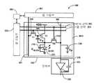
도 3a는 픽셀(200)을 구동하기 위하여 사용될 수 있는 단순화된 픽셀 회로(300)에 대한 구조를 도시한 것이다. 트랜지스터(305)는 픽셀(200)(도 2에 도시됨)를 턴온하는 스위치로서 동작한다. 구동 전류는 트랜지스터(305)를 통과하여 픽셀(200)의 출력을 구동한다.3A shows a structure for a
도 3b는 단순화된 픽셀 회로(301a)에 대한 구조를 도시한 것이며, 상기 단순화된 픽셀 회로(301a)는 본 발명의 방법에 따라 수정되었다. 판독부(315)는 스위치(310a)를 통해 도 3a의 픽셀 회로(300)과 연결된다. 판독부(315)는 픽셀(200)의 커패시턴스(210)가 결정되도록 한다. 판독부(315)는 판독부 커패시터(325)와 병렬로 연결된 연산 증폭기(320)를 구비한다. 이러한 구성은 충전 증폭기(charge amplifier)로서 언급될 것이다. 또한 상기 회로는 내재적인(inherent) 기생 커패시턴스(330)을 갖는다. 판독부(315)의 상기 회로 요소들은 디스플레이 패널의 후면 전자 소자들에 구현될 것이다. 선택적으로, 상기 판독부 구성 요소들은 상기 디스플레이 패널에서 분리되어 구현될 수 있을 것이다. 판독부(315)의 다른 실시 형태는 디스플레이의 행 구동 회로들에 합체된다.3B shows a structure for a
만약 판독부(315)) 회로가 디스플레이 패널의 후면 회로부로부터 분리되어 구현되는 경우, 스위치(310a)는 후면 전자 소자들에 구현될 것이다. 선택적으로, 상기 스위치(310a)는 또한 상기 분리된 판독부(315)에 구현될 수도 있을 것이다. 만약 스위치(310a)가 상기 분리된 판독부(315)에 구현되는 경우, 스위치(310a)와 픽셀 회로(300)의 사이에 전기적 연결이 제공되어야만 한다.If the
도 3c는 명확한 설명을 위하여 단일의 픽셀 회로(301b)를 구비하는 디스플레이(390)의 구조를 도시한 것이다. 디스플레이(390)는 열 구동부(370), 행 구동부(360), 제어부(380), 디스플레이 패널(350) 및 판독부(315)를 구비한다. 판독부(315)는 분리된 구성요소로서 도시된다. 앞서 설명한 바와 같이, 판독부 회로들은 디스플레이(390)의 다른 구성 요소들과 합체될 수 있을 것이다.3C illustrates the structure of a
도 3b에 도시된 픽셀(200)의 구동을 제어하는 단일의 트랜시스터(305)는 2개의 트랜지스터들에 의해 대체된다. 제1 트랜지스터 T1(335)는 열 구동부들(370)에 의해 제어되는 스위칭 트랜지스터로서 동작한다. 제2 트랜지스터 T2(340)는 픽셀(200)에 적정 전류를 공급하기 위한 구동 트랜지스터로서 동작한다. T1(335)이 턴온되면, 행 구동부들(360)이 트랜지스터 T2(340)을 통해 구동 전류(휘도 열화가 보상된)로 픽셀 회로(301b)의 픽셀을 구동하도록 한다. 도 3b의 스위치(310a)는 트랜지스터 T3(310b)와 대체된다. 제어부(380)는 트랜지스터 T3(310b)를 제어한다. 트랜지스터 T3(310b)는 턴온 및 턴오프되어 판독부(315)를 픽셀 회로들과 전기적으로 연결시킬 수 있다.The
열 선택(353) 및 판독 선택(352) 라인들은 열 구동부(370)에 의해 구동될 수 있다. 열 선택 라인(353)은 픽셀의 열이 온 될 때 제어한다. 판독 선택 라인(The Read Select line 352)는 판독부(315)와 픽셀 회로를 연결하는 스위치(트랜지스터 T3)(310)을 제어한다. 행 구동 라인(361)은 행 구동부(360)에 의해 구동된다. 행 구동 라인(Column Driver line;361)은 픽셀(200) 밝기를 구동하기 위한 상기 보상된 구동 전류를 제공한다. 또한, 상기 픽셀 회로는 판독부 라인(356)을 구비한다. 상기 픽셀 회로는 트랜지스터 T3(310b)에 의해 판독부 라인(356)과 연결된다. 판독부 라인(356)은 픽셀 회로를 판독부(315)와 연결한다.The column select 353 and read select 352 lines may be driven by the
상기 디스플레이(390)의 상기 제어부(380)는 디스플레이(390)의 다양한 블록들의 기능을 제어한다. 상기 행 구동부(360)은 픽셀(200)에 구동 전류를 제공한다. 픽셀(200)을 구동하기 위하여 사용되는 전류는 픽셀(200)의 밝기를 결정하는 것이 분명할 것이다. 열 구동부들(370)은 픽셀들의 열이 특정 시간에 행 구동부들(360)에 의해 구동될 것을 결정한다. 제어부(380)는 행(360) 및 열(370) 구동부들 조정하여, 픽셀들의 열이 적정한 시간에 적정 전류에 의해 턴 온되어 구동되도록 하여 원하는 출력을 만들어낸다. 열(370) 및 행 구동부들(360)을 제어함으로써(예를 들면, 특정 열이 턴온될 때 및 전류가 상기 열의 각 픽셀을 구동하는 것) 제어부(380)는 디스플레이 패널(350)의 전반적인 기능들을 제어한다.The
도 3c의 디스플레이(390)는 적어도 2개의 모드에서 동작될 수 있다. 제1 모드는 일반적인 디스플레이 모드이며, 이 모드에서는 제어부(380)가 열(370) 및 행 구동부들(360)을 제어하여 적정 출력을 디스플레이하는 픽셀들(200)을 구동한다. 상기 디스플레이 모드에서, 제어부(380)가 트랜지스터 T3(310b)를 제어하여 트랜지스터 T3(310b)를 오프시킴으로써, 판독부(315)는 픽셀 회로들과 전기적으로 연결되지 않도록 한다. 제2 모드는 판독 모드이며, 이 모드에서는 제어부(380)가 판독부(315)를 제어하여 픽셀(200)의 커패시턴스를 결정한다. 상기 판독 모드에 있어서, 상기 제어부(380)는 필요할 때 트랜지스터 T3(310b)를 턴 온 및 턴 오프한다.The
도 4는 흐름도(400)를 도시한 것으로서, 상기 흐름도에는 픽셀의 휘도 열화를 설명하여 상기 픽셀을 보상된 전류로 구동하는 단계들을 보여준다. 단계 405에서 상기 픽셀의 커패시턴스가 결정된다. 다음, 단계 410에서, 상기 결정된 커패시턴스는 전류 보정 상수와 상관(correlation)된다. 단계 415에서, 상기 상관은 다양한 방법으로 행해지는데, 그 예로서 픽셀 형태의 노화를 모델링하는 방정식을 풀거나 커패시턴스를 전류 보정 상수와 직접 상관시키는 룩업 수단들을 통해서 행해진다.4 illustrates a flow diagram 400, which illustrates the steps of driving the pixel with a compensated current by explaining the luminance degradation of the pixel. In
도 3c에 도시된 바와 같이, 디스플레이의 픽셀의 커패시턴스를 결정하는 경우, 상기 스위치는 초기에는 닫혀지며(트랜지스터 T3(310b)는 온 된다.), 판독부 라인(356)을 통해 픽셀 회로를 판독부(315)와 전기적으로 연결하고, 픽셀의 커패시턴스(210)가 판독부(315)(예: 충전 증폭기)의 바이어스 전압들에 의해 결정되는 초기 전압 V1으로 충전된다. 다음, 상기 스위치는 오픈되어(트랜지스터 T3가 턴오프된다.), 픽셀 회로를 판독부 라인(356)으로부터 분리시키고, 다음 판독부(315)로부터 분리시킨다. 다음, 판독부(315)(또는 판독부 라인(356))의 기생 커패시턴스(330)가 다른 전압 V2로 충전되는데, 상기 V2는 판독부(315)(즉, 충전 증폭기)의 바이어스 전압에 의해 결정된다. 판독부(315)(즉, 충전 증폭기)의 상기 바이어스 전압은 제어부(380)에 의해 제어되며, 그 결과 픽셀 커패시턴스(210)을 충전하는데 사용되는 전압과 서로 다르게 될 것이다. 최종적으로, 상기 스위치는 다시 닫혀져서 판독부(315)가 픽셀 회로에 전기적으로 연결된다. 다음, 상기 픽셀 커패시턴스(210)는 V2로 충전된다. Coled에서 전압이 V1에서 V2로 변화되기 위하여 요구되는 전하량은 전압으로서 판독될 수 있는 판독 커패시터(325)에 저장된다.As shown in FIG. 3C, when determining the capacitance of a pixel of the display, the switch is initially closed (transistor T3 310b is turned on), and the pixel circuit is read through
전술한 방법의 정확성은 상기 기생 커패시턴스(330)가 전압 V2로 충전되는 시간과 스위치(310)이 닫혀져 판독부(315)가 픽셀 회로에 전기적으로 연결되는 시간의 사이의 수 마이크로 초(seconds)동안 대기함에 의해 증가될 수 있다. 상기 수 마이크로 초가 지난 후, 판독 커패시터(315)의 누설 전류가 측정될 수 있으며, 그 결과로서 생기는 전압은 판독 커패시터(315)에 걸쳐 나타내는 최종 전압으로부터 결정되고 유도된다.The accuracy of the method described above is several microseconds between the time when the
일단 스위치(310)이 닫혀지면, 판독 커패시터(3145)에 대한 전압의 변화는 측정된다. 픽셀커패시턴스(210) 및 기생 커패시턴스(330)가 동일한 전압으로 충전되면, 판독 커패시터(325)에 대한 전압 변화는 픽셀(200)의 커패시턴스(210)를 결정하기 위하여 사용될 수 있다. 상기 판독 커패시터(325)에 대한 전압 변화는 아래의 수학식 1에 따라 변화된다.Once switch 310 is closed, the change in voltage for read capacitor 3145 is measured. If

여기서,
Coled는 상기 픽셀 (이 경우 OLED)의 상기 커패시턴스(210)이다;Coled is the
Cread는 상기 판독 커패시터(325)의 상기 커패시턴스이다;Cread is the capacitance of the
V1은 상기 픽셀 커패시턴스(210)가 초기에 충전되는 전압이다; 그리고,V1 is the voltage at which the
V2는 상기 스위치가 열렸을 때 상기 기생 패시턴스(330)가 충전되는 전압이다.V2 is a voltage at which the
상기 전압들 V1 및 V2는 상기 제어부(380)에 의해 알려질 것이고 제어될 것이다. Cread는 특정의 회로 설계 요구 조건들과 일치하도록 요구됨에 따라 알려지고 선택될 것이다.

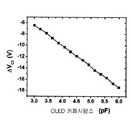
도 5는, 그래프에서, 전술한 상기 판독부(315) 회로를 사용하여 상기 판독 커패시터(325)에 대한 전압에서의 시뮬레이팅된 변화를 보여준다. 상기 그래프로부터, 상기 판독부(315)가 상기 판독 커패시터(325)에 대한 상기 측정된 전압 변화에기초하여 상기 픽셀(200)의 상기 커패시턴스(210)를 결정할 수 있음이 명백하다.5 shows a simulated change in voltage for the
일단 상기 픽셀(200)의 상기 커패시턴스(210)가 결정되면, 상기 픽셀(200)의 상기 나이를 결정할 수 있다. 전술한 바와 마찬가지로, 상기 커패시턴스(210)와 픽셀(200)의 나이의 사이의 상기 관계는 서로 다른 픽셀 타입들에 대하여 주어진 전 류에 대해 픽셀들이 스트레싱하고 주기적으로 픽셀의 상기 커패시턴스를 측정함에 의해 실험적으로 결정될 수 있다. 상기 커패시턴스 및 픽셀의 나이 사이의 특별한 관계는 서로 다른 픽셀 타입들과 크기들에 대하여 변화할 것이고, 상기 커패시턴스 및 상기 픽셀의 나이의 사이에 만들어질 수 있는 적정의 상관(correlation)을 확인함으로써 실험적으로 결정될 수 있을 것이다.Once the
상기 판독부(315)는 상기 연산 증폭기(320)의 출력으로부터 상기 픽셀(200)의 상기 커패시턴스(210)를 결정하는 회로를 포함할 수 있다. 다음, 이 정보는 상기 픽셀(200)의 전류 보정 상수를 결정하는 상기 제어부(380)에 제공될 수 있을 것이다. 선택적으로, 상기 판독부(315)의 상기 연산 증폭기(320)의 상기 출력은 상기 제어부(380)의 후면으로 제공될 수 있다. 이 경우, 상기 제어부(380)는 상기 픽셀(200)의 상기 커패시턴스(210) 및 상기 결과로 생기는 전류 보정 상수를 결정하기 위하여 필요한 회로들과 로직(logic)를 구비한다.The
도 6은, 그래프에서, 노화의 전후의 상기 픽셀의 커패시턴스 및 전압을 보여준다. 상기 노화는 일주일동안 20mA/cm2의 일정한 전류로 픽셀을 스트레싱함에 의해 발생된다. 상기 커패시턴스는 나이에 선형적으로 관련된다. 다항식(polynomial) 관계와 같은 다른 관계들이 또한 가능하다. 상기 관계는 단지 실험적인 측정들에 의해 정확하게 표현될 수 있을 것이다. 이 경우, 상기 커패시턴스-나이 특성들에 대한 모델링이 정확하다는 것을 확인하기 위하여, 추가적인 측정들이 요구된다.6 shows, in the graph, the capacitance and voltage of the pixel before and after aging. The aging is caused by stretching the pixels at a constant current of 20 mA /
도 7은, 그래프에서, 상기 휘도와 픽셀의 나이 사이의 관계를 보여준다. 이 관계는 상기 픽셀의 상기 커패시턴스를 결정할 때 실험적으로 결정될 수 있다. 상 기 픽셀의 나이 및 주어진 휘도를 만들기 위하여 요구되는 전류 사이의 상기 관계도 또한 실험적으로 결정될 수 있다. 다음, 상기 픽셀의 나이 및 주어진 휘도를 만들기 위하여 요구되는 전류 사이의 상기 결정된 관계는 디스플레이에서 상기 픽셀의 노화를 보상하기 위하여 사용될 수 있다.Figure 7 shows the relationship between the luminance and the age of the pixels in the graph. This relationship can be determined experimentally when determining the capacitance of the pixel. The relationship between the age of the pixel and the current required to produce a given brightness can also be determined experimentally. Next, the determined relationship between the age of the pixel and the current required to produce a given brightness can be used to compensate for the aging of the pixel in the display.
전류 보정 상수는 상기 원하는 휘도를 만들기 위하여 픽셀을 구동하는 적정 전류를 결정하기 위하여 사용될 수 있다. 예를 들면, 노화(예를 들면 2주동안 15mA/cm2의 전류로 그것을 구동함에 의해)된 픽셀에서 새로운 픽셀의 휘도와 동일한 휘도를 만들기 위하여, 상기 노화된 픽셀은 상기 전류의 1.5배로 구동되어야만 한다는 것이 실험적으로 결정될 수 있다. 2개의 서로 다른 나이에서 주어진 휘도를 위하여 요구되는 전류들을 결정하고 상기 노화는 선형 관계가 있음을 가정할 수 있다. 이로부터, 상기 전류 보정 상수는 서로 다른 나이들에 대하여 외삽법에 의해 추정될 수 있다(extrapolatte). 게다가, 상기 전류 보정 상수는 주어진 나이의 픽셀에 대한 서로 다른 휘도 레벨들에서 동일하다고 가정될 수 있다. 즉, 주어진 나이의 픽셀에 대하여 X cd/m2의 휘도를 만들기 위하여 1.1의 전류 보정 상수가 요구되고 2X cd/m2의 휘도를 만들기 위하여도 1.1의 전류 보정 상수가 요구된다. 이러한 가정들을 세우는 것은 실험적으로 결정될 것이 요구되는 측정량을 감소한다.The current correction constant can be used to determine the appropriate current driving the pixel to produce the desired brightness. For example, to produce the same luminance as that of a new pixel in an aged pixel (eg by driving it at a current of 15 mA /
추가정인 정보는 실험적으로 결정될 것이며, 이는 많은 가정들처럼 의존하지는 않는 결과를 갖게 된다. 예를 들면, 상기 픽셀 커패시턴스(210)은 4개의 서로 다른 픽셀 나이들에서 결정될 수 있다(적정의 정확성을 부여하기 위하여 요구되는 만큼 많은 나이들에서 상기 커패시턴스는 결정될 수 있을 것이라는 것이 이해된다 ). 다음, 상기 노화 과정은 더욱 정확하게 모델링될 것이고, 그 결과로서 상기 추정된 나이가 더욱 정확하게 될 것이다. 게다가, 주어진 나이의 픽셀에 대한 전류 보정 상수는 서로 다른 휘도 레벨들에 대하여 결정될 것이다. 또한, 상기 추가의 측정들은 상기 노화 및 전류 보정 상수의 모델링을 더욱 정확하게 만든다.Additional qualification information will be determined experimentally, which has consequences that do not depend on many assumptions. For example, the
실험적으로 포함되는 정보의 양은 측정을 하기 위하여 필요한 시간과 제공되는 측정이 제공하는 추가의 정확성의 사이의 교환 조건(a trade off)가 될 것이라는 것이 명백하다.It is clear that the amount of information included experimentally will be a trade off between the time needed to make the measurement and the additional accuracy provided by the measurement provided.
도 8은 블록도에서 디스플레이(395)를 보여준다. 상기 디스플레이(395)는 디스플레이 패널(350), 열 구동부(370), 행 구동부(360) 및 제어부(380)를 구비한다. 상기 디스플레이 패널(350)은 열과 행으로 정렬된 픽셀 회로들(301b)의 배열체(an array)로 이루어진다. 도 8에 도시된 상기 디스플레이 패널(350)의 픽셀 회로들(301a)은 도 3c에 도시되고 전술된 것과 같이 구현된다. 전형적인 디스플레이 모드에 있어서, 트랜지스터 T3(310b)가 오프되면, 상기 제어부(380)가 상기 열 구동부(370)를 제어하여 판독 선택 라인(352)를 구동시켜 트랜지스터 T3(310b)를 턴 오프되도록 한다. 상기 제어부(380)는 상기 열 구동부(370)를 제어하여, 상기 열 구동부(370)가 적정 열의 열 선택 라인(353)을 구동하여 픽셀 열을 턴온되도록 한다. 다음, 상기 제어부(380)는 행 구동부(360)을 제어하여 적정 전류가 픽셀의 행 구동 라인(361)을 구동되도록 한다. 상기 제어부(380)는 주기적으로, 예를 들면 1초당 60번, 상기 디스플레이 패널(350)의 각 열을 리플래쉬시킨다.8 shows a
상기 디스플레이(395)가 판독 모드(the read mode)인 경우, 상기 제어 부(380)는 상기 열 구동부(370)를 제어하여, 그것이 판독 선택 라인(352)(상기 스위치, 트랜지스터 T3(310)을 턴온 및 오프하기 위한) 및 상기 커패시턴스들을 충전하기 위한 상기 판독부(315)의 상기 바이어스 전압(따라서, 상기 판독부 라인(356)의 전압)을 전술한 바와 같이 픽셀 (200)의 커패시턴스(210)을 결정하기 위하여 필요한 만큼의 V1 및 V2로 구동한다. 상기 제어부(380)는 특정 열에서 픽셀 회로(301b)의 각 픽셀(200)의 상기 커패시턴스(210)를 결정하기 위한 판독 동작을 수행한다. 다음, 상기 제어부는 이 정보들을 사용하여 상기 픽셀의 나이 및 상기 구동 전류에 인가되는 전류 보정 상수를 교대로 결정한다.When the
구동부(360, 370) 및 판독부(315)를 제어하는 로직들뿐만 아니라, 상기 판독부(315)에서 결정되는 것과 마찬가지로, 상기 제어부(380)는 상기 커패시턴스(210)에 기초하여 상기 전류 보정 상수들을 결정하는 로직들을 또한 구비한다. 전술한 바와 같이, 상기 전류 보정 상수는 다른 기술들을 사용하여 결정될 수 있다. 예를 들면, 만약 픽셀이 초기 커패시턴스 및 일주일 동안의 노화후의 커패시턴스를 결정하기 위하여 측정되는 경우, 상기 제어부(380)는 상기 2개의 측정된 커패시턴스들 및 나이들에 의하여 결정되는 선형 방정식을 푸는 과정에 의해 특정 커패시턴스의 나이를 결정하도록 채택될 수 있다. 만약 상기 요구되는 전류 보정 상수가 각 레벨에서 단일의 휘도에 대하여 측정되는 경우, 상기 전류 보정 상수는 특정의 픽셀 나이에 대한 전류 보정 상수가 주어진 룩업 테이블(look-up table)을 사용하여 픽셀에 대하여 결정될 수 있을 것이다. 상기 제어부(380)는 픽셀의 커패시턴스(210)를 상기 판독부(315)로부터 수신하고 상기 픽셀의 서로 다른 나이들에 대한 상기 2개 의 측정된 커패시턴스들에 의하여 결정되는 선형 방정식을 풀음으로써 상기 픽셀의 나이를 결정할 수 있을 것이다. 상기 결정된 나이로부터, 상기 제어부(315)는 룩업 테이블을 사용하여 픽셀에 대한 전류 보정 상수를 결정한다.In addition to the logics controlling the
만약 픽셀 노화 과정에 대한 추가의 측정들이 행해진다면, 다음 상기 픽셀의 나이를 결정하는 것은 선형 방정식을 푸는 것처럼 쉽지는 않을 것이다. 예를 들면, 만약 3개의 점들 P1, P2, 및 P3가 상기 노화 과정동안 취해지고 상기 노화가 점 P1및 P2의 사이에서는 선형적이지만 점 P2 및 P3의 사이에는 지수함수적이거나 비선형적인 경우, 상기 픽셀의 나이를 결정하는 것은 먼저 상기 커패시턴스가 존재하는 범위(즉, P1-P2, 또는 P2-P3 사이)를 결정하고 그 다음 적절한 나이를 결정해야 할 필요가 있을 것이다.If further measurements of the pixel aging process are made, then determining the age of the pixel will not be as easy as solving a linear equation. For example, if three points P1, P2, and P3 are taken during the aging process and the aging is linear between points P1 and P2 but exponential or nonlinear between points P2 and P3, Determining the age of a pixel will need to first determine the range in which the capacitance is present (ie, between P1-P2, or P2-P3) and then determine the appropriate age.
상기 픽셀의 나이를 결정하기 위하여 상기 제어부(380)에 의하여 사용되는 방법은 디스플레이 장치의 요구 조건들에 따라 다양할 것이다. 상기 제어부(380) 가 상기 픽셀 나이 및 그렇게 하기 위하여 필요한 정보들을 결정하는 방법은 제어부의 로직들로 프로그램될 것이다. 상기 요구되는 로직은 ASIC(Application Specific Integrated Circuit)와 같은 하드웨어로 구현될 수 있으며, 이런 경우 상기 제어부(380)가 상기 픽셀 나이를 결정하는 방법을 변화시키는 것은 더욱 어려울 것이다. 상기 제어부(380)가 상기 픽셀의 나이를 결정하는 방법을 수정하는 것이 더 쉽도록 하기 위하여, 상기 요구되는 로직은 하드웨어 및 소프트웨어의 조합으로 구현될 수 있다.The method used by the
상기 커패시턴스를 나이와 상관시키는 다양한 방법들외에도, 상기 제어 부(380)는 다양한 방법으로 상기 전류 보정 상수를 결정할 것이다. 앞서 설명한 바와 마찬가지로, 전류 보정 상수들은 다양한 휘도 레벨들에 대하여 결정될 수 있을 것이다. 상기 나이-커패시턴스 상관 관계와 같이, 특정 휘도 레벨에 대한 상기 전류 보정 상수는 가능한 측정들로부터 추정될 수 있을 것이다. 상기 커패시턴스-나이의 상관 관계와 유사하게도, 상기 제어부(380)가 상기 전류 보정 상수를 결정하는 방법에 대한 세부적인 것은 변할 것이고, 상기 전류 보정 상수를 결정하기 위하여 필요한 로직들은 하드웨어 또는 소프트웨어 중의 하나로 상기 제어부(380)로 프로그램될 수 있을 것이다.In addition to various methods of correlating the capacitance with age, the
일단 픽셀에 대한 전류 보정 상수가 결정되면, 그것은 필요할 때 상기 구동 전류를 스케일(scale)하기 위하여 사용된다.Once the current correction constant for the pixel is determined, it is used to scale the drive current when needed.
도 9는 블록도에서 디스플레이(398)의 구현예를 보여준다. 도 8을 참조하여 앞서 설명된 상기 디스플레이(390)는 픽셀 타입에 대하여 공통인 픽셀 특성들에 대하여 보정하기 위하여 수정될 것이다. 예를 들면, 픽셀들의 특성들은 동작 환경의 온도에 의존한다고 알려져 있다. 노화의 결과인 커패시턴스를 결정하기 위하여, 상기 디스플레이(398)은 픽셀들(396)의 추가의 열이 제공된다. 이러한 픽셀들(396)은 이하 기초 픽셀들(base pixels)로서 언급되는데, 디스플레이 전류들에 의해 구동되지 않고, 그 결과로서 그것들은 디스플레이 픽셀들이 겪는 노화를 겪지 않게 된다. 상기 기초 픽셀들(396)은 그것들의 커패시턴스를 결정하기 위하여 상기 판독부(315)에 연결될 것이다. 상기 픽셀 커패시턴스를 직접적으로 사용하는 것을 대신하여, 상기 제어부(380)는 상기 디스플레이 픽셀의 나이를 결정할 때 사용하기 위 한 상기 커패시턴스로서, 상기 픽셀 커패시턴스(210) 및 상기 기초 커패시턴스의 사이의 차이값을 사용할 것이다.9 shows an implementation of
이것은 다른 보정들을 함께 쉽게 결합하는 능력을 제공한다. 상기 픽셀의 나이는 상기 기초 픽셀 커패시턴스에 대하여 설명되도록 보정된 커패시턴스에 기초하여 결정되므로, 상기 나이 보정 상수는 비-노화 요인들에 대한 보정은 포함하지 않는다. 예를 들면, 전류 보정 상수는 2개의 전류 보정 상수들의 합으로 결정될 수 있을 것이다. 첫번째는 앞서 설명한 나이-관련된 전류 보정 상수가 될 것이다. 두번째는 보정 상수에 관련된 동작 환경 온도일 것이다.This provides the ability to easily combine different corrections together. Since the age of the pixel is determined based on the corrected capacitance to be described with respect to the elementary pixel capacitance, the age correction constant does not include correction for non-aging factors. For example, the current correction constant may be determined as the sum of the two current correction constants. The first would be the age-related current correction constant described above. The second would be the operating environment temperature relative to the correction constant.
상기 제어부(380)는 다양한 주파수들에서 판독 동작(즉, 판독 모드에서 동작)을 실행할 수 있다. 예를 들면, 판독 동작은 디스플레이의 프레임이 리플레쉬되는 모든 시간마다 실행될 수 있을 것이다. 판독 동작을 실행하기 위하여 필요한 시간은 구성 요소들에 의해 결정된다는 것은 분명하다. 예를 들면, 원하는 전압으로 충전되는 상기 커패시턴스들에 대하여 필요한 안정화 시간(the settling time)은 커패시터들의 크기에 의존한다. 만약 상기 시간이 디스플레이의 프레임 리플래쉬율에 비하여 큰 경우, 상기 프레임이 리플래쉬되는 각 시간에 판독을 수행하는 것이 가능하지 않게 될 것이다. 이 경우, 제어부는 판독을, 예를 들면 디스플레이가 턴온 또는 오프될 때 실행할 것이다. 만약 상기 판독 시간이 리플래쉬 율과 비교될 수 있다면, 1초마다 판독 동작이 실행되는 것이 가능할 것이다. 이것은 블랭크 프레임(blank frame)을 각 디스플레이로 모든 60 프레임들마다 삽입할 수 있다. 그런데, 이것은 디스플레이의 질을 열화시키지 않을 것이다. 상기 판독 동작들의 주파 수는 적어도 디스플레이를 구성하는 요소들 및 상기 요구되는 디스플레이 특성들(예를 들면, 프레임율)에 의존된다. 상기 판독 시간(the read time)이 리플래쉬율과 비교하여 짧은 경우, 상기 디스플레이 모드에서 상기 픽셀을 구동하기전에 판독이 실행될 것이다.The
상기 판독부(315)는 열에서 단일의 픽셀(200)의 커패시턴스(210)를 결정하는 것으로서 위에서 설명하였다. 단일의 판독부(315)는 열에서 복수 개의 픽셀들의 커패시턴스를 결정하도록 수정될 수 있다 이것은 스위치(도시되어 있지 않음)를 포함하여 상기 판독부(315)가 연결되는 픽셀 회로(301b)를 결정함으로써 성취될 수 있을 것이다. 상기 스위치는 상기 제어부(380)에 의해 제어될 수 있을 것이다. 더 나아가, 비록 단일의 판독부(315)가 설명되었지만, 그것은 단일의 디스플레이에 대한 다중 판독부들을 가질 수 있다. 만약 다중 판독부들이 사용된다면, 각 개별 판독부들은 판독부 구성요소들로서 언급될 수 있으며, 다중 판독부의 요소들의 그룹은 판독부로서 언급될 수 있을 것이다.The
비록 위에서 픽셀(200)의 상기 커패시턴스(210)를 결정하기 위한 회로를 설명하였지만, 다음 회로들이나 방법들이 상기 픽셀 커패시턴스(210)를 결정하기 위하여 사용될 수 있음은 분명하다. 예를 들면, 상기 판독부(315)의 상기 전압 증폭기 구성을 대신하여, transresistance 증폭기가 상기 상기 픽셀의 상기 커패시턴스를 결정하기 위하여 사용될 수 있을 것이다. 이런 경우, 상기 픽셀의 커패시턴스 및 상기 기생 커패시턴스는 램프(ramp) 또는 정현파(sinusoidal) 신호와 같은 변화되는 전압 신호를 사용하여 충전된다. 그 결과로 생기는 전류가 측정되고 상기 커 패시턴스가 결정될 수 있다.Although the circuitry for determining the
상기 커패시턴스가 기생 커패시턴스(330) 및 상기 픽셀 커패시턴스(210)의 결합이므로, 상기 기생 커패시턴스(330)는 상기 픽셀 커패시턴스(210)를 결정하기 위해서는 알고 있어야만 한다. 상기 기생 커패시턴스(330)는 직접 측정에 의해 결정될 수 있다. 선택적으로 또는 부가적으로, 상기 기생 커패시턴스(330)는 상기 transresistance 증폭기 구성 판독부를 사용하여 결정될 수 있다. 스위치는 상기 픽셀 회로를 상기 판독부로부터 분리시킬 수 있다. 다음, 상기 기생 커패시턴스(330)는 그것을 변화되는 전압 신호로 충전시키고 그 결과로서 생기는 전류를 측정함에 의해 결정될 수 있을 것이다.Since the capacitance is a combination of the
전기적인 노화로 인한 픽셀들의 휘도 레벨을 보상하기 위하여 본 명세서에서 설명된 구현예들은 디스플레이의 수율, 개구율(aperture ratio) 또는 해상도를 감소시킴없이 디스플레이 패널에 유리하게 포함될 수 있을 것이다. 이러한 기술을 구현하기 위하여 필요한 전자 장비들은 디스플레이의 크기 또는 필요 소비 전력들을 크게 증가시키지 않으면서 상기 디스플레이에 의해 요구되는 전자 장비들에 쉽게 포함될 수 있을 것이다.Embodiments described herein to compensate for the luminance level of pixels due to electrical aging may be advantageously included in the display panel without reducing the yield, aperture ratio or resolution of the display. The electronic equipment required to implement this technique may be easily included in the electronic equipment required by the display without significantly increasing the size or power consumption of the display.
주로 설명된 하나 또는 그 이상의 구현예들은 예로서 설명되었다. 특허 청구 범위에 한정된 본 발명의 범위로부터 벗어남없이 다양한 변화나 수정들이 이루어질 수 있음은 당업자에게 자명하다.One or more embodiments that have been described primarily have been described by way of example. It will be apparent to those skilled in the art that various changes or modifications can be made without departing from the scope of the invention as defined by the claims.
도 1은 유기 발광 다이오드의 구조를 도시한 블록도이다.1 is a block diagram showing the structure of an organic light emitting diode.
도 2는 OLED 픽셀의 회로 모델을 구조적으로 도시한 것이다.2 structurally illustrates a circuit model of an OLED pixel.
도 3a는 디스플레이에 사용될 수 있는 단순화된 픽셀 회로를 구조적으로 도시한 것이다.3A structurally illustrates a simplified pixel circuit that can be used in a display.
도 3b는 수정되고 단순화된 픽셀 회로를 구조적으로 도시한 것이다.3B structurally illustrates a modified and simplified pixel circuit.
도 3c는 단일의 픽셀을 구비하는 디스플레이를 구조적으로 도시한 것이다.3C structurally illustrates a display with a single pixel.
도 4는 픽셀의 휘도 열화를 설명하기 위하여 보상된 전류로 픽셀을 구동하는 단계들을 도시한 흐름도이다.4 is a flowchart illustrating steps of driving a pixel with a compensated current to account for the luminance deterioration of the pixel.
도 5는 상기 판독부 회로를 사용하여 상기 판독 커패시터에 대한 전압의 시뮬레이팅된 변화를 도시한 그래프이다.5 is a graph illustrating a simulated change in voltage for the read capacitor using the readout circuit.
도 6은 서로 나이에 대한 커패시턴스 및 픽셀의 전압 사이의 관계를 도시한 그래프이다.Fig. 6 is a graph showing the relationship between capacitance and voltage of pixels with respect to each other.
도 7은 상기 휘도 및 픽셀의 노화 사이의 관계를 도시한 그래프이다.7 is a graph showing the relationship between the luminance and the aging of the pixel.
도 8은 디스플레이를 도시한 블록도이다. 그리고, 도 9는 디스플레이의 구현예를 도시한 블록도이다.8 is a block diagram illustrating a display. 9 is a block diagram illustrating an embodiment of a display.
Claims (19)
Translated fromKorean

Applications Claiming Priority (2)
| Application Number | Priority Date | Filing Date | Title |
|---|---|---|---|
| CA002556961ACA2556961A1 (en) | 2006-08-15 | 2006-08-15 | Oled compensation technique based on oled capacitance |
| CA2,556,961 | 2006-08-15 |
Publications (1)
| Publication Number | Publication Date |
|---|---|
| KR20090063207Atrue KR20090063207A (en) | 2009-06-17 |
Family
ID=39081871
Family Applications (1)
| Application Number | Title | Priority Date | Filing Date |
|---|---|---|---|
| KR1020097002992AWithdrawnKR20090063207A (en) | 2006-08-15 | 2007-08-15 | Compensation method for organic light emitting diode luminance deterioration |
Country Status (8)
| Country | Link |
|---|---|
| US (6) | US8026876B2 (en) |
| EP (1) | EP2074609A4 (en) |
| JP (1) | JP5535627B2 (en) |
| KR (1) | KR20090063207A (en) |
| CN (1) | CN101523470B (en) |
| CA (1) | CA2556961A1 (en) |
| TW (1) | TW200816147A (en) |
| WO (1) | WO2008019487A1 (en) |
Cited By (6)
| Publication number | Priority date | Publication date | Assignee | Title |
|---|---|---|---|---|
| KR20150016030A (en)* | 2013-08-02 | 2015-02-11 | 삼성디스플레이 주식회사 | Method and apparatus for measuring capacitance of organic light emitting device |
| KR20160007971A (en)* | 2014-07-10 | 2016-01-21 | 엘지디스플레이 주식회사 | Organic Light Emitting Display For Sensing Degradation Of Organic Light Emitting Diode |
| KR20160037105A (en)* | 2014-09-26 | 2016-04-05 | 가부시키가이샤 한도오따이 에네루기 켄큐쇼 | Display device and driving method thereof |
| KR20180059604A (en)* | 2016-11-25 | 2018-06-05 | 엘지디스플레이 주식회사 | Organic light emitting display device and method for drving the same |
| US10186195B2 (en) | 2015-04-03 | 2019-01-22 | Samsung Display Co., Ltd. | Organic light emitting display device and driving method thereof |
| KR20200019321A (en) | 2018-08-14 | 2020-02-24 | 삼성전자주식회사 | Device for compensating for degradation and organic light emitting display comprising the device |
Families Citing this family (123)
| Publication number | Priority date | Publication date | Assignee | Title |
|---|---|---|---|---|
| CA2443206A1 (en) | 2003-09-23 | 2005-03-23 | Ignis Innovation Inc. | Amoled display backplanes - pixel driver circuits, array architecture, and external compensation |
| CA2472671A1 (en) | 2004-06-29 | 2005-12-29 | Ignis Innovation Inc. | Voltage-programming scheme for current-driven amoled displays |
| US10012678B2 (en) | 2004-12-15 | 2018-07-03 | Ignis Innovation Inc. | Method and system for programming, calibrating and/or compensating, and driving an LED display |
| US8576217B2 (en) | 2011-05-20 | 2013-11-05 | Ignis Innovation Inc. | System and methods for extraction of threshold and mobility parameters in AMOLED displays |
| US10013907B2 (en) | 2004-12-15 | 2018-07-03 | Ignis Innovation Inc. | Method and system for programming, calibrating and/or compensating, and driving an LED display |
| US8599191B2 (en) | 2011-05-20 | 2013-12-03 | Ignis Innovation Inc. | System and methods for extraction of threshold and mobility parameters in AMOLED displays |
| US9280933B2 (en) | 2004-12-15 | 2016-03-08 | Ignis Innovation Inc. | System and methods for extraction of threshold and mobility parameters in AMOLED displays |
| US9171500B2 (en) | 2011-05-20 | 2015-10-27 | Ignis Innovation Inc. | System and methods for extraction of parasitic parameters in AMOLED displays |
| US9275579B2 (en) | 2004-12-15 | 2016-03-01 | Ignis Innovation Inc. | System and methods for extraction of threshold and mobility parameters in AMOLED displays |
| US20140111567A1 (en) | 2005-04-12 | 2014-04-24 | Ignis Innovation Inc. | System and method for compensation of non-uniformities in light emitting device displays |
| US9799246B2 (en) | 2011-05-20 | 2017-10-24 | Ignis Innovation Inc. | System and methods for extraction of threshold and mobility parameters in AMOLED displays |
| TWI402790B (en) | 2004-12-15 | 2013-07-21 | Ignis Innovation Inc | Method and system for programming, calibrating and driving a light-emitting element display |
| CA2496642A1 (en) | 2005-02-10 | 2006-08-10 | Ignis Innovation Inc. | Fast settling time driving method for organic light-emitting diode (oled) displays based on current programming |
| JP5355080B2 (en) | 2005-06-08 | 2013-11-27 | イグニス・イノベイション・インコーポレーテッド | Method and system for driving a light emitting device display |
| CA2518276A1 (en) | 2005-09-13 | 2007-03-13 | Ignis Innovation Inc. | Compensation technique for luminance degradation in electro-luminance devices |
| TW200746022A (en) | 2006-04-19 | 2007-12-16 | Ignis Innovation Inc | Stable driving scheme for active matrix displays |
| CA2556961A1 (en)* | 2006-08-15 | 2008-02-15 | Ignis Innovation Inc. | Oled compensation technique based on oled capacitance |
| US8026873B2 (en)* | 2007-12-21 | 2011-09-27 | Global Oled Technology Llc | Electroluminescent display compensated analog transistor drive signal |
| US8405585B2 (en)* | 2008-01-04 | 2013-03-26 | Chimei Innolux Corporation | OLED display, information device, and method for displaying an image in OLED display |
| KR100916913B1 (en)* | 2008-05-13 | 2009-09-09 | 삼성모바일디스플레이주식회사 | Organic light emitting display |
| JP5250493B2 (en)* | 2008-07-16 | 2013-07-31 | 株式会社半導体エネルギー研究所 | Light emitting device |
| WO2010022104A2 (en)* | 2008-08-19 | 2010-02-25 | Plextronics, Inc. | Organic light emitting diode lighting systems |
| WO2010022101A2 (en)* | 2008-08-19 | 2010-02-25 | Plextronics, Inc. | Organic light emitting diode lighting devices |
| WO2010022102A2 (en)* | 2008-08-19 | 2010-02-25 | Plextronics, Inc. | User configurable mosaic light emitting apparatus |
| WO2010022105A2 (en)* | 2008-08-19 | 2010-02-25 | Plextronics, Inc. | Organic light emitting diode products |
| EP2159783A1 (en) | 2008-09-01 | 2010-03-03 | Barco N.V. | Method and system for compensating ageing effects in light emitting diode display devices |
| US9384698B2 (en) | 2009-11-30 | 2016-07-05 | Ignis Innovation Inc. | System and methods for aging compensation in AMOLED displays |
| CA2688870A1 (en) | 2009-11-30 | 2011-05-30 | Ignis Innovation Inc. | Methode and techniques for improving display uniformity |
| US9311859B2 (en) | 2009-11-30 | 2016-04-12 | Ignis Innovation Inc. | Resetting cycle for aging compensation in AMOLED displays |
| CA2669367A1 (en) | 2009-06-16 | 2010-12-16 | Ignis Innovation Inc | Compensation technique for color shift in displays |
| US10319307B2 (en) | 2009-06-16 | 2019-06-11 | Ignis Innovation Inc. | Display system with compensation techniques and/or shared level resources |
| US10996258B2 (en) | 2009-11-30 | 2021-05-04 | Ignis Innovation Inc. | Defect detection and correction of pixel circuits for AMOLED displays |
| US8803417B2 (en) | 2009-12-01 | 2014-08-12 | Ignis Innovation Inc. | High resolution pixel architecture |
| CA2687631A1 (en) | 2009-12-06 | 2011-06-06 | Ignis Innovation Inc | Low power driving scheme for display applications |
| US10163401B2 (en)* | 2010-02-04 | 2018-12-25 | Ignis Innovation Inc. | System and methods for extracting correlation curves for an organic light emitting device |
| US20140313111A1 (en) | 2010-02-04 | 2014-10-23 | Ignis Innovation Inc. | System and methods for extracting correlation curves for an organic light emitting device |
| US10089921B2 (en) | 2010-02-04 | 2018-10-02 | Ignis Innovation Inc. | System and methods for extracting correlation curves for an organic light emitting device |
| CA2692097A1 (en) | 2010-02-04 | 2011-08-04 | Ignis Innovation Inc. | Extracting correlation curves for light emitting device |
| US10176736B2 (en) | 2010-02-04 | 2019-01-08 | Ignis Innovation Inc. | System and methods for extracting correlation curves for an organic light emitting device |
| US9881532B2 (en) | 2010-02-04 | 2018-01-30 | Ignis Innovation Inc. | System and method for extracting correlation curves for an organic light emitting device |
| CA2696778A1 (en) | 2010-03-17 | 2011-09-17 | Ignis Innovation Inc. | Lifetime, uniformity, parameter extraction methods |
| TWI428890B (en)* | 2010-10-08 | 2014-03-01 | Au Optronics Corp | Pixel circuit and display panel with ir-drop compensation function |
| US8907991B2 (en) | 2010-12-02 | 2014-12-09 | Ignis Innovation Inc. | System and methods for thermal compensation in AMOLED displays |
| US8456390B2 (en)* | 2011-01-31 | 2013-06-04 | Global Oled Technology Llc | Electroluminescent device aging compensation with multilevel drive |
| US9530349B2 (en) | 2011-05-20 | 2016-12-27 | Ignis Innovations Inc. | Charged-based compensation and parameter extraction in AMOLED displays |
| US9466240B2 (en) | 2011-05-26 | 2016-10-11 | Ignis Innovation Inc. | Adaptive feedback system for compensating for aging pixel areas with enhanced estimation speed |
| US9773439B2 (en) | 2011-05-27 | 2017-09-26 | Ignis Innovation Inc. | Systems and methods for aging compensation in AMOLED displays |
| JP2013003536A (en)* | 2011-06-21 | 2013-01-07 | Fujitsu Ltd | Display device and drive control method for display element |
| CN102915172B (en)* | 2011-08-03 | 2017-02-08 | 中兴通讯股份有限公司 | Method and device for managing display screen |
| US20130207544A1 (en)* | 2011-09-30 | 2013-08-15 | Pinebrook Imaging Technology, Ltd. | Illumination system |
| US8405086B1 (en)* | 2011-11-04 | 2013-03-26 | Shenzhen China Star Optoelectronics Technology Co., Ltd. | Pixel structure of display panel and method for manufacturing the same |
| US10089924B2 (en) | 2011-11-29 | 2018-10-02 | Ignis Innovation Inc. | Structural and low-frequency non-uniformity compensation |
| US9324268B2 (en) | 2013-03-15 | 2016-04-26 | Ignis Innovation Inc. | Amoled displays with multiple readout circuits |
| US8937632B2 (en) | 2012-02-03 | 2015-01-20 | Ignis Innovation Inc. | Driving system for active-matrix displays |
| JP2013205588A (en)* | 2012-03-28 | 2013-10-07 | Canon Inc | Light emitting device and driving method therefor |
| US9747834B2 (en) | 2012-05-11 | 2017-08-29 | Ignis Innovation Inc. | Pixel circuits including feedback capacitors and reset capacitors, and display systems therefore |
| US8922544B2 (en) | 2012-05-23 | 2014-12-30 | Ignis Innovation Inc. | Display systems with compensation for line propagation delay |
| US10008016B2 (en)* | 2012-09-05 | 2018-06-26 | Facebook, Inc. | Proximity-based image rendering |
| WO2014069324A1 (en) | 2012-10-31 | 2014-05-08 | シャープ株式会社 | Data processing device for display device, display device equipped with same and data processing method for display device |
| KR101972017B1 (en) | 2012-10-31 | 2019-04-25 | 삼성디스플레이 주식회사 | Display device, apparatus for compensating degradation and method teherof |
| US9336717B2 (en) | 2012-12-11 | 2016-05-10 | Ignis Innovation Inc. | Pixel circuits for AMOLED displays |
| US9786223B2 (en) | 2012-12-11 | 2017-10-10 | Ignis Innovation Inc. | Pixel circuits for AMOLED displays |
| US9830857B2 (en) | 2013-01-14 | 2017-11-28 | Ignis Innovation Inc. | Cleaning common unwanted signals from pixel measurements in emissive displays |
| CN108665836B (en) | 2013-01-14 | 2021-09-03 | 伊格尼斯创新公司 | Method and system for compensating for deviations of a measured device current from a reference current |
| EP3043338A1 (en) | 2013-03-14 | 2016-07-13 | Ignis Innovation Inc. | Re-interpolation with edge detection for extracting an aging pattern for amoled displays |
| WO2014174427A1 (en) | 2013-04-22 | 2014-10-30 | Ignis Innovation Inc. | Inspection system for oled display panels |
| CN105474296B (en) | 2013-08-12 | 2017-08-18 | 伊格尼斯创新公司 | A method and device for driving a display using image data |
| KR20150018966A (en)* | 2013-08-12 | 2015-02-25 | 삼성디스플레이 주식회사 | Organic light emitting display device and method for adjusting luminance of the same |
| JP2015043041A (en)* | 2013-08-26 | 2015-03-05 | 三星ディスプレイ株式會社Samsung Display Co.,Ltd. | Electro-optic device |
| US9552767B2 (en) | 2013-08-30 | 2017-01-24 | Semiconductor Energy Laboratory Co., Ltd. | Light-emitting device |
| KR102089051B1 (en) | 2013-11-25 | 2020-03-16 | 삼성디스플레이 주식회사 | Pixel circuit for increasing validity of current sensing |
| KR102215204B1 (en) | 2013-11-29 | 2021-02-16 | 삼성디스플레이 주식회사 | Display apparatus, method for producing compensation data thereof, and driving method thereof |
| US9761170B2 (en) | 2013-12-06 | 2017-09-12 | Ignis Innovation Inc. | Correction for localized phenomena in an image array |
| US9741282B2 (en) | 2013-12-06 | 2017-08-22 | Ignis Innovation Inc. | OLED display system and method |
| US9502653B2 (en) | 2013-12-25 | 2016-11-22 | Ignis Innovation Inc. | Electrode contacts |
| KR102841877B1 (en) | 2013-12-27 | 2025-08-05 | 가부시키가이샤 한도오따이 에네루기 켄큐쇼 | Light-emitting device |
| JP6439418B2 (en)* | 2014-03-05 | 2018-12-19 | ソニー株式会社 | Image processing apparatus, image processing method, and image display apparatus |
| DE102015206281A1 (en) | 2014-04-08 | 2015-10-08 | Ignis Innovation Inc. | Display system with shared level resources for portable devices |
| CN103903566B (en)* | 2014-04-22 | 2016-02-10 | 西安电子科技大学 | Use the LED display circuit of LED parasitic capacitance discharge |
| KR102192522B1 (en)* | 2014-08-06 | 2020-12-18 | 엘지디스플레이 주식회사 | Organic light emitting display device |
| CN104167177A (en) | 2014-08-15 | 2014-11-26 | 合肥鑫晟光电科技有限公司 | Pixel circuit, organic electroluminescence display panel and display device |
| KR102237026B1 (en)* | 2014-11-05 | 2021-04-06 | 주식회사 실리콘웍스 | Display device |
| AU2015349619A1 (en)* | 2014-11-21 | 2017-03-16 | Commonwealth Scientific And Industrial Research Organisation | Light-emitting sub-pixel circuit for a display panel, drive method thereof, and display panel/unit using the same |
| JP6618779B2 (en) | 2014-11-28 | 2019-12-11 | 株式会社半導体エネルギー研究所 | Semiconductor device |
| KR102406206B1 (en)* | 2015-01-20 | 2022-06-09 | 삼성디스플레이 주식회사 | Organic light emitting display device and method of driving the same |
| CA2879462A1 (en) | 2015-01-23 | 2016-07-23 | Ignis Innovation Inc. | Compensation for color variation in emissive devices |
| KR102288794B1 (en) | 2015-01-27 | 2021-08-12 | 삼성디스플레이 주식회사 | Method of extracting average current and method of compensating image information including the same |
| CA2889870A1 (en) | 2015-05-04 | 2016-11-04 | Ignis Innovation Inc. | Optical feedback system |
| CA2892714A1 (en) | 2015-05-27 | 2016-11-27 | Ignis Innovation Inc | Memory bandwidth reduction in compensation system |
| KR102457754B1 (en) | 2015-08-04 | 2022-10-24 | 삼성디스플레이 주식회사 | Organic light emitting display device and method of driving the same |
| CA2900170A1 (en) | 2015-08-07 | 2017-02-07 | Gholamreza Chaji | Calibration of pixel based on improved reference values |
| KR102502482B1 (en) | 2015-09-08 | 2023-02-23 | 삼성디스플레이 주식회사 | Display device and method of compensating degradation of the same |
| KR102412677B1 (en) | 2015-09-14 | 2022-06-24 | 삼성디스플레이 주식회사 | Display device and electronic device having the same |
| CN105304023A (en)* | 2015-11-18 | 2016-02-03 | 上海大学 | Pixel recession compensation circuit of silicon-based organic light emitting micro-display |
| TWI556213B (en) | 2015-12-11 | 2016-11-01 | 國立交通大學 | pixel compensation device and display having current compensation mechanism |
| WO2018004451A1 (en) | 2016-06-28 | 2018-01-04 | Razer (Asia-Pacific) Pte. Ltd. | Devices, methods for controlling a device, and computer-readable media |
| KR102581190B1 (en)* | 2016-12-14 | 2023-09-21 | 삼성전자주식회사 | Display apparatus and seam correction method thereof |
| KR102542856B1 (en)* | 2017-01-10 | 2023-06-14 | 삼성전자주식회사 | Display apparatus and control method thereof |
| DE102017104908A1 (en) | 2017-03-08 | 2018-09-13 | Osram Opto Semiconductors Gmbh | Arrangement for operating radiation-emitting components, method for producing the arrangement and compensation structure |
| KR102286762B1 (en)* | 2017-03-14 | 2021-08-05 | 주식회사 실리콘웍스 | Measuring apparatus of oled and measuring method thereof |
| TWI620111B (en) | 2017-05-19 | 2018-04-01 | 友達光電股份有限公司 | Display device and operating method thereof |
| WO2018232737A1 (en) | 2017-06-23 | 2018-12-27 | Huawei Technologies Co., Ltd. | IMAGE DISPLAY APPARATUS AND METHOD FOR CONTROLLING THE SAME |
| KR102400840B1 (en) | 2017-10-13 | 2022-05-24 | 삼성전자주식회사 | Method for obtaining biometric information using a display as a light source and electronic device thereof |
| CN107731149B (en)* | 2017-11-01 | 2023-04-11 | 北京京东方显示技术有限公司 | Driving method and driving circuit of display panel, display panel and display device |
| CN108399889B (en)* | 2018-05-29 | 2020-04-07 | 深圳市华星光电技术有限公司 | OLED pixel driving circuit |
| US10943541B1 (en) | 2018-08-31 | 2021-03-09 | Apple Inc. | Differentiating voltage degradation due to aging from current-voltage shift due to temperature in displays |
| WO2020068067A1 (en)* | 2018-09-26 | 2020-04-02 | Hewlett-Packard Development Company, L.P. | Temperature based oled sub-pixel luminosity correction |
| JP7482599B2 (en)* | 2018-10-24 | 2024-05-14 | ローム株式会社 | Driver Circuit |
| US10824276B2 (en) | 2018-12-14 | 2020-11-03 | Synaptics Incorporated | Display device with integrated fingerprint sensor |
| EP3719785A1 (en) | 2019-04-03 | 2020-10-07 | Continental Automotive GmbH | Reduction of burn-in effects in a display |
| CN111833817B (en)* | 2019-04-22 | 2021-10-08 | 成都辰显光电有限公司 | Pixel driving circuit, driving method and display panel |
| KR102644541B1 (en) | 2019-07-18 | 2024-03-07 | 삼성전자주식회사 | Method of sensing threshold voltage in display panel and display driver integrated circuit performing the same |
| KR102686300B1 (en) | 2019-07-23 | 2024-07-22 | 삼성디스플레이 주식회사 | Method for compensating degradation of display device |
| CN111024223A (en)* | 2019-12-16 | 2020-04-17 | 广州视源电子科技股份有限公司 | Display device, light attenuation compensation method and compensation device thereof and display system |
| KR102849526B1 (en) | 2020-02-06 | 2025-08-26 | 삼성디스플레이 주식회사 | Display device and method for driving the same |
| KR102690401B1 (en) | 2020-02-26 | 2024-08-02 | 삼성전자주식회사 | Display driving integrated circuit and display device including the same |
| CN112908264B (en)* | 2021-01-26 | 2022-04-12 | 厦门天马微电子有限公司 | Pixel driving circuit, driving method, display panel and display device |
| CN113096575B (en)* | 2021-04-01 | 2024-05-03 | 京东方科技集团股份有限公司 | A method and device for compensating the life of a display device, and a display device |
| CN117769734A (en) | 2022-06-30 | 2024-03-26 | 京东方科技集团股份有限公司 | Spliced display screen and display method thereof |
| KR20240040827A (en) | 2022-09-21 | 2024-03-29 | 삼성디스플레이 주식회사 | Driving controller, display device, and method of driving display device |
| US12417061B2 (en) | 2022-09-21 | 2025-09-16 | Microsoft Technology Licensing, Llc | Correcting imagery with differential applied scalars |
| WO2025163717A1 (en)* | 2024-01-30 | 2025-08-07 | シャープディスプレイテクノロジー株式会社 | Display device, control method, and program |
| CN118824182A (en)* | 2024-08-30 | 2024-10-22 | 重庆惠科金渝光电科技有限公司 | Display control method, device, equipment and medium |
Family Cites Families (577)
| Publication number | Priority date | Publication date | Assignee | Title |
|---|---|---|---|---|
| US3506851A (en) | 1966-12-14 | 1970-04-14 | North American Rockwell | Field effect transistor driver using capacitor feedback |
| US3774055A (en) | 1972-01-24 | 1973-11-20 | Nat Semiconductor Corp | Clocked bootstrap inverter circuit |
| JPS52119160A (en) | 1976-03-31 | 1977-10-06 | Nec Corp | Semiconductor circuit with insulating gate type field dffect transisto r |
| US4160934A (en) | 1977-08-11 | 1979-07-10 | Bell Telephone Laboratories, Incorporated | Current control circuit for light emitting diode |
| US4295091B1 (en)* | 1978-10-12 | 1995-08-15 | Vaisala Oy | Circuit for measuring low capacitances |
| US4354162A (en) | 1981-02-09 | 1982-10-12 | National Semiconductor Corporation | Wide dynamic range control amplifier with offset correction |
| JPS60218626A (en) | 1984-04-13 | 1985-11-01 | Sharp Corp | Color llquid crystal display device |
| JPS61161093A (en) | 1985-01-09 | 1986-07-21 | Sony Corp | Dynamic uniformity correction device |
| JPH0442619Y2 (en) | 1987-07-10 | 1992-10-08 | ||
| JPH01272298A (en) | 1988-04-25 | 1989-10-31 | Yamaha Corp | Driving device |
| DE68925434T2 (en) | 1988-04-25 | 1996-11-14 | Yamaha Corp | Electroacoustic drive circuit |
| US4996523A (en) | 1988-10-20 | 1991-02-26 | Eastman Kodak Company | Electroluminescent storage display with improved intensity driver circuits |
| US5179345A (en)* | 1989-12-13 | 1993-01-12 | International Business Machines Corporation | Method and apparatus for analog testing |
| US5198803A (en) | 1990-06-06 | 1993-03-30 | Opto Tech Corporation | Large scale movie display system with multiple gray levels |
| JP3039791B2 (en) | 1990-06-08 | 2000-05-08 | 富士通株式会社 | DA converter |
| EP0462333B1 (en) | 1990-06-11 | 1994-08-31 | International Business Machines Corporation | Display system |
| JPH04158570A (en) | 1990-10-22 | 1992-06-01 | Seiko Epson Corp | Structure of semiconductor device and manufacture thereof |
| US5153420A (en) | 1990-11-28 | 1992-10-06 | Xerox Corporation | Timing independent pixel-scale light sensing apparatus |
| US5204661A (en) | 1990-12-13 | 1993-04-20 | Xerox Corporation | Input/output pixel circuit and array of such circuits |
| US5280280A (en) | 1991-05-24 | 1994-01-18 | Robert Hotto | DC integrating display driver employing pixel status memories |
| US5489918A (en) | 1991-06-14 | 1996-02-06 | Rockwell International Corporation | Method and apparatus for dynamically and adjustably generating active matrix liquid crystal display gray level voltages |
| US5184082A (en) | 1991-09-18 | 1993-02-02 | Honeywell Inc. | Apparatus and method for testing an active matrix pixel display |
| US5589847A (en) | 1991-09-23 | 1996-12-31 | Xerox Corporation | Switched capacitor analog circuits using polysilicon thin film technology |
| US5266515A (en) | 1992-03-02 | 1993-11-30 | Motorola, Inc. | Fabricating dual gate thin film transistors |
| US5572444A (en) | 1992-08-19 | 1996-11-05 | Mtl Systems, Inc. | Method and apparatus for automatic performance evaluation of electronic display devices |
| EP0693210A4 (en) | 1993-04-05 | 1996-11-20 | Cirrus Logic Inc | System for compensating crosstalk in lcds |
| JPH06314977A (en) | 1993-04-28 | 1994-11-08 | Nec Ic Microcomput Syst Ltd | Current output type d/a converter circuit |
| JPH0799321A (en) | 1993-05-27 | 1995-04-11 | Sony Corp | Method and apparatus for manufacturing thin film semiconductor element |
| JPH07120722A (en) | 1993-06-30 | 1995-05-12 | Sharp Corp | Liquid crystal display device and driving method thereof |
| US5557342A (en) | 1993-07-06 | 1996-09-17 | Hitachi, Ltd. | Video display apparatus for displaying a plurality of video signals having different scanning frequencies and a multi-screen display system using the video display apparatus |
| JPH07175431A (en)* | 1993-12-17 | 1995-07-14 | Seiko Instr Inc | Electronic equipment provided with electroluminescence |
| JP3067949B2 (en) | 1994-06-15 | 2000-07-24 | シャープ株式会社 | Electronic device and liquid crystal display device |
| JPH0830231A (en) | 1994-07-18 | 1996-02-02 | Toshiba Corp | LED dot matrix display and dimming method thereof |
| US5714968A (en) | 1994-08-09 | 1998-02-03 | Nec Corporation | Current-dependent light-emitting element drive circuit for use in active matrix display device |
| US6476798B1 (en) | 1994-08-22 | 2002-11-05 | International Game Technology | Reduced noise touch screen apparatus and method |
| US5684365A (en) | 1994-12-14 | 1997-11-04 | Eastman Kodak Company | TFT-el display panel using organic electroluminescent media |
| US5498880A (en) | 1995-01-12 | 1996-03-12 | E. I. Du Pont De Nemours And Company | Image capture panel using a solid state device |
| US5745660A (en) | 1995-04-26 | 1998-04-28 | Polaroid Corporation | Image rendering system and method for generating stochastic threshold arrays for use therewith |
| US5619033A (en) | 1995-06-07 | 1997-04-08 | Xerox Corporation | Layered solid state photodiode sensor array |
| JPH08340243A (en) | 1995-06-14 | 1996-12-24 | Canon Inc | Bias circuit |
| US5748160A (en) | 1995-08-21 | 1998-05-05 | Mororola, Inc. | Active driven LED matrices |
| JP3272209B2 (en) | 1995-09-07 | 2002-04-08 | アルプス電気株式会社 | LCD drive circuit |
| JPH0990405A (en) | 1995-09-21 | 1997-04-04 | Sharp Corp | Thin film transistor |
| US5945972A (en) | 1995-11-30 | 1999-08-31 | Kabushiki Kaisha Toshiba | Display device |
| JPH09179525A (en)* | 1995-12-26 | 1997-07-11 | Pioneer Electron Corp | Method and device for driving capacitive light emitting element |
| US5923794A (en) | 1996-02-06 | 1999-07-13 | Polaroid Corporation | Current-mediated active-pixel image sensing device with current reset |
| US5949398A (en) | 1996-04-12 | 1999-09-07 | Thomson Multimedia S.A. | Select line driver for a display matrix with toggling backplane |
| US6271825B1 (en) | 1996-04-23 | 2001-08-07 | Rainbow Displays, Inc. | Correction methods for brightness in electronic display |
| US5723950A (en) | 1996-06-10 | 1998-03-03 | Motorola | Pre-charge driver for light emitting devices and method |
| JP3266177B2 (en) | 1996-09-04 | 2002-03-18 | 住友電気工業株式会社 | Current mirror circuit, reference voltage generating circuit and light emitting element driving circuit using the same |
| US5952991A (en) | 1996-11-14 | 1999-09-14 | Kabushiki Kaisha Toshiba | Liquid crystal display |
| US6046716A (en) | 1996-12-19 | 2000-04-04 | Colorado Microdisplay, Inc. | Display system having electrode modulation to alter a state of an electro-optic layer |
| US5874803A (en) | 1997-09-09 | 1999-02-23 | The Trustees Of Princeton University | Light emitting device with stack of OLEDS and phosphor downconverter |
| US5990629A (en) | 1997-01-28 | 1999-11-23 | Casio Computer Co., Ltd. | Electroluminescent display device and a driving method thereof |
| US5917280A (en) | 1997-02-03 | 1999-06-29 | The Trustees Of Princeton University | Stacked organic light emitting devices |
| CN100341042C (en) | 1997-02-17 | 2007-10-03 | 精工爱普生株式会社 | Display device |
| JPH10254410A (en) | 1997-03-12 | 1998-09-25 | Pioneer Electron Corp | Organic electroluminescent display device, and driving method therefor |
| US6518962B2 (en) | 1997-03-12 | 2003-02-11 | Seiko Epson Corporation | Pixel circuit display apparatus and electronic apparatus equipped with current driving type light-emitting device |
| US5903248A (en) | 1997-04-11 | 1999-05-11 | Spatialight, Inc. | Active matrix display having pixel driving circuits with integrated charge pumps |
| US5952789A (en) | 1997-04-14 | 1999-09-14 | Sarnoff Corporation | Active matrix organic light emitting diode (amoled) display pixel structure and data load/illuminate circuit therefor |
| JP4251377B2 (en) | 1997-04-23 | 2009-04-08 | 宇東科技股▲ふん▼有限公司 | Active matrix light emitting diode pixel structure and method |
| US6229506B1 (en) | 1997-04-23 | 2001-05-08 | Sarnoff Corporation | Active matrix light emitting diode pixel structure and concomitant method |
| US6310589B1 (en)* | 1997-05-29 | 2001-10-30 | Nec Corporation | Driving circuit for organic thin film EL elements |
| US5815303A (en)* | 1997-06-26 | 1998-09-29 | Xerox Corporation | Fault tolerant projective display having redundant light modulators |
| US6023259A (en) | 1997-07-11 | 2000-02-08 | Fed Corporation | OLED active matrix using a single transistor current mode pixel design |
| KR100323441B1 (en) | 1997-08-20 | 2002-06-20 | 윤종용 | Mpeg2 motion picture coding/decoding system |
| US20010043173A1 (en) | 1997-09-04 | 2001-11-22 | Ronald Roy Troutman | Field sequential gray in active matrix led display using complementary transistor pixel circuits |
| JPH1187720A (en) | 1997-09-08 | 1999-03-30 | Sanyo Electric Co Ltd | Semiconductor device and liquid crystal display device |
| JPH1196333A (en) | 1997-09-16 | 1999-04-09 | Olympus Optical Co Ltd | Color image processing equipment |
| US6738035B1 (en) | 1997-09-22 | 2004-05-18 | Nongqiang Fan | Active matrix LCD based on diode switches and methods of improving display uniformity of same |
| JP3767877B2 (en) | 1997-09-29 | 2006-04-19 | 三菱化学株式会社 | Active matrix light emitting diode pixel structure and method thereof |
| US6909419B2 (en)* | 1997-10-31 | 2005-06-21 | Kopin Corporation | Portable microdisplay system |
| US6069365A (en) | 1997-11-25 | 2000-05-30 | Alan Y. Chow | Optical processor based imaging system |
| JP3755277B2 (en) | 1998-01-09 | 2006-03-15 | セイコーエプソン株式会社 | Electro-optical device drive circuit, electro-optical device, and electronic apparatus |
| JPH11231805A (en) | 1998-02-10 | 1999-08-27 | Sanyo Electric Co Ltd | Display device |
| US6445369B1 (en) | 1998-02-20 | 2002-09-03 | The University Of Hong Kong | Light emitting diode dot matrix display system with audio output |
| US6259424B1 (en) | 1998-03-04 | 2001-07-10 | Victor Company Of Japan, Ltd. | Display matrix substrate, production method of the same and display matrix circuit |
| FR2775821B1 (en) | 1998-03-05 | 2000-05-26 | Jean Claude Decaux | LIGHT DISPLAY PANEL |
| US6097360A (en) | 1998-03-19 | 2000-08-01 | Holloman; Charles J | Analog driver for LED or similar display element |
| JP3252897B2 (en) | 1998-03-31 | 2002-02-04 | 日本電気株式会社 | Element driving device and method, image display device |
| JP2931975B1 (en) | 1998-05-25 | 1999-08-09 | アジアエレクトロニクス株式会社 | TFT array inspection method and device |
| JP3702096B2 (en) | 1998-06-08 | 2005-10-05 | 三洋電機株式会社 | Thin film transistor and display device |
| GB9812742D0 (en) | 1998-06-12 | 1998-08-12 | Philips Electronics Nv | Active matrix electroluminescent display devices |
| CA2242720C (en) | 1998-07-09 | 2000-05-16 | Ibm Canada Limited-Ibm Canada Limitee | Programmable led driver |
| JP2953465B1 (en) | 1998-08-14 | 1999-09-27 | 日本電気株式会社 | Constant current drive circuit |
| EP0984492A3 (en) | 1998-08-31 | 2000-05-17 | Sel Semiconductor Energy Laboratory Co., Ltd. | Semiconductor device comprising organic resin and process for producing semiconductor device |
| JP2000081607A (en) | 1998-09-04 | 2000-03-21 | Denso Corp | Matrix type liquid crystal display device |
| US6417825B1 (en) | 1998-09-29 | 2002-07-09 | Sarnoff Corporation | Analog active matrix emissive display |
| US6501098B2 (en) | 1998-11-25 | 2002-12-31 | Semiconductor Energy Laboratory Co, Ltd. | Semiconductor device |
| JP3423232B2 (en) | 1998-11-30 | 2003-07-07 | 三洋電機株式会社 | Active EL display |
| JP3031367B1 (en) | 1998-12-02 | 2000-04-10 | 日本電気株式会社 | Image sensor |
| JP2000174282A (en) | 1998-12-03 | 2000-06-23 | Semiconductor Energy Lab Co Ltd | Semiconductor device |
| TW527579B (en) | 1998-12-14 | 2003-04-11 | Kopin Corp | Portable microdisplay system and applications |
| US6639244B1 (en) | 1999-01-11 | 2003-10-28 | Semiconductor Energy Laboratory Co., Ltd. | Semiconductor device and method of fabricating the same |
| JP2002535722A (en)* | 1999-01-21 | 2002-10-22 | コーニンクレッカ フィリップス エレクトロニクス エヌ ヴィ | Organic light emitting display |
| JP3686769B2 (en) | 1999-01-29 | 2005-08-24 | 日本電気株式会社 | Organic EL element driving apparatus and driving method |
| JP2000231346A (en) | 1999-02-09 | 2000-08-22 | Sanyo Electric Co Ltd | Electroluminescence display device |
| US7122835B1 (en) | 1999-04-07 | 2006-10-17 | Semiconductor Energy Laboratory Co., Ltd. | Electrooptical device and a method of manufacturing the same |
| US7012600B2 (en) | 1999-04-30 | 2006-03-14 | E Ink Corporation | Methods for driving bistable electro-optic displays, and apparatus for use therein |
| JP4565700B2 (en) | 1999-05-12 | 2010-10-20 | ルネサスエレクトロニクス株式会社 | Semiconductor device |
| US6690344B1 (en) | 1999-05-14 | 2004-02-10 | Ngk Insulators, Ltd. | Method and apparatus for driving device and display |
| KR100296113B1 (en) | 1999-06-03 | 2001-07-12 | 구본준, 론 위라하디락사 | ElectroLuminescent Display |
| JP4092857B2 (en) | 1999-06-17 | 2008-05-28 | ソニー株式会社 | Image display device |
| US6437106B1 (en) | 1999-06-24 | 2002-08-20 | Abbott Laboratories | Process for preparing 6-o-substituted erythromycin derivatives |
| JP2001022323A (en) | 1999-07-02 | 2001-01-26 | Seiko Instruments Inc | Drive circuit for light emitting display unit |
| US7379039B2 (en) | 1999-07-14 | 2008-05-27 | Sony Corporation | Current drive circuit and display device using same pixel circuit, and drive method |
| EP1130565A4 (en) | 1999-07-14 | 2006-10-04 | Sony Corp | Current drive circuit and display comprising the same, pixel circuit, and drive method |
| GB9919536D0 (en)* | 1999-08-19 | 1999-10-20 | Koninkl Philips Electronics Nv | Active matrix electroluminescent display device |
| EP1129446A1 (en) | 1999-09-11 | 2001-09-05 | Koninklijke Philips Electronics N.V. | Active matrix electroluminescent display device |
| GB9923261D0 (en) | 1999-10-02 | 1999-12-08 | Koninkl Philips Electronics Nv | Active matrix electroluminescent display device |
| WO2001026085A1 (en) | 1999-10-04 | 2001-04-12 | Matsushita Electric Industrial Co., Ltd. | Method of driving display panel, and display panel luminance correction device and display panel driving device |
| EP1138036A1 (en) | 1999-10-12 | 2001-10-04 | Koninklijke Philips Electronics N.V. | Led display device |
| US6392617B1 (en) | 1999-10-27 | 2002-05-21 | Agilent Technologies, Inc. | Active matrix light emitting diode display |
| TW484117B (en)* | 1999-11-08 | 2002-04-21 | Semiconductor Energy Lab | Electronic device |
| JP2001134217A (en) | 1999-11-09 | 2001-05-18 | Tdk Corp | Driving device for organic el element |
| JP2001147659A (en) | 1999-11-18 | 2001-05-29 | Sony Corp | Display device |
| TW587239B (en) | 1999-11-30 | 2004-05-11 | Semiconductor Energy Lab | Electric device |
| GB9929501D0 (en) | 1999-12-14 | 2000-02-09 | Koninkl Philips Electronics Nv | Image sensor |
| TW573165B (en) | 1999-12-24 | 2004-01-21 | Sanyo Electric Co | Display device |
| US6307322B1 (en) | 1999-12-28 | 2001-10-23 | Sarnoff Corporation | Thin-film transistor circuitry with reduced sensitivity to variance in transistor threshold voltage |
| US6377237B1 (en)* | 2000-01-07 | 2002-04-23 | Agilent Technologies, Inc. | Method and system for illuminating a layer of electro-optical material with pulses of light |
| JP2001195014A (en) | 2000-01-14 | 2001-07-19 | Tdk Corp | Driving device for organic el element |
| JP4907753B2 (en) | 2000-01-17 | 2012-04-04 | エーユー オプトロニクス コーポレイション | Liquid crystal display |
| WO2001054107A1 (en) | 2000-01-21 | 2001-07-26 | Emagin Corporation | Gray scale pixel driver for electronic display and method of operation therefor |
| US6639265B2 (en) | 2000-01-26 | 2003-10-28 | Semiconductor Energy Laboratory Co., Ltd. | Semiconductor device and method of manufacturing the semiconductor device |
| US7030921B2 (en) | 2000-02-01 | 2006-04-18 | Minolta Co., Ltd. | Solid-state image-sensing device |
| US6414661B1 (en) | 2000-02-22 | 2002-07-02 | Sarnoff Corporation | Method and apparatus for calibrating display devices and automatically compensating for loss in their efficiency over time |
| TW521226B (en) | 2000-03-27 | 2003-02-21 | Semiconductor Energy Lab | Electro-optical device |
| JP2001284592A (en) | 2000-03-29 | 2001-10-12 | Sony Corp | Thin film semiconductor device and driving method thereof |
| GB0008019D0 (en) | 2000-03-31 | 2000-05-17 | Koninkl Philips Electronics Nv | Display device having current-addressed pixels |
| US6528950B2 (en) | 2000-04-06 | 2003-03-04 | Semiconductor Energy Laboratory Co., Ltd. | Electronic device and driving method |
| US6611108B2 (en) | 2000-04-26 | 2003-08-26 | Semiconductor Energy Laboratory Co., Ltd. | Electronic device and driving method thereof |
| US6583576B2 (en) | 2000-05-08 | 2003-06-24 | Semiconductor Energy Laboratory Co., Ltd. | Light-emitting device, and electric device using the same |
| US6989805B2 (en) | 2000-05-08 | 2006-01-24 | Semiconductor Energy Laboratory Co., Ltd. | Light emitting device |
| TW493153B (en) | 2000-05-22 | 2002-07-01 | Koninkl Philips Electronics Nv | Display device |
| EP1158483A3 (en) | 2000-05-24 | 2003-02-05 | Eastman Kodak Company | Solid-state display with reference pixel |
| JP4703815B2 (en) | 2000-05-26 | 2011-06-15 | 株式会社半導体エネルギー研究所 | MOS type sensor driving method and imaging method |
| TW461002B (en) | 2000-06-05 | 2001-10-21 | Ind Tech Res Inst | Testing apparatus and testing method for organic light emitting diode array |
| JP4831889B2 (en) | 2000-06-22 | 2011-12-07 | 株式会社半導体エネルギー研究所 | Display device |
| JP3877049B2 (en) | 2000-06-27 | 2007-02-07 | 株式会社日立製作所 | Image display apparatus and driving method thereof |
| US6738034B2 (en) | 2000-06-27 | 2004-05-18 | Hitachi, Ltd. | Picture image display device and method of driving the same |
| JP2002032058A (en) | 2000-07-18 | 2002-01-31 | Nec Corp | Display device |
| JP3437152B2 (en) | 2000-07-28 | 2003-08-18 | ウインテスト株式会社 | Apparatus and method for evaluating organic EL display |
| US6424470B1 (en) | 2000-07-28 | 2002-07-23 | The United States Of America As Represented By The Administrator Of The National Aeronautics And Space Administration | Panoramic refracting optic |
| JP2002049325A (en) | 2000-07-31 | 2002-02-15 | Seiko Instruments Inc | Illuminator for correcting display color temperature and flat panel display |
| US6304039B1 (en)* | 2000-08-08 | 2001-10-16 | E-Lite Technologies, Inc. | Power supply for illuminating an electro-luminescent panel |
| US6828950B2 (en) | 2000-08-10 | 2004-12-07 | Semiconductor Energy Laboratory Co., Ltd. | Display device and method of driving the same |
| JP3485175B2 (en) | 2000-08-10 | 2004-01-13 | 日本電気株式会社 | Electroluminescent display |
| TW507192B (en) | 2000-09-18 | 2002-10-21 | Sanyo Electric Co | Display device |
| US7315295B2 (en) | 2000-09-29 | 2008-01-01 | Seiko Epson Corporation | Driving method for electro-optical device, electro-optical device, and electronic apparatus |
| JP2002162934A (en) | 2000-09-29 | 2002-06-07 | Eastman Kodak Co | Flat-panel display with luminance feedback |
| JP4925528B2 (en) | 2000-09-29 | 2012-04-25 | 三洋電機株式会社 | Display device |
| JP3838063B2 (en) | 2000-09-29 | 2006-10-25 | セイコーエプソン株式会社 | Driving method of organic electroluminescence device |
| US6781567B2 (en) | 2000-09-29 | 2004-08-24 | Seiko Epson Corporation | Driving method for electro-optical device, electro-optical device, and electronic apparatus |
| TW550530B (en) | 2000-10-27 | 2003-09-01 | Semiconductor Energy Lab | Display device and method of driving the same |
| JP2002141420A (en) | 2000-10-31 | 2002-05-17 | Mitsubishi Electric Corp | Semiconductor device and manufacturing method thereof |
| US6320325B1 (en) | 2000-11-06 | 2001-11-20 | Eastman Kodak Company | Emissive display with luminance feedback from a representative pixel |
| US7127380B1 (en) | 2000-11-07 | 2006-10-24 | Alliant Techsystems Inc. | System for performing coupled finite analysis |
| JP3858590B2 (en) | 2000-11-30 | 2006-12-13 | 株式会社日立製作所 | Liquid crystal display device and driving method of liquid crystal display device |
| KR100405026B1 (en) | 2000-12-22 | 2003-11-07 | 엘지.필립스 엘시디 주식회사 | Liquid Crystal Display |
| TW561445B (en) | 2001-01-02 | 2003-11-11 | Chi Mei Optoelectronics Corp | OLED active driving system with current feedback |
| US6580657B2 (en) | 2001-01-04 | 2003-06-17 | International Business Machines Corporation | Low-power organic light emitting diode pixel circuit |
| JP3593982B2 (en) | 2001-01-15 | 2004-11-24 | ソニー株式会社 | Active matrix type display device, active matrix type organic electroluminescence display device, and driving method thereof |
| US6323631B1 (en) | 2001-01-18 | 2001-11-27 | Sunplus Technology Co., Ltd. | Constant current driver with auto-clamped pre-charge function |
| JP2002215063A (en) | 2001-01-19 | 2002-07-31 | Sony Corp | Active matrix display |
| TW569016B (en)* | 2001-01-29 | 2004-01-01 | Semiconductor Energy Lab | Light emitting device |
| JP4693253B2 (en) | 2001-01-30 | 2011-06-01 | 株式会社半導体エネルギー研究所 | Light emitting device, electronic equipment |
| CN1302313C (en) | 2001-02-05 | 2007-02-28 | 国际商业机器公司 | Liquid crystal display device |
| JP2002229513A (en) | 2001-02-06 | 2002-08-16 | Tohoku Pioneer Corp | Device for driving organic el display panel |
| TWI248319B (en)* | 2001-02-08 | 2006-01-21 | Semiconductor Energy Lab | Light emitting device and electronic equipment using the same |
| JP2002244617A (en) | 2001-02-15 | 2002-08-30 | Sanyo Electric Co Ltd | Organic el pixel circuit |
| CA2507276C (en) | 2001-02-16 | 2006-08-22 | Ignis Innovation Inc. | Pixel current driver for organic light emitting diode displays |
| US7569849B2 (en) | 2001-02-16 | 2009-08-04 | Ignis Innovation Inc. | Pixel driver circuit and pixel circuit having the pixel driver circuit |
| WO2002067328A2 (en) | 2001-02-16 | 2002-08-29 | Ignis Innovation Inc. | Organic light emitting diode display having shield electrodes |
| US20040129933A1 (en) | 2001-02-16 | 2004-07-08 | Arokia Nathan | Pixel current driver for organic light emitting diode displays |
| US7061451B2 (en) | 2001-02-21 | 2006-06-13 | Semiconductor Energy Laboratory Co., Ltd, | Light emitting device and electronic device |
| JP4212815B2 (en) | 2001-02-21 | 2009-01-21 | 株式会社半導体エネルギー研究所 | Light emitting device |
| US6753654B2 (en) | 2001-02-21 | 2004-06-22 | Semiconductor Energy Laboratory Co., Ltd. | Light emitting device and electronic appliance |
| US7352786B2 (en) | 2001-03-05 | 2008-04-01 | Fuji Xerox Co., Ltd. | Apparatus for driving light emitting element and system for driving light emitting element |
| JP2002278513A (en) | 2001-03-19 | 2002-09-27 | Sharp Corp | Electro-optical device |
| JPWO2002075709A1 (en) | 2001-03-21 | 2004-07-08 | キヤノン株式会社 | Driver circuit for active matrix light emitting device |
| US7164417B2 (en) | 2001-03-26 | 2007-01-16 | Eastman Kodak Company | Dynamic controller for active-matrix displays |
| JP3819723B2 (en) | 2001-03-30 | 2006-09-13 | 株式会社日立製作所 | Display device and driving method thereof |
| JP4785271B2 (en) | 2001-04-27 | 2011-10-05 | 株式会社半導体エネルギー研究所 | Liquid crystal display device, electronic equipment |
| US7136058B2 (en) | 2001-04-27 | 2006-11-14 | Kabushiki Kaisha Toshiba | Display apparatus, digital-to-analog conversion circuit and digital-to-analog conversion method |
| US6594606B2 (en)* | 2001-05-09 | 2003-07-15 | Clare Micronix Integrated Systems, Inc. | Matrix element voltage sensing for precharge |
| US6943761B2 (en) | 2001-05-09 | 2005-09-13 | Clare Micronix Integrated Systems, Inc. | System for providing pulse amplitude modulation for OLED display drivers |
| JP2002351409A (en)* | 2001-05-23 | 2002-12-06 | Internatl Business Mach Corp <Ibm> | Liquid crystal display device, liquid crystal display driving circuit, driving method for liquid crystal display, and program |
| US6777249B2 (en) | 2001-06-01 | 2004-08-17 | Semiconductor Energy Laboratory Co., Ltd. | Method of repairing a light-emitting device, and method of manufacturing a light-emitting device |
| US7012588B2 (en) | 2001-06-05 | 2006-03-14 | Eastman Kodak Company | Method for saving power in an organic electroluminescent display using white light emitting elements |
| US6734636B2 (en) | 2001-06-22 | 2004-05-11 | International Business Machines Corporation | OLED current drive pixel circuit |
| KR100743103B1 (en) | 2001-06-22 | 2007-07-27 | 엘지.필립스 엘시디 주식회사 | Electro luminescence panel |
| US6956547B2 (en) | 2001-06-30 | 2005-10-18 | Lg.Philips Lcd Co., Ltd. | Driving circuit and method of driving an organic electroluminescence device |
| JP2003043994A (en) | 2001-07-27 | 2003-02-14 | Canon Inc | Active matrix display |
| JP3800050B2 (en) | 2001-08-09 | 2006-07-19 | 日本電気株式会社 | Display device drive circuit |
| CN1275131C (en)* | 2001-08-22 | 2006-09-13 | 夏普株式会社 | Touch sensor, display device with touch sensor and position data generation method |
| CN101257743B (en) | 2001-08-29 | 2011-05-25 | 株式会社半导体能源研究所 | Light emitting device and driving method of the light emitting device |
| US7209101B2 (en) | 2001-08-29 | 2007-04-24 | Nec Corporation | Current load device and method for driving the same |
| US7027015B2 (en) | 2001-08-31 | 2006-04-11 | Intel Corporation | Compensating organic light emitting device displays for color variations |
| JP2003076331A (en) | 2001-08-31 | 2003-03-14 | Seiko Epson Corp | Display device and electronic equipment |
| JP2003195813A (en) | 2001-09-07 | 2003-07-09 | Semiconductor Energy Lab Co Ltd | Light emitting device |
| TWI221268B (en) | 2001-09-07 | 2004-09-21 | Semiconductor Energy Lab | Light emitting device and method of driving the same |
| WO2003023752A1 (en) | 2001-09-07 | 2003-03-20 | Matsushita Electric Industrial Co., Ltd. | El display, el display driving circuit and image display |
| US6525683B1 (en) | 2001-09-19 | 2003-02-25 | Intel Corporation | Nonlinearly converting a signal to compensate for non-uniformities and degradations in a display |
| JP4197647B2 (en) | 2001-09-21 | 2008-12-17 | 株式会社半導体エネルギー研究所 | Display device and semiconductor device |
| EP1450341A4 (en) | 2001-09-25 | 2009-04-01 | Panasonic Corp | ELECTROLUMINESCENT SCREEN AND ELECTROLUMINESCENT DISPLAY DEVICE COMPRISING THE SAME |
| JP3725458B2 (en) | 2001-09-25 | 2005-12-14 | シャープ株式会社 | Active matrix display panel and image display device having the same |
| SG120889A1 (en) | 2001-09-28 | 2006-04-26 | Semiconductor Energy Lab | A light emitting device and electronic apparatus using the same |
| US20030071821A1 (en) | 2001-10-11 | 2003-04-17 | Sundahl Robert C. | Luminance compensation for emissive displays |
| JP4067803B2 (en) | 2001-10-11 | 2008-03-26 | シャープ株式会社 | Light emitting diode driving circuit and optical transmission device using the same |
| US6541921B1 (en)* | 2001-10-17 | 2003-04-01 | Sierra Design Group | Illumination intensity control in electroluminescent display |
| WO2003034384A2 (en) | 2001-10-19 | 2003-04-24 | Clare Micronix Integrated Systems, Inc. | Method and system for precharging oled/pled displays with a precharge latency |
| AU2002348472A1 (en) | 2001-10-19 | 2003-04-28 | Clare Micronix Integrated Systems, Inc. | System and method for providing pulse amplitude modulation for oled display drivers |
| US20030169241A1 (en) | 2001-10-19 | 2003-09-11 | Lechevalier Robert E. | Method and system for ramp control of precharge voltage |
| US6861810B2 (en) | 2001-10-23 | 2005-03-01 | Fpd Systems | Organic electroluminescent display device driving method and apparatus |
| KR100433216B1 (en) | 2001-11-06 | 2004-05-27 | 엘지.필립스 엘시디 주식회사 | Apparatus and method of driving electro luminescence panel |
| KR100940342B1 (en) | 2001-11-13 | 2010-02-04 | 가부시키가이샤 한도오따이 에네루기 켄큐쇼 | Display device and driving method |
| US7071932B2 (en) | 2001-11-20 | 2006-07-04 | Toppoly Optoelectronics Corporation | Data voltage current drive amoled pixel circuit |
| US20040070565A1 (en) | 2001-12-05 | 2004-04-15 | Nayar Shree K | Method and apparatus for displaying images |
| JP4009097B2 (en) | 2001-12-07 | 2007-11-14 | 日立電線株式会社 | LIGHT EMITTING DEVICE, ITS MANUFACTURING METHOD, AND LEAD FRAME USED FOR MANUFACTURING LIGHT EMITTING DEVICE |
| JP2003177709A (en) | 2001-12-13 | 2003-06-27 | Seiko Epson Corp | Pixel circuit for light emitting element |
| JP3800404B2 (en) | 2001-12-19 | 2006-07-26 | 株式会社日立製作所 | Image display device |
| GB0130411D0 (en) | 2001-12-20 | 2002-02-06 | Koninkl Philips Electronics Nv | Active matrix electroluminescent display device |
| CN1293421C (en) | 2001-12-27 | 2007-01-03 | Lg.菲利浦Lcd株式会社 | Electroluminescent display panel and method for operating it |
| JP2003255901A (en) | 2001-12-28 | 2003-09-10 | Sanyo Electric Co Ltd | Organic el display luminance control method and luminance control circuit |
| JP4302945B2 (en) | 2002-07-10 | 2009-07-29 | パイオニア株式会社 | Display panel driving apparatus and driving method |
| US7274363B2 (en) | 2001-12-28 | 2007-09-25 | Pioneer Corporation | Panel display driving device and driving method |
| US7348946B2 (en)* | 2001-12-31 | 2008-03-25 | Intel Corporation | Energy sensing light emitting diode display |
| CN100511366C (en) | 2002-01-17 | 2009-07-08 | 日本电气株式会社 | Semiconductor device provided with matrix type current load driving circuits, and driving method thereof |
| JP2003295825A (en) | 2002-02-04 | 2003-10-15 | Sanyo Electric Co Ltd | Display device |
| US7036025B2 (en)* | 2002-02-07 | 2006-04-25 | Intel Corporation | Method and apparatus to reduce power consumption of a computer system display screen |
| US6947022B2 (en) | 2002-02-11 | 2005-09-20 | National Semiconductor Corporation | Display line drivers and method for signal propagation delay compensation |
| US6720942B2 (en) | 2002-02-12 | 2004-04-13 | Eastman Kodak Company | Flat-panel light emitting pixel with luminance feedback |
| JP2003308046A (en) | 2002-02-18 | 2003-10-31 | Sanyo Electric Co Ltd | Display device |
| JP3613253B2 (en) | 2002-03-14 | 2005-01-26 | 日本電気株式会社 | Current control element drive circuit and image display device |
| WO2003075256A1 (en) | 2002-03-05 | 2003-09-12 | Nec Corporation | Image display and its control method |
| KR20040091704A (en) | 2002-03-13 | 2004-10-28 | 코닌클리케 필립스 일렉트로닉스 엔.브이. | Two sided display device |
| GB2386462A (en) | 2002-03-14 | 2003-09-17 | Cambridge Display Tech Ltd | Display driver circuits |
| JP4274734B2 (en) | 2002-03-15 | 2009-06-10 | 三洋電機株式会社 | Transistor circuit |
| JP3995505B2 (en) | 2002-03-25 | 2007-10-24 | 三洋電機株式会社 | Display method and display device |
| US6806497B2 (en) | 2002-03-29 | 2004-10-19 | Seiko Epson Corporation | Electronic device, method for driving the electronic device, electro-optical device, and electronic equipment |
| JP4266682B2 (en) | 2002-03-29 | 2009-05-20 | セイコーエプソン株式会社 | Electronic device, driving method of electronic device, electro-optical device, and electronic apparatus |
| KR100488835B1 (en) | 2002-04-04 | 2005-05-11 | 산요덴키가부시키가이샤 | Semiconductor device and display device |
| CN101840687B (en) | 2002-04-11 | 2013-09-18 | 格诺色彩技术有限公司 | Color display device with enhanced attributes and method thereof |
| US6911781B2 (en) | 2002-04-23 | 2005-06-28 | Semiconductor Energy Laboratory Co., Ltd. | Light emitting device and production system of the same |
| JP3637911B2 (en) | 2002-04-24 | 2005-04-13 | セイコーエプソン株式会社 | Electronic device, electronic apparatus, and driving method of electronic device |
| JP2003317944A (en) | 2002-04-26 | 2003-11-07 | Seiko Epson Corp | Electro-optical devices and electronic equipment |
| US7474285B2 (en) | 2002-05-17 | 2009-01-06 | Semiconductor Energy Laboratory Co., Ltd. | Display apparatus and driving method thereof |
| US6909243B2 (en) | 2002-05-17 | 2005-06-21 | Semiconductor Energy Laboratory Co., Ltd. | Light-emitting device and method of driving the same |
| JP3527726B2 (en) | 2002-05-21 | 2004-05-17 | ウインテスト株式会社 | Inspection method and inspection device for active matrix substrate |
| JP3972359B2 (en) | 2002-06-07 | 2007-09-05 | カシオ計算機株式会社 | Display device |
| JP2004070293A (en) | 2002-06-12 | 2004-03-04 | Seiko Epson Corp | Electronic device, method of driving electronic device, and electronic apparatus |
| TW582006B (en) | 2002-06-14 | 2004-04-01 | Chunghwa Picture Tubes Ltd | Brightness correction apparatus and method for plasma display |
| US6668645B1 (en) | 2002-06-18 | 2003-12-30 | Ti Group Automotive Systems, L.L.C. | Optical fuel level sensor |
| US20030230980A1 (en) | 2002-06-18 | 2003-12-18 | Forrest Stephen R | Very low voltage, high efficiency phosphorescent oled in a p-i-n structure |
| GB2389952A (en) | 2002-06-18 | 2003-12-24 | Cambridge Display Tech Ltd | Driver circuits for electroluminescent displays with reduced power consumption |
| GB2389951A (en) | 2002-06-18 | 2003-12-24 | Cambridge Display Tech Ltd | Display driver circuits for active matrix OLED displays |
| JP3970110B2 (en) | 2002-06-27 | 2007-09-05 | カシオ計算機株式会社 | CURRENT DRIVE DEVICE, ITS DRIVE METHOD, AND DISPLAY DEVICE USING CURRENT DRIVE DEVICE |
| JP2004045488A (en) | 2002-07-09 | 2004-02-12 | Casio Comput Co Ltd | Display drive device and drive control method thereof |
| JP4115763B2 (en) | 2002-07-10 | 2008-07-09 | パイオニア株式会社 | Display device and display method |
| TW594628B (en) | 2002-07-12 | 2004-06-21 | Au Optronics Corp | Cell pixel driving circuit of OLED |
| US20040150594A1 (en) | 2002-07-25 | 2004-08-05 | Semiconductor Energy Laboratory Co., Ltd. | Display device and drive method therefor |
| JP3829778B2 (en) | 2002-08-07 | 2006-10-04 | セイコーエプソン株式会社 | Electronic circuit, electro-optical device, and electronic apparatus |
| GB0219771D0 (en) | 2002-08-24 | 2002-10-02 | Koninkl Philips Electronics Nv | Manufacture of electronic devices comprising thin-film circuit elements |
| TW558699B (en) | 2002-08-28 | 2003-10-21 | Au Optronics Corp | Driving circuit and method for light emitting device |
| JP4194451B2 (en) | 2002-09-02 | 2008-12-10 | キヤノン株式会社 | Drive circuit, display device, and information display device |
| US7385572B2 (en) | 2002-09-09 | 2008-06-10 | E.I Du Pont De Nemours And Company | Organic electronic device having improved homogeneity |
| TW564390B (en) | 2002-09-16 | 2003-12-01 | Au Optronics Corp | Driving circuit and method for light emitting device |
| JP2005539252A (en) | 2002-09-16 | 2005-12-22 | コーニンクレッカ フィリップス エレクトロニクス エヌ ヴィ | Display device |
| TW588468B (en) | 2002-09-19 | 2004-05-21 | Ind Tech Res Inst | Pixel structure of active matrix organic light-emitting diode |
| JP4230746B2 (en) | 2002-09-30 | 2009-02-25 | パイオニア株式会社 | Display device and display panel driving method |
| GB0223304D0 (en) | 2002-10-08 | 2002-11-13 | Koninkl Philips Electronics Nv | Electroluminescent display devices |
| GB0223305D0 (en) | 2002-10-08 | 2002-11-13 | Koninkl Philips Electronics Nv | Electroluminescent display devices |
| JP3832415B2 (en) | 2002-10-11 | 2006-10-11 | ソニー株式会社 | Active matrix display device |
| US7986742B2 (en) | 2002-10-25 | 2011-07-26 | Qualcomm Incorporated | Pilots for MIMO communication system |
| JP4032922B2 (en) | 2002-10-28 | 2008-01-16 | 三菱電機株式会社 | Display device and display panel |
| DE10250827B3 (en) | 2002-10-31 | 2004-07-15 | OCé PRINTING SYSTEMS GMBH | Imaging optimization control device for electrographic process providing temperature compensation for photosensitive layer and exposure light source |
| KR100476368B1 (en) | 2002-11-05 | 2005-03-17 | 엘지.필립스 엘시디 주식회사 | Data driving apparatus and method of organic electro-luminescence display panel |
| CN1711479B (en) | 2002-11-06 | 2010-05-26 | 统宝光电股份有限公司 | Method and device for inspecting LED matrix display |
| US6911964B2 (en) | 2002-11-07 | 2005-06-28 | Duke University | Frame buffer pixel circuit for liquid crystal display |
| JP2004157467A (en) | 2002-11-08 | 2004-06-03 | Tohoku Pioneer Corp | Driving method and driving-gear of active type light emitting display panel |
| US6687266B1 (en) | 2002-11-08 | 2004-02-03 | Universal Display Corporation | Organic light emitting materials and devices |
| US20040095297A1 (en) | 2002-11-20 | 2004-05-20 | International Business Machines Corporation | Nonlinear voltage controlled current source with feedback circuit |
| JP2006507524A (en) | 2002-11-21 | 2006-03-02 | コーニンクレッカ フィリップス エレクトロニクス エヌ ヴィ | Method for improving display output uniformity |
| JP3707484B2 (en) | 2002-11-27 | 2005-10-19 | セイコーエプソン株式会社 | Electro-optical device, driving method of electro-optical device, and electronic apparatus |
| JP2004191627A (en) | 2002-12-11 | 2004-07-08 | Hitachi Ltd | Organic light emitting display |
| JP2004191752A (en) | 2002-12-12 | 2004-07-08 | Seiko Epson Corp | Electro-optical device, electro-optical device driving method, and electronic apparatus |
| US7397485B2 (en) | 2002-12-16 | 2008-07-08 | Eastman Kodak Company | Color OLED display system having improved performance |
| US7075242B2 (en) | 2002-12-16 | 2006-07-11 | Eastman Kodak Company | Color OLED display system having improved performance |
| TWI228941B (en) | 2002-12-27 | 2005-03-01 | Au Optronics Corp | Active matrix organic light emitting diode display and fabricating method thereof |
| JP4865986B2 (en) | 2003-01-10 | 2012-02-01 | グローバル・オーエルイーディー・テクノロジー・リミテッド・ライアビリティ・カンパニー | Organic EL display device |
| US7079091B2 (en)* | 2003-01-14 | 2006-07-18 | Eastman Kodak Company | Compensating for aging in OLED devices |
| US7184054B2 (en) | 2003-01-21 | 2007-02-27 | Hewlett-Packard Development Company, L.P. | Correction of a projected image based on a reflected image |
| KR100490622B1 (en) | 2003-01-21 | 2005-05-17 | 삼성에스디아이 주식회사 | Organic electroluminescent display and driving method and pixel circuit thereof |
| US7564433B2 (en) | 2003-01-24 | 2009-07-21 | Koninklijke Philips Electronics N.V. | Active matrix display devices |
| US7161566B2 (en) | 2003-01-31 | 2007-01-09 | Eastman Kodak Company | OLED display with aging compensation |
| JP4048969B2 (en) | 2003-02-12 | 2008-02-20 | セイコーエプソン株式会社 | Electro-optical device driving method and electronic apparatus |
| JP4287820B2 (en) | 2003-02-13 | 2009-07-01 | 富士フイルム株式会社 | Display device and manufacturing method thereof |
| JP4378087B2 (en) | 2003-02-19 | 2009-12-02 | 奇美電子股▲ふん▼有限公司 | Image display device |
| JP4734529B2 (en) | 2003-02-24 | 2011-07-27 | 奇美電子股▲ふん▼有限公司 | Display device |
| US7612749B2 (en) | 2003-03-04 | 2009-11-03 | Chi Mei Optoelectronics Corporation | Driving circuits for displays |
| JP3925435B2 (en) | 2003-03-05 | 2007-06-06 | カシオ計算機株式会社 | Light emission drive circuit, display device, and drive control method thereof |
| TWI224300B (en) | 2003-03-07 | 2004-11-21 | Au Optronics Corp | Data driver and related method used in a display device for saving space |
| TWI228696B (en) | 2003-03-21 | 2005-03-01 | Ind Tech Res Inst | Pixel circuit for active matrix OLED and driving method |
| JP4158570B2 (en) | 2003-03-25 | 2008-10-01 | カシオ計算機株式会社 | Display drive device, display device, and drive control method thereof |
| KR100502912B1 (en) | 2003-04-01 | 2005-07-21 | 삼성에스디아이 주식회사 | Light emitting display device and display panel and driving method thereof |
| KR100903099B1 (en) | 2003-04-15 | 2009-06-16 | 삼성모바일디스플레이주식회사 | Method and device for driving an electroluminescent display panel that efficiently performs booting |
| AU2004235139A1 (en) | 2003-04-25 | 2004-11-11 | Visioneered Image Systems, Inc. | Led illumination source/display with individual led brightness monitoring capability and calibration method |
| US6771028B1 (en) | 2003-04-30 | 2004-08-03 | Eastman Kodak Company | Drive circuitry for four-color organic light-emitting device |
| KR100955735B1 (en) | 2003-04-30 | 2010-04-30 | 크로스텍 캐피탈, 엘엘씨 | Unit pixel of CMOS image sensor |
| EP1627372A1 (en) | 2003-05-02 | 2006-02-22 | Koninklijke Philips Electronics N.V. | Active matrix oled display device with threshold voltage drift compensation |
| EP1624435A1 (en) | 2003-05-07 | 2006-02-08 | Toshiba Matsushita Display Technology Co., Ltd. | El display and its driving method |
| JP4012168B2 (en) | 2003-05-14 | 2007-11-21 | キヤノン株式会社 | Signal processing device, signal processing method, correction value generation device, correction value generation method, and display device manufacturing method |
| WO2004105381A1 (en) | 2003-05-15 | 2004-12-02 | Zih Corp. | Conversion between color gamuts associated with different image processing device |
| JP4484451B2 (en) | 2003-05-16 | 2010-06-16 | 奇美電子股▲ふん▼有限公司 | Image display device |
| JP3772889B2 (en) | 2003-05-19 | 2006-05-10 | セイコーエプソン株式会社 | Electro-optical device and driving device thereof |
| JP4049018B2 (en) | 2003-05-19 | 2008-02-20 | ソニー株式会社 | Pixel circuit, display device, and driving method of pixel circuit |
| JP3760411B2 (en)* | 2003-05-21 | 2006-03-29 | インターナショナル・ビジネス・マシーンズ・コーポレーション | Active matrix panel inspection apparatus, inspection method, and active matrix OLED panel manufacturing method |
| JP4360121B2 (en) | 2003-05-23 | 2009-11-11 | ソニー株式会社 | Pixel circuit, display device, and driving method of pixel circuit |
| ATE394769T1 (en) | 2003-05-23 | 2008-05-15 | Barco Nv | METHOD FOR DISPLAYING IMAGES ON A LARGE SCREEN DISPLAY MADE OF ORGANIC LIGHT-LIGHT DIODES AND THE DISPLAY USED FOR THIS |
| JP2004348044A (en) | 2003-05-26 | 2004-12-09 | Seiko Epson Corp | Display device, display method, and method of manufacturing display device |
| JP4036142B2 (en) | 2003-05-28 | 2008-01-23 | セイコーエプソン株式会社 | Electro-optical device, driving method of electro-optical device, and electronic apparatus |
| US20040257352A1 (en)* | 2003-06-18 | 2004-12-23 | Nuelight Corporation | Method and apparatus for controlling |
| TWI227031B (en) | 2003-06-20 | 2005-01-21 | Au Optronics Corp | A capacitor structure |
| JP2005024690A (en) | 2003-06-30 | 2005-01-27 | Fujitsu Hitachi Plasma Display Ltd | Display unit and driving method of display |
| FR2857146A1 (en) | 2003-07-03 | 2005-01-07 | Thomson Licensing Sa | Organic LED display device for e.g. motor vehicle, has operational amplifiers connected between gate and source electrodes of modulators, where counter reaction of amplifiers compensates threshold trigger voltages of modulators |
| GB2404274B (en)* | 2003-07-24 | 2007-07-04 | Pelikon Ltd | Control of electroluminescent displays |
| JP4579528B2 (en) | 2003-07-28 | 2010-11-10 | キヤノン株式会社 | Image forming apparatus |
| TWI223092B (en)* | 2003-07-29 | 2004-11-01 | Primtest System Technologies | Testing apparatus and method for thin film transistor display array |
| JP2005057217A (en) | 2003-08-07 | 2005-03-03 | Renesas Technology Corp | Semiconductor integrated circuit device |
| US7262753B2 (en)* | 2003-08-07 | 2007-08-28 | Barco N.V. | Method and system for measuring and controlling an OLED display element for improved lifetime and light output |
| GB0320212D0 (en) | 2003-08-29 | 2003-10-01 | Koninkl Philips Electronics Nv | Light emitting display devices |
| GB0320503D0 (en) | 2003-09-02 | 2003-10-01 | Koninkl Philips Electronics Nv | Active maxtrix display devices |
| JP2005084260A (en) | 2003-09-05 | 2005-03-31 | Agilent Technol Inc | Display panel conversion data determination method and measuring apparatus |
| US20050057484A1 (en) | 2003-09-15 | 2005-03-17 | Diefenbaugh Paul S. | Automatic image luminance control with backlight adjustment |
| US8537081B2 (en) | 2003-09-17 | 2013-09-17 | Hitachi Displays, Ltd. | Display apparatus and display control method |
| CA2443206A1 (en) | 2003-09-23 | 2005-03-23 | Ignis Innovation Inc. | Amoled display backplanes - pixel driver circuits, array architecture, and external compensation |
| WO2005029456A1 (en) | 2003-09-23 | 2005-03-31 | Ignis Innovation Inc. | Circuit and method for driving an array of light emitting pixels |
| US7038392B2 (en) | 2003-09-26 | 2006-05-02 | International Business Machines Corporation | Active-matrix light emitting display and method for obtaining threshold voltage compensation for same |
| JP4443179B2 (en) | 2003-09-29 | 2010-03-31 | 三洋電機株式会社 | Organic EL panel |
| US7633470B2 (en) | 2003-09-29 | 2009-12-15 | Michael Gillis Kane | Driver circuit, as for an OLED display |
| US7310077B2 (en) | 2003-09-29 | 2007-12-18 | Michael Gillis Kane | Pixel circuit for an active matrix organic light-emitting diode display |
| TWI254898B (en) | 2003-10-02 | 2006-05-11 | Pioneer Corp | Display apparatus with active matrix display panel and method for driving same |
| US7075316B2 (en) | 2003-10-02 | 2006-07-11 | Alps Electric Co., Ltd. | Capacitance detector circuit, capacitance detection method, and fingerprint sensor using the same |
| US7246912B2 (en)* | 2003-10-03 | 2007-07-24 | Nokia Corporation | Electroluminescent lighting system |
| JP2005128089A (en) | 2003-10-21 | 2005-05-19 | Tohoku Pioneer Corp | Luminescent display device |
| US8264431B2 (en) | 2003-10-23 | 2012-09-11 | Massachusetts Institute Of Technology | LED array with photodetector |
| US7057359B2 (en) | 2003-10-28 | 2006-06-06 | Au Optronics Corporation | Method and apparatus for controlling driving current of illumination source in a display system |
| JP4589614B2 (en) | 2003-10-28 | 2010-12-01 | 株式会社 日立ディスプレイズ | Image display device |
| US6937215B2 (en) | 2003-11-03 | 2005-08-30 | Wintek Corporation | Pixel driving circuit of an organic light emitting diode display panel |
| CN1910901B (en) | 2003-11-04 | 2013-11-20 | 皇家飞利浦电子股份有限公司 | Smart clipper for mobile displays |
| DE10353036B4 (en) | 2003-11-13 | 2021-11-25 | Pictiva Displays International Limited | Full color organic display with color filter technology and matched white emitter material and uses for it |
| TWI286654B (en) | 2003-11-13 | 2007-09-11 | Hannstar Display Corp | Pixel structure in a matrix display and driving method thereof |
| US7379042B2 (en) | 2003-11-21 | 2008-05-27 | Au Optronics Corporation | Method for displaying images on electroluminescence devices with stressed pixels |
| US6995519B2 (en) | 2003-11-25 | 2006-02-07 | Eastman Kodak Company | OLED display with aging compensation |
| US7224332B2 (en) | 2003-11-25 | 2007-05-29 | Eastman Kodak Company | Method of aging compensation in an OLED display |
| JP4036184B2 (en) | 2003-11-28 | 2008-01-23 | セイコーエプソン株式会社 | Display device and driving method of display device |
| KR100580554B1 (en) | 2003-12-30 | 2006-05-16 | 엘지.필립스 엘시디 주식회사 | Electro-luminescence display and its driving method |
| JP4263153B2 (en) | 2004-01-30 | 2009-05-13 | Necエレクトロニクス株式会社 | Display device, drive circuit for display device, and semiconductor device for drive circuit |
| US7502000B2 (en) | 2004-02-12 | 2009-03-10 | Canon Kabushiki Kaisha | Drive circuit and image forming apparatus using the same |
| US7339560B2 (en) | 2004-02-12 | 2008-03-04 | Au Optronics Corporation | OLED pixel |
| JP2005242001A (en)* | 2004-02-26 | 2005-09-08 | Agilent Technol Inc | TFT array test method |
| JP3769755B2 (en)* | 2004-02-27 | 2006-04-26 | 日本精機株式会社 | Organic EL display device and driving method thereof |
| US6975332B2 (en) | 2004-03-08 | 2005-12-13 | Adobe Systems Incorporated | Selecting a transfer function for a display device |
| KR100560479B1 (en) | 2004-03-10 | 2006-03-13 | 삼성에스디아이 주식회사 | Light emitting display device, display panel and driving method thereof |
| CN1998087B (en)* | 2004-03-12 | 2014-12-31 | 独立行政法人科学技术振兴机构 | Amorphous oxide and thin film transistor |
| US20050212787A1 (en) | 2004-03-24 | 2005-09-29 | Sanyo Electric Co., Ltd. | Display apparatus that controls luminance irregularity and gradation irregularity, and method for controlling said display apparatus |
| US7301543B2 (en) | 2004-04-09 | 2007-11-27 | Clairvoyante, Inc. | Systems and methods for selecting a white point for image displays |
| JP4007336B2 (en) | 2004-04-12 | 2007-11-14 | セイコーエプソン株式会社 | Pixel circuit driving method, pixel circuit, electro-optical device, and electronic apparatus |
| EP1587049A1 (en) | 2004-04-15 | 2005-10-19 | Barco N.V. | Method and device for improving conformance of a display panel to a display standard in the whole display area and for different viewing angles |
| EP1591992A1 (en) | 2004-04-27 | 2005-11-02 | Thomson Licensing, S.A. | Method for grayscale rendition in an AM-OLED |
| US20050248515A1 (en) | 2004-04-28 | 2005-11-10 | Naugler W E Jr | Stabilized active matrix emissive display |
| US7737937B2 (en) | 2004-05-14 | 2010-06-15 | Koninklijke Philips Electronics N.V. | Scanning backlight for a matrix display |
| US7173590B2 (en) | 2004-06-02 | 2007-02-06 | Sony Corporation | Pixel circuit, active matrix apparatus and display apparatus |
| KR20050115346A (en) | 2004-06-02 | 2005-12-07 | 삼성전자주식회사 | Display device and driving method thereof |
| JP2005345992A (en) | 2004-06-07 | 2005-12-15 | Chi Mei Electronics Corp | Display device |
| US6989636B2 (en) | 2004-06-16 | 2006-01-24 | Eastman Kodak Company | Method and apparatus for uniformity and brightness correction in an OLED display |
| US20060044227A1 (en) | 2004-06-18 | 2006-03-02 | Eastman Kodak Company | Selecting adjustment for OLED drive voltage |
| CA2567076C (en) | 2004-06-29 | 2008-10-21 | Ignis Innovation Inc. | Voltage-programming scheme for current-driven amoled displays |
| KR100578813B1 (en) | 2004-06-29 | 2006-05-11 | 삼성에스디아이 주식회사 | Light emitting display device and driving method thereof |
| CA2472671A1 (en) | 2004-06-29 | 2005-12-29 | Ignis Innovation Inc. | Voltage-programming scheme for current-driven amoled displays |
| US20060007205A1 (en) | 2004-06-29 | 2006-01-12 | Damoder Reddy | Active-matrix display and pixel structure for feedback stabilized flat panel display |
| TW200620207A (en)* | 2004-07-05 | 2006-06-16 | Sony Corp | Pixel circuit, display device, driving method of pixel circuit, and driving method of display device |
| JP2006030317A (en) | 2004-07-12 | 2006-02-02 | Sanyo Electric Co Ltd | Organic el display device |
| US7317433B2 (en) | 2004-07-16 | 2008-01-08 | E.I. Du Pont De Nemours And Company | Circuit for driving an electronic component and method of operating an electronic device having the circuit |
| JP2006309104A (en) | 2004-07-30 | 2006-11-09 | Sanyo Electric Co Ltd | Active-matrix-driven display device |
| JP2006047510A (en) | 2004-08-02 | 2006-02-16 | Oki Electric Ind Co Ltd | Display panel driving circuit and driving method |
| KR101087417B1 (en) | 2004-08-13 | 2011-11-25 | 엘지디스플레이 주식회사 | Driving circuit of organic light emitting display |
| US7868856B2 (en) | 2004-08-20 | 2011-01-11 | Koninklijke Philips Electronics N.V. | Data signal driver for light emitting display |
| US7053875B2 (en) | 2004-08-21 | 2006-05-30 | Chen-Jean Chou | Light emitting device display circuit and drive method thereof |
| US8194006B2 (en)* | 2004-08-23 | 2012-06-05 | Semiconductor Energy Laboratory Co., Ltd. | Display device, driving method of the same, and electronic device comprising monitoring elements |
| DE102004045871B4 (en) | 2004-09-20 | 2006-11-23 | Novaled Gmbh | Method and circuit arrangement for aging compensation of organic light emitting diodes |
| US20060061248A1 (en) | 2004-09-22 | 2006-03-23 | Eastman Kodak Company | Uniformity and brightness measurement in OLED displays |
| US7589707B2 (en) | 2004-09-24 | 2009-09-15 | Chen-Jean Chou | Active matrix light emitting device display pixel circuit and drive method |
| JP2006091681A (en) | 2004-09-27 | 2006-04-06 | Hitachi Displays Ltd | Display device and display method |
| US20060077136A1 (en)* | 2004-10-08 | 2006-04-13 | Eastman Kodak Company | System for controlling an OLED display |
| KR100670137B1 (en) | 2004-10-08 | 2007-01-16 | 삼성에스디아이 주식회사 | Digital / analog converter, display device using same, display panel and driving method thereof |
| US20060077135A1 (en)* | 2004-10-08 | 2006-04-13 | Eastman Kodak Company | Method for compensating an OLED device for aging |
| TWI248321B (en) | 2004-10-18 | 2006-01-21 | Chi Mei Optoelectronics Corp | Active organic electroluminescence display panel module and driving module thereof |
| JP4111185B2 (en) | 2004-10-19 | 2008-07-02 | セイコーエプソン株式会社 | Electro-optical device, driving method thereof, and electronic apparatus |
| KR100741967B1 (en) | 2004-11-08 | 2007-07-23 | 삼성에스디아이 주식회사 | Flat Panel Display |
| KR100700004B1 (en) | 2004-11-10 | 2007-03-26 | 삼성에스디아이 주식회사 | Double-sided light emitting organic electroluminescent device and manufacturing method thereof |
| KR20060054603A (en)* | 2004-11-15 | 2006-05-23 | 삼성전자주식회사 | Display device and driving method thereof |
| EP1825455A4 (en) | 2004-11-16 | 2009-05-06 | Ignis Innovation Inc | System and driving method for active matrix light emitting device display |
| KR100688798B1 (en) | 2004-11-17 | 2007-03-02 | 삼성에스디아이 주식회사 | Light-emitting display device and driving method thereof |
| KR100602352B1 (en) | 2004-11-22 | 2006-07-18 | 삼성에스디아이 주식회사 | Pixel and light emitting display device using same |
| US7116058B2 (en) | 2004-11-30 | 2006-10-03 | Wintek Corporation | Method of improving the stability of active matrix OLED displays driven by amorphous silicon thin-film transistors |
| CA2490861A1 (en) | 2004-12-01 | 2006-06-01 | Ignis Innovation Inc. | Fuzzy control for stable amoled displays |
| CA2490858A1 (en) | 2004-12-07 | 2006-06-07 | Ignis Innovation Inc. | Driving method for compensated voltage-programming of amoled displays |
| JP2006163202A (en)* | 2004-12-09 | 2006-06-22 | Agilent Technol Inc | Array substrate inspection method and inspection apparatus |
| US7663615B2 (en) | 2004-12-13 | 2010-02-16 | Casio Computer Co., Ltd. | Light emission drive circuit and its drive control method and display unit and its display drive method |
| WO2006066250A1 (en)* | 2004-12-15 | 2006-06-22 | Nuelight Corporation | A system for controlling emissive pixels with feedback signals |
| TWI402790B (en) | 2004-12-15 | 2013-07-21 | Ignis Innovation Inc | Method and system for programming, calibrating and driving a light-emitting element display |
| US20140111567A1 (en) | 2005-04-12 | 2014-04-24 | Ignis Innovation Inc. | System and method for compensation of non-uniformities in light emitting device displays |
| CA2504571A1 (en) | 2005-04-12 | 2006-10-12 | Ignis Innovation Inc. | A fast method for compensation of non-uniformities in oled displays |
| CA2526782C (en) | 2004-12-15 | 2007-08-21 | Ignis Innovation Inc. | Method and system for programming, calibrating and driving a light emitting device display |
| US8576217B2 (en) | 2011-05-20 | 2013-11-05 | Ignis Innovation Inc. | System and methods for extraction of threshold and mobility parameters in AMOLED displays |
| CA2496642A1 (en) | 2005-02-10 | 2006-08-10 | Ignis Innovation Inc. | Fast settling time driving method for organic light-emitting diode (oled) displays based on current programming |
| WO2006098148A1 (en) | 2005-03-15 | 2006-09-21 | Sharp Kabushiki Kaisha | Display, liquid crystal monitor, liquid crystal television receiver and display method |
| US7301618B2 (en)* | 2005-03-29 | 2007-11-27 | Eastman Kodak Company | Method and apparatus for uniformity and brightness correction in an OLED display |
| US20080158115A1 (en) | 2005-04-04 | 2008-07-03 | Koninklijke Philips Electronics, N.V. | Led Display System |
| US7088051B1 (en) | 2005-04-08 | 2006-08-08 | Eastman Kodak Company | OLED display with control |
| CA2541531C (en) | 2005-04-12 | 2008-02-19 | Ignis Innovation Inc. | Method and system for compensation of non-uniformities in light emitting device displays |
| FR2884639A1 (en) | 2005-04-14 | 2006-10-20 | Thomson Licensing Sa | ACTIVE MATRIX IMAGE DISPLAY PANEL, THE TRANSMITTERS OF WHICH ARE POWERED BY POWER-DRIVEN POWER CURRENT GENERATORS |
| JP4752315B2 (en) | 2005-04-19 | 2011-08-17 | セイコーエプソン株式会社 | Electronic circuit, driving method thereof, electro-optical device, and electronic apparatus |
| US20070008297A1 (en) | 2005-04-20 | 2007-01-11 | Bassetti Chester F | Method and apparatus for image based power control of drive circuitry of a display pixel |
| US7932883B2 (en) | 2005-04-21 | 2011-04-26 | Koninklijke Philips Electronics N.V. | Sub-pixel mapping |
| KR100707640B1 (en) | 2005-04-28 | 2007-04-12 | 삼성에스디아이 주식회사 | Light emitting display device and driving method thereof |
| TWI302281B (en) | 2005-05-23 | 2008-10-21 | Au Optronics Corp | Display unit, display array, display panel and display unit control method |
| JP2006330312A (en) | 2005-05-26 | 2006-12-07 | Hitachi Ltd | Image display device |
| JP5355080B2 (en) | 2005-06-08 | 2013-11-27 | イグニス・イノベイション・インコーポレーテッド | Method and system for driving a light emitting device display |
| JP4996065B2 (en) | 2005-06-15 | 2012-08-08 | グローバル・オーエルイーディー・テクノロジー・リミテッド・ライアビリティ・カンパニー | Method for manufacturing organic EL display device and organic EL display device |
| US20060284895A1 (en) | 2005-06-15 | 2006-12-21 | Marcu Gabriel G | Dynamic gamma correction |
| KR101157979B1 (en) | 2005-06-20 | 2012-06-25 | 엘지디스플레이 주식회사 | Driving Circuit for Organic Light Emitting Diode and Organic Light Emitting Diode Display Using The Same |
| US7649513B2 (en) | 2005-06-25 | 2010-01-19 | Lg Display Co., Ltd | Organic light emitting diode display |
| KR100665970B1 (en) | 2005-06-28 | 2007-01-10 | 한국과학기술원 | Automatic voltage output driving method and circuit of active matrix organic light emitting diode and data driving circuit using same |
| GB0513384D0 (en) | 2005-06-30 | 2005-08-03 | Dry Ice Ltd | Cooling receptacle |
| KR101169053B1 (en) | 2005-06-30 | 2012-07-26 | 엘지디스플레이 주식회사 | Organic Light Emitting Diode Display |
| CA2510855A1 (en) | 2005-07-06 | 2007-01-06 | Ignis Innovation Inc. | Fast driving method for amoled displays |
| CA2550102C (en) | 2005-07-06 | 2008-04-29 | Ignis Innovation Inc. | Method and system for driving a pixel circuit in an active matrix display |
| JP5010814B2 (en) | 2005-07-07 | 2012-08-29 | グローバル・オーエルイーディー・テクノロジー・リミテッド・ライアビリティ・カンパニー | Manufacturing method of organic EL display device |
| KR20070006331A (en) | 2005-07-08 | 2007-01-11 | 삼성전자주식회사 | Display device and control method |
| US7453054B2 (en) | 2005-08-23 | 2008-11-18 | Aptina Imaging Corporation | Method and apparatus for calibrating parallel readout paths in imagers |
| JP2007065015A (en) | 2005-08-29 | 2007-03-15 | Seiko Epson Corp | LIGHT EMITTING CONTROL DEVICE, LIGHT EMITTING DEVICE AND ITS CONTROL METHOD |
| GB2430069A (en) | 2005-09-12 | 2007-03-14 | Cambridge Display Tech Ltd | Active matrix display drive control systems |
| KR101298969B1 (en) | 2005-09-15 | 2013-08-23 | 가부시키가이샤 한도오따이 에네루기 켄큐쇼 | Semiconductor device and driving method thereof |
| KR101333025B1 (en) | 2005-09-29 | 2013-11-26 | 코닌클리케 필립스 엔.브이. | A method of compensating an aging process of an illumination device |
| JP4923505B2 (en) | 2005-10-07 | 2012-04-25 | ソニー株式会社 | Pixel circuit and display device |
| EP1784055A3 (en) | 2005-10-17 | 2009-08-05 | Semiconductor Energy Laboratory Co., Ltd. | Lighting system |
| US20070097041A1 (en) | 2005-10-28 | 2007-05-03 | Samsung Electronics Co., Ltd | Display device and driving method thereof |
| US8207914B2 (en) | 2005-11-07 | 2012-06-26 | Global Oled Technology Llc | OLED display with aging compensation |
| US20080055209A1 (en) | 2006-08-30 | 2008-03-06 | Eastman Kodak Company | Method and apparatus for uniformity and brightness correction in an amoled display |
| JP4862369B2 (en) | 2005-11-25 | 2012-01-25 | ソニー株式会社 | Self-luminous display device, peak luminance adjusting device, electronic device, peak luminance adjusting method and program |
| JP5258160B2 (en) | 2005-11-30 | 2013-08-07 | エルジー ディスプレイ カンパニー リミテッド | Image display device |
| WO2007079572A1 (en) | 2006-01-09 | 2007-07-19 | Ignis Innovation Inc. | Method and system for driving an active matrix display circuit |
| KR101143009B1 (en) | 2006-01-16 | 2012-05-08 | 삼성전자주식회사 | Display device and driving method thereof |
| US7510454B2 (en) | 2006-01-19 | 2009-03-31 | Eastman Kodak Company | OLED device with improved power consumption |
| TWI450247B (en) | 2006-02-10 | 2014-08-21 | Ignis Innovation Inc | Method and system for pixel circuit displays |
| CA2536398A1 (en) | 2006-02-10 | 2007-08-10 | G. Reza Chaji | A method for extracting the aging factor of flat panels and calibration of programming/biasing |
| US7690837B2 (en) | 2006-03-07 | 2010-04-06 | The Boeing Company | Method of analysis of effects of cargo fire on primary aircraft structure temperatures |
| TWI323864B (en) | 2006-03-16 | 2010-04-21 | Princeton Technology Corp | Display control system of a display device and control method thereof |
| US20070236440A1 (en) | 2006-04-06 | 2007-10-11 | Emagin Corporation | OLED active matrix cell designed for optimal uniformity |
| TWI275052B (en) | 2006-04-07 | 2007-03-01 | Ind Tech Res Inst | OLED pixel structure and method of manufacturing the same |
| US20080048951A1 (en) | 2006-04-13 | 2008-02-28 | Naugler Walter E Jr | Method and apparatus for managing and uniformly maintaining pixel circuitry in a flat panel display |
| US7652646B2 (en) | 2006-04-14 | 2010-01-26 | Tpo Displays Corp. | Systems for displaying images involving reduced mura |
| JP4211800B2 (en) | 2006-04-19 | 2009-01-21 | セイコーエプソン株式会社 | Electro-optical device, driving method of electro-optical device, and electronic apparatus |
| JP5037858B2 (en) | 2006-05-16 | 2012-10-03 | グローバル・オーエルイーディー・テクノロジー・リミテッド・ライアビリティ・カンパニー | Display device |
| WO2007134991A2 (en) | 2006-05-18 | 2007-11-29 | Thomson Licensing | Driver for controlling a light emitting element, in particular an organic light emitting diode |
| JP2007317384A (en) | 2006-05-23 | 2007-12-06 | Canon Inc | Organic EL display device, manufacturing method thereof, repair method and repair device |
| JP4940760B2 (en)* | 2006-05-30 | 2012-05-30 | セイコーエプソン株式会社 | Driving transistor characteristic measuring method, electro-optical device, and electronic apparatus |
| US20070290958A1 (en) | 2006-06-16 | 2007-12-20 | Eastman Kodak Company | Method and apparatus for averaged luminance and uniformity correction in an amoled display |
| US7696965B2 (en) | 2006-06-16 | 2010-04-13 | Global Oled Technology Llc | Method and apparatus for compensating aging of OLED display |
| KR101245218B1 (en) | 2006-06-22 | 2013-03-19 | 엘지디스플레이 주식회사 | Organic light emitting diode display |
| US20080001525A1 (en) | 2006-06-30 | 2008-01-03 | Au Optronics Corporation | Arrangements of color pixels for full color OLED |
| EP1879169A1 (en) | 2006-07-14 | 2008-01-16 | Barco N.V. | Aging compensation for display boards comprising light emitting elements |
| EP1879172A1 (en) | 2006-07-14 | 2008-01-16 | Barco NV | Aging compensation for display boards comprising light emitting elements |
| JP4281765B2 (en) | 2006-08-09 | 2009-06-17 | セイコーエプソン株式会社 | Active matrix light emitting device, electronic device, and pixel driving method for active matrix light emitting device |
| JP4935979B2 (en) | 2006-08-10 | 2012-05-23 | カシオ計算機株式会社 | Display device and driving method thereof, display driving device and driving method thereof |
| CA2556961A1 (en) | 2006-08-15 | 2008-02-15 | Ignis Innovation Inc. | Oled compensation technique based on oled capacitance |
| JP2008046377A (en) | 2006-08-17 | 2008-02-28 | Sony Corp | Display device |
| GB2441354B (en) | 2006-08-31 | 2009-07-29 | Cambridge Display Tech Ltd | Display drive systems |
| JP4836718B2 (en) | 2006-09-04 | 2011-12-14 | オンセミコンダクター・トレーディング・リミテッド | Defect inspection method and defect inspection apparatus for electroluminescence display device, and method for manufacturing electroluminescence display device using them |
| JP4222426B2 (en) | 2006-09-26 | 2009-02-12 | カシオ計算機株式会社 | Display driving device and driving method thereof, and display device and driving method thereof |
| US8021615B2 (en) | 2006-10-06 | 2011-09-20 | Ric Investments, Llc | Sensor that compensates for deterioration of a luminescable medium |
| JP4984815B2 (en) | 2006-10-19 | 2012-07-25 | セイコーエプソン株式会社 | Manufacturing method of electro-optical device |
| JP2008102404A (en) | 2006-10-20 | 2008-05-01 | Hitachi Displays Ltd | Display device |
| JP4415983B2 (en) | 2006-11-13 | 2010-02-17 | ソニー株式会社 | Display device and driving method thereof |
| TWI364839B (en) | 2006-11-17 | 2012-05-21 | Au Optronics Corp | Pixel structure of active matrix organic light emitting display and fabrication method thereof |
| CN101542572A (en) | 2006-11-28 | 2009-09-23 | 皇家飞利浦电子股份有限公司 | Active matrix display device with optical feedback and method of driving the same |
| US20080136770A1 (en) | 2006-12-07 | 2008-06-12 | Microsemi Corp. - Analog Mixed Signal Group Ltd. | Thermal Control for LED Backlight |
| KR100824854B1 (en) | 2006-12-21 | 2008-04-23 | 삼성에스디아이 주식회사 | Organic electroluminescent display |
| US20080158648A1 (en) | 2006-12-29 | 2008-07-03 | Cummings William J | Peripheral switches for MEMS display test |
| US7355574B1 (en)* | 2007-01-24 | 2008-04-08 | Eastman Kodak Company | OLED display with aging and efficiency compensation |
| JP2008203478A (en) | 2007-02-20 | 2008-09-04 | Sony Corp | Display device and driving method thereof |
| JP5317419B2 (en) | 2007-03-07 | 2013-10-16 | 株式会社ジャパンディスプレイ | Organic EL display device |
| EP2369571B1 (en) | 2007-03-08 | 2013-04-03 | Sharp Kabushiki Kaisha | Display device and its driving method |
| US7847764B2 (en) | 2007-03-15 | 2010-12-07 | Global Oled Technology Llc | LED device compensation method |
| JP2008262176A (en) | 2007-03-16 | 2008-10-30 | Hitachi Displays Ltd | Organic EL display device |
| US8077123B2 (en) | 2007-03-20 | 2011-12-13 | Leadis Technology, Inc. | Emission control in aged active matrix OLED display using voltage ratio or current ratio with temperature compensation |
| JP4306753B2 (en) | 2007-03-22 | 2009-08-05 | ソニー株式会社 | Display device, driving method thereof, and electronic apparatus |
| KR100858615B1 (en) | 2007-03-22 | 2008-09-17 | 삼성에스디아이 주식회사 | Organic light emitting display device and driving method thereof |
| US20090109142A1 (en) | 2007-03-29 | 2009-04-30 | Toshiba Matsushita Display Technology Co., Ltd. | El display device |
| KR20080090230A (en) | 2007-04-04 | 2008-10-08 | 삼성전자주식회사 | Display device and control method |
| EP2165113B1 (en) | 2007-05-08 | 2016-06-22 | Cree, Inc. | Lighting devices and methods for lighting |
| JP2008299019A (en) | 2007-05-30 | 2008-12-11 | Sony Corp | Cathode potential controller, self light emission display device, electronic equipment and cathode potential control method |
| KR100833775B1 (en) | 2007-08-03 | 2008-05-29 | 삼성에스디아이 주식회사 | Organic electroluminescent display |
| KR101453970B1 (en) | 2007-09-04 | 2014-10-21 | 삼성디스플레이 주식회사 | Organic light emitting display and method for driving thereof |
| US8531202B2 (en) | 2007-10-11 | 2013-09-10 | Veraconnex, Llc | Probe card test apparatus and method |
| CA2610148A1 (en) | 2007-10-29 | 2009-04-29 | Ignis Innovation Inc. | High aperture ratio pixel layout for amoled display |
| KR20090058694A (en) | 2007-12-05 | 2009-06-10 | 삼성전자주식회사 | Driving device and driving method of organic light emitting display device |
| JP5115180B2 (en) | 2007-12-21 | 2013-01-09 | ソニー株式会社 | Self-luminous display device and driving method thereof |
| US8405585B2 (en) | 2008-01-04 | 2013-03-26 | Chimei Innolux Corporation | OLED display, information device, and method for displaying an image in OLED display |
| KR100902245B1 (en) | 2008-01-18 | 2009-06-11 | 삼성모바일디스플레이주식회사 | Organic light emitting display device and driving method thereof |
| US20090195483A1 (en) | 2008-02-06 | 2009-08-06 | Leadis Technology, Inc. | Using standard current curves to correct non-uniformity in active matrix emissive displays |
| JP2009192854A (en) | 2008-02-15 | 2009-08-27 | Casio Comput Co Ltd | Display drive device, display device and drive control method thereof |
| KR100939211B1 (en) | 2008-02-22 | 2010-01-28 | 엘지디스플레이 주식회사 | Organic light emitting diode display and its driving method |
| JP4623114B2 (en) | 2008-03-23 | 2011-02-02 | ソニー株式会社 | EL display panel and electronic device |
| JP5063433B2 (en) | 2008-03-26 | 2012-10-31 | 富士フイルム株式会社 | Display device |
| EP2277163B1 (en) | 2008-04-18 | 2018-11-21 | Ignis Innovation Inc. | System and driving method for light emitting device display |
| KR101448004B1 (en) | 2008-04-22 | 2014-10-07 | 삼성디스플레이 주식회사 | Organic light emitting display |
| TWI370310B (en) | 2008-07-16 | 2012-08-11 | Au Optronics Corp | Array substrate and display panel thereof |
| JP2011529204A (en) | 2008-07-23 | 2011-12-01 | クォルコム・メムズ・テクノロジーズ・インコーポレーテッド | Pixel element calibration |
| GB2462646B (en) | 2008-08-15 | 2011-05-11 | Cambridge Display Tech Ltd | Active matrix displays |
| JP5107824B2 (en) | 2008-08-18 | 2012-12-26 | 富士フイルム株式会社 | Display device and drive control method thereof |
| EP2159783A1 (en) | 2008-09-01 | 2010-03-03 | Barco N.V. | Method and system for compensating ageing effects in light emitting diode display devices |
| US8289344B2 (en) | 2008-09-11 | 2012-10-16 | Apple Inc. | Methods and apparatus for color uniformity |
| KR101518324B1 (en)* | 2008-09-24 | 2015-05-11 | 삼성디스플레이 주식회사 | Display device and driving method thereof |
| KR101491623B1 (en)* | 2008-09-24 | 2015-02-11 | 삼성디스플레이 주식회사 | Display device and driving method thereof |
| JP2010085695A (en) | 2008-09-30 | 2010-04-15 | Toshiba Mobile Display Co Ltd | Active matrix display |
| KR101329458B1 (en) | 2008-10-07 | 2013-11-15 | 엘지디스플레이 주식회사 | Organic Light Emitting Diode Display |
| KR101158875B1 (en) | 2008-10-28 | 2012-06-25 | 엘지디스플레이 주식회사 | Organic Light Emitting Diode Display |
| JP5012775B2 (en) | 2008-11-28 | 2012-08-29 | カシオ計算機株式会社 | Pixel drive device, light emitting device, and parameter acquisition method |
| JP5012776B2 (en) | 2008-11-28 | 2012-08-29 | カシオ計算機株式会社 | Light emitting device and drive control method of light emitting device |
| KR101542398B1 (en) | 2008-12-19 | 2015-08-13 | 삼성디스플레이 주식회사 | Organic emitting device and method of manufacturing thereof |
| KR101289653B1 (en) | 2008-12-26 | 2013-07-25 | 엘지디스플레이 주식회사 | Liquid Crystal Display |
| US9280943B2 (en) | 2009-02-13 | 2016-03-08 | Barco, N.V. | Devices and methods for reducing artefacts in display devices by the use of overdrive |
| US8217928B2 (en) | 2009-03-03 | 2012-07-10 | Global Oled Technology Llc | Electroluminescent subpixel compensated drive signal |
| US9361727B2 (en) | 2009-03-06 | 2016-06-07 | The University Of North Carolina At Chapel Hill | Methods, systems, and computer readable media for generating autostereo three-dimensional views of a scene for a plurality of viewpoints using a pseudo-random hole barrier |
| US8769589B2 (en) | 2009-03-31 | 2014-07-01 | At&T Intellectual Property I, L.P. | System and method to create a media content summary based on viewer annotations |
| US20100277400A1 (en) | 2009-05-01 | 2010-11-04 | Leadis Technology, Inc. | Correction of aging in amoled display |
| KR101575750B1 (en) | 2009-06-03 | 2015-12-09 | 삼성디스플레이 주식회사 | Thin film transistor display panel and manufacturing method thereof |
| US8896505B2 (en) | 2009-06-12 | 2014-11-25 | Global Oled Technology Llc | Display with pixel arrangement |
| CA2688870A1 (en) | 2009-11-30 | 2011-05-30 | Ignis Innovation Inc. | Methode and techniques for improving display uniformity |
| WO2010146707A1 (en) | 2009-06-19 | 2010-12-23 | パイオニア株式会社 | Active matrix type organic el display device and method for driving the same |
| JP2011053554A (en) | 2009-09-03 | 2011-03-17 | Toshiba Mobile Display Co Ltd | Organic el display device |
| TWI416467B (en) | 2009-09-08 | 2013-11-21 | Au Optronics Corp | Active matrix organic light emitting diode (oled) display, pixel circuit and data current writing method thereof |
| EP2299427A1 (en) | 2009-09-09 | 2011-03-23 | Ignis Innovation Inc. | Driving System for Active-Matrix Displays |
| KR101058108B1 (en) | 2009-09-14 | 2011-08-24 | 삼성모바일디스플레이주식회사 | Pixel circuit and organic light emitting display device using the same |
| JP5493634B2 (en) | 2009-09-18 | 2014-05-14 | ソニー株式会社 | Display device |
| US20110069089A1 (en) | 2009-09-23 | 2011-03-24 | Microsoft Corporation | Power management for organic light-emitting diode (oled) displays |
| US8339386B2 (en) | 2009-09-29 | 2012-12-25 | Global Oled Technology Llc | Electroluminescent device aging compensation with reference subpixels |
| JP2011095720A (en) | 2009-09-30 | 2011-05-12 | Casio Computer Co Ltd | Light-emitting apparatus, drive control method thereof, and electronic device |
| US8497828B2 (en) | 2009-11-12 | 2013-07-30 | Ignis Innovation Inc. | Sharing switch TFTS in pixel circuits |
| US8803417B2 (en) | 2009-12-01 | 2014-08-12 | Ignis Innovation Inc. | High resolution pixel architecture |
| CA2686174A1 (en) | 2009-12-01 | 2011-06-01 | Ignis Innovation Inc | High reslution pixel architecture |
| CA2687631A1 (en) | 2009-12-06 | 2011-06-06 | Ignis Innovation Inc | Low power driving scheme for display applications |
| US9049410B2 (en) | 2009-12-23 | 2015-06-02 | Samsung Display Co., Ltd. | Color correction to compensate for displays' luminance and chrominance transfer characteristics |
| KR101750126B1 (en) | 2010-01-20 | 2017-06-22 | 가부시키가이샤 한도오따이 에네루기 켄큐쇼 | Method for driving display device and liquid crystal display device |
| CA2692097A1 (en) | 2010-02-04 | 2011-08-04 | Ignis Innovation Inc. | Extracting correlation curves for light emitting device |
| CA2696778A1 (en) | 2010-03-17 | 2011-09-17 | Ignis Innovation Inc. | Lifetime, uniformity, parameter extraction methods |
| KR101697342B1 (en) | 2010-05-04 | 2017-01-17 | 삼성전자 주식회사 | Method and apparatus for performing calibration in touch sensing system and touch sensing system applying the same |
| KR101084237B1 (en) | 2010-05-25 | 2011-11-16 | 삼성모바일디스플레이주식회사 | Display device and driving method thereof |
| JP5189147B2 (en) | 2010-09-02 | 2013-04-24 | 奇美電子股▲ふん▼有限公司 | Display device and electronic apparatus having the same |
| TWI480655B (en) | 2011-04-14 | 2015-04-11 | Au Optronics Corp | Display panel and testing method thereof |
| US8593491B2 (en) | 2011-05-24 | 2013-11-26 | Apple Inc. | Application of voltage to data lines during Vcom toggling |
| US9466240B2 (en) | 2011-05-26 | 2016-10-11 | Ignis Innovation Inc. | Adaptive feedback system for compensating for aging pixel areas with enhanced estimation speed |
| US9773439B2 (en) | 2011-05-27 | 2017-09-26 | Ignis Innovation Inc. | Systems and methods for aging compensation in AMOLED displays |
| US9881587B2 (en) | 2011-05-28 | 2018-01-30 | Ignis Innovation Inc. | Systems and methods for operating pixels in a display to mitigate image flicker |
| KR101272367B1 (en) | 2011-11-25 | 2013-06-07 | 박재열 | Calibration System of Image Display Device Using Transfer Functions And Calibration Method Thereof |
| KR101493226B1 (en) | 2011-12-26 | 2015-02-17 | 엘지디스플레이 주식회사 | Method and apparatus for measuring characteristic parameter of pixel driving circuit of organic light emitting diode display device |
| US8937632B2 (en) | 2012-02-03 | 2015-01-20 | Ignis Innovation Inc. | Driving system for active-matrix displays |
| CA2773699A1 (en) | 2012-04-10 | 2013-10-10 | Ignis Innovation Inc | External calibration system for amoled displays |
| US11089247B2 (en) | 2012-05-31 | 2021-08-10 | Apple Inc. | Systems and method for reducing fixed pattern noise in image data |
| KR101528148B1 (en) | 2012-07-19 | 2015-06-12 | 엘지디스플레이 주식회사 | Organic light emitting diode display device having for sensing pixel current and method of sensing the same |
| US8922599B2 (en) | 2012-08-23 | 2014-12-30 | Blackberry Limited | Organic light emitting diode based display aging monitoring |
| TWM485337U (en) | 2014-05-29 | 2014-09-01 | Jin-Yu Guo | Bellows coupling device |
| CN104240639B (en) | 2014-08-22 | 2016-07-06 | 京东方科技集团股份有限公司 | A kind of image element circuit, organic EL display panel and display device |
- 2006
- 2006-08-15CACA002556961Apatent/CA2556961A1/ennot_activeAbandoned
- 2007
- 2007-08-15KRKR1020097002992Apatent/KR20090063207A/ennot_activeWithdrawn
- 2007-08-15CNCN2007800372869Apatent/CN101523470B/enactiveActive
- 2007-08-15EPEP07815784Apatent/EP2074609A4/ennot_activeWithdrawn
- 2007-08-15TWTW096130190Apatent/TW200816147A/enunknown
- 2007-08-15WOPCT/CA2007/001414patent/WO2008019487A1/enactiveApplication Filing
- 2007-08-15USUS11/839,145patent/US8026876B2/enactiveActive
- 2007-08-15JPJP2009524054Apatent/JP5535627B2/enactiveActive
- 2011
- 2011-07-11USUS13/179,963patent/US8279143B2/enactiveActive
- 2012
- 2012-10-01USUS13/632,691patent/US8581809B2/enactiveActive
- 2013
- 2013-10-11USUS14/052,146patent/US9125278B2/enactiveActive
- 2015
- 2015-07-30USUS14/813,904patent/US9530352B2/ennot_activeExpired - Fee Related
- 2016
- 2016-11-18USUS15/356,196patent/US10325554B2/enactiveActive
Cited By (6)
| Publication number | Priority date | Publication date | Assignee | Title |
|---|---|---|---|---|
| KR20150016030A (en)* | 2013-08-02 | 2015-02-11 | 삼성디스플레이 주식회사 | Method and apparatus for measuring capacitance of organic light emitting device |
| KR20160007971A (en)* | 2014-07-10 | 2016-01-21 | 엘지디스플레이 주식회사 | Organic Light Emitting Display For Sensing Degradation Of Organic Light Emitting Diode |
| KR20160037105A (en)* | 2014-09-26 | 2016-04-05 | 가부시키가이샤 한도오따이 에네루기 켄큐쇼 | Display device and driving method thereof |
| US10186195B2 (en) | 2015-04-03 | 2019-01-22 | Samsung Display Co., Ltd. | Organic light emitting display device and driving method thereof |
| KR20180059604A (en)* | 2016-11-25 | 2018-06-05 | 엘지디스플레이 주식회사 | Organic light emitting display device and method for drving the same |
| KR20200019321A (en) | 2018-08-14 | 2020-02-24 | 삼성전자주식회사 | Device for compensating for degradation and organic light emitting display comprising the device |
Also Published As
| Publication number | Publication date |
|---|---|
| CN101523470A (en) | 2009-09-02 |
| WO2008019487A1 (en) | 2008-02-21 |
| CN101523470B (en) | 2011-05-25 |
| US8026876B2 (en) | 2011-09-27 |
| US20170069266A1 (en) | 2017-03-09 |
| US20130057595A1 (en) | 2013-03-07 |
| CA2556961A1 (en) | 2008-02-15 |
| JP2010500620A (en) | 2010-01-07 |
| US10325554B2 (en) | 2019-06-18 |
| US8279143B2 (en) | 2012-10-02 |
| US20140035488A1 (en) | 2014-02-06 |
| TW200816147A (en) | 2008-04-01 |
| US20150339978A1 (en) | 2015-11-26 |
| US20110279488A1 (en) | 2011-11-17 |
| JP5535627B2 (en) | 2014-07-02 |
| EP2074609A1 (en) | 2009-07-01 |
| US20080088648A1 (en) | 2008-04-17 |
| US9125278B2 (en) | 2015-09-01 |
| EP2074609A4 (en) | 2010-09-15 |
| US9530352B2 (en) | 2016-12-27 |
| US8581809B2 (en) | 2013-11-12 |
Similar Documents
| Publication | Publication Date | Title |
|---|---|---|
| US10325554B2 (en) | OLED luminance degradation compensation | |
| US11030955B2 (en) | Pixel circuits for AMOLED displays | |
| EP2404293B1 (en) | Electroluminescent display compensated drive signal | |
| US7583261B2 (en) | Display drive device and display device | |
| US7969398B2 (en) | Display drive apparatus and display apparatus | |
| EP2404292B1 (en) | Electroluminescent subpixel compensated drive signal | |
| EP0905673B1 (en) | Active matrix display system and a method for driving the same | |
| US7986317B2 (en) | Organic light emitting display and driving method thereof, including compensating to display images of desired luminance | |
| US20100045650A1 (en) | Active matrix display device with optical feedback and driving method thereof | |
| US10504391B2 (en) | Data driver and display device using the same | |
| EP2531994B1 (en) | Display device | |
| JP2003330418A (en) | Display device and its driving method | |
| KR100820719B1 (en) | A method of driving an organic light emitting device for correcting luminance characteristics of a defective pixel and an organic light emitting device used therein | |
| KR20150064481A (en) | Apparatuse and method for compensation luminance difference of display device | |
| CA2595499A1 (en) | Oled luminance degradation compensation |
Legal Events
| Date | Code | Title | Description |
|---|---|---|---|
| PA0105 | International application | Patent event date:20090213 Patent event code:PA01051R01D Comment text:International Patent Application | |
| PG1501 | Laying open of application | ||
| PC1203 | Withdrawal of no request for examination | ||
| WITN | Application deemed withdrawn, e.g. because no request for examination was filed or no examination fee was paid |