KR20090055477A - EL display panels and electronics - Google Patents
EL display panels and electronicsDownload PDFInfo
- Publication number
- KR20090055477A KR20090055477AKR1020080113861AKR20080113861AKR20090055477AKR 20090055477 AKR20090055477 AKR 20090055477AKR 1020080113861 AKR1020080113861 AKR 1020080113861AKR 20080113861 AKR20080113861 AKR 20080113861AKR 20090055477 AKR20090055477 AKR 20090055477A
- Authority
- KR
- South Korea
- Prior art keywords
- current supply
- potential
- supply line
- line
- pixel
- Prior art date
- Legal status (The legal status is an assumption and is not a legal conclusion. Google has not performed a legal analysis and makes no representation as to the accuracy of the status listed.)
- Granted
Links
Images


Classifications
- G—PHYSICS
- G09—EDUCATION; CRYPTOGRAPHY; DISPLAY; ADVERTISING; SEALS
- G09G—ARRANGEMENTS OR CIRCUITS FOR CONTROL OF INDICATING DEVICES USING STATIC MEANS TO PRESENT VARIABLE INFORMATION
- G09G3/00—Control arrangements or circuits, of interest only in connection with visual indicators other than cathode-ray tubes
- G09G3/20—Control arrangements or circuits, of interest only in connection with visual indicators other than cathode-ray tubes for presentation of an assembly of a number of characters, e.g. a page, by composing the assembly by combination of individual elements arranged in a matrix no fixed position being assigned to or needed to be assigned to the individual characters or partial characters
- G09G3/22—Control arrangements or circuits, of interest only in connection with visual indicators other than cathode-ray tubes for presentation of an assembly of a number of characters, e.g. a page, by composing the assembly by combination of individual elements arranged in a matrix no fixed position being assigned to or needed to be assigned to the individual characters or partial characters using controlled light sources
- G09G3/30—Control arrangements or circuits, of interest only in connection with visual indicators other than cathode-ray tubes for presentation of an assembly of a number of characters, e.g. a page, by composing the assembly by combination of individual elements arranged in a matrix no fixed position being assigned to or needed to be assigned to the individual characters or partial characters using controlled light sources using electroluminescent panels
- G09G3/32—Control arrangements or circuits, of interest only in connection with visual indicators other than cathode-ray tubes for presentation of an assembly of a number of characters, e.g. a page, by composing the assembly by combination of individual elements arranged in a matrix no fixed position being assigned to or needed to be assigned to the individual characters or partial characters using controlled light sources using electroluminescent panels semiconductive, e.g. using light-emitting diodes [LED]
- G09G3/3208—Control arrangements or circuits, of interest only in connection with visual indicators other than cathode-ray tubes for presentation of an assembly of a number of characters, e.g. a page, by composing the assembly by combination of individual elements arranged in a matrix no fixed position being assigned to or needed to be assigned to the individual characters or partial characters using controlled light sources using electroluminescent panels semiconductive, e.g. using light-emitting diodes [LED] organic, e.g. using organic light-emitting diodes [OLED]
- G09G3/3225—Control arrangements or circuits, of interest only in connection with visual indicators other than cathode-ray tubes for presentation of an assembly of a number of characters, e.g. a page, by composing the assembly by combination of individual elements arranged in a matrix no fixed position being assigned to or needed to be assigned to the individual characters or partial characters using controlled light sources using electroluminescent panels semiconductive, e.g. using light-emitting diodes [LED] organic, e.g. using organic light-emitting diodes [OLED] using an active matrix
- G09G3/3233—Control arrangements or circuits, of interest only in connection with visual indicators other than cathode-ray tubes for presentation of an assembly of a number of characters, e.g. a page, by composing the assembly by combination of individual elements arranged in a matrix no fixed position being assigned to or needed to be assigned to the individual characters or partial characters using controlled light sources using electroluminescent panels semiconductive, e.g. using light-emitting diodes [LED] organic, e.g. using organic light-emitting diodes [OLED] using an active matrix with pixel circuitry controlling the current through the light-emitting element
- G—PHYSICS
- G09—EDUCATION; CRYPTOGRAPHY; DISPLAY; ADVERTISING; SEALS
- G09G—ARRANGEMENTS OR CIRCUITS FOR CONTROL OF INDICATING DEVICES USING STATIC MEANS TO PRESENT VARIABLE INFORMATION
- G09G3/00—Control arrangements or circuits, of interest only in connection with visual indicators other than cathode-ray tubes
- G09G3/20—Control arrangements or circuits, of interest only in connection with visual indicators other than cathode-ray tubes for presentation of an assembly of a number of characters, e.g. a page, by composing the assembly by combination of individual elements arranged in a matrix no fixed position being assigned to or needed to be assigned to the individual characters or partial characters
- G09G3/22—Control arrangements or circuits, of interest only in connection with visual indicators other than cathode-ray tubes for presentation of an assembly of a number of characters, e.g. a page, by composing the assembly by combination of individual elements arranged in a matrix no fixed position being assigned to or needed to be assigned to the individual characters or partial characters using controlled light sources
- G09G3/30—Control arrangements or circuits, of interest only in connection with visual indicators other than cathode-ray tubes for presentation of an assembly of a number of characters, e.g. a page, by composing the assembly by combination of individual elements arranged in a matrix no fixed position being assigned to or needed to be assigned to the individual characters or partial characters using controlled light sources using electroluminescent panels
- G09G3/32—Control arrangements or circuits, of interest only in connection with visual indicators other than cathode-ray tubes for presentation of an assembly of a number of characters, e.g. a page, by composing the assembly by combination of individual elements arranged in a matrix no fixed position being assigned to or needed to be assigned to the individual characters or partial characters using controlled light sources using electroluminescent panels semiconductive, e.g. using light-emitting diodes [LED]
- G09G3/3208—Control arrangements or circuits, of interest only in connection with visual indicators other than cathode-ray tubes for presentation of an assembly of a number of characters, e.g. a page, by composing the assembly by combination of individual elements arranged in a matrix no fixed position being assigned to or needed to be assigned to the individual characters or partial characters using controlled light sources using electroluminescent panels semiconductive, e.g. using light-emitting diodes [LED] organic, e.g. using organic light-emitting diodes [OLED]
- G09G3/3225—Control arrangements or circuits, of interest only in connection with visual indicators other than cathode-ray tubes for presentation of an assembly of a number of characters, e.g. a page, by composing the assembly by combination of individual elements arranged in a matrix no fixed position being assigned to or needed to be assigned to the individual characters or partial characters using controlled light sources using electroluminescent panels semiconductive, e.g. using light-emitting diodes [LED] organic, e.g. using organic light-emitting diodes [OLED] using an active matrix
- G09G3/3233—Control arrangements or circuits, of interest only in connection with visual indicators other than cathode-ray tubes for presentation of an assembly of a number of characters, e.g. a page, by composing the assembly by combination of individual elements arranged in a matrix no fixed position being assigned to or needed to be assigned to the individual characters or partial characters using controlled light sources using electroluminescent panels semiconductive, e.g. using light-emitting diodes [LED] organic, e.g. using organic light-emitting diodes [OLED] using an active matrix with pixel circuitry controlling the current through the light-emitting element
- G09G3/3241—Control arrangements or circuits, of interest only in connection with visual indicators other than cathode-ray tubes for presentation of an assembly of a number of characters, e.g. a page, by composing the assembly by combination of individual elements arranged in a matrix no fixed position being assigned to or needed to be assigned to the individual characters or partial characters using controlled light sources using electroluminescent panels semiconductive, e.g. using light-emitting diodes [LED] organic, e.g. using organic light-emitting diodes [OLED] using an active matrix with pixel circuitry controlling the current through the light-emitting element the current through the light-emitting element being set using a data current provided by the data driver, e.g. by using a two-transistor current mirror
- G09G3/325—Control arrangements or circuits, of interest only in connection with visual indicators other than cathode-ray tubes for presentation of an assembly of a number of characters, e.g. a page, by composing the assembly by combination of individual elements arranged in a matrix no fixed position being assigned to or needed to be assigned to the individual characters or partial characters using controlled light sources using electroluminescent panels semiconductive, e.g. using light-emitting diodes [LED] organic, e.g. using organic light-emitting diodes [OLED] using an active matrix with pixel circuitry controlling the current through the light-emitting element the current through the light-emitting element being set using a data current provided by the data driver, e.g. by using a two-transistor current mirror the data current flowing through the driving transistor during a setting phase, e.g. by using a switch for connecting the driving transistor to the data driver
- G—PHYSICS
- G09—EDUCATION; CRYPTOGRAPHY; DISPLAY; ADVERTISING; SEALS
- G09G—ARRANGEMENTS OR CIRCUITS FOR CONTROL OF INDICATING DEVICES USING STATIC MEANS TO PRESENT VARIABLE INFORMATION
- G09G3/00—Control arrangements or circuits, of interest only in connection with visual indicators other than cathode-ray tubes
- G09G3/20—Control arrangements or circuits, of interest only in connection with visual indicators other than cathode-ray tubes for presentation of an assembly of a number of characters, e.g. a page, by composing the assembly by combination of individual elements arranged in a matrix no fixed position being assigned to or needed to be assigned to the individual characters or partial characters
- G09G3/22—Control arrangements or circuits, of interest only in connection with visual indicators other than cathode-ray tubes for presentation of an assembly of a number of characters, e.g. a page, by composing the assembly by combination of individual elements arranged in a matrix no fixed position being assigned to or needed to be assigned to the individual characters or partial characters using controlled light sources
- G09G3/30—Control arrangements or circuits, of interest only in connection with visual indicators other than cathode-ray tubes for presentation of an assembly of a number of characters, e.g. a page, by composing the assembly by combination of individual elements arranged in a matrix no fixed position being assigned to or needed to be assigned to the individual characters or partial characters using controlled light sources using electroluminescent panels
- G09G3/32—Control arrangements or circuits, of interest only in connection with visual indicators other than cathode-ray tubes for presentation of an assembly of a number of characters, e.g. a page, by composing the assembly by combination of individual elements arranged in a matrix no fixed position being assigned to or needed to be assigned to the individual characters or partial characters using controlled light sources using electroluminescent panels semiconductive, e.g. using light-emitting diodes [LED]
- G09G3/3208—Control arrangements or circuits, of interest only in connection with visual indicators other than cathode-ray tubes for presentation of an assembly of a number of characters, e.g. a page, by composing the assembly by combination of individual elements arranged in a matrix no fixed position being assigned to or needed to be assigned to the individual characters or partial characters using controlled light sources using electroluminescent panels semiconductive, e.g. using light-emitting diodes [LED] organic, e.g. using organic light-emitting diodes [OLED]
- G09G3/3275—Details of drivers for data electrodes
- G09G3/3291—Details of drivers for data electrodes in which the data driver supplies a variable data voltage for setting the current through, or the voltage across, the light-emitting elements
- H—ELECTRICITY
- H10—SEMICONDUCTOR DEVICES; ELECTRIC SOLID-STATE DEVICES NOT OTHERWISE PROVIDED FOR
- H10K—ORGANIC ELECTRIC SOLID-STATE DEVICES
- H10K50/00—Organic light-emitting devices
- H10K50/10—OLEDs or polymer light-emitting diodes [PLED]
- H10K50/11—OLEDs or polymer light-emitting diodes [PLED] characterised by the electroluminescent [EL] layers
- H—ELECTRICITY
- H10—SEMICONDUCTOR DEVICES; ELECTRIC SOLID-STATE DEVICES NOT OTHERWISE PROVIDED FOR
- H10K—ORGANIC ELECTRIC SOLID-STATE DEVICES
- H10K50/00—Organic light-emitting devices
- H10K50/80—Constructional details
- H—ELECTRICITY
- H10—SEMICONDUCTOR DEVICES; ELECTRIC SOLID-STATE DEVICES NOT OTHERWISE PROVIDED FOR
- H10K—ORGANIC ELECTRIC SOLID-STATE DEVICES
- H10K59/00—Integrated devices, or assemblies of multiple devices, comprising at least one organic light-emitting element covered by group H10K50/00
- H10K59/10—OLED displays
- H10K59/12—Active-matrix OLED [AMOLED] displays
- H10K59/121—Active-matrix OLED [AMOLED] displays characterised by the geometry or disposition of pixel elements
- H10K59/1213—Active-matrix OLED [AMOLED] displays characterised by the geometry or disposition of pixel elements the pixel elements being TFTs
- H—ELECTRICITY
- H10—SEMICONDUCTOR DEVICES; ELECTRIC SOLID-STATE DEVICES NOT OTHERWISE PROVIDED FOR
- H10K—ORGANIC ELECTRIC SOLID-STATE DEVICES
- H10K59/00—Integrated devices, or assemblies of multiple devices, comprising at least one organic light-emitting element covered by group H10K50/00
- H10K59/10—OLED displays
- H10K59/12—Active-matrix OLED [AMOLED] displays
- H10K59/123—Connection of the pixel electrodes to the thin film transistors [TFT]
- H—ELECTRICITY
- H10—SEMICONDUCTOR DEVICES; ELECTRIC SOLID-STATE DEVICES NOT OTHERWISE PROVIDED FOR
- H10K—ORGANIC ELECTRIC SOLID-STATE DEVICES
- H10K59/00—Integrated devices, or assemblies of multiple devices, comprising at least one organic light-emitting element covered by group H10K50/00
- H10K59/10—OLED displays
- H10K59/12—Active-matrix OLED [AMOLED] displays
- H10K59/131—Interconnections, e.g. wiring lines or terminals
- H10K59/1315—Interconnections, e.g. wiring lines or terminals comprising structures specially adapted for lowering the resistance
- G—PHYSICS
- G09—EDUCATION; CRYPTOGRAPHY; DISPLAY; ADVERTISING; SEALS
- G09G—ARRANGEMENTS OR CIRCUITS FOR CONTROL OF INDICATING DEVICES USING STATIC MEANS TO PRESENT VARIABLE INFORMATION
- G09G2300/00—Aspects of the constitution of display devices
- G09G2300/04—Structural and physical details of display devices
- G09G2300/0421—Structural details of the set of electrodes
- G09G2300/0426—Layout of electrodes and connections
- G—PHYSICS
- G09—EDUCATION; CRYPTOGRAPHY; DISPLAY; ADVERTISING; SEALS
- G09G—ARRANGEMENTS OR CIRCUITS FOR CONTROL OF INDICATING DEVICES USING STATIC MEANS TO PRESENT VARIABLE INFORMATION
- G09G2300/00—Aspects of the constitution of display devices
- G09G2300/08—Active matrix structure, i.e. with use of active elements, inclusive of non-linear two terminal elements, in the pixels together with light emitting or modulating elements
- G09G2300/0809—Several active elements per pixel in active matrix panels
- G09G2300/0819—Several active elements per pixel in active matrix panels used for counteracting undesired variations, e.g. feedback or autozeroing
- G—PHYSICS
- G09—EDUCATION; CRYPTOGRAPHY; DISPLAY; ADVERTISING; SEALS
- G09G—ARRANGEMENTS OR CIRCUITS FOR CONTROL OF INDICATING DEVICES USING STATIC MEANS TO PRESENT VARIABLE INFORMATION
- G09G2300/00—Aspects of the constitution of display devices
- G09G2300/08—Active matrix structure, i.e. with use of active elements, inclusive of non-linear two terminal elements, in the pixels together with light emitting or modulating elements
- G09G2300/0809—Several active elements per pixel in active matrix panels
- G09G2300/0842—Several active elements per pixel in active matrix panels forming a memory circuit, e.g. a dynamic memory with one capacitor
- G09G2300/0861—Several active elements per pixel in active matrix panels forming a memory circuit, e.g. a dynamic memory with one capacitor with additional control of the display period without amending the charge stored in a pixel memory, e.g. by means of additional select electrodes
- G09G2300/0866—Several active elements per pixel in active matrix panels forming a memory circuit, e.g. a dynamic memory with one capacitor with additional control of the display period without amending the charge stored in a pixel memory, e.g. by means of additional select electrodes by means of changes in the pixel supply voltage
- G—PHYSICS
- G09—EDUCATION; CRYPTOGRAPHY; DISPLAY; ADVERTISING; SEALS
- G09G—ARRANGEMENTS OR CIRCUITS FOR CONTROL OF INDICATING DEVICES USING STATIC MEANS TO PRESENT VARIABLE INFORMATION
- G09G2310/00—Command of the display device
- G09G2310/08—Details of timing specific for flat panels, other than clock recovery
- G—PHYSICS
- G09—EDUCATION; CRYPTOGRAPHY; DISPLAY; ADVERTISING; SEALS
- G09G—ARRANGEMENTS OR CIRCUITS FOR CONTROL OF INDICATING DEVICES USING STATIC MEANS TO PRESENT VARIABLE INFORMATION
- G09G2320/00—Control of display operating conditions
- G09G2320/02—Improving the quality of display appearance
- G09G2320/0209—Crosstalk reduction, i.e. to reduce direct or indirect influences of signals directed to a certain pixel of the displayed image on other pixels of said image, inclusive of influences affecting pixels in different frames or fields or sub-images which constitute a same image, e.g. left and right images of a stereoscopic display
- G—PHYSICS
- G09—EDUCATION; CRYPTOGRAPHY; DISPLAY; ADVERTISING; SEALS
- G09G—ARRANGEMENTS OR CIRCUITS FOR CONTROL OF INDICATING DEVICES USING STATIC MEANS TO PRESENT VARIABLE INFORMATION
- G09G2320/00—Control of display operating conditions
- G09G2320/02—Improving the quality of display appearance
- G09G2320/0223—Compensation for problems related to R-C delay and attenuation in electrodes of matrix panels, e.g. in gate electrodes or on-substrate video signal electrodes
- G—PHYSICS
- G09—EDUCATION; CRYPTOGRAPHY; DISPLAY; ADVERTISING; SEALS
- G09G—ARRANGEMENTS OR CIRCUITS FOR CONTROL OF INDICATING DEVICES USING STATIC MEANS TO PRESENT VARIABLE INFORMATION
- G09G2320/00—Control of display operating conditions
- G09G2320/04—Maintaining the quality of display appearance
- G09G2320/043—Preventing or counteracting the effects of ageing
- G09G2320/045—Compensation of drifts in the characteristics of light emitting or modulating elements
- H—ELECTRICITY
- H10—SEMICONDUCTOR DEVICES; ELECTRIC SOLID-STATE DEVICES NOT OTHERWISE PROVIDED FOR
- H10K—ORGANIC ELECTRIC SOLID-STATE DEVICES
- H10K2102/00—Constructional details relating to the organic devices covered by this subclass
- H10K2102/301—Details of OLEDs
- H10K2102/302—Details of OLEDs of OLED structures
- H10K2102/3023—Direction of light emission
- H10K2102/3026—Top emission
- H—ELECTRICITY
- H10—SEMICONDUCTOR DEVICES; ELECTRIC SOLID-STATE DEVICES NOT OTHERWISE PROVIDED FOR
- H10K—ORGANIC ELECTRIC SOLID-STATE DEVICES
- H10K59/00—Integrated devices, or assemblies of multiple devices, comprising at least one organic light-emitting element covered by group H10K50/00
- H10K59/10—OLED displays
- H10K59/12—Active-matrix OLED [AMOLED] displays
- H10K59/131—Interconnections, e.g. wiring lines or terminals
Landscapes
- Engineering & Computer Science (AREA)
- Physics & Mathematics (AREA)
- Computer Hardware Design (AREA)
- General Physics & Mathematics (AREA)
- Theoretical Computer Science (AREA)
- Microelectronics & Electronic Packaging (AREA)
- Optics & Photonics (AREA)
- Geometry (AREA)
- Control Of El Displays (AREA)
- Electroluminescent Light Sources (AREA)
- Control Of Indicators Other Than Cathode Ray Tubes (AREA)
- Devices For Indicating Variable Information By Combining Individual Elements (AREA)
Abstract
Description
Translated fromKorean본 발명은 전체 내용이 본 명세서에 참고로 통합되어 있는 2007년 11월 28일자로 출원된 일본 특허출원번호 제2007-307042호와 관련된 주제를 포함한다.The present invention includes the subject matter related to Japanese Patent Application No. 2007-307042, filed November 28, 2007, the entire contents of which are incorporated herein by reference.
이 명세서에서 설명하는 발명은, 액티브 매트릭스 구동방식에 근거해서 구동이 제어되는 EL(Electro Luminescent)표시패널의 구조에 관한 것이다. 또한, 이 명세서에서 제안하는 발명은, EL 표시 패널 및 전자기기로서의 측면도 갖는다The invention described in this specification relates to a structure of an EL (Electro Luminescent) display panel in which driving is controlled based on an active matrix driving method. The invention proposed in this specification also has aspects as EL display panels and electronic devices.
도 1은, 액티브 매트릭스 구동형의 유기 EL 패널의 일반적인 회로 블록 구성을 나타낸다. 도 1에 나타나 있는 바와 같이, 유기 EL 패널(1)은, 화소 어레이부(3)와, 그 구동회로로서의 기록제어선 구동부(5) 및 수평 셀렉터(7)로 구성된다. 또한, 화소 어레이부(3)에는, 신호선 DTL과 기록제어선 WSL의 각 교점에 화소회로(9)가 배치된다.Fig. 1 shows a general circuit block configuration of an active matrix drive type organic EL panel. As shown in Fig. 1, the
유기 EL 소자는 전류 구동형의 발광소자다. 이 때문에, 유기 EL 패널에서는, 각 화소에 대응하는 유기 EL 소자에 흐르는 전류량의 제어에 의하여 발색의 계조를 제어한다.The organic EL element is a current driving type light emitting element. For this reason, in the organic EL panel, the color tone is controlled by controlling the amount of current flowing through the organic EL element corresponding to each pixel.
도 2는, 이 종류의 화소회로(9)의 가장 단순한 회로 구성 중의 하나를 나타낸다. 이 화소회로(9)는, 기록 트랜지스터 T1, 구동 트랜지스터 T2 및 저장용량 Cs으로 구성된다.2 shows one of the simplest circuit configurations of the
기록 트랜지스터 T1은, 대응화소의 계조에 의존하는 신호전위 Vsig를 저장용량 Cs에 기록하는 것을 제어하는 박막 트랜지스터다. 구동 트랜지스터 T2는, 저장용량 Cs에 저장된 신호전위 Vsig에 의존하는 게이트·소스간 전압 Vgs에 근거해서 구동전류 Ids를 유기 EL 소자 OLED에 공급하는 박막 트랜지스터다. 도 2의 구성에서, 기록 트랜지스터 T1은, N채널형의 박막 트랜지스터로 구성되고, 구동 트랜지스터 T2는, P채널형의 박막 트랜지스터로 구성된다.The write transistor T1 is a thin film transistor that controls the recording of the signal potential Vsig depending on the gray level of the corresponding pixel in the storage capacitor Cs. The driving transistor T2 is a thin film transistor which supplies the driving current Ids to the organic EL element OLED based on the gate-source voltage Vgs depending on the signal potential Vsig stored in the storage capacitor Cs. In the configuration of FIG. 2, the write transistor T1 is composed of an N-channel thin film transistor, and the drive transistor T2 is composed of a P-channel thin film transistor.
도 2의 구성에서, 구동 트랜지스터 T2의 소스 전극은, 전원전위 Vcc이 고정적으로 인가되는 전류공급선(전원선)에 접속된다. 이 때문에, 구동 트랜지스터 T2는, 항상 포화영역에서 동작한다. 즉, 구동 트랜지스터 T2는, 신호전위 Vsig에 의존하는 구동전류를 유기 EL 소자 OLED에 공급하는 정전류원으로서 동작한다. 이때, 구동전류 Ids는 다음 식에서 주어진다.In the configuration of Fig. 2, the source electrode of the driving transistor T2 is connected to a current supply line (power supply line) to which the power supply potential Vcc is fixedly applied. For this reason, the drive transistor T2 always operates in a saturation region. In other words, the driving transistor T2 operates as a constant current source for supplying a driving current depending on the signal potential Vsig to the organic EL element OLED. At this time, the driving current Ids is given by the following equation.
Ids = k·μ·(Vgs - Vth)2/2Ids = k · μ · (Vgs - Vth) 2/2
이와 관련하여, μ은, 구동 트랜지스터 T2의 다수 캐리어의 이동도다. Vth는, 구동 트랜지스터 T2의 임계치 전압이다. k는, (W/L)·Cox으로 표현된 계수이다. W는 채널 폭, L은 채널길이, Cox는 단위면적당의 게이트 용량이다.In this regard, mu is the mobility of the majority carriers of the drive transistor T2. Vth is the threshold voltage of the drive transistor T2. k is a coefficient expressed by (W / L) Cox. W is the channel width, L is the channel length, and Cox is the gate capacitance per unit area.
이 구성을 갖는 화소회로에서, 도 3에 나타내는 유기 EL 소자의 I-V 특성의 시간경과에 따라, 구동 트랜지스터 T2의 드레인 전압이 변화한다.In the pixel circuit having this configuration, the drain voltage of the driving transistor T2 changes with the elapse of the I-V characteristic of the organic EL element shown in FIG.
그러나, 게이트·소스간 전압 Vgs는 일정하게 유지되므로, 유기 EL 소자에 공급되는 전류량에는 변화가 없어, 발광 휘도를 일정하게 유지할 수 있다.However, since the gate-source voltage Vgs is kept constant, there is no change in the amount of current supplied to the organic EL element, so that the luminescence brightness can be kept constant.
이하에, 액티브 매트릭스 구동방식을 채용하는 유기 EL 패널 디스플레이에 관한 문헌의 예는, 일본국 공개특허공보 특개 2003-255856호, 특개 2003-271095호, 특개 2004-133240호, 특개 2004-029791호, 및 특개 2004-093682호를 포함한다.Examples of documents related to an organic EL panel display employing an active matrix driving method are described in JP-A-2003-255856, JP-A-2003-271095, JP-A-2004-133240, JP-2004-029791, And JP 2004-093682.
박막 프로세스의 종류에 따라서는, 도 2에 나타낸 회로 구성을 채용할 수 없는 경우가 있다. 즉, 현재의 박막 프로세스에서는, P채널형의 박막 트랜지스터를 채용할 수 없는 경우가 있다. 이러한 경우, 구동 트랜지스터 T2로서의 P채널형의 트랜지스터를 N채널형의 박막 트랜지스터로 치환하게 된다.Depending on the type of thin film process, the circuit configuration shown in FIG. 2 may not be adopted. That is, in the current thin film process, the P-channel thin film transistor may not be adopted. In this case, the P-channel transistor as the driving transistor T2 is replaced with the N-channel thin film transistor.
도 4는, 이러한 종류의 화소회로의 구성을 나타낸다. 이 구성에서, 구동 트랜지스터 T2의 소스 전극은 유기 EL 소자 OLED의 애노드 단자에 접속된다. 따라서, 이 화소회로(9)는, 유기 EL 소자의 I-V 특성이 시간의 경과에 따라 변화하면, 구동 트랜지스터 T2의 게이트·소스간 전압 Vgs가 변동하는 문제가 있다. 이 게이트·소스간 전압 Vgs의 변동은 구동전류량을 변화시키고, 그 결과 발광 휘도를 변화시켜 버린다.4 shows the configuration of this kind of pixel circuit. In this configuration, the source electrode of the driving transistor T2 is connected to the anode terminal of the organic EL element OLED. Therefore, this
한층 더, 각 화소회로를 구성하는 구동 트랜지스터 T2의 임계치 및 이동도는, 화소마다 다르다. 이 구동 트랜지스터 T2의 임계치와 이동도의 차는, 구동 전류값의 변동으로서 출현하여, 각 화소의 발광 휘도를 변화시키는 원인이 된다.Furthermore, the threshold and mobility of the drive transistor T2 constituting each pixel circuit are different for each pixel. The difference between the threshold value and the mobility of the drive transistor T2 appears as a change in the drive current value, causing a change in the light emission luminance of each pixel.
따라서, 도 4에 나타낸 화소회로를 채용할 경우에는, 시간경과에 따른 변화에 관계없이 안정한 발광 특성을 허용하는 구동방법의 확립이 요청된다. 동시에, 표시 품질이 높은 패널구조의 실현이 요청된다.Therefore, when the pixel circuit shown in Fig. 4 is employed, it is required to establish a driving method that allows stable light emission characteristics irrespective of changes over time. At the same time, the realization of a panel structure with high display quality is required.
발명자 등은, 액티브 매트릭스 구동방식에 대응한 화소 구조를 갖는 EL 표시 패널로서, 복수의 화소회로들에 공통적으로 접속되는 전류공급선을 포함하는 EL 표시 패널을 제안한다. 이 EL 표시 패널에서, 신호선과 전류공급선의 교차 부분의 선폭은, 전류공급선의 다른 부분의 선폭보다도 작다.The inventors propose an EL display panel having a pixel structure corresponding to the active matrix driving method, and including an EL supply panel which is connected to a plurality of pixel circuits in common. In this EL display panel, the line width at the intersection of the signal line and the current supply line is smaller than the line width at other portions of the current supply line.
이 패널구조의 경우, 전류공급선과 신호선과의 교차 부분의 면적을 증가시키지 않고, 교차부분 이외의 전류공급선의 선폭을 증가시킬 수 있다. 이것은, 전류공급선의 전체로서의 배선 저항을 감소시킬 수 있다는 것을 의미한다. 결과적으로, 표시된 영상과 화소 위치에 의존한 전류공급선의 전위 변동을 줄일 수 있다.In this panel structure, the line width of the current supply line other than the intersection portion can be increased without increasing the area of the intersection portion between the current supply line and the signal line. This means that the wiring resistance as a whole of the current supply line can be reduced. As a result, the potential variation of the current supply line depending on the displayed image and the pixel position can be reduced.
이 패널구조는, 전류공급선의 구동이 2치 이상의 전위로 제어될 경우에, 보다 높은 효과를 기대할 수 있다. 전류공급선에 고정 전위가 인가되지 않을 경우, 신호선과의 교차 부분의 면적이 크면, 전류공급선의 전위변동이 신호선과의 교차 부분에 형성되는 커플링 용량을 통해서 신호선에 전파하기 쉬워진다.This panel structure can expect a higher effect when the drive of the current supply line is controlled to two or more potentials. When a fixed potential is not applied to the current supply line, if the area of the intersection with the signal line is large, the potential variation of the current supply line tends to propagate to the signal line through the coupling capacitance formed at the intersection with the signal line.
그렇지만, 이 패널구조의 경우, 전류공급선과 신호선과의 교차 부분의 면적을 전류구동능력에 비해서 작게 할 수 있다. 이 때문에, 전류공급선의 전위변동이 신호선에 주는 영향을 감소시킬 수 있다. 결과적으로, 신호선에 전파하는 전위변동은 작아지고, 기록 전위에의 영향을 최소화할 수 있다. 결과적으로, 표시 품질의 저하를 억제할 수 있다.However, in this panel structure, the area of the intersection portion of the current supply line and the signal line can be made smaller than the current driving capability. For this reason, the influence which the electric potential change of a current supply line has on a signal line can be reduced. As a result, the potential variation propagating to the signal line is small, and the influence on the recording potential can be minimized. As a result, the degradation of display quality can be suppressed.
제안하는 패널구조는, 화소 구조가 톱 이미션(top-emission) 구조를 갖고 있는 경우에 보다 효과적이다. 톱 이미션 구조의 경우, 전류공급선의 형성층은 광선의 출력 경로와 교차하지 않는다. 따라서, 개구률에 영향을 주지 않고, 신호선과의 교차부 이외의 전류공급선의 선폭을 증가시킬 수 있다.The proposed panel structure is more effective when the pixel structure has a top-emission structure. In the case of the top emission structure, the forming layer of the current supply line does not cross the light output path. Therefore, the line width of the current supply line other than the intersection with the signal line can be increased without affecting the aperture ratio.
제안하는 패널구조의 경우, 어떤 행에 대응하는 전류공급선의 전위변동의 타이밍이 다른 행의 신호선 전위의 기록기간에 존재할 경우에 보다 높은 효과를 기대할 수 있다. 전술한 바와 같이, 전류공급선의 전위변동은 신호선과의 교차부를 통해서 전파하지만, 신호선과의 교차 부분의 면적이 작다. 이 때문에, 다른 행에 위치하는 화소회로에 있어서의 신호선의 전위의 기록에의 영향을 최소화할 수 있다.In the case of the proposed panel structure, a higher effect can be expected when the timing of the potential change of the current supply line corresponding to one row is present in the writing period of the signal line potential of the other row. As described above, the potential variation of the current supply line propagates through the intersection with the signal line, but the area of the intersection with the signal line is small. For this reason, the influence on the writing of the potential of the signal line in the pixel circuits located in the other rows can be minimized.
신호선 전위의 기록 기간 중에 이동도 보정이 실행될 경우에는, 구동 트랜지스터의 이동도 보정의 정밀도를 향상시키는 것이 가능하게 된다. 또한, 임계치 보정이 실행될 경우에는, 구동 트랜지스터의 임계치 보정의 정밀도를 높이는 것이 가능하게 된다. 이렇게, 상술한 패널 구조는 표시 품질의 저하의 억제에 효과적이다.When the mobility correction is performed during the writing period of the signal line potential, it is possible to improve the accuracy of the mobility correction of the driving transistor. In addition, when the threshold correction is executed, it is possible to increase the accuracy of the threshold correction of the driving transistor. Thus, the above panel structure is effective for suppressing the deterioration of display quality.
또한, 발명자 등은, 전술한 패널구조를 갖는 EL 표시 패널을 탑재한 전자기기를 제안한다.In addition, the inventors propose an electronic device equipped with an EL display panel having the above-described panel structure.
전자기기는, EL 표시 패널과, 시스템 전체의 동작을 제어하는 시스템 제어부와, 시스템 제어부에 대한 조작 입력을 접수하는 조작 입력부를 포함한다.The electronic device includes an EL display panel, a system control unit for controlling the operation of the entire system, and an operation input unit for receiving an operation input to the system control unit.
발명자들이 제안하는 본 발명을 채용함으로써, 전류공급선과 신호선과의 교 차 부분의 면적을 증가시키는 일없이, 교차 부분 이외의 전류공급선의 선폭을 증가시키는 것이 가능하게 된다. 이 선폭의 증대에 의하여, 전류공급선의 전체로서의 배선 저항을 작게 할 수 있다. 그 결과, 표시 영상과 화소위치에 의존한 전류공급선의 전위 저하를 억제해서 화질을 개선할 수 있다.By adopting the present invention proposed by the inventors, it is possible to increase the line width of the current supply lines other than the crossing portions without increasing the area of the intersection portion between the current supply line and the signal line. By increasing this line width, wiring resistance as a whole of a current supply line can be made small. As a result, the image quality can be improved by suppressing the potential drop of the current supply line depending on the display image and the pixel position.
또한, 전류공급선과 신호선과의 교차 부분의 면적을 작게 할 수 있다. 이 때문에, 전류공급선으로부터 신호선에의 전위변동의 전파량을 억제할 수 있다. 이와 같이, 신호선 전위의 변동에 의한 화소회로에의 오기록을 막을 수 있다.In addition, the area of the intersection of the current supply line and the signal line can be reduced. For this reason, the amount of propagation of potential variation from the current supply line to the signal line can be suppressed. In this way, miswriting to the pixel circuit due to the change of the signal line potential can be prevented.
이하, 본 발명의 실시 예를, 액티브 매트릭스 구동형의 유기 EL 패널에 적용하는 경우에 대해서 설명한다.Hereinafter, the case where an embodiment of the present invention is applied to an organic matrix panel of an active matrix driving type will be described.
본 명세서에서 특히 도시 또는 기재되지 않는 부분에는, 해당 기술분야의 주지 또는 공지기술을 적용한다. 또 이하에 설명하는 형태 예는, 발명의 하나의 형태 예이며, 이것들에 한정되는 것은 아니다.In the present specification, particularly not shown or described, the well-known or known technology in the art is applied. Moreover, the form example described below is an example of one aspect of this invention, It is not limited to these.
(A) 외관 구성(A) Appearance composition
또한, 이 명세서에서는, 화소 어레이부와 구동회로를 같은 반도체 프로세스를 사용해서 같은 기판 위에 형성한 표시 패널뿐만 아니라, 예를 들면 특정 용도대상 IC로서 제조된 구동 회로를 화소 어레이부의 형성된 기판 위에 설치한 것도 유기 EL 패널이라고 부른다.In addition, in this specification, not only a display panel in which the pixel array portion and the driving circuit are formed on the same substrate using the same semiconductor process, but also a driving circuit manufactured as an IC for a specific use, for example, is provided on the formed substrate of the pixel array portion. One is also called an organic EL panel.
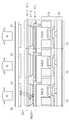
도 5는, 유기 EL 패널의 외관 구성 예를 나타낸다. 유기 EL 패널(11)은, 지지 기판(13)의 화소 어레이부의 형성 영역에 대향부(15)를 접착시킴으로써 얻은 구 조를 갖고 있다.5 shows an example of appearance configuration of an organic EL panel. The
지지 기판(13)은, 유리, 플라스틱, 또는 다른 재료로 구성되고, 그 표면에 유기 EL층이나 보호막 등을 형성한다. 대향부(15)의 베이스는, 유리, 플라스틱, 또는 다른 투명부재로 구성된다. 유기 EL 패널(11)에는, 외부로부터/에 지지 기판(13)에/으로부터 신호 등을 입출력하기 위한 FPC(flexible printed circuit)(17)이 배치된다.The
(B)제1 형태 예(B) Example 1
(B-1) 시스템 구성(B-1) System Configuration
이하에서는, N채널형의 박막 트랜지스터로 구성된 구동 트랜지스터 T2의 특성 변동을 막고, 또 화소 회로를 구성하는 소자 수가 적은 유기 EL 패널(11)의 시스템 구성 예를 나타낸다.Hereinafter, an example of the system configuration of the
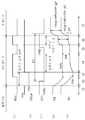
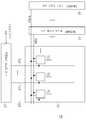
도 6은, 유기 EL 패널(11)의 시스템 구성 예다. 도 6에 나타내는 유기 EL 패널(11)은, 화소 어레이부(21)와, 화소 어레이부(21)의 구동회로로서의 기록제어선 구동부(23), 전류공급선 구동부(25), 수평 셀렉터(27), 및 타이밍 제너레이터(29)로 구성된다.6 is a system configuration example of the
화소 어레이부(21)는, 신호선 DTL과 기록제어선 WSL과의 각 교점 위치에 서브 화소를 배치한 매트릭스 구조를 갖고 있다. 서브 화소는 1화소를 구성하는 화소 구조의 최소 단위다. 예를 들면, 화이트 유닛(white unit)으로서의 1화소는, 유기 EL 재료가 서로 다른 3개의 서브 화소(R, G, B)로 구성된다.The
도 7은, 서브 화소에 대응하는 화소회로와 각 구동회로와의 접속 관계를 나 타낸다. 도 8은, 제1 형태 예로서 제안하는 화소회로의 내부구성을 나타낸다. 도 8에 나타내는 화소회로는, 2개의 N채널형의 박막 트랜지스터 T1 및 T2과 1개의 저장용량 Cs로 구성된다.7 shows a connection relationship between a pixel circuit corresponding to a sub pixel and each driving circuit. Fig. 8 shows the internal structure of the pixel circuit proposed as an example of the first embodiment. The pixel circuit shown in FIG. 8 is composed of two N-channel thin film transistors T1 and T2 and one storage capacitor Cs.
이 회로 구성에서도, 기록제어선 구동부(23)는, 기록제어선 WSL을 통해서 기록 트랜지스터 T1의 개폐를 제어하고, 그것에 의해 신호선 전위를 저장용량 Cs에 기록하는 것을 제어한다. 기록제어선 구동부(23)는, 수직 해상도와 같은 출력단 수를 갖는 시프트 레지스터로 구성된다.Also in this circuit configuration, the write
전류공급선 구동부(25)는, 구동 트랜지스터 T2의 한쪽의 주 전극에 접속되는 전류공급선 DSLa를 2치적으로 제어하고, 다른 구동회로와의 협동 동작에 의해 화소회로 내의 동작을 제어한다. 이 화소회로에서의 동작에는, 유기 EL 소자의 발광/비발광뿐만 아니라, 특성 변동의 보정동작도 포함된다. 이 형태 예의 경우, 특성 변동의 보정은, 구동 트랜지스터 T2의 임계치의 변동과 이동도의 변동에 의해 유니포미티(uniformity)의 열화의 보정을 의미한다.The current
수평 셀렉터(27)는, 신호선 DTL에 화소 데이터 Din에 의존한 신호전위 Vsig 또는 임계치 보정용의 오프셋 전위 Vofs를 인가한다. 또한, 수평 셀렉터(27)는, 수평 해상도와 같은 출력단 수를 갖는 시프트 레지스터와, 각 출력단에 대응하는 래치회로와, D/A 변환회로와, 버퍼 회로와, 셀렉터로 구성된다.The
타이밍 제너레이터(29)는, 기록제어선 WSL, 전류공급선 DSLa, 및 신호선 DTL의 구동에 필요한 타이밍 펄스를 생성한다.The
(B-2) 구동 동작 예(B-2) Drive operation example
도 9a 내지 9e는, 도 8에 나타내는 화소회로의 구동 동작 예를 나타낸다. 도 9a 내지 9e에서는, 전류공급선 DSLa에 인가하는 2종류의 전원전위 중, 고전위(발광 전위)를 Vcc로 나타내고, 저전위(비발광 전위)를 Vss로 나타낸다.9A to 9E show examples of the driving operation of the pixel circuit shown in FIG. 8. 9A to 9E, among the two kinds of power source potentials applied to the current supply line DSLa, the high potential (luminescence potential) is represented by Vcc and the low potential (non-luminescence potential) is represented by Vss.
우선, 발광 상태에 있어서의 화소회로 내의 동작 상태를 도 10에 나타낸다. 이 상태에서, 기록 트랜지스터 T1은 오프 상태에 있다. 한편, 구동 트랜지스터 T2는 포화 영역에서 동작하고, 게이트 ·소스간 전압 Vgs에 따라 정해지는 전류 Ids를 유기 EL 소자 OLED에 공급한다(도 9a 내지 9e(t1)).First, the operating state in the pixel circuit in the light emitting state is shown in FIG. In this state, the write transistor T1 is in the off state. On the other hand, the driving transistor T2 operates in the saturation region and supplies the current Ids determined in accordance with the gate-source voltage Vgs to the organic EL element OLED (Figs. 9A to 9E (t1)).
다음에, 비발광 상태의 동작 상태를 설명한다. 비발광 상태의 시작시에는, 전류공급선 DSLa의 전위가 고전위 Vcc으로부터 저전위 Vss로 전환한다(도 9a 내지 9e(t2)). 이때, 유기 EL 소자의 임계치 전압 Vthel이 Vss-Vcath(캐소드 전위) <Vthel이면 유기 EL 소자는 소등한다.Next, the operation state of the non-luminescing state will be described. At the start of the non-luminescing state, the potential of the current supply line DSLa is switched from the high potential Vcc to the low potential Vss (Figs. 9A to 9E (t2)). At this time, if the threshold voltage Vthel of the organic EL element is Vss-Vcath (cathode potential) <Vthel, the organic EL element is turned off.
구동 트랜지스터 T2의 소스 전위 Vs는, 전류공급선 DSLa의 전위와 같게 된다. 즉, 유기 EL 소자의 애노드 전극은 저전위 Vss로 충전된다. 도 11은, 기간 t2에 있어서의 화소회로 내의 동작 상태를 나타낸다. 도 11에 파선으로 나타나 있는 바와 같이, 이때, 저장용량 Cs에 저장된 전하는 전류공급선 DSLa으로 방전된다.The source potential Vs of the drive transistor T2 is equal to the potential of the current supply line DSLa. That is, the anode electrode of the organic EL element is charged with low potential Vss. 11 shows an operating state in the pixel circuit in the period t2. As shown by broken lines in FIG. 11, at this time, the charge stored in the storage capacitor Cs is discharged to the current supply line DSLa.
이후, 신호선 DTL의 전위가 임계치 보정용의 오프셋 전위 Vofs로 천이한 후에, 기록제어선 WSL이 고전위로 변화하면, 온 동작한 기록 트랜지스터 T1을 통해서 구동 트랜지스터 T2의 게이트 전위가 오프셋 전위 Vofs로 변화한다(도 9a 내지 9e(t3)).Then, after the potential of the signal line DTL transitions to the offset potential Vofs for threshold correction, when the write control line WSL changes to a high potential, the gate potential of the driving transistor T2 changes to the offset potential Vofs through the on-state write transistor T1 ( 9A-9E (t3).
도 12는, 이 기간 t3에 있어서의 화소회로 내의 동작 상태를 나타낸다. 이 기간 t3에서, 구동 트랜지스터 T2의 게이트·소스간 전압 Vgs는 Vofs-Vss로 주어진다. 이 전압은, 구동 트랜지스터 T2의 임계치 전압 Vth보다도 크게 설정된다. 이것은 Vofs-Vss>Vth의 관계를 만족하지 않으면 임계치 보정동작을 실행할 수 없기 때문이다.12 shows an operating state in the pixel circuit in this period t3. In this period t3, the gate-source voltage Vgs of the driving transistor T2 is given by Vofs-Vss. This voltage is set larger than the threshold voltage Vth of the drive transistor T2. This is because the threshold correction operation cannot be performed unless the relationship of Vofs-Vss> Vth is satisfied.
다음에, 전류공급선 DSLa의 전위가 다시 고전위 Vcc로 전환한다(도 9a 내지 9e(t4)). 전류공급선 DSLa의 전위가 고전위 Vcc로 변화함으로써, 유기 EL 소자 OLED의 애노드 전위 Vel이 구동 트랜지스터 T2의 소스 전위 Vs가 된다.Next, the potential of the current supply line DSLa is switched back to the high potential Vcc (Figs. 9A to 9E (t4)). As the potential of the current supply line DSLa changes to a high potential Vcc, the anode potential Vel of the organic EL element OLED becomes the source potential Vs of the driving transistor T2.
도 13은, 이 기간 t4에 있어서의 화소회로 내의 동작 상태를 나타낸다. 도 13에서는, 유기 EL 소자 OLED를 등가회로로 나타낸다. 즉, 다이오드와 기생 용량Cel로 나타낸다. 이 기간 t4에서, Vel≤Vcat+Vthel의 관계를 충족시키는 한(유기 EL 소자의 리이크 전류가 구동 트랜지스터 T2에 흐르는 구동전류 Ids보다 상당히 작다고 하는 가정에 근거해서), 구동 트랜지스터 T2에 흐르는 구동전류 Ids는, 저장용량 Cs와 기생 용량 Cel을 충전하는데도 사용된다.13 shows an operating state in the pixel circuit in this period t4. In FIG. 13, organic electroluminescent element OLED is shown by the equivalent circuit. That is, it is represented by a diode and a parasitic capacitance Cel. In this period t4, as long as the relationship of Vel≤Vcat + Vthel is satisfied (based on the assumption that the leakage current of the organic EL element is considerably smaller than the driving current Ids flowing in the driving transistor T2), the driving current flowing in the driving transistor T2. Ids is also used to charge the storage capacity Cs and the parasitic capacity Cel.
결과적으로, 유기 EL 소자 OLED의 애노드 전위 Vel은, 도 14에 나타나 있는 바와 같이, 시간의 경과와 함께 상승한다. 즉, 구동 트랜지스터 T2의 게이트 전위Vg은 오프셋 전위 Vofs로 고정한 상태 그대로, 구동 트랜지스터 T2의 소스 전위 Vs가 상승을 시작한다. 이 동작이 임계치 보정동작이다.As a result, the anode potential Vel of the organic EL element OLED rises with the passage of time, as shown in FIG. That is, the source potential Vs of the drive transistor T2 starts rising as the gate potential Vg of the drive transistor T2 is fixed at the offset potential Vofs. This operation is a threshold correction operation.
그러는 동안, 구동 트랜지스터 T2의 게이트·소스간 전압 Vgs는 임계치 전압Vth에 수속(收束)한다. 이때, Vel=Vofs-Vth≤Vcat+Vthel의 관계를 만족시키고 있다.In the meantime, the gate-source voltage Vgs of the drive transistor T2 converges on the threshold voltage Vth. At this time, the relationship of Vel = Vofs-Vth ≦ Vcat + Vthel is satisfied.
임계치 보정기간이 종료하면, 기록 트랜지스터 T1이 다시 오프된다(도 9a 내지 9e(t5)). When the threshold correction period ends, the write transistor T1 is turned off again (Figs. 9A to 9E (t5)).
이 오프에 의해, 구동 트랜지스터 T2의 게이트 전위 Vg은 플로팅 상태가 된다. 다만, 게이트·소스간 전압 Vgs는 임계치 전압 Vth에 수속하고 있으므로 구동 트랜지스터 T2는 컷오프 상태에 있어, 구동전류 Ids는 흐르지 않는다.By this off, the gate potential Vg of the drive transistor T2 is in a floating state. However, since the gate-source voltage Vgs converges to the threshold voltage Vth, the driving transistor T2 is in the cutoff state, and the driving current Ids does not flow.
이후, 신호선 DTL의 전위가 신호전위 Vsig로 천이하는데 필요한 타이밍 이후에, 기록 트랜지스터 T1은 다시 온 상태로 제어된다(도 9a 내지 9e(t6)). 도 15는, 이 기간 t6에 있어서의 화소회로 내의 동작 상태를 나타낸다. 신호전위 Vsig은, 대응화소의 계조값에 따라 공급되는 전위다.Thereafter, after the timing necessary for the potential of the signal line DTL to transition to the signal potential Vsig, the write transistor T1 is controlled to be in the on state again (Figs. 9A to 9E (t6)). 15 shows an operating state in the pixel circuit in this period t6. The signal potential Vsig is a potential supplied in accordance with the gradation value of the corresponding pixel.
이 기간 t6에서, 구동 트랜지스터 T2의 게이트 전위 Vg은, 신호전위 Vsig로 천이한다. 즉, 게이트·소스간 전압 Vgs가 임계치 전압 Vth보다 커진다. 이에 따라, 구동 트랜지스터 T2은 온 상태가 되어, 저장용량 Cs와 기생 용량 Cel을 충전하도록 구동전류 Ids를 흘려보내기 시작한다.In this period t6, the gate potential Vg of the driving transistor T2 transitions to the signal potential Vsig. That is, the gate-source voltage Vgs becomes larger than the threshold voltage Vth. As a result, the driving transistor T2 is turned on to start flowing the driving current Ids to charge the storage capacitor Cs and the parasitic capacitance Cel.
이 구동전류 Ids의 공급 시작에 따라, 구동 트랜지스터 T2의 소스 전위 Vs는 상승한다. 구동 트랜지스터 T2의 소스 전위 Vs가 유기 EL 소자의 임계치 전압 Vthel과 캐소드 전압 Vcat의 합을 초과하지 않는 한(유기 EL 소자 OLED에 흘러 들어 오는 리이크 전류가 구동전류 Ids보다도 상당히 작으면), 구동 트랜지스터 T2에 의해 공급되는 구동전류 Ids는, 저장용량 Cs와 기생 용량 Cel을 충전하는데 사용된다.As the supply current of the drive current Ids starts, the source potential Vs of the drive transistor T2 rises. As long as the source potential Vs of the driving transistor T2 does not exceed the sum of the threshold voltage Vthel and the cathode voltage Vcat of the organic EL element (when the leakage current flowing into the organic EL element OLED is considerably smaller than the driving current Ids), the driving transistor The drive current Ids supplied by T2 is used to charge the storage capacity Cs and the parasitic capacitance Cel.
이 동작 개시 시점에 있어서는, 이미 구동 트랜지스터 T2의 임계치 보정동작 이 완료했다. 따라서, 구동 트랜지스터 T2로부터 공급되는 구동전류 Ids는, 구동 트랜지스터 T2의 이동도 μ을 반영한 값이 된다. 구체적으로는, 구동 트랜지스터가 이동도 μ보다 크면, 보다 큰 구동전류 Ids가 흘러, 소스 전위 Vs의 상승도 한층 더 빨라진다.At the start of this operation, the threshold correction operation of the driving transistor T2 has already been completed. Therefore, the drive current Ids supplied from the drive transistor T2 becomes a value which reflects the mobility µ of the drive transistor T2. Specifically, when the driving transistor is larger than the mobility μ, a larger driving current Ids flows, and the rise of the source potential Vs becomes even faster.
반대로, 구동 트랜지스터가 보다 낮은 이동도 μ를 가지면, 보다 작은 구동전류 Ids가 흘러서, 소스 전위 Vs의 상승도 더 늦어진다(도 16).On the contrary, when the driving transistor has a lower mobility µ, smaller driving current Ids flows, resulting in a slower rise of the source potential Vs (Fig. 16).
결과적으로, 저장용량 Cs에 저장된 전압은, 구동 트랜지스터 T2의 이동도 μ 에 따라 보정된다. 즉, 구동 트랜지스터 T2의 게이트·소스간 전압 Vgs는, 이동도 μ을 보정한 전압으로 변화한다.As a result, the voltage stored in the storage capacitor Cs is corrected according to the mobility mu of the driving transistor T2. In other words, the gate-source voltage Vgs of the drive transistor T2 changes to the voltage at which the mobility µ is corrected.
최후에, 기록 트랜지스터 T1이 오프되어서, 신호전위 Vsig의 기록이 종료한다. 이때, 구동 트랜지스터 T2의 게이트·소스간 전압 Vgs(=Vsig-Vofs+Vth-ΔV)은, 임계치 전압 Vth보다 크다. 따라서, 구동전류 Ids'의 공급이 계속되고, 유기 EL 소자 OLED의 발광이 개시된다.Finally, the write transistor T1 is turned off, and the writing of the signal potential Vsig ends. At this time, the gate-source voltage Vgs (= Vsig-Vofs + Vth-ΔV) of the driving transistor T2 is larger than the threshold voltage Vth. Therefore, supply of drive current Ids' is continued, and light emission of organic electroluminescent element OLED is started.
유기 EL 소자 OLED에 구동전류 Ids'가 흐름으로써, 구동 트랜지스터 T2의 소스 전위 Vs는 전위 Vx까지 상승한다. 도 17은 이 발광 기간에 있어서의 화소회로 내의 동작 상태를 나타낸다.As the driving current Ids' flows to the organic EL element OLED, the source potential Vs of the driving transistor T2 rises to the potential Vx. 17 shows an operating state in the pixel circuit in this light emission period.
이 발광 기간에서, 구동 트랜지스터 T2의 게이트 전위 Vg는 플로팅 상태에 있다. 따라서, 구동 트랜지스터 T2의 게이트 전위 Vg은, 저장용량 Cs의 부트스트랩 동작에 의해, 게이트·소스간 전압 Vgs를 일정하게 유지한 채 상승한다(도 9a 내지 9e(t7)).In this light emission period, the gate potential Vg of the driving transistor T2 is in a floating state. Therefore, the gate potential Vg of the drive transistor T2 rises while maintaining the gate-source voltage Vgs constant by the bootstrap operation of the storage capacitor Cs (FIGS. 9A to 9E (t7)).
또한, 이 형태 예로서 제안하는 구동회로에서도, 총 발광 시간이 길어지면, 유기 EL 소자 OLED의 I-V 특성이 변화한다. 즉, 구동 트랜지스터 T2의 소스 전위 Vs도 변화한다.Also in the driving circuit proposed as an example of this embodiment, when the total light emission time becomes long, the I-V characteristics of the organic EL element OLED change. That is, the source potential Vs of the drive transistor T2 also changes.
그렇지만, 구동 트랜지스터 T2의 게이트·소스간 전압 Vgs는, 저장용량 Cs에 의해 일정하게 유지되므로 유기 EL 소자 OLED에 흐르는 전류량은 변화하지 않는다.However, since the gate-source voltage Vgs of the driving transistor T2 is kept constant by the storage capacitor Cs, the amount of current flowing through the organic EL element OLED does not change.
이 형태 예로서 제안하는 화소회로와 구동방식을 채용하면, 유기 EL 소자 OLED의 I-V 특성의 변화에 관계없이, 신호전위 Vsig에 의존한 구동전류 Ids를 항상 공급할 수 있다.By adopting the pixel circuit and the driving method proposed as an example of this embodiment, it is possible to always supply the driving current Ids depending on the signal potential Vsig regardless of the change in the I-V characteristic of the organic EL element OLED.
즉, 유기 EL 소자 OLED의 특성의 시간경과에 따른 변화에 관계없이, 발광 휘도를 신호전위 Vsig에 의존한 휘도로 계속해서 유지할 수 있다.That is, regardless of the change over time of the characteristics of the organic EL element OLED, the emission luminance can be continuously maintained at the luminance depending on the signal potential Vsig.
(B-3) 정리(B-3) Theorem
이상과 같이, 이 형태 예에서 설명한 화소회로와 구동방식의 채용에 의해, 구동 트랜지스터 T2을 N채널형의 박막 트랜지스터로 구성할 경우에도, 화소마다 휘도 변동이 없는 유기 EL 패널을 실현할 수 있다. 또한, N채널형의 박막 트랜지스터만을 이용해서 화소회로를 구성할 수 있어, 유기 EL 패널의 제조에 아모르포스(amorphous) 실리콘계의 프로세스를 채용하는 것이 가능하게 된다.As described above, by adopting the pixel circuit and the driving method described in this embodiment, even when the driving transistor T2 is formed of an N-channel thin film transistor, it is possible to realize an organic EL panel with no luminance variation for each pixel. In addition, the pixel circuit can be constructed using only the N-channel thin film transistor, and it becomes possible to employ an amorphous silicon-based process for the manufacture of the organic EL panel.
(C)제2 형태 예(C) Example 2
(C-1) 다른 기술과제의 고찰(C-1) Consideration of other technical tasks
전술한 바와 같이, 유기 EL 소자 OLED는 전류구동소자다. 이 때문에, 전류공급선 DSLa에는, 각 화소회로에 필요한 구동전류 Ids가 누적적으로 흐르고 있다. 도 18은, 전류공급선 DSLa가 수평 라인에 대하여 평행하게 연장될 경우에 있어서의 화소위치와 전압 강하와의 관계를 나타낸다. 도 18에서는, 전류공급선 DSLa의 저항성분을 명시적으로 나타내고 있다.As described above, the organic EL element OLED is a current driving element. For this reason, the drive current Ids required for each pixel circuit flows cumulatively in the current supply line DSLa. Fig. 18 shows the relationship between the pixel position and the voltage drop when the current supply line DSLa extends in parallel with the horizontal line. In Fig. 18, the resistance component of the current supply line DSLa is explicitly shown.
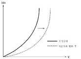
도 18에 나타낸 저항성분의 영향에 의해, 화소위치가 전류공급선 구동부(25)로부터 더 멀어짐에 따라 전류공급선 DSLa의 전압강하의 양이 서서히 커진다. 이것은, 1화소당의 전압강하를, 각 화소회로에 대응하는 구동전류 Ids와 1화소당의 배선 저항의 적으로서 나타내기 때문이다. 당연히, 화면의 우측에 위치하는 화소회로의 전원전위 Vy는, 화면의 좌측에 위치하는 화소회로의 전원전위 Vx보다도 낮다.Under the influence of the resistance component shown in FIG. 18, as the pixel position is further from the current
이 전원전위의 저하는, 화소회로를 구성하는 구동 트랜지스터 T2의 드레인·소스간 전압 Vds를 작게 하는 작용을 한다.This drop in power supply potential serves to reduce the drain-source voltage Vds of the driving transistor T2 constituting the pixel circuit.
도 19는, 화면의 우측단과 좌측단의 전원전위의 차가 구동전류 Ids에 주는 영향을 나타낸다. 도 19에 나타나 있는 바와 같이, 같은 계조값에서도, 구동전류Ids가 다르면, 발광 휘도차가 발생한다. 이 현상은 쉐이딩 현상으로서 지각된다.Fig. 19 shows the effect of the difference in power supply potential between the right and left ends of the screen on the drive current Ids. As shown in Fig. 19, even in the same gradation value, if the driving current Ids is different, the light emission luminance difference occurs. This phenomenon is perceived as a shading phenomenon.
이 쉐이딩이라고 불리는 현상은, 전술한 바와 같이 전류공급선 DSLa의 배선구조에 기인한다. 이 때문에, 제1 형태 예에서 설명한 구동 트랜지스터 T2의 특성보정 기능에서는, 그 쉐이딩 발생을 막는 것은 불가능하다.This phenomenon called shading is due to the wiring structure of the current supply line DSLa as described above. For this reason, in the characteristic correction function of the driving transistor T2 described in the first embodiment, it is impossible to prevent the shading.
게다가, 쉐이딩 현상은, 크로스토크(crosstalk)의 발생에도 관련이 있다.In addition, the shading phenomenon is also related to the occurrence of crosstalk.
크로스토크란, 도 20a에 나타나 있는 바와 같은 화상(모든 백색 배경 화상의 일부 영역에 흑색 표시창을 배치한 화상 등)의 표시시에, 도 20b에 나타나 있는 바와 같이 수평 라인 간에서 휘도차가 지각되는 현상을 말한다. 구체적으로는, 흑색 표시창과 같은 수평 라인의 배경 흰색 부분과, 흑색 표시창의 상하에 위치하는 수평 라인의 배경 흰색 부분과의 사이에 휘도차가 생기는 현상을 말한다.Crosstalk is a phenomenon in which a luminance difference is perceived between horizontal lines as shown in FIG. 20B when displaying an image as shown in FIG. 20A (such as an image in which black display windows are arranged in a partial region of all white background images). Say Specifically, a phenomenon in which a luminance difference occurs between a background white portion of a horizontal line such as a black display window and a background white portion of a horizontal line positioned above and below the black display window is described.
이 휘도차는, 도 21에 나타나 있는 바와 같이 흑색 표시창 부분에 대응하는 화소회로에는 구동전류 Ids가 흐르지 않는 상태에 영향을 주고 있다. 구체적으로는, 이 휘도차는 흑색 표시창 부분에서의 전류공급선 DSL의 전압강하가 매우 작은 상태에 영향을 주고 있다. 결과적으로, 흑색 표시창 부분과 같은 열의 화면 우측단 부근에 있어서의 전류공급선 DSL의 전압강하는 매우 작아, 높은 발광 휘도가 얻어진다.This luminance difference affects a state in which the driving current Ids does not flow in the pixel circuit corresponding to the black display window portion as shown in FIG. Specifically, this luminance difference affects a state where the voltage drop of the current supply line DSL in the black display window portion is very small. As a result, the voltage drop of the current supply line DSL near the right end of the screen in the same column as the black display window portion is very small, and high light emission luminance is obtained.
한편, 도 21에 나타나 있는 바와 같이 흑색 표시창과는 다른 수평라인 상의 화면 우측단 부근에서는, 전압강하의 누적에 의해 전압강하량이 커진다. 즉, 발광 휘도는 전원전위의 강하만큼 낮아진다. 결과적으로, 같은 화면 우측단의 열에서도, 흑색 표시창이 있는 수평 라인과 그 밖의 수평 라인과의 사이에서는 휘도차가 발생하고, 그 휘도차가 일정량 이상이 되면 시각적으로 인식된다.On the other hand, as shown in Fig. 21, in the vicinity of the right end of the screen on a horizontal line different from the black display window, the voltage drop amount increases due to the accumulation of the voltage drop. That is, the light emission luminance is lowered by the drop of the power potential. As a result, even in the column on the right side of the same screen, a luminance difference is generated between the horizontal line with the black display window and the other horizontal line, and visually recognized when the luminance difference becomes a certain amount or more.
전압강하량은, 구동전류와 전류공급선의 배선 저항과의 곱의 합으로서 취득된다.The voltage drop amount is obtained as the sum of the product of the drive current and the wiring resistance of the current supply line.
예를 들면, 도 21의 패널구조의 경우, 수평라인 상의 화소수(R화소, G화소, B화소의 모두를 포함한다)를 N, 각 화소에서 필요로 하는 구동전류 Ids의 최대값을 I, 1화소당의 배선 저항을 r이라고 하면, 전류공급선 DSL 중 전류공급선 구동부(25)로부터 가장 먼 위치(이 형태 예의 경우, 화면 우측단)의 전원강하량 Vy는, 다음 식으로 주어진다.For example, in the case of the panel structure of Fig. 21, the number of pixels (including all of the R pixels, the G pixels, and the B pixels) on the horizontal line is N, and the maximum value of the driving current Ids required for each pixel is I, If the wiring resistance per pixel is r, the power supply drop amount Vy at the position furthest from the current
Vy = {N(N+1)/2}×I×r (식1)Vy = {N (N + 1) / 2} × I × r (Equation 1)
따라서, 전압강하량을 작게 하기 위해서는, N, I, r의 적어도 하나를 작게 하면 된다.Therefore, in order to reduce the voltage drop amount, at least one of N, I, and r may be reduced.
여기에서는, 배선 저항 r를 작게 하는 것을 고려한다. 배선 저항 r를 작게 하기 위해서는, 전류공급선 DSL의 배선 폭을 증가시키거나, 전류공급선 DSL을 구성하는 금속막(예를 들면, 알루미늄막)의 두께를 증가시키는 것이 필요하다.Here, consideration is given to reducing the wiring resistance r. In order to reduce the wiring resistance r, it is necessary to increase the wiring width of the current supply line DSL or increase the thickness of the metal film (for example, the aluminum film) constituting the current supply line DSL.
이들 방법 중, 막 두께를 증대하는 방법은 프로세스의 변경을 수반하고, 생산 택트(takt)나 수율의 저하 등을 초래할 가능성이 있다. 이 때문에, 다른 방법이 선택되어야 한다. 즉, 전류공급선 DSL의 선폭을 증가시키는 방법이 선택되어야 한다.Among these methods, the method of increasing the film thickness is accompanied by a change in the process, which may cause a production tact, a decrease in yield, and the like. Because of this, another method must be chosen. That is, a method of increasing the line width of the current supply line DSL should be selected.
도 22는, 제1 형태 예에 대응하는 화소회로(31)의 배치 예를 나타낸다. 도 8과 같은 도 22의 부호는, 같은 구성소자를 나타낸다. 도 22의 경우, 전류공급선 DSLa의 선폭은 W1로 나타낸다.22 shows an example of arrangement of
도 23은, 전류공급선 DSLa의 선폭을 W2(>W1)까지 증가시킨 배치 예를 나타낸다. 도 23의 배치를 채용하면, 전류공급선 DSLa의 배선 저항을 작게 할 수 있다. 결과적으로, 쉐이딩 및 크로스토크의 개선을 기대할 수 있다.Fig. 23 shows an arrangement example in which the line width of the current supply line DSLa is increased to W2 (> W1). By adopting the arrangement shown in Fig. 23, the wiring resistance of the current supply line DSLa can be reduced. As a result, improvement in shading and crosstalk can be expected.
그렇지만, 전류공급선 DSLa의 선폭이 증가하면, 전류공급선 DSLa와 신호선 DTL이 교차하는 부분(도 23에서 파선으로 둘러싸여 나타낸 부호 A의 부분)의 면적이 증가한다.However, if the line width of the current supply line DSLa is increased, the area of the portion where the current supply line DSLa and the signal line DTL intersect (part of symbol A shown surrounded by broken lines in FIG. 23) increases.
이 면적의 증가는, 전류공급선 DSLa와 신호선 DTL과의 사이에 형성되는 배선 간 용량(커플링 용량)의 증가를 의미한다. 즉, 면적의 증가에 의해 전류공급선 DSLa의 전위 변동이 신호선 DTL에 전파하기 쉬워지는 또 다른 기술과제가 발생한다.An increase in this area means an increase in the inter-wire capacitance (coupling capacitance) formed between the current supply line DSLa and the signal line DTL. That is, another technical problem arises in that the potential variation of the current supply line DSLa is easily propagated to the signal line DTL due to the increase in the area.
예를 들면, 어떤 수평 라인에 대응하는 화소회로의 신호전위 Vsig의 기록 타이밍에서, 또 다른 수평 라인에 대응하는 전류공급선 DSLa의 전위가 변동할 가능성이 있다. 이 경우, 이동도 보정기간 중에 전류공급선 DSLa의 전위의 변동에 의한 구동 트랜지스터 T2의 게이트와 소스의 전위 변동이 캔슬되지 않으면, 구동 트랜지스터 T2의 이동도 보정이 부정확하게 실행될 것이다.For example, at the timing of writing the signal potential Vsig of the pixel circuit corresponding to a certain horizontal line, the potential of the current supply line DSLa corresponding to another horizontal line may change. In this case, if the potential variation of the gate and the source of the driving transistor T2 due to the variation of the potential of the current supply line DSLa is not canceled during the mobility correction period, the mobility correction of the driving transistor T2 will be executed incorrectly.
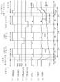
도 24a 내지 24f는, 어떤 수평 라인에 대응하는 화소회로(31)의 구동 동작 예를 나타낸다. 주목하는 수평 라인의 위치를 첨자 "i"로 나타낸다. 첨자 "i"는, 화면의 가장 위쪽의 행으로부터 i번째에 위치하는 수평 라인을 의미한다.24A to 24F show examples of the driving operation of the
도 24a는, i번째의 수평 라인에 대응하는 화소회로(31)의 기록제어선 WSL(i)의 신호 파형 예다. 도 24b는, i번째의 수평 라인에 대응하는 전류공급선 DSLa(i)의 신호 파형 예다. 도 24c는, i+1번째의 수평 라인에 대응하는 전류공급선 DSLa(i+1)의 신호 파형 예다.24A is an example of signal waveforms of the write control line WSL (i) of the
도 24d는, 전류공급선과 교차하는 신호선 DTL의 신호 파형을 나타낸다. 도 24e는, i번째의 수평 라인에 대응하는 화소회로(31)를 구성하는 구동 트랜지스터 T2의 게이트 전위 Vg의 신호 파형이다. 도 24f는, i번째의 수평 라인에 대응하는 화소회로(31)를 구성하는 구동 트랜지스터 T2의 소스 전위 Vs의 신호 파형이다.24D shows the signal waveform of the signal line DTL intersecting with the current supply line. 24E is a signal waveform of the gate potential Vg of the driving transistor T2 constituting the
도 24d에 나타나 있는 바와 같이, 전류공급선 DSLa의 전위변동은, 이 전위변 동이 이동도 보정 대상으로서의 화소회로와 같은 행에서 발생했는지 혹은 또 다른 행에서 발생했는지의 여부에 관계없이 교차부분의 배선 용량을 통해서 신호선 DTL(i)에 전파된다. 도 24a 내지 24f의 경우, 신호전위 Vsig의 기록 및 이동도 보정 기간 중(t6)에 있어서의 전원전위의 변동(고전위 Vcc로부터 저전위 Vss로의 변동)이 구동 트랜지스터 T2의 게이트 전위 Vg와 소스 전위 Vs에 미치는 현상을 확인할 수 있다.As shown in Fig. 24D, the potential variation of the current supply line DSLa is equal to the wiring capacitance at the intersection portion regardless of whether the potential variation occurs in the same row or another row as the pixel circuit as the mobility correction target. It propagates to the signal line DTL (i) through. In the case of FIGS. 24A to 24F, the fluctuation of the power supply potential (the fluctuation from the high potential Vcc to the low potential Vss) during the recording and mobility correction period (t6) of the signal potential Vsig changes the gate potential Vg and the source potential of the driving transistor T2. The phenomenon affecting Vs can be confirmed.
그럼에도 불구하고, 게이트 전위 Vg와 소스 전위 Vs가 이동도 보정기간 중에 본래의 전위로 돌아가면, 문제없이 이동도 보정동작을 완료할 수 있다. 그러나, 이들 전위가 본래의 전위로 돌아가지 않을 경우, 이동도 보정동작을 정상적으로 완료할 수 없다.Nevertheless, if the gate potential Vg and the source potential Vs return to their original potentials during the mobility correction period, the mobility correction operation can be completed without any problem. However, if these potentials do not return to their original potentials, the mobility correction operation cannot be completed normally.
그 이유는, 소스 전위 Vs의 전위변동량은, 저장용량 Cs를 매개로 인해 게이트 전위 Vg의 전위변동량보다 작기 때문이다.This is because the potential variation in the source potential Vs is smaller than the potential variation in the gate potential Vg through the storage capacitor Cs.
즉, 게이트 전위 Vg의 변동이 이동도 보정기간 중에 캔슬되지 않으면, 정상적인 이동도 보정의 경우에 비해서 구동 트랜지스터 T2의 게이트·소스간 전압 Vgs가 작아진다. 이것은, 화면상의 휘도가 본래의 휘도 레벨보다도 낮아지는 것을 의미한다.In other words, if the fluctuation of the gate potential Vg is not canceled during the mobility correction period, the gate-source voltage Vgs of the driving transistor T2 becomes smaller than in the case of normal mobility correction. This means that the brightness on the screen is lower than the original brightness level.
게다가, 커플링의 영향에 의한 전위의 변동량은, 신호전위 Vsig와는 무관하게 일정하다.In addition, the amount of change in potential due to the influence of the coupling is constant regardless of the signal potential Vsig.
따라서, 신호전위 Vsig가 저휘도의 값을 갖는 경우, 이 휘도 레벨의 저하는 더욱 크게 나타나게 된다. 이것은, 100% 흑색으로서의 낮아지는 측의 그레이스케 일(grayscale)의 잘못된 표현 및 감마 보정의 부족으로서 화질의 저하를 일으킨다.Therefore, when the signal potential Vsig has a value of low luminance, the decrease in this luminance level appears more evenly. This causes a deterioration in image quality due to the incorrect representation of grayscale on the lower side as 100% black and the lack of gamma correction.
또한, 이 신호선 DTL에의 전위변동의 전파는, 임계치 보정기간이 복수의 수평주사기간에서 복수의 기간으로 분할될 경우에 화소회로의 구동에 영향을 주는 경우가 있다.Further, the propagation of the potential variation to the signal line DTL may affect the driving of the pixel circuit when the threshold correction period is divided into a plurality of horizontal scanning periods.
예를 들면, 어떤 수평 라인에 대응하는 화소회로의 임계치 보정기간 중에, 다른 수평 라인에 대응하는 전류공급선 DSLa의 전위가 변동할 가능성이 있다. 이 경우, 임계치 보정기간 중에 전류공급선 DSLa의 전위의 변동에 의한 구동 트랜지스터 T2의 게이트와 소스의 전위 변동이 캔슬되지 않으면, 구동 트랜지스터 T2의 임계치 보정이 정확하게 실행되지 않는다.For example, during the threshold correction period of the pixel circuit corresponding to one horizontal line, there is a possibility that the potential of the current supply line DSLa corresponding to the other horizontal line is changed. In this case, if the potential variation of the gate and the source of the driving transistor T2 due to the variation of the potential of the current supply line DSLa is not canceled during the threshold correction period, the threshold correction of the driving transistor T2 is not executed correctly.
도 25a 내지 25g는, 어떤 수평 라인에 대응하는 화소회로(31)의 구동 동작 예를 나타낸다. 특히, 도 25a 내지 25g는, 임계치 보정동작을 3수평 주사 기간으로 분할해서 실행하는 경우의 동작 예다. 또한, 도 25a 내지 25g에 있어서도, 주목하는 수평 라인의 위치를 첨자 "i"로 나타낸다. 첨자 "i"는, 화면의 가장 위에 있는 행으로부터 i번째의 행에 위치하는 수평 라인을 의미한다.25A to 25G show examples of the driving operation of the
도 25a는, i번째의 수평 라인에 대응하는 화소회로(31)의 기록제어선 WSL(i)의 신호 파형 예다. 도 25b는, i번째의 수평 라인에 대응하는 전류공급선 DSLa(i)의 신호 파형 예다. 도 25c는, i+1번째의 수평 라인에 대응하는 전류공급선 DSLa(i+1)의 신호 파형 예다.25A is an example of the signal waveform of the write control line WSL (i) of the
도 25d는, i+2번째의 수평 라인에 대응하는 전류공급선 DSLa(i+2)의 신호 파형 예다.25D is an example of signal waveforms of the current supply line DSLa (i + 2) corresponding to the i + 2th horizontal line.
도 25e는, 전류공급선과 교차하는 신호선 DTL의 신호 파형을 나타낸다. 도 25f는, i번째의 수평 라인에 대응하는 화소회로(31)를 구성하는 구동 트랜지스터 T2의 게이트 전위 Vg의 신호 파형이다. 도 25g는, i번째의 수평 라인에 대응하는 화소회로(31)를 구성하는 구동 트랜지스터 T2의 소스 전위 Vs의 신호 파형이다.25E shows the signal waveform of the signal line DTL intersecting with the current supply line. 25F is a signal waveform of the gate potential Vg of the driving transistor T2 constituting the
도 25e에 나타나 있는 바와 같이, 전류공급선 DSLa의 전위변동은, 이 전위변동이 임계치 보정 대상으로서의 화소회로와 같은 행에서 발생했는지 혹은 다른 행에서 발생했는지의 여부에 관계없이, 교차 부분의 배선 용량을 통해서 신호선 DTL에 전파된다. 도 25a 내지 25g의 경우, 기록 트랜지스터 T1이 온 상태인 기간 t3, t4, t6, t8의 전원전위의 변동(저전위 Vss로부터 고전위 Vcc로의 변동)이 구동 트랜지스터 T2의 게이트 전위 Vg와 소스 전위 Vs로 전파된다.As shown in Fig. 25E, the potential variation of the current supply line DSLa is obtained by varying the wiring capacitance of the intersection portion regardless of whether the potential variation occurs in the same row or in another row as the pixel circuit as the threshold correction target. It propagates through the signal line DTL. 25A to 25G, fluctuations in the power supply potential (change from low potential Vss to high potential Vcc) during the periods t3, t4, t6, and t8 in which the write transistor T1 is in the on state are the gate potential Vg and the source potential Vs of the driving transistor T2. Is propagated to.
이 경우에도, 게이트 전위 Vg와 소스 전위 Vs의 전위변동이 임계치 보정기간 중에 캔슬되면, 문제없이 임계치 보정을 완료할 수 있다. 그러나, 임계치 보정동작의 거의 종료 직전에 다른 행의 전류공급선 DSLa의 전위변동이 전파되어, 게이트 전위 Vg와 소스 전위 Vs가 변동해서 본래의 전위로 돌아가지 않는 경우에는, 임계치 보정동작을 정상적으로 완료할 수 없다.Even in this case, if the potential variation of the gate potential Vg and the source potential Vs is canceled during the threshold correction period, the threshold correction can be completed without any problem. However, if the potential variation of the current supply line DSLa in another row propagates almost immediately before the threshold correction operation is completed, and the gate potential Vg and the source potential Vs fluctuate and do not return to the original potential, the threshold correction operation is normally completed. Can't.
도 26a 내지 26d는, 그 이유를 나타낸다. 도 26a는, 전류공급선 DSLa에 전위변동이 생기기 전의 화소회로 내의 전위관계를 나타내고 있다. 도 26a의 경우, 구동 트랜지스터 T2의 게이트·소스간 전압 Vgs는 이미 임계치 전압 Vth에 수속되었다. 도 26b는, 임계치 보정기간의 종료 직전에 전류공급선 DSLa의 전위가 변동한 상태를 나타내고 있다.26A to 26D show the reason. Fig. 26A shows the potential relationship in the pixel circuit before the potential variation occurs in the current supply line DSLa. In the case of FIG. 26A, the gate-source voltage Vgs of the drive transistor T2 has already converged to the threshold voltage Vth. Fig. 26B shows a state in which the potential of the current supply line DSLa fluctuates immediately before the end of the threshold correction period.
이 시점의 게이트 전위 Vg는, 오프셋 전위 Vofs보다 전위 변동에 대응하는 ΔV만큼 크다. 한편, 소스 전위 Vs의 변동량 ΔVs는, 저장용량 Cs를 통해서 전위 변동이 전파되므로, 게이트 전위 Vg의 변동량 ΔV보다 작다. 이 때문에, 구동 트랜지스터 T2의 게이트·소스간 전압 Vgs는 임계치 전압 Vth보다 커지고, 구동 트랜지스터 T2은 다시 온한다.The gate potential Vg at this point is larger than the offset potential Vofs by ΔV corresponding to the potential variation. On the other hand, since the potential variation propagates through the storage capacitor Cs, the variation amount ΔVs of the source potential Vs is smaller than the variation amount ΔV of the gate potential Vg. For this reason, the gate-source voltage Vgs of the drive transistor T2 becomes larger than the threshold voltage Vth, and the drive transistor T2 turns on again.
결과적으로, 도 26c에 나타나 있는 바와 같이, 구동 트랜지스터 T2의 이동도 보정동작은 계속하므로, 소스 전위 Vs는 더욱더 ΔVs'만큼 상승한다.As a result, as shown in FIG. 26C, since the mobility correction operation of the driving transistor T2 continues, the source potential Vs further increases by ΔVs'.
드디어, 도 26d에 나타나 있는 바와 같이, 전류공급선 DSLa의 전위변동의 영향이 사라지면, 구동 트랜지스터 T2의 게이트 전위 Vg은 오프셋 전위 Vofs에 수속하고, 소스 전위 Vs는 전위변동 전의 전위보다 ΔVs'만큼 큰 전위에 수속한다.Finally, as shown in FIG. 26D, when the influence of the potential variation of the current supply line DSLa disappears, the gate potential Vg of the driving transistor T2 converges to the offset potential Vofs, and the source potential Vs is ΔVs' which is larger than the potential before the potential variation. Procedure to
이것은, 임계치 보정기간의 종료시점에서, 구동 트랜지스터 T2의 게이트·소스간 전압 Vgs가 임계치 전압 Vth보다도 낮은 전압 Vgs'으로 변화되었다는 것을 의미한다.This means that at the end of the threshold correction period, the gate-source voltage Vgs of the drive transistor T2 is changed to a voltage Vgs' which is lower than the threshold voltage Vth.
즉, 임계치 보정동작이 정상적으로 실행되지 않고 있는 것을 의미한다. 결과적으로, 발광 휘도가 본래의 휘도와 일치하지 않게 된다.In other words, it means that the threshold correction operation is not normally executed. As a result, the luminescence brightness does not match the original brightness.
또한, 전류공급선 DSLa와 신호선 DTL의 교차 면적의 증대는, 금속층끼리의 중첩 면적의 증대를 의미한다. 따라서, 교차 면적의 증대는, 층간 쇼트의 가능성을 향상시키는 원인으로도 된다.In addition, an increase in the cross-sectional area of the current supply line DSLa and the signal line DTL means an increase in the overlapping area between the metal layers. Therefore, the increase of the crossing area may be a cause for improving the possibility of the interlayer short.
또한, 도 23에 나타나 있는 바와 같이, 전류공급선 DSLa가 신호선 DTL의 상층(제2층)으로서 형성될 경우, 신호선 DTL 중 전류공급선 DSLa의 하층(제1층)부분 의 배선 길이가 길어진다. 이 경우에, 하층(제1층)부분의 배선 저항이 상층(제2층)의 배선 저항보다 크면, 신호선 DTL의 전체로서의 배선 저항이 커지는 원인으로도 된다.As shown in Fig. 23, when the current supply line DSLa is formed as an upper layer (second layer) of the signal line DTL, the wiring length of the lower layer (first layer) portion of the current supply line DSLa in the signal line DTL becomes long. In this case, if the wiring resistance of the lower layer (first layer) portion is larger than the wiring resistance of the upper layer (second layer), the wiring resistance as a whole of the signal line DTL may be increased.
(C-2) 제안하는 배치(C-2) Suggested Deployment
이들 문제를 해결하기 위해서, 본 발명자 등은, 도 27에 나타내는 배치를 제안한다. 즉, 전류공급선 DSLb 중 신호선 DTL과의 교차 부분만 작은 선폭 W3(<W 1)을 갖고, 전류공급선 DSLb의 그 밖의 부분은 큰 선폭 W4(>W1)을 갖는다.In order to solve these problems, the present inventors propose the arrangement shown in FIG. 27. That is, only the intersection portion of the current supply line DSLb with the signal line DTL has a small line width W3 (<W1), and the other portion of the current supply line DSLb has a large line width W4 (> W1).
이 때문에, 전류공급선 DSLb의 작은 선폭과 큰 선폭은, 수평 라인을 따라 화소 피치의 사이클로 교대로 출현하게 된다.For this reason, the small line width and large line width of the current supply line DSLb alternately appear in cycles of the pixel pitch along the horizontal line.
도 27의 경우, 전류공급선 DSL의 선폭은, 선폭 W3으로부터 선폭 W4로 서서히 수평방향을 따라 증가하고, 선폭 W4로부터 선폭 W3으로 서서히 수평방향을 따라 감소한다.In the case of Fig. 27, the line width of the current supply line DSL gradually increases along the horizontal direction from the line width W3 to the line width W4 and gradually decreases along the horizontal direction from the line width W4 to the line width W3.
무엇보다, 전류공급선 DSL의 선폭은, 선폭 W3과 W4의 사이에서 계단형(직각)으로 변화해도 된다.First of all, the line width of the current supply line DSL may change stepwise (right angle) between the line widths W3 and W4.
이 배선구조의 채용에 의해, 전류공급선 DSL의 전체로서의 배선 저항을 저하시킬 수 있어, 쉐이딩 및 크로스토크의 발생을 효과적으로 억제할 수 있다.By adopting this wiring structure, wiring resistance as a whole of the current supply line DSL can be reduced, and generation of shading and crosstalk can be effectively suppressed.
물론, 선폭 W3 및 W4(특히, W4)은, 식 1로 주어지는 전압강하량 Vy가 크로스토크의 시각적 인식과 관련된 한계값 미만으로 되도록 설계된다. 크로스토크의 시각적 인식과 관련된 한계값은, 사용 환경이나 수평주사 주기 등에 따라 다르다. 여기에서는, 한계값의 하나로서, 예를 들면, 가장 높은 계조값에 대응하는 휘도의 1% 가 이용가능하다.Of course, the line widths W3 and W4 (in particular, W4) are designed such that the voltage drop amount Vy given by
또한, 도 27에 나타낸 배선구조는, 전술한 그 밖의 과제도 해결할 수 있다.Further, the wiring structure shown in FIG. 27 can also solve other problems described above.
우선, 도 27에 나타낸 배선구조의 경우, 전류공급선 DSL과 신호선 DTL과의 사이에 형성되는 배선간 용량은 작다. 그 이유는, 배선부분의 선폭이 W3로 감소하기 때문이다. 이 때문에, 전류공급선 DSLb의 전위변동의 신호선 DTL에의 전파를 줄일 수 있다.First, in the case of the wiring structure shown in Fig. 27, the inter-wire capacitance formed between the current supply line DSL and the signal line DTL is small. This is because the line width of the wiring portion is reduced to W3. For this reason, the electric wave propagation to the signal line DTL of the potential change of the current supply line DSLb can be reduced.
따라서, 어떤 수평 라인에 대응하는 화소회로의 신호전위 Vsig의 기록 타이밍에서, 다른 수평 라인에 대응하는 전류공급선 DSLb의 전위가 변동하여, 기록 중의 신호전위 Vsig에 전위변동이 생긴 경우에도, 변동 자체가 작으므로 이동도 보정기간 중에 전위의 변동을 캔슬할 수 있다. 즉, 정상적인 이동도 보정의 실행을 확보할 수 있다.Therefore, even when the potential of the current supply line DSLb corresponding to another horizontal line changes at the timing of writing the signal potential Vsig of the pixel circuit corresponding to a certain horizontal line, even if the potential change occurs in the signal potential Vsig during recording, the variation itself is Since it is small, it is possible to cancel the fluctuation of the electric potential during the mobility correction period. In other words, execution of the normal mobility correction can be ensured.
도 28a 내지 28f는, 어떤 수평 라인에 대응하는 화소회로(31)의 구동 동작 예를 나타낸다. 도 28a 내지 28f는, 전술한 도 24a 내지 24f에 대응하는 도면이며, 주목하는 수평 라인의 위치를 첨자 "i"로 나타낸다. 따라서, 도 28a∼도 28f의 신호 파형은, 모두 도 24a∼도 24f의 신호 파형에 대응한다.28A to 28F show examples of the driving operation of the
물론, 본 발명자들이 제안하는 배선구조의 경우에도, 도 28d에 나타나 있는 바와 같이, 전류공급선 DSLb의 전위 변동이, 신호선 DTL과의 교차부분에 형성되는 배선간 용량을 통해서 신호선 DTL에 전파된다. 다만, 그 전파량은 도 24a 내지 24f보다 작다.Of course, even in the case of the wiring structure proposed by the present inventors, as shown in Fig. 28D, the potential variation of the current supply line DSLb is propagated to the signal line DTL through the inter-wire capacitance formed at the intersection with the signal line DTL. However, the propagation amount is smaller than those in Figs. 24A to 24F.
따라서, 신호전위 Vsig의 기록 및 이동도 보정기간 중(t6)에, 전원전위가 고전위 Vcc로부터 저전위 Vss로 변화될 때에도, 구동 트랜지스터 T2의 게이트 전위Vg과 소스 전위 Vs에 출현하는 변동량은 적다. Therefore, even when the power supply potential is changed from the high potential Vcc to the low potential Vss during the recording and mobility correction period t6 of the signal potential Vsig, the amount of variation that appears in the gate potential Vg and the source potential Vs of the driving transistor T2 is small. .
이 때문에, 게이트 전위 Vg와 소스 전위 Vs은, 거의 틀림없이 이동도 보정기간 중에 본래의 전위로 되돌리는 것이 가능해지므로, 이동도 보정동작을 기간 내에 완료할 수 있다. 따라서, 신호전위 Vsig가 고휘도의 값을 갖는 경우는 물론, 저휘도의 값을 갖는 경우에도, 계조값에 대응하는 본래의 발광 휘도를 실현할 수 있다.For this reason, the gate potential Vg and the source potential Vs are almost certainly able to return to the original potential during the mobility correction period, so that the mobility correction operation can be completed within the period. Therefore, even when the signal potential Vsig has a high luminance value as well as a low luminance value, the original light emission luminance corresponding to the gray scale value can be realized.
또한, 신호선 DTL에 전파된 전위 변동량의 억제는, 임계치 보정기간이 복수의 수평주사기간에서 복수의 기간으로 분할되는 경우에도 유리한 효과를 발휘한다.In addition, suppression of the amount of electric potential fluctuation propagated to the signal line DTL has an advantageous effect even when the threshold correction period is divided into a plurality of periods in a plurality of horizontal scanning periods.
여기에서는, 도 29a 내지 29g를 참조해서 이 특징을 설명한다. 도 29a 내지 29g는, 전술한 도 25a 내지 25g에 대응하는 도면이며, 주목하는 수평 라인의 위치를 첨자 "i"로 나타내고 있다. 따라서, 도 29a 내지 29g의 신호 파형은, 모두 도 25a∼도 25g의 신호 파형에 대응한다.Here, this characteristic is demonstrated with reference to FIGS. 29A-29G. 29A to 29G are views corresponding to the above-described Figs. 25A to 25G, and the positions of the horizontal lines of interest are indicated by the subscript "i". Therefore, the signal waveforms of Figs. 29A to 29G all correspond to the signal waveforms of Figs. 25A to 25G.
도 29a 내지 29g의 경우에도, 기록 트랜지스터 T1이 온 상태인 기간 t3, t4, t6, t8에 발생한 전류공급선 DSLb의 전위변동(저전위 Vss로부터 고전위 Vcc로의 변동)이, 구동 트랜지스터 T2의 게이트 전위 Vg와 소스 전위 Vs에 전파된다.Also in FIGS. 29A to 29G, the potential change (change from low potential Vss to high potential Vcc) of the current supply line DSLb generated in the periods t3, t4, t6, and t8 in which the write transistor T1 is in the on state is the gate potential of the driving transistor T2. Propagates to Vg and source potential Vs.
그렇지만, 본 발명자들이 제안하는 배선구조에 근거해 전류공급선 DSL과 신호선 DTL과의 교차 부분에 형성되는 배선간 용량(커플링 용량)은 작기 때문에, 전위변동의 전파량이 대단히 작다.However, based on the wiring structure proposed by the present inventors, since the inter-wiring capacitance (coupling capacitance) formed at the intersection of the current supply line DSL and the signal line DTL is small, the propagation amount of the potential variation is very small.
결과적으로, 게이트 전위 Vg와 소스 전위Vs의 전위변동이 임계치 보정기간의 종료 직전에 발생해도, 그 변동을 나머지의 보정기간 동안에 캔슬할 수 있으므로, 문제없이 임계치 보정을 완료할 수 있다. 또한, 임계치 보정동작의 완료 후에 전위변동이 전파되어 임계치 보정동작이 재개되어도, 그때에 나타나는 소스 전위 Vs의 상승량 ΔVs'은 무시할 수 있을 만큼 매우 작다. 따라서, 임계치 보정동작에의 영향을 고려할 필요가 없다.As a result, even if the potential variation of the gate potential Vg and the source potential Vs occurs immediately before the end of the threshold correction period, the variation can be canceled during the remaining correction period, so that the threshold correction can be completed without any problem. In addition, even if the potential variation propagates after the completion of the threshold correction operation and the threshold correction operation is resumed, the amount of increase? Vs' of the source potential Vs appearing at that time is very small to be negligible. Therefore, it is not necessary to consider the influence on the threshold correction operation.
또한, 도 27에 나타낸 배선구조에서는, 전류공급선 DSLb와 신호선 DTL의 교차면적이 작으므로, 금속층끼리의 중첩 면적도 작다. 따라서, 층간 쇼트의 가능성을 줄이는 효과도 기대할 수 있다.In the wiring structure shown in Fig. 27, since the intersection area of the current supply line DSLb and the signal line DTL is small, the overlapping area of the metal layers is also small. Therefore, the effect of reducing the possibility of an interlayer short can also be expected.
또한, 도 27에 나타나 있는 바와 같이, 전류공급선 DSLa가 신호선 DTL의 상층(제2층)으로서 형성될 경우, 신호선 DTL 중 전류공급선 DSLa의 하층(제1층)부분의 배선 길이를 짧게 할 수 있다.As shown in Fig. 27, when the current supply line DSLa is formed as an upper layer (second layer) of the signal line DTL, the wiring length of the lower layer (first layer) portion of the current supply line DSLa in the signal line DTL can be shortened. .
따라서, 하층(제1층)부분의 배선 저항이 상층(제2층)의 배선 저항보다 커도, 신호선 DTL의 전체로서의 배선 저항을 작게 할 수 있다.Therefore, even if the wiring resistance of the lower layer (first layer) portion is larger than the wiring resistance of the upper layer (second layer), the wiring resistance as the entire signal line DTL can be reduced.
전술한 각종의 효과는, 유기 EL 패널이 톱 이미션(top-emission)형의 화소 구조를 채용할 경우에 특히 크다.The various effects described above are particularly large when the organic EL panel adopts a top emission type pixel structure.
도 30은, 톱 이미션 구조를 갖는 유기 EL 패널의 단면 구조 예를 나타낸다. 이 구조의 경우, 기록 트랜지스터 T1, 구동 트랜지스터 T2, 및 저장용량 Cs 등의 각 소자가 지지 기판으로서의 유리 기판(33) 위에 형성되고, 이들 소자의 상층에 유기 EL 소자 OLED가 형성된다.30 shows an example of a cross-sectional structure of an organic EL panel having a top emission structure. In this structure, each element such as the recording transistor T1, the driving transistor T2, and the storage capacitor Cs is formed on the
유기 EL 소자 OLED 상층에는, 밀봉재(35), 컬러 필터(37), 및 유리 기판(39)이 순번으로 배치된다.The sealing
이 층 구조의 경우, 유기층으로 출력된 빛은, 반투명막으로 구성된 캐소드 전극과 컬러 필터(37)를 순번으로 통과함으로써, 이들 구성소자를 밀봉하는 유리 기판(39)의 표면에서 외부로 출력된다.In the case of this layer structure, the light output to the organic layer is sequentially passed through the cathode electrode composed of a translucent film and the
톱 이미션 구조에서는, 전류공급선 DSLb와 신호선 DTL 등의 배선층을 광로 위에 배치하지 않는다. 즉, 전류공급선 DSLb는, 유기 EL 소자 OLED의 하위계층에 배치된다.In the top emission structure, wiring layers such as the current supply line DSLb and the signal line DTL are not disposed on the optical path. That is, the current supply line DSLb is disposed in the lower layer of the organic EL element OLED.
따라서, 높은 개구률의 확보의 관점에서 보면, 신호선 DTL과의 교차부 이외의 부분에 전류공급선 DSLb의 선폭 W4을 넓히는 것에는 한계가 없으므로, 선폭 W4을 필요한 폭만큼 넓히는 것이 가능하다.Therefore, from the standpoint of securing a high aperture ratio, there is no limit to extending the line width W4 of the current supply line DSLb to a portion other than the intersection with the signal line DTL, so that the line width W4 can be as wide as necessary.
(C-3)시스템 구성(C-3) System Configuration
도 31은, 전술한 배선구조를 갖는 유기 EL 패널(11)의 시스템 구성 예를 나타낸다. 도 31에서는, 도 6과의 대응부분에 동일한 부호를 부착해서 나타내고 있다.31 shows an example of the system configuration of the
도 31에 나타낸 유기 EL 패널(11)은, 화소 어레이부(41)와, 이 화소 어레이부(41)의 구동회로로서의 기록제어선 구동부(23), 전류공급선 구동부(25), 수평 셀렉터(27), 및 타이밍 제너레이터(29)로 구성된다.The
이들 유닛 중, 화소 어레이부(41)는, 전류공급선 DSLb(도 27) 이외는, 제1 형태 예에서 설명한 화소 어레이부(21)와 같은 구조를 갖고 있다. 즉, 화소 어레이부(41)는, 전류공급선 DSLb의 2치 전위 구동에 의해 화소회로의 동작 상태를 제어하는 액티브 매트릭스형 구동방식에 대응한 화소 구조를 채용한다.Among these units, the
따라서, 화소회로(31)와 각 구동회로와의 접속관계(도 32)와 화소회로(31)의 내부구성(도 33)에 관해서는 제1 형태 예와 같다.Therefore, the connection relationship between the
(D) 다른 형태 예(D) another example
(D-1) 구동방식 1(D-1)
상기의 형태 예의 경우에는, 전류공급선 DSLb가 2치 전위(고전위 Vcc와 저전위 Vss)로 구동을 제어하는 경우에 관하여 설명했다.In the case of the above embodiment, the case where the current supply line DSLb controls the driving at the binary potential (high potential Vcc and low potential Vss) has been described.
그렇지만, 전류공급선 DSLb의 구동이 3치 이상의 전위로 제어되는 구성에도, 물론 상술한 배선 구조를 적용할 수 있다. 전술한 배선구조에 근거한 전류공급선 DSLb을 사용하면, 3치 이상의 전위로 전류공급선 DSLb의 구동이 제어될 경우에도 신호선 DTL에의 전위변경의 전파를 효과적으로 억제할 수 있다.However, the above-described wiring structure can of course also be applied to the configuration in which the driving of the current supply line DSLb is controlled to a potential of 3 or more. By using the current supply line DSLb based on the above-described wiring structure, it is possible to effectively suppress the propagation of the potential change to the signal line DTL even when the driving of the current supply line DSLb is controlled to a potential of three or more.
(D-2) 구동방식 2(D-2)
상기의 형태 예의 경우에는, 전류공급선 DSLb의 구동이 2치 전위(고전위 Vcc와 저전위 Vss)로 제어되는 경우에 관하여 설명했다.In the case of the above embodiment, the case where the drive of the current supply line DSLb is controlled to a binary potential (high potential Vcc and low potential Vss) has been described.
그렇지만, 전류공급선 DSLb는, 예를 들면 도 2 및 도 4에 나타내는 화소 구조에 채용될 수 있다. 즉, 전류공급선 DSLb가 고정 전위로 제어되는 구조에도 상술한 배선 구조를 적용할 수 있다.However, the current supply line DSLb can be employed in the pixel structure shown in Figs. 2 and 4, for example. That is, the above-described wiring structure can also be applied to a structure in which the current supply line DSLb is controlled at a fixed potential.
이 경우에도, 전류공급선 DSLb의 배선 저항을 작게 할 수 있기 때문에, 쉐이딩 및 크로스토크의 영향을 작게 할 수 있다.Also in this case, since the wiring resistance of the current supply line DSLb can be made small, the influence of shading and crosstalk can be made small.
또한, 신호선 DTL과의 교차 부분의 면적을 작게 할 수 있으므로, 배선간 용량(커플링 용량)의 소형화나 신호선 DTL의 저저항화 등을 실현한다. In addition, since the area of the intersection with the signal line DTL can be made small, the miniaturization of the inter-wire capacitance (coupling capacitance), the reduction of the resistance of the signal line DTL, and the like are realized.
(D-3) 구동방식 3(D-3)
상기의 형태 예의 설명에서는, 다른 수평 라인에 대응하는 전류공급선 DSLb의 전위변동의 타이밍이 어떤 수평 라인의 신호선 전위(신호전위 Vsig나 오프셋 전위 Vofs)의 기록기간과 중첩될 경우에 관하여 설명했다.In the description of the above embodiment, the case where the timing of the potential variation of the current supply line DSLb corresponding to another horizontal line overlaps the writing period of the signal line potential (signal potential Vsig or offset potential Vofs) of a certain horizontal line has been described.
그렇지만, 이것은 필수적인 구동조건이 아니라, 다른 수평 라인에 대응하는 전류공급선 DSLb의 전위변동의 타이밍이 어떤 수평 라인의 신호전위 Vsig의 기록기간이나 오프셋 전위 Vofs의 기록기간과 겹치지 않아도, 전술한 배선구조는 쉐이딩이나 크로스토크의 억제에 효과적이다.However, this is not an essential driving condition, but the wiring structure described above does not have to overlap the writing period of the signal potential Vsig or the writing of the offset potential Vofs of any horizontal line even if the timing of the potential variation of the current supply line DSLb corresponding to another horizontal line does not overlap. Effective for suppressing shading and crosstalk.
(D-4)구동방식 4(D-4) Driving method 4
상기의 형태 예의 설명에서는, 신호전위 Vsig의 기록기간에서는 이동도 보정도 동시에 실행되는 경우에 관하여 설명했다.In the above description of the form example, the case where the mobility correction is also performed simultaneously in the recording period of the signal potential Vsig has been described.
그렇지만, 신호전위 Vsig의 기록과 이동도 보정이 각각 실행되는 경우에도 전류공급선 DSLb이 적용될 수 있다.However, the current supply line DSLb can be applied even when the recording of the signal potential Vsig and the mobility correction are respectively performed.
(D-5)구동방식 5(D-5)
상기의 형태 예의 설명에서는, 전류공급선 구동부(25)가 화소 어레이부(41)의 한쪽에서 전류공급선 DSLb를 구동하는 경우에 관하여 설명했다.In the description of the above embodiment, the case where the current
그렇지만, 화소 어레이부(41)의 양측에서 1개의 전류공급선 DSLb을 구동하는 경우에도 상술한 배선 구조를 적용할 수 있다.However, the above-described wiring structure can also be applied to driving one current supply line DSLb on both sides of the
이 경우, 1개의 전류공급선 구동부(25)에 의해 구동되는 화소 수는, 전류공급선 DSLb이 한쪽에서 구동되는 경우의 절반정도이다.In this case, the number of pixels driven by one current
따라서, 식 1에서는, 화소 수 N을 N/2로 치환함으로써 얻은 식을 계산함으로써, 화면 중앙 부근의 전압 강하량을 산출할 수 있다.Therefore, in
이 경우, 취득한 전압강하량이 휘도차로서 지각되지 않도록 1화소당의 저항 r를 제공하도록 선폭 W3 및 W4을 설계한다.In this case, the line widths W3 and W4 are designed to provide a resistance r per pixel so that the acquired voltage drop is not perceived as a luminance difference.
(D-6) 화소 구조 1(D-6)
전술한 형태 예에서는, 톱 이미션 화소 구조에 전류공급선 DSLb이 적용가능하므로, 배선 폭의 제약이 없어, 특히 효과적이다.In the above embodiment, since the current supply line DSLb is applicable to the top emission pixel structure, there is no restriction in the wiring width, which is particularly effective.
그렇지만, 이 화소 구조는 반드시 톱 이미션 구조에 한정되는 것은 아니고, 바텀 이미션(bottom-emission) 구조의 경우에도 전류공급선 DSLb이 적용가능하다.However, this pixel structure is not necessarily limited to the top emission structure, and the current supply line DSLb is also applicable to the bottom emission structure.
(D-7) 화소 구조 2(D-7)
전술한 형태 예에서는, 화소회로가 2개의 박막 트랜지스터와 저장용량 Cs으로 구성된다.In the foregoing embodiment, the pixel circuit is composed of two thin film transistors and a storage capacitor Cs.
그렇지만, 3개 이상의 박막 트랜지스터를 포함하는 화소회로에도, 전류공급선 DSLb를 적용할 수 있다. 예를 들면, 신호선 DTL은 신호전위 Vsig의 인가 전용으로 사용되어도 되고, 오프셋 전위 Vofs의 인가에는 별도 다른 박막 트랜지스터를 준비해도 된다.However, the current supply line DSLb can also be applied to a pixel circuit including three or more thin film transistors. For example, the signal line DTL may be used exclusively for the application of the signal potential Vsig, or another thin film transistor may be prepared separately for the application of the offset potential Vofs.
(D-8) 제품 예(D-8) Product Example
(a) 전자기기(a) electronic devices
상기의 설명에서는, 유기 EL 패널을 본 발명의 실시 예로서 설명했다. 그러나, 전술한 유기 EL 패널은, 각종의 전자기기에 실장한 상품형태로도 유통된다. 이 하, 전자기기에 유기 EL 패널을 실장함으로써 얻은 제품 예를 설명한다.In the above description, the organic EL panel has been described as an embodiment of the present invention. However, the above-mentioned organic EL panel is also distributed in the form of a product mounted on various electronic devices. Hereinafter, the product example obtained by mounting an organic electroluminescent panel in an electronic device is demonstrated.
도 34는, 전자기기(51)의 개념 구성 예를 나타낸다. 전자기기(51)는, 유기 EL 패널(53), 시스템 제어부(55) 및 조작 입력부(57)로 구성된다. 여기에서의 유기 EL 패널(53)로서는, 예를 들면 제2 형태 예에서 설명한 유기 EL 패널(11)이 이용된다.34 shows a conceptual configuration example of the
시스템 제어부(55)로 실행되는 처리 내용은, 전자기기(51)의 상품형태에 따라 다르다. 조작 입력부(57)는, 시스템 제어부(55)에 대한 조작 입력을 접수하는 디바이스다. 조작 입력부(57)로서는, 예를 들면 스위치, 버튼 등의 기계식 인터페이스 혹은 그래픽 인터페이스 등을 사용한다.The contents of the processing executed by the
전자기기(51)는, 기기 내에서 생성되는 또는 외부에서 입력되는 화상 및 영상을 표시하는 기능을 탑재하고 있으면, 특정한 분야의 기기에 한정되지 않는다.The
도 35는, 유기 EL 패널이 적용되는 전자기기로서의 텔레비전 수상기의 외관 예를 나타낸다.35 shows an appearance example of a television receiver as an electronic apparatus to which an organic EL panel is applied.
텔레비전 수상기(61)의 케이싱 정면에는, 프런트(front) 패널(63) 및 필터 글래스(65) 등으로 구성되는 표시 화면(67)이 배치된다. 표시 화면(67)은, 형태 예에서 설명한 유기 EL 패널에 대응한다.In front of the casing of the
또한, 이 종류의 전자기기(51)로서는, 예를 들면 디지털 카메라가 이용가능하다. 도 36a 및 36b는 디지털 카메라(71)의 외관 예를 나타낸다. 도 36a는 정면측 (피사체측)의 외관 예이며, 도 36b는 배면측(촬영자측)의 외관 예다.As the
디지털 카메라(71)는, 보호 커버(73), 촬영 렌즈부(75), 표시 화면(77), 컨 트롤 스위치(79) 및 셔터 버튼(81)으로 구성된다. 표시 화면(77)은, 형태 예에서 설명한 유기 EL 패널에 대응한다.The
또한, 이 종류의 전자기기(51)로서는, 예를 들면 비디오 카메라가 이용 가능하다. 도 37은, 비디오 카메라(91)의 외관 예를 나타낸다.As the
비디오 카메라(91)는, 본체(93)의 전방측에 배치되며 피사체를 촬상하기 위해 사용되는 촬영 렌즈(95), 촬영의 스타트/스톱 스위치(97) 및 표시 화면(99)으로 구성된다. 표시 화면(99)은, 형태 예에서 설명한 유기 EL 패널에 대응한다.The
또한, 이 종류의 전자기기(51)로서는, 예를 들면 휴대 단말장치가 이용 가능하다. 도 38은, 휴대 단말장치로서의 휴대전화기(101)의 외관 예를 나타낸다. 도 38a 및 38b에 나타내는 휴대전화기(101)는 접혀지는(foldable)형태이다. 도 38a는 케이싱을 연 상태의 외관 예이며, 도 38b는 케이싱을 닫은 상태의 외관 예다.As the
휴대 전화기(101)는, 상측 케이싱(103), 하측 케이싱(105), 연결부(이 예에서는 힌지부(hinge))(107), 표시 화면(109), 보조 표시 화면(111), 픽처 라이트(picture light)(113) 및 촬영 렌즈(115)로 구성된다. 표시 화면(109) 및 보조 표시 화면(111)은, 형태 예에서 설명한 유기 EL 패널에 대응한다.The
또한, 이 종류의 전자기기(51)로서는, 예를 들면 컴퓨터가 이용 가능하다. 도 39는, 노트북형 컴퓨터(121)의 외관 예를 나타낸다.As the
노트북형 컴퓨터(121)는, 하측 케이싱(123), 상측 케이싱(125), 키보드(127) 및 표시 화면(129)으로 구성된다. 표시 화면(129)은, 형태 예에서 설명한 유기 EL 패널에 대응한다.The
이러한 디바이스 이외에, 전자기기(51)로서는, 오디오 재생장치, 게임기, 전자북, 전자사서 등이 이용가능하다.In addition to such a device, as the
(D-9) 기타의 표시 디바이스 예(D-9) Other display device examples
상기의 형태 예에 있어서는, 발명을 유기 EL 패널에 적용하는 경우에 관하여 설명했다.In the above embodiment, the case where the invention is applied to the organic EL panel has been described.
그렇지만, 전술한 구동기술은, 그 밖의 EL 표시장치에 대하여도 적용될 수 있다. 예를 들면, LED를 배열하는 표시장치와 다이오드 구조를 갖는 발광소자를 화면 위에 배열한 다른 표시장치에 대해서도 구동기술을 적용할 수 있다. 또한, 무기 EL 소자를 화면 위에 배열한 표시장치에도 구동기술을 적용할 수 있다.However, the above driving technique can also be applied to other EL display devices. For example, the driving technique can be applied to a display device for arranging LEDs and another display device with a light emitting element having a diode structure arranged on a screen. The driving technique can also be applied to a display device in which inorganic EL elements are arranged on a screen.
(D-10) 기타(D-10) Other
전술한 형태 예에는, 발명의 취지의 범위 내에서 여러 가지 변형 예가 고려된다. 또한, 본 명세서의 기재에 의거하여 창작되는 또는 조합되는 각종의 변형 예 및 응용 예도 고려된다.Various modifications are considered in the form example mentioned above within the scope of the invention. Also contemplated are various modifications and application examples created or combined based on the description herein.
도 1은 유기 EL 패널의 기능 블록 구성을 설명하는 도면이다.1 is a diagram illustrating a functional block configuration of an organic EL panel.
도 2는 화소회로와 구동회로와의 접속 관계를 설명하는 도면이다.2 is a diagram illustrating a connection relationship between a pixel circuit and a driving circuit.
도 3은 유기 EL 소자의 I-V특성의 시간경과에 따른 변화를 설명하는 도면이다.3 is a diagram illustrating a change with time of the I-V characteristic of an organic EL element.
도 4는 다른 화소회로 예를 도시한 도면이다.4 is a diagram illustrating another pixel circuit example.
도 5는 유기 EL 패널의 외관 구성 예를 도시한 도면이다.5 is a diagram showing an example of external configuration of an organic EL panel.
도 6은 유기 EL 패널의 시스템 구성 예를 도시한 도면이다.6 is a diagram illustrating an example of a system configuration of an organic EL panel.
도 7은 화소회로와 구동회로와의 접속 관계를 설명하는 도면이다.7 is a diagram illustrating a connection relationship between a pixel circuit and a driving circuit.
도 8은 제1 형태 예에 따른 화소회로의 구성 예를 도시한 도면이다.8 is a diagram showing an example of the configuration of a pixel circuit according to the first embodiment.
도 9a 내지 9e는 제1 형태 예에 따른 구동동작 예를 도시한 도면이다.9A to 9E show examples of the driving operation according to the first aspect example.
도 10은 화소회로의 동작 상태를 설명하는 도면이다.10 is a diagram illustrating an operation state of a pixel circuit.
도 11은 화소회로의 동작 상태를 설명하는 도면이다.11 is a view for explaining an operation state of a pixel circuit.
도 12는 화소회로의 동작 상태를 설명하는 도면이다.12 is a diagram illustrating an operation state of a pixel circuit.
도 13은 화소회로의 동작 상태를 설명하는 도면이다.13 is a diagram for explaining an operation state of a pixel circuit.
도 14는 소스 전위의 상승을 도시한 도면이다.14 is a diagram illustrating a rise in source potential.
도 15는 화소회로의 동작 상태를 설명하는 도면이다.15 is a diagram for explaining an operation state of a pixel circuit.
도 16은 이동도의 차이에 의한 소스 전위의 상승도의 차이를 도시한 도면이다.FIG. 16 is a diagram showing a difference in the degree of rise of the source potential due to the difference in mobility. FIG.
도 17은 화소회로의 동작 상태를 설명하는 도면이다.17 is a diagram illustrating an operation state of a pixel circuit.
도 18은 쉐이딩 현상을 설명하는 도면이다.18 is a diagram illustrating a shading phenomenon.
도 19는 쉐이딩 현상의 발생 원인을 설명하는 도면이다.It is a figure explaining the cause of a shading phenomenon.
도 20a 및 20b는 크로스토크 현상을 설명하는 도면이다.20A and 20B are diagrams for explaining the crosstalk phenomenon.
도 21은 크로스토크 현상의 발생 원인을 설명하는 도면이다.21 is a diagram for explaining the cause of the crosstalk phenomenon.
도 22는 제1 형태 예에 대응하는 화소회로의 배치를 도시한 도면이다.22 is a diagram showing an arrangement of pixel circuits corresponding to the first embodiment example.
도 23은 화소회로의 개선된 배치 예를 도시한 도면이다.23 is a diagram illustrating an improved arrangement of pixel circuits.
도 24a 내지 24f는 전류공급선의 전위변동이 이동도 보정에 주는 영향을 설명하는 도면이다.24A to 24F are views for explaining the effect of the potential variation of the current supply line on the mobility correction.
도 25a 내지 25g는 전류공급선의 전위변동이 임계치 보정에 주는 영향을 설명하는 도면이다.25A to 25G are diagrams for explaining the effect of the potential variation of the current supply line on the threshold correction.
도 26a 내지 26d는 임계치 보정에 나타나는 영향의 발생 원리를 설명하는 도면이다.26A to 26D are diagrams for explaining the principle of generation of influences that appear in threshold correction.
도 27은 제2 형태 예로서 제안하는 화소회로의 배치를 도시한 도면이다.27 is a diagram showing an arrangement of pixel circuits proposed as an example of the second embodiment.
도 28a 내지 28f는 이동도 보정의 개선을 설명하는 도면이다.28A to 28F illustrate the improvement of mobility correction.
도 29a 내지 29g는 임계치 보정의 개선을 설명하는 도면이다.29A to 29G are diagrams illustrating improvement of threshold correction.
도 30은 톱 이미션 구조 예를 설명하는 도면이다.It is a figure explaining the example of a top emission structure.
도 31은 제2 형태 예에 따른 유기 EL 패널의 구성 예를 도시한 도면이다.31 is a diagram showing an example of the configuration of an organic EL panel according to the second aspect example.
도 32는 제2 형태 예에 따른 화소회로와 구동회로와의 접속 관계를 도시한 도면이다.32 is a diagram showing a connection relationship between a pixel circuit and a driver circuit according to the second embodiment.
도 33은 제2 형태 예에 따른 화소회로의 구성 예를 도시한 도면이다.33 is a diagram showing an example of the configuration of a pixel circuit according to the second aspect example.
도 34는 전자기기의 개념 구성 예를 도시한 도면이다.34 is a diagram illustrating a conceptual configuration example of an electronic device.
도 35는 전자기기의 상품 예를 도시한 도면이다.35 is a diagram illustrating an example of a product of an electronic device.
도 36a 및 36b는 전자기기 상품 예를 도시한 도면이다.36A and 36B show examples of electronic device products.
도 37은 전자기기 상품 예를 도시한 도면이다.37 is a diagram illustrating an example of an electronic device product.
도 38은 전자기기 상품 예를 도시한 도면이다.38 is a diagram illustrating an example of an electronic device product.
도 39는 전자기기 상품 예를 도시한 도면이다.39 is a diagram illustrating an example of an electronic device product.
Claims (8)
Translated fromKoreanApplications Claiming Priority (2)
| Application Number | Priority Date | Filing Date | Title |
|---|---|---|---|
| JPJP-P-2007-307042 | 2007-11-28 | ||
| JP2007307042AJP5256710B2 (en) | 2007-11-28 | 2007-11-28 | EL display panel |
Publications (2)
| Publication Number | Publication Date |
|---|---|
| KR20090055477Atrue KR20090055477A (en) | 2009-06-02 |
| KR101569526B1 KR101569526B1 (en) | 2015-11-16 |
Family
ID=40669271
Family Applications (1)
| Application Number | Title | Priority Date | Filing Date |
|---|---|---|---|
| KR1020080113861AExpired - Fee RelatedKR101569526B1 (en) | 2007-11-28 | 2008-11-17 | EL display panels and electronic devices |
Country Status (5)
| Country | Link |
|---|---|
| US (4) | US20090135113A1 (en) |
| JP (1) | JP5256710B2 (en) |
| KR (1) | KR101569526B1 (en) |
| CN (1) | CN101447504A (en) |
| TW (1) | TWI416464B (en) |
Families Citing this family (8)
| Publication number | Priority date | Publication date | Assignee | Title |
|---|---|---|---|---|
| JP4737221B2 (en)* | 2008-04-16 | 2011-07-27 | ソニー株式会社 | Display device |
| JP5818722B2 (en)* | 2012-03-06 | 2015-11-18 | 株式会社ジャパンディスプレイ | Liquid crystal display device, display driving method, electronic device |
| JP2014115539A (en) | 2012-12-11 | 2014-06-26 | Samsung Display Co Ltd | Pixel circuit and display device |
| CN104167429B (en)* | 2014-08-01 | 2017-05-31 | 京东方科技集团股份有限公司 | A kind of flexible display panels and preparation method thereof, display device |
| CN108807476B (en)* | 2018-06-07 | 2020-12-22 | 武汉华星光电半导体显示技术有限公司 | Display panel |
| CN113468914B (en)* | 2020-03-30 | 2023-08-29 | 杭州海康威视数字技术股份有限公司 | Method, device and equipment for determining purity of commodity |
| US11600689B2 (en) | 2020-05-22 | 2023-03-07 | Chengdu Boe Optoelectronics Technology Co., Ltd. | Display substrate having a varying width power supply wire, display panel and display device having the same |
| WO2022075150A1 (en)* | 2020-10-07 | 2022-04-14 | ソニーセミコンダクタソリューションズ株式会社 | Signal line driving circuit |
Family Cites Families (19)
| Publication number | Priority date | Publication date | Assignee | Title |
|---|---|---|---|---|
| KR100834346B1 (en)* | 2001-12-28 | 2008-06-02 | 엘지디스플레이 주식회사 | Active matrix organic electroluminescent device |
| JP3956347B2 (en)* | 2002-02-26 | 2007-08-08 | インターナショナル・ビジネス・マシーンズ・コーポレーション | Display device |
| WO2003075256A1 (en)* | 2002-03-05 | 2003-09-12 | Nec Corporation | Image display and its control method |
| JP3997109B2 (en)* | 2002-05-08 | 2007-10-24 | キヤノン株式会社 | EL element driving circuit and display panel |
| JP4195337B2 (en)* | 2002-06-11 | 2008-12-10 | 三星エスディアイ株式会社 | Light emitting display device, display panel and driving method thereof |
| JP3700714B2 (en)* | 2002-06-21 | 2005-09-28 | セイコーエプソン株式会社 | Electro-optical device and electronic apparatus |
| JP4000515B2 (en)* | 2002-10-07 | 2007-10-31 | セイコーエプソン株式会社 | Electro-optical device, matrix substrate, and electronic apparatus |
| JP3832415B2 (en)* | 2002-10-11 | 2006-10-11 | ソニー株式会社 | Active matrix display device |
| WO2004049286A1 (en)* | 2002-11-25 | 2004-06-10 | Toshiba Matsushita Display Technology Co., Ltd. | Organic el display panel |
| US7173590B2 (en)* | 2004-06-02 | 2007-02-06 | Sony Corporation | Pixel circuit, active matrix apparatus and display apparatus |
| JP4725054B2 (en)* | 2004-08-24 | 2011-07-13 | ソニー株式会社 | Display device |
| JP4923410B2 (en)* | 2005-02-02 | 2012-04-25 | ソニー株式会社 | Pixel circuit and display device |
| JP5007491B2 (en)* | 2005-04-14 | 2012-08-22 | セイコーエプソン株式会社 | Electro-optical device and electronic apparatus |
| WO2006126703A2 (en)* | 2005-05-24 | 2006-11-30 | Casio Computer Co., Ltd. | Display apparatus and drive control method thereof |
| JP2007121629A (en)* | 2005-10-27 | 2007-05-17 | Canon Inc | Active matrix display device and camera |
| JP2007148129A (en)* | 2005-11-29 | 2007-06-14 | Sony Corp | Display apparatus and driving method thereof |
| JP4240059B2 (en)* | 2006-05-22 | 2009-03-18 | ソニー株式会社 | Display device and driving method thereof |
| JP2007316454A (en)* | 2006-05-29 | 2007-12-06 | Sony Corp | Image display device |
| US7586132B2 (en)* | 2007-06-06 | 2009-09-08 | Micrel, Inc. | Power FET with low on-resistance using merged metal layers |
- 2007
- 2007-11-28JPJP2007307042Apatent/JP5256710B2/enactiveActive
- 2008
- 2008-11-17KRKR1020080113861Apatent/KR101569526B1/ennot_activeExpired - Fee Related
- 2008-11-17USUS12/292,339patent/US20090135113A1/ennot_activeAbandoned
- 2008-11-18TWTW097144571Apatent/TWI416464B/ennot_activeIP Right Cessation
- 2008-11-28CNCNA2008101823941Apatent/CN101447504A/enactivePending
- 2014
- 2014-07-29USUS14/445,104patent/US20140332797A1/ennot_activeAbandoned
- 2015
- 2015-07-30USUS14/813,863patent/US20150340421A1/ennot_activeAbandoned
- 2016
- 2016-03-31USUS15/087,551patent/US20160217730A1/ennot_activeAbandoned
Also Published As
| Publication number | Publication date |
|---|---|
| KR101569526B1 (en) | 2015-11-16 |
| US20160217730A1 (en) | 2016-07-28 |
| TW200929141A (en) | 2009-07-01 |
| CN101447504A (en) | 2009-06-03 |
| US20140332797A1 (en) | 2014-11-13 |
| US20150340421A1 (en) | 2015-11-26 |
| TWI416464B (en) | 2013-11-21 |
| JP5256710B2 (en) | 2013-08-07 |
| JP2009128870A (en) | 2009-06-11 |
| US20090135113A1 (en) | 2009-05-28 |
Similar Documents
| Publication | Publication Date | Title |
|---|---|---|
| US10803834B2 (en) | Electroluminescent display panel and electronic device | |
| KR101607154B1 (en) | El display panel and electronic apparatus | |
| JP4760840B2 (en) | EL display panel, electronic device, and driving method of EL display panel | |
| JP5146090B2 (en) | EL display panel, electronic device, and driving method of EL display panel | |
| CN102867840B (en) | The driving method of image element circuit, display, electronic installation and image element circuit | |
| US20160217730A1 (en) | Electro luminescent display panel and electronic apparatus | |
| CN101599503B (en) | Display device, method of laying out wiring in display device, and electronic device | |
| KR20090093861A (en) | El display panel module, el display panel, integrated circuit device, electronic apparatus and driving controlling method | |
| US8212748B2 (en) | Display panel module and electronic apparatus | |
| US8823692B2 (en) | Display device, driving method for the display device, and electronic apparatus | |
| KR20090093829A (en) | EL display panel, electronic apparatus and EL display panel driving method | |
| US20090219278A1 (en) | Electroluminescence display panel, electronic apparatus and driving method for electroluminescence display panel | |
| JP5682612B2 (en) | Display device | |
| JP5958515B2 (en) | Display device | |
| JP2009204882A (en) | El display panel module, el display panel, integrated circuit device, electronic device, and drive control method | |
| JP2009204931A (en) | El display panel, electronic device, and drive method of el display panel | |
| JP2012242585A (en) | Display device, electronic apparatus, and driving method for display device |
Legal Events
| Date | Code | Title | Description |
|---|---|---|---|
| PA0109 | Patent application | St.27 status event code:A-0-1-A10-A12-nap-PA0109 | |
| PG1501 | Laying open of application | St.27 status event code:A-1-1-Q10-Q12-nap-PG1501 | |
| PN2301 | Change of applicant | St.27 status event code:A-3-3-R10-R13-asn-PN2301 St.27 status event code:A-3-3-R10-R11-asn-PN2301 | |
| R17-X000 | Change to representative recorded | St.27 status event code:A-3-3-R10-R17-oth-X000 | |
| A201 | Request for examination | ||
| PA0201 | Request for examination | St.27 status event code:A-1-2-D10-D11-exm-PA0201 | |
| R17-X000 | Change to representative recorded | St.27 status event code:A-3-3-R10-R17-oth-X000 | |
| E902 | Notification of reason for refusal | ||
| PE0902 | Notice of grounds for rejection | St.27 status event code:A-1-2-D10-D21-exm-PE0902 | |
| P11-X000 | Amendment of application requested | St.27 status event code:A-2-2-P10-P11-nap-X000 | |
| P13-X000 | Application amended | St.27 status event code:A-2-2-P10-P13-nap-X000 | |
| E701 | Decision to grant or registration of patent right | ||
| PE0701 | Decision of registration | St.27 status event code:A-1-2-D10-D22-exm-PE0701 | |
| GRNT | Written decision to grant | ||
| PR0701 | Registration of establishment | St.27 status event code:A-2-4-F10-F11-exm-PR0701 | |
| PR1002 | Payment of registration fee | St.27 status event code:A-2-2-U10-U11-oth-PR1002 Fee payment year number:1 | |
| PG1601 | Publication of registration | St.27 status event code:A-4-4-Q10-Q13-nap-PG1601 | |
| PR1001 | Payment of annual fee | St.27 status event code:A-4-4-U10-U11-oth-PR1001 Fee payment year number:4 | |
| PR1001 | Payment of annual fee | St.27 status event code:A-4-4-U10-U11-oth-PR1001 Fee payment year number:5 | |
| PR1001 | Payment of annual fee | St.27 status event code:A-4-4-U10-U11-oth-PR1001 Fee payment year number:6 | |
| PN2301 | Change of applicant | St.27 status event code:A-5-5-R10-R13-asn-PN2301 St.27 status event code:A-5-5-R10-R11-asn-PN2301 | |
| PR1001 | Payment of annual fee | St.27 status event code:A-4-4-U10-U11-oth-PR1001 Fee payment year number:7 | |
| P22-X000 | Classification modified | St.27 status event code:A-4-4-P10-P22-nap-X000 | |
| PR1001 | Payment of annual fee | St.27 status event code:A-4-4-U10-U11-oth-PR1001 Fee payment year number:8 | |
| P22-X000 | Classification modified | St.27 status event code:A-4-4-P10-P22-nap-X000 | |
| P22-X000 | Classification modified | St.27 status event code:A-4-4-P10-P22-nap-X000 | |
| PR1001 | Payment of annual fee | St.27 status event code:A-4-4-U10-U11-oth-PR1001 Fee payment year number:9 | |
| PC1903 | Unpaid annual fee | St.27 status event code:A-4-4-U10-U13-oth-PC1903 Not in force date:20241111 Payment event data comment text:Termination Category : DEFAULT_OF_REGISTRATION_FEE | |
| PC1903 | Unpaid annual fee | St.27 status event code:N-4-6-H10-H13-oth-PC1903 Ip right cessation event data comment text:Termination Category : DEFAULT_OF_REGISTRATION_FEE Not in force date:20241111 |