KR20090051601A - Display device, method of manufacturing display device and portable computer having display device - Google Patents
Display device, method of manufacturing display device and portable computer having display deviceDownload PDFInfo
- Publication number
- KR20090051601A KR20090051601AKR1020070118070AKR20070118070AKR20090051601AKR 20090051601 AKR20090051601 AKR 20090051601AKR 1020070118070 AKR1020070118070 AKR 1020070118070AKR 20070118070 AKR20070118070 AKR 20070118070AKR 20090051601 AKR20090051601 AKR 20090051601A
- Authority
- KR
- South Korea
- Prior art keywords
- circuit board
- connector
- display panel
- ground
- exposed
- Prior art date
- Legal status (The legal status is an assumption and is not a legal conclusion. Google has not performed a legal analysis and makes no representation as to the accuracy of the status listed.)
- Granted
Links
Images


Classifications
- G—PHYSICS
- G06—COMPUTING OR CALCULATING; COUNTING
- G06F—ELECTRIC DIGITAL DATA PROCESSING
- G06F1/00—Details not covered by groups G06F3/00 - G06F13/00 and G06F21/00
- G06F1/16—Constructional details or arrangements
- G06F1/1601—Constructional details related to the housing of computer displays, e.g. of CRT monitors, of flat displays
- H—ELECTRICITY
- H05—ELECTRIC TECHNIQUES NOT OTHERWISE PROVIDED FOR
- H05K—PRINTED CIRCUITS; CASINGS OR CONSTRUCTIONAL DETAILS OF ELECTRIC APPARATUS; MANUFACTURE OF ASSEMBLAGES OF ELECTRICAL COMPONENTS
- H05K9/00—Screening of apparatus or components against electric or magnetic fields
- H05K9/0007—Casings
- H05K9/0054—Casings specially adapted for display applications
- G—PHYSICS
- G02—OPTICS
- G02F—OPTICAL DEVICES OR ARRANGEMENTS FOR THE CONTROL OF LIGHT BY MODIFICATION OF THE OPTICAL PROPERTIES OF THE MEDIA OF THE ELEMENTS INVOLVED THEREIN; NON-LINEAR OPTICS; FREQUENCY-CHANGING OF LIGHT; OPTICAL LOGIC ELEMENTS; OPTICAL ANALOGUE/DIGITAL CONVERTERS
- G02F1/00—Devices or arrangements for the control of the intensity, colour, phase, polarisation or direction of light arriving from an independent light source, e.g. switching, gating or modulating; Non-linear optics
- G02F1/01—Devices or arrangements for the control of the intensity, colour, phase, polarisation or direction of light arriving from an independent light source, e.g. switching, gating or modulating; Non-linear optics for the control of the intensity, phase, polarisation or colour
- G02F1/13—Devices or arrangements for the control of the intensity, colour, phase, polarisation or direction of light arriving from an independent light source, e.g. switching, gating or modulating; Non-linear optics for the control of the intensity, phase, polarisation or colour based on liquid crystals, e.g. single liquid crystal display cells
- G02F1/133—Constructional arrangements; Operation of liquid crystal cells; Circuit arrangements
- G—PHYSICS
- G06—COMPUTING OR CALCULATING; COUNTING
- G06F—ELECTRIC DIGITAL DATA PROCESSING
- G06F1/00—Details not covered by groups G06F3/00 - G06F13/00 and G06F21/00
- G06F1/16—Constructional details or arrangements
- G06F1/1613—Constructional details or arrangements for portable computers
- G06F1/1615—Constructional details or arrangements for portable computers with several enclosures having relative motions, each enclosure supporting at least one I/O or computing function
- G06F1/1616—Constructional details or arrangements for portable computers with several enclosures having relative motions, each enclosure supporting at least one I/O or computing function with folding flat displays, e.g. laptop computers or notebooks having a clamshell configuration, with body parts pivoting to an open position around an axis parallel to the plane they define in closed position
- G—PHYSICS
- G06—COMPUTING OR CALCULATING; COUNTING
- G06F—ELECTRIC DIGITAL DATA PROCESSING
- G06F1/00—Details not covered by groups G06F3/00 - G06F13/00 and G06F21/00
- G06F1/16—Constructional details or arrangements
- G06F1/1613—Constructional details or arrangements for portable computers
- G06F1/1633—Constructional details or arrangements of portable computers not specific to the type of enclosures covered by groups G06F1/1615 - G06F1/1626
- G06F1/1637—Details related to the display arrangement, including those related to the mounting of the display in the housing
- G—PHYSICS
- G06—COMPUTING OR CALCULATING; COUNTING
- G06F—ELECTRIC DIGITAL DATA PROCESSING
- G06F1/00—Details not covered by groups G06F3/00 - G06F13/00 and G06F21/00
- G06F1/16—Constructional details or arrangements
- G06F1/1613—Constructional details or arrangements for portable computers
- G06F1/1633—Constructional details or arrangements of portable computers not specific to the type of enclosures covered by groups G06F1/1615 - G06F1/1626
- G06F1/1675—Miscellaneous details related to the relative movement between the different enclosures or enclosure parts
- G06F1/1683—Miscellaneous details related to the relative movement between the different enclosures or enclosure parts for the transmission of signal or power between the different housings, e.g. details of wired or wireless communication, passage of cabling
- G—PHYSICS
- G06—COMPUTING OR CALCULATING; COUNTING
- G06F—ELECTRIC DIGITAL DATA PROCESSING
- G06F1/00—Details not covered by groups G06F3/00 - G06F13/00 and G06F21/00
- G06F1/16—Constructional details or arrangements
- G06F1/1613—Constructional details or arrangements for portable computers
- G06F1/1633—Constructional details or arrangements of portable computers not specific to the type of enclosures covered by groups G06F1/1615 - G06F1/1626
- G06F1/1684—Constructional details or arrangements related to integrated I/O peripherals not covered by groups G06F1/1635 - G06F1/1675
- G06F1/1698—Constructional details or arrangements related to integrated I/O peripherals not covered by groups G06F1/1635 - G06F1/1675 the I/O peripheral being a sending/receiving arrangement to establish a cordless communication link, e.g. radio or infrared link, integrated cellular phone
- H—ELECTRICITY
- H01—ELECTRIC ELEMENTS
- H01Q—ANTENNAS, i.e. RADIO AERIALS
- H01Q1/00—Details of, or arrangements associated with, antennas
- H01Q1/12—Supports; Mounting means
- H01Q1/22—Supports; Mounting means by structural association with other equipment or articles
- H01Q1/2258—Supports; Mounting means by structural association with other equipment or articles used with computer equipment
- H01Q1/2266—Supports; Mounting means by structural association with other equipment or articles used with computer equipment disposed inside the computer
- G—PHYSICS
- G06—COMPUTING OR CALCULATING; COUNTING
- G06F—ELECTRIC DIGITAL DATA PROCESSING
- G06F2200/00—Indexing scheme relating to G06F1/04 - G06F1/32
- G06F2200/16—Indexing scheme relating to G06F1/16 - G06F1/18
- G06F2200/161—Indexing scheme relating to constructional details of the monitor
- G06F2200/1612—Flat panel monitor
Landscapes
- Engineering & Computer Science (AREA)
- Computer Hardware Design (AREA)
- Theoretical Computer Science (AREA)
- General Engineering & Computer Science (AREA)
- Physics & Mathematics (AREA)
- General Physics & Mathematics (AREA)
- Human Computer Interaction (AREA)
- Mathematical Physics (AREA)
- Computer Networks & Wireless Communication (AREA)
- Microelectronics & Electronic Packaging (AREA)
- Nonlinear Science (AREA)
- Chemical & Material Sciences (AREA)
- Crystallography & Structural Chemistry (AREA)
- Optics & Photonics (AREA)
- Devices For Indicating Variable Information By Combining Individual Elements (AREA)
Abstract
Translated fromKoreanDescription
Translated fromKorean본 발명은 표시장치와 표시장치의 제조방법 및 표시장치를 갖는 휴대용 컴퓨터에 관한 것이다.The present invention relates to a display device, a manufacturing method of the display device, and a portable computer having the display device.
최근 종래의 CRT를 대신하여 액정표시장치(LCD), PDP(plasma display panel), OLED(organic light emitting diode) 등의 평판표시장치가 많이 개발되고 있다.Recently, a flat panel display such as a liquid crystal display (LCD), a plasma display panel (PDP), or an organic light emitting diode (OLED) has been developed in place of the conventional CRT.
이들 평판표시장치는 화상을 형성하는 표시패널과, 표시패널에 구동신호를 인가하기 위한 회로기판을 포함한다. 회로기판은 외부의 신호케이블을 통해 그래픽 데이터 등을 인가 받고, 이를 구동신호로 변경하여 표시패널에 인가하게 된다.These flat panel display apparatuses include a display panel for forming an image and a circuit board for applying a drive signal to the display panel. The circuit board receives graphic data through an external signal cable and converts the graphic data into a driving signal to the display panel.
이러한 회로기판에는 신호케이블과 연결되는 커넥터가 장착되어 있다.The circuit board is equipped with a connector that is connected to the signal cable.
이러한 커넥터에 신호케이블이 연결되어 그래픽 데이터와 같은 외부 신호가 인가될 때, 커넥터 상에는 EMI(electromagnetic interference) 등이 발생하게 된다.When a signal cable is connected to such a connector and an external signal such as graphic data is applied, electromagnetic interference (EMI) or the like occurs on the connector.
특히, 이러한 표시장치를 장착한 휴대용 컴퓨터가 무선광역통신망(WWAN ; wireless wide area network)을 사용하여 인터넷에 접속하는 경우에, 이러한 커넥터 상에서 발생되는 EMI 등에 의해 통신안테나에서 상당한 노이즈가 검출되는 문제점이 있다.In particular, when a portable computer equipped with such a display device connects to the Internet using a wireless wide area network (WWAN), a significant noise is detected in the communication antenna due to EMI generated on such a connector. have.
따라서 본 발명의 목적은 신호케이블과 연결되는 커넥터에 의해 야기되는 노이즈를 최소화할 수 있는 표시장치를 제공하는 것이다.Accordingly, an object of the present invention is to provide a display device capable of minimizing noise caused by a connector connected to a signal cable.
본 발명의 다른 목적은 신호케이블과 연결되는 커넥터에 의해 야기되는 노이즈를 최소화할 수 있는 표시장치의 제조방법을 제공하는 것이다.Another object of the present invention is to provide a method of manufacturing a display device capable of minimizing noise caused by a connector connected to a signal cable.
본 발명의 또 다른 목적은 신호케이블과 연결되는 커넥터에 의해 야기되는 노이즈를 최소화할 수 있는 휴대용 컴퓨터를 제공하는 것이다.Still another object of the present invention is to provide a portable computer which can minimize noise caused by a connector connected to a signal cable.
상기 본 발명의 목적은 표시패널과; 상기 표시패널을 지지하며, 전도성재질을 포함하는 샤시와; 상기 표시패널에 연결되어 상기 표시패널에 구동신호를 인가하는 신호배선과, 접지를 위한 접지배선을 포함하는 회로기판과; 외부 신호를 인가하는 신호케이블과 연결가능하게 마련되며, 상기 회로기판의 신호배선 및 접지배선에 연결된 커넥터와; 상기 커넥터와 인접한 상기 회로기판 상에 상기 접지배선의 일부가 노출되어 있는 노출접지부와; 상기 노출접지부를 상기 샤시와 연결하는 전도성부재를 포함하는 것을 특징으로 하는 표시장치에 의하여 달성된다.The object of the present invention is a display panel; A chassis supporting the display panel and including a conductive material; A circuit board connected to the display panel and including a signal wiring for applying a driving signal to the display panel and a ground wiring for grounding; A connector provided to be connected to a signal cable for applying an external signal, the connector being connected to a signal line and a ground line of the circuit board; An exposed ground portion in which a part of the ground wiring is exposed on the circuit board adjacent to the connector; It is achieved by a display device comprising a conductive member for connecting the exposed ground portion to the chassis.
상기 커넥터는 적어도 일부가 전도성재질로 형성된 하우징을 포함하며, 상기 전도성부재는 상기 하우징의 전도성재질과 연결될 수 있다.The connector may include a housing at least partially formed of a conductive material, and the conductive member may be connected to the conductive material of the housing.
상기 커넥터는 상기 회로기판의 접지배선 및 상기 하우징의 전도성재질과 연결되어 있는 접지핀을 더 포함할 수 있다.The connector may further include a ground pin connected to the ground wire of the circuit board and the conductive material of the housing.
상기 전도성부재는 알루미늄 테이프를 포함할 수 있다.The conductive member may include aluminum tape.
상기 회로기판과 상기 전도성부재 사이에 마련된 절연부재를 더 포함할 수 있다.It may further include an insulating member provided between the circuit board and the conductive member.
상기 표시패널의 후방에 마련되어 상기 표시패널을 지지하는 몰드부를 더 포함하며, 상기 절연부재는 상기 회로기판을 상기 몰드부의 배면에 부착하는 절연테이프를 포함할 수 있다.The display device may further include a mold part provided at the rear of the display panel to support the display panel, and the insulating member may include an insulating tape attaching the circuit board to a rear surface of the mold part.
상기 회로기판은 복수의 금속층으로 마련되며, 상기 노출접지부가 형성되어 있는 상기 접지배선은 상기 전도성부재와 가장 근접한 금속층에 형성될 수 있다.The circuit board may be formed of a plurality of metal layers, and the ground wiring on which the exposed ground portion is formed may be formed on the metal layer closest to the conductive member.
상기 노출접지부의 넓이는 상기 커넥터의 배면의 넓이보다 크거나 같을 수 있다.The width of the exposed ground portion may be greater than or equal to the width of the rear surface of the connector.
상기 샤시는 상기 표시패널의 가장자리를 따라 형성될 수 있다.The chassis may be formed along an edge of the display panel.
또한, 상기 본 발명의 목적은 표시패널과, 상기 표시패널과 연결되는 회로기판과, 상기 회로기판에 장착되는 커넥터를 마련하며, 상기 회로기판 상에 상기 커넥터와 인접하게 상기 회로기판의 접지배선의 일부가 노출되도록 노출접지부를 마련하는 단계와; 상기 표시패널의 후방에 몰드부를 마련하며, 상기 회로기판을 상기 몰드부의 배면에 배치하는 단계와; 상기 노출접지부와 상기 표시패널을 지지하는 샤시 사이에 위치하는 상기 회로기판 상에 절연부재를 배치하는 단계와; 상기 샤시와 상기 노출접지부를 연결하는 전도성부재를 마련하는 단계를 포함하는 것을 특징으로 하는 표시장치의 제조방법에 의해 달성될 수도 있다.In addition, an object of the present invention is to provide a display panel, a circuit board connected to the display panel, and a connector mounted on the circuit board, the ground wiring of the circuit board adjacent to the connector on the circuit board Providing an exposed grounding portion to expose a portion; Disposing a mold behind the display panel and disposing the circuit board on a rear surface of the mold; Disposing an insulating member on the circuit board positioned between the exposed ground portion and the chassis supporting the display panel; It may be achieved by a method of manufacturing a display device comprising the step of providing a conductive member connecting the chassis and the exposed ground.
상기 커넥터는 적어도 일부가 전도성재질로 형성된 하우징을 포함하며, 상기 전도성부재는 상기 하우징의 전도성재질과 연결하는 단계를 더 포함할 수 있다.The connector may include a housing at least partially formed of a conductive material, and the conductive member may further include connecting with a conductive material of the housing.
상기 절연부재는 상기 커넥터 및 상기 노출접지부가 노출되도록 상기 회로기판 및 상기 몰드부의 배면에 부착하는 절연테이프를 포함할 수 있다.The insulating member may include an insulating tape attached to a rear surface of the circuit board and the mold part to expose the connector and the exposed ground part.
그리고, 본 발명의 목적은 컴퓨터본체와; 상기 컴퓨터본체에 회동가능하게 결합된 디스플레이와; 상기 컴퓨터본체로부터 연장된 신호케이블과; 상기 디스플레이에 장착된 표시장치를 포함하며,And, the object of the present invention is a computer body; A display rotatably coupled to the computer body; A signal cable extending from the computer body; A display device mounted to the display,
상기 표시장치는, 표시패널과; 상기 표시패널을 지지하며, 전도성재질을 포함하는 샤시와; 상기 표시패널에 연결되어 상기 표시패널에 구동신호를 인가하는 신호배선과, 접지를 위한 접지배선을 포함하는 회로기판과; 상기 신호케이블과 연결가능하게 마련되며, 상기 회로기판의 신호배선 및 접지배선에 연결된 커넥터와; 상기 커넥터와 인접한 상기 회로기판 상에 상기 접지배선의 일부가 노출되어 있는 노출접지부와; 상기 노출접지부를 상기 샤시와 연결하는 전도성부재를 포함하는 것을 특징으로 하는 휴대용 컴퓨터에 의해 달성될 수도 있다.The display device includes a display panel; A chassis supporting the display panel and including a conductive material; A circuit board connected to the display panel and including a signal wiring for applying a driving signal to the display panel and a ground wiring for grounding; A connector provided to be connected to the signal cable and connected to the signal wiring and the ground wiring of the circuit board; An exposed ground portion in which a part of the ground wiring is exposed on the circuit board adjacent to the connector; It may also be achieved by a portable computer comprising a conductive member for connecting the exposed ground portion to the chassis.
상기 커넥터는 적어도 일부가 전도성재질로 형성된 하우징을 포함하며, 상기 전도성부재는 상기 하우징의 전도성재질과 연결될 수 있다.The connector may include a housing at least partially formed of a conductive material, and the conductive member may be connected to the conductive material of the housing.
상기 커넥터는, 상기 신호케이블과 연결가능하게 마련되어 있는 연결단과; 상기 회로기판의 신호배선에 연결되어 있는 신호핀과; 상기 회로기판의 접지배선 및 상기 하우징의 전도성재질과 연결되어 있는 접지핀을 더 포함할 수 있다.The connector may include a connection end provided to be connected to the signal cable; A signal pin connected to the signal wire of the circuit board; The circuit board may further include a ground pin connected to the ground wire of the circuit board and the conductive material of the housing.
상기 전도성부재는 알루미늄 테이프를 포함할 수 있다.The conductive member may include aluminum tape.
상기 회로기판과 상기 전도성부재 사이에 마련된 절연부재를 더 포함할 수 있다.It may further include an insulating member provided between the circuit board and the conductive member.
상기 표시패널의 후방에 마련되어 상기 표시패널을 지지하는 몰드부를 더 포함하며, 상기 절연부재는 상기 회로기판을 상기 몰드부의 배면에 부착하는 절연테이프를 포함할 수 있다.The display device may further include a mold part provided at the rear of the display panel to support the display panel, and the insulating member may include an insulating tape attaching the circuit board to a rear surface of the mold part.
상기 회로기판은 복수의 금속층으로 마련되며, 상기 노출접지부가 형성되어 있는 상기 접지배선은 상기 전도성부재와 가장 근접한 금속층에 형성될 수 있다.The circuit board may be formed of a plurality of metal layers, and the ground wiring on which the exposed ground portion is formed may be formed on the metal layer closest to the conductive member.
본 발명에 의해, 신호케이블과 연결되는 커넥터에 의해 야기되는 노이즈를 최소화할 수 있다.According to the present invention, noise caused by a connector connected to a signal cable can be minimized.
여러 실시예에 있어서 동일한 구성요소에 대하여는 동일한 참조번호를 부여하였으며, 동일한 구성요소에 대하여는 일 실시예에서 대표적으로 설명하고 다른 실시예에서는 생략될 수 있다.In various embodiments, the same reference numerals are given to the same elements, and the same elements may be representatively described in one embodiment and may be omitted in other embodiments.
이하의 실시예에서는 표시장치로서 액정표시장치를 예시하나, 본 발명은 이에 한정되지 않으며 OLDE 또는 PDP 등에 적용될 수 있다.In the following embodiment, a liquid crystal display device is illustrated as a display device, but the present invention is not limited thereto and may be applied to an OLDE or a PDP.
이하 첨부된 도면을 참조로 하여 본 발명을 더욱 상세히 설명하겠다.Hereinafter, the present invention will be described in more detail with reference to the accompanying drawings.
제1실시예,First embodiment,
본 발명의 제1실시예에 따른 표시장치를 도 1 및 도 2를 참조하여 설명하면 다음과 같다.The display device according to the first embodiment of the present invention will be described with reference to FIGS. 1 and 2 as follows.
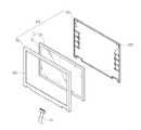
도 1은 본 발명의 제1실시예에 따른 표시장치의 분해 사시도이고, 도 2는 본 발명의 제1실시예에 따른 표시장치의 배면도이다.1 is an exploded perspective view of a display device according to a first embodiment of the present invention, and FIG. 2 is a rear view of the display device according to the first embodiment of the present invention.
표시장치(1)는 표시패널(20), 표시패널(20)의 배면에 위치한 복수의 광학필름(30), 표시패널(20)의 배면에 위치한 도광판(40), 도광판(40)의 마주하는 양측면을 따라 배치되어 있는 한 쌍의 광원부(50), 광원부(50)의 양단을 감싸고 있는 광원커버(60), 도광판(40)의 하부에 위치하는 반사판(45)과, 표시패널(20)과 연결된 구동부(80)를 포함한다. 본 발명의 일예로 표시패널(20)의 전방에는 샤시(10)가 마련되며, 반사판(45)의 후방에는 몰드부(70)가 마련된다. 이에, 표시패널(20), 광학필름(30), 도광판(40) 및 반사판(45) 등은 몰드부(70) 및 샤시(10)에 의해 체결되어 하나의 모듈로 마련된다.The
샤시(10)는 표시패널(20)의 전방에 마련되며, 표시패널(20), 광학필름(30), 도광판(40) 및 반사판(45) 등을 사이에 두고 몰드부(70)와 체결된다. 샤시(10)는 본 발명의 일예로 표시패널(20)의 가장자리를 따라 형성되며, 표시패널(20)을 등을 지지하도록 소정의 강도를 갖는 전도성있는 금속재질로 마련된다. 그러나, 샤시(10)는 이에 한정되지 않고, 구동부(80)의 회로기판(90)과 연결되어 접지역할을 할 수 있도록 적어도 일부영역에 전도성있는 다양한 재질로 마련될 수도 있다.The
표시패널(20)은 박막트랜지스터가 형성되어 있는 박막트랜지스터 기판(21)과 박막트랜지스터 기판(21)과 대면하고 있는 컬러필터 기판(22)을 포함한다. 양 기판(21, 22) 사이에는 액정층(도시하지 않음)이 위치하고 있다. 표시패널(20)은 액정층의 배열을 조정하여 화면을 형성하지만 비발광소자이기 때문에 배면에 위치한 광원부(50)로부터 빛을 공급 받아야 한다.The
구동부(80)는 박막트랜지스터 기판(21)과 연결되어 박막트랜지스터 기판(21)으로 구동신호 인가하도록 마련된다. 구동부(80)는 연성인쇄회로기판(FPC. flexible printed circuit)(81), 연성인쇄회로기판(81)에 장착되어 있는 구동칩(85), 연성인쇄회로기판(81)의 타측에 연결되어 있는 회로기판(PCB, 90)을 포함한다. 회로기판(90)은 표시패널(20)에 구동신호를 인가하며, 연성인쇄회로기판(81)의 절곡에 의해 몰드부(70)의 배면에 위치하고 있다.The
본 발명 일예로 구동부(80)는 COF(chip on film) 방식을 나타낸 것이며, TCP(tape carrier package), COG(chip on glass) 등 공지의 다른 방식도 가능하다. 또한 구동부(80)가 박막트랜지스터 기판(21)에 실장되는 것도 가능하다.In one embodiment of the present invention, the
표시패널(20)의 배면에 위치하는 광학필름(30)은 확산필름(31), 프리즘 필름(32) 및 보호필름(33)을 포함한다. 광학필름(30)의 구성은 이에 한정되지 않고 반사편광필름 등을 더 포함할 수 있다.The optical film 30 disposed on the rear surface of the
도광판(40)은 통상 폴리메틸메타아크릴레이트와 같은 아크릴 계통의 수지로 제조되며 광원부(50)로부터의 빛을 확산필름(31)에 균일하게 공급하는 역할을 한다.The
광원부(50)는 한 쌍으로 마련되며 마주하는 도광판(40)의 양 측에 각각 위치 한다. 광원부(50)는 냉음극선형광램프(CCFL) 또는 외부전극형광램프(EEFL)를 포함할 수 있다.The
광원커버(60)는 광원부(50)를 감싸면서 광원부(50)로부터의 빛을 도광판(40)으로 반사시킨다. 광원커버(60)는 알루미늄 등으로 제조될 수 있다.The
이상 설명한 도광판(40), 광원부(50) 및 광원커버(60)는 에지형 백라이트를 예시한 것으로, 본 발명은 직하형 백라이트에도 적용가능하다. 한편 광원부(50)는 발광 다이오드(LED)를 포함할 수도 있다.The
반사판(45)은 폴리에틸렌테레프탈레이트(PET)나 폴리카보네이트(PC)로 만들어질 수 있으며 은이나 알루미늄이 코팅되어 있을 수도 있다.The
도 2에 도시된 바와 같이, 몰드부(70)의 배면에 위치하는 회로기판(90)에는 후술할 전도성부재(110)가 마련되어 있다. 전도성부재(110)는 본 발명의 제1실시예로 회로기판(90)에 장착되는 커넥터(100), 회로기판(90) 상에 형성된 노출접지부(93) 및 샤시(10)를 연결한다. 커넥터(100)는 외부의 신호를 인가하는 신호케이블(130)에 연결되어 회로기판(90)에 그래픽 데이터를 공급한다(도 3참조).As shown in FIG. 2, the
이하 도 3 및 도 4를 참조하여 회로기판(90) 및 회로기판(90)에 부착된 구성에 대하여 상세히 설명한다.Hereinafter, a configuration attached to the
도 3은 본 발명의 제1실시예에 따른 표시장치의 부분 분해 사시도이고, 도 4는 도 3의 Ⅳ-Ⅳ을 따른 회로기판의 단면도이다.3 is a partially exploded perspective view of a display device according to a first exemplary embodiment of the present invention, and FIG. 4 is a cross-sectional view of a circuit board taken along line IV-IV of FIG. 3.
회로기판(90)는 표시패널(20)에 연결되어 표시패널(20)에 구동신호를 인가하는 신호배선(98)과, 접지를 위한 접지배선(99)을 포함한다. 회로기판(90)은 복수의 금속층으로 구성된다. 회로기판(90)은 본 발명의 일예로 2개의 금속층(97a,97b)으로 구성된다. 즉, 회로기판(90)은 몰드부(70)로부터 최외각에 형성된 제1절연층(95a)과, 제1절연층(95a)의 하측에 마련된 제1금속층(97a)과, 제1금속층(97a)의 하측에 마련된 중간절연층(95c)과, 중간절연층(95c)의 하측에 마련된 제2금속층(97b)과, 제2금속층(97b)의 하측에 마련된 제2절연층(95b)을 형성된다. 그러나, 회로기판(90)은 이에 한정되지 않고, 하나의 금속층 혹은 3개 이상의 금속층으로 마련될 수도 있다. 회로기판(90) 상에는 신호케이블(130)로부터 인가된 영상신호 등을 제어하도록 직접회로(IC)칩 등의 형상으로 마련된 복수의 전자부품(미도시)이 실장된다. 전자부품(미도시)은 제1절연층(95a) 혹은 제2절연층(95b) 상에 위치하며, 제1금속층(97a) 및 제2금속층(97b) 중 적어도 하나와 연결된다. 회로기판(90)에는 커넥터(100)를 지지하기 위한 커넥터 연결부(91)가 형성된다.The
제1금속층(97a) 및 제2금속층(97b)에는 전자부품(미도시)과 연결되는 신호배선(98) 및 접지배선(99)이 모두 형성될 수 있다. 그러나, 도 4에 도시된 바와 같이, 커넥터 연결부(91)에 근접한 회로기판(90)의 경우, 접지배선(99)은 제1금속층(97a)에 형성되며, 신호배선(98)은 제2금속층(97b)에 형성된다.Both the
커넥터 연결부(91)는 본 발명이 일예로 회로기판(90)의 연성인쇄회로기판(81)이 연결된 반대측에 형성된다. 그러나, 커넥터 연결부(91)는 이에 한정되지 않고, 회로기판(90)의 다른 영역에 마련될 수도 있다. 커넥터 연결부(91)는 본 발명의 일예로 커넥터(100)를 수용하도록 회로기판(90)의 일측이 함몰되도록 형성된다. 이에, 커넥터(100)가 회로기판(90) 상에 적층되도록 형성되는 경우에 비해 커 넥터(100)를 수용하도록 커넥터 연결부(91)를 형성함으로써 표시장치(1)의 두께를 더 얇게 할 수 있다. 그러나, 커넥터 연결부(91)는 회로기판(90) 상에 커넥터(100)를 지지하도록 형성될 수도 있다.The
커넥터(100)는 일측이 신호케이블(130)에 연결가능하게 마련되며, 타측이 회로기판(90)의 신호배선(98) 및 접지배선(99)에 연결된다. 커넥터(100)는 적어도 일부가 전도성재질로 형성된 하우징(101)과, 신호케이블(130)과 연결가능하게 마련되어 있는 연결단(103)과, 회로기판(90)의 신호배선(98)에 연결되어 있는 신호핀(105)과, 회로기판(90)의 접지배선(99) 및 하우징(101)의 전도성재질과 연결되어 있는 접지핀(107)을 포함한다. 커넥터(100)의 양측에는 커넥터 연결부(91)에 지지되어 솔더링 등의 방법으로 결합되는 지지부(109)가 마련된다.One end of the
하우징(101)은 연결단(103), 신호핀(105) 및 접지핀(107)을 지지하도록 커넥터(100)의 외각에 형성된다. 본 발명의 일예로 하우징(101)은 연결단(103), 신호핀(105) 및 접지핀(107)을 지지하는 절연재질로 형성된 절연체(101a)와, 접지핀(107)과 연결되는 전도성 재질로 형성된 전도체(101b)를 포함한다. 그리고, 신호핀(105) 및 접지핀(107)의 일측은 각각 연결단(103)과 연결되며, 타측은 각각 회로기판(90)의 신호배선(98) 및 접지배선(99)에 연결된다.The
절연체(101a)는 신호핀(105)과 접지핀(107)이 서로 전기가 통하지 않도록 절연시킨다. 전도체(101b)는 접지핀(107)과 연결되며, 후술할 전도성부재(110)에 의해 샤시(10)와 연결된다.The
본 발명에 따른 표시장치(1)는 커넥터(100)와 인접한 회로기판(90) 상에 접 지배선(99)의 일부가 노출되어 있는 노출접지부(93)와, 노출접지부(93)를 샤시(10)와 연결하는 전도성부재(110)를 더 포함한다. 그리고, 본 발명에 따른 표시장치(1)는 회로기판(90)과 전도성부재(110) 사이에 마련된 절연부재(120)를 더 포함할 수 있다.In the
노출접지부(93)는 커넥터(100)에 근접한 회로기판(90)의 접지배선(99) 상에 형성된 절연층의 일부를 형성하지 않거나 제거하여 접지배선(99)의 일부를 노출시켜 형성한다. 본 발명의 일예로 노출접지부(93)가 형성되는 접지배선(99)은 전도성부재(110)와 가장 근접한 제1금속층(97a)에 형성된다. 이에, 커넥터(100)에 근접한 접지배선(99)이 최외각 금속층인 제1금속층(97a)에 형성되어 노출접지부(93)를 형성하기 위해서는 제1절연층(95a)만 형성하지 않거나 제거하면 되므로, 노출접지부(93)를 용이하게 형성할 수 있다. 그러나, 커넥터(100)에 근접한 접지배선(99)은 제2금속층(97b)에 형성될 수도 있다.The exposed
노출접지부(93)는 본 발명의 일예로 사각형상으로 마련된다. 즉, 본 발명의 일예로 노출접지부(93)의 폭은 4mm정도이고, 길이는 36mm정도이다. 그러나, 노출접지부(93)의 형상은 전도성부재(110)가 용이하게 접촉할 수 있도록 원형, 타원형 혹은 다른 다각형 형상 등 다양하게 마련될 수 있다. 노출접지부(93)는 전도성부재(110)가 용이하게 접촉할 수 있도록 충분한 넓이로 형성되는 것이 바람직하다. 본 발명의 일예로 노출접지부(93)는 커넥터(100)의 평면 넓이와 비슷하게 마련되나, 전도성부재(110)와 용이하게 접촉하도록 충분한 넓이를 확보하기 위해 커넥터(100)의 평면의 넓이보다 크게 마련될 수도 있다. 그러나, 전도성부재(110)가 용 이하게 접촉할 수 있다면, 커넥터(100)의 평면의 넓이보다 작게 마련될 수도 있다.The exposed
전도성부재(110)는 본 발명의 일예로 알루미늄 테이프를 포함한다. 전도성부재(110)은 노출접지부(93), 하우징(101)의 전도체(101b) 및 샤시(10)를 전기적으로 연결하도록 알루미늄 테이프로 마련된다. 이에, 작업자가 노출접지부(93), 하우징(101)의 전도체(101b) 및 샤시(10)에 전도성부재(110)인 알루미늄 테이프를 부착하면 되므로 작업이 용이하다. 그러나, 전도성부재(110)를 이에 한정되지 않고, 노출접지부(93), 하우징(101)의 전도체(101b) 및 샤시(10)를 전기적으로 연결할 수 있는 구리테이프와 같은 다양한 재질의 테이프나 전도성부재로 마련될 수도 있다. 이러한 구성에 의해, 커넥터(100) 및 커넥터(100)와 인접한 접지배선(99)을 직접적으로 샤시(10)에 접지시킬 수 있다.The
절연부재(120)는 노출접지부(93)와 샤시(10) 사이에 위치하는 회로기판(90)의 판면에 부착된다. 본 발명의 일예로 절연부재(120)는 전도성부재(110)와 접촉하는 노출접지부(93) 및 커넥터(100)을 제외한 회로기판(90)의 판면 및 몰드부(70)의 일영역에 부착되어 회로기판(90)을 몰드부(70)에 부착시킨다. 이에, 절연부재(120)에 의해 전도성부재(110)가 회로기판(90)에 실장된 전자부품(미도시) 등과 전기적으로 연결되는 것을 방지할 수 있으며, 회로기판(90)을 몰드부(70)에 부착시킬 수 있다. 절연부재(120)는 본 발명의 일예로 회로기판(90)을 몰드부(70)의 배면에 부착하는 투명한 절연테이프를 포함한다. 즉, 절연부재(120)는 본 발명의 일예로 투명한 접착테이프라 같은 절연테이프로 마련된다. 그러나, 절연부재(120)는 이에 한정하고 않고, 전도성부재(110)와 회로기판(90) 사이를 절연하며, 회로기판(90)을 몰드부(70)에 부착시킬 수 있는 다양한 형태의 재질로 마련될 수 있다.The insulating
도 5은 본 발명의 제1실시예에 따른 표시장치의 제조과정을 나타낸 순서도이다. 이 도면을 기초로 표시장치의 제조방법을 설명한다.5 is a flowchart illustrating a manufacturing process of a display device according to a first embodiment of the present invention. The manufacturing method of the display apparatus is demonstrated based on this drawing.
우선, 표시패널(20)과, 표시패널(20)과 연결되는 회로기판(90)과, 회로기판(90)에 장착되는 커넥터(100)를 각각 마련한 상태에서, 회로기판(90) 상에 커넥터(100)와 인접하게 회로기판(90)의 접지배선(99)의 일부가 노출되도록 노출접지부(93)를 형성한다(S1). 그리고, 회로기판(90)에 커넥터(100)를 장착하며, 커넥터(100)가 장착된 회로기판(90)을 표시패널(20)에 연결한 후, 표시패널(20)의 전방에는 샤시(10)를 마련하며, 표시패널(20)의 후방에 몰드부(70)를 마련하고, 회로기판(90)을 몰드부(70)의 배면에 배치한다(S3). 그리고, 노출접지부(93)와 샤시(10) 사이에 위치하는 회로기판(90) 상에 절연부재(120)를 배치한다(S5). 이때, 절연부재(120)는 절연테이프로 마련되어 전도성부재(110)와 접촉하는 노출접지부(93) 및 커넥터(100)을 제외한 회로기판(90)의 판면 및 몰드부(70)의 일영역에 부착되어 회로기판(90)을 몰드부(70)에 부착시킨다. 그런 후, 노출접지부(93) 및 커넥터(100)를 샤시(10)와 연결하는 전도성부재(110)를 마련한다(S9). 이때, 본 발명이 일예로 전도성부재(110)를 알루미늄 테이프로 마련하여, 노출접지부(93), 하우징(101)의 전도체(101b) 및 샤시(10)에 부착함으로써 노출접지부(93), 하우징(101)의 전도체(101b) 및 샤시(10)를 용이하게 전기적으로 연결할 수 있다.First, the
전술한 제조과정의 순서는 본 발명의 일예를 나타낸 것으로 제조환경이나 제조기술에 따라서 제조과정의 순서가 변경될 수도 있다.The order of the manufacturing process described above shows an example of the present invention, and the order of the manufacturing process may be changed according to a manufacturing environment or a manufacturing technique.
이러한 구성에 의해, 본 발명의 제1실시예에 따른 표시장치는 전도성부재를 사용하여 커넥터 및 노출접지부을 직접적으로 샤시에 접지시킴으로서, 외부 신호를 인가하는 신호케이블이 회로기판의 커넥터에 연결되어 발생되는 EMI(electromagnetic interference) 등을 용이하게 차단하여 노이즈를 최소화 할 수 있다.With this configuration, the display device according to the first embodiment of the present invention directly connects the connector and the exposed ground portion to the chassis by using a conductive member, so that a signal cable for applying an external signal is connected to the connector of the circuit board. EMI can be minimized by easily blocking electromagnetic interference (EMI).
그리고, 본 발명의 제1실시예에 따른 표시장치는 절연부재를 사용하여 전도성부재가 회로기판에 실장된 전자부품 등과 전기적으로 연결되는 것을 방지할 수 있으며, 회로기판을 몰드부에 부착시킬 수 있다.In addition, the display device according to the first embodiment of the present invention can prevent the conductive member from being electrically connected to the electronic component mounted on the circuit board by using an insulating member, and can attach the circuit board to the mold part. .
제2실시예,Second embodiment,
도 6은 본 발명의 제2실시예에 따른 표시장치의 배면도이다. 이 도면을 기초로 제2실시예에 따른 표시장치(200)가 제1실시예와 상이한 점에 대해 설명한다.6 is a rear view of the display device according to the second embodiment of the present invention. Based on this drawing, the difference between the display device 200 according to the second embodiment and the first embodiment will be described.
제2실시예에 따른 표시장치(200)는 역시 몰드부(70)의 배면에 회로기판(90)이 배치되어, 절연부재(120)에 의해 부착된다. 그러나, 제2실시예에 따른 표시장치(200)에 마련된 전도성부재(210)는 제1실시예와 달리, 노출접지부(93) 및 샤시(10)를 전기적으로 연결할 뿐, 커넥터(220)는 연결하지 않는다.In the display device 200 according to the second exemplary embodiment, the
이와 같이, 전도성부재(210)가 커넥터(220)와 연결되지 않는 경우는, 커넥터(220)가 전도성재질로 마련되어 있지 않은 경우이거나 전도성부재(210)가 부착되는 커넥터(220)의 평면이 너무 좁아 전도성부재를 용이하게 부착할 없는 경우 등이다.As such, when the conductive member 210 is not connected to the connector 220, the connector 220 is not made of a conductive material or the plane of the connector 220 to which the conductive member 210 is attached is too narrow. This is the case where the conductive member cannot be easily attached.
또한, 부착되는 커넥터(220)의 평면이 좁은데 무리하게 전도성부재(210)를 부착할 경우, 신호케이블(130)이 커넥터(220)와 연결된 상태에서 전도성부재(210)와 접촉되는 것을 방지하기 위한 것이다.In addition, when the plane of the connector 220 to be attached is too narrow, when the conductive member 210 is forcibly attached, the
이러한 구성에 의해, 본 발명의 제2실시예에 따른 표시장치는 전도성부재를 사용하여 노출접지부을 직접적으로 샤시에 접지시킴으로서, 외부 신호를 인가하는 신호케이블이 회로기판의 커넥터에 연결되어 발생되는 EMI(electromagnetic interference) 등을 용이하게 차단하여 노이즈를 최소화 할 수 있다.With this configuration, the display device according to the second embodiment of the present invention directly grounds the exposed ground portion to the chassis by using a conductive member, whereby a signal cable for applying an external signal is connected to a connector of a circuit board. (Electromagnetic interference) can be easily blocked to minimize noise.
도 7 및 도 8은 본 발명에 따른 표시장치가 장착된 휴대용 컴퓨터의 사시도 및 부분 분해 사시도이다. 이 도면들을 기초로 하여, 본 발명에 따른 표시장치가 장착된 휴대용 컴퓨터에 대해 설명한다. 본 발명에 따른 휴대용 컴퓨터에 장착된 표시장치는 전술한 실시예와 유사하므로 표시장치에 대한 도면 및 상세한 설명은 전술한 실시예를 따른다.7 and 8 are a perspective view and a partially exploded perspective view of a portable computer equipped with a display device according to the present invention. Based on these drawings, a portable computer equipped with a display device according to the present invention will be described. Since the display device mounted on the portable computer according to the present invention is similar to the above-described embodiment, the drawings and detailed description of the display device follow the above-described embodiment.
본 발명에 따른 휴대용 컴퓨터(300)는 컴퓨터본체(310)와, 컴퓨터본체(310)에 회동가능하게 결합된 디스플레이(320)를 포함한다.The
컴퓨터본체(310)는 내부에 장착된 중앙처리장치(CPU) 및 메모리장치와 같은 전자부품(미도시)과, 키보드(311)와 같은 입력장치를 포함한다. 컴퓨터본체(310)는 디스플레이(320)와 회동가능하게 결합되도록 디스플레이(320)와 힌지부(301)에 의해 결합된다. 컴퓨터본체(310)에는 컴퓨터본체(310)로부터 연장된 신호케이블(130)이 마련된다.The
신호케이블(130)은 표시장치(1)의 배면에 마련된 커넥터(100)에 연결되어 컴퓨터본체(310)로부터 그래픽 데이터를 회로기판(90)에 공급하게 된다. 신호케이 블(130)은 본 발명의 일예로 힌지부(301)를 통해 컴퓨터본체(310)로 연결되며, 이러한 연결구조는 공지 기술에 해당하므로 자세한 설명은 생략한다.The
디스플레이(320)는 화상을 형성하는 표시장치(1)과, 표시장치(1)의 전방에 마련된 전방커버(321)와, 표시장치(1)의 후방에 마련된 후방커버(325)를 포함한다.The
전방커버(321)에는 표시패널(20)의 표시영역이 노출되도록 개구부(322)가 마련된다. 전방커버(321)는 표시패널(20)의 가장자리를 차단하며 스크루나 후크결합 등에 의해 후방커버(325)와 결합된다.The
디스플레이(320)에는 전방커버(321) 및 후방커버(325)사이에 안테나(305)가 마련된다. 휴대용 컴퓨터(300)는 안테나(305)를 사용하여 무선광역통신망(WWAN, wireless wide area network)을 통해 인터넷 등에 접속할 수 있다. 안테나(305)는 본 발명의 일예로 디스플레이(320)의 표시장치(1) 상측에 배치된다. 그러나, 안테나(305)는 표시장치(1)의 측면이나 하측에 배치될 수도 있으며, 컴퓨터본체(310)에 배치될 수도 있다. 이러한 안테나(305)에 대한 구조나 기능은 공지의 기술에 해당하여 상세한 설명을 생략한다.The
이러한 구성에 의해, 본 발명에 따른 휴대용 컴퓨터는 전술한 표시장치에서와 같이 전도성부재를 사용하여 커넥터 및 노출접지부을 직접적으로 샤시에 접지시켜, 외부 신호를 인가하는 신호케이블이 회로기판의 커넥터에 연결되어 발생되는 EMI(electromagnetic interference) 등을 용이하게 차단하여 안테나에서 검출되는 노이즈를 최소화 할 수 있다.With this configuration, the portable computer according to the present invention uses the conductive member to ground the connector and the exposed ground portion directly to the chassis, as in the display device described above, so that a signal cable for applying an external signal is connected to the connector of the circuit board. It is possible to minimize the noise detected by the antenna by easily blocking the generated electromagnetic interference (EMI).
특히, 본 발명에 따른 휴대용 컴퓨터는 신호케이블이 휴대용 컴퓨터에서 주 로 사용되는 그래픽 데이터 전송방식인 LVDS(low voltage differential signaling)방식을 통해 그래픽 데이터를 회로기판으로 전송할 경우, 휴대전화에 사용되는 무선대역인 850Mhz, 900Mhz, 1.8Ghz, 1.9Ghz, 2.1Ghz 등 다양한 주파수 대역에서 EMI(electromagnetic interference) 등을 용이하게 차단하여 노이즈를 최소화 할 수 있다.In particular, the portable computer according to the present invention is a radio band used for a mobile phone when the signal cable transmits the graphic data to the circuit board through the low voltage differential signaling (LVDS) method, which is a graphic data transmission method mainly used in the portable computer Noise can be minimized by easily blocking electromagnetic interference (EMI) in various frequency bands such as 850Mhz, 900Mhz, 1.8Ghz, 1.9Ghz, 2.1Ghz.
비록 본발명의 몇몇 실시예들이 도시되고 설명되었지만, 본발명이 속하는 기술분야의 통상의 지식을 가진 당업자라면 본발명의 원칙이나 정신에서 벗어나지 않으면서 본 실시예를 변형할 수 있음을 알 수 있을 것이다. 본발명의 범위는 첨부된 청구항과 그 균등물에 의해 정해질 것이다.Although some embodiments of the invention have been shown and described, those skilled in the art will recognize that modifications can be made to the embodiments without departing from the spirit or principles of the invention. . It is intended that the scope of the invention be defined by the claims appended hereto and their equivalents.
도 1은 본 발명의 제1실시예에 따른 표시장치의 분해 사시도,1 is an exploded perspective view of a display device according to a first embodiment of the present invention;
도 2는 본 발명의 제1실시예에 따른 표시장치의 배면도,2 is a rear view of the display device according to the first embodiment of the present invention;
도 3은 도 2의 표시장치의 부분 분해 사시도,3 is a partially exploded perspective view of the display device of FIG. 2;
도 4는 도 3의 Ⅳ-Ⅳ을 따른 회로기판의 단면도,4 is a cross-sectional view of the circuit board taken along line IV-IV of FIG. 3;
도 5는 본 발명의 제1실시예에 따른 표시장치의 제조과정을 나타낸 순서도,5 is a flowchart illustrating a manufacturing process of a display device according to a first embodiment of the present invention;
도 6은 본 발명의 제2실시예에 따른 표시장치의 배면도,6 is a rear view of the display device according to the second embodiment of the present invention;
도 7은 본 발명에 따른 표시장치가 장착된 휴대용 컴퓨터의 사시도,7 is a perspective view of a portable computer equipped with a display device according to the present invention;
도 8은 도 7의 휴대용 컴퓨터의 부분 분해 사시도이다.8 is a partially exploded perspective view of the portable computer of FIG. 7.
* 도면의 주요부분의 부호에 대한 설명 *Explanation of Signs of Major Parts of Drawings
1 : 표시장치 10 : 샤시1: display device 10: chassis
20 : 표시패널 70 : 몰드부20: display panel 70: mold part
80 : 구동부 90 : 회로기판80: drive unit 90: circuit board
93 : 노출접지부 98 : 신호배선93: exposed ground portion 98: signal wiring
99 : 접지배선 100 : 커넥터99: grounding wiring 100: connector
101 : 하우징 110 : 전도성부재101
120 : 절연부재 130 : 신호케이블120: insulation member 130: signal cable
Claims (19)
Translated fromKoreanPriority Applications (2)
| Application Number | Priority Date | Filing Date | Title |
|---|---|---|---|
| KR1020070118070AKR101427589B1 (en) | 2007-11-19 | 2007-11-19 | A portable computer having a display device, a method of manufacturing the display device, and a display device |
| US12/168,643US8000093B2 (en) | 2007-11-19 | 2008-07-07 | Display device, manufacturing method of the display device, and portable computer having the display device |
Applications Claiming Priority (1)
| Application Number | Priority Date | Filing Date | Title |
|---|---|---|---|
| KR1020070118070AKR101427589B1 (en) | 2007-11-19 | 2007-11-19 | A portable computer having a display device, a method of manufacturing the display device, and a display device |
Publications (2)
| Publication Number | Publication Date |
|---|---|
| KR20090051601Atrue KR20090051601A (en) | 2009-05-22 |
| KR101427589B1 KR101427589B1 (en) | 2014-08-07 |
Family
ID=40641706
Family Applications (1)
| Application Number | Title | Priority Date | Filing Date |
|---|---|---|---|
| KR1020070118070AExpired - Fee RelatedKR101427589B1 (en) | 2007-11-19 | 2007-11-19 | A portable computer having a display device, a method of manufacturing the display device, and a display device |
Country Status (2)
| Country | Link |
|---|---|
| US (1) | US8000093B2 (en) |
| KR (1) | KR101427589B1 (en) |
Cited By (1)
| Publication number | Priority date | Publication date | Assignee | Title |
|---|---|---|---|---|
| US8593610B2 (en) | 2010-05-13 | 2013-11-26 | Samsung Display Co., Ltd. | Liquid crystal display device |
Families Citing this family (7)
| Publication number | Priority date | Publication date | Assignee | Title |
|---|---|---|---|---|
| TWI396152B (en)* | 2009-06-26 | 2013-05-11 | Au Optronics Corp | Display device |
| KR20110003654A (en)* | 2009-07-06 | 2011-01-13 | 삼성전자주식회사 | Plasma display device |
| US8761683B2 (en)* | 2009-08-28 | 2014-06-24 | Apple Inc. | Electronic device instructions provided using radio signals |
| US8988628B2 (en)* | 2011-06-23 | 2015-03-24 | Apple Inc. | Coated chassis for liquid crystal display |
| CN102855850A (en)* | 2011-06-28 | 2013-01-02 | 鸿富锦精密工业(深圳)有限公司 | Electronic device and liquid crystal display module |
| KR102078299B1 (en) | 2013-04-02 | 2020-02-18 | 삼성디스플레이 주식회사 | Display appatus having anttena |
| IT201700004156A1 (en)* | 2017-01-17 | 2018-07-17 | Carel Ind Spa | DISPLAY STRUCTURE FOR CONTROL SYSTEMS |
Family Cites Families (21)
| Publication number | Priority date | Publication date | Assignee | Title |
|---|---|---|---|---|
| US5587887A (en)* | 1995-05-01 | 1996-12-24 | Apple Computer, Inc. | Printed circuit board having a configurable voltage supply |
| KR19980067764A (en) | 1997-02-12 | 1998-10-15 | 김광호 | Grounding Structure of Printed Circuit Board for LCD |
| US6211457B1 (en)* | 1997-12-18 | 2001-04-03 | Eastman Kodak Company | EMI-shielded connector in an electronic device |
| KR100407993B1 (en)* | 2001-06-01 | 2003-12-03 | 엘지.필립스 엘시디 주식회사 | Shield cover of Liquid Crystal Display |
| JP2003044166A (en)* | 2001-07-27 | 2003-02-14 | Nec Miyagi Ltd | Liquid crystal screen part attachable and detachable notebook type personal computer |
| JP3814503B2 (en) | 2001-08-30 | 2006-08-30 | 株式会社日立製作所 | Image display device |
| KR100906961B1 (en) | 2002-12-30 | 2009-07-08 | 삼성전자주식회사 | Flat Panel Display |
| KR100568177B1 (en)* | 2003-06-23 | 2006-04-05 | 삼성전자주식회사 | Connector and Notebook Computer Using the Same |
| JP2005215555A (en) | 2004-01-30 | 2005-08-11 | Fujitsu Hitachi Plasma Display Ltd | Display device and display panel device |
| KR100637149B1 (en) | 2004-02-20 | 2006-10-20 | 삼성에스디아이 주식회사 | Plasma display device |
| US7508673B2 (en) | 2004-03-04 | 2009-03-24 | Samsung Sdi Co., Ltd. | Heat dissipating apparatus for plasma display device |
| KR20060070871A (en) | 2004-12-21 | 2006-06-26 | 삼성전자주식회사 | LCD Display |
| KR101107695B1 (en)* | 2004-12-29 | 2012-01-25 | 엘지디스플레이 주식회사 | Printed Circuit Board for Liquid Crystal Display |
| KR20060090392A (en) | 2005-02-07 | 2006-08-10 | 삼성전자주식회사 | Flat panel display for EMI shielding |
| KR20060112142A (en) | 2005-04-26 | 2006-10-31 | 삼성전자주식회사 | Flat Panel Display |
| KR101129432B1 (en) | 2005-05-26 | 2012-03-26 | 삼성전자주식회사 | Liquid crystal display |
| KR101152125B1 (en) | 2005-05-26 | 2012-06-15 | 삼성전자주식회사 | Display device |
| KR20070023271A (en) | 2005-08-24 | 2007-02-28 | 삼성전자주식회사 | Display device and manufacturing method thereof |
| KR20070066116A (en) | 2005-12-21 | 2007-06-27 | 삼성전자주식회사 | LCD Display |
| KR20070077682A (en)* | 2006-01-24 | 2007-07-27 | 삼성전자주식회사 | Display |
| JP2007199501A (en) | 2006-01-27 | 2007-08-09 | Optrex Corp | Image display device |
- 2007
- 2007-11-19KRKR1020070118070Apatent/KR101427589B1/ennot_activeExpired - Fee Related
- 2008
- 2008-07-07USUS12/168,643patent/US8000093B2/ennot_activeExpired - Fee Related
Cited By (1)
| Publication number | Priority date | Publication date | Assignee | Title |
|---|---|---|---|---|
| US8593610B2 (en) | 2010-05-13 | 2013-11-26 | Samsung Display Co., Ltd. | Liquid crystal display device |
Also Published As
| Publication number | Publication date |
|---|---|
| US8000093B2 (en) | 2011-08-16 |
| KR101427589B1 (en) | 2014-08-07 |
| US20090129005A1 (en) | 2009-05-21 |
Similar Documents
| Publication | Publication Date | Title |
|---|---|---|
| US6667780B2 (en) | Liquid crystal display module and liquid crystal display apparatus having the same | |
| US7365812B2 (en) | Flat panel display apparatus with grounded PCB | |
| US7206037B2 (en) | Display module and display unit | |
| US8212961B2 (en) | Backlight for liquid crystal display device having a first FPCB mounting a plurality of light emitting diodes connecting a second FPCB via a through hole formed on a lower cover | |
| US7567314B2 (en) | Flat panel display apparatus having fixing member to secure display module | |
| KR101427589B1 (en) | A portable computer having a display device, a method of manufacturing the display device, and a display device | |
| EP1903376B1 (en) | Liquid crystal display device and portable display apparatus using the same | |
| US7894035B2 (en) | Driving device and a liquid crystal display including the same | |
| US7670019B2 (en) | Backlight assembly, liquid crystal display having the same and method thereof | |
| US20040041960A1 (en) | Mold frame structure of liquid crystal display | |
| US20080096402A1 (en) | Connector for a display apparatus | |
| KR20080038592A (en) | Flexible printed circuit board and liquid crystal display device having same | |
| US7524210B2 (en) | Backlight unit and liquid crystal display device having the same | |
| KR20080018718A (en) | Liquid crystal display | |
| EP3683620B1 (en) | Display apparatus | |
| KR101123529B1 (en) | Liquid Crystal Display device and the fabrication method | |
| US8471978B2 (en) | Driving device and a liquid crystal display including the same | |
| CN216979519U (en) | ESD (electro-static discharge) prevention display module and display equipment | |
| KR101002931B1 (en) | LCD Display | |
| KR20130029309A (en) | Liquid crystal display apparatus | |
| KR20080028580A (en) | Liquid crystal display | |
| KR20060060841A (en) | Flat panel display device with enhanced tightening force between parts | |
| KR20040004917A (en) | Liquid crystal display | |
| KR20070067896A (en) | LCD Display | |
| KR20080041892A (en) | Liquid crystal display |
Legal Events
| Date | Code | Title | Description |
|---|---|---|---|
| PA0109 | Patent application | St.27 status event code:A-0-1-A10-A12-nap-PA0109 | |
| R17-X000 | Change to representative recorded | St.27 status event code:A-3-3-R10-R17-oth-X000 | |
| PG1501 | Laying open of application | St.27 status event code:A-1-1-Q10-Q12-nap-PG1501 | |
| R18-X000 | Changes to party contact information recorded | St.27 status event code:A-3-3-R10-R18-oth-X000 | |
| N231 | Notification of change of applicant | ||
| PN2301 | Change of applicant | St.27 status event code:A-3-3-R10-R13-asn-PN2301 St.27 status event code:A-3-3-R10-R11-asn-PN2301 | |
| A201 | Request for examination | ||
| PA0201 | Request for examination | St.27 status event code:A-1-2-D10-D11-exm-PA0201 | |
| D13-X000 | Search requested | St.27 status event code:A-1-2-D10-D13-srh-X000 | |
| D14-X000 | Search report completed | St.27 status event code:A-1-2-D10-D14-srh-X000 | |
| E902 | Notification of reason for refusal | ||
| PE0902 | Notice of grounds for rejection | St.27 status event code:A-1-2-D10-D21-exm-PE0902 | |
| E13-X000 | Pre-grant limitation requested | St.27 status event code:A-2-3-E10-E13-lim-X000 | |
| P11-X000 | Amendment of application requested | St.27 status event code:A-2-2-P10-P11-nap-X000 | |
| P13-X000 | Application amended | St.27 status event code:A-2-2-P10-P13-nap-X000 | |
| E701 | Decision to grant or registration of patent right | ||
| PE0701 | Decision of registration | St.27 status event code:A-1-2-D10-D22-exm-PE0701 | |
| GRNT | Written decision to grant | ||
| PR0701 | Registration of establishment | St.27 status event code:A-2-4-F10-F11-exm-PR0701 | |
| PR1002 | Payment of registration fee | St.27 status event code:A-2-2-U10-U11-oth-PR1002 Fee payment year number:1 | |
| PG1601 | Publication of registration | St.27 status event code:A-4-4-Q10-Q13-nap-PG1601 | |
| R18-X000 | Changes to party contact information recorded | St.27 status event code:A-5-5-R10-R18-oth-X000 | |
| LAPS | Lapse due to unpaid annual fee | ||
| PC1903 | Unpaid annual fee | St.27 status event code:A-4-4-U10-U13-oth-PC1903 Not in force date:20170802 Payment event data comment text:Termination Category : DEFAULT_OF_REGISTRATION_FEE | |
| PC1903 | Unpaid annual fee | St.27 status event code:N-4-6-H10-H13-oth-PC1903 Ip right cessation event data comment text:Termination Category : DEFAULT_OF_REGISTRATION_FEE Not in force date:20170802 | |
| R18-X000 | Changes to party contact information recorded | St.27 status event code:A-5-5-R10-R18-oth-X000 |