KR20090042984A - Nearly flat visible light emission and / or light emitting structures - Google Patents
Nearly flat visible light emission and / or light emitting structuresDownload PDFInfo
- Publication number
- KR20090042984A KR20090042984AKR1020097005784AKR20097005784AKR20090042984AKR 20090042984 AKR20090042984 AKR 20090042984AKR 1020097005784 AKR1020097005784 AKR 1020097005784AKR 20097005784 AKR20097005784 AKR 20097005784AKR 20090042984 AKR20090042984 AKR 20090042984A
- Authority
- KR
- South Korea
- Prior art keywords
- light emitting
- electrode
- dielectric
- visible light
- less
- Prior art date
- Legal status (The legal status is an assumption and is not a legal conclusion. Google has not performed a legal analysis and makes no representation as to the accuracy of the status listed.)
- Ceased
Links
- 239000004020conductorSubstances0.000claimsabstractdescription60
- 239000011229interlayerSubstances0.000claimsabstractdescription57
- 230000001681protective effectEffects0.000claimsabstractdescription40
- 229920006254polymer filmPolymers0.000claimsabstractdescription11
- 230000005684electric fieldEffects0.000claimsabstractdescription8
- 239000011521glassSubstances0.000claimsdescription55
- 239000010410layerSubstances0.000claimsdescription43
- 239000007789gasSubstances0.000claimsdescription30
- 239000000463materialSubstances0.000claimsdescription18
- 229920002037poly(vinyl butyral) polymerPolymers0.000claimsdescription18
- 238000000034methodMethods0.000claimsdescription16
- 239000004417polycarbonateSubstances0.000claimsdescription14
- 229920000515polycarbonatePolymers0.000claimsdescription14
- IJGRMHOSHXDMSA-UHFFFAOYSA-NAtomic nitrogenChemical compoundN#NIJGRMHOSHXDMSA-UHFFFAOYSA-N0.000claimsdescription12
- VYPSYNLAJGMNEJ-UHFFFAOYSA-NSilicium dioxideChemical compoundO=[Si]=OVYPSYNLAJGMNEJ-UHFFFAOYSA-N0.000claimsdescription10
- -1polyethylene terephthalatePolymers0.000claimsdescription9
- 229920000139polyethylene terephthalatePolymers0.000claimsdescription8
- 239000005020polyethylene terephthalateSubstances0.000claimsdescription8
- 239000003989dielectric materialSubstances0.000claimsdescription6
- 229910052757nitrogenInorganic materials0.000claimsdescription6
- 239000004814polyurethaneSubstances0.000claimsdescription6
- 239000005361soda-lime glassSubstances0.000claimsdescription6
- 229920002635polyurethanePolymers0.000claimsdescription5
- VGGSQFUCUMXWEO-UHFFFAOYSA-NEtheneChemical compoundC=CVGGSQFUCUMXWEO-UHFFFAOYSA-N0.000claimsdescription4
- 239000005977EthyleneSubstances0.000claimsdescription4
- XTXRWKRVRITETP-UHFFFAOYSA-NVinyl acetateChemical compoundCC(=O)OC=CXTXRWKRVRITETP-UHFFFAOYSA-N0.000claimsdescription4
- 230000003287optical effectEffects0.000claimsdescription4
- 229920003229poly(methyl methacrylate)Polymers0.000claimsdescription4
- 239000004926polymethyl methacrylateSubstances0.000claimsdescription4
- 239000010453quartzSubstances0.000claimsdescription4
- 239000004698PolyethyleneSubstances0.000claimsdescription3
- PNEYBMLMFCGWSK-UHFFFAOYSA-Naluminium oxideInorganic materials[O-2].[O-2].[O-2].[Al+3].[Al+3]PNEYBMLMFCGWSK-UHFFFAOYSA-N0.000claimsdescription3
- 239000005388borosilicate glassSubstances0.000claimsdescription3
- 229920000573polyethylenePolymers0.000claimsdescription3
- 239000011112polyethylene naphthalateSubstances0.000claimsdescription3
- 239000004800polyvinyl chlorideSubstances0.000claimsdescription3
- 239000000377silicon dioxideSubstances0.000claimsdescription3
- XLYOFNOQVPJJNP-UHFFFAOYSA-NwaterSubstancesOXLYOFNOQVPJJNP-UHFFFAOYSA-N0.000claimsdescription3
- 238000003848UV Light-CuringMethods0.000claimsdescription2
- 229910052782aluminiumInorganic materials0.000claimsdescription2
- XAGFODPZIPBFFR-UHFFFAOYSA-NaluminiumChemical compound[Al]XAGFODPZIPBFFR-UHFFFAOYSA-N0.000claimsdescription2
- 235000013361beverageNutrition0.000claimsdescription2
- 239000002537cosmeticSubstances0.000claimsdescription2
- 238000001035dryingMethods0.000claimsdescription2
- 230000005611electricityEffects0.000claimsdescription2
- 235000013305foodNutrition0.000claimsdescription2
- 239000011261inert gasSubstances0.000claimsdescription2
- 238000005192partitionMethods0.000claimsdescription2
- 229920003207poly(ethylene-2,6-naphthalate)Polymers0.000claimsdescription2
- 229920000642polymerPolymers0.000claimsdescription2
- 229920000915polyvinyl chloridePolymers0.000claimsdescription2
- 239000008399tap waterSubstances0.000claimsdescription2
- 235000020679tap waterNutrition0.000claimsdescription2
- 229920006289polycarbonate filmPolymers0.000claims2
- 239000000725suspensionSubstances0.000claims1
- OAICVXFJPJFONN-UHFFFAOYSA-NPhosphorusChemical compound[P]OAICVXFJPJFONN-UHFFFAOYSA-N0.000abstractdescription3
- 239000000758substrateSubstances0.000description15
- 238000000576coating methodMethods0.000description9
- 239000011248coating agentSubstances0.000description8
- 229910052751metalInorganic materials0.000description8
- 239000002184metalSubstances0.000description8
- 239000011295pitchSubstances0.000description8
- 229920003023plasticPolymers0.000description8
- 239000002985plastic filmSubstances0.000description7
- 239000000615nonconductorSubstances0.000description6
- 230000006911nucleationEffects0.000description6
- 238000010899nucleationMethods0.000description6
- 239000004033plasticSubstances0.000description6
- 229920006255plastic filmPolymers0.000description5
- 230000002829reductive effectEffects0.000description5
- XKRFYHLGVUSROY-UHFFFAOYSA-NArgonChemical compound[Ar]XKRFYHLGVUSROY-UHFFFAOYSA-N0.000description4
- 229910052736halogenInorganic materials0.000description4
- 150000002367halogensChemical class0.000description4
- 238000005286illuminationMethods0.000description4
- 229910044991metal oxideInorganic materials0.000description4
- 150000004706metal oxidesChemical class0.000description4
- BASFCYQUMIYNBI-UHFFFAOYSA-NplatinumChemical compound[Pt]BASFCYQUMIYNBI-UHFFFAOYSA-N0.000description4
- 125000006850spacer groupChemical group0.000description4
- 229910052724xenonInorganic materials0.000description4
- FHNFHKCVQCLJFQ-UHFFFAOYSA-Nxenon atomChemical compound[Xe]FHNFHKCVQCLJFQ-UHFFFAOYSA-N0.000description4
- 229920002799BoPETPolymers0.000description3
- ZLMJMSJWJFRBEC-UHFFFAOYSA-NPotassiumChemical compound[K]ZLMJMSJWJFRBEC-UHFFFAOYSA-N0.000description3
- BQCADISMDOOEFD-UHFFFAOYSA-NSilverChemical compound[Ag]BQCADISMDOOEFD-UHFFFAOYSA-N0.000description3
- 239000000956alloySubstances0.000description3
- 229910045601alloyInorganic materials0.000description3
- 230000008859changeEffects0.000description3
- 230000002093peripheral effectEffects0.000description3
- 239000002861polymer materialSubstances0.000description3
- 229910052700potassiumInorganic materials0.000description3
- 239000011591potassiumSubstances0.000description3
- 239000000047productSubstances0.000description3
- 229910052709silverInorganic materials0.000description3
- 239000004332silverSubstances0.000description3
- XOLBLPGZBRYERU-UHFFFAOYSA-Ntin dioxideChemical compoundO=[Sn]=OXOLBLPGZBRYERU-UHFFFAOYSA-N0.000description3
- 229910001887tin oxideInorganic materials0.000description3
- 239000005341toughened glassSubstances0.000description3
- 238000002834transmittanceMethods0.000description3
- YEJRWHAVMIAJKC-UHFFFAOYSA-N4-ButyrolactoneChemical compoundO=C1CCCO1YEJRWHAVMIAJKC-UHFFFAOYSA-N0.000description2
- RYGMFSIKBFXOCR-UHFFFAOYSA-NCopperChemical compound[Cu]RYGMFSIKBFXOCR-UHFFFAOYSA-N0.000description2
- YCKRFDGAMUMZLT-UHFFFAOYSA-NFluorine atomChemical compound[F]YCKRFDGAMUMZLT-UHFFFAOYSA-N0.000description2
- PXHVJJICTQNCMI-UHFFFAOYSA-NNickelChemical compound[Ni]PXHVJJICTQNCMI-UHFFFAOYSA-N0.000description2
- 229910004298SiO 2Inorganic materials0.000description2
- 230000004913activationEffects0.000description2
- 229910052786argonInorganic materials0.000description2
- WUKWITHWXAAZEY-UHFFFAOYSA-Lcalcium difluorideChemical compound[F-].[F-].[Ca+2]WUKWITHWXAAZEY-UHFFFAOYSA-L0.000description2
- 239000002131composite materialSubstances0.000description2
- 229910052802copperInorganic materials0.000description2
- 239000010949copperSubstances0.000description2
- 238000000151depositionMethods0.000description2
- 229910052731fluorineInorganic materials0.000description2
- 239000011737fluorineSubstances0.000description2
- 239000001307heliumSubstances0.000description2
- 229910052734heliumInorganic materials0.000description2
- SWQJXJOGLNCZEY-UHFFFAOYSA-Nhelium atomChemical compound[He]SWQJXJOGLNCZEY-UHFFFAOYSA-N0.000description2
- 238000009413insulationMethods0.000description2
- 239000012212insulatorSubstances0.000description2
- 239000005340laminated glassSubstances0.000description2
- 239000004973liquid crystal related substanceSubstances0.000description2
- AMXOYNBUYSYVKV-UHFFFAOYSA-Mlithium bromideChemical compound[Li+].[Br-]AMXOYNBUYSYVKV-UHFFFAOYSA-M0.000description2
- 238000004519manufacturing processMethods0.000description2
- 239000007769metal materialSubstances0.000description2
- 239000000203mixtureSubstances0.000description2
- 229910052754neonInorganic materials0.000description2
- GKAOGPIIYCISHV-UHFFFAOYSA-Nneon atomChemical compound[Ne]GKAOGPIIYCISHV-UHFFFAOYSA-N0.000description2
- 229910052697platinumInorganic materials0.000description2
- 230000005855radiationEffects0.000description2
- 230000002441reversible effectEffects0.000description2
- 239000007787solidSubstances0.000description2
- ZOXJGFHDIHLPTG-UHFFFAOYSA-NBoronChemical compound[B]ZOXJGFHDIHLPTG-UHFFFAOYSA-N0.000description1
- VTLYFUHAOXGGBS-UHFFFAOYSA-NFe3+Chemical compound[Fe+3]VTLYFUHAOXGGBS-UHFFFAOYSA-N0.000description1
- DGAQECJNVWCQMB-PUAWFVPOSA-MIlexoside XXIXChemical compoundC[C@@H]1CC[C@@]2(CC[C@@]3(C(=CC[C@H]4[C@]3(CC[C@@H]5[C@@]4(CC[C@@H](C5(C)C)OS(=O)(=O)[O-])C)C)[C@@H]2[C@]1(C)O)C)C(=O)O[C@H]6[C@@H]([C@H]([C@@H]([C@H](O6)CO)O)O)O.[Na+]DGAQECJNVWCQMB-PUAWFVPOSA-M0.000description1
- WHXSMMKQMYFTQS-UHFFFAOYSA-NLithiumChemical compound[Li]WHXSMMKQMYFTQS-UHFFFAOYSA-N0.000description1
- FYYHWMGAXLPEAU-UHFFFAOYSA-NMagnesiumChemical compound[Mg]FYYHWMGAXLPEAU-UHFFFAOYSA-N0.000description1
- 229910018487Ni—CrInorganic materials0.000description1
- 108091005461Nucleic proteinsProteins0.000description1
- CBENFWSGALASAD-UHFFFAOYSA-NOzoneChemical compound[O-][O+]=OCBENFWSGALASAD-UHFFFAOYSA-N0.000description1
- 229910006404SnO 2Inorganic materials0.000description1
- 229910000831SteelInorganic materials0.000description1
- 229910010413TiO 2Inorganic materials0.000description1
- ATJFFYVFTNAWJD-UHFFFAOYSA-NTinChemical compound[Sn]ATJFFYVFTNAWJD-UHFFFAOYSA-N0.000description1
- GWEVSGVZZGPLCZ-UHFFFAOYSA-NTitan oxideChemical groupO=[Ti]=OGWEVSGVZZGPLCZ-UHFFFAOYSA-N0.000description1
- 229930003316Vitamin DNatural products0.000description1
- QYSXJUFSXHHAJI-XFEUOLMDSA-NVitamin D3Natural productsC1(/[C@@H]2CC[C@@H]([C@]2(CCC1)C)[C@H](C)CCCC(C)C)=C/C=C1\C[C@@H](O)CCC1=CQYSXJUFSXHHAJI-XFEUOLMDSA-N0.000description1
- 150000001252acrylic acid derivativesChemical class0.000description1
- 239000000853adhesiveSubstances0.000description1
- 230000001070adhesive effectEffects0.000description1
- 239000002313adhesive filmSubstances0.000description1
- 230000032683agingEffects0.000description1
- 239000003570airSubstances0.000description1
- 229910052783alkali metalInorganic materials0.000description1
- 150000001340alkali metalsChemical class0.000description1
- 238000004458analytical methodMethods0.000description1
- 230000000844anti-bacterial effectEffects0.000description1
- 230000003373anti-fouling effectEffects0.000description1
- 230000003667anti-reflective effectEffects0.000description1
- 238000013459approachMethods0.000description1
- 238000003491arrayMethods0.000description1
- 230000000712assemblyEffects0.000description1
- 238000000429assemblyMethods0.000description1
- 230000008901benefitEffects0.000description1
- 230000002457bidirectional effectEffects0.000description1
- 230000005540biological transmissionEffects0.000description1
- 230000015572biosynthetic processEffects0.000description1
- 239000005352borofloatSubstances0.000description1
- 229910052796boronInorganic materials0.000description1
- 229910052792caesiumInorganic materials0.000description1
- TVFDJXOCXUVLDH-UHFFFAOYSA-Ncaesium atomChemical compound[Cs]TVFDJXOCXUVLDH-UHFFFAOYSA-N0.000description1
- 229910001634calcium fluorideInorganic materials0.000description1
- 150000001875compoundsChemical class0.000description1
- 229920001577copolymerPolymers0.000description1
- 230000008021depositionEffects0.000description1
- 239000007772electrode materialSubstances0.000description1
- 238000004070electrodepositionMethods0.000description1
- 239000003792electrolyteSubstances0.000description1
- 238000005530etchingMethods0.000description1
- ZMMJGEGLRURXTF-UHFFFAOYSA-Nethidium bromideChemical compound[Br-].C12=CC(N)=CC=C2C2=CC=C(N)C=C2[N+](CC)=C1C1=CC=CC=C1ZMMJGEGLRURXTF-UHFFFAOYSA-N0.000description1
- 229960005542ethidium bromideDrugs0.000description1
- 230000008020evaporationEffects0.000description1
- 238000001704evaporationMethods0.000description1
- 239000004744fabricSubstances0.000description1
- 239000000499gelSubstances0.000description1
- 239000002241glass-ceramicSubstances0.000description1
- PCHJSUWPFVWCPO-UHFFFAOYSA-NgoldChemical compound[Au]PCHJSUWPFVWCPO-UHFFFAOYSA-N0.000description1
- 229910052737goldInorganic materials0.000description1
- 239000010931goldSubstances0.000description1
- 150000004820halidesChemical class0.000description1
- 230000006872improvementEffects0.000description1
- 229910003437indium oxideInorganic materials0.000description1
- RHZWSUVWRRXEJF-UHFFFAOYSA-Nindium tinChemical compound[In].[Sn]RHZWSUVWRRXEJF-UHFFFAOYSA-N0.000description1
- PJXISJQVUVHSOJ-UHFFFAOYSA-Nindium(iii) oxideChemical compound[O-2].[O-2].[O-2].[In+3].[In+3]PJXISJQVUVHSOJ-UHFFFAOYSA-N0.000description1
- 229910052500inorganic mineralInorganic materials0.000description1
- 229910052742ironInorganic materials0.000description1
- 239000002651laminated plastic filmSubstances0.000description1
- 238000003475laminationMethods0.000description1
- 238000003698laser cuttingMethods0.000description1
- 230000000670limiting effectEffects0.000description1
- 239000007788liquidSubstances0.000description1
- 229910052744lithiumInorganic materials0.000description1
- PAZHGORSDKKUPI-UHFFFAOYSA-Nlithium metasilicateChemical compound[Li+].[Li+].[O-][Si]([O-])=OPAZHGORSDKKUPI-UHFFFAOYSA-N0.000description1
- 229910052912lithium silicateInorganic materials0.000description1
- 239000011777magnesiumSubstances0.000description1
- ORUIBWPALBXDOA-UHFFFAOYSA-Lmagnesium fluorideChemical compound[F-].[F-].[Mg+2]ORUIBWPALBXDOA-UHFFFAOYSA-L0.000description1
- 229910001635magnesium fluorideInorganic materials0.000description1
- 238000001755magnetron sputter depositionMethods0.000description1
- 230000000873masking effectEffects0.000description1
- 239000011159matrix materialSubstances0.000description1
- QSHDDOUJBYECFT-UHFFFAOYSA-NmercuryChemical compound[Hg]QSHDDOUJBYECFT-UHFFFAOYSA-N0.000description1
- 229910052753mercuryInorganic materials0.000description1
- 239000011707mineralSubstances0.000description1
- 229910052759nickelInorganic materials0.000description1
- 150000004767nitridesChemical class0.000description1
- 102000039446nucleic acidsHuman genes0.000description1
- 108020004707nucleic acidsProteins0.000description1
- 150000007523nucleic acidsChemical class0.000description1
- 239000002245particleSubstances0.000description1
- 239000012466permeateSubstances0.000description1
- 230000001699photocatalysisEffects0.000description1
- 239000011941photocatalystSubstances0.000description1
- 229920001296polysiloxanePolymers0.000description1
- 239000000843powderSubstances0.000description1
- 230000008569processEffects0.000description1
- OANVFVBYPNXRLD-UHFFFAOYSA-Mpropyromazine bromideChemical compound[Br-].C12=CC=CC=C2SC2=CC=CC=C2N1C(=O)C(C)[N+]1(C)CCCC1OANVFVBYPNXRLD-UHFFFAOYSA-M0.000description1
- 102000004169proteins and genesHuman genes0.000description1
- 238000000197pyrolysisMethods0.000description1
- 238000002310reflectometryMethods0.000description1
- 229920005989resinPolymers0.000description1
- 239000011347resinSubstances0.000description1
- 229910052701rubidiumInorganic materials0.000description1
- IGLNJRXAVVLDKE-UHFFFAOYSA-Nrubidium atomChemical compound[Rb]IGLNJRXAVVLDKE-UHFFFAOYSA-N0.000description1
- 238000007650screen-printingMethods0.000description1
- 238000007789sealingMethods0.000description1
- 239000004065semiconductorSubstances0.000description1
- 239000005368silicate glassSubstances0.000description1
- 229910052708sodiumInorganic materials0.000description1
- 239000011734sodiumSubstances0.000description1
- 239000002904solventSubstances0.000description1
- 239000010959steelSubstances0.000description1
- 239000000126substanceSubstances0.000description1
- 230000000930thermomechanical effectEffects0.000description1
- 239000012780transparent materialSubstances0.000description1
- 238000011282treatmentMethods0.000description1
- WFKWXMTUELFFGS-UHFFFAOYSA-NtungstenChemical compound[W]WFKWXMTUELFFGS-UHFFFAOYSA-N0.000description1
- 229910052721tungstenInorganic materials0.000description1
- 239000010937tungstenSubstances0.000description1
- 238000001771vacuum depositionMethods0.000description1
- 229910052720vanadiumInorganic materials0.000description1
- 235000019166vitamin DNutrition0.000description1
- 239000011710vitamin DSubstances0.000description1
- 150000003710vitamin D derivativesChemical class0.000description1
- 229940046008vitamin dDrugs0.000description1
- 238000004383yellowingMethods0.000description1
Images


Classifications
- H—ELECTRICITY
- H01—ELECTRIC ELEMENTS
- H01J—ELECTRIC DISCHARGE TUBES OR DISCHARGE LAMPS
- H01J61/00—Gas-discharge or vapour-discharge lamps
- H01J61/02—Details
- H01J61/30—Vessels; Containers
- H01J61/305—Flat vessels or containers
- B—PERFORMING OPERATIONS; TRANSPORTING
- B32—LAYERED PRODUCTS
- B32B—LAYERED PRODUCTS, i.e. PRODUCTS BUILT-UP OF STRATA OF FLAT OR NON-FLAT, e.g. CELLULAR OR HONEYCOMB, FORM
- B32B17/00—Layered products essentially comprising sheet glass, or glass, slag, or like fibres
- B32B17/06—Layered products essentially comprising sheet glass, or glass, slag, or like fibres comprising glass as the main or only constituent of a layer, next to another layer of a specific material
- B32B17/10—Layered products essentially comprising sheet glass, or glass, slag, or like fibres comprising glass as the main or only constituent of a layer, next to another layer of a specific material of synthetic resin
- B32B17/10005—Layered products essentially comprising sheet glass, or glass, slag, or like fibres comprising glass as the main or only constituent of a layer, next to another layer of a specific material of synthetic resin laminated safety glass or glazing
- B32B17/1055—Layered products essentially comprising sheet glass, or glass, slag, or like fibres comprising glass as the main or only constituent of a layer, next to another layer of a specific material of synthetic resin laminated safety glass or glazing characterized by the resin layer, i.e. interlayer
- B32B17/10761—Layered products essentially comprising sheet glass, or glass, slag, or like fibres comprising glass as the main or only constituent of a layer, next to another layer of a specific material of synthetic resin laminated safety glass or glazing characterized by the resin layer, i.e. interlayer containing vinyl acetal
- B—PERFORMING OPERATIONS; TRANSPORTING
- B32—LAYERED PRODUCTS
- B32B—LAYERED PRODUCTS, i.e. PRODUCTS BUILT-UP OF STRATA OF FLAT OR NON-FLAT, e.g. CELLULAR OR HONEYCOMB, FORM
- B32B17/00—Layered products essentially comprising sheet glass, or glass, slag, or like fibres
- B32B17/06—Layered products essentially comprising sheet glass, or glass, slag, or like fibres comprising glass as the main or only constituent of a layer, next to another layer of a specific material
- B32B17/10—Layered products essentially comprising sheet glass, or glass, slag, or like fibres comprising glass as the main or only constituent of a layer, next to another layer of a specific material of synthetic resin
- B32B17/10005—Layered products essentially comprising sheet glass, or glass, slag, or like fibres comprising glass as the main or only constituent of a layer, next to another layer of a specific material of synthetic resin laminated safety glass or glazing
- B32B17/1055—Layered products essentially comprising sheet glass, or glass, slag, or like fibres comprising glass as the main or only constituent of a layer, next to another layer of a specific material of synthetic resin laminated safety glass or glazing characterized by the resin layer, i.e. interlayer
- B32B17/10788—Layered products essentially comprising sheet glass, or glass, slag, or like fibres comprising glass as the main or only constituent of a layer, next to another layer of a specific material of synthetic resin laminated safety glass or glazing characterized by the resin layer, i.e. interlayer containing ethylene vinylacetate
- H—ELECTRICITY
- H01—ELECTRIC ELEMENTS
- H01J—ELECTRIC DISCHARGE TUBES OR DISCHARGE LAMPS
- H01J61/00—Gas-discharge or vapour-discharge lamps
- H01J61/02—Details
- H01J61/04—Electrodes; Screens; Shields
- H—ELECTRICITY
- H01—ELECTRIC ELEMENTS
- H01J—ELECTRIC DISCHARGE TUBES OR DISCHARGE LAMPS
- H01J61/00—Gas-discharge or vapour-discharge lamps
- H01J61/02—Details
- H01J61/04—Electrodes; Screens; Shields
- H01J61/10—Shields, screens, or guides for influencing the discharge
- H—ELECTRICITY
- H01—ELECTRIC ELEMENTS
- H01J—ELECTRIC DISCHARGE TUBES OR DISCHARGE LAMPS
- H01J61/00—Gas-discharge or vapour-discharge lamps
- H01J61/02—Details
- H01J61/30—Vessels; Containers
- H01J61/35—Vessels; Containers provided with coatings on the walls thereof; Selection of materials for the coatings
- H—ELECTRICITY
- H01—ELECTRIC ELEMENTS
- H01J—ELECTRIC DISCHARGE TUBES OR DISCHARGE LAMPS
- H01J61/00—Gas-discharge or vapour-discharge lamps
- H01J61/02—Details
- H01J61/54—Igniting arrangements, e.g. promoting ionisation for starting
- H—ELECTRICITY
- H01—ELECTRIC ELEMENTS
- H01J—ELECTRIC DISCHARGE TUBES OR DISCHARGE LAMPS
- H01J61/00—Gas-discharge or vapour-discharge lamps
- H01J61/02—Details
- H01J61/54—Igniting arrangements, e.g. promoting ionisation for starting
- H01J61/547—Igniting arrangements, e.g. promoting ionisation for starting using an auxiliary electrode outside the vessel
- H—ELECTRICITY
- H01—ELECTRIC ELEMENTS
- H01J—ELECTRIC DISCHARGE TUBES OR DISCHARGE LAMPS
- H01J65/00—Lamps without any electrode inside the vessel; Lamps with at least one main electrode outside the vessel
- H—ELECTRICITY
- H01—ELECTRIC ELEMENTS
- H01J—ELECTRIC DISCHARGE TUBES OR DISCHARGE LAMPS
- H01J65/00—Lamps without any electrode inside the vessel; Lamps with at least one main electrode outside the vessel
- H01J65/04—Lamps in which a gas filling is excited to luminesce by an external electromagnetic field or by external corpuscular radiation, e.g. for indicating plasma display panels
- H01J65/042—Lamps in which a gas filling is excited to luminesce by an external electromagnetic field or by external corpuscular radiation, e.g. for indicating plasma display panels by an external electromagnetic field
- H01J65/046—Lamps in which a gas filling is excited to luminesce by an external electromagnetic field or by external corpuscular radiation, e.g. for indicating plasma display panels by an external electromagnetic field the field being produced by using capacitive means around the vessel
- H—ELECTRICITY
- H05—ELECTRIC TECHNIQUES NOT OTHERWISE PROVIDED FOR
- H05B—ELECTRIC HEATING; ELECTRIC LIGHT SOURCES NOT OTHERWISE PROVIDED FOR; CIRCUIT ARRANGEMENTS FOR ELECTRIC LIGHT SOURCES, IN GENERAL
- H05B41/00—Circuit arrangements or apparatus for igniting or operating discharge lamps
- H05B41/14—Circuit arrangements
- H05B41/24—Circuit arrangements in which the lamp is fed by high frequency AC, or with separate oscillator frequency
Landscapes
- Physics & Mathematics (AREA)
- Engineering & Computer Science (AREA)
- Plasma & Fusion (AREA)
- Electromagnetism (AREA)
- Joining Of Glass To Other Materials (AREA)
- Laminated Bodies (AREA)
- Vessels And Coating Films For Discharge Lamps (AREA)
- Luminescent Compositions (AREA)
- Illuminated Signs And Luminous Advertising (AREA)
Abstract
Translated fromKoreanDescription
Translated fromKorean본 발명은 가시광선 발광 및/또는 UV 발광 구조체 분야에 관한 것으로, 더 상세하게는 광원 및/또는 UV 광원을 포함하는 내부 공간을 한정하고 서로 마주보는 제1 유전체 벽 및 제2 유전체 벽과, 상기 광원 또는 UV 광원을 위한 제1 전극 및 제2 전극으로서, 상기 제1 전극 및 제2 전극과 수직을 이루는 하나 이상의 성분을 갖는 전계선을 생성하는 제1 전극 및 제2 전극을 포함하고, 상기 제1 전극은 고주파 전자기 신호에 의해 전력공급되거나 또는 전력공급될 수 있는 거의 평평한 가시광선 발광 및/또는 UV 발광 구조체에 관한 것이다.TECHNICAL FIELD The present invention relates to the field of visible light emitting and / or UV light emitting structures, and more particularly, a first dielectric wall and a second dielectric wall that define and face each other an interior space including a light source and / or a UV light source, and A first electrode and a second electrode for a light source or a UV light source, comprising: a first electrode and a second electrode for generating an electric field line having one or more components perpendicular to the first electrode and the second electrode; One electrode relates to an almost flat visible light emitting and / or UV light emitting structure that can be powered or powered by a high frequency electromagnetic signal.
평면형 발광 구조체 중에는 장식용 또는 건축용 조명기구 또는 액정 스크린 백라이트로 사용될 수 있는 평면형 램프가 공지되어 있다. 이 평면형 램프는 전형적으로 보통 수 밀리미터 이하의 좁은 간격을 이루며 서로 유지되는 두 개의 유리 시트로 구성되고, 전기적 방출로 보통 자외선 영역의 복사선을 생성하는 저압 가스를 포함하도록 서로 밀봉되며, 이 복사선은 광발광체(photoluminescent material) 를 여기시켜 가시광선을 방출하게 된다.Among the planar light emitting structures are known planar lamps which can be used as decorative or architectural luminaires or liquid crystal screen backlights. These planar lamps typically consist of two glass sheets that are held together at narrow intervals, usually of a few millimeters or less, and are sealed together to contain low pressure gas, which, by electrical emission, usually produces radiation in the ultraviolet region. The photoluminescent material is excited to emit visible light.
국제공개공보 WO 2004/015739 A2는 평면형 방출 램프로서,International Publication WO 2004/015739 A2 is a flat emission lamp,
- 가스로 채워진 내부 공간을 한정하고 서로 평행해지도록 유지되는 유리 시트 형태의 두 개의 벽(wall)으로서, 내부 공간 쪽을 향하는 유리 시트의 면이 플라즈마 가스에 의해 여기되는 광발광체로 코팅된 두 개의 벽;Two walls in the form of glass sheets which define an interior space filled with gas and are kept parallel to each other, with two surfaces coated with a photoluminescent body in which the face of the glass sheet facing the interior space is excited by plasma gas; wall;
- 각각 상기 두 개의 벽을 상기 내부 공간의 바깥쪽에서 덮는 균일한 층 형태의 두 개의 전극(electrode)으로서, 상기 전극과 수직을 이루는 하나 이상의 성분을 갖는 전계선(electric field line)을 생성하는 두 개의 전극;Two electrodes in the form of a uniform layer each covering the two walls on the outside of the interior space, creating two electric field lines with one or more components perpendicular to the electrodes electrode;
- 플라스틱 층간 필름을 통해 상기 벽에 결합되는 두 개의 유리 시트;를 포함하는 평면형 방출 램프를 개시한다.Discloses a planar emission lamp comprising two sheets of glass bonded to the wall via a plastic interlayer film.
이러한 유형의 평면형 램프에 전력공급하기 위해, 하나 이상의 전극은 예컨대 약 100W에서 보통 수 kV의 AC 전위 V0 및 약 1kHz 내지 100kHz의 고주파에 놓여진다.To power this type of flat lamp, one or more electrodes are placed at an AC potential V0 of typically several kV, for example, at about 100 W and a high frequency of about 1 kHz to 100 kHz.
적층 유리/플라스틱 필름 조립체의 절연 성능은 만족스럽지 못한 것으로 밝혀졌다. 특히, 이 종래 기술의 평면형 램프는, 예컨대 금속체와 같은 고 전도체가 고주파 전력공급 전극과 관련하여 적층된 유리에 가까워질 때마다 안전성에 대한 문제점을 갖는 것으로 밝혀졌다.The insulation performance of the laminated glass / plastic film assembly has been found to be unsatisfactory. In particular, this prior art planar lamp has been found to have a problem with safety whenever a high conductor, such as a metal body, approaches the laminated glass with respect to the high frequency power supply electrode.
따라서, 본 발명의 목적은 고주파 전력원을 구비하고 수직 성분을 갖는 전계를 구비하며 구조체에서 소비되는 전력이 증가하지 않도록 하면서 구조체의 안전성이 향상되는 평평한 또는 거의 평평한 발광 구조체를 제공하는 것이다.It is therefore an object of the present invention to provide a flat or nearly flat light emitting structure having a high frequency power source, having an electric field having a vertical component and improving the safety of the structure while not increasing the power consumed in the structure.
이를 위해, 본 발명은, 서로 마주보는 평평한 주면을 가지며, 광원 및/또는 UV 광원을 포함하는 내부 공간을 한정하는 제1 유전체 벽 및 제2 유전체 벽(dielectric wall);To this end, the present invention comprises: a first dielectric wall and a second dielectric wall having flat major surfaces facing each other and defining an interior space comprising a light source and / or a UV light source;
- 상기 광원 및/또는 UV 광원을 위한 제1 전극 및 제2 전극으로서, 상기 제1 전극 및 제2 전극과 수직을 이루는 하나 이상의 성분을 갖는 전계선을 생성하고, 각각 상기 제1 유전체 벽 및 제2 유전체 벽과 결합되는 제1 전극 및 제2 전극;을 포함하고, 상기 제1 전극은 주파수 f0의 고주파 전자기 신호에 의해 전력공급되거나 또는 전력공급될 수 있는, 평평한 또는 거의 평평한 가시광선 발광(light-emitting) 및/또는 UV(자외선) 발광 구조체를 제공한다.A first electrode and a second electrode for the light source and / or the UV light source, generating an electric field line having one or more components perpendicular to the first electrode and the second electrode, the first dielectric wall and the second electrode respectively; A first electrode and a second electrode coupled to the second dielectric wall, wherein the first electrode is flat or nearly flat visible light emission, which may be powered or powered by a high frequency electromagnetic signal of frequency f0 . light-emitting and / or UV (ultraviolet) light emitting structures.
본 발명에 따른 가시광선 발광 또는 UV 발광 구조체는 또한 상기 제1 전극을 위한 외부 커버로서 전기 안전 시스템을 포함하고, 상기 전기 안전 시스템은 층간 유전체로 지칭되는 유전체에 의해 상기 제1 전극과 분리되는 보호 전도체로 지칭되는 전도체를 포함하며, 상기 층간 유전체는 거의 평평하고 정해진 캐패시턴스 C를 갖고, 상기 보호 전도체는 전위 V 및/또는 주파수 f를 갖는 전력 공급원에 연결되거나 또는 연결될 수 있으며, 상기 전위 V 및/또는 주파수 f는 외부 누설 전류의 피크값이 f가 0이면 2mA 이하이고 또는 f가 0이 아니면 0.7mA 이하가 되도록 조절된다.The visible light emitting or UV emitting structure according to the invention also comprises an electrical safety system as an outer cover for the first electrode, the electrical safety system being protected from the first electrode by a dielectric referred to as an interlayer dielectric. A conductor, referred to as a conductor, wherein the interlayer dielectric has a substantially flat and defined capacitance C, and the protective conductor may or may be connected to a power supply having a potential V and / or a frequency f, the potential V and / or Alternatively, the frequency f is adjusted so that the peak value of the external leakage current is 2 mA or less when f is 0, or 0.7 mA or less when f is not 0.
상기 층간 유전체(interlayer dielectric) 및/또는 보호 전도체 및/또는 제1 전극 및 제2 전극 중 하나의 전극은, 상기 층간 유전체의 단자에서의 소비 전력 Pd가 적어도 25℃ 내지 60℃에서 선택되는 상기 구조체의 표면 온도에서 상기 전력 공급원에 의해 전달되는 전력 P보다 0.35배 이하가 되도록 선택된다.The interlayer dielectric (interlayer dielectric) and / or protective conductors and / or the first electrode and the one electrode of the second electrode, wherein the power consumption Pd in the interlayer dielectric terminal is selected from at least 25 ℃ to 60 ℃ It is selected to be 0.35 times or less than the power P delivered by the power supply at the surface temperature of the structure.
상기 Pd는 상기 층간 유전체의 손실각이 δ이고 상기 층간 유전체의 단자 사이의 전압이 U일 때 공식 Pd = 2πf0CU2sinδ에 따라 주어진다.Pd is given according to the formula Pd = 2πf0 CU2 sinδ when the loss angle of the interlayer dielectric is δ and the voltage between the terminals of the interlayer dielectric is U.
종래 기술에 따른 구조체에서는 누설 전류가 높은데, 이는 누설 전류가 (제1 전극의 활성 면적/금속체의 면적) 비율, 고주파수, 고전위, 및 램프에 의해 소비되는 전력에 비례하기 때문이다.In the structure according to the prior art, the leakage current is high because the leakage current is proportional to the ratio (active area of the first electrode / area of the metal body), high frequency, high potential, and power consumed by the lamp.
본 발명에 따른 구조체에서는 상기 가시광선 발광 구조체 또는 UV 발광 구조체가 안전해지도록 전도체의 주파수 f 및/또는 전위 V를 조절함으로써 누설 전류가 제한된다.In the structure according to the present invention, the leakage current is limited by adjusting the frequency f and / or the potential V of the conductor so that the visible light emitting structure or the UV light emitting structure is safe.
본 발명에 따른 전도체에 가해지는 전위 V 및 주파수 f 또는 그 곱 V.f는 면적 비율이 더 높아질수록 또한 램프의 크기가 더 커질수록 낮아진다.The potential V and frequency f or the product V.f applied to the conductor according to the invention are lower with higher area ratios and with larger sizes of lamps.
누설 전류를 측정하기 위해 바람직하게는 제1 전극의 면적과 동일한 면적(가장 심한 조건)을 갖는 금속체가 선택될 수 있다. 전극의 면적보다 작은 면적을 갖는 금속체에 대해서는 전류가 비례적으로 감소된다.In order to measure the leakage current, preferably a metal body having the same area (most severe condition) as that of the first electrode can be selected. For a metal body having an area smaller than that of the electrode, the current is proportionally reduced.
전력은 바람직하게는 V가 AC 전압이면 약 100W일 수 있고, 또는 V가 DC 또는 0 전압이면 1kW까지도 될 수 있다.The power may preferably be about 100 W if V is an AC voltage, or up to 1 kW if V is a DC or zero voltage.
상기 구조체는 0.1m2 이상의 면적에 대응하는 크기를 가질 수 있다.The structure may have a size corresponding to an area of 0.1 m2 or more.
상기 제1 전극과 보호 전도체 사이의 유전체는 방전되기 전에 램프의 주어진 캐패시턴스 C'와 병렬로 캐패시턴스 C를 갖는 용량성 중간층이며, 상기 C'는 상기 두 전극 사이의 유전체에 의해 정해진다(가스, 유전체 벽). 상기 중간층(interlayer)은 램프에 대한 전력원에 영향을 미치므로, 그 성능에도 영향을 미친다. 특히, 중간층이 소비하는 에너지는 램프의 온도에 따라 변화한다. 따라서, 바람직하게는 곱 Csinδ를 감소시켜 Pd를 제한할 필요가 있다.The dielectric between the first electrode and the protective conductor is a capacitive intermediate layer having a capacitance C in parallel with a given capacitance C 'of the lamp before discharge, where C' is defined by the dielectric between the two electrodes (gas, dielectric wall). The interlayer affects the power source for the lamp and therefore also its performance. In particular, the energy consumed by the intermediate layer varies with the temperature of the lamp. Therefore, it is desirable to limit Pd by preferably reducing the product Csin δ.
Pd는 바람직하게는 상기 표면 온도에 대해, 또는 심지어 30℃ 내지 60℃, 더 바람직하게는 20℃ 내지 80℃, 또는 심지어 -10℃ 내지 100℃(극한 작동 조건)의 표면 온도 범위에 대해, 0.25 P 이하, 또는 심지어 0.15 P 이하일 수 있다.Pd is preferably for the surface temperature or even for a surface temperature range of 30 ° C. to 60 ° C., more preferably 20 ° C. to 80 ° C., or even −10 ° C. to 100 ° C. (extreme operating conditions), It may be 0.25 P or less, or even 0.15 P or less.
용량성 중간층은 손실각 δ에 의해 정의되고 상대 유전율 εr에 비례하는 캐패시턴스 C를 가지므로, 곱 Csinδ를 제한하기 위해 상기 용량성 중간층, 즉 층간 유전체는 적절한 전기적 특성, 즉 낮은 tanδ 및/또는 낮은 상대 유전율 εr을 갖도록 선택될 수 있고, 이 파라미터 중 하나 또는 모두는 바람직하게는 온도에 따라 일정할 수 있다.Since the capacitive intermediate layer has a capacitance C defined by the loss angle δ and proportional to the relative permittivity εr , the capacitive intermediate layer, ie interlayer dielectric, has to have suitable electrical properties, ie low tanδ and / or low, to limit the product Csinδ. It may be chosen to have a relative permittivity εr , and one or both of these parameters may preferably be constant depending on the temperature.
이를 위해,for teeth,
- 상기 표면 온도에서, 또는 심지어 30℃ 내지 60℃, 더 바람직하게는 20℃ 내지 80℃, 또는 심지어 0℃ 내지 100℃의 표면 온도 범위에서 1kHz 내지 100kHz의 주파수 f0에 대해, 0.06 이하 또는 심지어 0.03 이하의 값을 갖는 tanδ; 및/또는0.06 or less or even for the frequency f0 of 1 kHz to 100 kHz at the surface temperature, or even in the surface temperature range of 30 ° C. to 60 ° C., more preferably 20 ° C. to 80 ° C., or even 0 ° C. to 100 ° C. Tan δ with a value of 0.03 or less; And / or
- 상기 표면 온도에서, 또는 심지어 30℃ 내지 60℃, 더 바람직하게는 20℃ 내지 80℃, 또는 심지어 0℃ 내지 100℃의 표면 온도 범위에서 1kHz 내지 100kHz의 주파수 f0에 대해, 4.5 이하 또는 심지어 4 이하의 값을 갖는 상대 유전율 εr;을 선택하는 것이 바람직하다.4.5 or less or even for a frequency f0 of 1 kHz to 100 kHz at the surface temperature, or even in the surface temperature range of 30 ° C. to 60 ° C., more preferably 20 ° C. to 80 ° C., or even 0 ° C. to 100 ° C. It is preferable to select a relative permittivity εr ; having a value of 4 or less.
이는 구조체의 온도가 상승할 때 손실각 δ가 상승하므로 전력 Pd도 상승하기 때문이다. 따라서, 전기적인 관점에서 보면 온도에 따라, 특히 30℃ 내지 80℃에서 거의 변하지 않는 층간 유전체를 사용하는 것이 바람직하다.This is because the loss angle δ increases when the temperature of the structure increases, so that the power Pd also increases. Therefore, from an electrical point of view, it is preferable to use an interlayer dielectric that hardly changes with temperature, especially at 30 ° C to 80 ° C.
캐패시턴스 C를 감소시키기 위해, 상술한 전기적 파라미터를 선택하는 대신, 바람직하게는 상술한 전기적 파라미터를 선택하는 동시에,In order to reduce the capacitance C, instead of selecting the above-described electrical parameters, preferably the above-described electrical parameters are selected,
- 그리드, 서로 평행한 전도성 와이어, 평행하거나 그리드에 조직되는 트랙, 또는 또 다른 전도성 네트워크를 선택함으로써, 보호 전도체 및/또는 하나 이상의 전극의 면적을 감소시킬 수 있으며, 및/또는 층간 유전체의 면적, 특히 보호 전도체, 전극, 및 층간 유전체 쪽을 향하는 면적을 감소시킬 수 있고; 및/또는By selecting a grid, conductive wires parallel to each other, tracks that are parallel or organized in the grid, or another conductive network, the area of the protective conductor and / or one or more electrodes can be reduced, and / or the area of the interlayer dielectric, In particular, the area towards the protective conductor, the electrode, and the interlayer dielectric can be reduced; And / or
- 선택적으로 상기 층간 유전체의 두께를 증가시킬 수도 있다.Optionally it is possible to increase the thickness of the interlayer dielectric.
상기 유전체는,The dielectric is,
- 만족스러운 열기계적 특성(가능하다면 적층, 양호한 온도 저항 등);Satisfactory thermomechanical properties (if possible lamination, good temperature resistance, etc.);
- 만족스러운 광학적 특성(투명성 등);Satisfactory optical properties (transparency, etc.);
- 낮은 밀도(구조체의 총중량을 제한하기 위함);Low density (to limit the total weight of the structure);
- 합리적인 비용;과 같은 또 다른 바람직한 특성을 가질 수 있다.-Another reasonable characteristic, such as a reasonable cost.
상기 유전체는 바람직하게는,The dielectric is preferably
- 상기 벽 중 하나를 형성하는 유리 시트와 같은 유리 요소로서,A glass element such as a glass sheet forming one of said walls,
● 대부분의 영역에서 약 7mm의 최소 두께를 갖는 두꺼운 소다 라임 실리카 유리,● thick soda lime silica glass, with a minimum thickness of about 7 mm in most areas
● 예컨대 대부분의 영역에서 6mm 이상의 두께를 가지며 0.05% 이상의 FeIII 또는 Fe2O3을 갖는 소다 라임 실리카 유리,Soda lime silica glass having a thickness of at least 6 mm in most areas and having at least 0.05% FeIII or Fe2 O3 ,
● 예컨대 대부분의 영역에서 5mm 이상의 두께를 갖는 붕규산염 유리,Borosilicate glass having a thickness of at least 5 mm, for example in most areas;
● 예컨대 대부분의 영역에서 3mm 이상의 두께를 갖는 실리카 또는 석영;에서 선택되는 유리 요소,Glass elements selected from, for example, silica or quartz having a thickness of at least 3 mm in most areas;
- 폴리머 소재의 필름으로서, 예컨대Films of polymer material, for example
● 폴리에틸렌 테레프탈레이트(PET), 폴리비닐 부티랄(PVB), 폴리우레탄(PU), 폴리에틸렌(PE), 폴리에틸렌 나프탈레이트(PEN), 폴리비닐 클로라이드(PVC), 또는 폴리메틸 메타크릴레이트(PMMA)와 같은 아크릴레이트로서, 이들 소재는 대부분의 영역(full-area configuration)(즉, 결합되는 주면의 거의 전체를 덮는 영역, 예컨대 이 면의 80% 이상을 덮는 영역)에서 5mm의 최소 두께를 가짐; 또는 특히Polyethylene terephthalate (PET), polyvinyl butyral (PVB), polyurethane (PU), polyethylene (PE), polyethylene naphthalate (PEN), polyvinyl chloride (PVC), or polymethyl methacrylate (PMMA) As acrylates such as these, these materials have a minimum thickness of 5 mm in most areas (ie, areas covering almost all of the major surfaces to be joined, such as areas covering more than 80% of these surfaces); Or especially
● 대부분의 영역에서 3mm의 최소 두께를 갖는 에틸렌/비닐 아세테이트(EVA) 코폴리머, 또는 예컨대 대부분의 영역에서 2mm의 최소 두께를 갖는 폴리카보네이트(PC);과 같은 폴리머 소재의 필름,Films of polymer material such as ethylene / vinyl acetate (EVA) copolymer having a minimum thickness of 3 mm in most areas, or polycarbonate (PC) having a minimum thickness of 2 mm in most areas, for example
- 1mm의 최소 두께를 갖는 공기와 같은 가스, 또는 바람직하게는 고압에서 쉽게 이온화하지 않도록 하기 위한 아르곤 또는 크세논과 같은, 또는 질소와 같은 예컨대 2mm의 최소 두께를 갖는 불활성 가스; 중 하나의 요소로 이루어지거나 포함할 수 있다.A gas such as air with a minimum thickness of 1 mm, or an inert gas, such as argon or xenon, for example, such as nitrogen, or such as nitrogen, such that it does not readily ionize at high pressures; It may consist of or include one element.
상기 층간 유전체는 복합 유전체일 수 있다. 상기 층간 유전체는 바람직하게는 선택적으로 제안된 상기 최소 두께 이하의 두께를 갖는 상술한 요소들의 다수의 스택으로 구성되거나 포함할 수 있으며, 바람직하게는The interlayer dielectric may be a composite dielectric. The interlayer dielectric may preferably consist of or comprise a plurality of stacks of the above-mentioned elements, optionally with a thickness below the proposed minimum thickness, preferably
- 특히 EVA 필름 및 PC 필름과 같은 둘 이상의 상기 폴리머 필름;At least two such polymer films, in particular EVA films and PC films;
- 특히 EVA 필름 및/또는 PC 필름과 같은 상기 폴리머 필름 중 하나 이상의 폴리머 필름 및 가스;Polymer films and gases of at least one of said polymer films, in particular EVA films and / or PC films;
- 소다 라임 실리카 유리의 경우에 더 얇은 두께, 예컨대 4mm 또는 3mm 이하의 두께를 갖는 상기 유리 시트 및 가스;일 수 있다.In the case of soda lime silica glass, said glass sheet and gas having a thinner thickness, such as 4 mm or 3 mm or less.
또한, 구멍(예컨대 관통구멍)을 갖거나 불연속적인 형태, 특히 바람직하게는 평행하고 등거리를 이루며 균일하게 분포되는 복수의 스트립, 또는 또 다른 형태의 복수의 단면을 갖는 층간 유전체를 제조하는 것도 고려할 수 있다. 상기 층간 유전체는 상술한 유리 시트의 하나 및/또는 바람직하게는 선택적으로 제안된 상기 최소 두께 이하의 두께를 갖는 상술한 폴리머(PVB, PU, PET, EVA, PEN, PVC, PC, PMMA 등) 필름일 수 있다.It is also contemplated to produce an interlayer dielectric having a plurality of strips having holes (such as through holes) or discontinuous, particularly preferably parallel, equidistant and evenly distributed, or a plurality of cross sections of another type. have. The interlayer dielectric is a film of the above-mentioned polymer (PVB, PU, PET, EVA, PEN, PVC, PC, PMMA, etc.) having a thickness of one of the above-described glass sheets and / or preferably the proposed minimum thickness. Can be.
본 발명은 고주파수로 전력공급되고 전계 E를 갖는 가시광선 발광 구조체 및/또는 UV 발광 구조체를 포함하고, 상기 전계는 바람직하게는 임의의 방출형 광원, 즉 가시광선 및/또는 UV를 방출하는 플라즈마 가스를 갖거나 플라즈마 가스에 의해 여기될 때 가시광선을 방출하는 형광체를 갖는 광원에 대해 수직 성분(동일 평면상에 놓이지 않는 둘 이상의 전극)을 갖는다.The present invention comprises a visible light emitting structure and / or a UV light emitting structure which is powered at a high frequency and has an electric field E, wherein the electric field is preferably a plasma gas which emits any emitting light source, ie visible light and / or UV. It has a vertical component (two or more electrodes not placed on the same plane) with respect to a light source having a phosphor which emits visible light when it is or is excited by plasma gas.
상기 구조체는 단방향으로 및/또는 양방향으로 발광하는 (UV) 램프, 장식용 램프, 디스플레이 스크린(액정, 텔레비전, 모니터 등) 백라이트용 램프일 수 있다.The structure may be an (UV) lamp, a decorative lamp, a lamp for a display screen (liquid crystal, television, monitor, etc.) that emits light in one direction and / or in both directions.
단방향 조명은 예컨대 조명 타일 또는 LCD 스크린 백라이트에 유용하다.Unidirectional illumination is useful, for example, for illumination tiles or LCD screen backlights.
또한, 가시광선을 방출하는 발광 구조체는 이중 글레이징 유닛의 하나의 유리판에 대한 대체물로서 이중 글레이징 유닛(double-glazing unit)의 전체 부분을 형성하거나, 또는 상기 이중 글레이징 유닛에 결합, 예컨대 통합될 수도 있다.In addition, the light emitting structure that emits visible light may form the entire part of the double-glazing unit as a substitute for one glass plate of the double glazing unit, or may be combined, such as integrated into the double glazing unit. .
물론, 양방향 조명의 경우 상기 구조체의 광원보다 외부로 더 많이 향하는 모든 요소들은 공통 부분에 걸쳐 가시광선 및/또는 UV를 거의 또는 완전히 투과시킨다(예컨대 충분한 양의 방출 가시광선 및/또는 UV를 통과시킬 수 있도록 분포되는 흡수 또는 반사 패턴으로 배치되는 형태).Of course, in the case of bidirectional illumination all elements directed outward than the light source of the structure almost or completely transmit visible light and / or UV over a common part (e.g., to pass a sufficient amount of visible light and / or UV) Arranged in an absorbing or reflective pattern so that they can be distributed).
본 발명은 가시광선 영역에서는 예컨대 발광하는 건축용 또는 장식용 요소 및/또는 특히 평면 조명기구, 특히 현수 조명 벽, 조명 타일 등과 같은 디스플레이 기능을 갖는 요소(조명 표시 요소, 로고, 또는 마크)를 제조하기 위한 것이다.The present invention is directed to the production of elements for building or decorating elements (e.g. lighting display elements, logos or marks) which emit light in the visible region and / or in particular display functions such as flat lighting fixtures, in particular suspended lighting walls, lighting tiles and the like. will be.
가시광선으로 선택된 발광 구조체는 빌딩용 조명 윈도우을 형성하거나, 예컨대 열차 윈도우, 또는 배나 비행기의 객실 윈도우, 산업용 차량의 루프, 측면 윈도우, 후면 윈도우, 또는 전면 윈도우와 같은 이동 수단에 사용되거나, 육상, 공중, 또는 해상 이동 수단의 두 방 사이 또는 두 객실 사이의 내부 파티션, 글레이징, 디스플레이 케이스 또는 매장 윈도우, 도시 시설물, 빌딩 외관에 사용된다.The light emitting structure selected as visible light forms a lighting window for a building, or is used for a vehicle window such as a train window, a cabin window of a ship or airplane, a roof of an industrial vehicle, a side window, a rear window, or a front window, or a land, aerial It is used for internal partitions, glazing, display cases or shop windows, urban facilities, building facades, or between two rooms or between two rooms of maritime means of transport.
UV 광선을 투과시키는 유전체 소재(하나 이상의 벽 및/또는 층간 유전체 및/또는 커버 유전체를 위한 소재)는 바람직하게는 석영, 실리카, 마그네슘 플루오라이드(MgF2), 칼슘 플루오라이드(CaF2), 붕규산염 유리, 또는 0.05% 이하의 Fe2O3에서 선택될 수 있다.Dielectric materials that transmit UV light (materials for one or more wall and / or interlayer dielectrics and / or cover dielectrics) are preferably quartz, silica, magnesium fluoride (MgF2 ), calcium fluoride (CaF2 ), boron Silicate glass, or up to 0.05% Fe2 O3 .
예를 들면, 3mm의 두께에 대해,For example, for a thickness of 3 mm,
- 마그네슘 또는 칼슘 플루오라이드는 UV 대역의 전영역에 걸쳐, 즉 UVA(315nm 내지 380nm), UVB(약 280nm 내지 315nm), UVC(200nm 내지 280nm), 및 VUV(약 10nm 내지 200nm)에 걸쳐, 80% 이상, 또는 심지어 90% 이상 투과시킨다;Magnesium or calcium fluoride is applied over the entire region of the UV band, ie over UVA (315 nm to 380 nm), UVB (about 280 nm to 315 nm), UVC (200 nm to 280 nm), and VUV (about 10 nm to 200 nm) Permeate at least%, or even at least 90%;
- 석영 및 특정한 고순도 실리카는 UVA, UVB, 및 UVC 대역의 전영역에 걸쳐, 80% 이상, 또는 심지어 90% 이상 투과시킨다;Quartz and certain high purity silicas transmit at least 80% or even at least 90% over the entire region of the UVA, UVB, and UVC bands;
- 스콧(Schott)사의 보로플롯(Borofloat®)과 같은 붕규산염 유리는 전체 UVA 대역에 걸쳐 70% 이상 투과시킨다;Borosilicate glasses, such as Scott's Borofloat® , transmit more than 70% over the entire UVA band;
- 특히 쌩고벵(Saint-Gobain)사의 유리 다이아멘트(Diamant®), 필킹톤(Pilkington)사의 유리 옵티화이트(Optiwhite®), 및 스콧사의 유리 B270과 같은 0.05% 이하의 Fe(III) 또는 Fe2O3를 갖는 소다 라임 실리카 유리는 전체 UVA 대역에 걸쳐 70% 이상 또는 심지어 80% 이상 투과시킨다.Not more than 0.05% of Fe (III) or Fe2, in particular glass dies from Saint-Gobain (Diamant® ), glass Optiwhite® from Pilkington and glass B270 from Scott Soda lime silica glass with O3 transmits at least 70% or even at least 80% over the entire UVA band.
한편, 쌩고벵사가 시판중인 유리 플라니룩스(Planilux®)는 360nm 이상에서 80% 이상의 투과도를 가지며, 이는 특정한 건축물 및 특정한 응용분야에 대해 충분히 만족스러울 수 있다.On the other hand, the glass Planilux® commercially available by Monggo Bensa has a transmittance of 80% or more at 360 nm or more, which can be sufficiently satisfactory for a specific building and a specific application.
본 발명에 따른 평면형 램프 구조체에서 내부 공간의 가스 압력은 약 0.05bar 내지 1bar일 수 있다. 가스 또는 가스 혼합물로는 예컨대 상기 UV 광선을 충분히 방출할 수 있는 특히 크세논, 수은, 또는 할로겐화물과 같은 가스, 및 네온, 크세논, 아르곤, 헬륨, 또는 할로겐 등의 희유 가스와 같이 플라즈마(플라즈마 가스)를 형성할 수 있는 쉽게 이온화되는 가스, 또는 공기 또는 질소가 사용된다.In the planar lamp structure according to the present invention, the gas pressure in the internal space may be about 0.05 bar to 1 bar. Gases or gas mixtures include, for example, gases such as xenon, mercury, or halides that can sufficiently emit the UV rays, and plasma (plasma gases), such as rare gases such as neon, xenon, argon, helium, or halogens. Easily ionized gas, or air or nitrogen, is used that can form.
할로겐 함유량(할로겐이 하나 이상의 희유 가스와 혼합될 때)은 10% 이하, 예컨대 4%로 선택된다. 또한 할로겐화된 화합물을 사용할 수도 있다. 상기 희유 가스 및 할로겐은 주위 조건에 민감하지 않은 장점을 갖는다.The halogen content (when halogen is mixed with one or more rare gases) is selected to be 10% or less, such as 4%. Halogenated compounds can also be used. The rare gases and halogens have the advantage of being insensitive to ambient conditions.
아래의 표 1은 특히 효과적인 UV 발광 가스의 복사선 피크값을 나타낸다.Table 1 below shows the radiation peak values of particularly effective UV luminescent gases.
표 1Table 1
상기 UV 램프는 상술한 것과 같이 예컨대 미용, 생체의료, 전자공학, 또는 식품 분야와 같은 산업용 부문, 및 예컨대 공기, 수돗물, 음료수, 또는 수영장 물을 정화하거나, UV 건조 또는 UV 경화를 위한 가정용 부문 모두에서 사용될 수 있다.The UV lamps, as described above, are used both in the industrial sector, for example in the cosmetic, biomedical, electronics, or food sectors, and in the household sector, for example to purify air, tap water, beverages, or pool water, or for UV drying or UV curing. Can be used in
상술한 것과 같이, 상기 UV 램프는 UVA 또는 UVB 광선을 선택함으로써,As mentioned above, the UV lamp selects UVA or UVB rays,
- 태닝 램프(특히 시행중인 규칙에 따라 99.3%의 UVA 및 0.7%의 UVB);Tanning lamps (in particular 99.3% UVA and 0.7% UVB depending on the rules in force);
- 피부 치료(특히 308nm의 UVA 광선);Skin treatments (especially UVA rays of 308 nm);
- 예컨대 접착제를 경화시키거나 가교결합시키거나 종이를 건조시키기 위한 광화학적 활성 프로세스;Photochemically active processes, for example to cure, crosslink or dry paper;
- 핵산 또는 단백질을 분석하기 위한, 젤 형태로 사용되는 에티디움 브로마이드와 같은 형광 소재의 활성화;Activation of fluorescent materials, such as ethidium bromide, used in the form of gels, for the analysis of nucleic acids or proteins;
- 예컨대 냉장고의 냄새 또는 오물을 감소시키기 위한 광촉매 소재의 활성화;에 사용될 수 있다.Activation of a photocatalytic material to reduce the smell or dirt of a refrigerator, for example.
상기 램프는 UVB 광선을 선택함으로써 피부에서 비타민 D의 형성을 촉진할 수 있다.The lamp may promote the formation of vitamin D in the skin by selecting UVB rays.
상술한 것과 같이, 상기 UV 램프는 UVC 광선을 선택함으로써 특히 250nm 내지 260nm에서 살균 효과에 의해 공기, 물, 또는 표면을 소독/살균하는데 사용될 수 있다.As mentioned above, the UV lamps can be used to disinfect / sterilize air, water, or surfaces by the bactericidal effect by selecting UVC rays, in particular from 250 nm to 260 nm.
상술한 것과 같이, 상기 UV 램프는 원 UVC 또는 바람직하게는 오존 생성을 위한 VUV 광선을 선택함으로써 특히 전자공학, 컴퓨팅, 광학, 반도체 등을 위해 활성 필름을 증착하기 전에 표면을 처리하는데 사용될 수 있다.As mentioned above, the UV lamp can be used to treat the surface before depositing the active film, especially for electronics, computing, optics, semiconductors, etc. by selecting raw UVC or preferably VUV light for ozone generation.
상기 UV 램프는 예컨대 냉장고와 같은 가전 제품에 통합되거나 주방 조리대에 통합될 수 있다.The UV lamp can be integrated into a household appliance, such as a refrigerator, for example, or integrated into a kitchen countertop.
상기 UV 램프는 현재 형광 튜브가 갖는 크기와 유사한 크기를 가질 수 있고 또는 더 클 수도 있으며, 예컨대 0.1m2 이상 또는 심지어 1m2의 면적을 가질 수 있다.The UV lamp may have a size that is similar to the size that the current fluorescent tube currently has or may be larger, such as having an area of at least 0.1 m2 or even 1 m2 .
본 발명에 따른 램프의 상기 가시광선 또는 UV 광선의 피크값 근처에서의 투과율은 50% 이상, 더 바람직하게는 70% 이상, 심지어 80% 이상이다.The transmittance near the peak value of the visible or UV light of the lamp according to the invention is at least 50%, more preferably at least 70% and even at least 80%.
UV를 투과시키는 요소가 오직 하나의 면에만 존재하는 UV 램프 구성에서는, 나머지 벽이 불투명할 수 있고, 예컨대 바람직하게는 유사한 팽창 계수를 갖는 유리 세라믹 또는 심지어 유리가 아닌 유전체로 제조될 수 있다.In UV lamp configurations in which UV transmitting elements are present on only one side, the remaining walls may be opaque, for example, preferably made of glass ceramics or even non-glass dielectrics with similar coefficients of expansion.
상기 구조체는 가시광선 또는 UV 광선을 반사하는 소재를 포함할 수 있고, 상기 소재는 하나의 벽의 내면 또는 외면을 부분적으로 또는 전체적으로 덮을 수 있고 예컨대 알루미늄 또는 알루미나일 수 있다. 전극 중 하나는 상기 반사 소재로 제조될 수 있다. 이 소재는 또한 구조체에 존재하는 폴리머 소재를 UV 광선으로부터 보호할 수 있고, 따라서 노후화 또는 황변 현상을 방지할 수 있다.The structure may comprise a material that reflects visible or UV light, and the material may partially or entirely cover the inner or outer surface of one wall, for example aluminum or alumina. One of the electrodes can be made of the reflective material. This material can also protect the polymer material present in the structure from UV light and thus prevent aging or yellowing.
전극이 내부 주면에 배치될 때, 상기 층간 유전체는 하나의 벽이 되거나 또는 포함할 수 있다.When the electrode is disposed on the inner major surface, the interlayer dielectric can be or include one wall.
대안적으로 제1 전극 및 제2 전극은 적어도 부분적으로 제1 벽 및 제2 벽 내에 또는 외부 주면 위에 배치될 수 있고, 이는 특히 전형적인 소다 라임 실리카 유리로 제조되는 벽을 가진 구조체의 경우일 수 있으며, 따라서 층간 유전체를 더 넓게 선택할 수 있다.Alternatively the first and second electrodes can be at least partially disposed in or on the first and second walls or on an outer major surface, which can be particularly the case with structures having walls made of typical soda lime silica glass and Therefore, the interlayer dielectric can be selected more widely.
상기 구조체를 조립할 때, 제1 전극은 바람직하게는 접근하기 더 어려운 측면, 예컨대 타일의 경우 밑바닥 측면에 배치될 것이다.When assembling the structure, the first electrode will preferably be placed on the side that is more difficult to access, such as the bottom side in the case of tiles.
보호 전도체는 연속층일 수 있고, 또는 특히 C를 감소시키기 위해 불연속층(예컨대 스트립 형태) 또는 그리드 또는 와이어일 수 있다.The protective conductor may be a continuous layer or may be a discontinuous layer (such as a strip) or a grid or wire, in particular to reduce C.
일 실시예에 따르면, 전위 B는 접지 전위이다.According to one embodiment, the potential B is a ground potential.
따라서, 상기 구조체는 완전히 절연되고, 상기 보호 전도체는 스크린처럼 기능하며, 누설 전류는 0이다.Thus, the structure is completely insulated, the protective conductor functions like a screen, and the leakage current is zero.
제2 전극은 바람직하게는 접지, 더 바람직하게는 상기 보호 전도체에 연결될 수 있고, 상기 제2 전극은 선택적으로 광원 또는 UV 광원을 위한 전력원 회로에서 동일한 지점에 연결될 수 있다.The second electrode can preferably be connected to ground, more preferably to the protective conductor, and the second electrode can optionally be connected to the same point in the power source circuit for the light source or the UV light source.
이 실시예에서, 상기 보호 전도체는 밀집도를 최적화하고 간단하게 제조하기 위해 예컨대 층간 유전체 위에(선택적으로 전극이 내부에 있다면 하나의 벽 위에) 증착되는 층일 수 있다. 이 층은 유리로 적층되는 반대쪽 판 및/또는 필름에 의해 스크래치로부터 보호될 수 있고, 상기 판 및/또는 필름은 또한 전도체의 파손을 방지할 수 있다.In this embodiment, the protective conductor may be a layer deposited, for example, over an interlayer dielectric (optionally on one wall if the electrode is inside) for optimizing compactness and for simple fabrication. This layer can be protected from scratch by the opposite plate and / or film laminated with glass, which plate and / or film can also prevent breakage of the conductor.
전극이 외부에 있다면, 상기 보호 전도체는 예컨대 더 큰 강도를 위한 유리로 적층되는 반대쪽 판과 같은 추가적인 외부 유전체 기판의 내면 또는 외면 위에 증착되는 층일 수 있다.If the electrode is external, the protective conductor may be a layer deposited on the inner or outer surface of an additional outer dielectric substrate, such as an opposite plate laminated with glass for greater strength.
전극이 내부 주면 위에 있다면, 강화 유리 시트는 그리드 형태의 보호 전도체를 포함할 수 있다. 이러한 구조체는 콤팩트하고 강하다.If the electrode is on the inner major surface, the tempered glass sheet may comprise a protective conductor in the form of a grid. This structure is compact and strong.
변형예에 따르면, 전위 V는 예컨대 12V, 24V, 또는 48V의 DC 전위일 수 있고, 특히 상술한 유리 타입의 절연체가 제공되면 비제한적인 값을 가질 수 있다.According to a variant, the potential V can be, for example, a DC potential of 12V, 24V, or 48V, and can have a non-limiting value, especially if an insulator of the glass type described above is provided.
일 실시예에 따르면, 상기 전극은 외면 위에 배치되고, 전기 보호 시스템은 상기 보호 전도체의 상부에 배치되는 또 다른 커버 유전체(공기 제외)를 포함하며, 상기 전위 V는 400V 이하, 바람직하게는 220V 이하, 더 바람직하게는 110V 이하이고 및/또는 상기 주파수 f는 100Hz 이하, 바람직하게는 60Hz 이하, 더 바람직하게는 50Hz 이하이다.According to one embodiment, the electrode is disposed on an outer surface and the electrical protection system comprises another cover dielectric (excluding air) disposed on top of the protective conductor, the potential V of 400 V or less, preferably 220 V or less More preferably 110 V or less and / or the frequency f is 100 Hz or less, preferably 60 Hz or less, and more preferably 50 Hz or less.
또한, 제2 전극에 대한 전위 및 주파수는 손쉽게 구성할 수 있도록 거의 동일하게 이루어진다.In addition, the potential and the frequency with respect to the second electrode are made almost the same for easy configuration.
전위 V는 바람직하게는 220V 이하이고, 주파수 f는 바람직하게는 50Hz 이하이다.The potential V is preferably 220 V or less, and the frequency f is preferably 50 Hz or less.
이 커버 유전체는 과도한 두께 및/또는 과도한 중량을 방지하고 비용을 절감하기 위해 바람직하게는 4mm 이하의 두께를 갖는 유리 시트를 포함할 수 있다.This cover dielectric may comprise a glass sheet, preferably having a thickness of 4 mm or less, in order to prevent excessive thickness and / or excessive weight and to reduce cost.
물론, 커버 유전체의 두께가 작을수록, 전위 V 및/또는 주파수 f는 더 많이 제한되어야 한다.Of course, the smaller the thickness of the cover dielectric, the more the potential V and / or frequency f should be limited.
상기 제2 전극은 고주파 신호에 의해 전력공급되거나 또는 전력공급될 수 있으므로, 상기 발광 구조체는 바람직하게는 예컨대 상술한 전기 안전 시스템과 유사한 또 다른 전기 안전 시스템을 포함할 수 있다. 이 구성에서 상기 층간 유전체는 이중화, 즉 각각 개개의 전극에 대한 외부 커버와 같은 두 개의 부분으로 구성된다. 상기 소비 전력 Pd은 이후 상기 두 개의 부분의 단자에서의 전력의 합에 대응한다.Since the second electrode can be powered or powered by a high frequency signal, the light emitting structure can preferably comprise another electrical safety system similar to, for example, the electrical safety system described above. In this configuration the interlayer dielectric consists of two parts, such as redundancy, ie the outer cover for each individual electrode. The power consumption Pd then corresponds to the sum of the power at the terminals of the two parts.
두 개의 층간 부분은 바람직하게는 특히 상술한 요소(유리 시트, 폴리머 필름, 가스, 또는 이들의 결합)와 관련하여 유사하거나 또는 동일할 수 있다(소재, 두께, 형상의 면에서).The two interlayer portions may preferably be similar or identical (in terms of material, thickness, shape), in particular with regard to the above-mentioned elements (glass sheets, polymer films, gases, or combinations thereof).
또한, 전기 보호 시스템은 바람직하게는 가변적인 광학적 특성을 갖는 전기적으로 제어가능한 장치, 예컨대 전기변색 장치 또는 전환가능한 반사성 또는 투과성 표면을 갖는 장치의 일부분을 형성할 수 있다.In addition, the electrical protection system can preferably form part of an electrically controllable device having variable optical properties, such as an electrochromic device or a device having a switchable reflective or transmissive surface.
또한, 하나 이상의 전극(및/또는 보호 전도체)은 UV 광선을 투과시키는 소재를 기초로 할 수 있다.In addition, one or more electrodes (and / or protective conductors) may be based on a material that transmits UV light.
UV 광선을 투과시키는 전도성 소재는 예컨대 약 10nm의 두께를 갖는 금의 박층 또는 예컨대 0.1㎛ 내지 1㎛의 두께를 갖는 칼륨, 루비듐, 세슘, 리튬, 또는 칼륨과 같은 알카리 금속의 박층일 수 있고, 또는 이들의 합금, 예컨대 25%의 나트륨 및 75%의 칼륨을 갖는 합금일 수 있다.The conductive material that transmits UV light may be, for example, a thin layer of gold having a thickness of about 10 nm or a thin layer of alkali metal such as potassium, rubidium, cesium, lithium, or potassium having a thickness of 0.1 μm to 1 μm, or Alloys thereof, such as alloys having 25% sodium and 75% potassium.
상기 전극(및/또는 보호 전도체 또는 전도체)은 층의 형태로 이루어질 수 있다. 상기 전극은 벽 쪽을 향하는 내면 또는 외면의 전부 또는 일부를 덮을 수 있다. 동일한 표면 위에 미리 정해진 발광 영역을 생성하기 위해, 하나 이상의 벽의 표면 중 일정한 영역에만 이러한 전극 층을 제공할 수 있다.The electrode (and / or protective conductor or conductor) may be in the form of a layer. The electrode may cover all or part of the inner or outer surface facing the wall. In order to create a predetermined light emitting area on the same surface, this electrode layer may be provided only to a certain area of the surface of one or more walls.
이 층은 광선 또는 UV가 통과하는 평면형 요소로 형성될 수 있는 임의의 전도성 소재로 구성될 수 있고, 상기 평면형 요소는 특히 유리 위에 또는 PET 필름과 같은 플라스틱 필름 위에 박층으로 증착될 수도 있다. 이는 바람직하게는 전도성 금속 산화물, 또는 불소가 도핑된 주석 산화물 또는 인듐 주석이 혼합된 산화물과 같이 전자 베이컨시를 갖는 금속 산화물로 코팅부를 형성할 수 있다.This layer may consist of any conductive material that may be formed of planar elements through which light or UV pass, which may be deposited in thin layers, in particular on glass or on plastic films such as PET films. This may preferably form the coating with a metal oxide having electronic vacancy, such as a conductive metal oxide or an oxide mixed with fluorine-doped tin oxide or indium tin.
전극은 선형 스트립 또는 더 복잡한 비선형 형태, 예컨대 각진 형태, V 형, 파형, 또는 지그재그형일 수 있고, 전극 사이의 간격은 거의 일정하게 유지된다.The electrodes can be linear strips or more complex nonlinear shapes such as angular, V-shaped, corrugated, or zigzag, with the spacing between the electrodes being maintained substantially constant.
스트립 형태의 전극은 액상 증착, 진공 증착(마그네트론 스퍼터링, 증발)과 같은 당업자에게 알려져 있는 임의의 수단에 의해, 또는 열분해(분말 또는 가스 상태에서)에 의해, 또는 스크린 프린팅에 의해 증착되는 코팅부, 인접한 전도성 와이어(평행형 또는 꼬임형 등), 또는 테이프(예컨대 구리로 제조되고 접착됨)로 형성되는 고형 전극일 수 있다.The electrode in strip form may be coated by any means known to those skilled in the art, such as liquid deposition, vacuum deposition (magnetron sputtering, evaporation), or by pyrolysis (in powder or gaseous state), or by screen printing, It may be an adjacent conductive wire (parallel or twisted, etc.), or a solid electrode formed from a tape (eg made of copper and bonded).
특히 스트립을 형성하기 위해, 마스킹 시스템을 사용하여, 원하는 배열을 직접 얻거나 또는 레이져 절삭에 의해 또는 화학적 또는 기계적 에칭에 의해 균일한 코팅부를 에칭할 수 있다.In particular, in order to form strips, masking systems can be used to directly obtain the desired arrangement or to etch uniform coatings by laser cutting or by chemical or mechanical etching.
예컨대, 상기 층은 평행한 고형 스트립의 어레이 형태로 이루어지거나 또는 3mm 내지 15mm의 스트립 너비를 갖고 상기 스트립의 너비보다 더 넓은 두 개의 인접한 스트립 사이의 비전도성 공간을 갖는 그리드 형태로 조직될 수 있다. 이 스트립은 서로 마주보는 두 개의 벽 위에서 두 개의 전도성 스트립이 대향되지 않도록 180°오프셋될 수 있다. 이는 바람직하게는 벽의 유효 캐패시턴스를 감소시켜, 구조체에 대한 전력 공급원을 줄일 수 있고 루멘/W의 면에서 효율을 증가시킬 수 있다.For example, the layer may be in the form of an array of parallel solid strips or may be organized in the form of a grid having a strip width of 3 mm to 15 mm and a non-conductive space between two adjacent strips wider than the width of the strip. This strip can be offset by 180 ° so that the two conductive strips do not face each other on the two facing walls. This preferably reduces the effective capacitance of the wall, thereby reducing the power supply to the structure and increasing the efficiency in terms of lumens / W.
전극(및/또는 보호 전도체 또는 전도체)은 예컨대 각각의 벽에 또는 외부 유전체에 적어도 부분적으로 통합되는 와이어의 그리드 형태일 수 있다.The electrodes (and / or protective conductors or conductors) may be in the form of a grid of wire, for example at least partially integrated into each wall or into an external dielectric.
마지막으로, 상기 전극은 예컨대 벽에 또는 외부 유전체에 적어도 부분적으로 통합되는 평행한 와이어 형태일 수 있다.Finally, the electrodes may be in the form of parallel wires which are at least partly integrated into a wall or an external dielectric, for example.
투명하지 않은 전극 소재로서 예컨대 텅스텐, 구리, 또는 니켈과 같은 금속 소재가 사용될 수 있다.As the non-transparent electrode material, a metal material such as tungsten, copper, or nickel can be used.
하나 이상의 전극(및/또는 보호 전도체 또는 전도체)은 상기 UV 또는 가시광선 전체적으로 투과시킬 수 있다(상기 소재가 UV 및/또는 가시광선에 대해 흡수성 또는 반사성이라면).One or more electrodes (and / or protective conductors or conductors) may transmit throughout the UV or visible light (if the material is absorbable or reflective to UV and / or visible light).
전극(및/또는 보호 전도체 또는 전도체)은 너비 l1을 갖고 거리 d1만큼 이격되는 거의 평행한 스트립일 수 있고, l1/d1 비율은 전극을 가진 면에서 50% 이상의 전체적인 UV 또는 가시광선 투과율을 얻기 위해 10% 내지 50%일 수 있으며, 또한 상기 l1/d1 비율은 결합되는 벽의 투과율에 따라 조절될 수 있다.The electrodes (and / or protective conductors or conductors) may be nearly parallel strips having a
전극(및/또는 보호 전도체 또는 전도체)은 각각 전도성 라인(매우 얇은 스트립에 비유될 수 있음) 또는 실제 전도성 라인과 같은 본질적으로 장형의 전도성 패턴의 어레이 형태일 수 있고, 이 패턴은 거의 직선형, 파형, 또는 지그재그형 등일 수 있다. 이 어레이는 p1으로 지칭되는 패턴화된 요소들 사이의 주어진 피치(피치가 다수인 경우에 최소 피치) 및 L2로 지칭되는 패턴화된 요소들의 너비(이는 너비가 다수인 경우에 최대 너비)로 정의될 수 있다. 2열의 패턴화된 요소들은 교차될 수 있다. 이 어레이는 특히 직물, 옷감 등과 같은 그리드로 조직될 수 있다.The electrodes (and / or protective conductors or conductors) may each be in the form of an array of essentially long conductive patterns, such as conductive lines (which can be likened to very thin strips) or actual conductive lines, which patterns are almost straight, corrugated. Or zigzag. This array is defined by a given pitch between the patterned elements referred to as p1 (minimum pitch if there are multiple pitches) and the width of the patterned elements referred to as L2 (this is the maximum width if there are multiple widths). Can be. The two rows of patterned elements can be crossed. This array can be organized in a grid, in particular fabrics, cloths and the like.
따라서, l1/d1 비율을 상술한 것과 같이 원하는 투명도에 따라 조절함으로써, 및/또는 전도성 패턴의 어레이를 사용함으로써, 너비 l2 및/또는 피치 p1을 원하는 투명도에 따라 조절함으로써, UV 또는 가시광선에 대한 완전한 투명도를 얻을 수 있다.Thus, by adjusting the l1 / d1 ratio according to the desired transparency as described above, and / or by using an array of conductive patterns, by adjusting the width l2 and / or pitch p1 according to the desired transparency, for UV or visible light Full transparency can be obtained.
따라서, 너비 l2/피치 p1 비율은 50% 이하, 바람직하게는 10% 이하, 심지어 더 바람직하게는 1% 이하일 수 있다.Thus, the width l2 / pitch p1 ratio may be 50% or less, preferably 10% or less, even more preferably 1% or less.
예컨대, 상기 피치 p1은 5㎛ 내지 2cm, 바람직하게는 50㎛ 내지 1.5cm, 심지어 더 바람직하게는 100㎛ 내지 1cm일 수 있고, 상기 너비 l2는 1㎛ 내지 1mm, 바람직하게는 10㎛ 내지 50㎛일 수 있다.For example, the pitch p1 may be 5 μm to 2 cm, preferably 50 μm to 1.5 cm, even more preferably 100 μm to 1 cm, and the
예를 들면, 유리 시트 위에 또는 예컨대 PET 타입의 플라스틱 시트 위에 100㎛ 내지 300㎛의 피치 p1 및 10㎛ 내지 20㎛의 너비 l2를 갖는 전도성 어레이(그리드 등의 형태)를 사용할 수 있고, 또는 적층 중간층에 적어도 부분적으로 통합되는, 1mm 내지 10mm, 특히 3mm의 피치 p1 및 10㎛ 내지 50㎛, 특히 20㎛ 내지 30㎛의 너비 l2를 갖는 전도성 와이어의 어레이를 사용할 수도 있다.For example, a conductive array (such as a grid) having a pitch p1 of 100 μm to 300 μm and a width l2 of 10 μm to 20 μm may be used on a glass sheet or on a plastic sheet of PET type, for example, or a laminated interlayer It is also possible to use arrays of conductive wires having a pitch p1 of 1 mm to 10 mm, in particular 3 mm, and a width l2 of 10 μm to 50 μm, in particular 20 μm to 30 μm, which are at least partly incorporated in the.
또한, 상기 구조체에 정해진 기능을 갖는 코팅부를 통합하는 것이 바람직할 수 있다. 이는 적외선 파장을 갖는 광선을 차단하는 기능(예컨대, 유전체 층에 의해 둘러싸인 하나 이상의 은층, TiN, ZrN과 같은 질화물 층, 금속 산화물 층, 또는 강철 또는 Ni-Cr 합금으로 제조되는 층을 사용함), 저방사율 기능(예컨대, SnO2:F와 같은 도핑된 금속 산화물, 주석이 도핑된 인듐 산화물 ITO, 또는 하나 이상의 은층으로 제조됨), 방담 기능(친수성 층에 의함), 또는 방오 기능(아나타제 형태에서 적어도 부분적으로 결정화되는 TiO2를 포함하는 광촉매 코팅부)을 갖는 코팅부일 수 있고, 또는 예컨대 Si3N4/SiO2/Si3N4/SiO2 타입의 반사방지 다층일 수 있다.It may also be desirable to incorporate a coating having a defined function in the structure. It has the ability to block light having an infrared wavelength (e.g., using one or more silver layers surrounded by a dielectric layer, a nitride layer such as TiN, ZrN, a metal oxide layer, or a layer made of steel or Ni-Cr alloy), low Emissivity function (eg, made of doped metal oxides such as SnO2 : F, tin-doped indium oxide ITO, or one or more layers of silver), antifogging function (by hydrophilic layer), or antifouling function (at least in anatase form) A photocatalyst coating comprising TiO2 partially crystallized) or an antireflective multilayer of, for example, Si3 N4 / SiO2 / Si3 N4 / SiO2 type.
층 형태의 보호 전도체는 저방사율 또는 태양광 제어 기능을 가질 수 있다.The protective conductor in the form of a layer may have a low emissivity or solar control function.
전력 공급원을 갖거나 또는 갖지 않는 전기 보호 시스템, 및 전력 공급원을 갖거나 또는 갖지 않는 평면형 램프를 형성하는 상기 구조체의 이러한 부분은 모놀리식 조립체를 형성하거나 또는 심지어 통합, 즉 공통의 요소 및/또는 공통의 전력 공급원을 가질 수 있다.This portion of the structure forming an electrical protection system with or without a power source, and a planar lamp with or without a power source, forms or even integrates monolithic assemblies, i.e. common elements and / or It can have a common power supply.
상기 전기 보호 시스템 및 평면형 (UV) 램프를 형성하는 상기 구조체의 이러한 부분은 또한 개별적으로 제공될 수 있고, 곧바로 조립될 수 있는 키트 형태로 시판될 수 있다.This part of the structure forming the electrical protection system and the planar (UV) lamp can also be provided separately and commercially available in the form of a kit that can be assembled immediately.
본 발명에 대한 또 다른 세부사항 및 특징은 첨부 도면을 참조한 아래의 상세한 설명을 통해 더 명확히 기술될 것이다.Further details and features of the invention will be more clearly described in the following detailed description with reference to the accompanying drawings.
- 도 1은 본 발명에 따른 안전성이 향상된 평면형 램프를 개략적으로 도시한 단면도;1 shows a schematic cross-sectional view of a flat lamp with improved safety according to the invention;
- 도 2 내지 도 7은 안전성이 향상되고 가시광선 또는 UV를 방출하는, 본 발명에 따른 평면형 램프의 또 다른 실시예를 개략적으로 도시한 단면도;2 to 7 are schematic cross-sectional views of yet another embodiment of a planar lamp according to the invention, with improved safety and emitting visible or UV light;
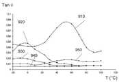
- 도 8 내지 도 10은 각각 Pd, tanδ, 및 유전율 εr의 변화량을 구조체의 표면 온도에 따른 함수로 도시한 도면이다.8 to 10 show the variation of Pd , tan δ, and permittivity εr as a function of the surface temperature of the structure, respectively.
명확하게 설명하기 위해, 도시되어 있는 객체의 다양한 요소들을 모두 동일한 비율로 도시하지는 않았음을 밝혀둔다.For clarity, it is to be noted that the various elements of the illustrated object are not drawn to scale.
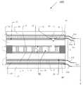
도 1은 두 개의 기판으로 형성되는 일부분(1)으로 구성되는 평면형 램프(1000)를 도시하며, 여기서 상기 기판은 예컨대 두께가 약 4 mm인 유리 시트(2,3)로 제조되고, 외부 주면(21,31)인 제1 면과 내부 주면(22,32)인 제2 면을 가지며, 상기 외부 주면은 바람직하게는 연속적이고 균질한 전도성 코팅부와 결합되고, 상기 전도성 코팅부는 전극(4,5)을 구성하며, 상기 내부 주면은, 예컨대 리튬 실리케이트를 기초로 하는 무기 매트릭스에서 분산되는 형광체 입자 형태와 같은 광발광체(6,7)의 코팅부로서, 예컨대 투명한 코팅부와 연결된다.1 shows a
상기 시트(2,3)는 내부 주면(22,32)인 제2 면과 서로 결합되고, 상기 제2 면은 서로 마주보고 밀봉 프릿(8)에 의해 서로 결합되는 광발광체(6,7)를 지지하며, 상기 유리 시트 사이의 간격은 상기 유리 시트 사이에 배치된 유리 스페이서(9)에 의해 (일반적으로 5mm 이하의 값으로) 정해진다. 여기서, 상기 간격은 약 0.3mm 내 지 5mm, 예컨대 0.4mm 내지 2mm일 수 있다.The
상기 스페이서(9)는 구형, 원기둥형, 또는 입방체형일 수 있고, 또는 또 다른 다각형, 예컨대 십자형 단면을 가질 수 있다. 상기 스페이서는 적어도 플라즈마 가스에 노출되는 측방 표면이 상기 형광체(6,7)와 동일하거나 또는 상이한 형광체로 코팅될 수 있다.The
내부 공간(10)으로 지칭되는 상기 유리 시트(2,3) 사이의 공간에는 선택적으로 네온 또는 헬륨과 혼합되는 크세논과 같은 희유 가스가 보통 대기압의 약 1/10에 해당하는 낮은 압력으로 존재한다.In the space between the
유리 시트(2,3)인 상기 기판의 외면(21,31)에는 각각 전극이 증착된다. 각 전극(4,5)은 예컨대 불소가 도핑된 주석 산화물 층일 수 있다.Electrodes are deposited on
변형예에 따르면, 각 전극은 상기 기판과 다양한 방식으로 결합될 수 있다. 예컨대, 전극은 전기 절연체를 지지하는 요소의 외면 또는 내면에 증착될 수 있고, 이 절연체를 지지하는 요소는 코팅부가 상기 기판의 외면(21,31)에 눌려지도록 상기 기판과 결합된다. 이 요소는 예컨대 EVA 또는 PVB 타입의 플라스틱 필름, 또는 예컨대 PET, PVB, 및 PU 필름과 같은 다수의 플라스틱 필름일 수 있다.According to a variant, each electrode can be combined with the substrate in various ways. For example, an electrode may be deposited on the outer or inner surface of the element supporting the electrical insulator, which element is coupled to the substrate such that the coating is pressed against the
각 전극은 플라스틱 필름에 통합되거나 또는 이후에 강화 유리를 형성하는 상기 기판에 통합되는 금속 그리드 형태일 수 있고, 또는 서로 평행한 와이어 형태일 수 있다.Each electrode may be in the form of a metal grid integrated into the plastic film or subsequently integrated into the substrate forming the tempered glass, or in the form of wires parallel to each other.
각 전극은 또한 제1 전기 절연체와 제2 전기 절연체 사이에 끼워질 수 있고, 이는 상기 기판(2,3)에 결합될 수 있다. 상기 전극은 예컨대 두 개의 플라스틱 시 트 사이에 삽입될 수 있다.Each electrode can also be sandwiched between a first electrical insulator and a second electrical insulator, which can be coupled to the
전기 절연체의 또 다른 결합형태는 아래와 같다. 제1 전기 절연체로 PVB 시트가 선택되고, 이는 전극을 지지하는 PET 시트와 같은 제2 전기 절연체를 결합하는데 사용되며, 상기 전극은 상기 PVB 시트와 PET 시트 사이에 위치된다.Another combination of electrical insulators is as follows. A PVB sheet is selected as the first electrical insulator, which is used to join a second electrical insulator, such as a PET sheet supporting the electrode, which is located between the PVB sheet and the PET sheet.
전극(4)은 가요성 심(11a)을 통해 예컨대 40kHz의 주파수 f0의 고주파 전력 공급원에 연결된다. 상기 전극(4)은 약 1kV의 전위 V0 및 주파수 f0에 놓인다.The
기판(2,3)의 두께(더 일반적으로는 전극을 분리하는 유전체의 두께)가 작을수록(예컨대 2mm 또는 1mm까지 감소), 전압 V0는 더 낮아져야 하므로, 절연성을 보장하기 위해서는 V 및 f에 대한 조건이 더 탄력적이어야 한다.The smaller the thickness of the
가요성 심(11b)을 통해 전력공급되는 전극(5)은 약 220V의 전위 V1 및 50Hz의 주파수 f1에 놓인다.
이 전극(4)의 상부에는 층간 유전체(14)와 보호 전도체(41)가 배치되고, 상기 보호 전도체는 가요성 심(11c)을 통해 전기가 공급되고 상기 전극(5)에 연결된다.On top of this
이 보호 전도체(41)는 예컨대 3.85mm의 두께로 유리 시트(16)의 내면에 전체적으로 증착되는 불소가 도핑된 주석 산화물의 층 형태일 수 있고, 또는 대안적으로 두꺼운 플라스틱 지지체에 증착될 수도 있다.This
전극(4)의 면적이 0.2m2이고 전력이 100W일 때, 3.85mm 두께의 유리 시 트(16)에 동일한 면적의 연속적인 금속체를 배치함으로써 측정되는 누설 전류는 약 0.6mA(피크값)이다.When the area of the
상기 유전체(14)는 예컨대 전극(5)에 배치되는 후술할 필름(15)과 동일한 하나 이상의 폴리머 필름과 같은 용량성의 적층 중간층이다. 표면 온도가 30℃이고, 주파수 f0가 40kHz이며, 전극(4)의 면적이 0.2m2이고, 전력 P가 100W일 때, 전력 Pd는 아래와 같다.The dielectric 14 is a capacitive laminated intermediate layer, such as, for example, one or more polymer films identical to the
- 필름(14)이 캐패시턴스 C를 제한하기 위해 두께가 5mm인 PVB, PU, 또는 PET 필름으로 구성되면 약 35W;About 35 W if the
- 필름(14)이 두께가 3.8mm인 EVA 필름이라면 약 18W;About 18 W if the
- 필름(14)이 두께가 1.6mm인 EVA 필름과 결합(PC의 부착력을 더 우수하게 하기 위함)되는 두께가 4mm인 PC 필름이라면 약 13W;About 13 W if the
- 필름(14)이 4mm의 공기로 대체된다면(이 경우에는 하나 이상의 스페이서 및/또는 주변 밀봉부를 사용함) 약 14W, 또는 상기 필름이 2mm의 공기(2mm의 공기는 9mm의 PVB와 등가) 및 3.15mm의 유리로 대체된다면 약 5W이다.About 14 W if the
이러한 조건하에서 유전율 εr은 아래와 같다.Under these conditions, the dielectric constant εr is
- 필름(14)이 두께가 5mm인 PVB 필름이라면 약 4;About 4 if the
- 필름(14)이 두께가 3.8mm인 EVA 필름이라면 약 3.5이다.If the
이러한 조건하에서 tanδ는 아래와 같다.Under these conditions tan δ is as follows.
- 필름(14)이 캐패시턴스 C를 제한하기 위해 두께가 5mm 이상인 PVB 필름으 로 구성되면 약 0.06;About 0.06 if the
- 필름(14)이 두께가 3.8mm인 EVA 필름이라면 약 0.018;About 0.018 if the
- 필름(14)이 두께가 1.6mm인 EVA 필름과 결합되는 두께가 4mm인 PC 필름이라면 약 0.008;About 0.008 if the
- 필름(14)이 4mm의 공기(2mm의 공기는 9mm의 PVB와 등가)로 대체된다면 약 0.005, 또는 상기 필름이 2mm의 공기 및 3.15mm의 유리로 대체된다면 약 0.012이다.About 0.005 if the
상기 층간 유전체(14)의 단자 사이의 전압 U는 V0 - V1이다.The voltage U between the terminals of the
상기 외면(31)의 바깥쪽에는 예컨대 두께 1.5mm의 PVB 또는 EVA로 제조되는 적절한 수지 또는 투명한 플라스틱 필름(15)이 배치되고, 상기 필름은 예컨대 두께 3.15mm의 유리 시트(17)와 같은 유리 기판에 적층되는 중간층 역할을 하며, 또는 대안적으로 두꺼운 경질 플라스틱 지지체에 적층될 수도 있다.Outside the
전극(5)의 면적이 0.2m2이고 전력이 100W일 때, 3.15mm 두께의 유리 시트(17) 위에 동일한 면적의 연속적인 금속체를 배치함으로써 측정되는 누설 전류는 약 0.65mA(피크값)이다.When the area of the
상기 금속체가 더 작은 면적을 갖는다면, 누설 전류도 비례하여 감소된다.If the metal body has a smaller area, the leakage current is also reduced proportionally.
안전성 향상과 관련된 제1 변형예에 따르면, V1은 램프에 대한 전력 공급원 회로의 한 지점에 제공되는 접지 전위에 놓이고, 이 경우 누설 전류는 0이다.According to a first variant relating to improved safety, V1 is at a ground potential provided at a point in the power supply circuit for the lamp, in which case the leakage current is zero.
안전성 향상과 관련된 제2 변형예에 따르면, 상기 전극(5)과 보호 전도 체(41)가 연결되지 않는다. 예컨대, 전도체(41)는 그대로 V1인 반면, 제2 전극은 220V/50Hz의 간선에 연결되거나 또는 접지에 연결된다.According to a second variant relating to the improvement of safety, the
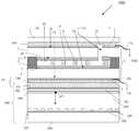
도 2에 도시된 실시예에서, 램프 구조체(2000)는 아래의 차이점을 제외하고는 기본적으로 도 1의 구조체와 동일하다.In the embodiment shown in FIG. 2, the
- 보호 전도체(42)는 강화 유리(161) 내의 그리드이고, 전극 상부의 유리 두께는 예컨대 약 3mm이다;The
- 전극(5)은 3.85mm의 유리(17)에 결합되는 필름으로서, 예컨대 PVB 또는 EVA 필름과 결합된 PET 필름에 배치된다;The
- 불투명한 광발광체(61,71)가 조명이 분화되도록 가장자리에만 배치된다.
또한, 상기 전극(5)과 전도체(42)는 접지에 연결된다. 상기 층간 유전체(14)는 주변 밀봉부(8') 사이에 두께가 2mm인 공기 또는 질소와 같은 가스층(141)과, 두께가 3mm인 유리층을 포함한다. 상기 층간 유전체(14)의 단자 사이의 전압 U는 V0이다.In addition, the
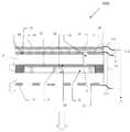
도 3에 도시된 실시예에서, 램프 구조체(3000)는 아래의 차이점을 제외하고는 기본적으로 도 1의 구조체와 동일하다.In the embodiment shown in FIG. 3, the
- 보호 전도체(43)는 층간 유전체(14)를 덮도록 배치되고, 이 전도체(43)는 또한 접착 필름에 의해, 예컨대 폴리우레탄 및 폴리카보네이트에 의해 보호될 수 있다;The
- 유전체(14)는 두께가 4mm인 PC 시트(143) 밑에 두께가 1.6mm인 EVA 시 트(142)를 포함한다;The dielectric 14 comprises an
- 유리로 적층되는 반대쪽 판이 없고, 전극(5) 위에 플라스틱 층간 필름이 없다.There is no opposite plate laminated with glass and there is no plastic interlayer film on the
상기 전극(5)과 전도체(43)는 접지에 연결되므로, 상기 전도체(43)는 스크린이 된다. 상기 층간 유전체(14)의 단자 사이의 전압 U는 V0이다.Since the
도 4에 도시된 실시예에서, 램프 구조체(4000)는 아래의 차이점을 제외하고는 기본적으로 도 1의 구조체와 동일하다. 즉, 50kHz의 주파수 f0에 대해, 전극(4)은 약 300V의 전위 V+에 놓이고 전극(5)은 약 700V의 반대 부호 전위 V-에 놓인다. 상기 구조체는 또한 연속적이고 투명한 전기 전도층 형태로 이루어지는 두 개의 보호 전도체(44,44')를 사용한다. 상기 두 개의 보호 전도체(44,44')는 누설 전류를 방지하기 위해 램프에 전력을 공급하는 회로의 접지에 연결된다.In the embodiment shown in FIG. 4, the
층간 유전체는 두 부분(14,14')에 형성되고, 이들은 예컨대 두께가 각각 2.5mm인 PVB 형태로 이루어지거나, 또는 상술한 다른 필름 변형예의 형태로 이루어진다. 소비 전력 Pd는 상기 두 부분(14,14')의 단자에서의 전력의 합과 일치한다. 상기 층간 유전체의 두 부분(14,14')의 단자에서의 전압 U는 V+ 및 V-이다.The interlayer dielectric is formed in the two
도 5에 도시된 실시예에서, 램프 구조체(5000)는 기본적으로 도 1의 구조체와 동일하다.In the embodiment shown in FIG. 5, the
전극(5)은 약 1kV의 전위 V0 및 40kHz 내지 50kHz의 고주파수 f0에 놓인다. 전극(4)은 약 220V의 전위 Vref 및 50kHz의 주파수 f에 놓이고, 적층 중간층(140)을 통해 적층된다.
전극(5) 밑에는 구조체의 안전성을 향상시키는 가역적인 전기화학 거울(100)이 배치된다.Beneath the
이 가역적인 전기화학 거울은,This reversible electrochemical mirror,
- EVA 필름(144) 및 PC 필름(101)으로 형성되는 층간 유전체(14);An
- 제1 전극(102);A first electrode 102;
- 예컨대 백금으로 제조되는 제1 핵생성부(103);A
- 예컨대 γ-부티롤락톤 솔벤트 내의 AgI 및 LiBr의 혼합물과 같은 전해질(104);
- 예컨대 백금으로 제조되는 제2 핵생성부(105);A
- 제2 전극(106);A
- 투명 기판, 바람직하게는 유리 시트(107), 또는 변형예로서 투명한 플라스틱 기판 또는 가요성 또는 경질의 복합 기판;A transparent substrate, preferably a
- 선택적으로, 저방사율 또는 태양광 제어층(108);을 차례대로 포함한다.Optionally, low emissivity or
상기 제1 핵생성부(103)는 서로 붙어있는 반면, 상기 제2 핵생성부(105)는 서로 떨어져 있다. 금속 소재, 바람직하게는 은의 원자 M+는 전착에 의해 상기 제1 핵생성부(103) 위에 반사면(109) 또는 반반사면(중간 상태)을 형성할 수 있고, 또는 상기 제2 핵생성부(105) 위에 전도성 섬 형태의 거의 투명한 표면(도시되지 않 음)을 형성할 수 있다.The
전압을 조절하거나 전류의 양을 측정하거나 또는 전기 저항을 측정함으로써 상기 반사면의 반사도 또는 레벨을 조절하는 수단(도시되지 않음)이 제공된다.Means (not shown) for adjusting the reflectivity or level of the reflective surface are provided by adjusting the voltage, measuring the amount of current, or measuring electrical resistance.
제1 전극(102) 또는 제2 전극(106)은 접지에 연결되므로(도시되지 않음), 전극(5) 측에서 누설 전류는 없다. 상기 층간 유전체(14)의 단자 사이의 전압 U는 V0 - Vref이다.Since the first electrode 102 or the
도 6에 도시된 실시예에서, 램프 구조체(6000)는 아래의 차이점을 제외하고 도 1의 구조체와 부분적으로 동일하다. 즉, 상기 램프 구조체는 UV 광원으로서 내부 공간(10) 내에 플라즈마 가스(6')를 가지며 단일 발광면(31)(발광은 넓은 화살표로 표시되어 있음)을 갖는 UV 램프(6000)이다.In the embodiment shown in FIG. 6, the
벽(2',3')은 UV가 투과되는 것으로 선택되므로, 벽(2')의 내면에는 예컨대 알루미나로 제조되는 UV 반사부(82)가 배치된다.Since the walls 2 ', 3' are selected to transmit UV, a
전극(5')은 UV 광선을 통과시키기 위해 스트립 형태(또는 와이어 및/또는 그리드 형태)로 이루어지며, 상기 전극은 코팅되지 않으므로 보호 전도체(45)처럼 접지에 연결된다. 상기 층간 유전체(14)의 단자 사이의 전압 U는 V0이다.The electrode 5 'is in the form of a strip (or wire and / or grid) to pass UV light, which is uncoated and therefore connected to ground as
도 7에 도시된 실시예에서, 램프 구조체(7000)는 아래의 차이점을 제외하고 도 1의 구조체와 부분적으로 동일하다. 즉, 상기 램프 구조체는 UV 광원으로서 내부 공간(10) 내에 플라즈마 가스(6')를 가지며 두 개의 발광면(발광은 두 개의 넓은 화살표로 표시되어 있음)을 갖는 UV 램프이다.In the embodiment shown in FIG. 7, the
벽(2',3')은 커버 유전체(162)와 같이 UV가 투과되는 것으로 선택된다. 보호 전도체(46)와 전극(4',5')은 UV 광선을 통과시키기 위해 예컨대 스트립 형태(또는 와이어 및/또는 그리드 형태)로 이루어지며, 층간 유전체(14)는 주변 밀봉부(8')를 가진 질소로 이루어진다. 상기 층간 유전체(14)의 단자 사이의 전압 U는 V0이다.The walls 2 ', 3' are selected such that UV is transmitted, such as the
전극(5')은 코팅되지 않으므로 보호 전도체(46)처럼 접지에 연결된다.The electrode 5 'is uncoated and therefore connected to ground like the
도 8 내지 도 10은 각각,8 to 10, respectively,
- 구조체(1000)의 표면 온도에 따른 Pd의 변화량(곡선(810 내지 850));The amount of change of Pd with the surface temperature of the structure 1000 (curves 810-850);
- 구조체(1000)의 표면 온도에 따른 tanδ의 변화량(곡선(910 내지 950));The amount of change of tanδ with the surface temperature of the structure 1000 (curves 910-950);
- 구조체(1000)의 표면 온도에 따른 유전율 εr의 변화량(곡선(1010 내지 1040));을 도시하며,The amount of change of the dielectric constant εr (
이는 아래와 같은 층간 유전체에 대한 것이다. 즉,This is for the interlayer dielectric as follows. In other words,
- 두께가 5mm인 PVB 층(곡선(810,910,1010));A PVB layer (
- 두께가 3.8mm인 EVA 층(곡선(820,920,1020));An EVA layer (
- 단일 PC 층(곡선(1030)), 또는 두께가 1.6mm인 EVA 층과 결합되는 두께가 4mm인 PC 층(곡선(830,930));A single PC layer (curve 1030) or a PC layer 4mm thick (curves 830,930) combined with an EVA layer 1.6 mm thick;
- 두께가 4mm인 단일 공기층(곡선(840,940,1040));A single air layer (
- 두께가 2mm인 공기층 및 3.15mm의 유리(곡선(850,950)).2 mm thick air layer and 3.15 mm glass (
EVA는 소비 전력 Pd가 100W 당 10W 내지 20W일 때 특히 30℃ 이상에서 PVB보다 더 양호한 거동을 제공함을 볼 수 있다.It can be seen that EVA provides better behavior than PVB, especially at 30 ° C. or higher when power consumption Pd is between 10W and 20W per 100W.
더욱 바람직한 EVA/PC 결합체는 소비 전력 Pd가 낮으며, 이는 온도에 따라 비교적 일정하다(100W 당 10W 내지 17W).More preferred EVA / PC combinations have a low power consumption Pd , which is relatively constant with temperature (10 to 17 W per 100 W).
전기적인 관점에서 보면, 공기 및 공기/유리 결합체도 소비 전력 Pd가 낮고(100W 당 5W 이하) 온도 안정성이 높아 바람직하다. 공기/유리 결합체는 손실각이 비교적 높지만, 캐패시턴스 값이 테스트된 절연체 중 가장 낮으므로 단자에서의 소비 전력이 낮다.From an electrical point of view, air and air / glass combinations are also preferred due to their low power consumption Pd (5 W or less per 100 W) and high temperature stability. The air / glass combination has a relatively high loss angle, but the power consumption at the terminals is low because the capacitance value is the lowest of the tested insulators.
상술한 예들은 본 발명을 제한하기 위한 것이 아니다.The above examples are not intended to limit the invention.
조립체의 비대칭적인 배치 및 대안적인 형태가 전극의 경우(소재의 선택, 형상의 선택, 유리 또는 플라스틱에 대한 배열의 선택 등) 및 보호 전도체의 경우(소재의 선택, 형상의 선택, 유리 또는 플라스틱에 대한 배열의 선택 등)에 이루어질 수 있고, 또는 층간 유전체의 경우(소재의 선택, 두께의 선택, 형상의 선택, 특히 연속적인 대부분의 영역 또는 천공되는 구성 또는 불연속적인 구성 등)에도 이루어질 수 있다.Asymmetrical arrangements and alternative forms of assembly can be found in the case of electrodes (selection of material, selection of shape, selection of arrangement for glass or plastic) and in the case of protective conductors (selection of material, choice of shape, glass or plastic). Selection of an array, etc.), or in the case of an interlayer dielectric (material selection, thickness selection, shape selection, in particular, most continuous areas or perforated or discontinuous configurations, etc.).
발광 구조체(1000 내지 5000)는 예컨대 이중 글레이징 유닛의 하나의 유리판에 대한 대체물로서 이중 글레이징 유닛의 전체 부분을 형성할 수 있다. 또한, 이러한 구성에서는 전도체가 이중 글레이징 유닛의 남아있는 유리판 위에 형성될 수 있다.The
플라즈마 가스에 의해 활성화되는 경우, 특정한 영역에서 분화되어 분포되는 광발광체로 인해 플라즈마의 에너지를 문제의 영역에서 가시 광선으로 전환할 수 있고, 이에 따라 발광 영역(광발광체의 특성에 따라 자체적으로 불투명하거나 투명함)을 구성할 수 있고 영구적으로 투명한 병치된 영역을 구성할 수 있다.When activated by the plasma gas, the photoluminescent material that is differentiated and distributed in a specific region can convert the energy of the plasma into visible light in the problematic region, and thus the luminescent region (which itself is opaque or Transparent) and permanently transparent juxtaposed areas.
상기 발광 영역은 기하학적 패턴(선, 점, 원, 정사각형, 또는 그 밖의 형상)의 어레이를 형성할 수도 있고, 패턴 사이의 간격 및/또는 패턴의 크기는 가변적일 수 있다.The light emitting regions may form an array of geometric patterns (lines, dots, circles, squares, or other shapes), and the spacing between the patterns and / or the size of the patterns may vary.
벽은 임의의 형상일 수 있다. 즉, 상기 벽의 외곽선은 특히 정사각형 또는 직사각형과 같은 오목하거나 볼록한 다각형일 수 있고, 특히 원형 또는 타원형과 같이 일정하거나 가변적인 곡률 반경으로 만곡될 수 있다.The wall can be of any shape. In other words, the outline of the wall may be a concave or convex polygon, in particular square or rectangular, and may be curved with a constant or variable radius of curvature, in particular circular or oval.
상기 벽은 평면형 또는 구부러진 형태일 수 있고, 바람직하게는 일정한 거리만큼 이격된다.The walls may be planar or curved and are preferably spaced apart by a certain distance.
상기 벽은 광학적 효과를 갖는 유리 기판, 특히 예컨대 착색되거나 장식되거나 구조화되거나 산란되는 벽일 수 있다.The wall may be a glass substrate having an optical effect, in particular a wall that is colored, decorated, structured or scattered, for example.
상기 구조체는 광물 수단(예컨대 유리 프릿)에 의해, 거의 투명한 소재(유리 등)에 의해, 또는 접착제(실리콘)로 밀봉될 수 있다.The structure may be sealed by mineral means (such as glass frit), by a substantially transparent material (such as glass), or with an adhesive (silicone).
Claims (16)
Translated fromKoreanApplications Claiming Priority (2)
| Application Number | Priority Date | Filing Date | Title |
|---|---|---|---|
| FR0653414AFR2905032A1 (en) | 2006-08-21 | 2006-08-21 | SENSITIVELY FLAT LUMINOUS AND / OR UV STRUCTURE |
| FR0653414 | 2006-08-21 |
Publications (1)
| Publication Number | Publication Date |
|---|---|
| KR20090042984Atrue KR20090042984A (en) | 2009-05-04 |
Family
ID=37719460
Family Applications (1)
| Application Number | Title | Priority Date | Filing Date |
|---|---|---|---|
| KR1020097005784ACeasedKR20090042984A (en) | 2006-08-21 | 2007-07-25 | Nearly flat visible light emission and / or light emitting structures |
Country Status (12)
| Country | Link |
|---|---|
| US (1) | US8120236B2 (en) |
| EP (1) | EP2070103B1 (en) |
| JP (1) | JP2010501975A (en) |
| KR (1) | KR20090042984A (en) |
| CN (1) | CN101785081B (en) |
| AT (1) | ATE500605T1 (en) |
| DE (1) | DE602007012911D1 (en) |
| ES (1) | ES2362446T3 (en) |
| FR (1) | FR2905032A1 (en) |
| PT (1) | PT2070103E (en) |
| TW (1) | TW200823956A (en) |
| WO (1) | WO2008023124A1 (en) |
Families Citing this family (138)
| Publication number | Priority date | Publication date | Assignee | Title |
|---|---|---|---|---|
| US7806543B2 (en) | 2007-01-03 | 2010-10-05 | Hill Phoenix, Inc. | Light system for a temperature controlled case |
| FR2915314B1 (en)* | 2007-04-17 | 2011-04-22 | Saint Gobain | UV FLOOR LAMP WITH DISCHARGES AND USES. |
| FR2915311B1 (en)* | 2007-04-17 | 2011-01-07 | Saint Gobain | FLASHLIGHT WITH DISCHARGE. |
| FR2936360B1 (en) | 2008-09-24 | 2011-04-01 | Saint Gobain | PROCESS FOR MANUFACTURING A MASK WITH SUBMILLIMETRIC OPENINGS FOR SUBMILLIMETRIC ELECTROCONDUCTIVE GRID, MASK AND SUBMILLIMETRIC ELECTROCONDUCTIVE GRID. |
| FR2936358B1 (en) | 2008-09-24 | 2011-01-21 | Saint Gobain | PROCESS FOR MANUFACTURING SUBMILLIMETRIC MOLDED MASKS FOR SUBMILLIMETRIC ELECTROCONDUCTIVE GRID, SUBMILLIMETRIC MOLDING MASK, SUBMILLIMETRIC ELECTROCONDUCTIVE GRID. |
| FR2936362B1 (en) | 2008-09-25 | 2010-09-10 | Saint Gobain | METHOD FOR MANUFACTURING AN ELECTROCONDUCTIVE SUBMILLIMETRIC GRID COATED WITH A SURGRILLE GRID, ELECTROCONDUCTIVE SUBMILLIMETER GRID COVERED WITH AN OVERGRILL |
| FR2939006B1 (en) | 2008-11-26 | 2010-11-12 | Saint Gobain | BALLAST PULSE FOR FLAT LAMPS |
| US8164818B2 (en) | 2010-11-08 | 2012-04-24 | Soladigm, Inc. | Electrochromic window fabrication methods |
| TWI442446B (en)* | 2011-04-19 | 2014-06-21 | Ind Tech Res Inst | Light-emitting element and display device |
| US12321075B2 (en) | 2011-12-12 | 2025-06-03 | View Operating Corporation | Electrochromic laminates |
| US10739658B2 (en) | 2011-12-12 | 2020-08-11 | View, Inc. | Electrochromic laminates |
| US8998469B1 (en) | 2013-01-08 | 2015-04-07 | Ruth M. Miller | Lighted ceramic tile assembly |
| CN103200290A (en)* | 2013-03-20 | 2013-07-10 | 上海鼎为软件技术有限公司 | Mobile terminal |
| US9905743B2 (en) | 2013-11-21 | 2018-02-27 | Ford Global Technologies, Llc | Printed LED heat sink double lock |
| US10064256B2 (en) | 2013-11-21 | 2018-08-28 | Ford Global Technologies, Llc | System and method for remote activation of vehicle lighting |
| US9868387B2 (en) | 2013-11-21 | 2018-01-16 | Ford Global Technologies, Llc | Photoluminescent printed LED molding |
| US9961745B2 (en) | 2013-11-21 | 2018-05-01 | Ford Global Technologies, Llc | Printed LED rylene dye welcome/farewell lighting |
| US9810401B2 (en) | 2013-11-21 | 2017-11-07 | Ford Global Technologies, Llc | Luminescent trim light assembly |
| US9809160B2 (en) | 2013-11-21 | 2017-11-07 | Ford Global Technologies, Llc | Tailgate illumination system |
| US9796325B2 (en) | 2013-11-21 | 2017-10-24 | Ford Global Technologies, Llc | Exterior light system for a vehicle |
| US9931991B2 (en) | 2013-11-21 | 2018-04-03 | Ford Global Technologies, Llc | Rotating garment hook |
| US10400978B2 (en) | 2013-11-21 | 2019-09-03 | Ford Global Technologies, Llc | Photoluminescent lighting apparatus for vehicles |
| US9821708B2 (en) | 2013-11-21 | 2017-11-21 | Ford Global Technologies, Llc | Illuminated exterior strip |
| US9849831B2 (en) | 2013-11-21 | 2017-12-26 | Ford Global Technologies, Llc | Printed LED storage compartment |
| US9950658B2 (en) | 2013-11-21 | 2018-04-24 | Ford Global Technologies, Llc | Privacy window system |
| US9797575B2 (en) | 2013-11-21 | 2017-10-24 | Ford Global Technologies, Llc | Light-producing assembly for a vehicle |
| US9902320B2 (en) | 2013-11-21 | 2018-02-27 | Ford Global Technologies, Llc | Photoluminescent color changing dome map lamp |
| US9839098B2 (en) | 2013-11-21 | 2017-12-05 | Ford Global Technologies, Llc | Light assembly operable as a dome lamp |
| US9796304B2 (en) | 2013-11-21 | 2017-10-24 | Ford Global Technologies, Llc | Vehicle floor lighting system having a pivotable base with light-producing assembly coupled to base |
| US10363867B2 (en) | 2013-11-21 | 2019-07-30 | Ford Global Technologies, Llc | Printed LED trim panel lamp |
| US10041650B2 (en) | 2013-11-21 | 2018-08-07 | Ford Global Technologies, Llc | Illuminated instrument panel storage compartment |
| US9989216B2 (en) | 2013-11-21 | 2018-06-05 | Ford Global Technologies, Llc | Interior exterior moving designs |
| US9539940B2 (en) | 2013-11-21 | 2017-01-10 | Ford Global Technologies, Llc | Illuminated indicator |
| US9969323B2 (en) | 2013-11-21 | 2018-05-15 | Ford Global Technologies, Llc | Vehicle lighting system employing a light strip |
| US9782504B2 (en)* | 2013-11-21 | 2017-10-10 | Ford Global Technologies, Inc. | Self-disinfecting surface with printed LEDs for a surface of a vehicle |
| RU2713535C2 (en)* | 2015-06-10 | 2020-02-05 | ФОРД ГЛОУБАЛ ТЕКНОЛОДЖИЗ, ЭлЭлСи | Self-insulating surface coating of vehicle |
| US10168039B2 (en) | 2015-08-10 | 2019-01-01 | Ford Global Technologies, Llc | Illuminated badge for a vehicle |
| US9889791B2 (en) | 2015-12-01 | 2018-02-13 | Ford Global Technologies, Llc | Illuminated badge for a vehicle |
| US10023100B2 (en) | 2015-12-14 | 2018-07-17 | Ford Global Technologies, Llc | Illuminated trim assembly |
| US10300843B2 (en) | 2016-01-12 | 2019-05-28 | Ford Global Technologies, Llc | Vehicle illumination assembly |
| US10501007B2 (en) | 2016-01-12 | 2019-12-10 | Ford Global Technologies, Llc | Fuel port illumination device |
| US10235911B2 (en) | 2016-01-12 | 2019-03-19 | Ford Global Technologies, Llc | Illuminating badge for a vehicle |
| US9855799B2 (en) | 2016-02-09 | 2018-01-02 | Ford Global Technologies, Llc | Fuel level indicator |
| US10011219B2 (en) | 2016-01-18 | 2018-07-03 | Ford Global Technologies, Llc | Illuminated badge |
| US9927114B2 (en) | 2016-01-21 | 2018-03-27 | Ford Global Technologies, Llc | Illumination apparatus utilizing conductive polymers |
| US9586519B1 (en) | 2016-01-27 | 2017-03-07 | Ford Global Technologies, Llc | Vehicle rear illumination |
| US10189401B2 (en) | 2016-02-09 | 2019-01-29 | Ford Global Technologies, Llc | Vehicle light strip with optical element |
| US9656598B1 (en) | 2016-02-23 | 2017-05-23 | Ford Global Technologies, Llc | Vehicle badge |
| US9751458B1 (en) | 2016-02-26 | 2017-09-05 | Ford Global Technologies, Llc | Vehicle illumination system |
| US10501025B2 (en) | 2016-03-04 | 2019-12-10 | Ford Global Technologies, Llc | Vehicle badge |
| US10118568B2 (en) | 2016-03-09 | 2018-11-06 | Ford Global Technologies, Llc | Vehicle badge having discretely illuminated portions |
| US9963001B2 (en) | 2016-03-24 | 2018-05-08 | Ford Global Technologies, Llc | Vehicle wheel illumination assembly using photoluminescent material |
| US10081296B2 (en) | 2016-04-06 | 2018-09-25 | Ford Global Technologies, Llc | Illuminated exterior strip with photoluminescent structure and retroreflective layer |
| US9902315B2 (en) | 2016-04-15 | 2018-02-27 | Ford Global Technologies, Llc | Photoluminescent lighting apparatus for vehicles |
| US9738219B1 (en) | 2016-05-11 | 2017-08-22 | Ford Global Technologies, Llc | Illuminated vehicle trim |
| US10064259B2 (en) | 2016-05-11 | 2018-08-28 | Ford Global Technologies, Llc | Illuminated vehicle badge |
| US10420189B2 (en) | 2016-05-11 | 2019-09-17 | Ford Global Technologies, Llc | Vehicle lighting assembly |
| US10631373B2 (en) | 2016-05-12 | 2020-04-21 | Ford Global Technologies, Llc | Heated windshield indicator |
| US9821710B1 (en) | 2016-05-12 | 2017-11-21 | Ford Global Technologies, Llc | Lighting apparatus for vehicle decklid |
| US9994144B2 (en) | 2016-05-23 | 2018-06-12 | Ford Global Technologies, Llc | Illuminated automotive glazings |
| US9896020B2 (en) | 2016-05-23 | 2018-02-20 | Ford Global Technologies, Llc | Vehicle lighting assembly |
| US9925917B2 (en) | 2016-05-26 | 2018-03-27 | Ford Global Technologies, Llc | Concealed lighting for vehicles |
| US9937855B2 (en) | 2016-06-02 | 2018-04-10 | Ford Global Technologies, Llc | Automotive window glazings |
| US9803822B1 (en) | 2016-06-03 | 2017-10-31 | Ford Global Technologies, Llc | Vehicle illumination assembly |
| US10343622B2 (en) | 2016-06-09 | 2019-07-09 | Ford Global Technologies, Llc | Interior and exterior iridescent vehicle appliques |
| US10205338B2 (en) | 2016-06-13 | 2019-02-12 | Ford Global Technologies, Llc | Illuminated vehicle charging assembly |
| US10131237B2 (en) | 2016-06-22 | 2018-11-20 | Ford Global Technologies, Llc | Illuminated vehicle charging system |
| US9855888B1 (en) | 2016-06-29 | 2018-01-02 | Ford Global Technologies, Llc | Photoluminescent vehicle appliques |
| US9840191B1 (en) | 2016-07-12 | 2017-12-12 | Ford Global Technologies, Llc | Vehicle lamp assembly |
| US9855797B1 (en) | 2016-07-13 | 2018-01-02 | Ford Global Technologies, Llc | Illuminated system for a vehicle |
| US9889801B2 (en) | 2016-07-14 | 2018-02-13 | Ford Global Technologies, Llc | Vehicle lighting assembly |
| US9840193B1 (en) | 2016-07-15 | 2017-12-12 | Ford Global Technologies, Llc | Vehicle lighting assembly |
| US9845047B1 (en) | 2016-08-08 | 2017-12-19 | Ford Global Technologies, Llc | Light system |
| US9827903B1 (en) | 2016-08-18 | 2017-11-28 | Ford Global Technologies, Llc | Illuminated trim panel |
| US10173604B2 (en) | 2016-08-24 | 2019-01-08 | Ford Global Technologies, Llc | Illuminated vehicle console |
| US10047659B2 (en) | 2016-08-31 | 2018-08-14 | Ford Global Technologies, Llc | Photoluminescent engine indicium |
| US10047911B2 (en) | 2016-08-31 | 2018-08-14 | Ford Global Technologies, Llc | Photoluminescent emission system |
| US10065555B2 (en) | 2016-09-08 | 2018-09-04 | Ford Global Technologies, Llc | Directional approach lighting |
| US10075013B2 (en) | 2016-09-08 | 2018-09-11 | Ford Global Technologies, Llc | Vehicle apparatus for charging photoluminescent utilities |
| US10308175B2 (en) | 2016-09-08 | 2019-06-04 | Ford Global Technologies, Llc | Illumination apparatus for vehicle accessory |
| US10043396B2 (en) | 2016-09-13 | 2018-08-07 | Ford Global Technologies, Llc | Passenger pickup system and method using autonomous shuttle vehicle |
| US9863171B1 (en) | 2016-09-28 | 2018-01-09 | Ford Global Technologies, Llc | Vehicle compartment |
| US10137829B2 (en) | 2016-10-06 | 2018-11-27 | Ford Global Technologies, Llc | Smart drop off lighting system |
| US10046688B2 (en) | 2016-10-06 | 2018-08-14 | Ford Global Technologies, Llc | Vehicle containing sales bins |
| US9914390B1 (en) | 2016-10-19 | 2018-03-13 | Ford Global Technologies, Llc | Vehicle shade assembly |
| US10086700B2 (en) | 2016-10-20 | 2018-10-02 | Ford Global Technologies, Llc | Illuminated switch |
| US9802534B1 (en) | 2016-10-21 | 2017-10-31 | Ford Global Technologies, Llc | Illuminated vehicle compartment |
| US10035473B2 (en) | 2016-11-04 | 2018-07-31 | Ford Global Technologies, Llc | Vehicle trim components |
| US9902314B1 (en) | 2016-11-17 | 2018-02-27 | Ford Global Technologies, Llc | Vehicle light system |
| US10220784B2 (en) | 2016-11-29 | 2019-03-05 | Ford Global Technologies, Llc | Luminescent windshield display |
| US9994089B1 (en) | 2016-11-29 | 2018-06-12 | Ford Global Technologies, Llc | Vehicle curtain |
| US10106074B2 (en) | 2016-12-07 | 2018-10-23 | Ford Global Technologies, Llc | Vehicle lamp system |
| US10118538B2 (en) | 2016-12-07 | 2018-11-06 | Ford Global Technologies, Llc | Illuminated rack |
| US10422501B2 (en) | 2016-12-14 | 2019-09-24 | Ford Global Technologies, Llc | Vehicle lighting assembly |
| US10144365B2 (en) | 2017-01-10 | 2018-12-04 | Ford Global Technologies, Llc | Vehicle badge |
| US9815402B1 (en) | 2017-01-16 | 2017-11-14 | Ford Global Technologies, Llc | Tailgate and cargo box illumination |
| US10173582B2 (en) | 2017-01-26 | 2019-01-08 | Ford Global Technologies, Llc | Light system |
| US10053006B1 (en) | 2017-01-31 | 2018-08-21 | Ford Global Technologies, Llc | Illuminated assembly |
| US9849830B1 (en) | 2017-02-01 | 2017-12-26 | Ford Global Technologies, Llc | Tailgate illumination |
| US9896023B1 (en) | 2017-02-09 | 2018-02-20 | Ford Global Technologies, Llc | Vehicle rear lighting assembly |
| US10427593B2 (en) | 2017-02-09 | 2019-10-01 | Ford Global Technologies, Llc | Vehicle light assembly |
| US9849829B1 (en) | 2017-03-02 | 2017-12-26 | Ford Global Technologies, Llc | Vehicle light system |
| US9758090B1 (en) | 2017-03-03 | 2017-09-12 | Ford Global Technologies, Llc | Interior side marker |
| US10240737B2 (en) | 2017-03-06 | 2019-03-26 | Ford Global Technologies, Llc | Vehicle light assembly |
| US10399483B2 (en) | 2017-03-08 | 2019-09-03 | Ford Global Technologies, Llc | Vehicle illumination assembly |
| US10150396B2 (en) | 2017-03-08 | 2018-12-11 | Ford Global Technologies, Llc | Vehicle cup holder assembly with photoluminescent accessory for increasing the number of available cup holders |
| US10195985B2 (en) | 2017-03-08 | 2019-02-05 | Ford Global Technologies, Llc | Vehicle light system |
| US10611298B2 (en) | 2017-03-13 | 2020-04-07 | Ford Global Technologies, Llc | Illuminated cargo carrier |
| US10166913B2 (en) | 2017-03-15 | 2019-01-01 | Ford Global Technologies, Llc | Side marker illumination |
| US10483678B2 (en) | 2017-03-29 | 2019-11-19 | Ford Global Technologies, Llc | Vehicle electrical connector |
| US10569696B2 (en) | 2017-04-03 | 2020-02-25 | Ford Global Technologies, Llc | Vehicle illuminated airflow control device |
| US10035463B1 (en) | 2017-05-10 | 2018-07-31 | Ford Global Technologies, Llc | Door retention system |
| US10399486B2 (en) | 2017-05-10 | 2019-09-03 | Ford Global Technologies, Llc | Vehicle door removal and storage |
| US9963066B1 (en) | 2017-05-15 | 2018-05-08 | Ford Global Technologies, Llc | Vehicle running board that provides light excitation |
| US10059238B1 (en) | 2017-05-30 | 2018-08-28 | Ford Global Technologies, Llc | Vehicle seating assembly |
| US10144337B1 (en) | 2017-06-02 | 2018-12-04 | Ford Global Technologies, Llc | Vehicle light assembly |
| US10493904B2 (en) | 2017-07-17 | 2019-12-03 | Ford Global Technologies, Llc | Vehicle light assembly |
| US10502690B2 (en) | 2017-07-18 | 2019-12-10 | Ford Global Technologies, Llc | Indicator system for vehicle wear components |
| US10137831B1 (en) | 2017-07-19 | 2018-11-27 | Ford Global Technologies, Llc | Vehicle seal assembly |
| US10160405B1 (en) | 2017-08-22 | 2018-12-25 | Ford Global Technologies, Llc | Vehicle decal assembly |
| US10186177B1 (en) | 2017-09-13 | 2019-01-22 | Ford Global Technologies, Llc | Vehicle windshield lighting assembly |
| US10137825B1 (en) | 2017-10-02 | 2018-11-27 | Ford Global Technologies, Llc | Vehicle lamp assembly |
| US10391943B2 (en) | 2017-10-09 | 2019-08-27 | Ford Global Technologies, Llc | Vehicle lamp assembly |
| US10207636B1 (en) | 2017-10-18 | 2019-02-19 | Ford Global Technologies, Llc | Seatbelt stowage assembly |
| US10189414B1 (en) | 2017-10-26 | 2019-01-29 | Ford Global Technologies, Llc | Vehicle storage assembly |
| US10723258B2 (en) | 2018-01-04 | 2020-07-28 | Ford Global Technologies, Llc | Vehicle lamp assembly |
| US10723257B2 (en) | 2018-02-14 | 2020-07-28 | Ford Global Technologies, Llc | Multi-color luminescent grille for a vehicle |
| US10627092B2 (en) | 2018-03-05 | 2020-04-21 | Ford Global Technologies, Llc | Vehicle grille assembly |
| US10281113B1 (en) | 2018-03-05 | 2019-05-07 | Ford Global Technologies, Llc | Vehicle grille |
| US10457196B1 (en) | 2018-04-11 | 2019-10-29 | Ford Global Technologies, Llc | Vehicle light assembly |
| US10703263B2 (en) | 2018-04-11 | 2020-07-07 | Ford Global Technologies, Llc | Vehicle light system |
| US10778223B2 (en) | 2018-04-23 | 2020-09-15 | Ford Global Technologies, Llc | Hidden switch assembly |
| US10576893B1 (en) | 2018-10-08 | 2020-03-03 | Ford Global Technologies, Llc | Vehicle light assembly |
| US10720551B1 (en) | 2019-01-03 | 2020-07-21 | Ford Global Technologies, Llc | Vehicle lamps |
| JP7484463B2 (en)* | 2020-06-12 | 2024-05-16 | 東芝ライテック株式会社 | Ultraviolet irradiation equipment |
| US20220152233A1 (en)* | 2020-11-19 | 2022-05-19 | Palo Alto Research Center Incorporated | Integrated uv disinfection |
| JPWO2022210251A1 (en)* | 2021-03-29 | 2022-10-06 | ||
| CN115692164A (en)* | 2022-10-21 | 2023-02-03 | 朗升光电科技(广东)有限公司 | Improved ultraviolet lamp |
Family Cites Families (15)
| Publication number | Priority date | Publication date | Assignee | Title |
|---|---|---|---|---|
| CH473354A (en)* | 1968-11-12 | 1969-05-31 | Sulzer Ernst | Anti-glare housing for lighting |
| US3999057A (en)* | 1975-03-03 | 1976-12-21 | Martin Hamacher | Lighting structure |
| JPH0212751A (en)* | 1988-06-30 | 1990-01-17 | Toshiba Lighting & Technol Corp | High-frequency lighting type fluorescent lamp |
| US5319282A (en)* | 1991-12-30 | 1994-06-07 | Winsor Mark D | Planar fluorescent and electroluminescent lamp having one or more chambers |
| JPH06349450A (en)* | 1993-06-08 | 1994-12-22 | Sony Corp | Planar phosphor tube |
| JPH07288102A (en)* | 1994-04-18 | 1995-10-31 | Nippon Sheet Glass Co Ltd | Flat-panel fluorescent lamp |
| US5702179A (en)* | 1995-10-02 | 1997-12-30 | Osram Sylvania, Inc. | Discharge lamp having light-transmissive conductive coating for RF containment and heating |
| JPH11143372A (en)* | 1997-11-07 | 1999-05-28 | Matsushita Electric Ind Co Ltd | Plasma display shield structure |
| US6340866B1 (en)* | 1998-02-05 | 2002-01-22 | Lg Electronics Inc. | Plasma display panel and driving method thereof |
| JP2002123182A (en)* | 2000-08-10 | 2002-04-26 | Nisshinbo Ind Inc | Front panel for plasma display panel and method of manufacturing the same |
| JP2003107463A (en)* | 2001-09-26 | 2003-04-09 | Hitachi Ltd | Liquid crystal display |
| JP3876170B2 (en)* | 2002-02-25 | 2007-01-31 | 松下電器産業株式会社 | Impact display film for flat display panel and flat display panel |
| FR2843483B1 (en)* | 2002-08-06 | 2005-07-08 | Saint Gobain | FLASHLIGHT, METHOD OF MANUFACTURE AND APPLICATION |
| JP2005302646A (en)* | 2004-04-15 | 2005-10-27 | Lecip Corp | Flat discharge tube illumination device |
| JP4583813B2 (en)* | 2004-06-03 | 2010-11-17 | Nec液晶テクノロジー株式会社 | Lamp unit and flat fluorescent lamp |
- 2006
- 2006-08-21FRFR0653414Apatent/FR2905032A1/ennot_activeWithdrawn
- 2007
- 2007-07-25DEDE602007012911Tpatent/DE602007012911D1/enactiveActive
- 2007-07-25KRKR1020097005784Apatent/KR20090042984A/ennot_activeCeased
- 2007-07-25ATAT07823636Tpatent/ATE500605T1/enactive
- 2007-07-25ESES07823636Tpatent/ES2362446T3/enactiveActive
- 2007-07-25USUS12/438,371patent/US8120236B2/ennot_activeExpired - Fee Related
- 2007-07-25PTPT07823636Tpatent/PT2070103E/enunknown
- 2007-07-25EPEP07823636Apatent/EP2070103B1/ennot_activeNot-in-force
- 2007-07-25JPJP2009525088Apatent/JP2010501975A/enactivePending
- 2007-07-25CNCN200780053652XApatent/CN101785081B/ennot_activeExpired - Fee Related
- 2007-07-25WOPCT/FR2007/051719patent/WO2008023124A1/enactiveApplication Filing
- 2007-08-02TWTW096128443Apatent/TW200823956A/enunknown
Also Published As
| Publication number | Publication date |
|---|---|
| CN101785081A (en) | 2010-07-21 |
| TW200823956A (en) | 2008-06-01 |
| ES2362446T3 (en) | 2011-07-05 |
| WO2008023124A1 (en) | 2008-02-28 |
| US8120236B2 (en) | 2012-02-21 |
| JP2010501975A (en) | 2010-01-21 |
| DE602007012911D1 (en) | 2011-04-14 |
| PT2070103E (en) | 2011-06-09 |
| ATE500605T1 (en) | 2011-03-15 |
| EP2070103B1 (en) | 2011-03-02 |
| US20090322202A1 (en) | 2009-12-31 |
| CN101785081B (en) | 2012-04-18 |
| FR2905032A1 (en) | 2008-02-22 |
| EP2070103A1 (en) | 2009-06-17 |
Similar Documents
| Publication | Publication Date | Title |
|---|---|---|
| US8120236B2 (en) | Light-emitting structure having leakage current limited by an electrical conductor with an adjustable frequency and an adjustable potential | |
| US8035289B2 (en) | Flat coplanar-discharge lamp and uses of same | |
| US20080143243A1 (en) | Planar or Substantially Planar Luminous Structure | |
| US20090179547A1 (en) | Flat uv lamp with coplanar discharge and uses thereof | |
| KR20100016640A (en) | Flat discharge lamp | |
| US20100253207A1 (en) | Flat uv discharge lamp, uses and manufacture | |
| JP2005535093A (en) | Flat lamp, manufacturing method and use | |
| US8169130B2 (en) | Planar or substantially planar luminous structure | |
| TW200912995A (en) | Flat discharge lamp | |
| US20100109506A1 (en) | Laminated flat lamp and its manufacturing process |
Legal Events
| Date | Code | Title | Description |
|---|---|---|---|
| PA0105 | International application | Patent event date:20090320 Patent event code:PA01051R01D Comment text:International Patent Application | |
| PG1501 | Laying open of application | ||
| A201 | Request for examination | ||
| PA0201 | Request for examination | Patent event code:PA02012R01D Patent event date:20120709 Comment text:Request for Examination of Application | |
| E902 | Notification of reason for refusal | ||
| PE0902 | Notice of grounds for rejection | Comment text:Notification of reason for refusal Patent event date:20131230 Patent event code:PE09021S01D | |
| E601 | Decision to refuse application | ||
| PE0601 | Decision on rejection of patent | Patent event date:20140326 Comment text:Decision to Refuse Application Patent event code:PE06012S01D Patent event date:20131230 Comment text:Notification of reason for refusal Patent event code:PE06011S01I |