KR20090034482A - Display device and manufacturing method thereof - Google Patents
Display device and manufacturing method thereofDownload PDFInfo
- Publication number
- KR20090034482A KR20090034482AKR1020070099704AKR20070099704AKR20090034482AKR 20090034482 AKR20090034482 AKR 20090034482AKR 1020070099704 AKR1020070099704 AKR 1020070099704AKR 20070099704 AKR20070099704 AKR 20070099704AKR 20090034482 AKR20090034482 AKR 20090034482A
- Authority
- KR
- South Korea
- Prior art keywords
- sensing
- forming
- sensing electrodes
- substrate
- display device
- Prior art date
- Legal status (The legal status is an assumption and is not a legal conclusion. Google has not performed a legal analysis and makes no representation as to the accuracy of the status listed.)
- Withdrawn
Links
Images


Classifications
- G—PHYSICS
- G02—OPTICS
- G02F—OPTICAL DEVICES OR ARRANGEMENTS FOR THE CONTROL OF LIGHT BY MODIFICATION OF THE OPTICAL PROPERTIES OF THE MEDIA OF THE ELEMENTS INVOLVED THEREIN; NON-LINEAR OPTICS; FREQUENCY-CHANGING OF LIGHT; OPTICAL LOGIC ELEMENTS; OPTICAL ANALOGUE/DIGITAL CONVERTERS
- G02F1/00—Devices or arrangements for the control of the intensity, colour, phase, polarisation or direction of light arriving from an independent light source, e.g. switching, gating or modulating; Non-linear optics
- G02F1/01—Devices or arrangements for the control of the intensity, colour, phase, polarisation or direction of light arriving from an independent light source, e.g. switching, gating or modulating; Non-linear optics for the control of the intensity, phase, polarisation or colour
- G02F1/13—Devices or arrangements for the control of the intensity, colour, phase, polarisation or direction of light arriving from an independent light source, e.g. switching, gating or modulating; Non-linear optics for the control of the intensity, phase, polarisation or colour based on liquid crystals, e.g. single liquid crystal display cells
- G02F1/133—Constructional arrangements; Operation of liquid crystal cells; Circuit arrangements
- G02F1/1333—Constructional arrangements; Manufacturing methods
- G02F1/13338—Input devices, e.g. touch panels
- G—PHYSICS
- G02—OPTICS
- G02F—OPTICAL DEVICES OR ARRANGEMENTS FOR THE CONTROL OF LIGHT BY MODIFICATION OF THE OPTICAL PROPERTIES OF THE MEDIA OF THE ELEMENTS INVOLVED THEREIN; NON-LINEAR OPTICS; FREQUENCY-CHANGING OF LIGHT; OPTICAL LOGIC ELEMENTS; OPTICAL ANALOGUE/DIGITAL CONVERTERS
- G02F1/00—Devices or arrangements for the control of the intensity, colour, phase, polarisation or direction of light arriving from an independent light source, e.g. switching, gating or modulating; Non-linear optics
- G02F1/01—Devices or arrangements for the control of the intensity, colour, phase, polarisation or direction of light arriving from an independent light source, e.g. switching, gating or modulating; Non-linear optics for the control of the intensity, phase, polarisation or colour
- G02F1/13—Devices or arrangements for the control of the intensity, colour, phase, polarisation or direction of light arriving from an independent light source, e.g. switching, gating or modulating; Non-linear optics for the control of the intensity, phase, polarisation or colour based on liquid crystals, e.g. single liquid crystal display cells
- G02F1/133—Constructional arrangements; Operation of liquid crystal cells; Circuit arrangements
- G02F1/1333—Constructional arrangements; Manufacturing methods
- G02F1/1339—Gaskets; Spacers; Sealing of cells
- G02F1/13394—Gaskets; Spacers; Sealing of cells spacers regularly patterned on the cell subtrate, e.g. walls, pillars
- G—PHYSICS
- G02—OPTICS
- G02F—OPTICAL DEVICES OR ARRANGEMENTS FOR THE CONTROL OF LIGHT BY MODIFICATION OF THE OPTICAL PROPERTIES OF THE MEDIA OF THE ELEMENTS INVOLVED THEREIN; NON-LINEAR OPTICS; FREQUENCY-CHANGING OF LIGHT; OPTICAL LOGIC ELEMENTS; OPTICAL ANALOGUE/DIGITAL CONVERTERS
- G02F2202/00—Materials and properties
- G02F2202/16—Materials and properties conductive
Landscapes
- Physics & Mathematics (AREA)
- Nonlinear Science (AREA)
- Mathematical Physics (AREA)
- Chemical & Material Sciences (AREA)
- Crystallography & Structural Chemistry (AREA)
- General Physics & Mathematics (AREA)
- Optics & Photonics (AREA)
- Liquid Crystal (AREA)
Abstract
Translated fromKoreanDescription
Translated fromKorean본 발명은 표시 장치에 관한 것으로, 특히 터치 스크린 패널 기능이 내장된 표시 장치 및 그 제조 방법에 관한 것이다.The present invention relates to a display device, and more particularly, to a display device having a touch screen panel function and a method of manufacturing the same.
터치 스크린 패널은 키보드를 사용하지 않고 표시 장치에 의해 화면에 나타난 문자나 특정 위치에 사람의 손 또는 물체를 접촉시켜 그 위치를 파악하여 특정 처리를 할 수 있는 장치이다. 종래의 터치 스크린 패널은 표시 장치와 별도로 제작되어 표시 장치와 합착되기 때문에 표시 장치의 두께를 증가시키게 된다. 따라서, 두께를 증가시키지 않기 위해 표시 장치 제조시 터치 스크린 패널 기능을 내장하는 터치 스크린 패널 내장형 표시 장치가 제시되었다.A touch screen panel is a device that can detect a location of a person's hand or an object by touching a character or a specific location displayed on the screen by a display device without using a keyboard and perform a specific process. Since the conventional touch screen panel is manufactured separately from the display device and bonded to the display device, the thickness of the display device is increased. Accordingly, in order to not increase the thickness, a touch screen panel embedded display device having a touch screen panel function in manufacturing a display device has been proposed.
터치 스크린 패널 내장형 표시 장치는 박막 트랜지스터 및 화소 전극 등이 형성되는 하부 기판에 센싱 전극이 형성되고, 컬러 필터 및 공통 전극 등이 형성되는 상부 기판에 도전성 스페이서가 형성되어 도전성 스페이서와 센싱 전극이 가압에 의해 접촉하는 위치를 파악하게 된다.In the touch screen panel embedded display device, a sensing electrode is formed on a lower substrate on which a thin film transistor, a pixel electrode, and the like are formed, and a conductive spacer is formed on an upper substrate on which a color filter and a common electrode, etc., are formed. It will grasp the position where it contacts.
그런데, 상부 기판과 하부 기판은 합착될 때 약간의 틀어짐이 발생되고, 이러한 틀어짐에 의해 센싱 전극과 도전성 스페이서도 오정렬된다. 특히 도전성 스페이서는 센싱 전극과의 접촉면이 평탄하지 않고 실질적으로 곡면으로 형성되어 실질적인 접촉 면적이 줄어들게 된다. 따라서, 상부 기판과 하부 기판에 오정렬이 발생되면 센싱 전극과 도전성 스페이서가 제대로 접촉하지 못해 센싱 불량이 발생하게 된다.However, a slight distortion occurs when the upper substrate and the lower substrate are bonded to each other, and the sensing electrode and the conductive spacer are also misaligned by this distortion. In particular, the conductive spacer has a non-flat contact surface with the sensing electrode and is substantially curved, thereby reducing the substantial contact area. Therefore, if misalignment occurs in the upper substrate and the lower substrate, the sensing electrode and the conductive spacer may not be properly contacted, resulting in a sensing failure.
본 발명은 오정렬에 의한 센싱 전극과 도전성 스페이서의 센싱 불량을 방지할 수 있는 터치 스크린 패널 내장형 표시 장치 및 그 제조 방법을 제공한다.The present invention provides a touch screen panel-embedded display device and a method of manufacturing the same which can prevent the sensing failure of the sensing electrode and the conductive spacer due to misalignment.
본 발명은 도전성 스페이서의 접촉면이 센싱 전극에 따라 연장되도록 형성하여 센싱 전극과 도전성 스페이서의 센싱 불량을 방지할 수 있는 터치 패널 내장형 표시 장치 및 그 제조 방법을 제공한다.The present invention provides a touch panel embedded display device and a method of manufacturing the same, which are formed so that the contact surface of the conductive spacer extends along the sensing electrode, thereby preventing a sensing failure between the sensing electrode and the conductive spacer.
본 발명의 일 양태에 따른 표시 장치는 서로 대면하도록 배치된 하부 기판 및 상부 기판; 상기 하부 기판상에 서로 이격되어 형성된 제 1 및 제 2 센싱 전극; 및 상기 제 1 및 제 2 센싱 전극 각각에 대응되도록 상기 상부 기판 상에 형성된 도전성 스페이서를 포함한다.A display device according to an aspect of the present invention includes a lower substrate and an upper substrate disposed to face each other; First and second sensing electrodes spaced apart from each other on the lower substrate; And a conductive spacer formed on the upper substrate so as to correspond to each of the first and second sensing electrodes.
상기 하부 기판은, 상기 제 1 기판의 일 방향으로 형성된 제 1 센싱 라인; 및 상기 제 1 센싱 라인과 절연되어 교차 형성된 제 2 센싱 라인을 포함한다.The lower substrate may include a first sensing line formed in one direction of the first substrate; And a second sensing line insulated from and intersecting with the first sensing line.
상기 제 1 및 제 2 센싱 전극은 상기 제 1 및 제 2 센싱 라인에 각각 연결된다.The first and second sensing electrodes are connected to the first and second sensing lines, respectively.
상기 제 2 센싱 라인은 적어도 하나의 단위 화소마다 형성된다.The second sensing line is formed for at least one unit pixel.
상기 도전성 스페이서는 상기 제 1 및 제 2 센싱 전극 각각에 대응되는 영역으로부터 상기 제 1 및 제 2 센싱 전극의 외변에 대응되는 영역으로 확장되도록 형 성된다.The conductive spacer is formed to extend from a region corresponding to each of the first and second sensing electrodes to a region corresponding to outer sides of the first and second sensing electrodes.
상기 도전성 스페이서는 상기 제 1 및 제 2 센싱 전극 사이에 대응되는 부분에서 폭이 좁게 형성된다.The conductive spacer is formed to have a narrow width at a portion corresponding to the first and second sensing electrodes.
상기 도전성 스페이서는 상기 제 1 및 제 2 센싱 전극 외변의 가운데에 대응되는 영역에서 최대 폭으로 형성된다.The conductive spacer is formed to a maximum width in an area corresponding to the center of the outer edges of the first and second sensing electrodes.
상기 도전성 스페이서는 상기 제 1 및 제 2 센싱 전극의 중앙부에 대응되는 영역으로부터 상기 제 1 및 제 2 센싱 전극의 외변으로 확장되는 서로 이격된 단면을 갖는 스페이서를 포함한다.The conductive spacer includes a spacer having cross sections spaced apart from each other extending from an area corresponding to a central portion of the first and second sensing electrodes to outer sides of the first and second sensing electrodes.
상기 도전성 스페이서는 상기 제 1 및 제 2 센싱 전극의 중앙부에 대응되는 영역으로부터 상기 제 1 및 제 2 센싱 전극의 외변으로 확장되는 서로 이격된 두개의 스페이서를 포함한다.The conductive spacer may include two spacers spaced apart from each other extending from an area corresponding to a central portion of the first and second sensing electrodes to outer sides of the first and second sensing electrodes.
상기 도전성 스페이서는 적어도 하나의 단위 화소마다 형성되며, 블랙 매트릭스 상부에 형성된다.The conductive spacer is formed for at least one unit pixel, and is formed on the black matrix.
상기 제 1 및 제 2 센싱 전극은 그 일부가 확장되어 서로 교차되도록 형성된다.The first and second sensing electrodes are formed such that portions thereof extend to cross each other.
본 발명의 다른 양태에 따른 표시 장치의 제조 방법은 제 1 기판 상부에 일 방향 및 타 방향으로 각각 연장되며 서로 절연되는 제 1 및 제 2 센싱 라인을 형성하고, 상기 제 1 및 제 2 센싱 라인과 각각 연결되는 제 1 및 제 2 센싱 전극을 형성하는 단계; 제 2 기판 상부에 상기 제 1 및 제 2 센싱 전극 각각에 대응되는 영 역으로부터 확장된 도전성 스페이서를 형성하는 단계; 및 상기 제 1 및 제 2 기판 사이에 셀갭 스페이서를 형성한 후 액정층을 형성하는 단계를 포함한다.According to another aspect of the present invention, there is provided a method of manufacturing a display device, wherein first and second sensing lines which extend in one direction and another direction and are insulated from each other are formed on a first substrate, respectively, Forming first and second sensing electrodes that are respectively connected; Forming a conductive spacer on the second substrate, the conductive spacer extending from an area corresponding to each of the first and second sensing electrodes; And forming a liquid crystal layer after forming a cell gap spacer between the first and second substrates.
상기 제 1 및 제 2 센싱 전극을 형성하는 단계는, 상기 제 1 기판 상에 상기 일 방향으로 연장되는 복수의 게이트 라인 및 이와 이격된 상기 제 1 센싱 라인을 형성하는 단계; 상기 제 1 기판 상에 게이트 절연막을 형성한 후 상기 게이트 절연막 상부의 소정 영역에 활성층 및 오믹 콘택층을 형성하는 단계; 상기 게이트 절연막 상부에 상기 게이트 라인과 교차되는 방향으로 연장되는 복수의 데이터 라인 및 일 데이터 라인과 이격되는 상기 제 2 센싱 라인을 형성하는 단계; 상기 기판 상에 보호막을 형성한 후 소정 영역을 식각하여 복수의 콘택홀을 형성하는 단계; 및 상기 보호막 상부의 상기 게이트 라인 및 상기 데이터 라인이 교차되는 영역에 화소 전극을 형성하고, 상기 복수의 콘택홀을 통해 상기 제 1 및 제 2 센싱 라인과 연결되는 상기 센싱 전극을 형성하는 단계를 포함한다.The forming of the first and second sensing electrodes may include forming a plurality of gate lines extending in the one direction and the first sensing lines spaced apart from each other on the first substrate; Forming a gate insulating layer on the first substrate and then forming an active layer and an ohmic contact layer in a predetermined region above the gate insulating layer; Forming a plurality of data lines extending in a direction crossing the gate line and the second sensing line spaced apart from one data line on the gate insulating layer; Forming a plurality of contact holes by etching a predetermined region after forming a passivation layer on the substrate; And forming a pixel electrode in an area where the gate line and the data line cross the upper portion of the passivation layer, and forming the sensing electrode connected to the first and second sensing lines through the plurality of contact holes. do.
상기 도전성 스페이서를 형성하는 단계는, 상기 제 2 기판 상부의 소정 영역에 블랙 매트릭스를 형성하는 단계; 상기 제 2 기판 상에 상기 센싱 전극과 대응되는 영역에 상기 센싱 전극을 따라 연장된 돌출부를 형성한 후 컬러 필터를 형성하는 단계; 및 상기 제 2 기판 상에 도전층을 형성한 후 패터닝하여 공통 전극 및 도전성 스페이서를 형성하는 단계를 포함한다.The forming of the conductive spacer may include forming a black matrix on a predetermined region on the second substrate; Forming a color filter on the second substrate in a region corresponding to the sensing electrode and then forming a protrusion extending along the sensing electrode; And forming a conductive layer on the second substrate and patterning the conductive layer to form a common electrode and a conductive spacer.
상기 돌출부는 상기 제 1 및 제 2 센싱 전극 각각의 중앙부에 대응하는 영역을 노출시키는 마스크를 이용한 사진 및 식각 공정으로 형성한다.The protrusion is formed by a photolithography and an etching process using a mask that exposes a region corresponding to a central portion of each of the first and second sensing electrodes.
상기 돌출부는 서로 이격된 두개의 돌출부를 포함한다.The protrusions include two protrusions spaced apart from each other.
본 발명에 의하면, 도전성 스페이서의 접촉면이 서로 이격된 제 1 및 제 2 센싱 전극의 두 중앙부에 대응하는 영역으로부터 확장되도록 형성하여 센싱 전극과 도전성 스페이서의 접촉 면적을 증가시킴으로써 센싱 전극과 도전성 스페이서의 오정렬에 의한 센싱 불량을 방지할 수 있어 터치 감도를 향상시킬 수 있고, 표시 장치의 신뢰성을 향상시킬 수 있다.According to the present invention, the contact surfaces of the conductive spacers are formed to extend from regions corresponding to two center portions of the first and second sensing electrodes spaced apart from each other, thereby increasing the contact area between the sensing electrodes and the conductive spacers, thereby misaligning the sensing electrodes and the conductive spacers. It is possible to prevent the poor sensing by the touch sensitivity can be improved, and the reliability of the display device can be improved.
이하, 첨부된 도면을 참조하여 본 발명의 실시 예를 상세히 설명하기로 한다. 그러나, 본 발명은 이하에서 개시되는 실시 예에 한정되는 것이 아니라 서로 다른 다양한 형태로 구현될 것이며, 단지 본 실시 예들은 본 발명의 개시가 완전하도록 하며, 통상의 지식을 가진 자에게 발명의 범주를 완전하게 알려주기 위해 제공되는 것이다.Hereinafter, with reference to the accompanying drawings will be described an embodiment of the present invention; However, the present invention is not limited to the embodiments disclosed below, but may be implemented in various forms, and only the embodiments are intended to complete the disclosure of the present invention and to those skilled in the art. It is provided for complete information.
도 1은 본 발명의 일 실시 예에 따른 터치 패널 내장형 표시 장치의 개략적인 블록도이다.1 is a schematic block diagram of a touch panel embedded display device according to an exemplary embodiment.
도 1을 참조하면, 본 발명의 일 실시 예에 따른 표시 장치는 표시 패널(100), 패널 구동부(400), 터치 위치 검출부(500) 및 위치 결정부(600)를 포함한다.Referring to FIG. 1, a display device according to an exemplary embodiment includes a
표시 패널(100)은 박막 트랜지스터, 화소 전극, 센싱 전극 등이 형성된 하부 기판(200)과, 컬러 필터, 공통 전극, 도전성 스페이서 등이 형성된 상부 기판(300) 과, 하부 기판(200)과 하부 기판(300) 사이에 형성된 액정층(미도시)을 포함한다.The
하부 기판(200)에는 일 방향으로 연장된 복수의 게이트 라인(GL1 내지 GLn)과 타 방향으로 연장된 복수의 데이터 라인(DL1 내지 DLm)이 형성된다. 복수의 게이트 라인(GL1 내지 GLn)과 복수의 데이터 라인(DL1 내지 DLm)이 교차하는 영역마다 화소들이 형성된다. 또한, 화소들에는 각각 스위칭 소자인 박막 트랜지스터(T)와 화소 전극(280)이 형성된다. 박막 트랜지스터(T)는 게이트 전극, 소오스 전극 및 드레인 전극으로 구성되어 게이트 전극이 게이트 라인(GL)에 연결되고, 소오스 전극이 데이터 라인(DL)에 연결되며, 드레인 전극이 화소 전극(280)에 연결된다. 또한, 하부 기판(200)에는 터치 스크린 패널 기능을 수행하기 위한 복수의 제 1 센싱 라인(미도시) 및 복수의 제 2 센싱 라인(미도시)이 형성되고, 제 1 및 제 2 센싱 라인과 연결되는 복수의 센싱 전극(미도시)이 형성된다. 제 1 센싱 라인은 게이트 라인(GL)과 동일 방향으로 연장될 수 있고, 제 2 센싱 라인은 데이터 라인(DL)과 동일 방향으로 연장될 수 있으며, 서로 전기적으로 절연되어 교차한다. 여기서, 제 1 및 제 2 센싱 라인에는 소정 전위의 초기 구동 전압(Vid)이 인가되고, 제 1 및 제 2 센싱 라인은 터치 위치 검출부(500)에 연결된다. 또한, 제 1 및 제 2 센싱 라인은 적색(R), 녹색(G) 및 청색(B) 화소 각각마다 형성될 수 있고, 소정 개수의 화소마다 형성할 수도 있다. 예를들어, 제 1 및 제 2 센싱 라인은 적어도 단위 화소마다 형성될 수 있는데, 단위 화소는 예를들어 3개의 화소들로 구성될 수 있다.A plurality of gate lines GL1 to GLn extending in one direction and a plurality of data lines DL1 to DLm extending in the other direction are formed on the
상부 기판(300)은 컬러 필터, 공통 전극 등이 형성되고, 하부 기판(200)과 대향 배치되어 하부 기판(200)과 체결됨으로써 액정층(미도시)을 수용한다. 상부 기판(300)은 각각의 화소들에 대응하는 컬러 필터들이 형성된 컬러 필터 기판으로 형성할 수 있다. 그러나, 컬러 필터는 하부 기판(200) 상에 형성할 수도 있다. 또한, 상부 기판(300)에는 터치 스크린 패널 기능을 수행하기 위한 복수의 도전성 스페이서(미도시)가 형성된다. 도전성 스페이서는 상부에 인가되는 외부 압력에 의해 하부 기판(200) 상에 형성되는 센싱 전극과 전기적으로 접촉된다. 도전성 스페이서는 적색(R), 녹색(G) 및 청색(B) 화소 각각마다 하나씩 형성될 수 있고, 3개의 화소들마다 하나씩 형성될 수도 있다.The
하부 기판(200)에 형성되는 제 1 및 제 2 센싱 라인과 연결되도록 형성된 센싱 전극과 상부 기판(300)에 형성되는 도전성 스페이서가 외부 압력에 의해 전기적으로 접촉함에 따라 제 1 및 제 2 센싱 라인에 인가된 초기 구동 전압(Vid)의 전위 레벨이 변동되는 것을 이용하여 외부 압력이 인가되는 위치의 x축 및 y축 좌표를 판단한다.The sensing electrode formed to be connected to the first and second sensing lines formed on the
패널 구동부(400)는 타이밍 제어부(410), 전원 공급부(420), 계조 전압 발생부(430), 데이터 구동부(440) 및 게이트 구동부(450)를 포함한다.The
타이밍 제어부(410)는 표시 장치의 전반적인 동작을 제어한다. 타이밍 제어부(410)는 그래픽 컨트롤러(미도시)와 같은 호스트 시스템으로부터 R, G 및 B의 원시 데이터 신호(DATA_O)와 제 1 제어 신호(CNTL1)가 제공됨에 따라 표시 패널(100)에 영상을 표시하기 위한 제 1 데이터 신호(DATA1), 제 2 제어 신호(CNTL1), 제 3 제어 신호(CNTL3) 및 제 4 제어 신호(CNTL4)를 출력한다. 구체적으로, 제 1 제어 신호(CNTL1)는 메인 클록 신호(MCLK), 수평 동기 신호(HSYNC) 및 수직 동기 신호(VSYNC)를 포함한다. 제 2 제어 신호(CNTL2)는 데이터 구동부(420)를 제어하는 수평 시작 신호(STH), 반전 신호(REV) 및 데이터 로드 신호(TP)를 포함한다. 제 3 제어 신호(CNTL3)는 게이트 구동부(430)를 제어하는 개시 신호(STV), 클록 신호(CK) 및 출력 인에이블 신호(OE)등을 포함한다. 제 4 제어 신호(CNTL4)는 전원 공급부(450)를 제어하는 클록 신호(CLK) 및 반전 신호(REV)등을 포함한다. 또한, 타이밍 제어부(410)는 원시 데이터 신호(DATA_O)의 출력 타이밍이 제어된 R', G', B'의 제 1 데이터 신호(DATA1)를 데이터 구동부(440)로 제공한다. 그리고, 타이밍 제어부(410)는 터치 위치 검출부(500)를 제어하는 제 5 제어 신호(CNTL5)를 더 출력한다. 제 5 제어 신호(CNTL5)는 전원 공급부(420)에서 출력되는 초기 구동 전압(Vid)이 제 1 및 제 2 센싱 라인들에 제공되도록 제어하는 클록 신호를 포함한다.The
전원 공급부(420)는 타이밍 제어부(410)로부터 출력되는 제 4 제어 신호(CNTL4)에 응답하여 표시 패널(100)로 제공되는 공통 전압들(Vcom, Vcst), 터치 스크린 기능을 수행하기 위해 하부 기판(200)에 제공되는 초기 구동 전압(Vid), 계조 전압 발생부(430)로 제공되는 아날로그 구동 전압(AVDD) 및 게이트 구동부(450)로 제공되는 게이트 온/오프 전압(Von, Voff)등을 출력한다.The
계조 전압 발생부(430)는 전원 공급부(420)에서 제공되는 아날로그 구동 전압(AVDD)을 기준 전압으로 사용하여 감마 커브가 적용된 저항비를 갖는 분배 저항을 기초로 계조 레벨수에 대응하는 복수개의 기준 계조 전압(VGMA_R)을 출력한다.The
데이터 구동부(440)는 계조 전압 발생부(430)로부터 출력되는 기준 계조 전압(VGMA_R)에 기초하여 계조 전압(VGMA)을 생성한다. 또한, 데이터 구동부(440)는 타이밍 제어부(410)로부터 입력되는 제 2 제어 신호(CNTL2)와 계조 전압(VGMA)에 기초하여 라인 단위로 제공되는 디지털 형태의 제 1 데이터 신호(DATA1)를 데이터 신호로 변환하며, 데이터 신호의 출력 타이밍을 제어하여 데이터 라인들(DL1 내지 DLm)에 출력한다.The
게이트 구동부(450)는 타이밍 제어부(410)에서 출력되는 제 3 제어 신호(CNTL3)와 전원 공급부(420)에서 출력되는 게이트 온/오프 전압(Von. Voff)에 따라 게이트 신호를 생성하고, 게이트 라인들(GL1 내지 GLn)에 순차적으로 출력한다.The
터치 위치 검출부(500)는 외부 압력이 가해진 지점의 위치 좌표를 검출한다. 즉, 외부 압력에 의해 상부 기판(300)에 형성된 도전성 스페이서가 하부 기판(200)의 센싱 전극과 접촉하여 제 1 및 제 2 센싱 라인에 인가되는 초기 구동 전압(Vid)이 변동되는 것을 검출하여 x축 및 y축의 위치 좌표를 판단한다. 이를 위해, 터치 위치 검출부(500)는 제 1 및 제 2 센싱 라인에 제 5 제어 신호(CNTL5)에 따라 초기 구동 전압(Vid)을 제공하는 전압 공급 제어부(미도시)와, 제 1 및 제 2 센싱 라인 각각에서 초기 구동 전압(Vid)이 변동되는 것을 검출하여 각각 제 1 검출 신호(DS1) 및 제 2 검출 신호(DS2)를 출력하는 데이터 샘플링부(미도시)를 포함한다. 여기서, 터치 위치 검출부(500)는 데이터 구동부(440)에 형성될 수도 있다.The
위치 결정부(600)는 터치 위치 검출부(500)에서 출력되는 제 1 및 제 2 검출 신호(DS1 및 DS2)에 의해 판단된 각각의 x축 및 y축의 위치 좌표를 조합하여 외부 압력이 표시 패널(100)에 인가되는 위치를 판단한다.The
도 2는 본 발명의 일 실시 예에 따른 표시 패널의 개략 평면도이고, 도 3 및 도 4는 도 2의 Ⅰ-Ⅰ' 라인 및 Ⅱ-Ⅱ' 라인을 따라 절취한 상태의 단면도로서, 본 실시 예는 3개의 화소마다 센싱 전극 및 도전성 스페이서가 형성되는 경우를 예로들어 설명한다.2 is a schematic plan view of a display panel according to an exemplary embodiment of the present invention, and FIGS. 3 and 4 are cross-sectional views of the display panel taken along lines II ′ and II-II ′ of FIG. 2. In the following description, a sensing electrode and a conductive spacer are formed for every three pixels.
도 2, 도 3 및 도 4를 참조하면, 본 발명의 일 실시 예에 터치 패널 내장형 표시 장치의 표시 패널(100)은 서로 대면하도록 배치된 하부 기판(200) 및 상부 기판(300), 하부 기판(200)과 상부 기판(300) 사이에 형성된 액정층(미도시)을 포함한다.2, 3, and 4, in an embodiment of the present invention, the
하부 기판(200)은 제 1 절연 기판(210) 상부에 일 방향으로 연장되는 복수의 게이트 라인(221)과, 게이트 라인(221)과 교차되어 연장된 복수의 데이터 라인(260)과, 게이트 라인(221)과 데이터 라인(260)에 의해 정의된 화소 영역에 형성된 화소 전극(280)과, 게이트 라인(221), 데이터 라인(260) 및 화소 전극(280)에 접속된 박막 트랜지스터(T)를 포함한다. 또한, 게이트 라인(221)과 이격되어 일 방향으로 연장된 제 1 센싱 라인(SL1)과, 데이터 라인(160)과 이격되어 타 방향으로 연장된 제 2 센싱 라인(SL2)과, 제 1 센싱 라인(SL1)과 연결된 제 1 센싱 전극(291)과, 제 2 센싱 라인(SL2)과 연결된 제 2 센싱 전극(292)를 더 포함한다.The
게이트 라인(221)은 예를들어 가로 방향으로 연장되어 형성되며, 게이트 라인(221)의 일부가 돌출되어 게이트 전극(222)이 형성된다. 게이트 라인(221)을 포 함한 전체 상부에 게이트 절연막(230)이 형성된다. 게이트 절연막(230)은 산화 실리콘(SiO2) 또는 질화 실리콘(SiNx) 등을 이용하여 단일층 또는 다층으로 형성될 수 있다.For example, the
게이트 전극(222) 상부의 게이트 절연막(230) 상부에는 비정질 실리콘 등의 반도체로 이루어진 활성층(241)이 각각 형성되며, 활성층(241)의 상부에는 실리사이드 또는 n형 불순물이 고농도로 도핑되어 있는 n+ 수소화 비정질 실리콘 등의 반도체로 이루어진 오믹 콘택층(251)이 형성된다. 오믹 콘택층(251)은 각각 소오스 전극(261)과 드레인 전극(262) 사이의 채널부에서는 제거될 수 있다.An
게이트 절연막(230) 상부에는 데이터 라인(260)이 형성된다. 데이터 라인(260)은 게이트 라인(221)과 교차되는 방향, 즉 세로 방향으로 연장 형성되며, 데이터 라인(260)이 게이트 라인(221)과 교차되는 영역이 화소 영역으로 정의된다. 데이터 라인(260)으로부터 오믹 콘택층(251) 상부까지 연장 돌출되어 소오스 전극(261)이 형성된다. 소오스 전극(261)과 이격되어 오믹 콘택층(251) 상부에 드레인 전극(262)이 형성된다.The
게이트 라인(221), 데이터 라인(260)을 포함한 전체 상부에 보호막(270)이 형성된다. 보호막(270)은 무기 절연막 또는 유기 절연막 등으로 형성될 수 있다. 또한, 보호막(270)의 소정 영역에는 드레인 전극(262)의 소정 영역을 노출시키는 제 1 콘택홀(271)과 제 1 센싱 라인(SL1)의 일부를 노출시키는 제 2 콘택홀(272)과 제 2 센싱 라인(SL2)의 일부를 노출시키는 제 3 콘택홀(273)이 형성된다.The
보호막(270) 상부에는 화소 전극(280)이 형성된다. 화소 전극(280)은 ITO(indium tin oxide) 또는 IZO(indium zinc oxide)등의 투명한 도전 물질로 형성된다. 화소 전극(280)은 제 1 콘택홀(271)을 통해 드레인 전극(262)과 연결된다.The
제 1 센싱 라인(SL1)은 게이트 라인(221)과 소정 간격 이격되어 형성되며, 게이트 라인(221)과 동시에 형성될 수 있다. 또한, 제 1 센싱 라인(SL1)로부터 분기된 브랜치 라인(BR)이 제 2 센싱 라인(SL2)과 소정 간격 이격되어 제 2 센싱 라인(SL2) 방향으로 형성될 수 있다. 그러나, 브랜치 라인(BR)은 연장 형성되지 않고 제 1 센싱 전극(191)과 연결되는 부분까지만 형성된다.The first sensing line SL1 may be formed to be spaced apart from the
제 2 센싱 라인(SL2)은 데이터 라인(260)과 소정 간격 이격되어 형성되는데, 소정 갯수의 화소마다 하나의 제 2 센싱 라인(SL2)이 형성된다. 예를들어 제 2 센싱 라인(SL2)은 청색 화소와 적색 화소 사이에 형성될 수 있다. 또한, 제 2 센싱 라인(SL2)은 데이터 라인(260)과 동시에 형성될 수 있다.The second sensing line SL2 is formed spaced apart from the
제 1 센싱 전극(291)은 제 2 콘택홀(272)을 통해 제 1 센싱 라인(SL1)의 브랜치 라인(BR)과 연결되도록 형성되며, 제 2 센싱 전극(292)는 제 3 콘택홀(273)을 통해 제 2 센싱 라인(SL2)과 연결되도록 형성된다. 또한, 제 1 및 제 2 센싱 전극(291 및 292)은 화소 전극(280) 형성시 화소 전극(280)과 이격되어 동시에 형성될 수 있으며, 서로 소정 간격 이격되어 형성된다.The
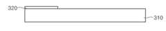
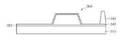
또한, 상부 기판(300)은 제 2 절연 기판(310) 상에 형성된 블랙 매트릭스(320)와, 컬러 필터(330)와, 공통 전극(340)을 포함한다. 또한, 셀갭 스페이 서(350) 및 도전성 스페이서(360)를 더 포함한다.In addition, the
블랙 매트릭스(320)는 서브 픽셀 이외의 영역, 예를들어 하부 기판(200)의 게이트 라인(221), 데이터 라인(260), 박막 트랜지스터(T), 제 1 및 제 2 센싱 라인(SL1 및 SL2)에 대응되는 상부 기판(300) 상에 형성되며, 화소 영역 이외의 영역으로 빛이 새는 것과 인접한 화소 영역들 사이의 광 간섭을 방지한다. 또한, 블랙 매트릭스(320)는 검은색 안료가 첨가된 감광성 유기 물질로 이루어진다. 검은색 안료로는 카본 블랙이나 티타늄 옥사이드 등을 이용한다.The
컬러 필터(330)는 블랙 매트릭스(320)를 경계로 하여 적색(R), 녹색(G) 및 청색(B) 필터가 반복되어 형성된다. 컬러 필터(330)는 광원으로부터 조사되어 액정층(미도시)을 통과한 빛에 색상을 부여하는 역할을 하며, 감광성 유기 물질로 형성될 수 있다.The
공통 전극(340)은 ITO(indium tin oxide) 또는 IZO(indium zinc oxide)등의 투명한 도전 물질로 형성되며, 블랙 매트릭스(320) 및 컬러 필터(330)를 포함한 절연 기판(310) 상부에 형성된다.The
한편, 셀갭 스페이서(350)는 하부 기판(200)과 상부 기판(300) 사이의 간격을 유지하기 위해 형성된다. 셀갭 스페이서(350)는 하나의 화소 또는 소정 갯수의 화소 마다 하나씩 배치되는데, 예를들어 3개의 화소마다 하나씩 배치되며, 청색 컬러 필터(330)과 적색 컬러 필터(330) 사이의 블랙 매트릭스(320) 상부에 형성될 수도 있다.Meanwhile, the
도전성 스페이서(360)는 소정 갯수의 화소마다 하나씩 배치된다. 예를들어 청색 화소와 적색 화소 사이의 블랙 매트릭스(320) 상에 형성되며, 하부 기판(200)의 제 1 및 제 2 센싱 전극(291 및 292)에 대응되도록 형성된다. 또한, 본 발명에 따른 도전성 스페이서(360)은 제 1 및 제 2 센싱 전극(291 및 292) 각각의 중앙부에 대응되는 영역으로부터 제 1 및 제 2 센싱 전극(291 및 292)의 네변에 대응되는 영역으로 확장되어 형성된다. 또한, 도전성 스페이서(360)는 제 1 및 제 2 센싱 전극(291 및 292) 각각의 중앙부로부터 제 1 및 제 2 센싱 전극(291 및 292)을 이루는 네변의 가운데에 대응하는 영역으로 최대폭으로 형성된다. 따라서, 도전성 스페이서(360)은 제 1 및 제 2 센싱 전극(291 및 292) 사이에 대응되는 영역에서 폭이 좁고 제 1 및 제 2 센싱 전극(291 및 292)에 대응되는 쪽으로 폭이 넓어지도록 형성될 수 있고, 서로 이격된 두개의 스페이서가 제 1 및 제 2 센싱 전극(291 및 292) 각각의 중앙부와 대응되도록 형성되어 도전층에 의해 서로 연결될 수 있다. 이러한 도전성 스페이서(360)의 다양한 형상을 도 5(a) 및 도 5(b)에 도시하였다. 도 5(a)에 도시된 바와 같이 도전성 스페이서(360)은 제 1 및 제 2 센싱 전극(291 및 292) 사이의 영역에 대응되는 중앙부에서 폭이 좁고 제 1 및 제 2 센싱 전극(291 및 292) 쪽으로 확장될수록 폭이 넓어지다가 다시 좁아지는 마름모 형상으로 형성될 수 있고, 제 1 센싱 전극(291)의 상부 끝으로부터 제 2 센싱 전극(292)의 하부 끝까지 대응되도록 길게 연장된 직사각형 형상으로 형성될 수 있으며, 중앙부에서 폭이 좁고 제 1 및 제 2 센싱 전극(291 및 292) 쪽으로 확장될수록 넓어지는 원형으로 형성될 수 있다. 또한, 제 1 및 제 2 센싱 전극(291 및 292)과 마찬가지로 서로 이격된 두개의 도전성 스페이서로 형성될 경우 도 5(b)에 도시된 바와 같이 서로 이격된 두개의 마름모, 직사각형 및 원형 등으로 형성될 수 있다. 이러한 도전성 스페이서(360)는 예를들어 제 1 센싱 전극(291)의 중앙부에 대응하는 영역과 제 2 센싱 전극(292)의 중앙부에 대응하는 영역을 노출시키는 두개의 투광부를 갖는 마스크를 이용한 사진 및 식각 공정으로 형성한다. 또한, 도전성 스페이서(360)의 형태는 마스크 노광부의 형태, 기판과 마스크 사이의 거리등에 따라 다양한 형태로 형성될 수 있다.One
한편, 도전성 스페이서(360)의 단면 구조는 도 4에 도시된 바와 같이 제 1 센싱 전극(291)의 일 끝단에 대응하는 영역으로부터 제 2 센싱 전극(292)의 타 끝단에 대응하는 영역까지 동일 높이로 형성될 수 있고, 도 6에 도시된 바와 같이 제 1 및 제 2 센싱 전극(291 및 292)에 대응되는 영역이 제 1 및 제 2 센싱 전극(291 및 292) 사이에 대응되는 영역보다 낮게 형성될 수 있다.Meanwhile, the cross-sectional structure of the
상기한 바와 같이 제 1 및 제 2 센싱 전극(291 및 292)의 중앙부에 대응되는 영역으로부터 제 1 및 제 2 센싱 전극(291 및 292)의 외변에 대응되는 영역으로 확장되어 형성된 도전성 스페이서(360)는 제 1 및 제 2 센싱 전극(291 및 292)과 오정렬되더라고 센싱 불량이 발생되지 않는다. 즉, 도 7에 도시된 바와 같이 도전성 스페이서(360)가 제 1 및 제 2 센싱 전극(291 및 292)과 상측, 하측, 좌측 및 우측으로 오정렬되더라도 접촉되어 센싱 불량이 발생되지 않는다.As described above, the
도 8 내지 도 12은 본 발명의 일 실시 예에 따른 터치 스크린 패널 내장형 표시 장치의 하부 기판 제조 방법을 설명하기 위해 순서적으로 도시한 소자의 단면도로서, 각도의 (a)는 도 2의 Ⅰ-Ⅰ' 라인을 따라 절취한 상태의 공정 단면도이고, 각도의 (b)는 도 2의 Ⅱ-Ⅱ' 라인을 절취한 상태의 공정 단면도이다.8 to 12 are cross-sectional views sequentially illustrating devices for manufacturing a lower substrate of a display device with a touch screen panel according to an embodiment of the present invention, wherein angle (a) is shown in FIG. It is process sectional drawing of the state cut along the I 'line, and angle (b) is process sectional drawing of the state which cut the II-II' line of FIG.
도 8(a) 및 도 8(b)를 참조하면, 유리, 석영, 세라믹 또는 플라스틱 등의 절연성 투명 기판(210) 상부에 제 1 도전층을 형성한다. 그리고, 제 1 마스크를 이용한 사진 및 식각 공정으로 제 1 도전층을 패터닝한다. 이에 의해 소정 간격으로 일 방향으로 연장되는 복수의 게이트 라인(221)과 게이트 라인(221)으로부터 돌출된 게이트 전극(222)이 형성된다. 또한, 게이트 라인(221)과 소정 간격 이격되어 제 1 센싱 라인(SL1)이 형성되고, 제 1 센싱 라인(SL1)으로부터 분기된 브랜치 라인(BR)이 형성된다.Referring to FIGS. 8A and 8B, a first conductive layer is formed on an insulating
도 9(a) 및 도 9(b)를 참조하면, 기판(210) 전체 상부에 게이트 절연막(230), 제 1 반도체층 및 제 2 반도체층을 순차적으로 형성한다. 그리고, 제 2 마스크를 이용한 사진 및 식각 공정으로 제 2 반도체층 및 제 1 반도체층을 패터닝한다. 이에 의해 활성층(241) 및 오믹 콘택층(251)이 형성된다. 활성층(241) 및 오믹 콘택층(251)은 게이트 전극(222)을 덮도록 형성된다. 여기서, 게이트 절연막(230)은 산화 실리콘 또는 질화 실리콘을 포함하는 무기 절연 물질을 이용하여 형성하는 것이 바람직하다. 또한, 제 1 반도체층은 비정질 실리콘층을 이용할 수 있고, 제 2 반도체층은 실리사이드 또는 n형 불순물이 고농도로 도핑되어 있는 n+ 수소화 비정질 실리콘을 이용할 수 있다.Referring to FIGS. 9A and 9B, the
도 10(a) 및 도 10(b)을 참조하면, 기판(210) 전체 상부에 제 2 도전층을 형 성한 후 제 3 마스크를 이용한 사진 및 식각 공정으로 제 2 도전층을 패터닝한다. 이에 의해 소오스 전극(261) 및 드레인 전극(262)을 포함하며 게이트 라인(221)과 직교하는 방향으로 연장되는 데이터 라인(260)이 형성된다. 또한, 이와 동시에 데이터 라인(260)과 소정 간격 이격된 제 2 센싱 라인(SL2)이 형성되는데, 제 2 센싱 라인(SL2)은 예를들어 세개의 화소마다 하나씩 형성된다.Referring to FIGS. 10A and 10B, after forming the second conductive layer on the
도 11(a) 및 도 11(b)를 참조하면, 기판(210) 전체 상부에 보호막(270)을 형성한 후 제 4 마스크를 이용한 사진 및 식각 공정으로 보호막(270)의 일부를 식각한다. 이에 의해 드레인 전극(262)을 노출시키는 제 1 콘택홀(171), 제 1 센싱 라인(SL1)을 노출시키는 제 2 콘택홀(272) 및 제 2 센싱 라인(SL2)을 노출시키는 제 3 콘택홀(273)이 형성된다.Referring to FIGS. 11A and 11B, after forming the
도 12(a) 및 도 12(b)를 참조하면, 보호막(270) 상부에 제 3 도전층을 형성한 후 제 5 마스크를 이용한 사진 및 식각 공정으로 제 3 도전층을 패터닝한다. 이에 의해 화소 전극(270)과 제 1 및 제 2 센싱 전극(291 및 292)가 형성된다. 화소 전극(270)은 게이트 라인(221)과 데이터 라인(260)이 교차하는 영역으로 정의된 화소 영역에 형성되며, 제 1 콘택홀(271)을 통해 드레인 전극(262)과 연결된다. 또한, 제 1 및 제 2 센싱 전극(291 및 292)은 제 2 및 제 3 콘택홀(272 및 273)을 통해 제 1 및 제 2 센싱 라인(SL1 및 SL2)과 각각 전기적으로 연결되도록 형성되며, 서로 소정 간격 이격되어 형성된다. 제 1 및 제 2 센싱 전극(291 및 292)은 화소 영역 이외의 영역에 형성되므로 화소 전극(270)과 전기적으로 연결되지 않는다. 여기서, 제 3 도전층은 ITO 또는 IZO를 포함하는 투명 도전막을 이용하여 형성하는 것이 바람직하다.12A and 12B, after forming a third conductive layer on the
도 13 내지 도 18은 본 발명의 일 실시 예에 따른 터치 스크린 패널 내장형 표시 장치의 상부 기판 제조 방법을 설명하기 위해 순서적으로 도시한 소자의 단면도로서, 각도의 (a)는 도 2의 Ⅰ-Ⅰ' 라인을 따라 절취한 상태의 공정 단면도이고, 각도의 (b)는 도 2의 Ⅱ-Ⅱ' 라인을 절취한 상태의 공정 단면도이다.13 to 18 are cross-sectional views sequentially illustrating elements of a method of manufacturing an upper substrate of a display device with a touch screen panel according to an embodiment of the present invention. An angle (a) is shown in FIG. It is process sectional drawing of the state cut along the I 'line, and angle (b) is process sectional drawing of the state which cut the II-II' line of FIG.
도 13(a) 및 도 13(b)를 참조하면, 유리, 석영, 세라믹 또는 플라스틱 등의절연성 투명 기판(310)상의 소정 영역에 블랙 매트릭스(320)를 형성한다. 블랙 매트릭스(320)는 카본 블랙이나 티타늄 옥사이드 등의 검은색 안료가 첨가된 감광성 유기 물질을 투명 기판(310) 상부에 형성한 후 제 1 마스크를 이용한 노광 및 현상 공정으로 형성할 수 있다. 블랙 매트릭스(320)는 화소 영역 이외의 영역, 즉 하부 기판(200)의 게이트 라인(221), 데이터 라인(260), 제 1 및 제 2 센싱 라인(SL1 및 SL2)에 대응되는 영역에 형성된다. 블랙 매트릭스(320)는 컬러 필터를 분리하는 동시에 하부 기판(200)의 화소 전극(270)이 제어하지 못하는 영역의 액정 셀을 통과해 나오는 광을 차단하여 표시 장치의 콘트라스트비를 향상시킨다.Referring to FIGS. 13A and 13B, a
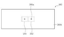
도 14(a) 및 도 14(b)를 참조하면, 블랙 매트릭스(320)가 형성된 기판(310) 상부에 절연막(360a)을 형성한다. 절연막(360a)은 유기 절연막 또는 무기 절연막을 이용하여 형성한다. 절연막(360a) 상부에 감광막(370)을 형성한 후 소정의 제 2 마스크(380)를 이용하여 노광 공정을 실시한다. 제 2 마스크(380)는 하부 기판(200)의 제 1 및 제 2 센싱 전극(291 및 292)에 대응되는 영역의 일부에 투광부(380a)가 형성된다. 바람직하게 제 2 마스크(380)는 도 19에 도시된 바와 같이 제 1 및 제 2 센싱 전극(291 및 292)의 중앙부에 대응되는 영역에 각각 투광부(380a)가 형성된다. 마스크(380)의 투광부(380a)를 통해 광이 입사되어 감광막(370)의 소정 영역이 노광된다. 그런데, 마스크(380)의 투광부(380a)의 형태 및 마스크(380)와 감광막(370) 사이의 거리 등에 따라 노광 영역(370a)을 다양하게 형성할 수 있다. 예를들어 마스크(380)와 감광막(370) 사이의 거리가 두 투광부(380a)를 통해 입사되는 광이 중첩되는 거리를 유지할 경우 마스크(380)의 두 투광부(380a) 사이에 해당되는 감광막(370) 영역도 노광된다. 따라서, 투광부(380a)의 형태에 따라 투광부(380a)가 마름모 형태로 형성될 경우 두 투광부(380a)의 중앙부에 대응하는 영역에서 폭이 좁고 양측으로 갈수록 폭이 넓어지다가 다시 좁아지는 마름모 형상으로 노광 영역(370a)이 형성될 수 있고, 감광막(370)의 일측으로부터 타측으로 길게 연장된 직사각형 형상으로 노광 영역(370a)이 형성될 수도 있으며, 두 투광부(380a) 사이의 중앙부에 대응하는 영역에서 폭이 좁고 양측으로 갈수록 넓어지는 원형으로 노광 영역(370a)이 형성될 수 있다. 또한, 마스크(380)와 감광막(370) 사이의 거리가 두 투광부(380a)를 통해 입사되는 광이 중첩되지 않는 거리를 유지할 경우 마스크(380)의 두 투광부(380a) 사이의 감광막(370)은 노광되지 않는다. 따라서, 투광부(380a)의 형태에 따라 서로 이격된 두개의 마름모, 직사각형 및 원형 등의 형태로 노광 영역(370a)이 형성된다.Referring to FIGS. 14A and 14B, an insulating
도 15(a) 및 도 15(b)를 참조하면, 감광막(370)을 현상하여 감광막(370)의 비노광 영역(370b)을 제거하고 노광 영역(370a)을 잔류시켜 감광막 패턴(370c)을 형성한다. 감광막 패턴(370c)을 마스크로 절연막(360)을 식각한다. 따라서, 블랙 매트릭스(320) 상부의 소정 영역에서 돌기부(360b)가 형성된다. 돌기부(360b)는 예를들어 세개의 화소당 하나씩 형성할 수 있다.Referring to FIGS. 15A and 15B, the
도 16(a) 및 도 16(b)를 참조하면, 감광막 패턴(370c)을 제거한 후 블랙 매트릭스(320) 및 돌기부(360b)가 형성된 기판(310) 상부에 다수의 컬러 필터(330), 예를들어 적색(R), 청색(B) 및 녹색(G) 컬러 필터를 형성한다. 컬러 필터(330)를 형성하는 공정을 살펴보면, 기판(310) 상부에 적색 성분의 안료가 분산된 네가티브 컬러 레지스트를 도포한 후 적색 컬러 필터가 형성될 영역을 개방하는 제 3 마스크를 이용하여 노광한다. 그리고, 현상액을 이용하여 네가티브 컬러 레지스트를 현상하면 노광된 영역은 제거되지 않고 패턴으로 남게 되며, 노광되지 않은 영역만이 제거된다. 따라서, 기판(310) 상에는 적색 컬러 필터(330)가 형성된다. 청색 컬러 필터 및 녹색 컬러 필터도 상기와 같은 과정을 통해 형성할 수 있다.Referring to FIGS. 16A and 16B, after removing the
도 17(a) 및 도 17(b)를 참조하면, 다수의 컬러 필터(330) 및 돌기부(360b)가 형성된 기판(310)의 전체 상부에 도전층을 형성한다. 도전층은 ITO 또는 IZO를 포함하는 투명 도전층을 이용하여 형성하며, 스퍼터링 등의 방법으로 형성한다. 이에 의해 공통 전극(340)이 기판(310) 전체면에 형성된다. 또한, 돌기부(360b) 상부에도 도전층이 형성됨으로써 도전성 스페이서(360)가 형성된다. 여기서, 공통 전극(340) 형성시 양호한 스텝 커버리지를 위하여 다수의 컬러 필터(230) 상부에 오버코트막이 형성될 수도 있다.Referring to FIGS. 17A and 17B, a conductive layer is formed on an entire upper portion of the
도 18(a) 및 도 18(b)를 참조하면, 기판(310) 전체 상부에 유기 물질을 형성 한 후 제 4 마스크를 이용한 사진 및 식각 공정을 실시한다. 이에 의해 셀갭 스페이서(350)가 형성된다. 이때, 셀갭 스페이서(350)는 블랙 매트릭스(220) 상에 형성된다.Referring to FIGS. 18A and 18B, after forming an organic material on the
한편, 상기 실시 예에서는 감광성이 없는 절연막(360a)을 이용하여 절연막(360a) 상부에 감광막(370)을 형성하였으나, 절연막(360a) 자체가 감광성을 가진 물질을 이용할 수 있고, 이 경우 감광막(370)을 형성하지 않고 절연막(360a)에 노광 공정을 실시할 수도 있다. 또한, 상기 실시 예에서는 돌기부(360b)를 먼저 형성한 후 컬러 필터(330)를 형성하였으나, 컬러 필터(330)를 먼저 형성한 후 돌기부(360b)를 형성할 수도 있다.Meanwhile, in the above embodiment, the
또한, 상기 실시 예에서는 셀갭 스페이서(350)가 상부 기판(300)상에 형성되는 것으로 설명하였으나, 셀갭 스페이서(350)는 하부 기판(200)상에 형성될 수 있다. 그리고, 상기 실시 예에서는 센싱 전극이 서로 이격된 제 1 및 제 2 센싱 전극(291 및 292)를 예로들어 설명하였으나, 센싱 전극은 이격되지 않고 단일 전극으로 형성될 수 있다. 또한, 제 1 및 제 2 센싱 전극(291 및 292)의 형상은 상기한 직사각형 형상 뿐만 아니라 제 1 및 제 2 센싱 전극(291 및 292)의 일부분이 서로 교차되도록 형성될 수 있다. 예를들어, 도 20에 도시된 바와 같이 제 1 및 제 2 센싱 전극(291 및 292)의 일부가 하부 및 상부로 각각 돌출되어 형성되고, 돌출된 부분이 서로 소정 간격 이격되어 마주보도록 형성될 수도 있다. 또한, 제 1 및 제 2 센싱 전극(291 및 292)이 각각 굴곡지게 형성되고, 굴곡진 부분이 서로 교차되도록 코일 형상으로 형성될 수 있다.In addition, in the above embodiment, the
도 1은 본 발명의 일 실시 예에 따른 표시 장치의 개략 블럭도.1 is a schematic block diagram of a display device according to an exemplary embodiment.
도 2는 본 발명의 일 실시 예에 따른 표시 장치의 표시 패널의 평면도.2 is a plan view of a display panel of a display device according to an exemplary embodiment.
도 3은 도 2의 Ⅰ-Ⅰ' 라인을 따라 절취한 상태의 단면도.3 is a cross-sectional view taken along the line II ′ of FIG. 2;
도 4는 도 2의 Ⅱ-Ⅱ' 라인을 따라 절취한 상태의 단면도.4 is a cross-sectional view taken along the line II-II ′ of FIG. 2.
도 5(a) 및 도 5(b)는 본 발명에 따른 도전성 스페이서의 변형 예에 따른 평면도.5 (a) and 5 (b) are plan views according to a modification of the conductive spacer according to the present invention.
도 6은 본 발명에 따른 도전성 스페이서의 단면 구조의 변형 예를 설명하기 위해 도 2의 Ⅱ-Ⅱ' 라인을 따라 절취한 상태의 단면도.6 is a cross-sectional view taken along the line II-II 'of FIG. 2 to illustrate a modification of the cross-sectional structure of the conductive spacer according to the present invention.
도 7은 본 발명에 따른 도전성 스페이서와 제 1 및 제 2 센싱 전극의 오정렬에 따른 접촉을 설명하기 위한 평면도.7 is a plan view for explaining the contact caused by the misalignment of the conductive spacer and the first and second sensing electrodes according to the present invention.
도 8 내지 도 12은 본 발명의 일 실시 예에 따른 표시 장치의 하부 기판의 제조 방법을 설명하기 위해 순서적으로 도시한 단면도.8 through 12 are cross-sectional views sequentially illustrating a method of manufacturing a lower substrate of a display device according to an exemplary embodiment.
도 13 내지 도 18은 본 발명의 일 실시 예에 따른 표시 장치의 상부 기판의 제조 방법을 설명하기 위해 순서적으로 도시한 단면도.13 to 18 are cross-sectional views sequentially illustrating a method of manufacturing an upper substrate of a display device according to an exemplary embodiment of the present invention.
도 19는 본 발명에 이용되는 마스크의 평면도.19 is a plan view of a mask used in the present invention.
도 20은 본 발명의 다른 실시 예에 따른 제 1 및 제 2 센싱 전극의 구성도.20 is a configuration diagram of a first and a second sensing electrode according to another embodiment of the present invention.
<도면의 주요 부분에 대한 부호의 설명><Explanation of symbols for the main parts of the drawings>
100 : 표시 패널200 : 하부 기판100: display panel 200: lower substrate
300 : 상부 기판400 : 패널 구동부300: upper substrate 400: panel driver
500 : 터치 위치 검출부600 : 위치 결정부500: touch position detection unit 600: position determination unit
360 : 도전성 스페이서291 및 292 : 제 1 및 제 2 센싱 전극360:
Claims (16)
Translated fromKoreanPriority Applications (2)
| Application Number | Priority Date | Filing Date | Title |
|---|---|---|---|
| KR1020070099704AKR20090034482A (en) | 2007-10-04 | 2007-10-04 | Display device and manufacturing method thereof |
| US12/187,250US20090091546A1 (en) | 2007-10-04 | 2008-08-06 | Display with touch screen panel and method of manufacturing the same |
Applications Claiming Priority (1)
| Application Number | Priority Date | Filing Date | Title |
|---|---|---|---|
| KR1020070099704AKR20090034482A (en) | 2007-10-04 | 2007-10-04 | Display device and manufacturing method thereof |
Publications (1)
| Publication Number | Publication Date |
|---|---|
| KR20090034482Atrue KR20090034482A (en) | 2009-04-08 |
Family
ID=40522859
Family Applications (1)
| Application Number | Title | Priority Date | Filing Date |
|---|---|---|---|
| KR1020070099704AWithdrawnKR20090034482A (en) | 2007-10-04 | 2007-10-04 | Display device and manufacturing method thereof |
Country Status (2)
| Country | Link |
|---|---|
| US (1) | US20090091546A1 (en) |
| KR (1) | KR20090034482A (en) |
Cited By (1)
| Publication number | Priority date | Publication date | Assignee | Title |
|---|---|---|---|---|
| US8624854B2 (en) | 2009-07-01 | 2014-01-07 | Casio Computer Co., Ltd. | Liquid crystal display panel and touch panel |
Families Citing this family (29)
| Publication number | Priority date | Publication date | Assignee | Title |
|---|---|---|---|---|
| KR101292765B1 (en)* | 2006-10-31 | 2013-08-02 | 삼성디스플레이 주식회사 | Display Apparatus and Method of Fabricating the Same |
| US7920129B2 (en) | 2007-01-03 | 2011-04-05 | Apple Inc. | Double-sided touch-sensitive panel with shield and drive combined layer |
| US20090174676A1 (en) | 2008-01-04 | 2009-07-09 | Apple Inc. | Motion component dominance factors for motion locking of touch sensor data |
| KR101500425B1 (en)* | 2008-08-27 | 2015-03-09 | 삼성디스플레이 주식회사 | Touch screen display apparatus |
| JP4930520B2 (en)* | 2009-01-26 | 2012-05-16 | ソニー株式会社 | Display device |
| JP4730443B2 (en)* | 2009-02-04 | 2011-07-20 | ソニー株式会社 | Display device |
| FR2949007B1 (en) | 2009-08-07 | 2012-06-08 | Nanotec Solution | DEVICE AND METHOD FOR CONTROL INTERFACE SENSITIVE TO A MOVEMENT OF A BODY OR OBJECT AND CONTROL EQUIPMENT INCORPORATING THIS DEVICE. |
| KR101588347B1 (en)* | 2009-09-28 | 2016-01-26 | 삼성디스플레이 주식회사 | Liquid crystal display panel, liquid crystal display device including same, and driving method of liquid crystal display device |
| TWI403791B (en)* | 2010-06-11 | 2013-08-01 | Au Optronics Corp | Touch display panel and touch sensor structure thereof |
| JP5657286B2 (en)* | 2010-06-25 | 2015-01-21 | 株式会社ジャパンディスプレイ | Liquid crystal display |
| US9563315B2 (en)* | 2010-11-09 | 2017-02-07 | Tpk Touch Solutions Inc. | Capacitive touch panel and method for producing the same |
| JP5755752B2 (en) | 2010-11-09 | 2015-07-29 | ティーピーケイ タッチ ソリューションズ インコーポレーテッド | Touch panel device |
| TWI469004B (en)* | 2011-04-08 | 2015-01-11 | Raydium Semiconductor Corp | Driving and sensing method for touch input device, and module using the same |
| TWI463626B (en)* | 2011-06-07 | 2014-12-01 | Novatek Microelectronics Corp | Touch panel and displaying apparatus |
| FR2976688B1 (en) | 2011-06-16 | 2021-04-23 | Nanotec Solution | DEVICE AND METHOD FOR GENERATING AN ELECTRICAL POWER SUPPLY IN AN ELECTRONIC SYSTEM WITH A VARIABLE REFERENCE POTENTIAL. |
| FR2985049B1 (en) | 2011-12-22 | 2014-01-31 | Nanotec Solution | CAPACITIVE MEASURING DEVICE WITH SWITCHED ELECTRODES FOR TOUCHLESS CONTACTLESS INTERFACES |
| US9336723B2 (en) | 2013-02-13 | 2016-05-10 | Apple Inc. | In-cell touch for LED |
| CN116560524B (en) | 2013-12-13 | 2024-10-01 | 苹果公司 | Integrated touch and display architecture for self-capacitance touch sensor |
| KR20150111546A (en)* | 2014-03-25 | 2015-10-06 | 삼성디스플레이 주식회사 | Display apparatus |
| US10133382B2 (en) | 2014-05-16 | 2018-11-20 | Apple Inc. | Structure for integrated touch screen |
| WO2015178920A1 (en) | 2014-05-22 | 2015-11-26 | Onamp Research Llc | Panel bootstrapping architectures for in-cell self-capacitance |
| WO2016072983A1 (en) | 2014-11-05 | 2016-05-12 | Onamp Research Llc | Common electrode driving and compensation for pixelated self-capacitance touch screen |
| US10795488B2 (en) | 2015-02-02 | 2020-10-06 | Apple Inc. | Flexible self-capacitance and mutual capacitance touch sensing system architecture |
| US10146359B2 (en) | 2015-04-28 | 2018-12-04 | Apple Inc. | Common electrode auto-compensation method |
| US10386962B1 (en) | 2015-08-03 | 2019-08-20 | Apple Inc. | Reducing touch node electrode coupling |
| EP3491500B1 (en) | 2016-07-29 | 2023-11-29 | Apple Inc. | Touch sensor panel with multi-power domain chip configuration |
| US10642418B2 (en) | 2017-04-20 | 2020-05-05 | Apple Inc. | Finger tracking in wet environment |
| CN108074962A (en)* | 2018-02-11 | 2018-05-25 | 京东方科技集团股份有限公司 | Array substrate and preparation method thereof, display panel, display device |
| US11662867B1 (en) | 2020-05-30 | 2023-05-30 | Apple Inc. | Hover detection on a touch sensor panel |
Family Cites Families (20)
| Publication number | Priority date | Publication date | Assignee | Title |
|---|---|---|---|---|
| US5463388A (en)* | 1993-01-29 | 1995-10-31 | At&T Ipm Corp. | Computer mouse or keyboard input device utilizing capacitive sensors |
| US5847690A (en)* | 1995-10-24 | 1998-12-08 | Lucent Technologies Inc. | Integrated liquid crystal display and digitizer having a black matrix layer adapted for sensing screen touch location |
| US6147680A (en)* | 1997-06-03 | 2000-11-14 | Koa T&T Corporation | Touchpad with interleaved traces |
| US5933102A (en)* | 1997-09-24 | 1999-08-03 | Tanisys Technology, Inc. | Capacitive sensitive switch method and system |
| US7663607B2 (en)* | 2004-05-06 | 2010-02-16 | Apple Inc. | Multipoint touchscreen |
| US6297811B1 (en)* | 1999-06-02 | 2001-10-02 | Elo Touchsystems, Inc. | Projective capacitive touchscreen |
| JP2001075074A (en)* | 1999-08-18 | 2001-03-23 | Internatl Business Mach Corp <Ibm> | Touch sensor type liquid crystal display device |
| US6847354B2 (en)* | 2000-03-23 | 2005-01-25 | The United States Of America As Represented By The Administrator Of The National Aeronautics And Space Administration | Three dimensional interactive display |
| WO2001095358A2 (en)* | 2000-05-22 | 2001-12-13 | Digit Wireless, Llc | Input devices and their use |
| JP3847083B2 (en)* | 2000-12-01 | 2006-11-15 | 富士通株式会社 | Touch panel device |
| JP3871547B2 (en)* | 2001-10-23 | 2007-01-24 | 富士通株式会社 | Touch panel device |
| US8514182B2 (en)* | 2001-12-27 | 2013-08-20 | Lg Display Co., Ltd. | Touch panel display device and method of fabricating the same |
| US7580030B2 (en)* | 2003-06-13 | 2009-08-25 | Semtech Corporation | Sensor for capacitive touch pad pointing device |
| US7388576B2 (en)* | 2005-02-23 | 2008-06-17 | Research In Motion Limited | Handheld electronic device and keypad providing enhanced usability and reduced size, and associated method |
| GB2428306B (en)* | 2005-07-08 | 2007-09-26 | Harald Philipp | Two-dimensional capacitive position sensor |
| DE202007005237U1 (en)* | 2006-04-25 | 2007-07-05 | Philipp, Harald, Southampton | Touch-sensitive position sensor for use in control panel, has bus bars arranged at distance to substrate, and detection region with units that are arranged at distance by non-conductive openings such that current flows into region |
| GB2437827B (en)* | 2006-05-05 | 2008-03-26 | Harald Philipp | Touch screen element |
| US8619054B2 (en)* | 2006-05-31 | 2013-12-31 | Atmel Corporation | Two dimensional position sensor |
| US20080204418A1 (en)* | 2007-02-27 | 2008-08-28 | Adam Cybart | Adaptable User Interface and Mechanism for a Portable Electronic Device |
| US20080303795A1 (en)* | 2007-06-08 | 2008-12-11 | Lowles Robert J | Haptic display for a handheld electronic device |
- 2007
- 2007-10-04KRKR1020070099704Apatent/KR20090034482A/ennot_activeWithdrawn
- 2008
- 2008-08-06USUS12/187,250patent/US20090091546A1/ennot_activeAbandoned
Cited By (1)
| Publication number | Priority date | Publication date | Assignee | Title |
|---|---|---|---|---|
| US8624854B2 (en) | 2009-07-01 | 2014-01-07 | Casio Computer Co., Ltd. | Liquid crystal display panel and touch panel |
Also Published As
| Publication number | Publication date |
|---|---|
| US20090091546A1 (en) | 2009-04-09 |
Similar Documents
| Publication | Publication Date | Title |
|---|---|---|
| KR20090034482A (en) | Display device and manufacturing method thereof | |
| KR101451938B1 (en) | Display panel with a built-in touch screen | |
| US10572062B2 (en) | Display device and touch detection method of display device | |
| US10437118B2 (en) | Liquid crystal display device and method for manufacturing the same | |
| US7675580B2 (en) | Liquid crystal display with built-in touch screen having particles for pressure concentration | |
| TWI492109B (en) | Touch panel substrate and electro-optical apparatus | |
| US8179482B2 (en) | Touch panel display and method of manufacturing the same | |
| US8477251B2 (en) | Display device and manufacturing method of the same | |
| KR101226440B1 (en) | Display panel and display device having the same and method of detecting touch position of the display device | |
| EP2357513B1 (en) | Liquid crystal display device and method of fabricating the same | |
| KR20160145121A (en) | Array substrate and manufacturing method and driving method therefor, and display device | |
| KR101305071B1 (en) | Array substrate and display panel having the same | |
| TW201310318A (en) | Touch panel substrate and electro-optical apparatus | |
| KR20090026576A (en) | Display device and manufacturing method thereof | |
| KR20140004887A (en) | Method for manufacturing liquid crystal display device | |
| KR102423865B1 (en) | Display device having touch sensor | |
| KR101885642B1 (en) | Liquid crystal display device and method for manufacturing the same | |
| US8581253B2 (en) | Display substrate and method of manufacturing the same | |
| US9029971B2 (en) | Display apparatus and method of manufacturing touch substrate | |
| KR102481182B1 (en) | Liquid display device | |
| KR101390400B1 (en) | Display and method of manufacturing the same | |
| KR20170065881A (en) | Display device with a built-in touch screen and method for fabricating the same | |
| US11137849B2 (en) | Touch display device and manufacturing method thereof | |
| KR20230133441A (en) | Display integrated touch sensing device | |
| KR101697272B1 (en) | Array Substrate for Liquid Crystal Display and Method for Fabricating The Same |
Legal Events
| Date | Code | Title | Description |
|---|---|---|---|
| PA0109 | Patent application | Patent event code:PA01091R01D Comment text:Patent Application Patent event date:20071004 | |
| PG1501 | Laying open of application | ||
| N231 | Notification of change of applicant | ||
| PN2301 | Change of applicant | Patent event date:20120913 Comment text:Notification of Change of Applicant Patent event code:PN23011R01D | |
| PC1203 | Withdrawal of no request for examination | ||
| WITN | Application deemed withdrawn, e.g. because no request for examination was filed or no examination fee was paid |