KR20090023052A - Tag antenna, and tag - Google Patents
Tag antenna, and tagDownload PDFInfo
- Publication number
- KR20090023052A KR20090023052AKR1020080056458AKR20080056458AKR20090023052AKR 20090023052 AKR20090023052 AKR 20090023052AKR 1020080056458 AKR1020080056458 AKR 1020080056458AKR 20080056458 AKR20080056458 AKR 20080056458AKR 20090023052 AKR20090023052 AKR 20090023052A
- Authority
- KR
- South Korea
- Prior art keywords
- antenna
- tag
- chip
- pattern
- spacer
- Prior art date
- Legal status (The legal status is an assumption and is not a legal conclusion. Google has not performed a legal analysis and makes no representation as to the accuracy of the status listed.)
- Granted
Links
Images


Classifications
- H—ELECTRICITY
- H01—ELECTRIC ELEMENTS
- H01Q—ANTENNAS, i.e. RADIO AERIALS
- H01Q1/00—Details of, or arrangements associated with, antennas
- H01Q1/12—Supports; Mounting means
- H01Q1/22—Supports; Mounting means by structural association with other equipment or articles
- H01Q1/2208—Supports; Mounting means by structural association with other equipment or articles associated with components used in interrogation type services, i.e. in systems for information exchange between an interrogator/reader and a tag/transponder, e.g. in Radio Frequency Identification [RFID] systems
- H01Q1/2225—Supports; Mounting means by structural association with other equipment or articles associated with components used in interrogation type services, i.e. in systems for information exchange between an interrogator/reader and a tag/transponder, e.g. in Radio Frequency Identification [RFID] systems used in active tags, i.e. provided with its own power source or in passive tags, i.e. deriving power from RF signal
- H—ELECTRICITY
- H01—ELECTRIC ELEMENTS
- H01Q—ANTENNAS, i.e. RADIO AERIALS
- H01Q1/00—Details of, or arrangements associated with, antennas
- H01Q1/36—Structural form of radiating elements, e.g. cone, spiral, umbrella; Particular materials used therewith
- H01Q1/38—Structural form of radiating elements, e.g. cone, spiral, umbrella; Particular materials used therewith formed by a conductive layer on an insulating support
- H—ELECTRICITY
- H01—ELECTRIC ELEMENTS
- H01Q—ANTENNAS, i.e. RADIO AERIALS
- H01Q13/00—Waveguide horns or mouths; Slot antennas; Leaky-waveguide antennas; Equivalent structures causing radiation along the transmission path of a guided wave
- H01Q13/10—Resonant slot antennas
- H01Q13/106—Microstrip slot antennas
- H—ELECTRICITY
- H01—ELECTRIC ELEMENTS
- H01Q—ANTENNAS, i.e. RADIO AERIALS
- H01Q9/00—Electrically-short antennas having dimensions not more than twice the operating wavelength and consisting of conductive active radiating elements
- H01Q9/04—Resonant antennas
- H01Q9/0407—Substantially flat resonant element parallel to ground plane, e.g. patch antenna
- H01Q9/045—Substantially flat resonant element parallel to ground plane, e.g. patch antenna with particular feeding means
- H—ELECTRICITY
- H01—ELECTRIC ELEMENTS
- H01Q—ANTENNAS, i.e. RADIO AERIALS
- H01Q9/00—Electrically-short antennas having dimensions not more than twice the operating wavelength and consisting of conductive active radiating elements
- H01Q9/04—Resonant antennas
- H01Q9/06—Details
- H01Q9/065—Microstrip dipole antennas
- H—ELECTRICITY
- H01—ELECTRIC ELEMENTS
- H01Q—ANTENNAS, i.e. RADIO AERIALS
- H01Q9/00—Electrically-short antennas having dimensions not more than twice the operating wavelength and consisting of conductive active radiating elements
- H01Q9/04—Resonant antennas
- H01Q9/16—Resonant antennas with feed intermediate between the extremities of the antenna, e.g. centre-fed dipole
- H01Q9/26—Resonant antennas with feed intermediate between the extremities of the antenna, e.g. centre-fed dipole with folded element or elements, the folded parts being spaced apart a small fraction of operating wavelength
- H—ELECTRICITY
- H01—ELECTRIC ELEMENTS
- H01Q—ANTENNAS, i.e. RADIO AERIALS
- H01Q9/00—Electrically-short antennas having dimensions not more than twice the operating wavelength and consisting of conductive active radiating elements
- H01Q9/04—Resonant antennas
- H01Q9/16—Resonant antennas with feed intermediate between the extremities of the antenna, e.g. centre-fed dipole
- H01Q9/28—Conical, cylindrical, cage, strip, gauze, or like elements having an extended radiating surface; Elements comprising two conical surfaces having collinear axes and adjacent apices and fed by two-conductor transmission lines
- H01Q9/285—Planar dipole
Landscapes
- Details Of Aerials (AREA)
- Waveguide Aerials (AREA)
- Aerials With Secondary Devices (AREA)
Abstract
Translated fromKoreanDescription
Translated fromKorean본 발명은 RFID 시스템에서의 태그, 즉 무선 IC 태그에 관한 것으로, 더욱 상세하게는 그러한 무선 IC 태그에 이용되는 태그 안테나와, 태그 안테나와 IC칩을 탑재한 태그에 관한 것이다.TECHNICAL FIELD The present invention relates to a tag in an RFID system, that is, a wireless IC tag, and more particularly, to a tag antenna used for such a wireless IC tag, and a tag on which a tag antenna and an IC chip are mounted.
RFID(라디오 프리퀀시 아이덴티피케이션) 시스템은, 물품의 관리 등에 광범위하게 이용되고 있다. 이 시스템은, 리더/라이터로부터 태그에 대하여 무선 전파를 날리고, 태그 내의 정보를 다시 리더//라이터에 태그로부터 전파를 돌려보냄으로써, 태그 내의 정보를 판독하는 것이다. 그 무선의 대역은 UHF대이며, 유럽에서는 868 MHz, 미국에서는 915 MHz, 일본에서는 953 MHz 부근의 주파수가 이용되고, 태그 내에 탑재되는 칩의 성능에도 따르지만, 통신 거리는 대략 3∼5 m이며, 리더/라이터의 출력은 1 W 정도이다.RFID (Radio Frequency Identification) systems are widely used for the management of articles and the like. The system reads the information in the tag by sending radio waves to the tag from the reader / writer and sending the information in the tag back to the reader / writer from the tag. The radio band is the UHF band, and frequencies around 868 MHz in Europe, 915 MHz in the United States, and 953 MHz in Japan are used, and depending on the performance of the chip mounted in the tag, the communication distance is approximately 3 to 5 m. The output of the writer is about 1 W.
이러한 무선 IC 태그의 안테나로서 다이폴 안테나를 사용하면, 양호한 지향성이 얻어지는 이점이 있지만, 안테나의 길이가 전파의 파장 λ의 1/2일 때에 안테나의 효율이 최대로 되기 때문에, 안테나의 길이가 길어지고, 결과적으로 태그를 소형화할 수 없다고 하는 문제점이 있었다. 또한, 이러한 다이폴 안테나를 이용하 는 경우에 안테나의 근방에 금속이 존재하면, 태그의 통신 거리가 격감하게 된다고 하는 문제점이 있었다.The use of a dipole antenna as an antenna of such a wireless IC tag has the advantage of obtaining good directivity, but the antenna length becomes longer because the efficiency of the antenna is maximized when the length of the antenna is 1/2 of the wavelength lambda of the radio wave. As a result, there is a problem that the tag cannot be miniaturized. In addition, in the case of using such a dipole antenna, if a metal is present in the vicinity of the antenna, there is a problem that the communication distance of the tag is reduced.
예를 들면, 금속에 접착하는 태그에 이용되는 안테나로서는, 종래부터 패치 안테나가 이용되고 있다. 도 14는, 그러한 패치 안테나 중 1개의 종래예의 설명도이다. 도 14에서 패치 안테나는, 패치 도체(100), 유전체(102)의 이면측의 그라운드 도체(101), 패치 도체(100)와 그라운드 도체(101) 사이에 끼워지는 유전체(102)에 의해 구성되고, IC칩은 패치 도체측의 칩 탑재부(103)에 탑재되고, 칩의 단자 전극의 한 쪽은 표면의 패치 도체(100)의 적절한 부분에 접속되고, 다른 쪽의 단자 전극은 쓰루홀(104)을 통하여 이면, 즉 그라운드 도체(101)에 접속된다.For example, a patch antenna is conventionally used as an antenna used for a tag attached to a metal. 14 is an explanatory diagram of one conventional example of such patch antennas. In FIG. 14, the patch antenna is composed of a
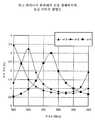
도 15는, 도 14의 패치 안테나의 통신 거리의 예를 도시한다. 예를 들면 IC칩의 크기를 1 mm각으로 하고, 태그의 수 n을 1개만으로 하는 경우에는, 935 MHz의 주파수에서 통신 거리로서 3 m가 얻어지고 있다. 그러나, 예를 들면 동일한 태그를 근접하여 복수개, 즉 n의 값으로서 2, 또는 3을 이용하는 경우에는, 통신 거리의 특성 곡선이 주파수가 낮은 측으로 이동하여, 935 MHz에서의 통신 거리가 격감한다고 하는 문제점이 있었다.FIG. 15 shows an example of a communication distance of the patch antenna of FIG. 14. For example, when the size of the IC chip is 1 mm and the number n of tags is only 1, 3 m is obtained as the communication distance at a frequency of 935 MHz. However, for example, when a plurality of identical tags are used in close proximity, that is, when 2 or 3 is used as the value of n, the characteristic curve of the communication distance shifts to the lower frequency side, and the communication distance at 935 MHz decreases. There was this.
이러한 무선 IC 태그, 및 그러한 태그에 이용되는 안테나에 관한 종래 기술로서 특허 문헌 1 내지 특허 문헌 4가 있다. 특허 문헌 1에는, 도 14에서와 유사한 형식으로, 스페이서를 통하여 안테나와 반사판을 구비함으로써, 태그의 이면에 있는 물질이 어떠한 것인지를 불문하고, 데이터의 읽기쓰기 상태를 일정하게 유지하는 것이 가능한 피접촉 IC 태그가 개시되어 있다.
특허 문헌 2에는, 접힘 구조의 절결부를 가짐으로써 임피던스를 낮출 수 있고, 임피던스 변환 회로 등을 필요로 하지 않고, 50 Ω의 급전 선로에 정합시킬 수 있는 평면 안테나가 개시되어 있다.
특허 문헌 3에는, 마찬가지로 유전체를 사이에 끼우는 형식으로 그라운드면, 및 안테나면을 갖는 패치 안테나에서, 안테나면에 유전체를 노출시키는 개구를 형성하고, 안테나면 중에서, 개구를 통하여 노출되는 유전체에 의해 구획되는 영역이, 송수신 소자에 대한 정합 회로를 형성하는 패치 안테나를 제공하는 기술이 개시되어 있다.In
특허 문헌 4에는, 유전체의 표면측의 방사 도전체 위에서 칩이 탑재된 부분에, 열쇠 형상의 슬릿을 형성한 마이크로스트립 안테나를 이용함으로써, 지향성이 넓은 무선 IC 태그를 실현하는 기술이 개시되어 있다.
그러나, 예를 들면 특허 문헌 1에서는, 판독 거리가 최대로 될 때의 안테나면과 반사판의 거리가 30 mm 이상이고, 스페이서의 두께가 두꺼워져, 결과적으로 IC 태그를 소형화하는 것은 곤란하며, 도 14의 종래예나 특허 문헌 2 내지 특허 문헌 4의 기술을 이용하여도, 쓰루홀을 비우는 것에 의한 코스트의 증대, 복수의 태그를 근접하여 사용하는 경우의 통신 거리의 저하 등을 해결하고, 실용적인 통신 거리를 유지하면서 안테나를 소형화하는 것은 곤란하였다.However, for example, in
[특허 문헌 1] 일본 특허 공개 제2002-298106호 공보 「비접촉 IC 태그」[Patent Document 1] Japanese Unexamined Patent Publication No. 2002-298106 "Non-contact IC Tag"
[특허 문헌 2] 일본 특허 공개 제2006-140735호 공보 「평면 안테나」[Patent Document 2] Japanese Patent Application Laid-Open No. 2006-140735 "Planar Antenna"
[특허 문헌 3] 일본 특허 공개 제2006-237674호 공보 「패치 안테나, 및 RFID 인렛」[Patent Document 3] Japanese Patent Application Laid-Open No. 2006-237674 "Patch Antenna and RFID Inlet"
[특허 문헌 4] 일본 특허 공개 제2006-311372호 공보 「무선 IC 태그」[Patent Document 4] Japanese Unexamined Patent Publication No. 2006-311372 "Wireless IC Tag"
본 발명의 과제는, 코스트 증대를 방지하고, 리더/라이터와의 실용적인 통신 거리를 유지하면서, 금속에 접착 가능한 태그를 소형화할 수 있는 태그 안테나를 제공함과 함께, 복수의 태그가 근접하여 이용되는 경우의 통신 거리의 격감을 방지할 수 있는 태그 안테나를 제공하는 것이다.An object of the present invention is to provide a tag antenna capable of miniaturizing a tag that can be attached to a metal while preventing cost increase and maintaining a practical communication distance with a reader / writer, and when a plurality of tags are used in close proximity. It is to provide a tag antenna that can prevent a decrease in the communication distance.
본 발명의 태그 안테나는, 리더/라이터와의 사이에서 전파를 송신, 혹은 수신하는 태그용의 안테나로서, 유전체 스페이서와 그 스페이서의 한 쪽의 면 위에 형성되는 안테나 패턴으로 구성된다. 그리고, 그 안테나 패턴은, 동작 주파수에 대응하는 λ/2 공진 길이보다도 작은 사이즈를 갖고, 탑재 예정 칩의 저항 성분과 용량 성분에 적응하는 치수를 갖는 슬릿 패턴이 형성된 것이다.The tag antenna of the present invention is an antenna for a tag that transmits or receives an electric wave between a reader and a writer, and is composed of a dielectric spacer and an antenna pattern formed on one surface of the spacer. The antenna pattern has a size smaller than the λ / 2 resonance length corresponding to the operating frequency, and a slit pattern having dimensions adapted to the resistance component and the capacitance component of the chip to be mounted is formed.
발명의 실시 형태에서는, 안테나 패턴은, 슬릿 패턴과 컷트부가 형성되고, 그들에 대응하는 안테나 방사 저항과 인덕턴스를 가지며, 동작 주파수에서 그 인덕턴스와 칩의 용량 성분이 공진 조건을 만족하고, 안테나 방사 저항과 칩의 저항 성분이 동일한 크기로 된다.In the embodiment of the invention, the antenna pattern has a slit pattern and a cut portion, has an antenna radiation resistance and an inductance corresponding thereto, and the inductance and the capacitive components of the chip at the operating frequency satisfy the resonance condition, and the antenna radiation resistance And the resistance components of the chip are the same size.
본 발명의 태그는, 전술한 안테나 패턴 위에 탑재 예정 칩이 탑재된 태그이다.The tag of the present invention is a tag in which a chip to be mounted is mounted on the antenna pattern described above.
이상과 같이 본 발명에서는, 안테나 패턴의 사이즈가 동작 주파수의 λ/2 공진 길이보다도 작은 것이며, 또한 탑재 예정 칩의 저항 성분과 용량 성분의 정합을 위한 슬릿 패턴을 적어도 구비하는 것이다.As described above, in the present invention, the size of the antenna pattern is smaller than the λ / 2 resonance length of the operating frequency and at least includes a slit pattern for matching the resistance component and the capacitance component of the chip to be mounted.
본 발명에 의하면, 안테나 패턴의 사이즈를 동작 주파수의 λ/2 공진 길이보다도 작게 함으로써 태그의 소형화가 가능하고, 통신 거리를 유지하면서 금속에 접착하는 태그를 제공하는 것이 가능하게 된다. 안테나 패턴과 금속 반사판 사이의 쓰루홀은 불필요로 되어, 코스트 저감을 도모할 수 있다. λ/2 공진 길이보다도 작은 사이즈이며, 태그를 근접시켜 배치하여도, 태그 안테나 사이에 간섭이 일어나지 않고, 통신 거리의 격감을 방지하는 것도 가능하게 된다.According to the present invention, the size of the antenna pattern is smaller than the λ / 2 resonance length of the operating frequency, so that the tag can be downsized and a tag attached to a metal can be provided while maintaining a communication distance. Through-holes between the antenna pattern and the metal reflector are not required, and the cost can be reduced. It is smaller in size than the λ / 2 resonance length, and even when the tags are arranged in close proximity, interference between the tag antennas does not occur, and it is possible to prevent a decrease in the communication distance.
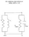
도 1은, 본 실시 형태에서의 제1 실시예에 상당하는 태그 안테나의 기본 구성의 설명도이다. 도 1에서, 표면 도체로서의 안테나 패치(Cu)(1)와, 이면 도체(Cu)(2) 사이에 유전체 스페이서(3)가 끼워진 형식으로 태그 안테나가 형성되어 있다. 유전체 스페이서(3)의 비유전율 εr의 값은 10 이상으로 하고, 여기에서는 예를 들면 12인 것으로 한다.1 is an explanatory diagram of a basic configuration of a tag antenna corresponding to the first embodiment of the present embodiment. In Fig. 1, a tag antenna is formed in such a manner that a
안테나 패치(1)측에 IC칩이 탑재된 태그 전체의 크기는, 예를 들면 54 mm×39 mm×4 mm인 것으로 한다. 이 치수는, 기본적으로는 유전체 스페이서(3)의 크기에 의해 결정되는 것으로 하고, 표면 도체로서의 안테나 패치(1)는 유전체 스페이서(3)보다도 작은 면적을 갖는 것으로 한다. 또한, 제1 실시예에서의 태그 안테나 의 안테나 패치(1)는 동장의 유전체 표면의 동판의 에칭에 의해 제조되는 것으로 한다.The size of the whole tag in which the IC chip is mounted on the
표면 도체로서의 안테나 패치(1) 위에서, 도시되어 있는 x 좌표의 "0" 부근을 중심으로 하여 슬릿(4)이 형성되고, 또한 슬릿(4)과 안테나 패치(1)의 x축에 평행한 변과의 사이에 절결부가 형성되고, 이 절결부는 칩 탑재부(5)로서 이용된다. 즉 IC칩은 그 2개의 접속 단자가, 각각 이 절결부의 끝의 금속 부분에 접속되는 형식으로 탑재되어, 전체로서 RFID 태그로서 동작하게 된다.On the
안테나 패치(1) 위에서, 예를 들면 슬릿(4)이 존재하는 측의 변과 반대측의 변의 측에 컷트부(6)가 형성된다. 도 1의 태그 안테나 전체는, 후술하는 바와 같이 저항과 인덕턴스의 병렬 회로로서 등가적으로 표현되며, 전술한 슬릿(4)은 주로 인덕턴스의 조정용으로, 또한 컷트부(6)는 등가적인 저항의 조정용으로 이용된다.On the
본 실시 형태에서는 전술한 바와 마찬가지로 태그의 동작 주파수를 953 MHz로 한다. 이 때, 공기 중의 파장 λ는 약 315 mm이며, λ/2의 값은 약 157 mm로 된다. 그러나, 안테나 패치(1)를 유전체 스페이서(3) 위에 형성, 또는 접착하는 형식으로 전파의 송수신이 행해지기 때문에, 실제의 파장은 그보다 짧아진다.In the present embodiment, as described above, the operating frequency of the tag is 953 MHz. At this time, the wavelength? In the air is about 315 mm, and the value of? / 2 is about 157 mm. However, since the radio wave is transmitted and received in a manner of forming or bonding the
일반적으로 비유전율 εr의 유전체의 내부에서의 전파의 파장은 공기 중에 비하여In general, the wavelength of radio waves in a dielectric having a relative dielectric constant?

로 되지만, 도 1과 같은 구조에서는, 안테나 패치(1)의 주변에는 유전체 스페이 서(3) 뿐만 아니라, 공기도 존재하기 때문에, 파장 λ는 중간적인 값으로 되고, λ/2 의 값은, 예를 들면 70∼80 mm 정도로 된다.In the structure as shown in FIG. 1, since not only the
본 실시 형태에서는, 태그 안테나의 사이즈, 예를 들면 도 1에서 슬릿(4)과 평행한 방향의 안테나 패치(1)의 길이를, 이 λ/2의 값보다 작게 하는 점에 특징이 있다. 이 방향의 유전체 스페이서(3)의 길이는 54 mm이며, 안테나 패치(1)의 이 방향의 길이는 제조상의 마진을 고려하여 당연히 54 mm보다 작고, 따라서 λ/2보다 짧은 길이로 된다. 그 의미에서 도 1에서의 안테나 패치(1)를 미소 패치라고 부르기로 하는데, 이 미소 패치를 이용하는 구조에서는, 안테나의 방사 효율은 λ/2 공진을 이용하는 경우보다도 약간 저하하지만, 소형화, 및 저코스트화라고 하는 관점에서는 바람직한 것으로 된다.This embodiment is characterized in that the size of the tag antenna, for example, the length of the
또한, 전술한 바와 같이, 특허 문헌 1에서는 스페이서의 두께가 30 mm 이상일 때에 판독 거리가 최대로 된다고 되어 있지만, 본 실시 형태에서는 유전체 스페이서의 두께가 두꺼우면 태그 안테나로서 적절한 동작이 행해지지 않아, 그 두께를 1∼10 mm의 범위 내로 할 필요가 있다.As described above, in
도 2는, 도 1의 태그 안테나와 IC칩의 임피던스의 설명도이다. 여기에서 도 1의 칩 탑재부(5)에 탑재되는 IC칩은, 등가적으로 Rc=1400 Ω의 저항과, Cc=0.7 pF의 정전 용량의 병렬 회로로 표현되는 것으로 한다. 이 칩과 태그 안테나의 정합을 도모하기 위해, 태그 안테나의 등가 회로를 안테나 방사 저항 Ra, 인덕턴스 La의 병렬 회로로 표현하였을 때에, 인덕턴스 La와 칩의 정전 용량 Cc사이에 공진 조건 이 성립함과 함께, 안테나 방사 저항 Ra와 칩의 저항 Rc의 값이 동일하게 되는 것이 필요하다. 전술한 공진 조건이 성립할 때, 동작 주파수 fo과 La, 및 Cc사이에는 하기 수학식 1이 성립한다.2 is an explanatory diagram of impedances of the tag antenna and the IC chip of FIG. 1. IC chip here is also mounted on the

도 1에서는, 태그 안테나의 등가적인 인덕턴스 La는, 칩 탑재부(5)로서의 절결부의 길이를 제외하고, 슬릿(4)을 일주하는 금속 부분의 길이에 의해 기본적으로 결정된다. 따라서, 이 슬릿의 폭보다도 그 길이가 인덕턴스 La를 기본적으로 결정하는 것으로 된다. 또한, 칩 탑재부(5)로서의 절결부의 주위 전체가 안테나 방사 저항 Ra를 결정하는 부분으로 되는데, 여기에 컷트부(6)를 형성하고, 이 컷트부(6)의 치수를 조정함으로써 안테나 방사 저항 Ra의 값을 칩의 입력 저항 Rc의 값과 거의 동일한 값으로 조정하는 것으로 한다. 또한, 예를 들면 안테나 패치(1)나 슬릿(4)의 치수에 따라서는, 컷트부(6)를 형성하지 않고 임피던스를 정합시키는 것도 가능하다.In FIG. 1, the equivalent inductance La of the tag antenna is basically determined by the length of the metal portion that circumscribes the
도 3은, 태그 안테나의 제1 실시예에서의 전류 분포의 설명도이다. 전류는, 도 1에서 설명한 슬릿(4)의 방향, 즉 좌우 방향으로 흐르고, 충분한 전파가 방사된다. 전술한 바와 같이 안테나 패치(1)의 좌우 방향의 길이가, 예를 들면 λ/2에 상당하는 70∼80 mm 정도이면 λ/2 공진으로서 큰 전류가 흐르지만, 본 실시 형태에서는 그 길이는 54 mm 이하이며, λ/2보다도 짧기 때문에 전류의 크기는 약간 작아지지만, 태그의 중앙 부근에서는 비교적 큰 전류가 흐른다. 또한, 안테나 패치(1)의 좌우의 끝의 변 위에서 전류의 크기는 "0"으로 된다.3 is an explanatory diagram of a current distribution in the first embodiment of the tag antenna. An electric current flows in the direction of the
도 3의 안테나 패치(1)의 도면에서, 슬릿(4)의 길이 S2의 조정과, 컷트부(6)의 깊이 방향의 길이 S1의 조정에 의해, 도 2에서 설명한 바와 같이 인덕턴스 La와 칩의 용량 Cc가 동작 주파수에서의 공진 조건을 만족하도록, 또한 안테나 방사 저항 Ra와 칩의 저항 Rc가 동등하게 되도록 조정을 행하는 것으로 한다. 전술한 바와 같이, 컷트부(6)의 깊이 S1에 의해 안테나 방사 저항 Ra의 값이 기본적으로 결정되고, 또한 슬릿(4)의 길이 S2의 값에 의해 인덕턴스 La의 값이 기본적으로 결정된다. 예를 들면 컷트부(6)의 좌우 방향의 폭은 여기에서는 일정하지만, 이 폭을 변화시키는 것에 의해서도, 안테나 방사 저항 Ra의 값을 조정하는 것이 가능하다.In the diagram of the
도 4 및 도 5는, 컷트부(6)의 깊이 S1, 및 슬릿(4)의 길이 S2의 조정에 의한 안테나 방사 저항 Ra와 인덕턴스 La의 계산 결과의 설명도이다. 도 4에서는, 컷트부(6)의 깊이 S1의 값을 파라미터로 하여, 슬릿의 길이 S2에 대한 안테나 방사 저항 Ra의 계산 결과가 도시되어 있는데, 컷트부(6)의 깊이 S1의 값을 7 mm로 함으로써, 슬릿(4)의 길이 S2의 값과는 그다지 관계없이, 안테나 방사 저항 Ra의 값을 칩의 저항 Rc의 값과 동등하게 하는 것이 가능한 것이 도시되어 있다.4 and 5 are explanatory diagrams of calculation results of the antenna radiation resistance Ra and the inductance La by adjusting the depth S1 of the
도 5에서는, 슬릿(4)의 길이 S2에 대한 인덕턴스 La의 계산 결과가, 컷트부(6)의 깊이 S1을 파라미터로 하여 도시되어 있는데, 도 4에서 설명한 바와 같이 S1의 값을 7 mm로 하면, 슬릿(4)의 길이 S2의 값을 12 mm로 함으로써, 칩의 용량 Cc=0.7 pF와 동작 주파수에서 공진 조건을 만족하는 임피던스 La의 값으로서의 40 nH가 얻어지는 것을 알 수 있다. 또한, 도 4, 도 5는 계산 결과이지만, 실제로는 여기에서 얻어진 값, 즉 S1=7 mm와, S2=12 mm의 부근에서, 실제의 컷트부(6)의 깊이, 및 슬릿(4)의 길이를 미세 조정함으로써, 태그 안테나로서 실용적으로 충분한 특성이 얻어진다.In Figure 5, the values of S1, as the length of the
도 6은, 이와 같이 하여 결정된 S1과 S2의 치수에 대응하는, 안테나와 칩의 반사 계수 S11을 나타낸다. 동작 주파수 953 MHz에서의 반사 계수의 값은 -11.7 dB 정도이며, 충분한 정합 상태가 얻어지고 있는 것을 알 수 있다.6 shows the reflection coefficient S11 of the antenna and the chip, corresponding to the dimensions of S1 and S2 determined in this way. The value of the reflection coefficient at the operating frequency of 953 MHz is about -11.7 dB, and it can be seen that a sufficient matching state is obtained.
도 7은, 제1 실시예에서의 태그 안테나의 안테나 게인의 주파수 특성을 도시한다. 동작 주파수의 953 MHz에서 1 dBi 정도의 게인이 얻어지고 있다. 또한, 여기에서 dBi는 전파를 점으로부터 방사할 때에, 예를 들면 전계 분포가 깨끗한 구의 상태로 될 때를 0 dB로 한 게인의 단위이다.Fig. 7 shows the frequency characteristics of the antenna gain of the tag antenna in the first embodiment. A gain of about 1 dBi is obtained at 953 MHz of operating frequency. In addition, dBi here is a unit of the gain which made 0 dB when radiating a radio wave from a point, for example, when the electric field distribution becomes a state of a clean sphere.
도 8은, 도 6과 도 7을 기초하여 통신 거리를 계산한 결과이다. 이 계산 결 과는, 칩의 동작 전력을 -9 dBm, 리더/라이터의 출력을 1 W, 리더/라이터측의 안테나 게인을 6 dBi로 한 것이며, 953 MHz에서 통신 거리로서 약 3 m의 값이 얻어지고 있다. 또한, 여기에서 dBm은 파워 ×103을 데시벨 표시한 값이다.8 is a result of calculating the communication distance based on FIGS. 6 and 7. This calculation resulted in a chip operating power of -9 dBm, a reader / writer output of 1 W, and an antenna gain on the reader / writer side of 6 dBi. It is obtained. In this case, dBm is a value expressed in decibels of
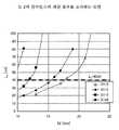
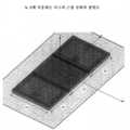
도 9 및 도 10은, 제1 실시예의 태그 안테나를 복수개 배열한 경우의 통신 거리의 설명도이다. 도 9의 계산 결과는, 도 10과 같이 태그 안테나를 배치한 경우의 통신 거리의 계산 결과이다.9 and 10 are explanatory diagrams of communication distances when a plurality of tag antennas of the first embodiment are arranged. The calculation result of FIG. 9 is a calculation result of the communication distance when a tag antenna is arrange | positioned like FIG.
일반적으로 하나의 물체에 태그를 1개 접착한다고 하여도, 물체의 배치 상태에 따라서는 태그가 꽤 접근하게 될 가능성이 있다. 도 10은, 그러한 상태를 극단적으로 도시한 것이다. 안테나 패치의 길이가 λ/2에 일치하는 경우에 태그를 근접하여 배열하면, 인접하는 태그 사이에서 전파의 간섭이 일어나, 통신 거리가 격감한다고 하는 문제점이 있다. RFID 시스템에서는, 태그가 접근한 상태에서 이용될 가능성도 많으며, 그러한 경우에도 통신 거리가 떨어지지 않는 것이 실용적으로 매우 중요하다.In general, even if one tag is attached to an object, the tag may be quite accessible depending on the arrangement of the objects. Fig. 10 shows such a state extremely. If the tags are arranged in close proximity when the length of the antenna patch is equal to λ / 2, interference of radio waves occurs between adjacent tags, resulting in a decrease in communication distance. In an RFID system, there is a high possibility that the tag is used in the approached state, and even in such a case, it is practically important that the communication distance does not drop.
도 9에서는, 태그를 1개만 사용한 경우, 즉 n=1의 상태와, n이 2 또는 3인 상태에서, 동작 주파수 953 MHz에서의 통신 거리는 3 m 이상이며, 도 10과 같은 극단적인 배치 상태에서도 태그의 통신 거리가 떨어지지 않는 것이 도시되어 있다. 이것은 제1 실시예에서, 안테나 패치(1)의 사이즈, 즉 좌우 방향의 길이가 λ/2보다 짧은 것에 의한 효과이다.In FIG. 9, when only one tag is used, that is, in a state where n = 1 and n is 2 or 3, the communication distance at an operating frequency of 953 MHz is 3 m or more, even in an extreme arrangement as shown in FIG. It is shown that the communication distance of the tag does not drop. This is the effect of the size of the
이하, 도 11 내지 도 13을 이용하여 제2, 제3 실시예에 대하여 설명한다. 이들 제2, 제3 실시예에서, 안테나 패치를 포함하는 태그 안테나의 기본적 구성은 제1 실시예에서와 마찬가지이지만, 제조상의 공정이 제1 실시예와 다르다.Hereinafter, the second and third embodiments will be described with reference to FIGS. 11 to 13. In these second and third embodiments, the basic configuration of the tag antenna including the antenna patch is the same as in the first embodiment, but the manufacturing process is different from that in the first embodiment.
도 11은, 제2 실시예에서의 태그 안테나의 제조 공정의 설명도이다. 제1 실시예에서는, 특히 도 1의 안테나 패치(1)의 제조 공정에서, 미리 유전체 스페이서(3) 위에 동판이 깔린 동장판의 금속 부분을 에칭하여 만드는 것으로 하였지만, 도 11의 제2 실시예에서는, 안테나 패턴 시트는 미리, 예를 들면 롤 형상의 금속 시트로서 만들어 두고, 그 안테나 패턴 시트(10)를 유전체 스페이서로서의 세라믹 수지(12)의 상면에, 또한 반사판(11)을 하면에 접착함으로써 태그 안테나의 제조가 행해진다. 이에 의해 동장판을 에칭하는 제1 실시예에 비교하여 코스트를 낮추는 것이 가능하게 된다.11 is an explanatory diagram of a manufacturing process of a tag antenna according to the second embodiment. In the first embodiment, particularly in the manufacturing process of the
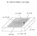
도 12는, 제3 실시예의 제조 공정의 설명도이다. 도 12를 도 11의 제2 실시예와 비교하면, 안테나 패턴 시트(10)의 상하에 우레탄 수지(13, 14)가 더 접착되는 점이 서로 다르다. 이 우레탄 수지(13, 14)는 IC칩을 포함하는 안테나 패치의 대환경성을 향상시키기 위한 것이며, 부식 환경이나 고온 상태에서도 확실하게 동작하는 태그를 제공하는 것이 가능하게 된다.12 is an explanatory diagram of a manufacturing process of the third embodiment. When FIG. 12 is compared with the second embodiment of FIG. 11, the urethane resins 13 and 14 are further bonded to the top and bottom of the
도 13은, 도 12에서 설명한 제3 실시예로서의 태그의 제품 상태를 도시한다. 도 13에서 안테나 패턴 시트(10), 즉 안테나 패치는 우레탄 수지(13, 14)와의 사이에 끼워지며, 세라믹 수지(12)의 상면에 접착되고, 또한 반사판(11)이 세라믹 수지(12)의 하면에 접착된 상태가 도시되어 있다.FIG. 13 shows the product state of the tag as the third embodiment explained in FIG. In FIG. 13, the
이상에서 본 실시 형태에서의 태그 안테나 및 태그의 특성에 대하여 상세하 게 설명하였지만, 태그를 금속에 접착하는 경우에는, 유전체 스페이서의 이면(하면)의 도체, 즉 반사판은 불필요로 된다.Although the characteristics of the tag antenna and the tag in the present embodiment have been described in detail above, in the case where the tag is adhered to a metal, a conductor, i.e., a reflector, on the back surface (lower surface) of the dielectric spacer becomes unnecessary.
또한, 도 1에서 설명한 칩 탑재부는 좌표 x=0 부근, 즉 안테나 패치의 중앙 부근에 배치하는 것으로 하였지만, 예를 들면 태그의 상면에 바 코드나 문자의 인자 등을 하는 경우에는 칩이 솟아 오른 것이 방해로 되는 경우가 있기 때문에, 칩 탑재부, 및 인덕턴스 형성을 위한 슬릿을 안테나 패치의 끝 쪽으로 치우치게 하는 것도 가능하다.In addition, although the chip mounting part described with reference to FIG. 1 is arrange | positioned near coordinate x = 0, ie near the center of an antenna patch, for example, when chip | tip printing of a bar code, a character, etc. on the upper surface of a tag, the chip rose. It is also possible to bias the chip mounting portion and the slit for inductance formation toward the end of the antenna patch because it may be a hindrance.
이상 상세하게 설명한 바와 같이, 본 실시 형태에 의하면, 사이즈가 54 mm×39 mm×4 mm와 같이 매우 소형이면서, 금속에 접착하여도 약 3 m의 통신 거리가 얻어지는 태그를 제공 가능하게 된다. 이 태그에서는 상하 접속의 쓰루홀이 불필요하며, 또한 임피던스 정합을 위한 조정 개소는 슬릿의 길이와 컷트부의 깊이의 2개소만이며, 조정의 공수가 적어, 코스트를 저하시킬 수 있다. 또한, 복수의 태그를 근접하여 배열하여도, 태그 1개의 경우와 동등한 통신 거리를 얻을 수 있어, 실용적이고 성능이 좋은 RFID 시스템의 구축에 기여하는 바가 크다.As described in detail above, according to the present embodiment, it is possible to provide a tag which is very small in size, such as 54 mm x 39 mm x 4 mm, and which has a communication distance of about 3 m even when attached to a metal. In this tag, through-holes for vertical connection are unnecessary, and only two places for adjusting the impedance are the length of the slit and the depth of the cut part, and the man-hour of adjustment is small, which can reduce the cost. Further, even when a plurality of tags are arranged in close proximity, a communication distance equivalent to that of one tag can be obtained, which contributes to the construction of a practical and high-performance RFID system.
도 1은, 제1 실시예에 상당하는 태그 안테나의 기본 구성을 도시하는 도면.1 is a diagram showing a basic configuration of a tag antenna corresponding to the first embodiment.
도 2는, 태그 안테나와 IC칩의 임피던스의 정합을 설명하는 도면.2 is a diagram for explaining matching of impedance between a tag antenna and an IC chip.
도 3은, 안테나 패치 상의 전류 분포를 설명하는 도면.3 is a diagram illustrating a current distribution on an antenna patch.
도 4는, 도 2의 안테나 방사 저항의 계산 결과를 도시하는 도면.FIG. 4 is a diagram showing a calculation result of the antenna radiation resistance of FIG. 2. FIG.
도 5는, 도 2의 인덕턴스의 계산 결과를 도시하는 도면.FIG. 5 is a diagram showing a result of calculating the inductance of FIG. 2. FIG.
도 6은, 태그 안테나와 IC칩의 반사 계수의 계산 결과를 도시하는 도면.Fig. 6 is a diagram showing the calculation result of reflection coefficients of a tag antenna and an IC chip.
도 7은, 태그 안테나의 게인의 계산 결과를 도시하는 도면.7 is a diagram showing a calculation result of a gain of a tag antenna.
도 8은, 태그 안테나의 통신 거리의 계산 결과를 도시하는 도면.8 is a diagram illustrating a calculation result of a communication distance of a tag antenna.
도 9는, 태그의 근접 상태에서의 통신 거리의 계산 결과를 도시하는 도면.9 is a diagram illustrating a calculation result of a communication distance in a proximity state of a tag.
도 10은, 도 9에 대응하는 태그의 근접 상태의 설명도.10 is an explanatory diagram of a proximity state of a tag corresponding to FIG. 9;
도 11은, 제2 실시예의 태그 안테나의 제조 공정의 설명도.11 is an explanatory diagram of a manufacturing process of a tag antenna according to the second embodiment.
도 12는, 제3 실시예의 태그 안테나의 제조 공정의 설명도.12 is an explanatory diagram of a manufacturing process of a tag antenna according to the third embodiment;
도 13은, 제3 실시예의 태그 안테나의 제품 형상을 도시하는 도면.Fig. 13 is a diagram showing the product shape of the tag antenna of the third embodiment.
도 14는, 태그 안테나의 종래예의 구성의 설명도.14 is an explanatory diagram of a configuration of a conventional example of a tag antenna.
도 15는, 태그 안테나의 종래예의 근접 상태에서의 통신 거리의 설명도.15 is an explanatory diagram of a communication distance in a proximity state of a conventional example of a tag antenna.
<도면의 주요 부분에 대한 부호의 설명><Explanation of symbols for the main parts of the drawings>
1: 안테나 패치1: antenna patch
2: 이면 도체2: backside conductor
3: 유전체 스페이서3: dielectric spacer
4: 슬릿4: slit
5: 칩 탑재부5: chip mounting part
6: 컷트부6: cut
10: 안테나 패턴 시트10: antenna pattern sheet
11: 반사판11: reflector
12: 세라믹 수지12: ceramic resin
13, 14: 우레탄 수지13, 14: urethane resin
Claims (10)
Translated fromKoreanApplications Claiming Priority (2)
| Application Number | Priority Date | Filing Date | Title |
|---|---|---|---|
| JPJP-P-2007-00223813 | 2007-08-30 | ||
| JP2007223813AJP5086004B2 (en) | 2007-08-30 | 2007-08-30 | Tag antenna and tag |
Publications (2)
| Publication Number | Publication Date |
|---|---|
| KR20090023052Atrue KR20090023052A (en) | 2009-03-04 |
| KR100970072B1 KR100970072B1 (en) | 2010-07-16 |
Family
ID=39877890
Family Applications (1)
| Application Number | Title | Priority Date | Filing Date |
|---|---|---|---|
| KR1020080056458AExpired - Fee RelatedKR100970072B1 (en) | 2007-08-30 | 2008-06-16 | Tag antenna, and tag |
Country Status (6)
| Country | Link |
|---|---|
| US (1) | US7859414B2 (en) |
| EP (1) | EP2031698A1 (en) |
| JP (1) | JP5086004B2 (en) |
| KR (1) | KR100970072B1 (en) |
| CN (1) | CN101378145B (en) |
| TW (1) | TWI362783B (en) |
Cited By (1)
| Publication number | Priority date | Publication date | Assignee | Title |
|---|---|---|---|---|
| KR101309238B1 (en)* | 2012-08-14 | 2013-09-17 | 동국대학교 산학협력단 | Spidron fractal antenna for multiband |
Families Citing this family (20)
| Publication number | Priority date | Publication date | Assignee | Title |
|---|---|---|---|---|
| US8800876B2 (en)* | 2008-08-11 | 2014-08-12 | Martin S. Casden | Ruggedized RFID tag and reader |
| JP5230302B2 (en)* | 2008-08-26 | 2013-07-10 | ニッタ株式会社 | Wireless IC tag and wireless communication system |
| JP4618459B2 (en)* | 2008-09-05 | 2011-01-26 | オムロン株式会社 | RFID tag, RFID tag set and RFID system |
| JP5114357B2 (en)* | 2008-10-09 | 2013-01-09 | 株式会社日立製作所 | Wireless IC tag |
| KR101070486B1 (en)* | 2010-01-08 | 2011-10-05 | 엘에스산전 주식회사 | Radio Frequency Identification Tag |
| JP5358489B2 (en)* | 2010-03-11 | 2013-12-04 | 株式会社日立製作所 | RFID tag and manufacturing method thereof |
| JP4815643B1 (en)* | 2010-04-16 | 2011-11-16 | 幸裕 福島 | UHF band IC tag for urine sensor and HF band IC tag for urine sensor |
| JP5644397B2 (en)* | 2010-11-11 | 2014-12-24 | 富士通株式会社 | Wireless device and antenna device |
| US8730045B2 (en)* | 2010-12-16 | 2014-05-20 | Avery Dennison Corporation | Isolating and RFID-based sensor from environmental interference |
| CN102820531B (en) | 2011-06-08 | 2016-09-28 | 刘智佳 | There is the RFID label antenna of collocation structure, RFID label tag and system |
| KR101323690B1 (en)* | 2011-06-10 | 2013-10-30 | (주) 네톰 | Edge type dipole antenna and pcb provided with the same |
| WO2013068043A1 (en)* | 2011-11-10 | 2013-05-16 | Amb I.T. Holding B.V. | Tag assembly |
| CN104346647A (en)* | 2014-08-27 | 2015-02-11 | 北京中电华大电子设计有限责任公司 | Plane broadband passive electronic tag |
| US10109920B2 (en) | 2015-09-09 | 2018-10-23 | The Johns Hopkins University | Metasurface antenna |
| JP2016149146A (en)* | 2016-03-23 | 2016-08-18 | エーエムビー アイ.ティー.ホールディング ビーブイ | Tag assembly, tag structure, and bib for sport |
| CN108306096A (en)* | 2017-01-12 | 2018-07-20 | 南宁富桂精密工业有限公司 | A kind of anti-metal tag antenna and the electronic labelling system comprising the antenna |
| TWI631510B (en)* | 2017-06-06 | 2018-08-01 | 創新聯合科技股份有限公司 | Long distance wireless identification livestock ear tag female buckle structure |
| CN109713426A (en)* | 2018-11-19 | 2019-05-03 | 北京计算机技术及应用研究所 | A kind of RFID label antenna suitable for vehicle glass surface |
| US11380976B2 (en)* | 2019-01-03 | 2022-07-05 | Pallas LLC | Overboard tracking patch |
| CN111541017B (en)* | 2020-04-15 | 2022-07-15 | 烽火通信科技股份有限公司 | High-gain microstrip antenna and manufacturing method thereof |
Family Cites Families (18)
| Publication number | Priority date | Publication date | Assignee | Title |
|---|---|---|---|---|
| JP3029179B2 (en)* | 1993-04-28 | 2000-04-04 | キヤノン株式会社 | Liquid crystal element |
| US6018299A (en)* | 1998-06-09 | 2000-01-25 | Motorola, Inc. | Radio frequency identification tag having a printed antenna and method |
| US6107920A (en)* | 1998-06-09 | 2000-08-22 | Motorola, Inc. | Radio frequency identification tag having an article integrated antenna |
| JP2002298106A (en) | 2001-03-30 | 2002-10-11 | Seiko Precision Inc | Contactless ic tag |
| JP4348282B2 (en)* | 2004-06-11 | 2009-10-21 | 株式会社日立製作所 | Wireless IC tag and method of manufacturing wireless IC tag |
| DE102004034768B4 (en)* | 2004-07-19 | 2007-11-15 | Infineon Technologies Ag | Identification media |
| DE602005021513D1 (en) | 2004-08-26 | 2010-07-08 | Nxp Bv | RFID LABEL WITH FOLDED DIPOL |
| DE102004045707A1 (en) | 2004-09-21 | 2006-03-30 | Fraunhofer-Gesellschaft zur Förderung der angewandten Forschung e.V. | antenna |
| JP2006140735A (en) | 2004-11-11 | 2006-06-01 | Toshiba Corp | Planar antenna |
| KR20100021665A (en)* | 2004-12-14 | 2010-02-25 | 후지쯔 가부시끼가이샤 | Antenna and noncontact tag |
| JP4281683B2 (en)* | 2004-12-16 | 2009-06-17 | 株式会社デンソー | IC tag mounting structure |
| JP2006237674A (en) | 2005-02-22 | 2006-09-07 | Suncall Corp | Patch antenna and rfid inlet |
| JP2006311372A (en)* | 2005-04-28 | 2006-11-09 | Hitachi Ltd | Wireless IC tag |
| JP4500214B2 (en)* | 2005-05-30 | 2010-07-14 | 株式会社日立製作所 | Wireless IC tag and method of manufacturing wireless IC tag |
| JP5043656B2 (en) | 2005-06-16 | 2012-10-10 | 富士通株式会社 | Tag antenna and tag |
| KR100690849B1 (en) | 2005-11-04 | 2007-03-09 | 연세대학교 산학협력단 | HF band printing antenna |
| JP2007201743A (en)* | 2006-01-26 | 2007-08-09 | Renesas Technology Corp | Id tag |
| JP4437475B2 (en)* | 2006-01-31 | 2010-03-24 | 富士通株式会社 | Folded dipole antenna and tag using the same |
- 2007
- 2007-08-30JPJP2007223813Apatent/JP5086004B2/ennot_activeExpired - Fee Related
- 2008
- 2008-05-21TWTW097118662Apatent/TWI362783B/ennot_activeIP Right Cessation
- 2008-05-23EPEP08156841Apatent/EP2031698A1/ennot_activeCeased
- 2008-05-28USUS12/128,439patent/US7859414B2/ennot_activeExpired - Fee Related
- 2008-06-16CNCN200810109989.4Apatent/CN101378145B/ennot_activeExpired - Fee Related
- 2008-06-16KRKR1020080056458Apatent/KR100970072B1/ennot_activeExpired - Fee Related
Cited By (1)
| Publication number | Priority date | Publication date | Assignee | Title |
|---|---|---|---|---|
| KR101309238B1 (en)* | 2012-08-14 | 2013-09-17 | 동국대학교 산학협력단 | Spidron fractal antenna for multiband |
Also Published As
| Publication number | Publication date |
|---|---|
| JP5086004B2 (en) | 2012-11-28 |
| US7859414B2 (en) | 2010-12-28 |
| CN101378145A (en) | 2009-03-04 |
| TW200910687A (en) | 2009-03-01 |
| TWI362783B (en) | 2012-04-21 |
| EP2031698A1 (en) | 2009-03-04 |
| CN101378145B (en) | 2012-12-26 |
| KR100970072B1 (en) | 2010-07-16 |
| US20090058658A1 (en) | 2009-03-05 |
| JP2009060217A (en) | 2009-03-19 |
Similar Documents
| Publication | Publication Date | Title |
|---|---|---|
| KR100970072B1 (en) | Tag antenna, and tag | |
| JP4498364B2 (en) | Antenna and contactless tag | |
| JP4393228B2 (en) | Small antenna and wireless tag provided with the same | |
| JP4359198B2 (en) | IC tag mounting substrate manufacturing method | |
| JP4281683B2 (en) | IC tag mounting structure | |
| KR100817395B1 (en) | Folded dipole antenna and tag using the same | |
| US8678295B2 (en) | Miniaturized radio-frequency identification tag and microstrip patch antenna thereof | |
| CN100566021C (en) | Antenna assembly | |
| KR100848237B1 (en) | Wireless tag and antenna for wireless tag | |
| EP1653396B1 (en) | RFID tag | |
| EP1716711B1 (en) | Slotted multiple band antenna | |
| US20080122628A1 (en) | RFID tag antenna and RFID tag | |
| JP2007324709A (en) | Cross dipole antenna, tag using this | |
| CN109219906A (en) | Antenna assembly | |
| CN1256805A (en) | Communication Antennas and Devices | |
| WO2007029296A1 (en) | Rf tag and method for manufacturing rf tag | |
| KR100778120B1 (en) | Antenna with extended operating frequency bandwidth | |
| JP2007081632A (en) | Radio ic tag | |
| US7375697B2 (en) | Meandered slit antenna | |
| KR100993274B1 (en) | Flat antenna with beam direction control and applicable to radio recognition tags | |
| JP2007221735A (en) | S-shaped plate-like small-sized dipole antenna for electronic tag, and electronic tag provided with the same | |
| KR20150029773A (en) | HF UHF multi-band RFID tag antenna | |
| JP4438844B2 (en) | RFID tag | |
| JP4235513B2 (en) | Multi-band multi-element patch antenna | |
| JP2009065251A (en) | RFID tag |
Legal Events
| Date | Code | Title | Description |
|---|---|---|---|
| A201 | Request for examination | ||
| PA0109 | Patent application | St.27 status event code:A-0-1-A10-A12-nap-PA0109 | |
| PA0201 | Request for examination | St.27 status event code:A-1-2-D10-D11-exm-PA0201 | |
| PG1501 | Laying open of application | St.27 status event code:A-1-1-Q10-Q12-nap-PG1501 | |
| D13-X000 | Search requested | St.27 status event code:A-1-2-D10-D13-srh-X000 | |
| D14-X000 | Search report completed | St.27 status event code:A-1-2-D10-D14-srh-X000 | |
| E902 | Notification of reason for refusal | ||
| PE0902 | Notice of grounds for rejection | St.27 status event code:A-1-2-D10-D21-exm-PE0902 | |
| E13-X000 | Pre-grant limitation requested | St.27 status event code:A-2-3-E10-E13-lim-X000 | |
| P11-X000 | Amendment of application requested | St.27 status event code:A-2-2-P10-P11-nap-X000 | |
| P13-X000 | Application amended | St.27 status event code:A-2-2-P10-P13-nap-X000 | |
| E701 | Decision to grant or registration of patent right | ||
| PE0701 | Decision of registration | St.27 status event code:A-1-2-D10-D22-exm-PE0701 | |
| GRNT | Written decision to grant | ||
| PR0701 | Registration of establishment | St.27 status event code:A-2-4-F10-F11-exm-PR0701 | |
| PR1002 | Payment of registration fee | St.27 status event code:A-2-2-U10-U11-oth-PR1002 Fee payment year number:1 | |
| PG1601 | Publication of registration | St.27 status event code:A-4-4-Q10-Q13-nap-PG1601 | |
| FPAY | Annual fee payment | Payment date:20130621 Year of fee payment:4 | |
| PR1001 | Payment of annual fee | St.27 status event code:A-4-4-U10-U11-oth-PR1001 Fee payment year number:4 | |
| FPAY | Annual fee payment | Payment date:20140626 Year of fee payment:5 | |
| PR1001 | Payment of annual fee | St.27 status event code:A-4-4-U10-U11-oth-PR1001 Fee payment year number:5 | |
| FPAY | Annual fee payment | Payment date:20150618 Year of fee payment:6 | |
| PR1001 | Payment of annual fee | St.27 status event code:A-4-4-U10-U11-oth-PR1001 Fee payment year number:6 | |
| FPAY | Annual fee payment | Payment date:20160616 Year of fee payment:7 | |
| PR1001 | Payment of annual fee | St.27 status event code:A-4-4-U10-U11-oth-PR1001 Fee payment year number:7 | |
| P22-X000 | Classification modified | St.27 status event code:A-4-4-P10-P22-nap-X000 | |
| FPAY | Annual fee payment | Payment date:20170616 Year of fee payment:8 | |
| PR1001 | Payment of annual fee | St.27 status event code:A-4-4-U10-U11-oth-PR1001 Fee payment year number:8 | |
| PR1001 | Payment of annual fee | St.27 status event code:A-4-4-U10-U11-oth-PR1001 Fee payment year number:9 | |
| FPAY | Annual fee payment | Payment date:20190617 Year of fee payment:10 | |
| PR1001 | Payment of annual fee | St.27 status event code:A-4-4-U10-U11-oth-PR1001 Fee payment year number:10 | |
| PC1903 | Unpaid annual fee | St.27 status event code:A-4-4-U10-U13-oth-PC1903 Not in force date:20200707 Payment event data comment text:Termination Category : DEFAULT_OF_REGISTRATION_FEE | |
| PC1903 | Unpaid annual fee | St.27 status event code:N-4-6-H10-H13-oth-PC1903 Ip right cessation event data comment text:Termination Category : DEFAULT_OF_REGISTRATION_FEE Not in force date:20200707 |